 | –≠–ª–µ–∫—Ç—Ä–æ–Ω–Ω—ã–π –∫–æ–º–ø–æ–Ω–µ–Ω—Ç: HD6432675 | –°–∫–∞—á–∞—Ç—å:  PDF PDF  ZIP ZIP |

Regarding the change of names mentioned in the document, such as Hitachi
Electric and Hitachi XX, to Renesas Technology Corp.
The semiconductor operations of Mitsubishi Electric and Hitachi were transferred to Renesas
Technology Corporation on April 1st 2003. These operations include microcomputer, logic, analog
and discrete devices, and memory chips other than DRAMs (flash memory, SRAMs etc.)
Accordingly, although Hitachi, Hitachi, Ltd., Hitachi Semiconductors, and other Hitachi brand
names are mentioned in the document, these names have in fact all been changed to Renesas
Technology Corp. Thank you for your understanding. Except for our corporate trademark, logo and
corporate statement, no changes whatsoever have been made to the contents of the document, and
these changes do not constitute any alteration to the contents of the document itself.
Renesas Technology Home Page: http://www.renesas.com
Renesas Technology Corp.
Customer Support Dept.
April 1, 2003
To all our customers

Cautions
Keep safety first in your circuit designs!
1. Renesas Technology Corporation puts the maximum effort into making semiconductor products better
and more reliable, but there is always the possibility that trouble may occur with them. Trouble with
semiconductors may lead to personal injury, fire or property damage.
Remember to give due consideration to safety when making your circuit designs, with appropriate
measures such as (i) placement of substitutive, auxiliary circuits, (ii) use of nonflammable material or
(iii) prevention against any malfunction or mishap.
Notes regarding these materials
1. These materials are intended as a reference to assist our customers in the selection of the Renesas
Technology Corporation product best suited to the customer's application; they do not convey any
license under any intellectual property rights, or any other rights, belonging to Renesas Technology
Corporation or a third party.
2. Renesas Technology Corporation assumes no responsibility for any damage, or infringement of any
third-party's rights, originating in the use of any product data, diagrams, charts, programs, algorithms, or
circuit application examples contained in these materials.
3. All information contained in these materials, including product data, diagrams, charts, programs and
algorithms represents information on products at the time of publication of these materials, and are
subject to change by Renesas Technology Corporation without notice due to product improvements or
other reasons. It is therefore recommended that customers contact Renesas Technology Corporation
or an authorized Renesas Technology Corporation product distributor for the latest product information
before purchasing a product listed herein.
The information described here may contain technical inaccuracies or typographical errors.
Renesas Technology Corporation assumes no responsibility for any damage, liability, or other loss
rising from these inaccuracies or errors.
Please also pay attention to information published by Renesas Technology Corporation by various
means, including the Renesas Technology Corporation Semiconductor home page
(http://www.renesas.com).
4. When using any or all of the information contained in these materials, including product data, diagrams,
charts, programs, and algorithms, please be sure to evaluate all information as a total system before
making a final decision on the applicability of the information and products. Renesas Technology
Corporation assumes no responsibility for any damage, liability or other loss resulting from the
information contained herein.
5. Renesas Technology Corporation semiconductors are not designed or manufactured for use in a device
or system that is used under circumstances in which human life is potentially at stake. Please contact
Renesas Technology Corporation or an authorized Renesas Technology Corporation product distributor
when considering the use of a product contained herein for any specific purposes, such as apparatus or
systems for transportation, vehicular, medical, aerospace, nuclear, or undersea repeater use.
6. The prior written approval of Renesas Technology Corporation is necessary to reprint or reproduce in
whole or in part these materials.
7. If these products or technologies are subject to the Japanese export control restrictions, they must be
exported under a license from the Japanese government and cannot be imported into a country other
than the approved destination.
Any diversion or reexport contrary to the export control laws and regulations of Japan and/or the
country of destination is prohibited.
8. Please contact Renesas Technology Corporation for further details on these materials or the products
contained therein.

Hitachi 16-Bit Single-Chip Microcomputer
H8S/2678Series, H8S/2678R Series
H8S/2676 F-ZTAT
TM
HD64F2676
H8S/2676
HD6432676
H8S/2675
HD6432675
H8S/2674R
HD6412674R
H8S/2673
HD6432673
H8S/2670
HD6412670
Hardware Manual
ADE-602-242A
Rev. 2.0
04/05/02
Hitachi, Ltd.

Rev. 2.0, 04/02, page ii of xliv
Cautions
1. Hitachi neither warrants nor grants licenses of any rights of Hitachi's or any third party's
patent, copyright, trademark, or other intellectual property rights for information contained in
this document. Hitachi bears no responsibility for problems that may arise with third party's
rights, including intellectual property rights, in connection with use of the information
contained in this document.
2. Products and product specifications may be subject to change without notice. Confirm that you
have received the latest product standards or specifications before final design, purchase or
use.
3. Hitachi makes every attempt to ensure that its products are of high quality and reliability.
However, contact Hitachi's sales office before using the product in an application that
demands especially high quality and reliability or where its failure or malfunction may directly
threaten human life or cause risk of bodily injury, such as aerospace, aeronautics, nuclear
power, combustion control, transportation, traffic, safety equipment or medical equipment for
life support.
4. Design your application so that the product is used within the ranges guaranteed by Hitachi
particularly for maximum rating, operating supply voltage range, heat radiation characteristics,
installation conditions and other characteristics. Hitachi bears no responsibility for failure or
damage when used beyond the guaranteed ranges. Even within the guaranteed ranges,
consider normally foreseeable failure rates or failure modes in semiconductor devices and
employ systemic measures such as fail-safes, so that the equipment incorporating Hitachi
product does not cause bodily injury, fire or other consequential damage due to operation of
the Hitachi product.
5. This product is not designed to be radiation resistant.
6. No one is permitted to reproduce or duplicate, in any form, the whole or part of this document
without written approval from Hitachi.
7.
Contact Hitachi's sales office for any questions regarding this document or Hitachi
semiconductor products.

Rev. 2.0, 04/02, page iii of xliv
General Precautions on Handling of Product
1. Treatment of NC Pins
Note:
Do not connect anything to the NC pins.
The NC (not connected) pins are either not connected to any of the internal circuitry or are
used as test pins or to reduce noise. If something is connected to the NC pins, the
operation of the LSI is not guaranteed.
2. Treatment of Unused Input Pins
Note:
Fix all unused input pins to high or low level.
Generally, the input pins of CMOS products are high-impedance input pins. If unused pins
are in their open states, intermediate levels are induced by noise in the vicinity, a pass-
through current flows internally, and a malfunction may occur.
3. Processing before Initialization
Note:
When power is first supplied, the product's state is undefined.
The states of internal circuits are undefined until full power is supplied throughout the
chip and a low level is input on the reset pin. During the period where the states are
undefined, the register settings and the output state of each pin are also undefined. Design
your system so that it does not malfunction because of processing while it is in this
undefined state. For those products which have a reset function, reset the LSI immediately
after the power supply has been turned on.
4. Prohibition of Access to Undefined or Reserved Addresses
Note:
Access to undefined or reserved addresses is prohibited.
The undefined or reserved addresses may be used to expand functions, or test registers
may have been be allocated to these addresses. Do not access these registers; the system's
operation is not guaranteed if they are accessed.

Rev. 2.0, 04/02, page iv of xliv
Configuration of This Manual
This manual comprises the following items:
1. General Precautions on Handling of Product
2. Configuration of This Manual
3. Preface
4. Contents
5. Overview
6. Description of Functional Modules
∑
CPU and System-Control Modules
∑
On-Chip Peripheral Modules
The configuration of the functional description of each module differs according to the
module. However, the generic style includes the following items:
i) Feature
ii) Input/Output Pin
iii) Register Description
iv) Operation
v) Usage Note
When designing an application system that includes this LSI, take notes into account. Each section
includes notes in relation to the descriptions given, and usage notes are given, as required, as the
final part of each section.
7. List of Registers
8. Electrical Characteristics
9. Appendix
10. Main Revisions and Additions in this Edition (only for revised versions)
The list of revisions is a summary of points that have been revised or added to earlier versions.
This does not include all of the revised contents. For details, see the actual locations in this
manual.
11. Index

Rev. 2.0, 04/02, page v of xliv
Preface
The H8S/2678 Series and H8S/2678R Series are microcomputers (MCU) made up of the
H8S/2600 CPU employing Hitachi's original architecture as their cores, and the peripheral
functions required to configure a system.
The H8S/2600 CPU has an internal 32-bit configuration, sixteen 16-bit general registers, and a
simple and optimized instruction set for high-speed operation. The H8S/2600 CPU can handle a
16-Mbyte linear address space.
This LSI is equipped with direct memory access controller (DMAC and EXDMAC) and data
transfer controller (DTC) bus masters, ROM and RAM memory, a 16-bit timer pulse unit (TPU), a
programmable pulse generator (PPG), an 8-bit timer (TMR), a watchdog timer (WDT), a serial
communication interface (SCI and IrDA), a 10-bit A/D converter, an 8-bit D/A converter, and I/O
ports as on-chip peripheral modules required for system configuration
A high functionality bus controller is also provided, enabling fast and easy connection of DRAM,
SDRAM, and other kinds of memory.
A single-power flash memory (F-ZTAT
TM
*) version and masked ROM version are available for
this LSI's ROM. The F-ZTAT version provides flexibility as it can be reprogrammed in no time to
cope with all situations from the early stages of mass production to full-scale mass production.
This is particularly applicable to application devices with specifications that will most probably
change.
This manual describes this LSI's hardware.
Note: * F-ZTAT
TM
is a trademark of Hitachi, Ltd.
Target Users:
This manual was written for users who will be using this LSI in the design of
application systems. Target users are expected to understand the fundamentals of
electrical circuits, logical circuits, and microcomputers.
Objective:
This manual was written to explain the hardware functions and electrical
characteristics of this LSI to the target users.
Refer to the H8S/2600 Series, H8S/2000 Series Programming Manual for a
detailed description of the instruction set.
Notes on reading this manual:
In order to understand the overall functions of the chip
Read the manual according to the contents. This manual can be roughly categorized into parts
on the CPU, system control functions, peripheral functions and electrical characteristics.

Rev. 2.0, 04/02, page vi of xliv
In order to understand the details of the CPU's functions
Read the H8S/2600 Series, H8S/2000 Series Programming Manual.
In order to understand the details of a register when its name is known
Read the index that is the final part of the manual to find the page number of the entry on the
register. The addresses, bits, and initial values of the registers are summarized in section 23,
List of Registers.
Examples:
Register name:
The following notation is used for cases when the same or a
similar function, e.g. 16-bit timer pulse unit or serial
communication, is implemented on more than one channel:
XXX_N (XXX is the register name and N is the channel
number)
Bit order:
The MSB is on the left and the LSB is on the right.
Number notation:
Binary is B'xxxx, hexadecimal is H'xxxx, decimal is xxxx.
Signal notation:
An overbar is added to a low-active signal:
[[[[
Related Manuals:
The latest versions of all related manuals are available from our web site.
Please ensure you have the latest versions of all documents you require.
http://www.hitachisemiconductor.com/
H8S/2678 Series and H8S/2678R Series manuals:
Manual Title
ADE No.
H8S/2678 Series,H8S/2678R Series Hardware Manual
This manual
H8S/2600 Series, H8S/2000 Series Programming Manual
ADE-602-083
User's manuals for development tools:
Manual Title
ADE No.
H8S, H8/300 Series C/C++ Compiler, Assembler, Optimizing Linkage Editor
User's Manual
ADE-702-247
H8S, H8/300 Series Simulator/Debugger User's Manual
ADE-702-282
H8S, H8/300 Series Hitachi Embedded Workshop, Hitachi Debugging
Interface Tutorial
ADE-702-231
Hitachi Embedded Workshop User's Manual
ADE-702-201

Rev. 2.0, 04/02, page vii of xliv
Contents
Section 1 Overview ........................................................................................ 1
1.1
Features ....................................................................................................................... 1
1.2
Block Diagram............................................................................................................. 3
1.3
Pin Description ............................................................................................................ 5
1.3.1
Pin Arrangement.............................................................................................. 5
1.3.2
Pin Arrangement in Each Operating Mode ....................................................... 7
1.3.3
Pin Functions................................................................................................... 13
Section 2 CPU................................................................................................ 21
2.1
Features ....................................................................................................................... 21
2.1.1
Differences between H8S/2600 CPU and H8S/2000 CPU................................. 22
2.1.2
Differences from H8/300 CPU ......................................................................... 22
2.1.3
Differences from H8/300H CPU ...................................................................... 23
2.2
CPU Operating Modes ................................................................................................. 23
2.2.1
Normal Mode .................................................................................................. 23
2.2.2
Advanced Mode .............................................................................................. 25
2.3
Address Space.............................................................................................................. 28
2.4
Registers...................................................................................................................... 29
2.4.1
General Registers............................................................................................. 30
2.4.2
Program Counter (PC) ..................................................................................... 31
2.4.3
Extended Register (EXR)................................................................................. 31
2.4.4
Condition-Code Register (CCR)....................................................................... 32
2.4.5
Multiply-Accumulate Register (MAC) ............................................................. 33
2.4.6
Initial Values of CPU Internal Registers........................................................... 33
2.5
Data Formats................................................................................................................33
2.5.1
General Register Data Formats......................................................................... 34
2.5.2
Memory Data Formats ..................................................................................... 36
2.6
Instruction Set............................................................................................................. . 37
2.6.1
Table of Instructions Classified by Function..................................................... 38
2.6.2
Basic Instruction Formats ................................................................................ 47
2.7
Addressing Modes and Effective Address Calculation .................................................. 48
2.7.1
Register Direct--Rn ........................................................................................ 49
2.7.2
Register Indirect--@ERn ................................................................................ 49
2.7.3
Register Indirect with Displacement--@(d:16, ERn) or @(d:32, ERn) ............. 49
2.7.4
Register Indirect with Post-Increment or Pre-Decrement--@ERn+ or @-ERn.. 49
2.7.5
Absolute Address--@aa:8, @aa:16, @aa:24, or @aa:32 .................................. 50
2.7.6
Immediate--#xx:8, #xx:16, or #xx:32 .............................................................. 50
2.7.7
Program-Counter Relative--@(d:8, PC) or @(d:16, PC) .................................. 51

Rev. 2.0, 04/02, page viii of xliv
2.7.8
Memory Indirect--@@aa:8............................................................................. 51
2.7.9
Effective Address Calculation.......................................................................... 52
2.8
Processing States ......................................................................................................... 54
2.9
Usage Note .................................................................................................................. 55
2.9.1
Usage Notes on Bit-wise Operation Instructions............................................... 55
Section 3 MCU Operating Modes .................................................................. 57
3.1
Operating Mode Selection............................................................................................ 57
3.2
Register Descriptions ................................................................................................... 59
3.2.1
Mode Control Register (MDCR)...................................................................... 59
3.2.2
System Control Register (SYSCR)................................................................... 59
3.3
Operating Mode Descriptions....................................................................................... 61
3.3.1
Mode 1............................................................................................................ 61
3.3.2
Mode 2............................................................................................................ 61
3.3.3
Mode 3............................................................................................................ 61
3.3.4
Mode 4............................................................................................................ 61
3.3.5
Mode 5............................................................................................................ 62
3.3.6
Mode 6............................................................................................................ 62
3.3.7
Mode 7............................................................................................................ 62
3.3.8
Mode 10.......................................................................................................... 63
3.3.9
Mode 11.......................................................................................................... 63
3.3.10 Mode 12.......................................................................................................... 63
3.3.11 Mode 13.......................................................................................................... 63
3.3.12 Mode 14.......................................................................................................... 63
3.3.13 Mode 15.......................................................................................................... 63
3.3.14 Pin Functions .................................................................................................. 63
3.4
Memory Map in Each Operating Mode......................................................................... 65
Section 4 Exception Handling........................................................................ 75
4.1
Exception Handling Types and Priority ........................................................................ 75
4.2
Exception Sources and Exception Vector Table ............................................................ 75
4.3
Reset ........................................................................................................................... 77
4.3.1
Reset exception handling ................................................................................. 77
4.3.2
Interrupts after Reset ....................................................................................... 79
4.3.3
On-Chip Peripheral Functions after Reset Release............................................ 79
4.4
Traces.......................................................................................................................... 80
4.5
Interrupts ..................................................................................................................... 80
4.6
Trap Instruction ........................................................................................................... 81
4.7
Stack Status after Exception Handling .......................................................................... 82
4.8
Usage Note .................................................................................................................. 83
Section 5 Interrupt Controller ........................................................................ 85

Rev. 2.0, 04/02, page ix of xliv
5.1
Features ....................................................................................................................... 85
5.2
Input/Output Pins ......................................................................................................... 86
5.3
Register Descriptions ................................................................................................... 87
5.3.1
Interrupt Control Register (INTCR) ................................................................. 87
5.3.2
Interrupt Priority Registers A to K (IPRA to IPRK) .......................................... 88
5.3.3
IRQ Enable Register (IER) .............................................................................. 90
5.3.4
IRQ Sense Control Registers H and L (ISCRH, ISCRL) ................................... 92
5.3.5
IRQ Status Register (ISR) ................................................................................ 97
5.3.6
IRQ Pin Select Register (ITSR)........................................................................ 98
5.3.7
Software Standby Release IRQ Enable Register (SSIER).................................. 100
5.4
Interrupt Sources.......................................................................................................... 100
5.4.1
External Interrupts ........................................................................................... 100
5.4.2
Internal Interrupts ............................................................................................ 101
5.5
Interrupt Exception Handling Vector Table................................................................... 102
5.6
Interrupt Control Modes and Interrupt Operation .......................................................... 107
5.6.1
Interrupt Control Mode 0 ................................................................................. 107
5.6.2
Interrupt Control Mode 2 ................................................................................. 109
5.6.3
Interrupt Exception Handling Sequence ........................................................... 110
5.6.4
Interrupt Response Times ................................................................................ 112
5.6.5
DTC and DMAC Activation by Interrupt ......................................................... 113
5.7
Usage Notes.................................................................................................................116
5.7.1
Contention between Interrupt Generation and Disabling ................................... 116
5.7.2
Instructions that Disable Interrupts................................................................... 117
5.7.3
Times when Interrupts are Disabled ................................................................. 117
5.7.4
Interrupts during Execution of EEPMOV Instruction........................................ 117
5.7.5
Change of IRQ Pin Select Register (ITSR) Setting ........................................... 117
5.7.6
Note on IRQ Status Register (ISR)................................................................... 118
Section 6 Bus Controller (BSC) ..................................................................... 119
6.1
Features ....................................................................................................................... 119
6.2
Input/Output Pins ......................................................................................................... 121
6.3
Register Descriptions ................................................................................................... 123
6.3.1
Bus Width Control Register (ABWCR)............................................................ 124
6.3.2
Access State Control Register (ASTCR)........................................................... 124
6.3.3
Wait Control Registers AH, AL, BH, and BL
(WTCRAH, WTCRAL, WTCRBH, and WTCRBL)......................................... 125
6.3.4
Read Strobe Timing Control Register (RDNCR) .............................................. 130
6.3.5
&6 Assertion Period Control Registers H, L (CSACRH, CSACRL)..................131
6.3.6
Area 0 Burst ROM Interface Control Register (BROMCRH)
Area 1 Burst ROM Interface Control Register (BROMCRL) ............................ 133
6.3.7
Bus Control Register (BCR)............................................................................. 134
6.3.8
DRAM Control Register (DRAMCR) .............................................................. 136

Rev. 2.0, 04/02, page x of xliv
6.3.9
DRAM Access Control Register (DRACCR) ................................................... 143
6.3.10 Refresh Control Register (REFCR) .................................................................. 147
6.3.11 Refresh Timer Counter (RTCNT) .................................................................... 150
6.3.12 Refresh Time Constant Register (RTCOR)....................................................... 150
6.4
Bus Control ................................................................................................................. 150
6.4.1
Area Division .................................................................................................. 150
6.4.2
Bus Specifications ........................................................................................... 152
6.4.3
Memory Interfaces .......................................................................................... 153
6.4.4
Chip Select Signals.......................................................................................... 155
6.5
Basic Bus Interface ...................................................................................................... 156
6.5.1
Data Size and Data Alignment ......................................................................... 156
6.5.2
Valid Strobes................................................................................................... 158
6.5.3
Basic Operation Timing................................................................................... 158
6.5.4
Wait Control ................................................................................................... 166
6.5.5
Read Strobe (
5') Timing................................................................................ 168
6.5.6
Extension of Chip Select (
&6) Assertion Period ............................................... 169
6.6
DRAM Interface .......................................................................................................... 170
6.6.1
Setting DRAM Space ...................................................................................... 170
6.6.2
Address Multiplexing ...................................................................................... 171
6.6.3
Data Bus ......................................................................................................... 172
6.6.4
Pins Used for DRAM Interface ........................................................................ 173
6.6.5
Basic Timing................................................................................................... 174
6.6.6
Column Address Output Cycle Control ............................................................ 175
6.6.7
Row Address Output State Control .................................................................. 176
6.6.8
Precharge State Control ................................................................................... 178
6.6.9
Wait Control ................................................................................................... 179
6.6.10 Byte Access Control ........................................................................................ 182
6.6.11 Burst Operation ............................................................................................... 183
6.6.12 Refresh Control ............................................................................................... 187
6.6.13 DMAC and EXDMAC Single Address Transfer Mode and DRAM Interface.... 192
6.7
Synchronous DRAM Interface ..................................................................................... 195
6.7.1
Setting Continuous Synchronous DRAM Space ............................................... 195
6.7.2
Address Multiplexing ...................................................................................... 196
6.7.3
Data Bus ......................................................................................................... 197
6.7.4
Pins Used for Synchronous DRAM Interface ................................................... 197
6.7.5
Synchronous DRAM Clock ............................................................................. 199
6.7.6
Basic Operation Timing................................................................................... 199
6.7.7
CAS Latency Control ...................................................................................... 201
6.7.8
Row Address Output State Control .................................................................. 203
6.7.9
Precharge State Count ..................................................................................... 205
6.7.10 Bus Cycle Control in Write Cycle .................................................................... 207
6.7.11 Byte Access Control ........................................................................................ 208

Rev. 2.0, 04/02, page xi of xliv
6.7.12 Burst Operation ............................................................................................... 210
6.7.13 Refresh Control ............................................................................................... 214
6.7.14 Mode Register Setting of Synchronous DRAM ................................................ 219
6.7.15 DMAC and EXDMAC Single Address Transfer Mode and
Synchronous DRAM Interface ......................................................................... 221
6.8
Burst ROM Interface.................................................................................................... 226
6.8.1
Basic Timing ................................................................................................... 226
6.8.2
Wait Control.................................................................................................... 228
6.8.3
Write Access ................................................................................................... 228
6.9
Idle Cycle .................................................................................................................... 229
6.9.1
Operation ........................................................................................................ 229
6.9.2
Pin States in Idle Cycle .................................................................................... 245
6.10
Write Data Buffer Function .......................................................................................... 245
6.11
Bus Release ................................................................................................................. 246
6.11.1 Operation ........................................................................................................ 246
6.11.2 Pin States in External Bus Released State......................................................... 248
6.11.3 Transition Timing ............................................................................................ 249
6.12
Bus Arbitration ............................................................................................................251
6.12.1 Operation ........................................................................................................ 251
6.12.2 Bus Transfer Timing........................................................................................ 251
6.13
Bus Controller Operation in Reset ................................................................................ 253
6.14
Usage Notes................................................................................................................. 253
6.14.1 External Bus Release Function and All-Module-Clocks-Stopped Mode ............ 253
6.14.2 External Bus Release Function and Software Standby ...................................... 253
6.14.3 External Bus Release Function and CBR Refreshing/Auto Refreshing .............. 253
6.14.4
%5(42 Output Timing ...................................................................................254
6.14.5 Notes on Usage of the Synchronous DRAM..................................................... 254
Section 7 DMA Controller (DMAC) .............................................................. 255
7.1
Features ....................................................................................................................... 255
7.2
Input/Output Pins ......................................................................................................... 257
7.3
Register Descriptions ................................................................................................... 257
7.3.1
Memory Address Registers (MARA and MARB)............................................. 258
7.3.2
I/O Address Registers (IOARA and IOARB) ................................................... 259
7.3.3
Execute Transfer Count Registers (ETCRA and ETCRB) ................................. 259
7.3.4
DMA Control Registers (DMACRA and DMACRB) ....................................... 261
7.3.5
DMA Band Control Registers H and L (DMABCRH and DMABCRL) ............ 268
7.3.6
DMA Write Enable Register (DMAWER) ....................................................... 279
7.3.7
DMA Terminal Control Register (DMATCR) .................................................. 281
7.4
Activation Sources ....................................................................................................... 282
7.4.1
Activation by Internal Interrupt Request........................................................... 282
7.4.2
Activation by External Request ........................................................................ 283

Rev. 2.0, 04/02, page xii of xliv
7.4.3
Activation by Auto-Request............................................................................. 283
7.5
Operation................................................................................................................... .. 284
7.5.1
Transfer Modes ............................................................................................... 284
7.5.2
Sequential Mode.............................................................................................. 286
7.5.3
Idle Mode........................................................................................................ 288
7.5.4
Repeat Mode ................................................................................................... 290
7.5.5
Single Address Mode....................................................................................... 293
7.5.6
Normal Mode .................................................................................................. 296
7.5.7
Block Transfer Mode....................................................................................... 299
7.5.8
Basic Bus Cycles............................................................................................. 305
7.5.9
DMA Bus Cycles (Dual Address Mode) .......................................................... 305
7.5.10 DMA Bus Cycles (Single Address Mode) ........................................................ 313
7.5.11 Write Data Buffer Function ............................................................................. 319
7.5.12 Multi-Channel Operation ................................................................................. 320
7.5.13 Relation between DMAC and External Bus Requests, Refresh Cycles,
and EXDMAC................................................................................................. 321
7.5.14 DMAC and NMI Interrupts.............................................................................. 322
7.5.15 Forced Termination of DMAC Operation......................................................... 322
7.5.16 Clearing Full Address Mode ............................................................................ 323
7.6
Interrupt Sources.......................................................................................................... 324
7.7
Usage Notes................................................................................................................. 325
7.7.1
DMAC Register Access during Operation........................................................ 325
7.7.2
Module Stop.................................................................................................... 327
7.7.3
Write Data Buffer Function ............................................................................. 327
7.7.4
7(1' Output.................................................................................................. 327
7.7.5
Activation by Falling Edge on
'5(4 Pin ........................................................ 328
7.7.6
Activation Source Acceptance ......................................................................... 329
7.7.7
Internal Interrupt after End of Transfer............................................................. 329
7.7.8
Channel Re-Setting.......................................................................................... 329
Section 8 EXDMA Controller........................................................................ 331
8.1
Features ....................................................................................................................... 331
8.2
Input/Output Pins......................................................................................................... 333
8.3
Register Descriptions ................................................................................................... 334
8.3.1
EXDMA Source Address Register (EDSAR) ................................................... 334
8.3.2
EXDMA Destination Address Register (EDDAR)............................................ 335
8.3.3
EXDMA Transfer Count Register (EDTCR) .................................................... 335
8.3.4
EXDMA Mode Control Register (EDMDR) .................................................... 337
8.3.5
EXDMA Address Control Register (EDACR).................................................. 341
8.4
Operation..................................................................................................................... 345
8.4.1
Transfer Modes ............................................................................................... 345
8.4.2
Address Modes................................................................................................ 346

Rev. 2.0, 04/02, page xiii of xliv
8.4.3
DMA Transfer Requests .................................................................................. 350
8.4.4
Bus Modes ...................................................................................................... 350
8.4.5
Transfer Modes ............................................................................................... 352
8.4.6
Repeat Area Function ...................................................................................... 354
8.4.7
Registers during DMA Transfer Operation ....................................................... 356
8.4.8
Channel Priority Order..................................................................................... 360
8.4.9
EXDMAC Bus Cycles (Dual Address Mode) ................................................... 363
8.4.10 EXDMAC Bus Cycles (Single Address Mode)................................................. 368
8.4.11 Examples of Operation Timing in Each Mode .................................................. 373
8.4.12 Ending DMA Transfer ..................................................................................... 386
8.4.13 Relationship between EXDMAC and Other Bus Masters.................................. 387
8.5
Interrupt Sources.......................................................................................................... 387
8.6
Usage Notes.................................................................................................................390
8.6.1
EXDMAC Register Access during Operation ................................................... 390
8.6.2
Module Stop State ........................................................................................... 390
8.6.3
('5(4 Pin Falling Edge Activation................................................................390
8.6.4
Activation Source Acceptance ......................................................................... 390
8.6.5
Enabling Interrupt Requests when IRF = 1 in EDMDR..................................... 391
8.6.6
(7(1' Pin and CBR Refresh Cycle................................................................391
Section 9 Data Transfer Controller (DTC)...................................................... 393
9.1
Features ....................................................................................................................... 393
9.2
Register Descriptions ................................................................................................... 394
9.2.1
DTC Mode Register A (MRA)......................................................................... 395
9.2.2
DTC Mode Register B (MRB) ......................................................................... 396
9.2.3
DTC Source Address Register (SAR)............................................................... 396
9.2.4
DTC Destination Address Register (DAR) ....................................................... 396
9.2.5
DTC Transfer Count Register A (CRA) ........................................................... 396
9.2.6
DTC Transfer Count Register B (CRB) ............................................................ 397
9.2.7
DTC Enable Registers A to G (DTCERA to DTCERG).................................... 397
9.2.8
DTC Vector Register (DTVECR)..................................................................... 397
9.3
Activation Sources ....................................................................................................... 398
9.4
Location of Register Information and DTC Vector Table .............................................. 399
9.5
Operation..................................................................................................................... 402
9.5.1
Normal Mode .................................................................................................. 404
9.5.2
Repeat Mode ................................................................................................... 405
9.5.3
Block Transfer Mode ....................................................................................... 406
9.5.4
Chain Transfer................................................................................................. 407
9.5.5
Interrupt Sources ............................................................................................. 408
9.5.6
Operation Timing ............................................................................................ 409
9.5.7
Number of DTC Execution States .................................................................... 410
9.6
Procedures for Using DTC ........................................................................................... 411

Rev. 2.0, 04/02, page xiv of xliv
9.6.1
Activation by Interrupt .................................................................................... 411
9.6.2
Activation by Software .................................................................................... 411
9.7
Examples of Use of the DTC........................................................................................ 411
9.7.1
Normal Mode .................................................................................................. 411
9.7.2
Chain Transfer................................................................................................. 412
9.7.3
Chain Transfer when Counter = 0 .................................................................... 413
9.7.4
Software Activation......................................................................................... 414
9.8
Usage Notes................................................................................................................. 415
9.8.1
Module Stop Mode Setting .............................................................................. 415
9.8.2
On-Chip RAM................................................................................................. 415
9.8.3
DTCE Bit Setting ............................................................................................ 415
Section 10 I/O Ports....................................................................................... 417
10.1
Port 1........................................................................................................................... 422
10.1.1 Port 1 Data Direction Register (P1DDR).......................................................... 422
10.1.2 Port 1 Data Register (P1DR)............................................................................ 423
10.1.3 Port 1 Register (PORT1).................................................................................. 423
10.1.4 Pin Functions .................................................................................................. 424
10.2
Port 2........................................................................................................................... 431
10.2.1 Port 2 Data Direction Register (P2DDR).......................................................... 431
10.2.2 Port 2 Data Register (P2DR)............................................................................ 432
10.2.3 Port 2 Register (PORT2).................................................................................. 432
10.2.4 Pin Functions .................................................................................................. 433
10.3
Port 3........................................................................................................................... 441
10.3.1 Port 3 Data Direction Register (P3DDR).......................................................... 442
10.3.2 Port 3 Data Register (P3DR)............................................................................ 442
10.3.3 Port 3 Register (PORT3).................................................................................. 443
10.3.4 Port 3 Open Drain Control Register (P3ODR) .................................................. 443
10.3.5 Port Function Control Register 2 (PFCR2) ....................................................... 444
10.3.6 Pin Functions .................................................................................................. 444
10.4
Port 4........................................................................................................................... 447
10.4.1 Port 4 Register (PORT4).................................................................................. 447
10.4.2 Pin Functions .................................................................................................. 447
10.5
Port 5........................................................................................................................... 448
10.5.1 Port 5 Data Direction Register (P5DDR).......................................................... 449
10.5.2 Port 5 Data Register (P5DR)............................................................................ 449
10.5.3 Port 5 Register (PORT5).................................................................................. 450
10.5.4 Pin Functions .................................................................................................. 450
10.6
Port 6........................................................................................................................... 452
10.6.1 Port 6 Data Direction Register (P6DDR).......................................................... 452
10.6.2 Port 6 Data Register (P6DR)............................................................................ 454
10.6.3 Port 6 Register (PORT6).................................................................................. 454

Rev. 2.0, 04/02, page xv of xliv
10.6.4 Pin Functions................................................................................................... 454
10.7
Port 7........................................................................................................................... 457
10.7.1 Port 7 Data Direction Register (P7DDR) .......................................................... 458
10.7.2 Port 7 Data Register (P7DR) ............................................................................ 458
10.7.3 Port 7 Register (PORT7).................................................................................. 459
10.7.4 Pin Functions................................................................................................... 459
10.8
Port 8........................................................................................................................... 462
10.8.1 Port 8 Data Direction Register (P8DDR) .......................................................... 462
10.8.2 Port 8 Data Register (P8DR) ............................................................................ 463
10.8.3 Port 8 Register (PORT8).................................................................................. 464
10.8.4 Pin Functions................................................................................................... 464
10.9
Port A .......................................................................................................................... 467
10.9.1 Port A Data Direction Register (PADDR) ........................................................ 468
10.9.2 Port A Data Register (PADR) .......................................................................... 469
10.9.3 Port A Register (PORTA) ................................................................................ 469
10.9.4 Port A Pull-Up MOS Control Register (PAPCR) .............................................. 470
10.9.5 Port A Open Drain Control Register (PAODR) ................................................ 470
10.9.6 Port Function Control Register 1 (PFCR1) ....................................................... 470
10.9.7 Pin Functions................................................................................................... 472
10.9.8 Port A Input Pull-Up MOS States..................................................................... 472
10.10 Port B .......................................................................................................................... 473
10.10.1 Port B Data Direction Register (PBDDR)......................................................... 473
10.10.2 Port B Data Register (PBDR)........................................................................... 474
10.10.3 Port B Register (PORTB)................................................................................. 474
10.10.4 Port B Pull-Up MOS Control Register (PBPCR) .............................................. 475
10.10.5 Pin Functions................................................................................................... 475
10.10.6 Port B Input Pull-Up MOS States..................................................................... 475
10.11 Port C .......................................................................................................................... 476
10.11.1 Port C Data Direction Register (PCDDR)......................................................... 476
10.11.2 Port C Data Register (PCDR)........................................................................... 477
10.11.3 Port C Register (PORTC)................................................................................. 477
10.11.4 Port C Pull-Up MOS Control Register (PCPCR) .............................................. 477
10.11.5 Pin Functions................................................................................................... 478
10.11.6 Port C Input Pull-Up MOS States..................................................................... 478
10.12 Port D .......................................................................................................................... 479
10.12.1 Port D Data Direction Register (PDDDR) ........................................................ 479
10.12.2 Port D Data Register (PDDR) .......................................................................... 480
10.12.3 Port D Register (PORTD) ................................................................................ 480
10.12.4 Port D Pull-up Control Register (PDPCR) ........................................................ 481
10.12.5 Pin Functions................................................................................................... 481
10.12.6 Port D Input Pull-Up MOS States..................................................................... 481
10.13 Port E .......................................................................................................................... 482

Rev. 2.0, 04/02, page xvi of xliv
10.13.1 Port E Data Direction Register (PEDDR) ......................................................... 482
10.13.2 Port E Data Register (PEDR) ........................................................................... 483
10.13.3 Port E Register (PORTE)................................................................................. 484
10.13.4 Port E Pull-up Control Register (PEPCR)......................................................... 484
10.13.5 Pin Functions .................................................................................................. 484
10.13.6 Port E Input Pull-Up MOS States..................................................................... 485
10.14 Port F .......................................................................................................................... 485
10.14.1 Port F Data Direction Register (PFDDR) ......................................................... 486
10.14.2 Port F Data Register (PFDR) ........................................................................... 487
10.14.3 Port F Register (PORTF) ................................................................................. 488
10.14.4 Pin Functions .................................................................................................. 488
10.15 Port G.......................................................................................................................... 491
10.15.1 Port G Data Direction Register (PGDDR) ........................................................ 492
10.15.2 Port G Data Register (PGDR) .......................................................................... 493
10.15.3 Port G Register (PORTG) ................................................................................ 493
10.15.4 Port Function Control Register 0 (PFCR0) ....................................................... 494
10.15.5 Pin Functions .................................................................................................. 494
10.16 Port H.......................................................................................................................... 496
10.16.1 Port H Data Direction Register (PHDDR) ........................................................ 497
10.16.2 Port H Data Register (PHDR) .......................................................................... 498
10.16.3 Port H Register (PORTH) ................................................................................ 498
10.16.4 Pin Functions .................................................................................................. 498
Section 11 16-Bit Timer Pulse Unit (TPU)..................................................... 501
11.1
Features ....................................................................................................................... 501
11.2
Input/Output Pins......................................................................................................... 505
11.3
Register Descriptions ................................................................................................... 506
11.3.1 Timer Control Register (TCR) ......................................................................... 507
11.3.2 Timer Mode Register (TMDR) ........................................................................ 513
11.3.3 Timer I/O Control Register (TIOR).................................................................. 514
11.3.4 Timer Interrupt Enable Register (TIER) ........................................................... 532
11.3.5 Timer Status Register (TSR) ............................................................................ 534
11.3.6 Timer Counter (TCNT).................................................................................... 536
11.3.7 Timer General Register (TGR)......................................................................... 537
11.3.8 Timer Start Register (TSTR)............................................................................ 537
11.3.9 Timer Synchronous Register (TSYR)............................................................... 538
11.4
Operation..................................................................................................................... 539
11.4.1 Basic Functions ............................................................................................... 539
11.4.2 Synchronous Operation ................................................................................... 544
11.4.3 Buffer Operation ............................................................................................. 546
11.4.4 Cascaded Operation......................................................................................... 549
11.4.5 PWM Modes ................................................................................................... 551

Rev. 2.0, 04/02, page xvii of xliv
11.4.6 Phase Counting Mode ...................................................................................... 556
11.5
Interrupt Sources..........................................................................................................562
11.6
DTC Activation ........................................................................................................... 564
11.7
DMAC Activation........................................................................................................ 564
11.8
A/D Converter Activation ............................................................................................ 564
11.9
Operation Timing......................................................................................................... 565
11.9.1 Input/Output Timing ........................................................................................ 565
11.9.2 Interrupt Signal Timing.................................................................................... 568
11.10 Usage Notes................................................................................................................. 571
11.10.1 Module Stop Mode Setting .............................................................................. 571
11.10.2 Input Clock Restrictions................................................................................... 571
11.10.3 Caution on Cycle Setting ................................................................................. 572
11.10.4 Contention between TCNT Write and Clear Operations.................................... 572
11.10.5 Contention between TCNT Write and Increment Operations ............................ 573
11.10.6 Contention between TGR Write and Compare Match ....................................... 574
11.10.7 Contention between Buffer Register Write and Compare Match ....................... 574
11.10.8 Contention between TGR Read and Input Capture............................................ 575
11.10.9 Contention between TGR Write and Input Capture........................................... 576
11.10.10 Contention between Buffer Register Write and Input Capture ....................... 576
11.10.11 Contention between Overflow/Underflow and Counter Clearing................... 577
11.10.12 Contention between TCNT Write and Overflow/Underflow.......................... 578
11.10.13 Multiplexing of I/O Pins .............................................................................. 578
11.10.14 Interrupts and Module Stop Mode ................................................................ 578
Section 12 Programmable Pulse Generator (PPG) .......................................... 579
12.1
Features ....................................................................................................................... 579
12.2
Input/Output Pins ......................................................................................................... 581
12.3
Register Descriptions ................................................................................................... 581
12.3.1 Next Data Enable Registers H, L (NDERH, NDERL)....................................... 582
12.3.2 Output Data Registers H, L (PODRH, PODRL) ............................................... 583
12.3.3 Next Data Registers H, L (NDRH, NDRL)....................................................... 584
12.3.4 PPG Output Control Register (PCR) ................................................................ 586
12.3.5 PPG Output Mode Register (PMR) .................................................................. 587
12.4
Operation..................................................................................................................... 589
12.4.1 Output Timing ................................................................................................. 590
12.4.2 Sample Setup Procedure for Normal Pulse Output............................................ 591
12.4.3 Example of Normal Pulse Output (Example of Five-Phase Pulse Output) ......... 592
12.4.4 Non-Overlapping Pulse Output ........................................................................ 593
12.4.5 Sample Setup Procedure for Non-Overlapping Pulse Output............................. 594
12.4.6 Example of Non-Overlapping Pulse Output
(Example of Four-Phase Complementary Non-Overlapping Output)................. 595
12.4.7 Inverted Pulse Output ...................................................................................... 596

Rev. 2.0, 04/02, page xviii of xliv
12.4.8 Pulse Output Triggered by Input Capture ......................................................... 597
12.5
Usage Notes................................................................................................................. 597
12.5.1 Module Stop Mode Setting .............................................................................. 597
12.5.2 Operation of Pulse Output Pins ........................................................................ 597
Section 13 8-Bit Timers (TMR) ..................................................................... 599
13.1
Features ....................................................................................................................... 599
13.2
Input/Output Pins......................................................................................................... 601
13.3
Register Descriptions ................................................................................................... 601
13.3.1 Timer Counter (TCNT).................................................................................... 601
13.3.2 Time Constant Register A (TCORA) ............................................................... 602
13.3.3 Time Constant Register B (TCORB)................................................................ 602
13.3.4 Timer Control Register (TCR) ........................................................................ 602
13.3.5 Timer Control/Status Register (TCSR)............................................................. 604
13.4
Operation..................................................................................................................... 607
13.4.1 Pulse Output.................................................................................................... 607
13.5
Operation Timing......................................................................................................... 608
13.5.1 TCNT Incrementation Timing.......................................................................... 608
13.5.2 Timing of CMFA and CMFB Setting when Compare-Match Occurs ................ 609
13.5.3 Timing of Timer Output when Compare-Match Occurs.................................... 609
13.5.4 Timing of Compare Match Clear...................................................................... 610
13.5.5 Timing of TCNT External Reset ...................................................................... 610
13.5.6 Timing of Overflow Flag (OVF) Setting .......................................................... 611
13.6
Operation with Cascaded Connection ........................................................................... 611
13.6.1 16-Bit Counter Mode....................................................................................... 611
13.6.2 Compare Match Count Mode ........................................................................... 612
13.7
Interrupts ..................................................................................................................... 612
13.7.1 Interrupt Sources and DTC Activation ............................................................. 612
13.7.2 A/D Converter Activation................................................................................ 613
13.8
Usage Notes................................................................................................................. 614
13.8.1 Contention between TCNT Write and Clear ..................................................... 614
13.8.2 Contention between TCNT Write and Increment.............................................. 614
13.8.3 Contention between TCOR Write and Compare Match .................................... 615
13.8.4 Contention between Compare Matches A and B............................................... 616
13.8.5 Switching of Internal Clocks and TCNT Operation .......................................... 617
13.8.6 Mode Setting with Cascaded Connection ......................................................... 619
13.8.7 Interrupts in Module Stop Mode ...................................................................... 619
Section 14 Watchdog Timer .......................................................................... 621
14.1
Features ....................................................................................................................... 621
14.2
Input/Output Pin .......................................................................................................... 622
14.3
Register Descriptions ................................................................................................... 622

Rev. 2.0, 04/02, page xix of xliv
14.3.1 Timer Counter (TCNT).................................................................................... 623
14.3.2 Timer Control/Status Register (TCSR) ............................................................. 623
14.3.3 Reset Control/Status Register (RSTCSR) ......................................................... 625
14.4
Operation..................................................................................................................... 626
14.4.1 Watchdog Timer Mode .................................................................................... 626
14.4.2 Interval Timer Mode........................................................................................ 627
14.5
Interrupt Source ...........................................................................................................628
14.6
Usage Notes................................................................................................................. 628
14.6.1 Notes on Register Access................................................................................. 628
14.6.2 Contention between Timer Counter (TCNT) Write and Increment .................... 629
14.6.3 Changing Value of CKS2 to CKS0 .................................................................. 630
14.6.4 Switching between Watchdog Timer Mode and Interval Timer Mode ............... 630
14.6.5 Internal Reset in Watchdog Timer Mode .......................................................... 630
14.6.6 System Reset by
:'729) Signal...................................................................631
Section 15 Serial Communication Interface (SCI, IrDA) ................................633
15.1
Features ....................................................................................................................... 633
15.2
Input/Output Pins ......................................................................................................... 635
15.3
Register Descriptions ................................................................................................... 636
15.3.1 Receive Shift Register (RSR)........................................................................... 637
15.3.2 Receive Data Register (RDR) .......................................................................... 637
15.3.3 Transmit Data Register (TDR) ......................................................................... 637
15.3.4 Transmit Shift Register (TSR).......................................................................... 638
15.3.5 Serial Mode Register (SMR) ............................................................................ 638
15.3.6 Serial Control Register (SCR) .......................................................................... 641
15.3.7 Serial Status Register (SSR)............................................................................. 644
15.3.8 Smart Card Mode Register (SCMR)................................................................. 648
15.3.9 Bit Rate Register (BRR) .................................................................................. 649
15.3.10 IrDA Control Register (IrCR) .......................................................................... 658
15.3.11 Serial Extension Mode Register (SEMR) ......................................................... 659
15.4
Operation in Asynchronous Mode ................................................................................ 661
15.4.1 Data Transfer Format....................................................................................... 661
15.4.2 Receive Data Sampling Timing and Reception Margin in Asynchronous Mode 663
15.4.3 Clock .............................................................................................................. 664
15.4.4 SCI Initialization (Asynchronous Mode) .......................................................... 665
15.4.5 Data Transmission (Asynchronous Mode) ........................................................ 666
15.4.6 Serial Data Reception (Asynchronous Mode) ................................................... 668
15.5
Multiprocessor Communication Function ..................................................................... 672
15.5.1 Multiprocessor Serial Data Transmission ......................................................... 674
15.5.2 Multiprocessor Serial Data Reception .............................................................. 676
15.6
Operation in Clocked Synchronous Mode ..................................................................... 679
15.6.1 Clock .............................................................................................................. 679

Rev. 2.0, 04/02, page xx of xliv
15.6.2 SCI Initialization (Clocked Synchronous Mode)............................................... 680
15.6.3 Serial Data Transmission (Clocked Synchronous Mode) .................................. 681
15.6.4 Serial Data Reception (Clocked Synchronous Mode)........................................ 684
15.6.5 Simultaneous Serial Data Transmission and Reception
(Clocked Synchronous Mode).......................................................................... 686
15.7
Operation in Smart Card Interface Mode ...................................................................... 688
15.7.1 Pin Connection Example ................................................................................. 688
15.7.2 Data Format (Except for Block Transfer Mode) ............................................... 688
15.7.3 Block Transfer Mode....................................................................................... 690
15.7.4 Receive Data Sampling Timing and Reception Margin..................................... 690
15.7.5 Initialization .................................................................................................... 691
15.7.6 Data Transmission (Except for Block Transfer Mode) ...................................... 692
15.7.7 Serial Data Reception (Except for Block Transfer Mode) ................................. 695
15.7.8 Clock Output Control ...................................................................................... 696
15.8
IrDA Operation............................................................................................................ 698
15.9
Interrupt Sources.......................................................................................................... 701
15.9.1 Interrupts in Normal Serial Communication Interface Mode ............................. 701
15.9.2 Interrupts in Smart Card Interface Mode .......................................................... 702
15.10 Usage Notes............................................................................................................... .. 703
15.10.1 Module Stop Mode Setting .............................................................................. 703
15.10.2 Break Detection and Processing ....................................................................... 703
15.10.3 Mark State and Break Sending ......................................................................... 703
15.10.4 Receive Error Flags and Transmit Operations
(Clocked Synchronous Mode Only) ................................................................. 703
15.10.5 Relation between Writes to TDR and the TDRE Flag ....................................... 703
15.10.6 Restrictions on Use of DMAC or DTC............................................................. 704
15.10.7 Operation in Case of Mode Transition.............................................................. 704
Section 16 A/D Converter.............................................................................. 709
16.1
Features ....................................................................................................................... 709
16.2
Input/Output Pins......................................................................................................... 710
16.3
Register Descriptions ................................................................................................... 711
16.3.1 A/D Data Registers A to H (ADDRA to ADDRH) ........................................... 712
16.3.2 A/D Control/Status Register (ADCSR) ............................................................ 713
16.3.3 A/D Control Register (ADCR)......................................................................... 718
16.4
Operation..................................................................................................................... 720
16.4.1 Single Mode .................................................................................................... 720
16.4.2 Scan Mode ...................................................................................................... 720
16.4.3 Input Sampling and A/D Conversion Time....................................................... 721
16.4.4 External Trigger Input Timing ......................................................................... 723
16.5
Interrupt Source ........................................................................................................... 724
16.6
A/D Conversion Accuracy Definitions ......................................................................... 724

Rev. 2.0, 04/02, page xxi of xliv
16.7
Usage Notes................................................................................................................. 726
16.7.1 Module Stop Mode Setting .............................................................................. 726
16.7.2 Permissible Signal Source Impedance .............................................................. 726
16.7.3 Influences on Absolute Precision ..................................................................... 727
16.7.4 Setting Range of Analog Power Supply and Other Pins .................................... 727
16.7.5 Notes on Board Design .................................................................................... 728
16.7.6 Notes on Noise Countermeasures ..................................................................... 728
Section 17 D/A Converter .............................................................................. 731
17.1
Features ....................................................................................................................... 731
17.2
Input/Output Pins ......................................................................................................... 732
17.3
Register Descriptions ................................................................................................... 733
17.3.1 D/A Data Registers 0 to 3 (DADR0 to DADR3)............................................... 733
17.3.2 D/A Control Registers 01 and 23 (DACR01, DACR23).................................... 733
17.4
Operation..................................................................................................................... 737
17.5
Usage Notes................................................................................................................. 738
17.5.1 Setting for Module Stop Mode ......................................................................... 738
17.5.2 D/A Output Hold Function in Software Standby Mode ..................................... 738
Section 18 RAM ............................................................................................ 739
Section 19 Flash Memory (F-ZTAT Version)................................................. 741
19.1
Features ....................................................................................................................... 741
19.2
Mode Transitions ......................................................................................................... 742
19.3
Block Configuration..................................................................................................... 746
19.4
Input/Output Pins ......................................................................................................... 749
19.5
Register Descriptions ................................................................................................... 749
19.5.1 Flash Memory Control Register 1 (FLMCR1) .................................................. 749
19.5.2 Flash Memory Control Register 2 (FLMCR2) .................................................. 751
19.5.3 Erase Block Register 1 (EBR1) ........................................................................ 751
19.5.4 Erase Block Register 2 (EBR2) ........................................................................ 752
19.5.5 RAM Emulation Register (RAMER)................................................................ 754
19.6
On-Board Programming Modes.................................................................................... 756
19.6.1 Boot Mode ...................................................................................................... 756
19.6.2 User Program Mode......................................................................................... 759
19.7
Flash Memory Emulation in RAM................................................................................ 760
19.8
Flash Memory Programming/Erasing ........................................................................... 762
19.8.1 Program/Program-Verify ................................................................................. 762
19.8.2 Erase/Erase-Verify........................................................................................... 764
19.8.3 Interrupt Handling when Programming/Erasing Flash Memory......................... 764
19.9
Program/Erase Protection ............................................................................................. 766
19.9.1 Hardware Protection ........................................................................................ 766

Rev. 2.0, 04/02, page xxii of xliv
19.9.2 Software Protection ......................................................................................... 766
19.9.3 Error Protection............................................................................................... 766
19.10 Programmer Mode ....................................................................................................... 767
19.11 Power-Down States for Flash Memory ......................................................................... 767
19.12 Usage Notes................................................................................................................. 767
19.13 Note on Switching from F-ZTAT Version to Masked ROM Version............................. 773
Section 20 Masked ROM............................................................................... 775
Section 21 Clock Pulse Generator.................................................................. 777
21.1
Register Descriptions ................................................................................................... 777
21.1.1 System Clock Control Register (SCKCR) ........................................................ 777
21.1.2 PLL Control Register (PLLCR) ....................................................................... 779
21.2
Oscillator ..................................................................................................................... 779
21.2.1 Connecting a Crystal Resonator ....................................................................... 780
21.2.2 External Clock Input........................................................................................ 781
21.3
PLL Circuit.................................................................................................................. 782
21.4
Frequency Divider ....................................................................................................... 783
21.5
Usage Notes................................................................................................................. 783
21.5.1 Notes on Clock Pulse Generator....................................................................... 783
21.5.2 Notes on Resonator ......................................................................................... 783
21.5.3 Notes on Board Design .................................................................................... 784
Section 22 Power-Down Modes..................................................................... 785
22.1
Register Descriptions ................................................................................................... 788
22.1.1 Standby Control Register (SBYCR) ................................................................. 788
22.1.2 Module Stop Control Registers H and L (MSTPCRH, MSTPCRL) .................. 790
22.2
Operation..................................................................................................................... 791
22.2.1 Clock Division Mode....................................................................................... 791
22.2.2 Sleep Mode ..................................................................................................... 791
22.2.3 Software Standby Mode................................................................................... 792
22.2.4 Hardware Standby Mode ................................................................................. 794
22.2.5 Module Stop Mode .......................................................................................... 795
22.2.6 All-Module-Clocks-Stop Mode........................................................................ 796
22.3
¯ Clock Output Control ................................................................................................ 796
22.4
Usage Notes................................................................................................................. 797
22.4.1 I/O Port Status................................................................................................. 797
22.4.2 Current Dissipation during Oscillation Stabilization Standby Period ................. 797
22.4.3 EXDMAC/DMAC/DTC Module Stop ............................................................. 797
22.4.4 On-Chip Peripheral Module Interrupts ............................................................. 797
22.4.5 Writing to MSTPCR........................................................................................ 797

Rev. 2.0, 04/02, page xxiii of xliv
Section 23 List of Registers............................................................................ 799
23.1
Register Addresses
(by functional module, in order of the corresponding section numbers) ......................... 800
23.2
Register Bits ................................................................................................................ 811
23.3
Register States in Each Operating Mode ....................................................................... 824
Section 24 Electrical Characteristics............................................................... 835
24.1
Absolute Maximum Ratings ......................................................................................... 835
24.2
DC Characteristics ....................................................................................................... 836
24.3
AC Characteristics ....................................................................................................... 840
24.4
A/D Conversion Characteristics.................................................................................... 876
24.5
D/A Conversion Characteristics.................................................................................... 876
24.6
Flash Memory Characteristics ...................................................................................... 877
24.7
Usage Note .................................................................................................................. 879
Appendix
.....................................................................................................881
A.
I/O Port States in Each Pin State................................................................................... 881
B.
Product Lineup............................................................................................................. 890
C.
Package Dimensions .................................................................................................... 891
Main Revisions and Additions in this Edition................................................... 893
Index
..................................................................................................... 901

Rev. 2.0, 04/02, page xxiv of xliv

Rev. 2.0, 04/02, page xxv of xliv
Figures
Section 1 Overview
Figure 1.1 H8S/2678 Series Internal Block Diagram ..................................................................3
Figure 1.2 H8S/2678R Series Internal Block Diagram................................................................4
Figure 1.3 H8S/2678 Series Pin Arrangement ............................................................................5
Figure 1.4 H8S/2678R Series Pin Arrangement..........................................................................6
Section 2 CPU
Figure 2.1 Exception Vector Table (Normal Mode)..................................................................25
Figure 2.2 Stack Structure in Normal Mode .............................................................................25
Figure 2.3 Exception Vector Table (Advanced Mode) ..............................................................26
Figure 2.4 Stack Structure in Advanced Mode..........................................................................27
Figure 2.5 Memory Map ..........................................................................................................28
Figure 2.6 CPU Registers ........................................................................................................29
Figure 2.7 Usage of General Registers .....................................................................................30
Figure 2.8 Stack ......................................................................................................................31
Figure 2.9 General Register Data Formats (1) ..........................................................................34
Figure 2.9 General Register Data Formats (2) ..........................................................................35
Figure 2.10 Memory Data Formats ..........................................................................................36
Figure 2.11 Instruction Formats (Examples).............................................................................48
Figure 2.12 Branch Address Specification in Memory Indirect Mode .......................................51
Figure 2.13 State Transitions ...................................................................................................55
Section 3 MCU Operating Modes
Figure 3.1 H8S/2676 Memory Map (1) ....................................................................................65
Figure 3.1 H8S/2676 Memory Map (2) ....................................................................................66
Figure 3.1 H8S/2676 Memory Map (3) ....................................................................................67
Figure 3.1 H8S/2676 Memory Map (4) ....................................................................................68
Figure 3.2 H8S/2675 Memory Map (1) ....................................................................................69
Figure 3.2 H8S/2675 Memory Map (2) ....................................................................................70
Figure 3.3 H8S/2673 Memory Map (1) ....................................................................................71
Figure 3.3 H8S/2673 Memory Map (2) ....................................................................................72
Figure 3.4 H8S/2670 Memory Map..........................................................................................73
Figure 3.5 H8S/2674R Memory Map .......................................................................................74
Section 4 Exception Handling
Figure 4.1 Reset Sequence (Advanced Mode with On-chip ROM Enabled) ..............................78
Figure 4.2 Reset Sequence (Advanced Mode with On-chip ROM Disabled) .............................79
Figure 4.3 Stack Status after Exception Handling .....................................................................82
Figure 4.4 Operation when SP Value Is Odd ............................................................................83
Section 5 Interrupt Controller
Figure 5.1 Block Diagram of Interrupt Controller.....................................................................86
Figure 5.2 Block Diagram of Interrupts IRQ15 to IRQ0 .........................................................101
Figure 5.3 Flowchart of Procedure Up to Interrupt Acceptance in Interrupt Control Mode 0...108

Rev. 2.0, 04/02, page xxvi of xliv
Figure 5.4 Flowchart of Procedure Up to Interrupt Acceptance in Interrupt Control Mode 2 .. 110
Figure 5.5 Interrupt Exception Handling ................................................................................ 111
Figure 5.6 DTC, DMAC, and Interrupt Controller.................................................................. 114
Figure 5.7 Contention between Interrupt Generation and Disabling ........................................ 116
Section 6 Bus Controller (BSC)
Figure 6.1 Block Diagram of Bus Controller .......................................................................... 120
Figure 6.2 Read Strobe Negation Timing (Example of 3-State Access Space)......................... 130
Figure 6.3 CS and Address Assertion Period Extension
(Example of 3-State Access Space and RDNn = 0)................................................. 132
Figure 6.4 RAS Signal Assertion Timing
(2-State Column Address Output Cycle, Full Access) ............................................ 142
Figure 6.5 CAS Latency Control Cycle Disable Timing during Continuous
Synchronous DRAM Space Write Access (for CAS Latency 2).............................. 147
Figure 6.6 Area Divisions...................................................................................................... 151
Figure 6.7 CSn Signal Output Timing (n = 0 to 7) .................................................................. 156
Figure 6.8 Access Sizes and Data Alignment Control (8-Bit Access Space) ............................ 157
Figure 6.9 Access Sizes and Data Alignment Control (16-bit Access Space)........................... 157
Figure 6.10 Bus Timing for 8-Bit, 2-State Access Space ........................................................ 159
Figure 6.11 Bus Timing for 8-Bit, 3-State Access Space ........................................................ 160
Figure 6.12 Bus Timing for 16-Bit, 2-State Access Space (Even Address Byte Access) .......... 161
Figure 6.13 Bus Timing for 16-Bit, 2-State Access Space (Odd Address Byte Access) ........... 162
Figure 6.14 Bus Timing for 16-Bit, 2-State Access Space (Word Access)............................... 163
Figure 6.15 Bus Timing for 16-Bit, 3-State Access Space (Even Address Byte Access) .......... 164
Figure 6.16 Bus Timing for 16-Bit, 3-State Access Space (Odd Address Byte Access) ........... 165
Figure 6.17 Bus Timing for 16-Bit, 3-State Access Space (Word Access)............................... 166
Figure 6.18 Example of Wait State Insertion Timing .............................................................. 168
Figure 6.19 Example of Read Strobe Timing.......................................................................... 169
Figure 6.20 Example of Timing when Chip Select Assertion Period is Extended .................... 170
Figure 6.21 DRAM Basic Access Timing (RAST = 0, CAST = 0).......................................... 174
Figure 6.22 Example of Access Timing with 3-State Column Address Output Cycle
(RAST = 0) ......................................................................................................... 175
Figure 6.23 Example of Access Timing when RAS Signal Goes Low from
Beginning of T
r
State (CAST = 0) ....................................................................... 176
Figure 6.24 Example of Timing with One Row Address Output Maintenance State
(RAST = 0, CAST = 0)........................................................................................ 177
Figure 6.25 Example of Timing with Two-State Precharge Cycle (RAST = 0, CAST = 0) ...... 178
Figure 6.26 Example of Wait State Insertion Timing (2-State Column Address Output).......... 180
Figure 6.27 Example of Wait State Insertion Timing (3-State Column Address Output).......... 181
Figure 6.28 2-CAS Control Timing (Upper Byte Write Access: RAST = 0, CAST = 0) ......... 182
Figure 6.29 Example of 2-CAS DRAM Connection ............................................................... 183
Figure 6.30 Operation Timing in Fast Page Mode (RAST = 0, CAST = 0).............................. 184
Figure 6.31 Operation Timing in Fast Page Mode (RAST = 0, CAST = 1).............................. 185
Figure 6.32 Example of Operation Timing in RAS Down Mode (RAST = 0, CAST = 0) ........ 186

Rev. 2.0, 04/02, page xxvii of xliv
Figure 6.33 Example of Operation Timing in RAS Up Mode (RAST = 0, CAST = 0) .............187
Figure 6.34 RTCNT Operation ..............................................................................................188
Figure 6.35 Compare Match Timing ......................................................................................188
Figure 6.36 CBR Refresh Timing...........................................................................................189
Figure 6.37 CBR Refresh Timing (RCW1 = 0, RCW0 = 1, RLW1 = 0, RLW0 = 0) ................189
Figure 6.38 Example of CBR Refresh Timing (CBRM = 1)....................................................190
Figure 6.39 Self-Refresh Timing............................................................................................191
Figure 6.40 Example of Timing when Precharge Time after Self-Refreshing Is Extended
by 2 States..........................................................................................................192
Figure 6.41 Example of DACK/EDACK Output Timing when DDS = 1 or EDDS = 1
(RAST = 0, CAST = 0)........................................................................................193
Figure 6.42 Example of DACK/EDACK Output Timing when DDS = 0 or EDDS = 0
(RAST = 0, CAST = 1)........................................................................................194
Figure 6.43 Relationship between
and SDRAM
(when PLL frequency multiplication factor is
◊
1 or
◊
2)........................................199
Figure 6.44 Basic Access Timing of Synchronous DRAM (CAS Latency 1)...........................200
Figure 6.45 CAS Latency Control Timing (SDWCD = 0, CAS Latency 3)..............................202
Figure 6.46 Example of Access Timing when Row Address Output Hold State is 1 State
(RCD1 = 0, RCD0 = 1, SDWCD = 0, CAS Latency 2) .........................................204
Figure 6.47 Example of Timing with Two-State Precharge Cycle
(TPC1 = 0, TPC0 = 1, SDWCD = 0, CAS Latency 2)...........................................206
Figure 6.48 Example of Write Access Timing when CAS Latency Control Cycle is Disabled
(SDWCD = 1) .....................................................................................................207
Figure 6.49 DQMU and DQML Control Timing
(Upper Byte Write Access: SDWCD = 0, CAS Latency 2) ...................................208
Figure 6.50 DQMU and DQML Control Timing (Lower Byte Read Access: CAS Latency 2) .209
Figure 6.51 Example of DQMU and DQML Byte Control......................................................210
Figure 6.52 Operation Timing of Burst Access (BE = 1, SDWCD = 0, CAS Latency 2) .........212
Figure 6.53 Example of Operation Timing in RAS Down Mode (BE = 1, CAS Latency 2).....213
Figure 6.54 Auto Refresh Timing...........................................................................................215
Figure 6.55 Auto Refresh Timing (TPC = 1, TPC0 = 1, RCW1 = 0, RCW0 = 1) ....................216
Figure 6.56 Auto Refresh Timing (TPC = 0, TPC0 = 0, RLW1 = 0, RLW0 = 1) ....................217
Figure 6.57 Self-Refresh Timing
(TPC1 = 1, TPC0 = 0, RCW1 = 0, RCW0 = 0, RLW1 = 0, RLW0 = 0).................218
Figure 6.58 Example of Timing when Precharge Time after Self-Refreshing Is Extended
by 2 States (TPCS2 to TPCS0 = H'2, TPC1 = 0, TPC0 = 0, CAS Latency 2)........219
Figure 6.59 Synchronous DRAM Mode Setting Timing .........................................................220
Figure 6.60 Example of DACK/EDACK Output Timing when DDS = 1 or EDDS = 1............222
Figure 6.61 Example of DACK/EDACK Output Timing when DDS = 0 or EDDS = 0............224
Figure 6.62 Example of Timing when the Read Data is Extended by Two States
(DDS = 1, or EDDS = 1, RDXC1 = 0, RDXC0 = 1, CAS Latency 2) ....................225
Figure 6.63 Example of Burst ROM Access Timing (ASTn = 1, 2-State Burst Cycle) .............227
Figure 6.64 Example of Burst ROM Access Timing (ASTn = 0, 1-State Burst Cycle) .............228

Rev. 2.0, 04/02, page xxviii of xliv
Figure 6.65 Example of Idle Cycle Operation (Consecutive Reads in Different Areas)............ 229
Figure 6.66 Example of Idle Cycle Operation (Write after Read)............................................ 230
Figure 6.67 Example of Idle Cycle Operation (Read after Write)............................................ 231
Figure 6.68 Relationship between Chip Select (CS) and Read (RD)........................................ 232
Figure 6.69 Example of DRAM Full Access after External Read (CAST = 0)......................... 232
Figure 6.70 Example of Idle Cycle Operation in RAS Down Mode
(Consecutive Reads in Different Areas) (IDLC = 0, RAST = 0, CAST = 0) ......... 233
Figure 6.71 Example of Idle Cycle Operation in RAS Down Mode (Write after Read)
(IDLC = 0, RAST = 0, CAST = 0) ...................................................................... 233
Figure 6.72 Example of Synchronous DRAM Full Access after External Read
(CAS Latency 2) ................................................................................................ 234
Figure 6.73 Example of Idle Cycle Operation in RAS Down Mode (Read in Different Area)
(IDLC = 0, CAS Latency 2)................................................................................. 235
Figure 6.74 Example of Idle Cycle Operation in RAS Down Mode (Read in Different Area)
(IDLC = 1, CAS Latency 2)................................................................................. 236
Figure 6.75 Example of Idle Cycle Operation in RAS Down Mode (Write after Read)
(IDLC = 0, CAS Latency 2)................................................................................. 237
Figure 6.76 Example of Idle Cycle Operation after DRAM Access
(Consecutive Reads in Different Areas) (IDLC = 0, RAST = 0, CAST = 0) .......... 238
Figure 6.77 Example of Idle Cycle Operation after DRAM Access (Write after Read)
(IDLC = 0, RAST = 0, CAST = 0) ....................................................................... 238
Figure 6.78 Example of Idle Cycle Operation after DRAM Write Access
(IDLC = 0, ICIS1 = 0, RAST = 0, CAST = 0) ...................................................... 239
Figure 6.79 Example of Idle Cycle Operation after Continuous
Synchronous DRAM Space Read Access (Read between Different Area)
(IDLC = 0, CAS Latency 2)................................................................................. 240
Figure 6.80 Example of Idle Cycle Operation after Continuous
Synchronous DRAM Space Write Access
(IDLC = 0, ICIS1 = 0, SDWCD = 1, CAS Latency 2) ......................................... 241
Figure 6.81 Example of Timing for Idle Cycle Insertion in Case of Consecutive Read and
Write Accesses to DRAM Space in RAS Down Mode ......................................... 243
Figure 6.82 Example of Timing for Idle Cycle Insertion in Case of Consecutive Read and
Write Accesses to Continuous Synchronous DRAM Space in RAS Down Mode
(SDWCD = 1, CAS Latency 2) ............................................................................ 244
Figure 6.83 Example of Timing when Write Data Buffer Function is Used............................. 246
Figure 6.84 Bus Released State Transition Timing ................................................................. 249
Figure 6.85 Bus Release State Transition Timing when Synchronous DRAM Interface .......... 250
Section 7 DMA Controller (DMAC)
Figure 7.1 Block Diagram of DMAC ..................................................................................... 256
Figure 7.2 Areas for Register Re-Setting by DTC (Channel 0A)............................................. 280
Figure 7.3 Operation in Sequential Mode ............................................................................... 287
Figure 7.4 Example of Sequential Mode Setting Procedure .................................................... 288
Figure 7.5 Operation in Idle Mode ......................................................................................... 289

Rev. 2.0, 04/02, page xxix of xliv
Figure 7.6 Example of Idle Mode Setting Procedure...............................................................290
Figure 7.7 Operation in Repeat mode .....................................................................................292
Figure 7.8 Example of Repeat Mode Setting Procedure ..........................................................293
Figure 7.9 Operation in Single Address Mode (When Sequential Mode is Specified) ..............295
Figure 7.10 Example of Single Address Mode Setting Procedure
(When Sequential Mode is Specified) ..................................................................296
Figure 7.11 Operation in Normal Mode..................................................................................298
Figure 7.12 Example of Normal Mode Setting Procedure .......................................................299
Figure 7.13 Operation in Block Transfer Mode (BLKDIR = 0) ...............................................301
Figure 7.14 Operation in Block Transfer Mode (BLKDIR = 1) ...............................................302
Figure 7.15 Operation Flow in Block Transfer Mode..............................................................303
Figure 7.16 Example of Block Transfer Mode Setting Procedure ............................................304
Figure 7.17 Example of DMA Transfer Bus Timing...............................................................305
Figure 7.18 Example of Short Address Mode Transfer ...........................................................306
Figure 7.19 Example of Full Address Mode Transfer (Cycle Steal).........................................307
Figure 7.20 Example of Full Address Mode Transfer (Burst Mode) ........................................308
Figure 7.21 Example of Full Address Mode Transfer (Block Transfer Mode) .........................309
Figure 7.22 Example of DREQ Pin Falling Edge Activated Normal Mode Transfer ................310
Figure 7.23 Example of DREQ Pin Falling Edge Activated Block Transfer Mode Transfer.....311
Figure 7.24 Example of DREQ Pin Low Level Activated Normal Mode Transfer ...................312
Figure 7.25 Example of DREQ Pin Low Level Activated Block Transfer Mode Transfer........313
Figure 7.26 Example of Single Address Mode Transfer (Byte Read).......................................314
Figure 7.27 Example of Single Address Mode (Word Read) Transfer .....................................314
Figure 7.28 Example of Single Address Mode Transfer (Byte Write)......................................315
Figure 7.29 Example of Single Address Mode Transfer (Word Write) ....................................316
Figure 7.30 Example of DREQ Pin Falling Edge Activated Single Address Mode Transfer.....317
Figure 7.31 Example of DREQ Pin Low Level Activated Single Address Mode Transfer .......318
Figure 7.32 Example of Dual Address Transfer Using Write Data Buffer Function .................319
Figure 7.33 Example of Single Address Transfer Using Write Data Buffer Function...............320
Figure 7.34 Example of Multi-Channel Transfer ....................................................................321
Figure 7.35 Example of Procedure for Continuing Transfer on Channel Interrupted
by NMI Interrupt .................................................................................................322
Figure 7.36 Example of Procedure for Forcibly Terminating DMAC Operation......................323
Figure 7.37 Example of Procedure for Clearing Full Address Mode........................................324
Figure 7.38 Block Diagram of Transfer End/Transfer Break Interrupt.....................................325
Figure 7.39 DMAC Register Update Timing ..........................................................................326
Figure 7.40 Contention between DMAC Register Update and CPU Read ...............................326
Figure 7.41 Example in Which Low Level is Not Output at TEND Pin...................................328
Section 8 EXDMA Controller
Figure 8.1 Block Diagram of EXDMAC ................................................................................332
Figure 8.2 Example of Timing in Dual Address Mode............................................................347
Figure 8.3 Data Flow in Single Address Mode .......................................................................348
Figure 8.4 Example of Timing in Single Address Mode..........................................................349

Rev. 2.0, 04/02, page xxx of xliv
Figure 8.5 Example of Timing in Cycle Steal Mode ............................................................... 351
Figure 8.6 Examples of Timing in Burst Mode....................................................................... 352
Figure 8.7 Examples of Timing in Normal Transfer Mode...................................................... 353
Figure 8.8 Example of Timing in Block Transfer Mode.......................................................... 354
Figure 8.9 Example of Repeat Area Function Operation......................................................... 355
Figure 8.10 Example of Repeat Area Function Operation in Block Transfer Mode.................. 356
Figure 8.11 EDTCR Update Operations in Normal Transfer Mode and Block Transfer Mode 358
Figure 8.12 Procedure for Changing Register Settings in Operating Channel .......................... 359
Figure 8.13 Example of Channel Priority Timing ................................................................... 361
Figure 8.14 Examples of Channel Priority Timing.................................................................. 362
Figure 8.15 Example of Normal Transfer Mode (Cycle Steal Mode) Transfer......................... 363
Figure 8.16 Example of Normal Transfer Mode (Burst Mode) Transfer .................................. 364
Figure 8.17 Example of Block Transfer Mode (Cycle Steal Mode) Transfer ........................... 364
Figure 8.18 Example of Normal Mode Transfer Activated by EDREQ Pin Falling Edge......... 365
Figure 8.19 Example of Block Transfer Mode Transfer Activated
by EDREQ Pin Falling Edge............................................................................... 366
Figure 8.20 Example of Normal Mode Transfer Activated by EDREQ Pin Low Level............ 367
Figure 8.21 Example of Block Transfer Mode Transfer Activated by EDREQ Pin Low Level 368
Figure 8.22 Example of Single Address Mode (Byte Read) Transfer ...................................... 369
Figure 8.23 Example of Single Address Mode (Word Read) Transfer..................................... 369
Figure 8.24 Example of Single Address Mode (Byte Write) Transfer ..................................... 370
Figure 8.25 Example of Single Address Mode (Word Write) Transfer .................................... 370
Figure 8.26 Example of Single Address Mode Transfer Activated
by EDREQ Pin Falling Edge............................................................................... 371
Figure 8.27 Example of Single Address Mode Transfer Activated
by EDREQ Pin Low Level ................................................................................. 372
Figure 8.28 Auto Request/Cycle Steal Mode/Normal Transfer Mode
(No Contention/Dual Address Mode)................................................................... 373
Figure 8.29 Auto Request/Cycle Steal Mode/Normal Transfer Mode
(CPU Cycles/Single Address Mode) .................................................................... 374
Figure 8.30 Auto Request/Cycle Steal Mode/Normal Transfer Mode
(Contention with Another Channel/Single Address Mode) ................................... 374
Figure 8.31 Auto Request/Burst Mode/Normal Transfer Mode
(CPU Cycles/Dual Address Mode/BGUP = 0) ..................................................... 375
Figure 8.32 Auto Request/Burst Mode/Normal Transfer Mode
(CPU Cycles/Dual Address Mode/BGUP = 1) ..................................................... 375
Figure 8.33 Auto Request/Burst Mode/Normal Transfer Mode
(CPU Cycles/Single Address Mode/BGUP = 1) ................................................... 376
Figure 8.34 Auto Request/Burst Mode/Normal Transfer Mode
(Contention with Another Channel/Single Address Mode) ................................... 376
Figure 8.35 External Request/Cycle Steal Mode/Normal Transfer Mode
(No Contention/Dual Address Mode/Low Level Sensing) .................................... 377

Rev. 2.0, 04/02, page xxxi of xliv
Figure 8.36 External Request/Cycle Steal Mode/Normal Transfer Mode
(CPU Cycles/Single Address Mode/Low Level Sensing) ......................................378
Figure 8.37 External Request/Cycle Steal Mode/Normal Transfer Mode
(No Contention/Single Address Mode/Falling Edge Sensing) ...............................378
Figure 8.38 External Request/Cycle Steal Mode/Normal Transfer Mode Contention
with Another Channel/Dual Address Mode/Low Level Sensing............................379
Figure 8.39 External Request/Cycle Steal Mode/Block Transfer Mode
(No Contention/Dual Address Mode/Low Level Sensing/BGUP = 0) ...................380
Figure 8.40 External Request/Cycle Steal Mode/Block Transfer Mode
(No Contention/Single Address Mode/Falling Edge Sensing/BGUP = 0) ..............381
Figure 8.41 External Request/Cycle Steal Mode/Block Transfer Mode
(CPU Cycles/Single Address Mode/Low Level Sensing/BGUP = 0).....................382
Figure 8.42 External Request/Cycle Steal Mode/Block Transfer Mode
(CPU Cycles/Dual Address Mode/Low Level Sensing/BGUP = 1) .......................383
Figure 8.43 External Request/Cycle Steal Mode/Block Transfer Mode
(CPU Cycles/Single Address Mode/Low Level Sensing/BGUP = 1).....................384
Figure 8.44 External Request/Cycle Steal Mode/Block Transfer Mode
(Contention with Another Channel/Dual Address Mode/Low Level Sensing) .......385
Figure 8.45 Transfer End Interrupt Logic ...............................................................................388
Figure 8.46 Example of Procedure for Restarting Transfer on Channel in
which Transfer End Interrupt Occurred ................................................................389
Section 9 Data Transfer Controller (DTC)
Figure 9.1 Block Diagram of DTC .........................................................................................394
Figure 9.2 Block Diagram of DTC Activation Source Control ................................................399
Figure 9.3 Correspondence between DTC Vector Address and Register Information...............400
Figure 9.4 Flowchart of DTC Operation.................................................................................403
Figure 9.5 Memory Mapping in Normal Mode .......................................................................405
Figure 9.6 Memory Mapping in Repeat Mode ........................................................................406
Figure 9.7 Memory Mapping in Block Transfer Mode............................................................407
Figure 9.8 Operation of Chain Transfer..................................................................................408
Figure 9.9 DTC Operation Timing (Example in Normal Mode or Repeat Mode).....................409
Figure 9.10 DTC Operation Timing
(Example of Block Transfer Mode, with Block Size of 2)....................................409
Figure 9.11 DTC Operation Timing (Example of Chain Transfer) ..........................................409
Figure 9.12 Chain Transfer when Counter = 0 ........................................................................414
Section 11 16-Bit Timer Pulse Unit (TPU)
Figure 11.1 Block Diagram of TPU........................................................................................504
Figure 11.2 Example of Counter Operation Setting Procedure ................................................539
Figure 11.3 Free-Running Counter Operation.........................................................................540
Figure 11.4 Periodic Counter Operation .................................................................................541
Figure 11.5 Example of Setting Procedure for Waveform Output by Compare Match .............541
Figure 11.6 Example of 0 Output/1 Output Operation.............................................................542
Figure 11.7 Example of Toggle Output Operation ..................................................................542

Rev. 2.0, 04/02, page xxxii of xliv
Figure 11.8 Example of Setting Procedure for Input Capture Operation .................................. 543
Figure 11.9 Example of Input Capture Operation ................................................................... 544
Figure 11.10 Example of Synchronous Operation Setting Procedure....................................... 545
Figure 11.11 Example of Synchronous Operation................................................................... 546
Figure 11.12 Compare Match Buffer Operation ..................................................................... 547
Figure 11.13 Input Capture Buffer Operation ......................................................................... 547
Figure 11.14 Example of Buffer Operation Setting Procedure ................................................ 547
Figure 11.15 Example of Buffer Operation (1) ....................................................................... 548
Figure 11.16 Example of Buffer Operation (2) ....................................................................... 549
Figure 11.17 Cascaded Operation Setting Procedure .............................................................. 550
Figure 11.18 Example of Cascaded Operation (1) .................................................................. 550
Figure 11.19 Example of Cascaded Operation (2) .................................................................. 551
Figure 11.20 Example of PWM Mode Setting Procedure........................................................ 553
Figure 11.21 Example of PWM Mode Operation (1) .............................................................. 554
Figure 11.22 Example of PWM Mode Operation (2) .............................................................. 554
Figure 11.23 Example of PWM Mode Operation (3) .............................................................. 555
Figure 11.24 Example of Phase Counting Mode Setting Procedure......................................... 556
Figure 11.25 Example of Phase Counting Mode 1 Operation.................................................. 557
Figure 11.26 Example of Phase Counting Mode 2 Operation.................................................. 558
Figure 11.27 Example of Phase Counting Mode 3 Operation.................................................. 559
Figure 11.28 Example of Phase Counting Mode 4 Operation.................................................. 560
Figure 11.29 Phase Counting Mode Application Example ...................................................... 561
Figure 11.30 Count Timing in Internal Clock Operation......................................................... 565
Figure 11.31 Count Timing in External Clock Operation........................................................ 565
Figure 11.32 Output Compare Output Timing ........................................................................ 566
Figure 11.33 Input Capture Input Signal Timing .................................................................... 566
Figure 11.34 Counter Clear Timing (Compare Match) ........................................................... 567
Figure 11.35 Counter Clear Timing (Input Capture) ............................................................... 567
Figure 11.36 Buffer Operation Timing (Compare Match)....................................................... 567
Figure 11.37 Buffer Operation Timing (Input Capture) .......................................................... 568
Figure 11.38 TGI Interrupt Timing (Compare Match) ............................................................ 568
Figure 11.39 TGI Interrupt Timing (Input Capture) ................................................................ 569
Figure 11.40 TCIV Interrupt Setting Timing .......................................................................... 569
Figure 11.41 TCIU Interrupt Setting Timing .......................................................................... 570
Figure 11.42 Timing for Status Flag Clearing by CPU ........................................................... 570
Figure 11.43 Timing for Status Flag Clearing by DTC/DMAC Activation .............................. 571
Figure 11.44 Phase Difference, Overlap, and Pulse Width in Phase Counting Mode ............... 572
Figure 11.45 Contention between TCNT Write and Clear Operations ..................................... 573
Figure 11.46 Contention between TCNT Write and Increment Operations.............................. 573
Figure 11.47 Contention between TGR Write and Compare Match......................................... 574
Figure 11.48 Contention between Buffer Register Write and Compare Match......................... 575
Figure 11.49 Contention between TGR Read and Input Capture ............................................. 575
Figure 11.50 Contention between TGR Write and Input Capture ............................................ 576

Rev. 2.0, 04/02, page xxxiii of xliv
Figure 11.51 Contention between Buffer Register Write and Input Capture ............................577
Figure 11.52 Contention between Overflow and Counter Clearing..........................................577
Figure 11.53 Contention between TCNT Write and Overflow ................................................578
Section 12 Programmable Pulse Generator (PPG)
Figure 12.1 Block Diagram of PPG........................................................................................580
Figure 12.2 Overview Diagram of PPG..................................................................................589
Figure 12.3 Timing of Transfer and Output of NDR Contents (Example)................................590
Figure 12.4 Setup Procedure for Normal Pulse Output (Example)...........................................591
Figure 12.5 Normal Pulse Output Example (Five-Phase Pulse Output) ...................................592
Figure 12.6 Non-Overlapping Pulse Output............................................................................593
Figure 12.7 Non-Overlapping Operation and NDR Write Timing ...........................................594
Figure 12.8 Setup Procedure for Non-Overlapping Pulse Output (Example) ...........................594
Figure 12.9 Non-Overlapping Pulse Output Example (Four-Phase Complementary) ...............595
Figure 12.10 Inverted Pulse Output (Example) .......................................................................596
Figure 12.11 Pulse Output Triggered by Input Capture (Example) ..........................................597
Section 13 8-Bit Timers (TMR)
Figure 13.1 Block Diagram of 8-Bit Timer Module ................................................................600
Figure 13.2 Example of Pulse Output.....................................................................................608
Figure 13.3 Count Timing for Internal Clock Input.................................................................608
Figure 13.4 Count Timing for External Clock Input................................................................609
Figure 13.5 Timing of CMF Setting .......................................................................................609
Figure 13.6 Timing of Timer Output ......................................................................................610
Figure 13.7 Timing of Compare Match Clear .........................................................................610
Figure 13.8 Timing of Clearance by External Reset................................................................611
Figure 13.9 Timing of OVF Setting........................................................................................611
Figure 13.10 Contention between TCNT Write and Clear.......................................................614
Figure 13.11 Contention between TCNT Write and Increment................................................615
Figure 13.12 Contention between TCOR Write and Compare Match ......................................616
Section 14 Watchdog Timer
Figure 14.1 Block Diagram of WDT ......................................................................................622
Figure 14.2 Operation in Watchdog Timer Mode ...................................................................627
Figure 14.3 Operation in Interval Timer Mode .......................................................................628
Figure 14.4 Writing to TCNT, TCSR, and RSTCSR..............................................................629
Figure 14.5 Contention between TCNT Write and Increment .................................................630
Figure 14.6 Circuit for System Reset by WDTOVF Signal (Example) ....................................631
Section 15 Serial Communication Interface (SCI, IrDA)
Figure 15.1 Block Diagram of SCI.........................................................................................635
Figure 15.2 Data Format in Asynchronous Communication
(Example with 8-Bit Data, Parity, Two Stop Bits) ................................................661
Figure 15.3 Receive Data Sampling Timing in Asynchronous Mode.......................................663
Figure 15.4 Relation between Output Clock and Transfer Data Phase (Asynchronous Mode) .664
Figure 15.5 Sample SCI Initialization Flowchart ....................................................................665

Rev. 2.0, 04/02, page xxxiv of xliv
Figure 15.6 Example of Operation in Transmission in Asynchronous Mode
(Example with 8-Bit Data, Parity, One Stop Bit) .................................................. 666
Figure 15.7 Sample Serial Transmission Flowchart ................................................................ 667
Figure 15.8 Example of SCI Operation in Reception
(Example with 8-Bit Data, Parity, One Stop Bit) .................................................. 668
Figure 15.9 Sample Serial Reception Data Flowchart (1)........................................................ 670
Figure 15.9 Sample Serial Reception Data Flowchart (2)........................................................ 671
Figure 15.10 Example of Communication Using Multiprocessor Format
(Transmission of Data H'AA to Receiving Station A)......................................... 673
Figure 15.11 Sample Multiprocessor Serial Transmission Flowchart ...................................... 675
Figure 15.12 Example of SCI Operation in Reception
(Example with 8-Bit Data, Multiprocessor Bit, One Stop Bit)............................. 676
Figure 15.13 Sample Multiprocessor Serial Reception Flowchart (1) ...................................... 677
Figure 15.13 Sample Multiprocessor Serial Reception Flowchart (2) ...................................... 678
Figure 15.14 Data Format in Clocked Synchronous Communication (For LSB-First) ............. 679
Figure 15.15 Sample SCI Initialization Flowchart .................................................................. 680
Figure 15.16 Sample SCI Transmission Operation in Clocked Synchronous Mode ................. 682
Figure 15.17 Sample Serial Transmission Flowchart .............................................................. 683
Figure 15.18 Example of SCI Operation in Reception ............................................................ 684
Figure 15.19 Sample Serial Reception Flowchart ................................................................... 685
Figure 15.20 Sample Flowchart of Simultaneous Serial Transmit and Receive Operations ...... 687
Figure 15.21 Schematic Diagram of Smart Card Interface Pin Connections ............................ 688
Figure 15.22 Normal Smart Card Interface Data Format......................................................... 689
Figure 15.23 Direct Convention (SDIR = SINV = O/E = 0).................................................... 689
Figure 15.24 Inverse Convention (SDIR = SINV = O/E = 1) .................................................. 689
Figure 15.25 Receive Data Sampling Timing in Smart Card Mode
(Using Clock of 372 Times the Bit Rate)............................................................ 691
Figure 15.26 Retransfer Operation in SCI Transmit Mode ...................................................... 693
Figure 15.27 TEND Flag Generation Timing in Transmission Operation ................................ 693
Figure 15.28 Example of Transmission Processing Flow........................................................ 694
Figure 15.29 Retransfer Operation in SCI Receive Mode ....................................................... 695
Figure 15.30 Example of Reception Processing Flow............................................................. 696
Figure 15.31 Timing for Fixing Clock Output Level............................................................... 696
Figure 15.32 Clock Halt and Restart Procedure ...................................................................... 697
Figure 15.33 Block Diagram of IrDA..................................................................................... 698
Figure 15.34 IrDA Transmit/Receive Operations ................................................................... 699
Figure 15.35 Example of Synchronous Transmission Using DTC........................................... 704
Figure 15.36 Sample Flowchart for Mode Transition during Transmission ............................. 706
Figure 15.37 Port Pin States during Mode Transition
(Internal Clock, Asynchronous Transmission) .................................................... 707
Figure 15.38 Port Pin States during Mode Transition
(Internal Clock, Synchronous Transmission) ...................................................... 707
Figure 15.39 Sample Flowchart for Mode Transition during Reception .................................. 708

Rev. 2.0, 04/02, page xxxv of xliv
Section 16 A/D Converter
Figure 16.1 Block Diagram of A/D Converter ........................................................................710
Figure 16.2 A/D Conversion Timing ......................................................................................722
Figure 16.3 External Trigger Input Timing.............................................................................724
Figure 16.4 A/D Conversion Accuracy Definitions.................................................................725
Figure 16.5 A/D Conversion Accuracy Definitions.................................................................726
Figure 16.6 Example of Analog Input Circuit .........................................................................727
Figure 16.7 Example of Analog Input Protection Circuit ........................................................729
Figure 16.8 Analog Input Pin Equivalent Circuit ....................................................................729
Section 17 D/A Converter
Figure 17.1 Block Diagram of D/A Converter ........................................................................732
Figure 17.2 Example of D/A Converter Operation..................................................................738
Section 19 Flash Memory (F-ZTAT Version)
Figure 19.1 Block Diagram of Flash Memory........................................................................742
Figure 19.2 Flash Memory State Transitions ..........................................................................743
Figure 19.3 Boot Mode..........................................................................................................744
Figure 19.4 User Program Mode ............................................................................................745
Figure 19.5 384-Kbyte Flash Memory Block Configuration (Modes 3, 4, and 7).....................747
Figure 19.6 256-Kbyte Flash Memory Block Configuration (Modes 4, 7, 10, and 11) .............748
Figure 19.7 Programming/Erasing Flowchart Example in User Program Mode .......................759
Figure 19.8 Flowchart for Flash Memory Emulation in RAM.................................................760
Figure 19.9 Example of RAM Overlap Operation...................................................................761
Figure 19.10 Program/Program-Verify Flowchart ..................................................................763
Figure 19.11 Erase/Erase-Verify Flowchart............................................................................765
Figure 19.12 Power-On/Off Timing (H8S/2678 Series) ..........................................................770
Figure 19.13 Power-On/Off Timing (H8S/2678R Series)........................................................771
Figure 19.14 Mode Transition Timing (Example: Boot Mode
User Mode
User Program Mode) ....................................................................................772
Section 20 Masked ROM
Figure 20.1 Block Diagram of 256-Kbyte Masked ROM (HD6432676)..................................775
Figure 20.2 Block Diagram of 128-Kbyte Masked ROM (HD6432675)..................................775
Figure 20.3 Block Diagram of 64-Kbyte Masked ROM (HD643673)......................................776
Section 21 Clock Pulse Generator
Figure 21.1 Block Diagram of Clock Pulse Generator ............................................................777
Figure 21.2 Connection of Crystal Resonator (Example) ........................................................780
Figure 21.3 Crystal Resonator Equivalent Circuit ...................................................................780
Figure 21.4 External Clock Input (Examples).........................................................................781
Figure 21.5 External Clock Input Timing ...............................................................................782
Figure 21.6 Note on Board Design for Oscillation Circuit.......................................................784
Figure 21.7 Recommended External Circuitry for PLL Circuit ...............................................784
Section 22 Power-Down Modes
Figure 22.1 Mode Transitions ................................................................................................787
Figure 22.2 Software Standby Mode Application Example .....................................................794

Rev. 2.0, 04/02, page xxxvi of xliv
Figure 22.3 Hardware Standby Mode Timing......................................................................... 795
Section 24 Electrical Characteristics
Figure 24.1 Output Load Circuit ............................................................................................ 840
Figure 24.2 System Clock Timing.......................................................................................... 841
Figure 24.3 SDRAM
Timing* ............................................................................................. 842
Figure 24.4 (1) Oscillation Stabilization Timing..................................................................... 842
Figure 24.4 (2) Oscillation Stabilization Timing..................................................................... 843
Figure 24.5 Reset Input Timing ............................................................................................. 844
Figure 24.6 Interrupt Input Timing ........................................................................................ 845
Figure 24.7 Basic Bus Timing: Two-State Access .................................................................. 849
Figure 24.8 Basic Bus Timing: Three-State Access ................................................................ 850
Figure 24.9 Basic Bus Timing: Three-State Access, One Wait................................................ 851
Figure 24.10 Basic Bus Timing: Two-State Access (CS Assertion Period Extended) .............. 852
Figure 24.11 Basic Bus Timing: Three-State Access (CS Assertion Period Extended)............. 853
Figure 24.12 Burst ROM Access Timing: One-State Burst Access ......................................... 854
Figure 24.13 Burst ROM Access Timing: Two-State Burst Access......................................... 855
Figure 24.14 DRAM Access Timing: Two-State Access ........................................................ 856
Figure 24.15 DRAM Access Timing: Two-State Access, One Wait........................................ 857
Figure 24.16 DRAM Access Timing: Two-State Burst Access ............................................... 858
Figure 24.17 DRAM Access Timing: Three-State Access (RAST = 1) ................................... 859
Figure 24.18 DRAM Access Timing: Three-State Access, One Wait ...................................... 860
Figure 24.19 DRAM Access Timing: Three-State Burst Access ............................................. 861
Figure 24.20 CAS-Before-RAS Refresh Timing..................................................................... 862
Figure 24.21 CAS-Before-RAS Refresh Timing (with Wait Cycle Insertion).......................... 862
Figure 24.22 Self-Refresh Timing (Return from Software Standby Mode: RAST = 0) ............ 862
Figure 24.23 Self-Refresh Timing (Return from Software Standby Mode: RAST = 1) ............ 863
Figure 24.24 External Bus Release Timing ............................................................................ 863
Figure 24.25 External Bus Request Output Timing................................................................. 864
Figure 24.26 Synchronous DRAM Basic Access Timing (CAS Latency 2)............................. 865
Figure 24.27 Synchronous DRAM Self-Refresh Timing......................................................... 866
Figure 24.28 Read Data: Two-State Expansion (CAS Latency 2) ........................................... 867
Figure 24.29 DMAC and EXDMAC Single Address Transfer Timing: Two-State Access...... 869
Figure 24.30 DMAC and EXDMAC Single Address Transfer Timing: Three-State Access.... 870
Figure 24.31 DMAC and EXDMAC TEND/ETEND Output Timing...................................... 871
Figure 24.32 DMAC and EXDMAC DREQ/EDREQ Input Timing........................................ 871
Figure 24.33 EXDMAC EDRAK Output Timing ................................................................... 871
Figure 24.34 I/O Port Input/Output Timing ............................................................................ 873
Figure 24.35 PPG Output Timing .......................................................................................... 873
Figure 24.36 TPU Input/Output Timing ................................................................................. 873
Figure 24.37 TPU Clock Input Timing................................................................................... 874
Figure 24.38 8-Bit Timer Output Timing ............................................................................... 874
Figure 24.39 8-Bit Timer Clock Input Timing ........................................................................ 874
Figure 24.40 8-Bit Timer Reset Input Timing......................................................................... 874

Rev. 2.0, 04/02, page xxxvii of xliv
Figure 24.41 WDT Output Timing .........................................................................................875
Figure 24.42 SCK Clock Input Timing...................................................................................875
Figure 24.43 SCI Input/Output Timing: Synchronous Mode ...................................................875
Figure 24.44 A/D Converter External Trigger Input Timing ...................................................875
Appendix
Figure C.1 Package Dimensions (FP-144H) ...........................................................................891
Figure C.2 Package Dimensions (FP-144G) ...........................................................................892

Rev. 2.0, 04/02, page xxxviii of xliv

Rev. 2.0, 04/02, page xxxix of xliv
Tables
Section 1 Overview
Table 1.1
Pin Arrangement in Each Operating Mode..............................................................7
Table 1.2
Pin Functions .......................................................................................................13
Section 2 CPU
Table 2.1
Instruction Classification ......................................................................................37
Table 2.2
Operation Notation...............................................................................................38
Table 2.3
Data Transfer Instructions ....................................................................................39
Table 2.4
Arithmetic Operations Instructions (1) ..................................................................40
Table 2.4
Arithmetic Operations Instructions (2) ..................................................................41
Table 2.5
Logic Operations Instructions...............................................................................42
Table 2.6
Shift Instructions..................................................................................................42
Table 2.7
Bit Manipulation Instructions (1) ..........................................................................43
Table 2.7
Bit Manipulation Instructions (2) ..........................................................................44
Table 2.8
Branch Instructions ..............................................................................................45
Table 2.9
System Control Instructions..................................................................................46
Table 2.10
Block Data Transfer Instructions ..........................................................................47
Table 2.11
Addressing Modes................................................................................................49
Table 2.12
Absolute Address Access Ranges .........................................................................50
Section 3 MCU Operating Modes
Table 3.1
MCU Operating Mode Selection...........................................................................58
Table 3.2
Pin Functions in Each Operating Mode .................................................................64
Section 4 Exception Handling
Table 4.1
Exception Types and Priority................................................................................75
Table 4.2
Exception Handling Vector Table .........................................................................76
Table 4.3
Status of CCR and EXR after Trace Exception Handling ......................................80
Table 4.4
Status of CCR and EXR after Trap Instruction Exception Handling.......................81
Section 5 Interrupt Controller
Table 5.1
Pin Configuration.................................................................................................87
Table 5.2
Interrupt Sources, Vector Addresses, and Interrupt Priorities...............................103
Table 5.3
Interrupt Control Modes .....................................................................................107
Table 5.4
Interrupt Response Times ...................................................................................112
Table 5.5
Number of States in Interrupt Handling Routine Execution Statuses....................113
Section 6 Bus Controller (BSC)
Table 6.1
Pin Configuration...............................................................................................121
Table 6.2
Bus Specifications for Each Area (Basic Bus Interface) ......................................153
Table 6.3
Data Buses Used and Valid Strobes ....................................................................158
Table 6.4
Relation between Settings of Bits RMTS2 to RMTS0 and DRAM Space ............171
Table 6.5
Relation between Settings of Bits MXC2 to MXC0 and Address Multiplexing ....172
Table 6.6
DRAM Interface Pins.........................................................................................173

Rev. 2.0, 04/02, page xl of xliv
Table 6.7
Relation between Settings of Bits RMTS2 to RMTS0 and
Synchronous DRAM Space................................................................................ 195
Table 6.8
Relation between Settings of Bits MXC2 to MXC0 and Address Multiplexing .... 196
Table 6.9
Synchronous DRAM Interface Pins .................................................................... 198
Table 6.10
Setting CAS Latency.......................................................................................... 201
Table 6.11
Idle Cycles in Mixed Accesses to Normal Space and DRAM Continuous
Synchronous DRAM Space ................................................................................ 242
Table 6.12
Pin States in Idle Cycle ...................................................................................... 245
Table 6.13
Pin States in Bus Released State ......................................................................... 248
Section 7 DMA Controller (DMAC)
Table 7.1
Pin Configuration............................................................................................... 257
Table 7.3
DMAC Activation Sources................................................................................. 282
Table 7.4
DMAC Transfer Modes...................................................................................... 284
Table 7.5
Register Functions in Sequential Mode............................................................... 286
Table 7.6
Register Functions in Idle Mode ......................................................................... 289
Table 7.7
Register Functions in Repeat Mode .................................................................... 291
Table 7.8
Register Functions in Single Address Mode........................................................ 294
Table 7.9
Register Functions in Normal Mode ................................................................... 297
Table 7.10
Register Functions in Block Transfer Mode ........................................................ 300
Table 7.11
DMAC Channel Priority Order........................................................................... 320
Table 7.12
Interrupt Sources and Priority Order ................................................................... 324
Section 8 EXDMA Controller
Table 8.1
Pin Configuration............................................................................................... 333
Table 8.2
EXDMAC Transfer Modes ................................................................................ 345
Table 8.3
EXDMAC Channel Priority Order...................................................................... 360
Table 8.4
Interrupt Sources and Priority Order ................................................................... 388
Section 9 Data Transfer Controller (DTC)
Table 9.1
Interrupt Sources, DTC Vector Addresses, and Corresponding DTCEs ............... 401
Table 9.2
Chain Transfer Conditions.................................................................................. 404
Table 9.3
Register Function in Normal Mode..................................................................... 404
Table 9.4
Register Function in Repeat Mode...................................................................... 405
Table 9.5
Register Function in Block Transfer Mode ......................................................... 406
Table 9.6
DTC Execution Status........................................................................................ 410
Table 9.7
Number of States Required for Each Execution Status ........................................ 410
Section 10 I/O Ports
Table 10.1
Port Functions.................................................................................................... 418
Table 10.2
Input Pull-Up MOS States (Port A) .................................................................... 473
Table 10.3
Input Pull-Up MOS States (Port B)..................................................................... 476
Table 10.4
Input Pull-Up MOS States (Port C)..................................................................... 479
Table 10.5
Input Pull-Up MOS States (Port D) .................................................................... 482
Table 10.6
Input Pull-Up MOS States (Port E)..................................................................... 485
Section 11 16-Bit Timer Pulse Unit (TPU)
Table 11.1
TPU Functions................................................................................................... 502

Rev. 2.0, 04/02, page xli of xliv
Table 11.2
Pin Configuration...............................................................................................505
Table 11.3
CCLR2 to CCLR0 (Channels 0 and 3) ................................................................509
Table 11.4
CCLR2 to CCLR0 (Channels 1, 2, 4, and 5) .......................................................509
Table 11.5
TPSC2 to TPSC0 (Channel 0) ............................................................................510
Table 11.6
TPSC2 to TPSC0 (Channel 1) ............................................................................510
Table 11.7
TPSC2 to TPSC0 (Channel 2) ............................................................................511
Table 11.8
TPSC2 to TPSC0 (Channel 3) ............................................................................511
Table 11.9
TPSC2 to TPSC0 (Channel 4) ............................................................................512
Table 11.10 TPSC2 to TPSC0 (Channel 5) ............................................................................512
Table 11.11 MD3 to MD0 .....................................................................................................514
Table 11.12 TIORH_0...........................................................................................................516
Table 11.13 TIORL_0 ...........................................................................................................517
Table 11.14 TIOR_1 .............................................................................................................518
Table 11.15 TIOR_2 .............................................................................................................519
Table 11.16 TIORH_3...........................................................................................................520
Table 11.17 TIORL_3 ...........................................................................................................521
Table 11.18 TIOR_4 .............................................................................................................522
Table 11.19 TIOR_5 .............................................................................................................523
Table 11.20 TIORH_0...........................................................................................................524
Table 11.21 TIORL_0 ...........................................................................................................525
Table 11.22 TIOR_1 .............................................................................................................526
Table 11.23 TIOR_2 .............................................................................................................527
Table 11.24 TIORH_3...........................................................................................................528
Table 11.25 TIORL_3 ...........................................................................................................529
Table 11.26 TIOR_4 .............................................................................................................530
Table 11.27 TIOR_5 .............................................................................................................531
Table 11.28 Register Combinations in Buffer Operation ........................................................546
Table 11.29 Cascaded Combinations .....................................................................................549
Table 11.30 PWM Output Registers and Output Pins .............................................................552
Table 11.31 Clock Input Pins in Phase Counting Mode ..........................................................556
Table 11.32 Up/Down-Count Conditions in Phase Counting Mode 1......................................557
Table 11.33 Up/Down-Count Conditions in Phase Counting Mode 2......................................558
Table 11.34 Up/Down-Count Conditions in Phase Counting Mode 3.....................................559
Table 11.35 Up/Down-Count Conditions in Phase Counting Mode 4......................................560
Table 11.36 TPU Interrupts ...................................................................................................563
Section 12 Programmable Pulse Generator (PPG)
Table 12.1
Pin Configuration...............................................................................................581
Section 13 8-Bit Timers (TMR)
Table 13.1
Pin Configuration...............................................................................................601
Table 13.2
Clock Input to TCNT and Count Condition.........................................................604
Table 13.3
8-Bit Timer Interrupt Sources .............................................................................613
Table 13.4
Timer Output Priorities.......................................................................................616
Table 13.5
Switching of Internal Clock and TCNT Operation...............................................618

Rev. 2.0, 04/02, page xlii of xliv
Section 14 Watchdog Timer
Table 14.1
Pin configuration................................................................................................ 622
Table 14.2
WDT Interrupt Source........................................................................................ 628
Section 15 Serial Communication Interface (SCI, IrDA)
Table 15.1
Pin Configuration............................................................................................... 636
Table 15.2
Relationships between N Setting in BRR and Bit Rate B..................................... 649
Table 15.3
BRR Settings for Various Bit Rates (Asynchronous Mode) (1) ........................... 650
Table 15.3
BRR Settings for Various Bit Rates (Asynchronous Mode) (2) ........................... 651
Table 15.3
BRR Settings for Various Bit Rates (Asynchronous Mode) (3) ........................... 652
Table 15.3
BRR Settings for Various Bit Rates (Asynchronous Mode) (4) ........................... 653
Table 15.4
Maximum Bit Rate for Each Frequency (Asynchronous Mode)........................... 654
Table 15.5
Maximum Bit Rate with External Clock Input (Asynchronous Mode) ................. 654
Table 15.6
BRR Settings for Various Bit Rates (Clocked Synchronous Mode) ..................... 655
Table 15.7
Maximum Bit Rate with External Clock Input (Clocked Synchronous Mode)...... 656
Table 15.8
Examples of Bit Rate for Various BRR Settings
(Smart Card Interface Mode) (when n = 0 and S = 372)..................................... 657
Table 15.9
Maximum Bit Rate at Various Frequencies (Smart Card Interface Mode)
(when S = 372) ................................................................................................. 657
Table 15.10 Serial Transfer Formats (Asynchronous Mode)................................................... 662
Table 15.11 SSR Status Flags and Receive Data Handling ..................................................... 669
Table 15.12 Settings of Bits IrCKS2 to IrCKS0 ..................................................................... 700
Table 15.13 SCI Interrupt Sources......................................................................................... 701
Table 15.14 SCI Interrupt Sources......................................................................................... 702
Section 16 A/D Converter
Table 16.1
A/D Converter Pins............................................................................................ 711
Table 16.2
Analog Input Channels and Corresponding ADDR Registers .............................. 712
Table 16.3
A/D Conversion Time (Single Mode) ................................................................. 722
Table 16.4
A/D Conversion Time (Scan Mode) ................................................................... 723
Table 16.5
A/D Converter Interrupt Source.......................................................................... 724
Table 16.6
Analog Pin Specifications .................................................................................. 729
Section 17 D/A Converter
Table 17.1
Pin Configuration............................................................................................... 733
Table 17.2
Control of D/A Conversion ................................................................................ 735
Table 17.3
Control of D/A Conversion ................................................................................ 737
Section 19 Flash Memory (F-ZTAT Version)
Table 19.1
Differences between Boot Mode and User Program Mode .................................. 743
Table 19.2
Pin Configuration............................................................................................... 749
Table 19.3
Erase Blocks ...................................................................................................... 754
Table 19.4
Setting On-Board Programming Modes .............................................................. 756
Table 19.5
Boot Mode Operation......................................................................................... 758
Table 19.6
System Clock Frequencies for which Automatic Adjustment of
LSI Bit Rate is Possible .................................................................................... 758
Table 19.7
Flash Memory Operating States.......................................................................... 767

Rev. 2.0, 04/02, page xliii of xliv
Section 21 Clock Pulse Generator
Table 21.1
Damping Resistance Value.................................................................................780
Table 21.2
Crystal Resonator Characteristics .......................................................................780
Table 21.3
External Clock Input Conditions.........................................................................782
Section 22 Power-Down Modes
Table 22.1
Operating Modes................................................................................................786
Table 22.2
Oscillation Stabilization Time Settings ...............................................................793
Table 22.3
¯ Pin State in Each Processing State ...................................................................796
Section 24 Electrical Characteristics
Table 24.1
Absolute Maximum Ratings ...............................................................................835
Table 24.2
DC Characteristics .............................................................................................836
Table 24.3
DC Characteristics .............................................................................................838
Table 24.4
Permissible Output Currents ...............................................................................839
Table 24.5
Clock Timing .....................................................................................................841
Table 24.6
Control Signal Timing........................................................................................844
Table 24.7
Bus Timing ........................................................................................................846
Table 24.8
Bus Timing ........................................................................................................847
Table 24.9
DMAC and EXDMAC Timing...........................................................................868
Table 24.10 Timing of On-Chip Peripheral Modules..............................................................872
Table 24.11 A/D Conversion Characteristics..........................................................................876
Table 24.12 D/A Conversion Characteristics..........................................................................876
Table 24.13 Flash Memory Characteristics ............................................................................877

Rev. 2.0, 04/02, page xliv of xliv

Rev. 2.0, 04/02, page 1 of 906
Section 1 Overview
1.1
Features
∑
High-speed H8S/2600 central processing unit with an internal 16-bit architecture
Upward-compatible with H8/300 and H8/300H CPUs on an object level
Sixteen 16-bit general registers
69 basic instructions
∑
Various peripheral functions
DMA controller (DMAC)
EXDMA controller (EXDMAC)
Data transfer controller (DTC)
16-bit timer-pulse unit (TPU)
Programmable pulse generator (PPG)
8-bit timer (TMR)
Watchdog timer (WDT)
Asynchronous or clocked synchronous serial communication interface (SCI)
10-bit A/D converter
8-bit D/A converter
Clock pulse generator
∑
On-chip memory
ROM Type
Model
ROM
RAM
Remarks
Flash memory
Version
HD64F2676
256 kbytes
8 kbytes
Masked ROM
HD6432676
256 kbytes
8 kbytes
version
HD6432675
128 kbytes
8 kbytes
HD6432673
64 kbytes
8 kbytes
ROMless version
HD6412674R
--
32 kbytes
HD6412670
--
8 kbytes
∑
General I/O ports
I/O pins: 103
Input-only pins: 12
∑
Supports various power-down states
∑
Compact package

Rev. 2.0, 04/02, page 2 of 906
Product
Package
(Code)
Mounting Height
Body Size
Pin Pitch
H8S/2678 Series
QFP-144
FP-144G
3.05 mm (Max.)
22.0
◊
22.0 mm
0.5 mm
H8S/2678R Series
LQFP-144
FP-144H
1.70 mm (Max.)
22.0
◊
22.0 mm
0.5 mm
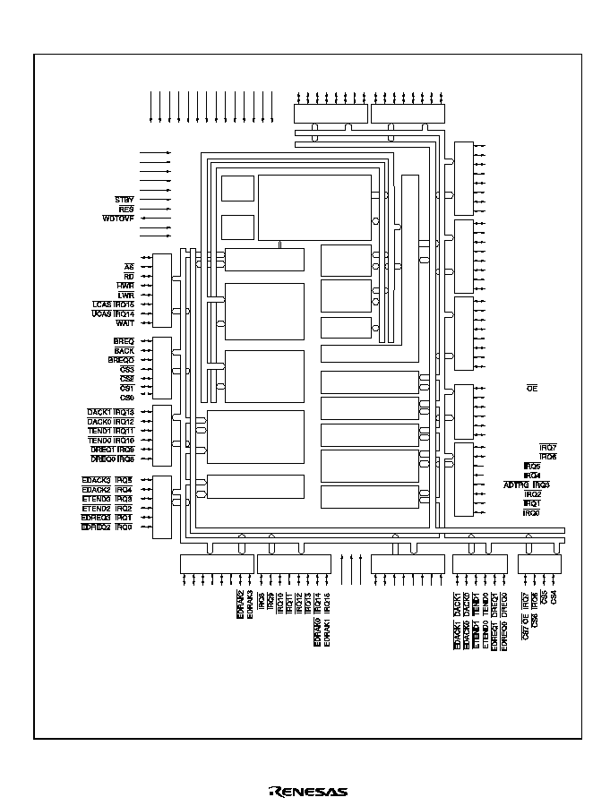
Rev. 2.0, 04/02, page 3 of 906
1.2
Block Diagram
PE7/D7
PE6/D6
PE5/D5
PE4/D4
PE3/D3
PE2/D2
PE1/D1
PE0/D0
Internal data bus
Peripheral address bus
Peripheral data bus
PD7/D15
PD6/D14
PD5/D13
PD4/D12
PD3/D11
PD2/D10
PD1/D9
PD0/D8
Port D
PLLVcc
PLLVss
Vcc
Vcc
Vcc
Vcc
Vcc
Vss
Vss
Vss
Vss
Vss
Vss
Vss
PA7 / A23
PA6 / A22
PA5 / A21
PA4 / A20
PA3 / A19
PA2 / A18
PA1 / A17
PA0 / A16
PB7 / A15
PB6 / A14
PB5 / A13
PB4 / A12
PB3 / A11
PB2 / A10
PB1 / A9
PB0 / A8
PC7 / A7
PC6 / A6
PC5 / A5
PC4 / A4
PC3 / A3
PC2 / A2
PC1 / A1
PC0 / A0
P35 / SCK1/(
)
P34 / SCK0
P33 / RxD1
P32 / RxD0/IrRxD
P31 / TxD1
P30 / TxD0/IrTxD
P57 / AN15/DA3/
P56 / AN14/DA2/
P55 / AN13/
P54 / AN12/
P53 /
//
P52 / SCK2/
P51 / RxD2/
P50 / TxD2/
P47
/
AN7
/
DA1
P46
/
AN6
/
DA0
P45
/
AN5
P44
/
AN4
P43
/
AN3
P42
/
AN2
P41
/
AN1
P40
/
AN0
Vref
AVcc
AVss
P20
/PO0
/
TIOCA3/(
)
P21
/PO1
/
TIOCB3/(
)
P22
/PO2
/
TIOCC3
/
(
)
P23
/PO3
/
TIOCD3
/
(
)
P24
/PO4
/
TIOCA4
/
(
)
P25
/PO5
/
TIOCB4
/
(
)
P26
/PO6
/
TIOCA5
/
/(
)
P27
/PO7
/
TIOCB5
/
/(
)
P10/
PO8
/
TIOCA0
P11
/
PO9
/
TIOCB0
P12
/
PO10
/
TIOCC0
/
TCLKA
P13
/
PO11
/
TIOCD0
/
TCLKB
P14
/
PO12
/
TIOCA1
P15
/
PO13
/
TIOCB1
/
TCLKC
P16
/
PO14
/
TIOCA2/
P17
/
PO15
/
TIOCB2
/
TCLKD/
P65 /TMO1/
/
P64 /TMO0/
/
P63 /TMCI1/
/
P62 /TMCI0/
/
P61 /TMRI1/
/
P60 /TMRI0/
/
PG6 /
PG5 /
PG4 /
PG3 /
PG2 /
PG1 /
PG0 /
PF7 /¯
PF6 /
PF5 /
PF4 /
PF3 /
PF2/
/
PF1 /
/
PF0 /
ROM
*
1
(Flash memory
or mask ROM)
RAM
WDT
TPU ◊ 6 channels
TMR ◊ 2 channels
SCI ◊ 3 channels
8-bit D/A converter
10-bit A/D converter
PPG
MD2
MD1
MD0
EXTAL
XTAL
FWE
*
2
NMI
H8S/2600 CPU
DTC
Interrupt controller
Port E
Port 4
P75
/
/(
)
P74
/
/(
)
P73
/
/(
)
P72
/
/(
)
P71
/
/(
)
P70
/
/(
)
Port 7
PH3/
/
/(
)
PH2/
/(
)
PH1/
PH0/
Port H
Port 2
Port 1
DMAC
EXDMAC
Internal address bus
P85 /
/(
)
P84 /
/(
)
P83 /
/(
)
P82 /
/(
)
P81 /
/(
)
P80 /
/(
)
Port 8
Bus controller
Notes:
Port 6
Port G
Port F
Port A
Port B
Port C
Port 3
Port 5
ROM is not supported in the ROMless version.
The FWE pin is used only in the F-ZTAT version. In other versions, this is an NC pin.
1.
2.
PLL
Clock
pulse
generator
Figure 1.1 H8S/2678 Series Internal Block Diagram
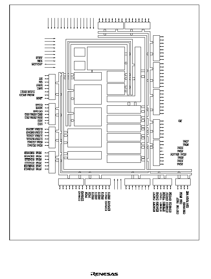
Rev. 2.0, 04/02, page 4 of 906
PE7/D7
PE6/D6
PE5/D5
PE4/D4
PE3/D3
PE2/D2
PE1/D1
PE0/D0
PD7/D15
PD6/D14
PD5/D13
PD4/D12
PD3/D11
PD2/D10
PD1/D9
PD0/D8
Vcc
Vcc
Vcc
Vcc
Vcc
PLLVcc
PLLV
ss
V
ss
V
ss
V
ss
V
ss
V
ss
V
ss
V
ss
V
ss
PA7 / A23
PA6 / A22
PA5 / A21
PA4 / A20
PA3 / A19
PA2 / A18
PA1 / A17
PA0 / A16
PB7 / A15
PB6 / A14
PB5 / A13
PB4 / A12
PB3 / A11
PB2 / A10
PB1 / A9
PB0 / A8
PC7 / A7
PC6 / A6
PC5 / A5
PC4 / A4
PC3 / A3
PC2 / A2
PC1 / A1
PC0 / A0
P35 / SCK1/(
)/(CKE)
P34 / SCK0
P33 / RxD1
P32 / RxD0/IrRxD
P31 / TxD1
P30 / TxD0/IrTxD
P57 / AN15/DA3/
P56 / AN14/DA2/
P55 / AN13/
P54 / AN12/
P53 /
//
P52 / SCK2/
P51 / RxD2/
P50 / TxD2/
P47
/
AN7
/
DA1
P46
/
AN6
/
DA0
P45
/
AN5
P44
/
AN4
P43
/
AN3
P42
/
AN2
P41
/
AN1
P40
/
AN0
Vref
AVcc
AVss
P20
/
PO0
/
TIOCA3/(
)
P21
/
PO1
/
TIOCB3/(
)
P22
/
PO2
/
TIOCC3
/
(
)
P23
/
PO3
/
TIOCD3
/
(
)
P24
/
PO4
/
TIOCA4
/
(
)
P25
/
PO5
/
TIOCB4
/
(
)
P26
/
PO6
/
TIOCA5
/
/(
)
P27
/
PO7
/
TIOCB5
/
/(
)
P10/
PO8
/
TIOCA0
P11
/
PO9
/
TIOCB0
P12
/
PO10
/
TIOCC0
/
TCLKA
P13
/
PO11
/TIOCD0
/
TCLKB
P14
/
PO12
/
TIOCA1
P15
/
PO13
/
TIOCB1
/
TCLKC
P16
/
PO14
/
TIOCA2/
P17
/
PO15
/
TIOCB2
/
TCLKD/
P65 /TMO1/
/
P64 /TMO0/
/
P63 /TMCI1/
/
P62 /TMCI0/
/
P61 / TMRI1/
/
P60 / TMRI0/
/
PG6 /
PG5 /
PG4 /
PG3 /
/
/
PG2 /
/
/
PG1 /
PG0 /
PF7 /
PF6 /
PF5 /
PF4 /
PF3 /
PF2/
/
/DQML
PF1 /
/
/DQMU
PF0 /
ROM
*
(Flash memory)
RAM
WDT
EXDMAC
TPU ◊ 6 channels
Note:
*
ROM is not supported in the ROMless version.
SCI
◊ 3 channels
PPG
Port 1
Port 2
Port 4
MD2
MD1
MD0
DCTL
EXTAL
XTAL
NMI
H8S/2600 CPU
Interrupt controller
Port D
Port E
Port A
Port B
Peripheral data bus
Peripheral address bus
Bus controller
Port C
Port 3
Port 5
DTC
P75
/
/(
)
P74
/
/(
)
P73
/
/(
)
P72
/
/(
)
P71
/
/(
)
P70
/
/(
)
PH3/
/
/(
)/CKE
PH2/
/(
)
PH1/
/
/SDRAM
PH0/
/
/
DMAC
P85 /
/(
)
P84 /
/(
)
P83 /
/(
)
P82 /
/(
)
P81 /
/(
)
P80 /
/(
)
PLL
Clock
pulse
generator
Port 8
Port 6
Port G
Port F
TMR ◊ 2 channels
8-bit D/A converter
10-bit A/D converter
Internal data bus
Internal address bus
Port H
Port 7
Figure 1.2 H8S/2678R Series Internal Block Diagram
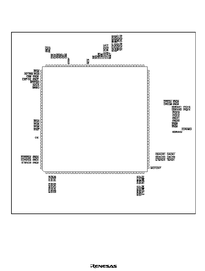
Rev. 2.0, 04/02, page 5 of 906
1.3
Pin Description
1.3.1
Pin Arrangement
MD2
P83
/
/(
)
P84
/
/(
)
P85
/
/(
)
Vcc
PC0/A0
PC1/A1
PC2/A2
PC3/A3
PC4/A4
PC5/A5
Vss
PC6/A6
PC7/A7
PB0/A8
PB1/A9
PB2/A10
PB3/A11
Vss
PB4/A12
PB5/A13
PB6/A14
PB7/A15
PA0/A16
PA1/A17
Vss
PA2/A18
PA3/A19
PA4/A20
PA5/A21
PA6/A22
PA7/A23
NC
*
2
P70
/
/(
)
P71
/
/(
)
P72
/
/(
)
P51/RxD2/
P50/TxD2/
PH1/
PH0/
PG3/
PG2/
PG1/
PG0/
Vss
XTAL
EXTAL
Vcc
PF7/
PLLVcc
PLLVss
PF6/
PF5/
PF4/
PF3/
PF2/
/
PF1/
/
PF0/
P65/TMO1/
/
P64/TMO0/
/
P63/TMCI1/
/
P62/TMCI0/
/
P
D
0/D
8
P
D
1/D
9
PD2
/
D10
PD3
/
D11
Vss
PD4
/
D12
PD5
/
D13
PD6
/
D14
108
107
106
105
104
103
102
101
100
99
98
97
96
95
94
93
92
91
90
89
88
87
86
85
84
83
82
81
80
79
78
77
76
75
74
73
P52/SCK2/
P53/
/
PH2/
/(
)
PH3/
/
/(
)
PG4 /
PG5 /
PG6 /
V c c
P40 / AN0
P41 / AN1
P42 / AN2
P43 / AN3
Vref
AVcc
P44 / AN4
P45 / AN5
P46 / AN6 / DA0
P47 / AN7 / DA1
P54 / AN12/
P55 / AN13/
P56 / AN14/DA2/
P57 / AN15/DA3/
AVss
NC
*
2
P35 / SCK1/(
)
P34 / SCK0
P33 / RxD1
Vss
P32 / RxD0/IrRxD
P31 / TxD1
P30 / TxD0/IrTxD
P80 /
/ (
)
P81 /
/ (
)
P82/
/(
)
MD0
MD1
109
110
111
112
113
114
115
116
117
118
119
120
121
122
123
124
125
126
127
128
129
130
131
132
133
134
135
136
137
138
139
140
141
142
143
144
PD7 / D15
PE0 / D0
PE1 / D1
PE2 / D2
PE3 / D3
Vcc
PE4 / D4
PE5 / D5
PE6 / D6
PE7 / D7
FWE
*
1
P61/TMRI1/
/
P60/TMRI0/
/
P27/ PO7 / TIOCB5 /
/(
)
P26/ PO6 / TIOCA5 /
/(
)
P25/ PO5 /TIOCB4 /(
)
P24/ PO4 /TIOCA4 /(
)
P23/ PO3 /TIOCD3 /(
)
P22/ PO2 /TIOCC3 /(
)
P21/PO1 /TIOCB3/(
)
P20/PO0 /TIOCA3/(
)
P17/ PO15 /TIOCB2 /TCLKD/
P16/PO14 /TIOCA2/
P15/ PO13 /TIOCB1 /TCLKC
P14/PO12 /TIOCA1
Vss
P13/ PO11 /TIOCD0 /TCLKB
P12/ PO10 /TIOCC0 /TCLKA
P11/ PO9 /TIOCB0
P10/ PO8 /TIOCA0
P75/
/(
)
P74/
/(
)
P73/
/(
)
Vcc
NMI
72
71
70
69
68
67
66
65
64
63
62
61
60
59
58
57
56
55
54
53
52
51
50
49
48
47
46
45
44
43
42
41
40
39
38
37
1
2
3
4
5
6
7
8
9
10
11
12
13
14
15
16
17
18
19
20
21
22
23
24
25
26
27
28
29
30
31
32
33
34
35
36
FP-144G
(Top view)
Notes: 1. The FWE pin is used only in the F-ZTAT version. In other versions, this is an NC pin.
2. An NC pin should be unconnected.
Figure 1.3 H8S/2678 Series Pin Arrangement
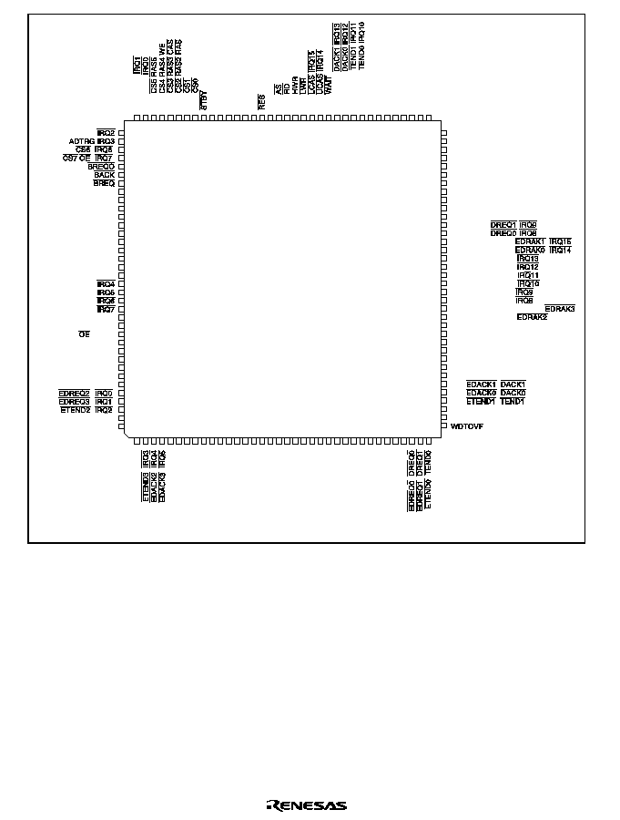
Rev. 2.0, 04/02, page 6 of 906
MD2
P83
/
/(
)
P84
/
/(
)
P85
/
/(
)
Vcc
PC0/A0
PC1/A1
PC2/A2
PC3/A3
PC4/A4
PC5/A5
Vss
PC6/A6
PC7/A7
PB0/A8
PB1/A9
PB2/A10
PB3/A11
Vss
PB4/A12
PB5/A13
PB6/A14
PB7/A15
PA0/A16
PA1/A17
Vss
PA2/A18
PA3/A19
PA4/A20
PA5/A21
PA6/A22
PA7/A23
NC
*
P70
/
/(
)
P71
/
/(
)
P72
/
/(
)
P51/RxD2/
P50/TxD2/
PH1/
/
/SDRAM
PH0/
/
/
PG3/
/
/
PG2/
/
/
PG1/
PG0/
Vss
XTAL
EXTAL
Vcc
PF7/
PLLVcc
PLLVss
PF6/
PF5/
PF4/
PF3/
PF2/
/
/DQML
PF1/
/
/DQMU
PF0/
P65/TMO1/
/
P64/TMO0/
/
P63/TMCI1/
/
P62/TMCI0/
/
P
D
0/D
8
P
D
1/D
9
PD2
/
D10
PD3
/
D11
Vss
PD4
/
D12
PD5
/
D13
PD6
/
D14
108
107
106
105
104
103
102
101
100
99
98
97
96
95
94
93
92
91
90
89
88
87
86
85
84
83
82
81
80
79
78
77
76
75
74
73
P52/SCK2/
P53/
/
PH2/
/(
)
PH3/
/
/(
)
PG4 /
PG5 /
PG6 /
V c c
P40 / AN0
P41 / AN1
P42 / AN2
P43 / AN3
Vref
AVcc
P44 / AN4
P45 / AN5
P46 / AN6 / DA0
P47 / AN7 / DA1
P54 / AN12/
P55 / AN13/
P56 / AN14/DA2/
P57 / AN15/DA3/
AVss
DCTL
P35 / SCK1/(
)/(CKE)
P34 / SCK0
P33 / RxD1
Vss
P32 / RxD0/IrRxD
P31 / TxD1
P30 / TxD0/IrTxD
P80 /
/ (
)
P81 /
/ (
)
P82/
/(
)
MD0
MD1
109
110
111
112
113
114
115
116
117
118
119
120
121
122
123
124
125
126
127
128
129
130
131
132
133
134
135
136
137
138
139
140
141
142
143
144
PD7 / D15
PE0 / D0
PE1 / D1
PE2 / D2
PE3 / D3
Vcc
PE4 / D4
PE5 / D5
PE6 / D6
PE7 / D7
Vss
P61/TMRI1/
/
P60/TMRI0/
/
P27/ PO7 / TIOCB5 /
/(
)
P26/ PO6 / TIOCA5 /
/(
)
P25/ PO5 /TIOCB4 /(
)
P24/ PO4 /TIOCA4 /(
)
P23/ PO3 /TIOCD3 /(
)
P22/ PO2 /TIOCC3 /(
)
P21/PO1 /TIOCB3/(
)
P20/PO0 /TIOCA3/(
)
P17/ PO15 /TIOCB2 /TCLKD/
P16/PO14 /TIOCA2/
P15/ PO13 /TIOCB1 /TCLKC
P14/PO12 /TIOCA1
Vss
P13/ PO11 /TIOCD0 /TCLKB
P12/ PO10 /TIOCC0 /TCLKA
P11/ PO9 /TIOCB0
P10/ PO8 /TIOCA0
P75/
/(
)
P74/
/(
)
P73/
/(
)
Vcc
NMI
72
71
70
69
68
67
66
65
64
63
62
61
60
59
58
57
56
55
54
53
52
51
50
49
48
47
46
45
44
43
42
41
40
39
38
37
1
2
3
4
5
6
7
8
9
10
11
12
13
14
15
16
17
18
19
20
21
22
23
24
25
26
27
28
29
30
31
32
33
34
35
36
FP-144H
(Top view)
Note:
An NC pin should be unconnected.
Figure 1.4 H8S/2678R Series Pin Arrangement

Rev. 2.0, 04/02, page 7 of 906
1.3.2
Pin Arrangement in Each Operating Mode
Table 1.1
Pin Arrangement in Each Operating Mode
Pin Name
Pin
No.
Mode 7
Modes 1 and 5
Modes 2 and 6
Mode 4
EXPE = 1
EXPE = 0
Flash Memory
Programmer
Mode
1
MD2
MD2
MD2
MD2
MD2
Vss
2
P83/
(7(1'
/
(
,54
)
P83/
(7(1'
/
(
,54
)
P83/
(7(1'
/
(
,54
)
P83/
(7(1'
/
(
,54
)
P83/(
,54
)
NC
3
P84/
('$&.
/
(
,54
)
P84/
('$&.
/
(
,54
)
P84/
('$&.
/
(
,54
)
P84/
('$&.
/
(
,54
)
P84/(
,54
)
NC
4
P85/
('$&.
/
(
,54
)
P85/
('$&.
/
(
,54
)
P85/
('$&.
/
(
,54
)
P85/
('$&.
/
(
,54
)
P85/(
,54
)
NC
5
Vcc
Vcc
Vcc
Vcc
Vcc
Vcc
6
A0
A0
PC0/A0
PC0/A0
PC0
A0
7
A1
A1
PC1/A1
PC1/A1
PC1
A1
8
A2
A2
PC2/A2
PC2/A2
PC2
A2
9
A3
A3
PC3/A3
PC3/A3
PC3
A3
10
A4
A4
PC4/A4
PC4/A4
PC4
A4
11
A5
A5
PC5/A5
PC5/A5
PC5
A5
12
Vss
Vss
Vss
Vss
Vss
Vss
13
A6
A6
PC6/A6
PC6/A6
PC6
A6
14
A7
A7
PC7/A7
PC7/A7
PC7
A7
15
A8
A8
PB0/A8
PB0/A8
PB0
A8
16
A9
A9
PB1/A9
PB1/A9
PB1
A9
17
A10
A10
PB2/A10
PB2/A10
PB2
A10
18
A11
A11
PB3/A11
PB3/A11
PB3
A11
19
Vss
Vss
Vss
Vss
Vss
Vss
20
A12
A12
PB4/A12
PB4/A12
PB4
A12
21
A13
A13
PB5/A13
PB5/A13
PB5
A13
22
A14
A14
PB6/A14
PB6/A14
PB6
A14
23
A15
A15
PB7/A15
PB7/A15
PB7
A15
24
A16
A16
PA0/A16
PA0/A16
PA0
A16
25
A17
A17
PA1/A17
PA1/A17
PA1
A17
26
Vss
Vss
Vss
Vss
Vss
Vss
27
A18
A18
PA2/A18
PA2/A18
PA2
A18

Rev. 2.0, 04/02, page 8 of 906
Pin Name
Pin
No.
Mode 7
Modes 1 and 5
Modes 2 and 6
Mode 4
EXPE = 1
EXPE = 0
Flash Memory
Programmer
Mode
28
A19
A19
PA3/A19
PA3/A19
PA3
NC
29
A20
A20
PA4/A20
PA4/A20
PA4
NC
30
PA5/A21
PA5/A21
PA5/A21
PA5/A21
PA5
NC
31
PA6/A22
PA6/A22
PA6/A22
PA6/A22
PA6
NC
32
PA7/A23
PA7/A23
PA7/A23
PA7/A23
PA7
NC
33
NC
NC
NC
NC
NC
NC
34
P70/
('5(4
/
(
'5(4
)
P70/
('5(4
/
(
'5(4
)
P70/
('5(4
/
(
'5(4
)
P70/
('5(4
/
(
'5(4
)
P70/(
'5(4
)
NC
35
P71/
('5(4
/
(
'5(4
)
P71/
('5(4
/
(
'5(4
)
P71/
('5(4
/
(
'5(4
)
P71/
('5(4
/
(
'5(4
)
P71/(
'5(4
)
NC
36
P72/
(7(1'
/
(
7(1'
)
P72/
(7(1'
/
(
7(1'
)
P72/
(7(1'
/
(
7(1'
)
P72/
(7(1'
/
(
7(1'
)
P72/(
7(1'
)
NC
37
:'729)
:'729)
:'729)
:'729)
:'729)
NC
38
NMI
NMI
NMI
NMI
NMI
Vcc
39
Vcc
Vcc
Vcc
Vcc
Vcc
Vcc
40
P73/
(7(1'
/
(
7(1'
)
P73/
(7(1'
/
(
7(1'
)
P73/
(7(1'
/
(
7(1'
)
P73/
(7(1'
/
(
7(1'
)
P73/(
7(1'
)
NC
41
P74/
('$&.
/
(
'$&.
)
P74/
('$&.
/
(
'$&.
)
P74/
('$&.
/
(
'$&.
)
P74/
('$&.
/
(
'$&.
)
P74/(
'$&.
)
NC
42
P75/
('$&.
/
(
'$&.
)
P75/
('$&.
/
(
'$&.
)
P75/
('$&.
/
(
'$&.
)
P75/
('$&.
/
(
'$&.
)
P75/(
'$&.
)
NC
43
P10/PO8/TIOCA0
P10/PO8/TIOCA0
P10/PO8/TIOCA0
P10/PO8/TIOCA0
P10/PO8/TIOCA0
NC
44
P11/PO9/TIOCB0
P11/PO9/TIOCB0
P11/PO9/TIOCB0
P11/PO9/TIOCB0
P11/PO9/TIOCB0
NC
45
P12/PO10/
TIOCC0/TCLKA
P12/PO10/
TIOCC0/TCLKA
P12/PO10/
TIOCC0/TCLKA
P12/PO10/
TIOCC0/TCLKA
P12/PO10/
TIOCC0/TCLKA
NC
46
P13/PO11/
TIOCD0/TCLKB
P13/PO11/
TIOCD0/TCLKB
P13/PO11/
TIOCD0/TCLKB
P13/PO11/
TIOCD0/TCLKB
P13/PO11/
TIOCD0/TCLKB
NC
47
Vss
Vss
Vss
Vss
Vss
Vss
48
P14/PO12/
TIOCA1
P14/PO12/
TIOCA1
P14/PO12/
TIOCA1
P14/PO12/
TIOCA1
P14/PO12/
TIOCA1
NC
49
P15/PO13/
TIOCB1/TCLKC
P15/PO13/
TIOCB1/TCLKC
P15/PO13/
TIOCB1/TCLKC
P15/PO13/
TIOCB1/TCLKC
P15/PO13/
TIOCB1/TCLKC
NC
50
P16/PO14/
TIOCA2/
('5$.
P16/PO14/
TIOCA2/
('5$.
P16/PO14/
TIOCA2/
('5$.
P16/PO14/
TIOCA2/
('5$.
P16/PO14/
TIOCA2
NC

Rev. 2.0, 04/02, page 9 of 906
Pin Name
Pin
No.
Mode 7
Modes 1 and 5
Modes 2 and 6
Mode 4
EXPE = 1
EXPE = 0
Flash Memory
Programmer
Mode
51
P17/PO15/
TIOCB2/TCLKD/
('5$.
P17/PO15/
TIOCB2/TCLKD/
('5$.
P17/PO15/
TIOCB2/TCLKD/
('5$.
P17/PO15/
TIOCB2/TCLKD/
('5$.
P17/PO15/
TIOCB2/TCLKD
NC
52
P20/PO0/
TIOCA3/(
,54
)
P20/PO0/
TIOCA3/(
,54
)
P20/PO0/
TIOCA3/(
,54
)
P20/PO0/
TIOCA3/(
,54
)
P20/PO0/
TIOCA3/(
,54
)
NC
53
P21/PO1/
TIOCB3/(
,54
)
P21/PO1/
TIOCB3/(
,54
)
P21/PO1/
TIOCB3/(
,54
)
P21/PO1/
TIOCB3/(
,54
)
P21/PO1/
TIOCB3/(
,54
)
NC
54
P22/PO2/
TIOCC3/(
,54
)
P22/PO2/
TIOCC3/(
,54
)
P22/PO2/
TIOCC3/(
,54
)
P22/PO2/
TIOCC3/(
,54
)
P22/PO2/
TIOCC3/(
,54
)
2(
55
P23/PO3/
TIOCD3/(
,54
)
P23/PO3/
TIOCD3/(
,54
)
P23/PO3/
TIOCD3/(
,54
)
P23/PO3/
TIOCD3/(
,54
)
P23/PO3/
TIOCD3/(
,54
)
&(
56
P24/PO4/
TIOCA4/(
,54
)
P24/PO4/
TIOCA4/(
,54
)
P24/PO4/
TIOCA4/(
,54
)
P24/PO4/
TIOCA4/(
,54
)
P24/PO4/
TIOCA4/(
,54
)
:(
57
P25/PO5/
TIOCB4/(
,54
)
P25/PO5/
TIOCB4/(
,54
)
P25/PO5/
TIOCB4/(
,54
)
P25/PO5/
TIOCB4/(
,54
)
P25/PO5/
TIOCB4/(
,54
)
Vss
58
P26/PO6/
TIOCA5/
('5$.
/(
,54
)
P26/PO6/
TIOCA5/
('5$.
/(
,54
)
P26/PO6/
TIOCA5/
('5$.
/(
,54
)
P26/PO6/
TIOCA5/
('5$.
/(
,54
)
P26/PO6/
TIOCA5/(
,54
)
NC
59
P27/PO7/
TIOCB5/
('5$.
/(
,54
)
P27/PO7/
TIOCB5/
('5$.
/(
,54
)
P27/PO7/
TIOCB5/
('5$.
/(
,54
)
P27/PO7/
TIOCB5/
('5$.
/(
,54
)
P27/PO7/
TIOCB5/(
,54
)
NC
60
P60/TMRI0/
'5(4
/
,54
P60/TMRI0/
'5(4
/
,54
P60/TMRI0/
'5(4
/
,54
P60/TMRI0/
'5(4
/
,54
P60/TMRI0/
'5(4
/
,54
NC
61
P61/TMRI1/
'5(4
/
,54
P61/TMRI1/
'5(4
/
,54
P61/TMRI1/
'5(4
/
,54
P61/TMRI1/
'5(4
/
,54
P61/TMRI1/
'5(4
/
,54
NC
62
FWE
*
1
Vss
*
2
FWE
*
1
Vss
*
2
FWE
*
1
Vss
*
2
FWE
*
1
Vss
*
2
FWE
*
1
Vss
*
2
FWE
*
1
Vss
*
2
63
D7
PE7/D7
PE7/D7
PE7/D7
PE7
NC
64
D6
PE6/D6
PE6/D6
PE6/D6
PE6
NC
65
D5
PE5/D5
PE5/D5
PE5/D5
PE5
NC
66
D4
PE4/D4
PE4/D4
PE4/D4
PE4
NC
67
Vcc
Vcc
Vcc
Vcc
Vcc
Vcc
68
D3
PE3/D3
PE3/D3
PE3/D3
PE3
NC
69
D2
PE2/D2
PE2/D2
PE2/D2
PE2
NC
70
D1
PE1/D1
PE1/D1
PE1/D1
PE1
NC
71
D0
PE0/D0
PE0/D0
PE0/D0
PE0
NC
72
D15
D15
D15
D15
PD7
I/O7

Rev. 2.0, 04/02, page 10 of 906
Pin Name
Pin
No.
Mode 7
Modes 1 and 5
Modes 2 and 6
Mode 4
EXPE = 1
EXPE = 0
Flash Memory
Programmer
Mode
73
D14
D14
D14
D14
PD6
I/O6
74
D13
D13
D13
D13
PD5
I/O5
75
D12
D12
D12
D12
PD4
I/O4
76
Vss
Vss
Vss
Vss
Vss
Vss
77
D11
D11
D11
D11
PD3
I/O3
78
D10
D10
D10
D10
PD2
I/O2
79
D9
D9
D9
D9
PD1
I/O1
80
D8
D8
D8
D8
PD0
I/O0
81
P62/TMCI0/
7(1'
/
,54
P62/TMCI0/
7(1'
/
,54
P62/TMCI0/
7(1'
/
,54
P62/TMCI0/
7(1'
/
,54
P62/TMCI0/
7(1'
/
,54
NC
82
P63/TMCI1/
7(1'
/
,54
P63/TMCI1/
7(1'
/
,54
P63/TMCI1/
7(1'
/
,54
P63/TMCI1/
7(1'
/
,54
P63/TMCI1/
7(1'
/
,54
NC
83
P64/TMO0/
'$&.
/
,54
P64/TMO0/
'$&.
/
,54
P64/TMO0/
'$&.
/
,54
P64/TMO0/
'$&.
/
,54
P64/TMO0/
'$&.
/
,54
NC
84
P65/TMO1/
'$&.
/
,54
P65/TMO1/
'$&.
/
,54
P65/TMO1/
'$&.
/
,54
P65/TMO1/
'$&.
/
,54
P65/TMO1/
'$&.
/
,54
NC
85
PF0/
:$,7
PF0/
:$,7
PF0/
:$,7
PF0/
:$,7
PF0
NC
86
PF1/
8&$6
/
,54
/DQMU
*
2
PF1/
8&$6
/
,54
/DQMU
*
2
PF1/
8&$6
/
,54
/DQMU
*
2
PF1/
8&$6
/
,54
/DQMU
*
2
PF1/
,54
NC
87
PF2/
/&$6
/
,54
/DQML
*
2
PF2/
/&$6
/
,54
/DQML
*
2
PF2/
/&$6
/
,54
/DQML
*
2
PF2/
/&$6
/
,54
/DQML
*
2
PF2/
,54
NC
88
PF3/
/:5
PF3/
/:5
PF3/
/:5
PF3/
/:5
PF3
NC
89
+:5
+:5
+:5
+:5
PF4
NC
90
5'
5'
5'
5'
PF5
NC
91
PF6/
$6
PF6/
$6
PF6/
$6
PF6/
$6
PF6
NC
92
PLLVss
PLLVss
PLLVss
PLLVss
PLLVss
Vss
93
5(6
5(6
5(6
5(6
5(6
5(6
94
PLLVcc
PLLVcc
PLLVcc
PLLVcc
PLLVcc
Vcc
95
PF7/
PF7/
PF7/
PF7/
PF7/
NC
96
Vcc
Vcc
Vcc
Vcc
Vcc
Vcc
97
EXTAL
EXTAL
EXTAL
EXTAL
EXTAL
EXTAL
98
XTAL
XTAL
XTAL
XTAL
XTAL
XTAL
99
Vss
Vss
Vss
Vss
Vss
Vss
100
67%<
67%<
67%<
67%<
67%<
Vcc

Rev. 2.0, 04/02, page 11 of 906
Pin Name
Pin
No.
Mode 7
Modes 1 and 5
Modes 2 and 6
Mode 4
EXPE = 1
EXPE = 0
Flash Memory
Programmer
Mode
101
PG0/
&6
PG0/
&6
PG0/
&6
PG0/
&6
PG0
NC
102
PG1/
&6
PG1/
&6
PG1/
&6
PG1/
&6
PG1
NC
103
PG2/
&6
/
5$6*
2
/
5$6*
2
PG2/
&6
/
5$6*
2
/
5$6*
2
PG2/
&6
/
5$6*
2
/
5$6*
2
PG2/
&6
/
5$6*
2
/
5$6*
2
PG2
NC
104
PG3/
&6
/
5$6*
2
/
&$6*
2
PG3/
&6
/
5$6*
2
/
&$6*
2
PG3/
&6
/
5$6*
2
/
&$6*
2
PG3/
&6
/
5$6*
2
/
&$6*
2
PG3
NC
105
PH0/
&6
/
5$6*
2
/
:(*
2
PH0/
&6
/
5$6*
2
/
:(*
2
PH0/
&6
/
5$6*
2
/
:(*
2
PH0/
&6
/
5$6*
2
/
:(*
2
PH0
NC
106
PH1/
&6
/
5$6*
2
/
SDRAM
*
2
PH1/
&6
/
5$6*
2
/
SDRAM
*
2
PH1/
&6
/
5$6*
2
/
SDRAM
*
2
PH1/
&6
/
5$6*
2
/
SDRAM
*
2
PH1
NC
107
P50/TxD2/
,54
P50/TxD2/
,54
P50/TxD2/
,54
P50/TxD2/
,54
P50/TxD2/
,54
Vss
108
P51/RxD2/
,54
P51/RxD2/
,54
P51/RxD2/
,54
P51/RxD2/
,54
P51/RxD2/
,54
Vss
109
P52/SCK2/
,54
P52/SCK2/
,54
P52/SCK2/
,54
P52/SCK2/
,54
P52/SCK2/
,54
Vcc
110
P53/
$'75*
/
,54
P53/
$'75*
/
,54
P53/
$'75*
/
,54
P53/
$'75*
/
,54
P53/
$'75*
/
,54
NC
111
PH2/
&6
/(
,54
)
PH2/
&6
/(
,54
)
PH2/
&6
/(
,54
)
PH2/
&6
/(
,54
)
PH2/(
,54
∑
NC
112
PH3/
&6
/
2(
/
(
,54
)/CKE
*
2
PH3/
&6
/
2(
/
(
,54
)/CKE
*
2
PH3/
&6
/
2(
/
(
,54
)/CKE
*
2
PH3/
&6
/
2(
/
(
,54
)/CKE
*
2
PH3/(
,54
)
NC
113
PG4/
%5(42
PG4/
%5(42
PG4/
%5(42
PG4/
%5(42
PG4
NC
114
PG5/
%$&.
PG5/
%$&.
PG5/
%$&.
PG5/
%$&.
PG5
NC
115
PG6/
%5(4
PG6/
%5(4
PG6/
%5(4
PG6/
%5(4
PG6
NC
116
Vcc
Vcc
Vcc
Vcc
Vcc
Vcc
117
P40/AN0
P40/AN0
P40/AN0
P40/AN0
P40/AN0
NC
118
P41/AN1
P41/AN1
P41/AN1
P41/AN1
P41/AN1
NC
119
P42/AN2
P42/AN2
P42/AN2
P42/AN2
P42/AN2
NC
120
P43/AN3
P43/AN3
P43/AN3
P43/AN3
P43/AN3
NC
121
Vref
Vref
Vref
Vref
Vref
NC
122
AVcc
AVcc
AVcc
AVcc
AVcc
Vcc
123
P44/AN4
P44/AN4
P44/AN4
P44/AN4
P44/AN4
NC
124
P45/AN5
P45/AN5
P45/AN5
P45/AN5
P45/AN5
NC
125
P46/AN6/DA0
P46/AN6/DA0
P46/AN6/DA0
P46/AN6/DA0
P46/AN6/DA0
NC
126
P47/AN7/DA1
P47/AN7/DA1
P47/AN7/DA1
P47/AN7/DA1
P47/AN7/DA1
NC
127
P54/AN12/
,54
P54/AN12/
,54
P54/AN12/
,54
P54/AN12/
,54
P54/AN12/
,54
NC

Rev. 2.0, 04/02, page 12 of 906
Pin Name
Pin
No.
Mode 7
Modes 1 and 5
Modes 2 and 6
Mode 4
EXPE = 1
EXPE = 0
Flash Memory
Programmer
Mode
128
P55/AN13/
,54
P55/AN13/
,54
P55/AN13/
,54
P55/AN13/
,54
P55/AN13/
,54
NC
129
P56/AN14/DA2/
,54
P56/AN14/DA2/
,54
P56/AN14/DA2/
,54
P56/AN14/DA2/
,54
P56/AN14/DA2/
,54
NC
130
P57/AN15/DA3/
,54
P57/AN15/DA3/
,54
P57/AN15/DA3/
,54
P57/AN15/DA3/
,54
P57/AN15/DA3/
,54
NC
131
AVss
AVss
AVss
AVss
AVss
Vss
132
NC
*
3
DCTL
*
2
NC
*
3
DCTL
*
2
NC
*
3
DCTL
*
2
NC
*
3
DCTL
*
2
NC
*
3
DCTL
*
2
NC
*
3
Vss
*
2
133
P35/SCK1/(
2(
)/
(CKE)
*
2
P35/SCK1/(
2(
)/
(CKE)
*
2
P35/SCK1/(
2(
)/
(CKE)
*
2
P35/SCK1/(
2(
)/
(CKE)
*
2
P35/SCK1
NC
134
P34/SCK0
P34/SCK0
P34/SCK0
P34/SCK0
P34/SCK0
NC
135
P33/RxD1
P33/RxD1
P33/RxD1
P33/RxD1
P33/RxD1
NC
136
Vss
Vss
Vss
Vss
Vss
Vss
137
P32/RxD0/IrRxD
P32/RxD0/IrRxD
P32/RxD0/IrRxD
P32/RxD0/IrRxD
P32/RxD0/IrRxD
Vcc
138
P31/TxD1
P31/TxD1
P31/TxD1
P31/TxD1
P31/TxD1
NC
139
P30/TxD0/IrTxD
P30/TxD0/IrTxD
P30/TxD0/IrTxD
P30/TxD0/IrTxD
P30/TxD0/IrTxD
NC
140
P80/
('5(4
/
(
,54
)
P80/
('5(4
/
(
,54
)
P80/
('5(4
/
(
,54
)
P80/
('5(4
/
(
,54
)
P80/(
,54
)
NC
141
P81/
('5(4
/
(
,54
)
P81/
('5(4
/
(
,54
)
P81/
('5(4
/
(
,54
)
P81/
('5(4
/
(
,54
)
P81/(
,54
)
NC
142
P82/
(7(1'
/
(
,54
)
P82/
(7(1'
/
(
,54
)
P82/
(7(1'
/
(
,54
)
P82/
(7(1'
/
(
,54
)
P82/(
,54
)
NC
143
MD0
MD0
MD0
MD0
MD0
Vss
144
MD1
MD1
MD1
MD1
MD1
Vss
Notes:
*
1 The FWE pin is used only in the flash memory version of the H8S/2678 Series. In the
masked ROM and ROMless
versions of the H8S/2678 Series, this is an NC pin.
*
2 Only for the H8S/2678R Series.
*
3 Only for the H8S/2678 Series.

Rev. 2.0, 04/02, page 13 of 906
1.3.3
Pin Functions
Table 1.2
Pin Functions
Pin No.
Type
Symbol
FP-144G
(H8S/2678
Series)
FP-144H
(H8S/2678R
Series)
I/O
Function
Power
V
CC
5, 39, 67,
96, 116
5, 39, 67,
96, 116
Input
For connection to the power supply.
All V
CC
pins should be connected to
the system power supply.
V
SS
12, 19, 26,
47, 76, 99,
136
12, 19, 26,
47, 76, 99,
136
Input
For connection to ground. All V
SS
pins should be connected to the
system power supply (0 V).
PLLV
CC
94
94
Input
Power supply pin for the on-chip PLL
oscillator.
PLLV
SS
92
92
Input
Ground pin for the on-chip PLL
oscillator.
Clock
XTAL
98
98
Input
For connection to a crystal oscillator.
See section 21, Clock Pulse
Generator for typical connection
diagrams for a crystal oscillator and
external clock input.
EXTAL
97
97
Input
For connection to a crystal oscillator.
The EXTAL pin can also input an
external clock. See section 21, Clock
Pulse Generator for typical
connection diagrams for a crystal
oscillator and external clock input.
95
95
Output Supplies the system clock to
external devices.
SDRAM
--
106
Output When a synchronous DRAM is
connected, this pin is connected to
the CLK pin of the synchronous
DRAM. For details, refer to section
6, Bus Controller.
Operating
mode control
MD2
MD1
MD0
1, 144, 143 1, 144, 143
Input
These pins set the operating mode.
These pins should not be changed
while the MCU is operating.

Rev. 2.0, 04/02, page 14 of 906
Pin No.
Type
Symbol
FP-144G
(H8S/2678
Series)
FP-144H
(H8S/2678R
Series)
I/O
Function
Operating
mode control
DCTL
--
132
Input
When this pin is driven high,
SDRAM
dedicated to the
synchronous DRAM is output.
When not using the synchronous
DRAM interface, drive this pin low.
The level of this pin must not be
changed during operation.
System control
5(6
93
93
Input
When this pin is driven low, the chip
is reset.
67%<
100
100
Input
When this pin is driven low, a
transition is made to hardware
standby mode.
%5(4
115
115
Input
Requests chip to release the bus to
an external bus master.
%5(42
113
113
Output External bus request signal used
when an internal bus master
accesses external space when the
external bus is released.
%$&.
114
114
Output Indicates that the bus has been
released to an external bus master.
FWE
62
--
Input
Enables/disables flash memory. This
pin is only used in the flash memory
version.
Address bus
A23 to A0 32 to 27,
25 to 20,
18 to 13,
11 to 6
32 to 27,
25 to 20,
18 to 13,
11 to 6
Output These pins output an address.
Data bus
D15 to
D0
72 to 75,
77 to 80,
63 to 66,
68 to 71
72 to 75,
77 to 80,
63 to 66,
68 to 71
Input/
output
These pins constitute a bidirectional
data bus.
Bus control
&6
to
&6
112, 111,
106 to 101
112, 111,
106 to 101
Output Signals that select division areas 7
to 0 in the external address space.
$6
91
91
Output When this pin is low, it indicates that
address output on the address bus is
valid.
5'
90
90
Output When this pin is low, it indicates that
the external address space is being
read.

Rev. 2.0, 04/02, page 15 of 906
Pin No.
Type
Symbol
FP-144G
(H8S/2678
Series)
FP-144H
(H8S/2678R
Series)
I/O
Function
Bus control
+:5
89
89
Output Strobe signal indicating that external
address space is to be written, and
the upper half (D15 to D8) of the
data bus is enabled.
Write enable signal for DRAM
interface space.
/:5
88
88
Output Strobe signal indicating that external
address space is to be written, and
the lower half (D7 to D0) of the data
bus is enabled.
8&$6
86
86
Output Upper column address strobe signal
for 16-bit DRAM interface space.
Column address strobe signal for 8-
bit DRAM interface space.
/&$6
87
87
Output Lower column address strobe signal
for 16-bit DRAM interface space.
DQMU
--
86
Output Upper data mask enable signal for
16-bit synchronous DRAM for 16-bit
synchronous DRAM interface.
Data mask enable signal for 8-bit
synchronous DRAM interface space.
DQML
--
87
Output Lower-data mask enable signal for
16-bit synchronous DRAM interface
space.
5$6
/
5$6
5$6
to
5$6
--
103 to 106
Output Row address strobe signal for the
synchronous DRAM interface.
5$6
signal is a row address strobe
signal when areas 2 to 5 are set to
the continuous DRAM space.
5$6
--
103
Row address strobe signal for the
synchronous DRAM of the
synchronous DRAM interface.
&$6
--
104
Output Column address strobe signal for the
synchronous DRAM of the
synchronous DRAM interface.
:(
--
105
Output Write enable signal for the
synchronous DRAM of the
synchronous DRAM interface.

Rev. 2.0, 04/02, page 16 of 906
Pin No.
Type
Symbol
FP-144G
(H8S/2678
Series)
FP-144H
(H8S/2678R
Series)
I/O
Function
Bus control
:$,7
85
85
Input
Requests insertion of a wait state in
the bus cycle when accessing
external 3-state address space.
2(
(
2(
)
112, 133
112, 133
Output Output enable signal for DRAM
interface space.
The output pins of
2(
and (
2(
) are
selected by the port function control
register 2 (PFCR2) of port 3.
CKE
(CKE)
--
112, 133
Output Clock enable signal of the
synchronous DRAM interface space.
The output pins of CKE and (
&.(
)
are selected by the port function
control register 2 (PFCR2) of port 3.
Interrupt
signals
NMI
38
38
Input
Nonmaskable interrupt request pin.
Fix high when not used.
,54
to
,54
87, 86,
84 to 81,
61, 60,
130 to 127,
110 to 107
87, 86,
84 to 81,
61, 60,
130 to 127,
110 to 107
(
,54
)
to (
,54
)
59 to 52,
112, 111,
4 to 2,
142 to 140
59 to 52,
112, 111,
4 to 2,
142 to 140
Input
These pins request a maskable
interrupt.
The input pins of
'5(4Q
and
(
'5(4Q
) are selected by the IRQ
pin select register (ITSR) of the
interrupt controller. (n = 0 to 15)
DMA controller
(DMAC)
'5(4
'5(4
(
'5(4
)
(
'5(4
)
61, 60, 35,
34
61, 60, 35,
34
Input
These signals request DMAC
activation.
The input pins of
'5(4Q
and
(
'5(4Q
) are selected by the IRQ
pin select register (ITSR) of the
interrupt controller. (n = 0 to 15)
7(1'
7(1'
(
7(1'
)
(
7(1'
)
82, 81, 40,
36
82, 81, 40,
36
Output These signals indicate the end of
DMAC data transfer.
The input pins of
7(1'Q
and
(
7(1'Q
) are selected by the port
function control register 2 (PFCR2)
of port 3. (n = 1, 0)

Rev. 2.0, 04/02, page 17 of 906
Pin No.
Type
Symbol
FP-144G
(H8S/2678
Series)
FP-144H
(H8S/2678R
Series)
I/O
Function
DMA controller
(DMAC)
'$&.
'$&.
(
'$&.
)
(
'$&.
)
84, 83, 42,
41
84, 83, 42,
41
Output DMAC single address transfer
acknowledge signals.
The input pins of
'$&.Q
and
(
'$&.Q
) are selected by the port
function control register 2 (PFCR2)
of port 3. (n = 1, 0)
EXDMA
controller
(EXDMAC)
('5(4
to
('5(4
141, 140,
35, 34
141, 140,
35, 34
Input
These signals request EXDMAC
activation.
(7(1'
to
(7(1'
2, 142, 40,
36
2, 142, 40,
36
Output These signals indicate the end of
EXDMAC data transfer.
('$&.
to
('$&.
4, 3, 42, 41 4, 3, 42, 41
Output EXDMAC single address transfer
acknowledge signals.
('5$.
to
('5$.
51, 50, 59,
58
51, 50, 59,
58
Output These signals notify an external
device of acceptance and start of
execution of a DMA transfer request.
16-bit timer
pulse unit
(TPU)
TCLKA
TCLKB
TCLKC
TCLKD
45, 46, 49,
51
45, 46, 49,
51
Input
External clock input pins.
TIOCA0
TIOCB0
TIOCC0
TIOCD0
43, 44, 45,
46
43, 44, 45,
46
Input/
output
TGRA_0 to TGRD_0 input capture
input/output compare output/PWM
output pins.
TIOCA1
TIOCB1
48, 49
48, 49
Input/
output
TGRA_1 and TGRB_1 input capture
input/output compare output/PWM
output pins.
TIOCA2
TIOCB2
50, 51
50, 51
Input/
output
TGRA_2 and TGRB_2 input capture
input/output compare output/PWM
output pins.
TIOCA3
TIOCB3
TIOCC3
TIOCD3
52, 53, 54,
55
52, 53, 54,
55
Input/
output
TGRA_3 to TGRD_3 input capture
input/output compare output/PWM
output pins.
TIOCA4
TIOCB4
56, 57
56, 57
Input/
output
TGRA_4 and TGRB_4 input capture
input/output compare output/PWM
output pins.

Rev. 2.0, 04/02, page 18 of 906
Pin No.
Type
Symbol
FP-144G
(H8S/2678
Series)
FP-144H
(H8S/2678R
Series)
I/O
Function
16-bit timer
pulse unit
(TPU)
TIOCA5,
TIOCB5
58, 59
58, 59
Input/
output
TGRA_5 and TGRB_5 input capture
input/output compare output/PWM
output pins.
Programmable
pulse
generator
(PPG)
PO15 to
PO0
51 to 48,
46 to 43,
59 to 52
51 to 48,
46 to 43,
59 to 52
Output Pulse output pins.
8-bit timer
TMO0
TMO1
83, 84
83, 84
Output Waveform output pins with output
compare function.
TMCI0
TMCI1
81, 82
81, 82
Input
External event input pins.
TMRI0
TMRI1
60, 61
60, 61
Input
Counter reset input pins.
Watchdog
timer (WDT)
:'729)
37
37
Output Counter overflow signal output pin in
watchdog timer mode.
TxD2
TxD1
TxD0/IrTx
D
107, 138,
139
107, 138,
139
Output Data output pins.
Serial commu-
nication
interface
(SCI)/smart
card interface
(SCI_0 with
IrDA function)
RxD2
RxD1
RxD0/
IrRxD
108, 135,
137
108, 135,
137
Input
Data input pins.
SCK2
SCK1
SCK0
109, 133,
134
109, 133,
134
Input/
output
Clock input/output pins.
A/D converter
AN15 to
AN12,
AN7 to
AN0
130 to 127,
126 to 123,
120 to 117
130 to 127,
126 to 123,
120 to 117
Input
Analog input pins for the A/D
converter.
$'75*
110
110
Input
Pin for input of an external trigger to
start A/D conversion.
D/A converter
DA3 to
DA0
130, 129,
126, 125
130, 129,
126, 125
Output Analog input pins for the D/A
converter.
A/D converter,
D/A converter
AV
CC
122
122
Input
The analog power-supply pin for the
A/D converter and D/A converter.
When the A/D converter and D/A
converter are not used, this pin
should be connected to the system
power supply (+3 V).

Rev. 2.0, 04/02, page 19 of 906
Pin No.
Type
Symbol
FP-144G
(H8S/2678
Series)
FP-144H
(H8S/2678R
Series)
I/O
Function
A/D converter,
D/A converter
AV
SS
131
131
Input
The ground pin for the A/D converter
and D/A converter.
This pin should be connected to the
system power supply (0 V).
Vref
121
121
Input
The reference voltage input pin for
the A/D converter and D/A converter.
When the A/D converter and D/A
converter are not used, this pin
should be connected to the system
power supply (+3 V).
I/O ports
P17 to
P10
51 to 48,
46 to 43
51 to 48,
46 to 43
Input/
output
Eight input/output pins.
P27 to
P20
59 to 52
59 to 52
Input/
output
Eight input/output pins.
P35 to
P30
133 to 135,
137 to 139
133 to 135,
137 to 139
Input/
output
Six input/output pins.
P47 to
P40
126 to 123,
120 to 117
126 to 123,
120 to 117
Input
Eight input pins.
P57 to
P54
130 to 127 130 to 127
Input
Four input pins.
P53 to
P50
110 to 107 110 to 107
Input/
output
Four input/output pins.
P65 to
P60
84 to 81,
61, 60
84 to 81,
61, 60
Input/
output
Six input/output pins.
P75 to
P70
42 to 40,
36 to 34
42 to 40,
36 to 34
Input/
output
Six input/output pins.
P85 to
P80
4 to 2,
142 to 140
4 to 2,
142 to 140
Input/
output
Six input/output pins.
PA7 to
PA0
32 to 27,
25, 24
32 to 27,
25, 24
Input/
output
Eight input/output pins.
PB7 to
PB0
23 to 20,
18 to 15
23 to 20,
18 to 15
Input/
output
Eight input/output pins.
PC7 to
PC0
14, 13,
11 to 6
14, 13,
11 to 6
Input/
output
Eight input/output pins.

Rev. 2.0, 04/02, page 20 of 906
Pin No.
Type
Symbol
FP-144G
(H8S/2678
Series)
FP-144H
(H8S/2678R
Series)
I/O
Function
I/O ports
PD7 to
PD0
72 to 75,
77 to 80
72 to 75, 77
to 80
Input/
output
Eight input/output pins.
PE7 to
PE0
63 to 66,
68 to 71
63 to 66, 68
to 71
Input/
output
Eight input/output pins.
PF7 to
PF0
95,
91 to 85
95,
91 to 85
Input/
output
Eight input/output pins.
PG6 to
PG0
115 to 113,
104 to 101
115 to 113,
104 to 101
Input/
output
Seven input/output pins.
PH3 to
PH0
112, 111,
106, 105
112, 111,
106, 105
Input/
output
Four input/output pins.

Rev. 2.0, 04/02, page 21 of 906
Section 2 CPU
The H8S/2600 CPU is a high-speed central processing unit with an internal 32-bit architecture that
is upward-compatible with the H8/300 and H8/300H CPUs. The H8S/2600 CPU has sixteen 16-bit
general registers, can address a 16-Mbyte linear address space, and is ideal for realtime control.
This section describes the H8S/2600 CPU. The usable modes and address spaces differ depending
on the product. For details on each product, refer to section 3, MCU Operating Modes.
2.1
Features
∑
Upward-compatible with H8/300 and H8/300H CPUs
Can execute H8/300 and H8/300H object programs
∑
General-register architecture
Sixteen 16-bit general registers also usable as sixteen 8-bit registers or eight 32-bit registers
∑
Sixty-nine basic instructions
8/16/32-bit arithmetic and logic instructions
Multiply and divide instructions
Powerful bit-manipulation instructions
Multiply-and-accumulate instruction
∑
Eight addressing modes
Register direct [Rn]
Register indirect [@ERn]
Register indirect with displacement [@(d:16,ERn) or @(d:32,ERn)]
Register indirect with post-increment or pre-decrement [@ERn+ or @≠ERn]
Absolute address [@aa:8, @aa:16, @aa:24, or @aa:32]
Immediate [#xx:8, #xx:16, or #xx:32]
Program-counter relative [@(d:8,PC) or @(d:16,PC)]
Memory indirect [@@aa:8]
∑
16-Mbyte address space
Program: 16 Mbytes
Data: 16 Mbytes
∑
High-speed operation
All frequently-used instructions execute in one or two states
8/16/32-bit register-register add/subtract: 1 state
8
◊
8-bit register-register multiply: 3 states
16 ˜ 8-bit register-register divide: 12 states
16
◊
16-bit register-register multiply: 4 states
32 ˜ 16-bit register-register divide: 20 states
CPUS260A_020020020400

Rev. 2.0, 04/02, page 22 of 906
∑
Two CPU operating modes
Normal mode*
Advanced mode
∑
Power-down state
Transition to power-down state by SLEEP instruction
CPU clock speed selection
Note:
Normal mode is not available in this LSI.
2.1.1
Differences between H8S/2600 CPU and H8S/2000 CPU
The differences between the H8S/2600 CPU and the H8S/2000 CPU are as shown below.
∑
Register configuration
The MAC register is supported only by the H8S/2600 CPU.
∑
Basic instructions
The four instructions MAC, CLRMAC, LDMAC, and STMAC are supported only by the
H8S/2600 CPU.
∑
The number of execution states of the MULXU and MULXS instructions
Execution States
Instruction
Mnemonic
H8S/2600
H8S/2000
MULXU
MULXU.B Rs, Rd
3
12
MULXU.W Rs, ERd
4
20
MULXS
MULXS.B Rs, Rd
4
13
MULXS.W Rs, ERd
5
21
In addition, there are differences in address space, CCR and EXR register functions, power-down
modes, etc., depending on the model.
2.1.2
Differences from H8/300 CPU
In comparison to the H8/300 CPU, the H8S/2600 CPU has the following enhancements.
∑
More general registers and control registers
Eight 16-bit expanded registers, and one 8-bit and two 32-bit control registers, have been
added.
∑
Expanded address space
Normal mode supports the same 64-kbyte address space as the H8/300 CPU.
Advanced mode supports a maximum 16-Mbyte address space.

Rev. 2.0, 04/02, page 23 of 906
∑
Enhanced addressing
The addressing modes have been enhanced to make effective use of the 16-Mbyte address
space.
∑
Enhanced instructions
Addressing modes of bit-manipulation instructions have been enhanced.
Signed multiply and divide instructions have been added.
A multiply-and-accumulate instruction has been added.
Two-bit shift and rotate instructions have been added.
Instructions for saving and restoring multiple registers have been added.
A test and set instruction has been added.
∑
Higher speed
Basic instructions execute twice as fast.
Note:
Normal mode is not available in this LSI.
2.1.3
Differences from H8/300H CPU
In comparison to the H8/300H CPU, the H8S/2600 CPU has the following enhancements.
∑
Additional control register
One 8-bit and two 32-bit control registers have been added.
∑
Enhanced instructions
Addressing modes of bit-manipulation instructions have been enhanced.
A multiply-and-accumulate instruction has been added.
Two-bit shift and rotate instructions have been added.
Instructions for saving and restoring multiple registers have been added.
A test and set instruction has been added.
∑
Higher speed
Basic instructions execute twice as fast.
2.2
CPU Operating Modes
The H8S/2600 CPU has two operating modes: normal and advanced. Normal mode supports a
maximum 64-kbyte address space. Advanced mode supports a maximum 16-Mbyte total address
space. The mode is selected by the mode pins.
2.2.1
Normal Mode
The exception vector table and stack have the same structure as in the H8/300 CPU.

Rev. 2.0, 04/02, page 24 of 906
∑
Address Space
The H8S/2600 CPU provides linear access to a maximum 64-kbyte address space.
∑
Extended Registers (En)
The extended registers (E0 to E7) can be used as 16-bit registers, or as the upper 16-bit
segments of 32-bit registers.
When En is used as a 16-bit register it can contain any value, even when the corresponding
general register (Rn) is used as an address register. If the general register is referenced in the
register indirect addressing mode with pre-decrement (@≠Rn) or post-increment (@Rn+) and a
carry or borrow occurs, however, the value in the corresponding extended register (En) will be
affected.
∑
Instruction Set
All instructions and addressing modes can be used. Only the lower 16 bits of effective
addresses (EA) are valid.
∑
Exception Vector Table and Memory Indirect Branch Addresses
In normal mode the top area starting at H'0000 is allocated to the exception vector table. One
branch address is stored per 16 bits. The exception vector table in normal mode is shown in
figure 2.1. For details of the exception vector table, see section 4, Exception Handling.
The memory indirect addressing mode (@@aa:8) employed in the JMP and JSR instructions
uses an 8-bit absolute address included in the instruction code to specify a memory operand
that contains a branch address. In normal mode the operand is a 16-bit word operand,
providing a 16-bit branch address. Branch addresses can be stored in the top area from H'0000
to H'00FF. Note that this area is also used for the exception vector table.
∑
Stack Structure
When the program counter (PC) is pushed onto the stack in a subroutine call, and the PC,
condition-code register (CCR), and extended control register (EXR) are pushed onto the stack
in exception handling, they are stored as shown in figure 2.2. EXR is not pushed onto the
stack in interrupt control mode 0. For details, see section 4, Exception Handling.
Note:
Normal mode is not available in this LSI.
Rev. 2.0, 04/02, page 25 of 906
H'0000
H'0001
H'0002
H'0003
H'0004
H'0005
H'0006
H'0007
H'0008
H'0009
H'000A
H'000B
Reset exception vector
(Reserved for system use)
(Reserved for system use)
Exception vector 1
Exception vector 2
Exception
vector table
Figure 2.1 Exception Vector Table (Normal Mode)
PC
(16 bits)
EXR
*
1
Reserved
*
1
,
*
3
CCR
CCR
*
3
PC
(16 bits)
SP
SP
(SP
*
2
1. When EXR is not used, it is not stored on the stack.
2. SP when EXR is not used.
3. lgnored when returning.
Notes:
(b) Exception Handling
(a) Subroutine Branch
)
Figure 2.2 Stack Structure in Normal Mode
2.2.2
Advanced Mode
∑
Address Space
Linear access is provided to a 16-Mbyte maximum address space.
∑
Extended Registers (En)
The extended registers (E0 to E7) can be used as 16-bit registers, or as the upper 16-bit
segments of 32-bit registers or address registers.
∑
Instruction Set
All instructions and addressing modes can be used.
Rev. 2.0, 04/02, page 26 of 906
∑
Exception Vector Table and Memory Indirect Branch Addresses
In advanced mode the top area starting at H'00000000 is allocated to the exception vector table
in units of 32 bits. In each 32 bits, the upper 8 bits are ignored and a branch address is stored in
the lower 24 bits (figure 2.3). For details of the exception vector table, see section 4, Exception
Handling.
H'00000000
H'00000003
H'00000004
H'0000000B
H'0000000C
H'00000010
H'00000008
H'00000007
Reserved
Reserved
Reserved
Reset exception vector
(Reserved for system use)
(Reserved for system use)
Exception vector table
Exception vector 1
Figure 2.3 Exception Vector Table (Advanced Mode)
The memory indirect addressing mode (@@aa:8) employed in the JMP and JSR instructions
uses an 8-bit absolute address included in the instruction code to specify a memory operand
that contains a branch address.
In advanced mode the operand is a 32-bit longword operand, providing a 32-bit branch
address. The upper 8 bits of these 32 bits are a reserved area that is regarded as H'00. Branch
addresses can be stored in the area from H'00000000 to H'000000FF. Note that the first part of
this range is also used for the exception vector table.
∑
Stack Structure
In advanced mode, when the program counter (PC) is pushed onto the stack in a subroutine
call, and the PC, condition-code register (CCR), and extended control register (EXR) are
pushed onto the stack in exception handling, they are stored as shown in figure 2.4. EXR is not
pushed onto the stack in interrupt control mode 0. For details, see section 4, Exception
Handling.
Rev. 2.0, 04/02, page 27 of 906
PC
(24 bits)
EXR
*
1
Reserved
*
1
,
*
3
CCR
PC
(24 bits)
SP
SP
(SP
*
2
Reserved
(a) Subroutine Branch
(b) Exception Handling
Notes: 1. When EXR is not used, it is not stored on the stack.
2. SP when EXR is not used.
3. Ignored when returning.
)
Figure 2.4 Stack Structure in Advanced Mode
Rev. 2.0, 04/02, page 28 of 906
2.3
Address Space
Figure 2.5 shows a memory map of the H8S/2600 CPU. The H8S/2600 CPU provides linear
access to a maximum 64-kbyte address space in normal mode, and a maximum 16-Mbyte
(architecturally 4-Gbyte) address space in advanced mode. The usable modes and address spaces
differ depending on the product. For details on each product, refer to section 3, MCU Operating
Modes.
H'0000
H'FFFF
Note:
*
Normal mode cannot be used in this LSI.
H'00000000
H'FFFFFFFF
H'00FFFFFF
64-kbyte
16-Mbyte
Cannnot be
used in this LSI
Program area
Data area
(b) Advanced Mode
(a) Normal Mode
*
Figure 2.5 Memory Map
Note:
Normal mode is not available in this LSI.
Rev. 2.0, 04/02, page 29 of 906
2.4
Registers
The H8S/2600 CPU has the internal registers shown in figure 2.6. There are two types of registers:
general registers and control registers. Control registers are a 24-bit program counter (PC), an 8-
bit extended register (EXR), an 8-bit condition code register (CCR), and a 64-bit multiply-
accumulate register (MAC).
T
I2 I1 I0
EXR
7 6 5 4 3 2 1 0
PC
MACH
MACL
MAC
23
63
32
41
31
0
0
15
0 7
0 7
0
E0
E1
E2
E3
E4
E5
E6
E7
R0H
R1H
R2H
R3H
R4H
R5H
R6H
R7H
R0L
R1L
R2L
R3L
R4L
R5L
R6L
R7L
SP
PC
EXR
T
I2 to I0
CCR
I
UI
:Stack pointer
:Program counter
:Extended register
:Trace bit
:Interrupt mask bits
:Condition-code register
:Interrupt mask bit
:User bit or interrupt mask bit
*
:Half-carry flag
:User bit
:Negative flag
:Zero flag
:Overflow flag
:Carry flag
:Multiply-accumulate register
ER0
ER1
ER2
ER3
ER4
ER5
ER6
ER7 (SP)
I UI H U N Z V C
CCR
7 6 5 4 3 2 1 0
H
U
N
Z
V
C
MAC
General Registers (Rn) and Extended Registers (En)
Control Registers (CR)
Legend
Sign extension
- - - -
Note:
*
UI cannot be used as an interrupt mask bit in this LSI.
Figure 2.6 CPU Registers
Rev. 2.0, 04/02, page 30 of 906
2.4.1
General Registers
The H8S/2600 CPU has eight 32-bit general registers. These general registers are all functionally
alike and can be used as both address registers and data registers. When a general register is used
as a data register, it can be accessed as a 32-bit, 16-bit, or 8-bit register. Figure 2.7 illustrates the
usage of the general registers. When the general registers are used as 32-bit registers or address
registers, they are designated by the letters ER (ER0 to ER7).
The ER registers divide into 16-bit general registers designated by the letters E (E0 to E7) and R
(R0 to R7). These registers are functionally equivalent, providing a maximum sixteen 16-bit
registers. The E registers (E0 to E7) are also referred to as extended registers.
The R registers divide into 8-bit general registers designated by the letters RH (R0H to R7H) and
RL (R0L to R7L). These registers are functionally equivalent, providing a maximum sixteen 8-bit
registers.
The usage of each register can be selected independently.
General register ER7 has the function of stack pointer (SP) in addition to its general-register
function, and is used implicitly in exception handling and subroutine calls. Figure 2.8 shows the
stack.
∑ Address registers
∑ 32-bit registers
∑ 16-bit registers
∑ 8-bit registers
ER registers
(ER0 to ER7)
E registers (extended registers)
(E0 to E7)
R registers
(R0 to R7)
RH registers
(R0H to R7H)
RL registers
(R0L to R7L)
Figure 2.7 Usage of General Registers

Rev. 2.0, 04/02, page 31 of 906
SP (ER7)
Free area
Stack area
Figure 2.8 Stack
2.4.2
Program Counter (PC)
This 24-bit counter indicates the address of the next instruction the CPU will execute. The length
of all CPU instructions is 2 bytes (one word), so the least significant PC bit is ignored. (When an
instruction is fetched, the least significant PC bit is regarded as 0.)
2.4.3
Extended Register (EXR)
EXR is an 8-bit register that can be manipulated by the LDC, STC, ANDC, ORC, and XORC
instructions. When these instructions except for the STC instruction is executed, all interrupts
including NMI will be masked for three states after execution is completed.
Bit
Bit Name
Initial Value
R/W
Description
7
T
0
R/W
Trace Bit
When this bit is set to 1, a trace exception is
started each time an instruction is executed.
When this bit is cleared to 0, instructions are
executed in sequence.
6 to 3
-
All 1
-
Reserved
These bits are always read as 1.
2
1
0
I2
I1
I0
1
1
1
R/W
R/W
R/W
These bits designate the interrupt mask level (0 to
7). For details, refer to section 5, Interrupt
Controller.

Rev. 2.0, 04/02, page 32 of 906
2.4.4
Condition-Code Register (CCR)
This 8-bit register contains internal CPU status information, including an interrupt mask bit (I) and
half-carry (H), negative (N), zero (Z), overflow (V), and carry (C) flags.
Operations can be performed on the CCR bits by the LDC, STC, ANDC, ORC, and XORC
instructions. The N, Z, V, and C flags are used as branching conditions for conditional branch
(Bcc) instructions.
Bit
Bit Name
Initial Value
R/W
Description
7
I
1
R/W
Interrupt Mask Bit
Masks interrupts other than NMI when set to 1.
NMI is accepted regardless of the I bit setting.
The I bit is set to 1 by hardware at the start of an
exception-handling sequence. For details, refer to
section 5, Interrupt Controller.
6
UI
Undefined
R/W
User Bit or Interrupt Mask Bit
Can be written and read by software using the
LDC, STC, ANDC, ORC, and XORC instructions.
This bit cannot be used as an interrupt mask bit in
this LSI.
5
H
Undefined
R/W
Half-Carry Flag
When the ADD.B, ADDX.B, SUB.B, SUBX.B,
CMP.B, or NEG.B instruction is executed, this
flag is set to 1 if there is a carry or borrow at bit 3,
and cleared to 0 otherwise. When the ADD.W,
SUB.W, CMP.W, or NEG.W instruction is
executed, the H flag is set to 1 if there is a carry
or borrow at bit 11, and cleared to 0 otherwise.
When the ADD.L, SUB.L, CMP.L, or NEG.L
instruction is executed, the H flag is set to 1 if
there is a carry or borrow at bit 27, and cleared to
0 otherwise.
4
U
Undefined
R/W
User Bit
Can be written and read by software using the
LDC, STC, ANDC, ORC, and XORC instructions.
3
N
Undefined
R/W
Negative Flag
Stores the value of the most significant bit of data
as a sign bit.
2
Z
Undefined
R/W
Zero Flag
Set to 1 to indicate zero data, and cleared to 0 to
indicate non-zero data.

Rev. 2.0, 04/02, page 33 of 906
Bit
Bit Name
Initial Value
R/W
Description
1
V
Undefined
R/W
Overflow Flag
Set to 1 when an arithmetic overflow occurs, and
cleared to 0 otherwise.
0
C
Undefined
R/W
Carry Flag
Set to 1 when a carry occurs, and cleared to 0
otherwise. Used by:
∑
Add instructions, to indicate a carry
∑
Subtract instructions, to indicate a borrow
∑
Shift and rotate instructions, to indicate a
carry
The carry flag is also used as a bit accumulator
by bit manipulation instructions.
2.4.5
Multiply-Accumulate Register (MAC)
This 64-bit register stores the results of multiply-and-accumulate operations. It consists of two 32-
bit registers denoted MACH and MACL. The lower 10 bits of MACH are valid; the upper bits are
a sign extension.
2.4.6
Initial Values of CPU Internal Registers
When the reset exception handling loads the start address from the vector address, PC is
initialized, the T bit in EXR is cleared to 0, and the I bits in EXR and CCR are set to 1. However,
the general registers and the other CCR bits are not initialized. The initial value of SP (ER7) is
undefined. SP should therefore be initialized by using the MOV.L instruction immediately after a
reset.
2.5
Data Formats
The H8S/2600 CPU can process 1-bit, 4-bit (BCD), 8-bit (byte), 16-bit (word), and 32-bit
(longword) data. Bit-manipulation instructions operate on 1-bit data by accessing bit n (n = 0, 1, 2,
..., 7) of byte operand data. The DAA and DAS decimal-adjust instructions treat byte data as two
digits of 4-bit BCD data.
Rev. 2.0, 04/02, page 34 of 906
2.5.1
General Register Data Formats
Figure 2.9 shows the data formats in general registers.
7
0
7
0
MSB
LSB
MSB
LSB
7
0
4 3
Don't care
Don't care
Don't care
7
0
4 3
7
0
Don't care
6 5 4 3 2
7
1 0
7
0
Don't care
6 5 4 3 2
7
1 0
Don't care
RnH
RnL
RnH
RnL
RnH
RnL
Data Type
Register Number
Data Format
Byte data
Byte data
4-bit BCD data
4-bit BCD data
1-bit data
1-bit data
Upper
Lower
Upper
Lower
Figure 2.9 General Register Data Formats (1)
Rev. 2.0, 04/02, page 35 of 906
15
0
MSB
LSB
15
0
MSB
LSB
31
16
MSB
15
0
LSB
En
Rn
ERn
En
Rn
RnH
RnL
MSB
LSB
: General register ER
: General register E
: General register R
: General register RH
: General register RL
: Most significant bit
: Least significant bit
Data Type
Data Format
Register Number
Word data
Word data
Rn
En
Longword data
Legend
ERn
Figure 2.9 General Register Data Formats (2)
Rev. 2.0, 04/02, page 36 of 906
2.5.2
Memory Data Formats
Figure 2.10 shows the data formats in memory. The H8S/2600 CPU can access word data and
longword data in memory, but word or longword data must begin at an even address. If an attempt
is made to access word or longword data at an odd address, no address error occurs but the least
significant bit of the address is regarded as 0, so the access starts at the preceding address. This
also applies to instruction fetches.
When ER7 is used as an address register to access the stack, the operand size should be word size
or longword size.
7
0
7
6
5
4
3
2
1
0
MSB
LSB
MSB
MSB
LSB
LSB
Data Type
Address
1-bit data
Byte data
Word data
Address L
Address L
Address 2M
Address 2M+1
Longword data
Address 2N
Address 2N+1
Address 2N+2
Address 2N+3
Data Format
Figure 2.10 Memory Data Formats

Rev. 2.0, 04/02, page 37 of 906
2.6
Instruction Set
The H8S/2600 CPU has 69 types of instructions. The instructions are classified by function in
table 2.1.
Table 2.1
Instruction Classification
Function
Instructions
Size
Types
Data transfer
MOV
B/W/L
5
POP
*
1
, PUSH
*
1
W/L
LDM, STM
L
MOVFPE
*
3
, MOVTPE
*
3
B
ADD, SUB, CMP, NEG
B/W/L
23
Arithmetic
operations
ADDX, SUBX, DAA, DAS
B
INC, DEC
B/W/L
ADDS, SUBS
L
MULXU, DIVXU, MULXS, DIVXS
B/W
EXTU, EXTS
W/L
TAS
*
4
B
MAC, LDMAC, STMAC, CLRMAC
--
Logic operations
AND, OR, XOR, NOT
B/W/L
4
Shift
SHAL, SHAR, SHLL, SHLR, ROTL, ROTR, ROTXL, ROTXR
B/W/L
8
Bit manipulation
BSET, BCLR, BNOT, BTST, BLD, BILD, BST, BIST, BAND,
BIAND, BOR, BIOR, BXOR, BIXOR
B
14
Branch
Bcc
*
2
, JMP, BSR, JSR, RTS
--
5
System control
TRAPA, RTE, SLEEP, LDC, STC, ANDC, ORC, XORC, NOP --
9
Block data transfer EEPMOV
--
1
Total: 69
Notes: B: byte size; W: word size; L: longword size.
1. POP.W Rn and PUSH.W Rn are identical to MOV.W @SP+, Rn and MOV.W Rn,
@-SP. POP.L ERn and PUSH.L ERn are identical to MOV.L @SP+, ERn and MOV.L
ERn, @-SP.
2. Bcc is the general name for conditional branch instructions.
3. Cannot be used in this LSI.
4. Only register ER0, ER1, ER4, or ER5 should be used when using the TAS instruction.

Rev. 2.0, 04/02, page 38 of 906
2.6.1
Table of Instructions Classified by Function
Tables 2.3 to 2.10 summarize the instructions in each functional category. The notation used in
tables 2.3 to 2.10 is defined below.
Table 2.2 Operation Notation
Symbol
Description
Rd
General register (destination)
*
Rs
General register (source)
*
Rn
General register
*
ERn
General register (32-bit register)
MAC
Multiply-accumulate register (32-bit register)
(EAd)
Destination operand
(EAs)
Source operand
EXR
Extended register
CCR
Condition-code register
N
N (negative) flag in CCR
Z
Z (zero) flag in CCR
V
V (overflow) flag in CCR
C
C (carry) flag in CCR
PC
Program counter
SP
Stack pointer
#IMM
Immediate data
disp
Displacement
+
Addition
≠
Subtraction
◊
Multiplication
˜
Division
Logical AND
Logical OR
Logical exclusive OR
Move
¨
NOT (logical complement)
:8/:16/:24/:32
8-, 16-, 24-, or 32-bit length
Note: General registers include 8-bit registers (R0H to R7H, R0L to R7L), 16-bit registers (R0 to
R7, E0 to E7), and 32-bit registers (ER0 to ER7).

Rev. 2.0, 04/02, page 39 of 906
Table 2.3
Data Transfer Instructions
Instruction
Size
*
Function
MOV
B/W/L
(EAs)
Rd, Rs
(EAd)
Moves data between two general registers or between a general register
and memory, or moves immediate data to a general register.
MOVFPE
B
Cannot be used in this LSI.
MOVTPE
B
Cannot be used in this LSI.
POP
W/L
@SP+
Rn
Pops a general register from the stack. POP.W Rn is identical to MOV.W
@SP+, Rn. POP.L ERn is identical to MOV.L @SP+, ERn.
PUSH
W/L
Rn
@≠SP
Pushes a general register onto the stack. PUSH.W Rn is identical to
MOV.W Rn, @≠SP. PUSH.L ERn is identical to MOV.L ERn, @≠SP.
LDM
L
@SP+
Rn (register list)
Pops two or more general registers from the stack.
STM
L
Rn (register list)
@≠SP
Pushes two or more general registers onto the stack.
Note: Size refers to the operand size.
B: Byte
W: Word
L: Longword

Rev. 2.0, 04/02, page 40 of 906
Table 2.4
Arithmetic Operations Instructions (1)
Instruction
Size
*
Function
ADD
SUB
B/W/L
Rd ± Rs
Rd, Rd ± #IMM
Rd
Performs addition or subtraction on data in two general registers, or on
immediate data and data in a general register. (Immediate byte data
cannot be subtracted from byte data in a general register. Use the SUBX
or ADD instruction.)
ADDX
SUBX
B
Rd ± Rs ± C
Rd, Rd ± #IMM ± C
Rd
Performs addition or subtraction with carry or borrow on byte data in two
general registers, or on immediate data and data in a general register.
INC
DEC
B/W/L
Rd ± 1
Rd, Rd ± 2
Rd
Increments or decrements a general register by 1 or 2. (Byte operands
can be incremented or decremented by 1 only.)
ADDS
SUBS
L
Rd ± 1
Rd, Rd ± 2
Rd, Rd ± 4
Rd
Adds or subtracts the value 1, 2, or 4 to or from data in a 32-bit register.
DAA
DAS
B
Rd (decimal adjust)
Rd
Decimal-adjusts an addition or subtraction result in a general register by
referring to the CCR to produce 4-bit BCD data.
MULXU
B/W
Rd
◊
Rs
Rd
Performs unsigned multiplication on data in two general registers:
either 8 bits
◊
8 bits
16 bits or 16 bits
◊
16 bits
32 bits.
MULXS
B/W
Rd
◊
Rs
Rd
Performs signed multiplication on data in two general registers:
either 8 bits
◊
8 bits
16 bits or 16 bits
◊
16 bits
32 bits.
DIVXU
B/W
Rd ˜ Rs
Rd
Performs unsigned division on data in two general registers:
either 16 bits ˜ 8 bits
8-bit quotient and 8-bit remainder or
32 bits ˜ 16 bits
16-bit quotient and 16-bit remainder.
Note: Size refers to the operand size.
B: Byte
W: Word
L: Longword

Rev. 2.0, 04/02, page 41 of 906
Table 2.4
Arithmetic Operations Instructions (2)
Instruction
Size
*
1
Function
DIVXS
B/W
Rd ˜ Rs
Rd
Performs signed division on data in two general registers:
either 16 bits ˜ 8 bits
8-bit quotient and 8-bit remainder or
32 bits ˜ 16 bits
16-bit quotient and 16-bit remainder.
CMP
B/W/L
Rd ≠ Rs, Rd ≠ #IMM
Compares data in a general register with data in another general register
or with immediate data, and sets CCR bits according to the result.
NEG
B/W/L
0 ≠ Rd
Rd
Takes the two's complement (arithmetic complement) of data in a
general register.
EXTU
W/L
Rd (zero extension)
Rd
Extends the lower 8 bits of a 16-bit register to word size, or the lower 16
bits of a 32-bit register to longword size, by padding with zeros on the
left.
EXTS
W/L
Rd (sign extension)
Rd
Extends the lower 8 bits of a 16-bit register to word size, or the lower 16
bits of a 32-bit register to longword size, by extending the sign bit.
TAS
*
2
B
@ERd ≠ 0, 1
(<bit 7> of @ERd)
Tests memory contents, and sets the most significant bit (bit 7) to 1.
MAC
--
(EAs)
◊
(EAd) + MAC
MAC
Performs signed multiplication on memory contents and adds the result
to the multiply-accumulate register. The following operations can be
performed:
16 bits
◊
16 bits + 32 bits
32 bits, saturating
16 bits
◊
16 bits + 42 bits
42 bits, non-saturating
CLRMAC
--
0
MAC
Clears the multiply-accumulate register to zero.
LDMAC
STMAC
L
Rs
MAC, MAC
Rd
Transfers data between a general register and a multiply-accumulate
register.
Note: 1
.
Size refers to the operand size.
B: Byte
W: Word
L: Longword
2. Only register ER0, ER1, ER4, or ER5 should be used when using the TAS instruction.

Rev. 2.0, 04/02, page 42 of 906
Table 2.5
Logic Operations Instructions
Instruction
Size
*
Function
AND
B/W/L
Rd
Rs
Rd, Rd
#IMM
Rd
Performs a logical AND operation on a general register and another
general register or immediate data.
OR
B/W/L
Rd
Rs
Rd, Rd
#IMM
Rd
Performs a logical OR operation on a general register and another
general register or immediate data.
XOR
B/W/L
Rd
Rs
Rd, Rd
#IMM
Rd
Performs a logical exclusive OR operation on a general register and
another general register or immediate data.
NOT
B/W/L
¨ (Rd)
(Rd)
Takes the one's complement (logical complement) of general register
contents.
Note: Size refers to the operand size.
B: Byte
W: Word
L: Longword
Table 2.6
Shift Instructions
Instruction
Size
*
Function
SHAL
SHAR
B/W/L
Rd (shift)
Rd
Performs an arithmetic shift on general register contents.
1-bit or 2-bit shift is possible.
SHLL
SHLR
B/W/L
Rd (shift)
Rd
Performs a logical shift on general register contents.
1-bit or 2-bit shift is possible.
ROTL
ROTR
B/W/L
Rd (rotate)
Rd
Rotates general register contents.
1-bit or 2-bit rotation is possible.
ROTXL
ROTXR
B/W/L
Rd (rotate)
Rd
Rotates general register contents through the carry flag.
1-bit or 2-bit rotation is possible.
Note: Size refers to the operand size.
B: Byte
W: Word
L: Longword

Rev. 2.0, 04/02, page 43 of 906
Table 2.7
Bit Manipulation Instructions (1)
Instruction
Size
*
Function
BSET
B
1
(<bit-No.> of <EAd>)
Sets a specified bit in a general register or memory operand to 1. The bit
number is specified by 3-bit immediate data or the lower three bits of a
general register.
BCLR
B
0
(<bit-No.> of <EAd>)
Clears a specified bit in a general register or memory operand to 0. The
bit number is specified by 3-bit immediate data or the lower three bits of a
general register.
BNOT
B
¨ (<bit-No.> of <EAd>)
(<bit-No.> of <EAd>)
Inverts a specified bit in a general register or memory operand. The bit
number is specified by 3-bit immediate data or the lower three bits of a
general register.
BTST
B
¨ (<bit-No.> of <EAd>)
Z
Tests a specified bit in a general register or memory operand and sets or
clears the Z flag accordingly. The bit number is specified by 3-bit
immediate data or the lower three bits of a general register.
BAND
BIAND
B
B
C
(<bit-No.> of <EAd>)
C
ANDs the carry flag with a specified bit in a general register or memory
operand and stores the result in the carry flag.
C
¨ (<bit-No.> of <EAd>)
C
ANDs the carry flag with the inverse of a specified bit in a general
register or memory operand and stores the result in the carry flag.
The bit number is specified by 3-bit immediate data.
BOR
BIOR
B
B
C
(<bit-No.> of <EAd>)
C
ORs the carry flag with a specified bit in a general register or memory
operand and stores the result in the carry flag.
C
¨ (<bit-No.> of <EAd>)
C
ORs the carry flag with the inverse of a specified bit in a general register
or memory operand and stores the result in the carry flag.
The bit number is specified by 3-bit immediate data.
Note: Size refers to the operand size.
B: Byte

Rev. 2.0, 04/02, page 44 of 906
Table 2.7
Bit Manipulation Instructions (2)
Instruction
Size
*
1
Function
BXOR
BIXOR
B
B
C
(<bit-No.> of <EAd>)
C
Exclusive-ORs the carry flag with a specified bit in a general register or
memory operand and stores the result in the carry flag.
C
¨ (<bit-No.> of <EAd>)
C
Exclusive-ORs the carry flag with the inverse of a specified bit in a
general register or memory operand and stores the result in the carry
flag.
The bit number is specified by 3-bit immediate data.
BLD
BILD
B
B
(<bit-No.> of <EAd>)
C
Transfers a specified bit in a general register or memory operand to the
carry flag.
¨ (<bit-No.> of <EAd>)
C
Transfers the inverse of a specified bit in a general register or memory
operand to the carry flag.
The bit number is specified by 3-bit immediate data.
BST
BIST
B
B
C
(<bit-No.> of <EAd>)
Transfers the carry flag value to a specified bit in a general register or
memory operand.
¨ C
(<bit-No.> of <EAd>)
Transfers the inverse of the carry flag value to a specified bit in a general
register or memory operand.
The bit number is specified by 3-bit immediate data.
Note: Size refers to the operand size.
B: Byte

Rev. 2.0, 04/02, page 45 of 906
Table 2.8
Branch Instructions
Instruction
Size
Function
Bcc
--
Branches to a specified address if a specified condition is true. The
branching conditions are listed below.
Mnemonic
Description
Condition
BRA (BT)
Always (true)
Always
BRN (BF)
Never (false)
Never
BHI
High
C
Z = 0
BLS
Low or same
C
Z = 1
BCC (BHS)
Carry clear
(high or same)
C = 0
BCS (BLO)
Carry set (low)
C = 1
BNE
Not equal
Z = 0
BEQ
Equal
Z = 1
BVC
Overflow clear
V = 0
BVS
Overflow set
V = 1
BPL
Plus
N = 0
BMI
Minus
N = 1
BGE
Greater or equal
N
V = 0
BLT
Less than
N
V = 1
BGT
Greater than
Z
(N
V) = 0
BLE
Less or equal
Z
(N
V) = 1
JMP
--
Branches unconditionally to a specified address.
BSR
--
Branches to a subroutine at a specified address.
JSR
--
Branches to a subroutine at a specified address.
RTS
--
Returns from a subroutine

Rev. 2.0, 04/02, page 46 of 906
Table 2.9
System Control Instructions
Instruction
Size
*
Function
TRAPA
--
Starts trap-instruction exception handling.
RTE
--
Returns from an exception-handling routine.
SLEEP
--
Causes a transition to a power-down state.
LDC
B/W
(EAs)
CCR, (EAs)
EXR
Moves the contents of a general register or memory, or immediate data
to CCR or EXR. Although CCR and EXR are 8-bit registers, word-size
transfers are performed between them and memory. The upper 8 bits are
valid.
STC
B/W
CCR
(EAd), EXR
(EAd)
Transfers CCR or EXR contents to a general register or memory.
Although CCR and EXR are 8-bit registers, word-size transfers are
performed between them and memory. The upper 8 bits are valid.
ANDC
B
CCR
#IMM
CCR, EXR
#IMM
EXR
Logically ANDs the CCR or EXR contents with immediate data.
ORC
B
CCR
#IMM
CCR, EXR
#IMM
EXR
Logically ORs the CCR or EXR contents with immediate data.
XORC
B
CCR
#IMM
CCR, EXR
#IMM
EXR
Logically exclusive-ORs the CCR or EXR contents with immediate data.
NOP
--
PC + 2
PC
Only increments the program counter.
Note: Size refers to the operand size.
B: Byte
W: Word

Rev. 2.0, 04/02, page 47 of 906
Table 2.10
Block Data Transfer Instructions
Instruction
Size
Function
EEPMOV.B
EEPMOV.W
--
--
if R4L
0 then
Repeat @ER5+
@ER6+
R4L≠1
R4L
Until R4L = 0
else next;
if R4
0 then
Repeat @ER5+
@ER6+
R4≠1
R4
Until R4 = 0
else next;
Transfers a data block. Starting from the address set in ER5, transfers
data for the number of bytes set in R4L or R4 to the address location set
in ER6.
Execution of the next instruction begins as soon as the transfer is
completed.
2.6.2
Basic Instruction Formats
The H8S/2600 Series instructions consist of 2-byte (1-word) units. An instruction consists of an
operation field (op), a register field (r), an effective address extension (EA), and a condition field
(cc).
Figure 2.11 shows examples of instruction formats.
Rev. 2.0, 04/02, page 48 of 906
∑
Operation Field
Indicates the function of the instruction, the addressing mode, and the operation to be carried
out on the operand. The operation field always includes the first four bits of the instruction.
Some instructions have two operation fields.
∑
Register Field
Specifies a general register. Address registers are specified by 3 bits, data registers by 3 bits or
4 bits. Some instructions have two register fields. Some have no register field.
∑
Effective Address Extension
8, 16, or 32 bits specifying immediate data, an absolute address, or a displacement.
∑
Condition Field
Specifies the branching condition of Bcc instructions.
op
op
r n
r m
NOP, RTS, etc.
ADD.B Rn, Rm, etc.
MOV.B @(d:16, Rn), Rm, etc.
r n
r m
op
EA (disp)
op
cc
EA (disp)
BRA d:16, etc.
(1) Operation field only
(2) Operation field and register fields
(3) Operation field, register fields, and effective address extension
(4) Operation field, effective address extension, and condition field
Figure 2.11 Instruction Formats (Examples)
2.7
Addressing Modes and Effective Address Calculation
The H8S/2600 CPU supports the eight addressing modes listed in table 2.11. The usable address
modes are different in each instruction.
Arithmetic and logic instructions can use the register direct and immediate modes. Data transfer
instructions can use all addressing modes except program-counter relative and memory indirect.
Bit manipulation instructions use register direct, register indirect, or absolute addressing mode to
specify an operand, and register direct (BSET, BCLR, BNOT, and BTST instructions) or
immediate (3-bit) addressing mode to specify a bit number in the operand.

Rev. 2.0, 04/02, page 49 of 906
Table 2.11
Addressing Modes
No.
Addressing Mode
Symbol
1
Register direct
Rn
2
Register indirect
@ERn
3
Register indirect with displacement
@(d:16,ERn)/@(d:32,ERn)
4
Register indirect with post-increment
Register indirect with pre-decrement
@ERn+
@≠ERn
5
Absolute address
@aa:8/@aa:16/@aa:24/@aa:32
6
Immediate
#xx:8/#xx:16/#xx:32
7
Program-counter relative
@(d:8,PC)/@(d:16,PC)
8
Memory indirect
@@aa:8
2.7.1
Register Direct--Rn
The register field of the instruction code specifies an 8-, 16-, or 32-bit general register containing
the operand. R0H to R7H and R0L to R7L can be specified as 8-bit registers. R0 to R7 and E0 to
E7 can be specified as 16-bit registers. ER0 to ER7 can be specified as 32-bit registers.
2.7.2
Register Indirect--@ERn
The register field of the instruction code specifies an address register (ERn) which contains the
address of the operand on memory. If the address is a program instruction address, the lower 24
bits are valid and the upper 8 bits are all assumed to be 0 (H'00).
2.7.3
Register Indirect with Displacement--@(d:16, ERn) or @(d:32, ERn)
A 16-bit or 32-bit displacement contained in the instruction is added to an address register (ERn)
specified by the register field of the instruction code, and the sum gives the address of a memory
operand. A 16-bit displacement is sign-extended when added.
2.7.4
Register Indirect with Post-Increment or Pre-Decrement--@ERn+ or @-ERn
Register indirect with post-increment--@ERn+: The register field of the instruction code
specifies an address register (ERn) which contains the address of a memory operand. After the
operand is accessed, 1, 2, or 4 is added to the address register contents and the sum is stored in the
address register. The value added is 1 for byte access, 2 for word transfer instruction, or 4 for
longword transfer instruction. For word or longword transfer instruction, the register value should
be even.

Rev. 2.0, 04/02, page 50 of 906
Register indirect with pre-decrement--@-ERn: The value 1, 2, or 4 is subtracted from an
address register (ERn) specified by the register field in the instruction code, and the result
becomes the address of a memory operand. The result is also stored in the address register. The
value subtracted is 1 for byte access, 2 for word transfer instruction, or 4 for longword transfer
instruction. For word or longword transfer instruction, the register value should be even.
2.7.5
Absolute Address--@aa:8, @aa:16, @aa:24, or @aa:32
The instruction code contains the absolute address of a memory operand. The absolute address
may be 8 bits long (@aa:8), 16 bits long (@aa:16), 24 bits long (@aa:24), or 32 bits long
(@aa:32). Table 2.12 indicates the accessible absolute address ranges.
To access data, the absolute address should be 8 bits (@aa:8), 16 bits (@aa:16), or 32 bits
(@aa:32) long. For an 8-bit absolute address, the upper 24 bits are all assumed to be 1 (H'FFFF).
For a 16-bit absolute address, the upper 16 bits are a sign extension. A 32-bit absolute address can
access the entire address space.
A 24-bit absolute address (@aa:24) indicates the address of a program instruction. The upper 8
bits are all assumed to be 0 (H'00).
Table 2.12
Absolute Address Access Ranges
Absolute Address
Normal Mode
*
Advanced Mode
Data address
8 bits (@aa:8)
H'FF00 to H'FFFF
H'FFFF00 to H'FFFFFF
16 bits (@aa:16)
H'0000 to H'FFFF
H'000000 to H'007FFF,
H'FF8000 to H'FFFFFF
32 bits (@aa:32)
H'000000 to H'FFFFFF
Program instruction
address
24 bits (@aa:24)
Note: Not available in this LSI.
2.7.6
Immediate--#xx:8, #xx:16, or #xx:32
The instruction code contains 8-bit (#xx:8), 16-bit (#xx:16), or 32-bit (#xx:32) immediate data as
an operand.
The ADDS, SUBS, INC, and DEC instructions contain immediate data implicitly. Some bit
manipulation instructions contain 3-bit immediate data in the instruction code, specifying a bit
number. The TRAPA instruction contains 2-bit immediate data in its instruction code, specifying a
vector address.
Rev. 2.0, 04/02, page 51 of 906
2.7.7
Program-Counter Relative--@(d:8, PC) or @(d:16, PC)
This mode is used in the Bcc and BSR instructions. An 8-bit or 16-bit displacement contained in
the instruction code is sign-extended and added to the 24-bit PC contents to generate a branch
address. Only the lower 24 bits of this branch address are valid; the upper 8 bits are all assumed to
be 0 (H'00). The PC value to which the displacement is added is the address of the first byte of the
next instruction, so the possible branching range is ≠126 to +128 bytes (≠63 to +64 words) or ≠
32766 to +32768 bytes (≠16383 to +16384 words) from the branch instruction. The resulting value
should be an even number.
2.7.8
Memory Indirect--@@aa:8
This mode can be used by the JMP and JSR instructions. The instruction code contains an 8-bit
absolute address specifying a memory operand. This memory operand contains a branch address.
The upper bits of the absolute address are all assumed to be 0, so the address range is 0 to 255
(H'0000 to H'00FF in normal mode, H'000000 to H'0000FF in advanced mode).
In normal mode the memory operand is a word operand and the branch address is 16 bits long. In
advanced mode the memory operand is a longword operand, the first byte of which is assumed to
be all 0 (H'00). Note that the first part of the address range is also the exception vector area. For
further details, refer to section 4, Exception Handling.
If an odd address is specified in word or longword memory access, or as a branch address, the
least significant bit is regarded as 0, causing data to be accessed or instruction code to be fetched
at the address preceding the specified address. (For further information, see section 2.5.2, Memory
Data Formats.)
Note: Normal mode is not available in this LSI.
Specified
by @aa:8
Specified
by @aa:8
Branch address
Branch address
Reserved
(a) Normal Mode
*
(a) Advanced Mode
Note:
*
Normal mode is not available in this LSI.
Figure 2.12 Branch Address Specification in Memory Indirect Mode
Rev. 2.0, 04/02, page 52 of 906
2.7.9
Effective Address Calculation
Table 2.13 indicates how effective addresses are calculated in each addressing mode. In normal
mode the upper 8 bits of the effective address are ignored in order to generate a 16-bit address.
Note: Normal mode is not available in this LSI.
Table 2.13
Effective Address Calculation (1)
No
1
Offset
1
2
4
r
op
31
0
31
23
2
3
Register indirect with displacement
@(d:16,ERn) or @(d:32,ERn)
4
r
op
disp
r
op
rm
op
rn
31
0
31
0
r
op
Don't care
31
23
31
0
Don't care
31
0
disp
31
0
31
0
31
23
31
0
Don't care
31
23
31
0
Don't care
24
24
24
24
Addressing Mode and Instruction Format
Effective Address Calculation
Effective Address (EA)
Register direct (Rn)
General register contents
General register contents
General register contents
General register contents
Sign extension
Register indirect (@ERn)
Register indirect with post-increment or
pre-decrement
∑Register indirect with post-increment @ERn+
∑Register indirect with pre-decrement @-ERn
1, 2, or 4
1, 2, or 4
Operand Size
Byte
Word
Longword
Operand is general register contents.
Rev. 2.0, 04/02, page 53 of 906
Table 2.13 Effective Address Calculation (2)
No
5
op
31
23
31
0
Don't care
abs
@aa:8
7
H'FFFF
op
31
23
31
0
Don't care
@aa:16
op
@aa:24
@aa:32
abs
15
16
31
23
31
0
Don't care
31
23
31
0
Don't care
abs
op
abs
6
op
IMM
#xx:8/#xx:16/#xx:32
8
24
24
24
24
Addressing Mode and Instruction Format
Absolute address
Immediate
Effective Address Calculation
Effective Address (EA)
Sign extension
Operand is immediate data.
31
23
7
Program-counter relative
@(d:8,PC) @(d:16,PC)
Memory indirect @@aa:8
∑ Normal mode*
∑ Advanced mode
31
0
Don't care
23
0
disp
0
31
23
31
0
Don't care
disp
op
23
op
8
abs
31
0
abs
H'000000
7
8
0
15
31
23
31
0
Don't care
15
H'00
16
op
abs
31
0
abs
H'000000
7
8
0
31
24
24
24
Note:
*
Normal mode is not available in this LSI.
PC contents
Sign
extension
Memory contents
Memory contents

Rev. 2.0, 04/02, page 54 of 906
2.8
Processing States
The H8S/2600 CPU has five main processing states: the reset state, exception handling state,
program execution state, bus-released state, and program stop state. Figure 2.13 indicates the state
transitions.
∑
Reset State
The CPU and on-chip peripheral modules are all initialized and stop. When the
#$ input goes
low, all current processing stops and the CPU enters the reset state. All interrupts are masked
in the reset state. Reset exception handling starts when the
#$ signal changes from low to
high. For details, refer to section 4, Exception Handling.
The reset state can also be entered by a watchdog timer overflow.
∑
Exception-Handling State
The exception-handling state is a transient state that occurs when the CPU alters the normal
processing flow due to an exception source, such as, a reset, trace, interrupt, or trap instruction.
The CPU fetches a start address (vector) from the exception vector table and branches to that
address. For further details, refer to section 4, Exception Handling.
∑
Program Execution State
In this state the CPU executes program instructions in sequence.
∑
Bus-Released State
In a product which has a bus master other than the CPU, such as a direct memory access
controller (DMAC) and a data transfer controller (DTC), the bus-released state occurs when
the bus has been released in response to a bus request from a bus master other than the CPU.
While the bus is released, the CPU halts operations.
∑
Program stop state
This is a power-down state in which the CPU stops operating. The program stop state occurs
when a SLEEP instruction is executed or the CPU enters hardware standby mode. For further
details, refer to section 22, Power-Down Modes.
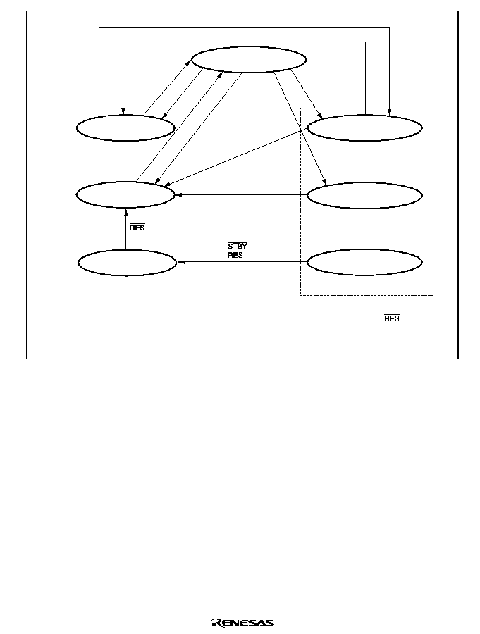
Rev. 2.0, 04/02, page 55 of 906
Exception
handling state
Bus-released state
Software standby
mode
Reset state
*1
Sleep mode
Power down state
*3
Program execution state
End of bus request
Bus request
= High
= High,
= Low
Reset state
Hardware standby
mode
*2
End of bus request
Bus request
Request for exception handling
Interrupt request
External interrupt request
SSBY = 0
SLEEP
instruction
SSBY = 1
SLEEP instruction
End of exception handling
Notes: 1. From any state except hardware standby mode, a transition to the reset state occurs whenever
goes low.
A transition can also be made to the reset state when the watchdog timer overflows.
2. In every state, when the STBY pin becomes low, the hardware standby mode is entered.
3. For details, refer to section 22, Power-Down Modes.
Figure 2.13 State Transitions
2.9
Usage Note
2.9.1
Usage Notes on Bit-wise Operation Instructions
The BSET, BCLR, BNOT, BST, and BIST instructions are used to read data in byte-wise, operate
the data in bit-wise, and write the result of the bit-wise operation in bit-wise again. Therefore,
special care is necessary to use these instructions for the registers and the ports that include write-
only bit.
The BCLR instruction can be used to clear the flags in the internal I/O registers to 0. In this time,
if it is obvious that the flag has been set to 1 in the interrupt handler, there is no need to read the
flag beforehand.

Rev. 2.0, 04/02, page 56 of 906

Rev. 2.0, 04/02, page 57 of 906
Section 3 MCU Operating Modes
3.1
Operating Mode Selection
The H8S/2678 Series has twelve operating modes (modes 1, 2, 4 to 7, and 10 to 15). All operating
modes are available for the flash memory version. Modes 1, 2, and 4 to 7 are available in the
masked ROM version. Modes 1 and 2 are available in the ROMless version.
The H8S/2678R Series has seven operating modes (modes 1 to 7). All operating modes are
available for the flash memory version. Modes 1 and 2 are available in the ROMless version.
These modes are determined by the mode pin (MD2 to MD0) setting.
Modes 1, 2, and 4 to 6 are externally expanded modes in which the CPU can access an external
memory and peripheral devices. In the externally expanded mode, each area can be switched to 8-
bit or 16-bit address space by the bus controller. If one of areas is set to 16-bit address space, the
bus mode is 16 bits. If all areas are set to 8-bit address space, the bus mode is 8 bits.
Mode 7 is a single-chip activation externally expanded mode in which the CPU can switch to
access an external memory and peripheral devices at the beginning of a program execution.
Modes 3, 10, and 11 are boot modes in which the flash memory can be accessed.
Modes 12 to 15 are user program modes in which the flash memory can be accessed.
For details, refer to section 19, Flash Memory.
Do not change the FWE and MD2 to MD0 pin settings during operation.

Rev. 2.0, 04/02, page 58 of 906
Table 3.1
MCU Operating Mode Selection
External Data
Bus
MCU
Operating
Mode
*
1
FWE
*
2
MD2
MD1
MD0
CPU
Operating
Mode
Description
On-Chip
ROM
Initial
Width
Max.
Value
1
0
0
0
1
Advanced
Expanded mode with
on-chip ROM disabled
Disabled
16 bits
16 bits
2
0
0
1
0
Advanced
Expanded mode with
on-chip ROM disabled
Disabled
8 bits
16 bits
3
--
0
1
1
Advanced
Boot mode
Enabled
--
16 bits
4
0
1
0
0
Advanced
Expanded mode with
on-chip ROM enabled
Enabled
8 bits
16 bits
5
0
1
0
1
Advanced
Expanded mode with
on-chip ROM enabled
Enabled
16 bits
16 bits
6
0
1
1
0
Advanced
Expanded mode with
on-chip ROM enabled
Enabled
8 bits
16 bits
7
0
1
1
1
Advanced
Single-chip mode
Enabled
--
16 bits
10
1
0
1
0
Advanced
Boot mode
Enabled
8 bits
16 bits
11
1
0
1
1
Advanced
Boot mode
Enabled
--
16 bits
12
1
1
0
0
Advanced
User program mode
Enabled
8 bits
16 bits
13
1
1
0
1
Advanced
User program mode
Enabled
16 bits
16 bits
14
1
1
1
0
Advanced
User program mode
Enabled
8 bits
16 bits
15
1
1
1
1
Advanced
User program mode
Enabled
--
16 bits
Notes: 1. Modes 1, 2, 4 to 7, and 10 to 15 are supported in the H8S/2678 Series.
Modes 1 to 7 are supported in the H8S/2678R Series.
2. The FWE pin setting is available only in the H8S/2678 Series. The FWE pin is not
available in the H8S/2678R Series.

Rev. 2.0, 04/02, page 59 of 906
3.2
Register Descriptions
The following registers are related to the operating mode.
∑
Mode control register (MDCR)
∑
System control register (SYSCR)
3.2.1
Mode Control Register (MDCR)
MDCR monitors the current operating mode of the H8S/2678 Series chip.
Bit
Bit Name
Initial Value
R/W
Descriptions
7 to
3
-
All 0
-
Reserved
These bits are always read as 0 and cannot be
modified.
2
1
0
MDS2
MDS1
MDS0
-
*
-
*
-
*
R
R
R
Mode Select 2 to 0
These bits indicate the input levels at pins MD2 to MD0
(the current operating mode). Bits MDS2 to MDS0
correspond to MD2 to MD0. MDS2 to MDS0 are read-
only bits and they cannot be written to. The mode pin
(MD2 to MD0) input levels are latched into these bits
when MDCR is read. These latches are canceled by a
reset.
Note: Determined by pins MD2 to MD0.
3.2.2
System Control Register (SYSCR)
SYSCR selects saturating or non-saturating calculation for the MAC instruction, controls CPU
access to the flash memory control registers (FLMCR1, FLMCR2, EBR1, and EBR2), sets
external bus mode, and enables or disables on-chip RAM.

Rev. 2.0, 04/02, page 60 of 906
Bit
Bit Name
Initial Value
R/W
Descriptions
7
6
-
-
1
1
R/W
R/W
Reserved
The initial value should not be modified.
5
MACS
0
R/W
MAC Saturation
Selects either saturating or non-saturating calculation
for the MAC instruction.
0: Non-saturating calculation for MAC instruction
1: Saturating calculation for MAC instruction
4
-
0
R/W
Reserved
The initial value should not be modified.
3
FLSHE
0
R/W
Flash Memory Control Register Enable
Controls CPU access to the flash memory control
registers (FLMCR1, FLMCR2, EBR1, and EBR2). If
this bit is set to 1, the flash memory control registers
can be read/written to. If this bit is cleared to 0, the
flash memory control registers are not selected. At this
time, the contents of the flash memory control registers
are maintained. This bit should be written to 0 other
than flash memory version.
0: Flash memory control registers are not selected for
area H'FFFFC8 to H'FFFFCB
1: Flash memory control registers are selected for area
H'FFFFC8 to H'FFFFCB
2
-
0
-
Reserved
This bit is always read as 0 and cannot be modified.
1
EXPE
-
R/W
External Bus Mode Enable
Sets external bus mode.
In modes 1, 2, and 4 to 6, this bit is fixed at 1 and
cannot be modified. In mode 3
*
and 7, this bit has an
initial value of 0, and can be read and written.
Writing of 0 to EXPE when its value is 1 should only be
carried out when an external bus cycle is not being
executed.
0: External bus disabled
1: External bus enabled
0
RAME
1
R/W
RAM Enable
Enables or disables the on-chip RAM. The RAME bit is
initialized when the reset status is released.
0: On-chip RAM is disabled
1: On-chip RAM is enabled
Note: Mode 3 is available only in the F-ZTAT version of H8S/2678R Series.

Rev. 2.0, 04/02, page 61 of 906
3.3
Operating Mode Descriptions
3.3.1
Mode 1
The CPU can access a 16-Mbyte address space in advanced mode. The on-chip ROM is disabled.
Ports A, B, and C function as an address bus, ports D and E function as a data bus, and parts of
ports F, G, and H carry bus control signals.
The initial bus mode after a reset is 16 bits, with 16-bit access to all areas. However, if 8-bit access
is designated for all areas by the bus controller, the bus mode switches to 8 bits.
3.3.2
Mode 2
The CPU can access a 16-Mbyte address space in advanced mode. The on-chip ROM is disabled.
Ports A, B, and C function as an address bus, ports D and E function as a data bus, and parts of
ports F, G, and H carry bus control signals.
The initial bus mode after a reset is 8 bits, with 8-bit access to all areas. However, if 16-bit access
is designated for all areas by the bus controller, the bus mode switches to 16 bits and port E
functions as a data bus.
3.3.3
Mode 3
This mode is a boot mode of the flash memory. This mode is the same as mode 7, except for
accessing to the flash memory. Mode 3 is available only in the flash memory version of the
H8S/2678R Series.
3.3.4
Mode 4
The CPU can access a 16-Mbyte address space in advanced mode. The on-chip ROM is enabled.
The program in the on-chip ROM connected to the first half of area 0 is executed.
Ports A, B, and C function as input ports immediately after a reset, but can be set to function as an
address bus. For details, see section 10, I/O Ports. Ports D and E function as a data bus, and parts
of ports F, G, and H carry bus control signals.
The initial bus mode after a reset is 8 bits, with 8-bit access to all areas. However, if 16-bit access
is designated for any area by the bus controller, the bus mode switches to 16 bits and port E
functions as a data bus. In the flash memory version, user program mode is entered by setting 1 to
the SWE bit of FLMCR1.

Rev. 2.0, 04/02, page 62 of 906
3.3.5
Mode 5
The CPU can access a 16-Mbyte address space in advanced mode. The on-chip ROM is enabled.
The program in an external ROM connected to the first half of area 0 is executed.
Ports A, B, and C function as an address bus, ports D and E function as a data bus, and parts of
ports F, G and H carry bus control signals.
The initial bus mode after a reset is 16 bits, with 16-bit access to all areas. However, if 8-bit access
is designated for any area by the bus controller, the bus mode switches to 8 bits.
In the flash memory version, user program mode is entered by setting 1 to the SWE bit of
FLMCR1.
3.3.6
Mode 6
The CPU can access a 16-Mbyte address space in advanced mode. The on-chip ROM is enabled.
The program in an external ROM connected to the first half of area 0 is executed.
Ports A, B, and C function as an address bus, ports D and E function as a data bus, and parts of
ports F, G, and H carry bus control signals.
The initial bus mode after a reset is 8 bits, with 8-bit access to all areas. However, if 16-bit access
is designated for any area by the bus controller, the bus mode switches to 16 bits and port E
functions as a data bus.
In the flash memory version, user program mode is entered by setting 1 to the SWE bit of
FLMCR1.
3.3.7
Mode 7
The CPU can access a 16-Mbyte address space in advanced mode. The on-chip ROM is enabled,
and the chip starts up in single-chip mode. External addresses cannot be used in single-chip mode.
The initial mode after a reset is single-chip mode, with all I/O ports available for use as
input/output ports. However, the mode can be switched to externally expanded mode by setting 1
to the EXPE bit of SYSCR and then the external address space is enabled. When externally
expanded mode is selected, all areas are initially designated as 16-bit access space. The function of
pins in ports A to H is the same as in externally expanded mode with on-chip ROM enabled.
In the flash memory version, user program mode is entered by setting 1 to the SWE bit of
FLMCR1.

Rev. 2.0, 04/02, page 63 of 906
3.3.8
Mode 10
This is flash memory boot mode. This mode is the same as mode 4, except for accessing to the
flash memory. Mode 10 is available only in the flash memory version of the H8S/2678 Series.
3.3.9
Mode 11
This is flash memory boot mode. This mode is the same as mode 7, except for accessing to the
flash memory. Mode 11 is available only in the flash memory version of the H8S/2678 Series.
3.3.10
Mode 12
This is flash memory user program mode. This mode is the same as mode 4, except for accessing
to the flash memory. Mode 12 is available only in the flash memory version of the H8S/2678
Series.
3.3.11
Mode 13
This is flash memory user program mode. This mode is the same as mode 5, except for accessing
to the flash memory. Mode 13 is available only in the flash memory version of the H8S/2678
Series.
3.3.12
Mode 14
This is flash memory user program mode. This mode is the same as mode 6, except for accessing
to the flash memory. Mode 14 is available only in the flash memory version of the H8S/2678
Series.
3.3.13
Mode 15
This is flash memory user program mode. This mode is the same as mode 7, except for accessing
to the flash memory. Mode 15 is available only in the flash memory version of the H8S/2678
Series.
3.3.14
Pin Functions
The pin functions of ports A to H are switched according to operating mode. Table 3.2 shows the
pin functions in each operating mode.

Rev. 2.0, 04/02, page 64 of 906
Table 3.2
Pin Functions in Each Operating Mode
Port
Mode
1
Mode
2
Mode
3
Mode
4
Mode
5
Mode
6
Mode
7
Mode
10
Mode
11
Mode
12
Mode
13
Mode
14
Mode
15
PA7 to
PA5
P
*
/A
P
*
/A
P
*
/A
P
*
/A
P
*
/A
P
*
/A
Port A
PA4 to
PA0
A
A
P
*
/A
P
*
/A
A
A
P
*
/A
P
*
/A
P
*
/A
A
P
*
/A
A
P
*
/A
Port B
A
A
P
*
/A
P
*
/A
A
A
P
*
/A
P
*
/A
P
*
/A
P
*
/A
A
A
P
*
/A
Port C
A
A
P
*
/A
P
*
/A
A
A
P
*
/A
P
*
/A
P
*
/A
P
*
/A
A
A
P
*
/A
Port D
D
D
P
*
/D
P
*
/D
D
D
P
*
/D
D
P
*
/D
D
D
D
P
*
/D
Port E
P/D
*
P
*
/D
P
*
/D
P
*
/D
P/D
*
P
*
/D
P
*
/D
P
*
/D
P
*
/D
P
*
/D
P/D
*
P
*
/D
P
*
/D
PF7,
PF6
P/C
*
P
*
/C
P/C
*
P/C
*
P/C
*
P
*
/C
P/C
*
P/C
*
P/C
*
PF5,
PF4
C
C
C
C
C
C
C
C
C
PF3
P/C
*
P/C
*
P/C
*
P/C
*
P/C
*
P/C
*
P/C
*
P/C
*
P/C
*
Port F
PF2 to
PF0
P
*
/C
P
*
/C
P
*
/C
P
*
/C
P
*
/C
P
*
/C
P
*
/C
P
*
/C
P
*
/C
P
*
/C
P
*
/C
P
*
/C
P
*
/C
PG6 to
PG1
P
*
/C
P
*
/C
P
*
/C
P
*
/C
P
*
/C
P
*
/C
P
*
/C
P
*
/C
P
*
/C
Port G
PG0
P/C
*
P/C
*
P
*
/C
P
*
/C
P/C
*
P/C
*
P
*
/C
P/C
*
P
*
/C
P
*
/C
P/C
*
P/C
*
P
*
/C
Port H
P
*
/C
P
*
/C
P
*
/C
P
*
/C
P
*
/C
P
*
/C
P
*
/C
P
*
/C
P
*
/C
P
*
/C
P
*
/C
P
*
/C
P
*
/C
Legend: P: I/O port
A: Address bus output
D: Data bus input/output
C: Control signals, clock input/output
Note: After reset
Rev. 2.0, 04/02, page 65 of 906
3.4
Memory Map in Each Operating Mode
Figures 3.1 to 3.6 show memory maps for each product.
H'000000
H'FFA000
H'FFC000
H'000000
H'FFA000
H'FFC000
H'FFFC00
External
address space
On-chip RAM/external
address space
*
External address space
Internal I/O registers
External address space
Internal I/O registers
On-chip ROM
On-chip RAM/external
address space
*
External address space
Internal I/O registers
External address space
Internal I/O registers
H'FFFFFF
H'FFFC00
H'FFFF00
H'FFFF20
H'FFFFFF
H'FFFF00
H'FFFF20
H'040000
External
address space
RAM : 8 kbytes
Modes 1 and 2
(expanded modes
with on-chip ROM disabled)
ROM : 256 kbytes
RAM : 8 kbytes
Mode 4
(expanded mode
with on-chip ROM enabled)
Note:
*
This area is specified as an external address area by clearing the RAME bit of SYSCR to 0.
Figure 3.1 H8S/2676 Memory Map (1)
Rev. 2.0, 04/02, page 66 of 906
H'000000
H'FFA000
H'FFC000
H'000000
H'FFA000
H'FFC000
H'FFFC00
External
address space
On-chip RAM/external
address space
*
1
External
address space
External address space
Internal I/O registers
External address space
Internal I/O registers
On-chip ROM
On-chip RAM/external
address space
*
3
External address
space/reserved area
*
2
External address
space/reserved area
*
2
Internal I/O registers
Internal I/O registers
H'FFFFFF
H'FFFC00
H'FFFF00
H'FFFF20
H'FFFFFF
H'FFFF00
H'FFFF20
H'040000
H'100000
H'140000
External address
space/reserved area
*
2
On-chip ROM
ROM : 256 kbytes
RAM : 8 kbytes
Modes 5 and 6
(external ROM activation
expanded modes
with on-chip ROM enabled)
ROM : 256 kbytes
RAM : 8 kbytes
Mode 7
(single-chip activation
expanded mode
with on-chip ROM enabled)
Notes: 1. This area is specified as an external address area by clearing the RAME bit of SYSCR to 0.
2. When EXPE = 1, external address space; when EXPE = 0, reserved area.
3. When EXPE = 1, external address space when RAME = 0, on-chip RAM when RAME = 1.
When EXPE = 0, on-chip RAM area.
Figure 3.1 H8S/2676 Memory Map (2)
Rev. 2.0, 04/02, page 67 of 906
H'000000
H'FFA000
H'FFC000
H'000000
H'FFA000
H'FFC000
H'FFFC00
On-chip RAM
*
2
External
address space
External address space
Internal I/O registers
External address space
Internal I/O registers
On-chip ROM
On-chip RAM
*
2
External address
space/reserved area
*
1
External address
space/reserved area
*
1
Internal I/O registers
Internal I/O registers
H'FFFFFF
H'FFFC00
H'FFFF00
H'FFFF20
H'FFFFFF
H'FFFF00
H'FFFF20
H'040000
H'040000
External address
space/reserved area
*
1
On-chip ROM
ROM : 256 kbytes
RAM : 8 kbytes
Mode 10 Boot mode
(expanded mode
with on-chip ROM enabled)
ROM : 256 kbytes
RAM : 8 kbytes
Mode 11 Boot mode
(single-chip activation expanded mode
with on-chip ROM enabled)
Notes: 1. When EXPE = 1, external address space; when EXPE = 0, reserved area.
2. On-chip RAM is used for flash memory programming. Do not clear the RAME bit in SYSCR to 0.
Figure 3.1 H8S/2676 Memory Map (3)
Rev. 2.0, 04/02, page 68 of 906
H'000000
H'FFA000
H'FFC000
H'000000
H'FFA000
H'FFC000
H'FFFC00
On-chip RAM
*
2
External
address space
External address space
Internal I/O registers
External address space
Internal I/O registers
On-chip ROM
On-chip RAM
*
2
External address
space/reserved area
*
1
External address
space/reserved area
*
1
Internal I/O registers
Internal I/O registers
H'FFFFFF
H'FFFC00
H'FFFF00
H'FFFF20
H'FFFFFF
H'FFFF00
H'FFFF20
H'040000
H'040000
External address
space/reserved area
*
1
On-chip ROM
ROM : 256 kbytes
RAM : 8k bytes
Mode 12 User program mode
(expanded mode
with on-chip ROM enabled)
ROM : 256 kbytes
RAM : 8 kbytes
Mode 15 User program mode
(single-chip activation
expanded mode
with on-chip ROM enabled)
Notes: 1. When EXPE = 1, external address space; when EXPE = 0, reserved area.
2. On-chip RAM is used for flash memory programming. Do not clear the RAME bit in SYSCR to 0.
H'000000
H'FFA000
H'FFC000
External
address space
On-chip RAM
*
2
External
address space
External address space
Internal I/O registers
External address space
Internal I/O registers
H'FFFFFF
H'FFFC00
H'FFFF00
H'FFFF20
H'100000
H'140000
On-chip ROM
ROM : 256 kbytes
RAM : 8 kbytes
Modes 13 and 14 User program mode
(external ROM activation
expanded modes
with on-chip ROM enabled)
Figure 3.1 H8S/2676 Memory Map (4)

Rev. 2.0, 04/02, page 69 of 906
H'000000
H'FFA000
H'FFC000
H'000000
H'FFA000
H'FFC000
H'FFFC00
External
address space
On-chip RAM/external
address space
*
External address space
Internal I/O registers
External address space
Internal I/O registers
On-chip ROM
On-chip RAM/external
address space
*
External address space
Internal I/O registers
External address space
Internal I/O registers
H'FFFFFF
H'FFFC00
H'FFFF00
H'FFFF20
H'FFFFFF
H'FFFF00
H'FFFF20
H'020000
External
address space
RAM : 8 k bytes
Modes 1 and 2
(expanded modes
with on-chip ROM disabled)
ROM : 128 kbytes
RAM : 8k bytes
Mode 4
(expanded mode
with on-chip ROM enabled)
Note:
*
This area is specified as an external address area by clearing the RAME bit of SYSCR to 0.
Figure 3.2 H8S/2675 Memory Map (1)
Rev. 2.0, 04/02, page 70 of 906
H'000000
H'FFA000
H'FFC000
H'000000
H'FFA000
H'FFC000
H'FFFC00
External
address space
On-chip RAM/external
address space
*
1
External
address space
External address space
Internal I/O registers
External address space
Internal I/O registers
On-chip ROM
On-chip RAM/external
address space
*
3
External address
space/reserved area
*
2
External address
space/reserved area
*
2
Internal I/O registers
Internal I/O registers
H'FFFFFF
H'FFFC00
H'FFFF00
H'FFFF20
H'FFFFFF
H'FFFF00
H'FFFF20
H'020000
H'100000
H'120000
External address
space/reserved area
*
2
On-chip ROM
ROM : 128 kbytes
RAM : 8 kbytes
Modes 5 and 6
(external ROM activation
expanded modes
with on-chip ROM enabled)
ROM : 128 kbytes
RAM : 8 kbytes
Mode 7
(single-chip activation
expanded mode
with on-chip ROM enabled)
Notes: 1. This area is specified as an external address area by clearing the RAME bit of SYSCR to 0.
2. When EXPE = 1, external address space; when EXPE = 0, reserved area.
3. When EXPE = 1, external address space when RAME = 0, on-chip RAM when RAME = 1.
When EXPE = 0, on-chip RAM area.
Figure 3.2 H8S/2675 Memory Map (2)
Rev. 2.0, 04/02, page 71 of 906
H'000000
H'FFA000
H'FFC000
H'000000
H'FFA000
H'FFC000
H'FFFC00
External
address space
On-chip RAM/external
address space
*
External address space
Internal I/O registers
External address space
Internal I/O registers
On-chip ROM
On-chip RAM/external
address space
*
External address space
Internal I/O registers
External address space
Internal I/O registers
H'FFFFFF
H'FFFC00
H'FFFF00
H'FFFF20
H'FFFFFF
H'FFFF00
H'FFFF20
H'010000
External
address space
RAM : 8 kbytes
Modes 1 and 2
(expanded modes
with on-chip ROM disabled)
ROM : 64 kbytes
RAM : 8 kbytes
Mode 4
(expanded mode
with on-chip ROM enabled)
Note:
*
This area is specified as an external address area by clearing the RAME bit of SYSCR to 0.
Figure 3.3 H8S/2673 Memory Map (1)
Rev. 2.0, 04/02, page 72 of 906
H'000000
H'FFA000
H'FFC000
H'000000
H'FFA000
H'FFC000
H'FFFC00
External
address space
On-chip RAM/external
address space
*
1
External
address space
External address space
Internal I/O registers
External address space
Internal I/O registers
On-chip ROM
On-chip RAM/external
address space
*
3
External address
space/reserved area
*
2
External address
space/reserved area
*
2
Internal I/O registers
Internal I/O registers
H'FFFFFF
H'FFFC00
H'FFFF00
H'FFFF20
H'FFFFFF
H'FFFF00
H'FFFF20
H'010000
H'100000
H'110000
External address
space/reserved area
*
2
On-chip ROM
ROM : 64 kbytes
RAM : 8 kbytes
Modes 5 and 6
(external ROM activation
expanded modes
with on-chip ROM enabled)
ROM : 64 kbytes
RAM : 8 kbytes
Mode 7
(single-chip activation
expanded mode
with on-chip ROM enabled)
Notes: 1. This area is specified as an external address area by clearing the RAME bit of SYSCR to 0.
2. When EXPE = 1, external address space; when EXPE = 0, reserved area.
3. When EXPE = 1, external address space when RAME = 0, on-chip RAM when RAME = 1.
When EXPE = 0, on-chip RAM area.
Figure 3.3 H8S/2673 Memory Map (2)

Rev. 2.0, 04/02, page 73 of 906
H'000000
H'FFA000
H'FFC000
External
address space
On-chip RAM/external
address space
*
External address space
Internal I/O registers
External address space
Internal I/O registers
H'FFFFFF
H'FFFC00
H'FFFF00
H'FFFF20
RAM : 8 kbytes
Modes 1 and 2
(expanded modes
with on-chip ROM disabled)
Note:
*
This area is specified as an external address area by clearing the RAME bit of SYSCR to 0.
Figure 3.4 H8S/2670 Memory Map
Rev. 2.0, 04/02, page 74 of 906
H'000000
H'FF4000
H'FFC000
External
address space
On-chip RAM/external
address space
*
External address space
Internal I/O registers
External address space
Internal I/O registers
H'FFFFFF
H'FFFC00
H'FFFF00
H'FFFF20
RAM : 32 kbytes
Modes 1 and 2
(expanded modes
with on-chip ROM disabled)
Note:
*
This area is specified as an external address area by clearing the RAME bit of SYSCR to 0.
Figure 3.5 H8S/2674R Memory Map

Rev. 2.0, 04/02, page 75 of 906
Section 4 Exception Handling
4.1
Exception Handling Types and Priority
As table 4.1 indicates, exception handling may be caused by a reset, trace, interrupt, or trap
instruction. Exception handling is prioritized as shown in table 4.1. If two or more exceptions
occur simultaneously, they are accepted and processed in order of priority. Exception sources, the
stack structure, and operation of the CPU vary depending on the interrupt control mode. For
details on the interrupt control mode, refer to section 5, Interrupt Controller.
Table 4.1
Exception Types and Priority
Priority
Exception Type
Start of Exception Handling
High
Reset
Starts immediately after a low-to-high transition at the
#$
pin, or when the watchdog timer overflows. The CPU enters
the reset state when the
#$
pin is low.
Trace
*
1
Starts when execution of the current instruction or exception
handling ends, if the trace (T) bit in the EXR is set to 1.
Direct transition
*
2
Starts when the direct transition occurs by execution of the
SLEEP instruction.
Interrupt
Starts when execution of the current instruction or exception
handling ends, if an interrupt request has been issued.
*
3
Low
Trap instruction
*
4
Started by execution of a trap instruction (TRAPA)
Notes: 1. Traces are enabled only in interrupt control mode 2. Trace exception handling is not
executed after execution of an RTE instruction.
2. Not available in this LSI.
3. Interrupt detection is not performed on completion of ANDC, ORC, XORC, or LDC
instruction execution, or on completion of reset exception handling.
4. Trap instruction exception handling requests are accepted at all times in program
execution state.
4.2
Exception Sources and Exception Vector Table
Different vector addresses are assigned to different exception sources. Table 4.2 lists the exception
sources and their vector addresses. Since the usable modes differ depending on the product, for
details on each product, refer to section 3, MCU Operating Modes.

Rev. 2.0, 04/02, page 76 of 906
Table 4.2
Exception Handling Vector Table
Vector Address
*
1
Exception Source
Vector Number
Normal Mode
*
2
Advanced Mode
Power-on reset
0
H'0000 to H'0001
H'0000 to H'0003
Manual reset
*
2
1
H'0002 to H'0003
H'0004 to H'0007
Reserved for system use
2
H'0004 to H'0005
H'0008 to H'000B
3
H'0006 to H'0007
H'000C to H'000F
4
H'0008 to H'0019
H'0010 to H'0013
Trace
5
H'000A to H'000B
H'0014 to H'0017
Interrupt (direct transition)
*
2
6
H'000C to H'000D
H'0018 to H'001B
Interrupt (NMI)
7
H'000E to H'000F
H'001C to H'001F
Trap instruction (#0)
8
H'0010 to H'0011
H'0020 to H'0023
(#1)
9
H'0012 to H'0013
H'0024 to H'0027
(#2)
10
H'0014 to H'0015
H'0028 to H'002B
(#3)
11
H'0016 to H'0017
H'002C to H'002F
Reserved for system use
12
H'0018 to H'0019
H'0030 to H'0033
13
H'001A to H'001B
H'0034 to H'0037
14
H'001C to H'001D
H'0038 to H'003B
15
H'001E to H'001F
H'003C to H'003F
External interrupt
IRQ0
16
H'0020 to H'0021
H'0040 to H'0043
IRQ1
17
H'0022 to H'0023
H'0044 to H'0047
IRQ2
18
H'0024 to H'0025
H'0048 to H'004B
IRQ3
19
H'0026 to H'0027
H'004C to H'004F
IRQ4
20
H'0028 to H'0029
H'0050 to H'0053
IRQ5
21
H'002A to H'002B
H'0054 to H'0057
IRQ6
22
H'002C to H'002D
H'0058 to H'005B
IRQ7
23
H'002E to H'002F
H'005C to H'005F
IRQ8
24
H'0030 to H'0031
H'0060 to H'0063
IRQ9
25
H'0032 to H'0033
H'0064 to H'0067
IRQ10
26
H'0034 to H'0035
H'0068 to H'006B
IRQ11
27
H'0036 to H'0037
H'006C to H'006F
IRQ12
28
H'0038 to H'0039
H'0070 to H'0073
IRQ13
29
H'003A to H'003B
H'0074 to H'0077
IRQ14
30
H'003C to H'003D
H'0078 to H'007B
IRQ15
31
H'003E to H'003F
H'007C to H'007F

Rev. 2.0, 04/02, page 77 of 906
Vector Address
*
1
Exception Source
Vector Number
Normal Mode
*
2
Advanced Mode
Internal interrupt
*
3
32
99
H'0040 to H'0041
H'00C6 to H'00C7
H'0080 to H'0083
H'018C to H'018F
Notes: 1. Lower 16 bits of the address.
2. Not available in this LSI.
3. For details of internal interrupt vectors, see section 5.5, Interrupt Exception Handling
Vector Table.
4.3
Reset
A reset has the highest exception priority. When the
#$ pin goes low, all processing halts and
this LSI enters the reset. To ensure that this LSI is reset, hold the
#$ pin low for at least 20 ms at
power-up. To reset the chip during operation, hold the
#$ pin low for at least 20 states. A reset
initializes the internal state of the CPU and the registers of on-chip peripheral modules.
The chip can also be reset by overflow of the watchdog timer. For details see section 14,
Watchdog Timer.
The interrupt control mode is 0 immediately after reset.
4.3.1
Reset exception handling
When the
#$ pin goes high after being held low for the necessary time, this LSI starts reset
exception handling as follows:
1. The internal state of the CPU and the registers of the on-chip peripheral modules are
initialized, the T bit is cleared to 0 in EXR, and the I bit is set to 1 in EXR and CCR.
2. The reset exception handling vector address is read and transferred to the PC, and program
execution starts from the address indicated by the PC.
Figures 4.1 and 4.2 show examples of the reset sequence.
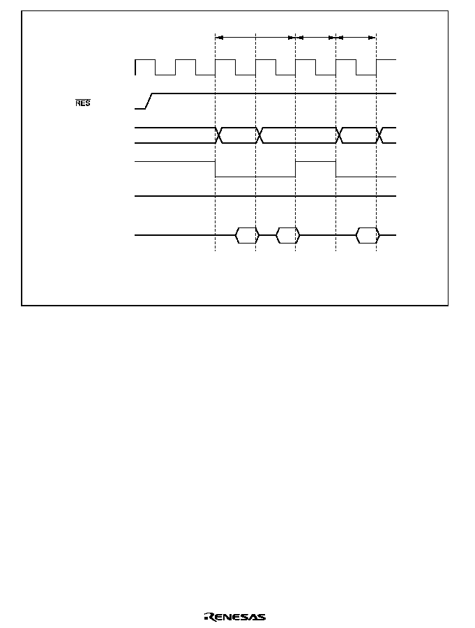
Rev. 2.0, 04/02, page 78 of 906
High
Vector fetch
Internal
processing
Prefetch of first
program instruction
(1)(3) Reset exception handling vector address (when reset, (1)=H'000000, (3)=H'000002)
(2)(4) Start address (contents of reset exception handling vector address)
(5) Start address ((5)=(2)(4))
(6) First program instruction
Internal
address bus
Internal read
signal
Internal write
signal
Internal data
bus
(1)
(2)
(4)
(6)
(3)
(5)
Figure 4.1 Reset Sequence (Advanced Mode with On-chip ROM Enabled)
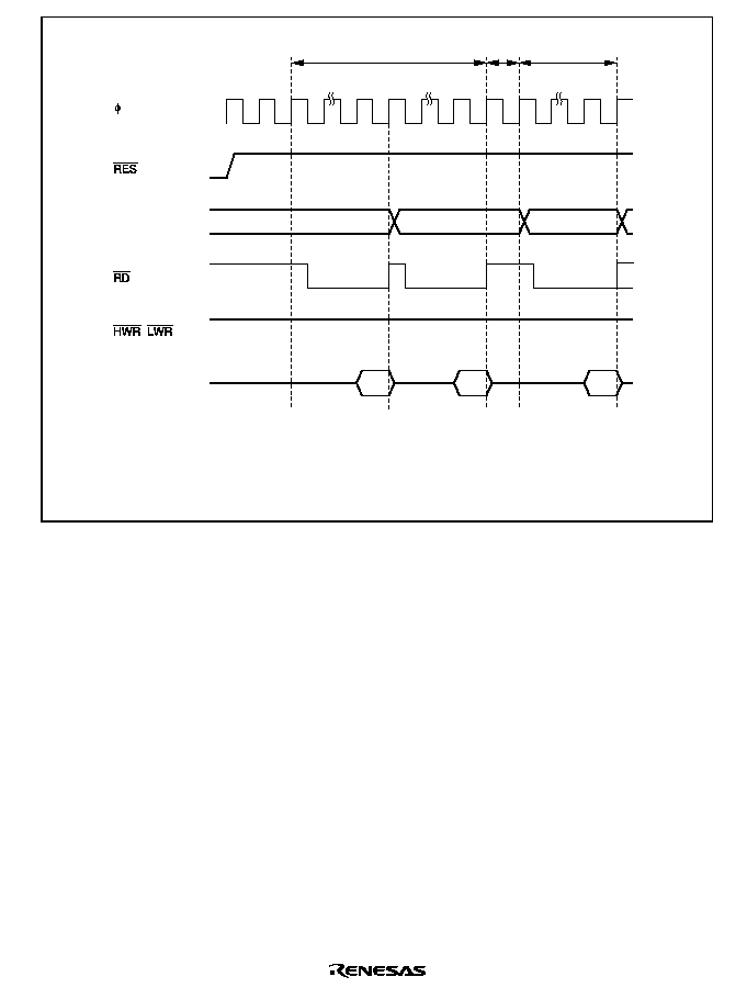
Rev. 2.0, 04/02, page 79 of 906
,
D15 to D0
High
*
*
*
Address bus
Vector fetch
Internal
processing
Prefetch of first
program instruction
(1)
(2)
(4)
(6)
(3)
(5)
(1)(3) Reset exception handling vector address (when reset, (1)=H'000000, (3)=H'000002)
(2)(4) Start address (contents of reset exception handling vector address)
(5) Start address ((5)=(2)(4))
(6) First program instruction
Note:
*
Seven program wait states are inserted.
Figure 4.2 Reset Sequence (Advanced Mode with On-chip ROM Disabled)
4.3.2
Interrupts after Reset
If an interrupt is accepted after a reset but before the stack pointer (SP) is initialized, the PC and
CCR will not be saved correctly, leading to a program crash. To prevent this, all interrupt requests,
including NMI, are disabled immediately after a reset. Since the first instruction of a program is
always executed immediately after the reset state ends, make sure that this instruction initializes
the stack pointer (example: MOV.L #xx: 32, SP).
4.3.3
On-Chip Peripheral Functions after Reset Release
After reset release, MSTPCR is initialized to H'0FFF and all modules except the DMAC,
EXDMAC and the DTC enter module stop mode.
Consequently, on-chip peripheral module registers cannot be read or written to. Register reading
and writing is enabled when module stop mode is exited.

Rev. 2.0, 04/02, page 80 of 906
4.4
Traces
Traces are enabled in interrupt control mode 2. Trace mode is not activated in interrupt control
mode 0, irrespective of the state of the T bit. For details on interrupt control modes, see section 5,
Interrupt Controller.
If the T bit in EXR is set to 1, trace mode is activated. In trace mode, a trace exception occurs on
completion of each instruction. Trace mode is not affected by interrupt masking. Table 4.3 shows
the state of CCR and EXR after execution of trace exception handling. Trace mode is canceled by
clearing the T bit in EXR to 0. The T bit saved on the stack retains its value of 1, and when control
is returned from the trace exception handling routine by the RTE instruction, trace mode resumes.
Trace exception handling is not carried out after execution of the RTE instruction.
Interrupts are accepted even within the trace exception handling routine.
Table 4.3
Status of CCR and EXR after Trace Exception Handling
CCR
EXR
Interrupt Control Mode
I
UI
I2 to I0
T
0
Trace exception handling cannot be used.
2
1
--
--
0
Legend:
1:
Set to 1
0: Cleared to 0
--: Retains value prior to execution.
4.5
Interrupts
Interrupts are controlled by the interrupt controller. The interrupt controller has two interrupt
control modes and can assign interrupts other than NMI to eight priority/mask levels to enable
multiplexed interrupt control. The source to start interrupt exception handling and the vector
address differ depending on the product. For details, refer to section 5, Interrupt Controller.
The interrupt exception handling is as follows:
1. The values in the program counter (PC), condition code register (CCR), and extended register
(EXR) are saved in the stack.
2. The interrupt mask bit is updated and the T bit is cleared to 0.
3. A vector address corresponding to the interrupt source is generated, the start address is loaded
from the vector table to the PC, and program execution starts from that address.

Rev. 2.0, 04/02, page 81 of 906
4.6
Trap Instruction
Trap instruction exception handling starts when a TRAPA instruction is executed. Trap instruction
exception handling can be executed at all times in the program execution state.
The trap instruction exception handling is as follows:
1. The values in the program counter (PC), condition code register (CCR), and extended register
(EXR) are saved in the stack.
2. The interrupt mask bit is updated and the T bit is cleared to 0.
3. A vector address corresponding to the interrupt source is generated, the start address is loaded
from the vector table to the PC, and program execution starts from that address.
The TRAPA instruction fetches a start address from a vector table entry corresponding to a vector
number from 0 to 3, as specified in the instruction code.
Table 4.4 shows the status of CCR and EXR after execution of trap instruction exception handling.
Table 4.4
Status of CCR and EXR after Trap Instruction Exception Handling
CCR
EXR
Interrupt Control Mode
I
UI
I2 to I0
T
0
1
--
--
--
2
1
--
--
0
Legend:
1:
Set to 1
0:
Cleared to 0
--: Retains value prior to execution.
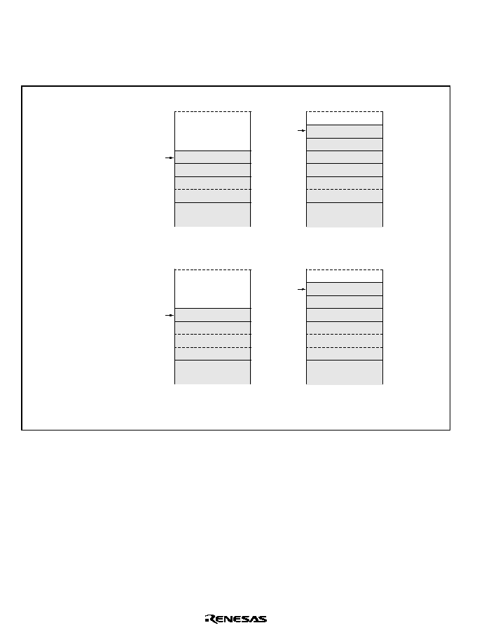
Rev. 2.0, 04/02, page 82 of 906
4.7
Stack Status after Exception Handling
Figure 4.3 shows the stack after completion of trap instruction exception handling and interrupt
exception handling.
CCR
CCR
*
1
PC (16 bits)
SP
EXR
Reserved
*
1
CCR
CCR
*
1
PC (16 bits)
SP
CCR
PC (24 bits)
SP
EXR
Reserved
*
1
CCR
PC (24 bits)
SP
(a) Normal Modes
*
2
(b) Advanced Modes
Interrupt control mode 0
Interrupt control mode 2
Interrupt control mode 0
Interrupt control mode 2
Note: 1.
2.
Ignored on return.
Normal modes are not available in this LSI.
Figure 4.3 Stack Status after Exception Handling
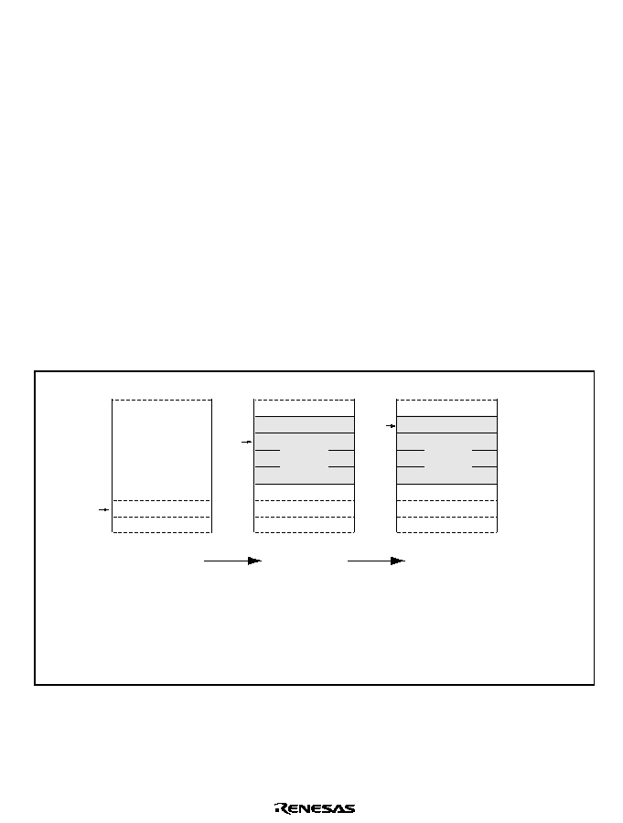
Rev. 2.0, 04/02, page 83 of 906
4.8
Usage Note
When accessing word data or longword data, this LSI assumes that the lowest address bit is 0. The
stack should always be accessed by word transfer instruction or longword transfer instruction, and
the value of the stack pointer (SP, ER7) should always be kept even. Use the following
instructions to save registers:
PUSH.W Rn (or MOV.W Rn, @-SP)
PUSH.L ERn (or MOV.L ERn, @-SP)
Use the following instructions to restore registers:
POP.W Rn (or MOV.W @SP+, Rn)
POP.L ERn (or MOV.L @SP+, ERn)
Setting SP to an odd value may lead to a malfunction. Figure 4.4 shows an example of operation
when the SP value is odd.
SP
CCR :
PC :
R1L :
SP :
Condition code register
Program counter
General register R1L
Stack pointer
CCR
SP
SP
R1L
H'FFFEFA
H'FFFEFB
H'FFFEFC
H'FFFEFD
H'FFFEFE
H'FFFEFF
PC
PC
TRAP instruction executed
SP set to H'FFFEFF
Data saved above SP
MOV.B R1L, @-ER7
Contents of CCR lost
Address
Legend
Note: This diagram illustrates an example in which the interrupt control mode is 0, in advanced mode.
Figure 4.4 Operation when SP Value Is Odd

Rev. 2.0, 04/02, page 84 of 906

Rev. 2.0, 04/02, page 85 of 906
Section 5 Interrupt Controller
5.1
Features
∑
Two interrupt control modes
Any of two interrupt control modes can be set by means of the INTM1 and INTM0 bits in the
interrupt control register (INTCR).
∑
Priorities settable with IPR
An interrupt priority register (IPR) is provided for setting interrupt priorities. Eight priority
levels can be set for each module for all interrupts except NMI. NMI is assigned the highest
priority level of 8, and can be accepted at all times.
∑
Independent vector addresses
All interrupt sources are assigned independent vector addresses, making it unnecessary for the
source to be identified in the interrupt handling routine.
∑
Seventeen external interrupts
NMI is the highest-priority interrupt, and is accepted at all times. Rising edge or falling edge
can be selected for NMI. Falling edge, rising edge, or both edge detection, or level sensing, can
be selected for
,54 to ,54.
∑
DTC and DMAC control
DTC and DMAC activations are performed by means of interrupts.
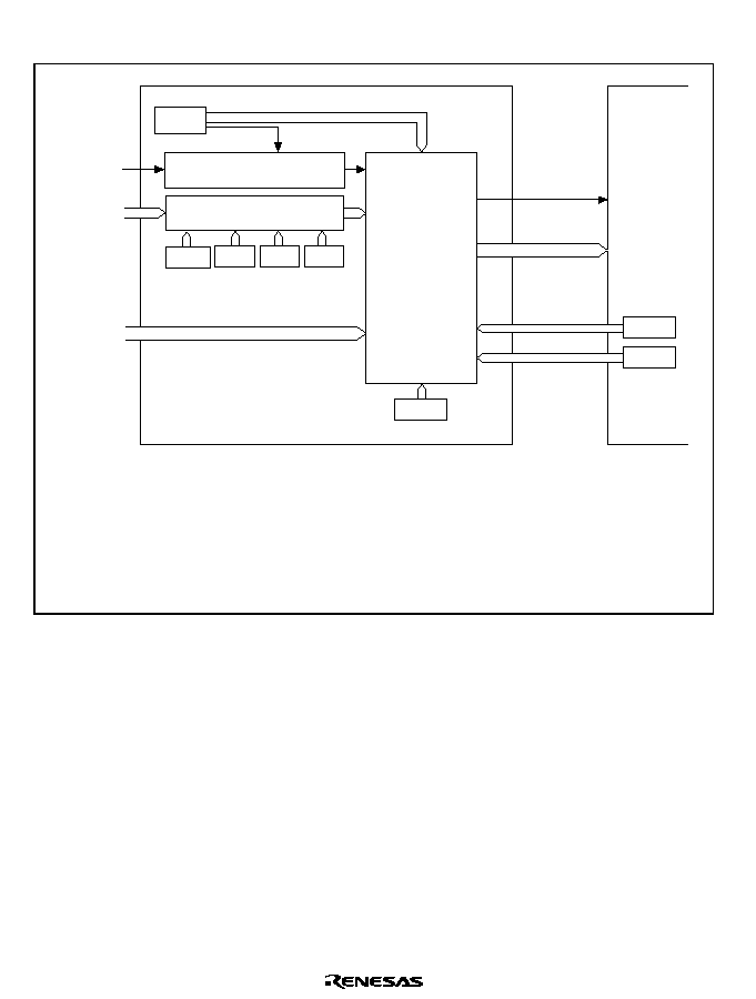
Rev. 2.0, 04/02, page 86 of 906
A block diagram of the interrupt controller is shown in figure 5.1.
INTCR
NMI input
IRQ input
Internal
interrupt
sources
SWDTEND
to TEI
INTM1 INTM0
NMIEG
NMI input unit
IRQ input unit
ISR
ISCR
ITSR
IER
IPR
Interrupt controller
Priority
determination
Interrupt
request
Vector
number
I
I2 to I0
CCR
EXR
CPU
Legend
ISCR:
IRQ sense control register
IER:
IRQ enable register
ISR:
IRQ status register
IPR:
Interrupt priority register
INTCR: Interrupt control register
ITSR:
IRQ pin select register
SSIER: Software standby release IRQ enable register
SSIER
Figure 5.1 Block Diagram of Interrupt Controller
5.2
Input/Output Pins
Table 5.1 shows the pin configuration of the interrupt controller.

Rev. 2.0, 04/02, page 87 of 906
Table 5.1
Pin Configuration
Name
I/O
Function
NMI
Input
Nonmaskable external interrupt
Rising or falling edge can be selected.
,54
to
,54
Input
Maskable external interrupts
Rising, falling, or both edges, or level sensing, can be
selected.
5.3
Register Descriptions
The interrupt controller has the following registers.
∑
Interrupt control register (INTCR)
∑
IRQ sense control register H (ISCRH)
∑
IRQ sense control register L (ISCRL)
∑
IRQ enable register (IER)
∑
IRQ status register (ISR)
∑
IRQ pin select register (ITSR)
∑
Software standby release IRQ enable register (SSIER)
∑
Interrupt priority register A (IPRA)
∑
Interrupt priority register B (IPRB)
∑
Interrupt priority register C (IPRC)
∑
Interrupt priority register D (IPRD)
∑
Interrupt priority register E (IPRE)
∑
Interrupt priority register F (IPRF)
∑
Interrupt priority register G (IPRG)
∑
Interrupt priority register H (IPRH)
∑
Interrupt priority register I (IPRI)
∑
Interrupt priority register J (IPRJ)
∑
Interrupt priority register K (IPRK)
5.3.1
Interrupt Control Register (INTCR)
INTCR selects the interrupt control mode, and the detected edge for NMI.

Rev. 2.0, 04/02, page 88 of 906
Bit
Bit Name
Initial Value
R/W
Description
7
6
-
-
0
0
R/W
R/W
Reserved
These bits can be read from or written to.
However, the write value should always be 0.
5
4
INTM1
INTM0
0
0
R/W
R/W
Interrupt Control Select Mode 1 and 0
These bits select either of two interrupt control
modes for the interrupt controller.
00: Interrupt control mode 0
Interrupts are controlled by I bit.
01: Setting prohibited.
10: Interrupt control mode 2
Interrupts are controlled by bits I2 to I0, and
IPR.
11: Setting prohibited.
3
NMIEG
0
R/W
NMI Edge Select
Selects the input edge for the NMI pin.
0: Interrupt request generated at falling edge of
NMI input
1: Interrupt request generated at rising edge of
NMI input
2 to 0
-
All 0
R/W
Reserved
These bits can be read from or written to.
However, the write value should always be 0.
5.3.2
Interrupt Priority Registers A to K (IPRA to IPRK)
IPR are eleven 16-bit readable/writable registers that set priorities (levels 7 to 0) for interrupts
other than NMI.
The correspondence between interrupt sources and IPR settings is shown in table 5.2 (Interrupt
Sources, Vector Addresses, and Interrupt Priorities). Setting a value in the range from H'0 to H'7
in the 3-bit groups of bits 14 to 12, 10 to 8, 6 to 4, and 2 to 0 sets the priority of the corresponding
interrupt. IPR should be read in word size.

Rev. 2.0, 04/02, page 89 of 906
Bit
Bit Name
Initial Value
R/W
Description
15
-
0
-
Reserved
This bit is always read as 0 and cannot be
modified.
14
13
12
IPR14
IPR13
IPR12
1
1
1
R/W
R/W
R/W
Sets the priority of the corresponding interrupt
source.
000: Priority level 0 (Lowest)
001: Priority level 1
010: Priority level 2
011: Priority level 3
100: Priority level 4
101: Priority level 5
110: Priority level 6
111: Priority level 7 (Highest)
11
-
0
-
Reserved
This bit is always read as 0 and cannot be
modified.
10
9
8
IPR10
IPR9
IPR8
1
1
1
R/W
R/W
R/W
Sets the priority of the corresponding interrupt
source.
000: Priority level 0 (Lowest)
001: Priority level 1
010: Priority level 2
011: Priority level 3
100: Priority level 4
101: Priority level 5
110: Priority level 6
111: Priority level 7 (Highest)
7
-
0
-
Reserved
This bit is always read as 0 and cannot be
modified.
6
5
4
IPR6
IPR5
IPR4
1
1
1
R/W
R/W
R/W
Sets the priority of the corresponding interrupt
source.
000: Priority level 0 (Lowest)
001: Priority level 1
010: Priority level 2
011: Priority level 3
100: Priority level 4
101: Priority level 5
110: Priority level 6
111: Priority level 7 (Highest)

Rev. 2.0, 04/02, page 90 of 906
Bit
Bit Name
Initial Value
R/W
Description
3
-
0
-
Reserved
This bit is always read as 0 and cannot be
modified.
2
1
0
IPR2
IPR1
IPR0
1
1
1
R/W
R/W
R/W
Sets the priority of the corresponding interrupt
source.
000: Priority level 0 (Lowest)
001: Priority level 1
010: Priority level 2
011: Priority level 3
100: Priority level 4
101: Priority level 5
110: Priority level 6
111: Priority level 7 (Highest)
5.3.3
IRQ Enable Register (IER)
IER controls enabling and disabling of interrupt requests IRQ15 to IRQ0.
Bit
Bit Name
Initial Value
R/W
Description
15
IRQ15E
0
R/W
IRQ15 Enable
The IRQ15 interrupt request is enabled when
this bit is 1.
14
IRQ14E
0
R/W
IRQ14 Enable
The IRQ14 interrupt request is enabled when
this bit is 1.
13
IRQ13E
0
R/W
IRQ13 Enable
The IRQ13 interrupt request is enabled when
this bit is 1.
12
IRQ12E
0
R/W
IRQ12 Enable
The IRQ12 interrupt request is enabled when
this bit is 1.
11
IRQ11E
0
R/W
IRQ11 Enable
The IRQ11 interrupt request is enabled when
this bit is 1.
10
IRQ10E
0
R/W
IRQ10 Enable
The IRQ10 interrupt request is enabled when
this bit is 1.

Rev. 2.0, 04/02, page 91 of 906
Bit
Bit Name
Initial Value
R/W
Description
9
IRQ9E
0
R/W
IRQ9 Enable
The IRQ9 interrupt request is enabled when this
bit is 1.
8
IRQ8E
0
R/W
IRQ8 Enable
The IRQ8 interrupt request is enabled when this
bit is 1.
7
IRQ7E
0
R/W
IRQ7 Enable
The IRQ7 interrupt request is enabled when this
bit is 1.
6
IRQ6E
0
R/W
IRQ6 Enable
The IRQ6 interrupt request is enabled when this
bit is 1.
5
IRQ5E
0
R/W
IRQ5 Enable
The IRQ5 interrupt request is enabled when this
bit is 1.
4
IRQ4E
0
R/W
IRQ4 Enable
The IRQ4 interrupt request is enabled when this
bit is 1.
3
IRQ3E
0
R/W
IRQ3 Enable
The IRQ3 interrupt request is enabled when this
bit is 1.
2
IRQ2E
0
R/W
IRQ2 Enable
The IRQ2 interrupt request is enabled when this
bit is 1.
1
IRQ1E
0
R/W
IRQ1 Enable
The IRQ1 interrupt request is enabled when this
bit is 1.
0
IRQ0E
0
R/W
IRQ0 Enable
The IRQ0 interrupt request is enabled when this
bit is 1.

Rev. 2.0, 04/02, page 92 of 906
5.3.4
IRQ Sense Control Registers H and L (ISCRH, ISCRL)
ISCR select the source that generates an interrupt request at pins
,54 to ,54.
∑
ISCRH
Bit
Bit Name
Initial Value
R/W
Description
15
14
IRQ15SCB
IRQ15SCA
0
0
R/W
R/W
IRQ15 Sense Control B
IRQ15 Sense Control A
00: Interrupt request generated at
,54
input
low level
01: Interrupt request generated at falling edge
of
,54
input
10: Interrupt request generated at rising edge of
,54
input
11: Interrupt request generated at both falling
and rising edges of
,54
input
13
12
IRQ14SCB
IRQ14SCA
0
0
R/W
R/W
IRQ14 Sense Control B
IRQ14 Sense Control A
00: Interrupt request generated at
,54
input
low level
01: Interrupt request generated at falling edge
of
,54
input
10: Interrupt request generated at rising edge of
,54
input
11: Interrupt request generated at both falling
and rising edges of
,54
input
11
10
IRQ13SCB
IRQ13SCA
0
0
R/W
R/W
IRQ13 Sense Control B
IRQ13 Sense Control A
00: Interrupt request generated at
,54
input
low level
01: Interrupt request generated at falling edge
of
,54
input
10: Interrupt request generated at rising edge of
,54
input
11: Interrupt request generated at both falling
and rising edges of
,54
input

Rev. 2.0, 04/02, page 93 of 906
Bit
Bit Name
Initial Value
R/W
Description
9
8
IRQ12SCB
IRQ12SCA
0
0
R/W
R/W
IRQ12 Sense Control B
IRQ12 Sense Control A
00: Interrupt request generated at
,54
input
low level
01: Interrupt request generated at falling edge
of
,54
input
10: Interrupt request generated at rising edge of
,54
input
11: Interrupt request generated at both falling
and rising edges of
,54
input
7
6
IRQ11SCB
IRQ11SCA
0
0
R/W
R/W
IRQ11 Sense Control B
IRQ11 Sense Control A
00: Interrupt request generated at
,54
input
low level
01: Interrupt request generated at falling edge
of
,54
input
10: Interrupt request generated at rising edge of
,54
input
11: Interrupt request generated at both falling
and rising edges of
,54
input
5
4
IRQ10SCB
IRQ10SCA
0
0
R/W
R/W
IRQ10 Sense Control B
IRQ10 Sense Control A
00: Interrupt request generated at
,54
input
low level
01: Interrupt request generated at falling edge
of
,54
input
10: Interrupt request generated at rising edge of
,54
input
11: Interrupt request generated at both falling
and rising edges of
,54
input
3
2
IRQ9SCB
IRQ9SCA
0
0
R/W
R/W
IRQ9 Sense Control B
IRQ9 Sense Control A
00: Interrupt request generated at
,54
input
low level
01: Interrupt request generated at falling edge
of
,54
input
10: Interrupt request generated at rising edge of
,54
input
11: Interrupt request generated at both falling
and rising edges of
,54
input

Rev. 2.0, 04/02, page 94 of 906
Bit
Bit Name
Initial Value
R/W
Description
1
0
IRQ8SCB
IRQ8SCA
0
0
R/W
R/W
IRQ8 Sense Control B
IRQ8 Sense Control A
00: Interrupt request generated at
,54
input
low level
01: Interrupt request generated at falling edge
of
,54
input
10: Interrupt request generated at rising edge of
,54
input
11: Interrupt request generated at both falling
and rising edges of
,54
input
∑
ISCRL
Bit
Bit Name
Initial Value
R/W
Description
15
14
IRQ7SCB
IRQ7SCA
0
0
R/W
R/W
IRQ7 Sense Control B
IRQ7 Sense Control A
00: Interrupt request generated at
,54
input
low level
01: Interrupt request generated at falling edge
of
,54
input
10: Interrupt request generated at rising edge of
,54
input
11: Interrupt request generated at both falling
and rising edges of
,54
input
13
12
IRQ6SCB
IRQ6SCA
0
0
R/W
R/W
IRQ6 Sense Control B
IRQ6 Sense Control A
00: Interrupt request generated at
,54
input
low level
01: Interrupt request generated at falling edge
of
,54
input
10: Interrupt request generated at rising edge of
,54
input
11: Interrupt request generated at both falling
and rising edges of
,54
input

Rev. 2.0, 04/02, page 95 of 906
Bit
Bit Name
Initial Value
R/W
Description
11
10
IRQ5SCB
IRQ5SCA
0
0
R/W
R/W
IRQ5 Sense Control B
IRQ5 Sense Control A
00: Interrupt request generated at
,54
input
low level
01: Interrupt request generated at falling edge
of
,54
input
10: Interrupt request generated at rising edge of
,54
input
11: Interrupt request generated at both falling
and rising edges of
,54
input
9
8
IRQ4SCB
IRQ4SCA
0
0
R/W
R/W
IRQ4 Sense Control B
IRQ4 Sense Control A
00: Interrupt request generated at
,54
input
low level
01: Interrupt request generated at falling edge
of
,54
input
10: Interrupt request generated at rising edge of
,54
input
11: Interrupt request generated at both falling
and rising edges of
,54
input
7
6
IRQ3SCB
IRQ3SCA
0
0
R/W
R/W
IRQ3 Sense Control B
IRQ3 Sense Control A
00: Interrupt request generated at
,54
input
low level
01: Interrupt request generated at falling edge
of
,54
input
10: Interrupt request generated at rising edge of
,54
input
11: Interrupt request generated at both falling
and rising edges of
,54
input
5
4
IRQ2SCB
IRQ2SCA
0
0
R/W
R/W
IRQ2 Sense Control B
IRQ2 Sense Control A
00: Interrupt request generated at
,54
input
low level
01: Interrupt request generated at falling edge
of
,54
input
10: Interrupt request generated at rising edge of
,54
input
11: Interrupt request generated at both falling
and rising edges of
,54
input

Rev. 2.0, 04/02, page 96 of 906
Bit
Bit Name
Initial Value
R/W
Description
3
2
IRQ1SCB
IRQ1SCA
0
0
R/W
R/W
IRQ1 Sense Control B
IRQ1 Sense Control A
00: Interrupt request generated at
,54
input
low level
01: Interrupt request generated at falling edge
of
,54
input
10: Interrupt request generated at rising edge of
,54
input
11: Interrupt request generated at both falling
and rising edges of
,54
input
1
0
IRQ0SCB
IRQ0SCA
0
0
R/W
R/W
IRQ0 Sense Control B
IRQ0 Sense Control A
00: Interrupt request generated at
,54
input
low level
01: Interrupt request generated at falling edge
of
,54
input
10: Interrupt request generated at rising edge of
,54
input
11: Interrupt request generated at both falling
and rising edges of
,54
input

Rev. 2.0, 04/02, page 97 of 906
5.3.5
IRQ Status Register (ISR)
ISR is an IRQ15 to IRQ0 interrupt request flag register.
Bit
Bit Name
Initial Value
R/W
Description
15
14
13
12
11
10
9
8
7
6
5
4
3
2
1
0
IRQ15F
IRQ14F
IRQ13F
IRQ12F
IRQ11F
IRQ10F
IRQ9F
IRQ8F
IRQ7F
IRQ6F
IRQ5F
IRQ4F
IRQ3F
IRQ2F
IRQ1F
IRQ0F
0
0
0
0
0
0
0
0
0
0
0
0
0
0
0
0
R/(W)
*
R/(W)
*
R/(W)
*
R/(W)
*
R/(W)
*
R/(W)
*
R/(W)
*
R/(W)
*
R/(W)
*
R/(W)
*
R/(W)
*
R/(W)
*
R/(W)
*
R/(W)
*
R/(W)
*
R/(W)
*
[Setting conditions]
When the interrupt source selected by ISCR
occurs
[Clearing conditions]
∑
Cleared by reading IRQnF flag when IRQnF
= 1, then writing 0 to IRQnF flag
∑
When interrupt exception handling is
executed when low-level detection is set
and
,54Q
input is high
∑
When IRQn interrupt exception handling is
executed when falling, rising, or both-edge
detection is set
∑
When the DTC is activated by an IRQn
interrupt, and the DISEL bit in MRB of the
DTC is cleared to 0
(n=15 to 0)
Note: Only 0 can be written, to clear the flag.

Rev. 2.0, 04/02, page 98 of 906
5.3.6
IRQ Pin Select Register (ITSR)
ITSR selects input pins
,54 to ,54.
Bit
Bit Name
Initial Value
R/W
Description
15
ITS15
0
R/W
Selects
,54
input pin.
0: PF2
1: P27
14
ITS14
0
R/W
Selects
,54
input pin.
0: PF1
1: P26
13
ITS13
0
R/W
Selects
,54
input pin.
0: P65
1: P25
12
ITS12
0
R/W
Selects
,54
input pin.
0: P64
1: P24
11
ITS11
0
R/W
Selects
,54
input pin.
0: P63
1: P23
10
ITS10
0
R/W
Selects
,54
input pin.
0: P62
1: P22
9
ITS9
0
R/W
Selects
,54
input pin.
0: P61
1: P21
8
ITS8
0
R/W
Selects
,54
input pin.
0: P60
1: P20
7
ITS7
0
R/W
Selects
,54
input pin.
0: P57
1: PH3
6
ITS6
0
R/W
Selects
,54
input pin.
0: P56
1: PH2

Rev. 2.0, 04/02, page 99 of 906
Bit
Bit Name
Initial Value
R/W
Description
5
ITS5
0
R/W
Selects
,54
input pin.
0: P55
1: P85
4
ITS4
0
R/W
Selects
,54
input pin.
0: P54
1: P84
3
ITS3
0
R/W
Selects
,54
input pin.
0: P53
1: P83
2
ITS2
0
R/W
Selects
,54
input pin.
0: P52
1: P82
1
ITS1
0
R/W
Selects
,54
input pin.
0: P51
1: P81
0
ITS0
0
R/W
Selects
,54
input pin.
0: P50
1: P80

Rev. 2.0, 04/02, page 100 of 906
5.3.7
Software Standby Release IRQ Enable Register (SSIER)
SSIER selects the
,54 pins used to recover from the software standby state.
Bit
Bit Name
Initial Value
R/W
Description
15
14
13
12
11
10
9
8
7
6
5
4
3
2
1
0
SSI15
SSI14
SSI13
SSI12
SSI11
SSI10
SSI9
SSI8
SSI7
SSI6
SSI5
SSI4
SSI3
SSI2
SSI1
SSI0
0
0
0
0
0
0
0
0
0
0
0
0
0
0
0
0
R/W
R/W
R/W
R/W
R/W
R/W
R/W
R/W
R/W
R/W
R/W
R/W
R/W
R/W
R/W
R/W
Software Standby Release IRQ Setting
These bits select the
,54Q
pins used to recover
from the software standby state.
0: IRQn requests are not sampled in the
software standby state (Initial value when n =
15 to 3)
1: When an IRQn request occurs in the software
standby state, the chip recovers from the
software standby state after the elapse of the
oscillation settling time (Initial value when n = 2
to 0)
(n = 15 to 0)
5.4
Interrupt Sources
5.4.1
External Interrupts
There are seventeen external interrupts: NMI and IRQ15 to IRQ0. These interrupts can be used to
restore the chip from software standby mode.
NMI Interrupt: Nonmaskable interrupt request (NMI) is the highest-priority interrupt, and is
always accepted by the CPU regardless of the interrupt control mode or the status of the CPU
interrupt mask bits. The NMIEG bit in INTCR can be used to select whether an interrupt is
requested at a rising edge or a falling edge on the NMI pin.
IRQ15 to IRQ0 Interrupts: Interrupts IRQ15 to IRQ0 are requested by an input signal at pins
,54 to ,54. Interrupts IRQ15 to IRQ0 have the following features:
∑
Using ISCR, it is possible to select whether an interrupt is generated by a low level, falling
edge, rising edge, or both edges, at pins
,54 to ,54.
∑
Enabling or disabling of interrupt requests IRQ15 to IRQ0 can be selected with IER.
∑
The interrupt priority level can be set with IPR.
∑
The status of interrupt requests IRQ15 to IRQ0 is indicated in ISR. ISR flags can be cleared to
0 by software.
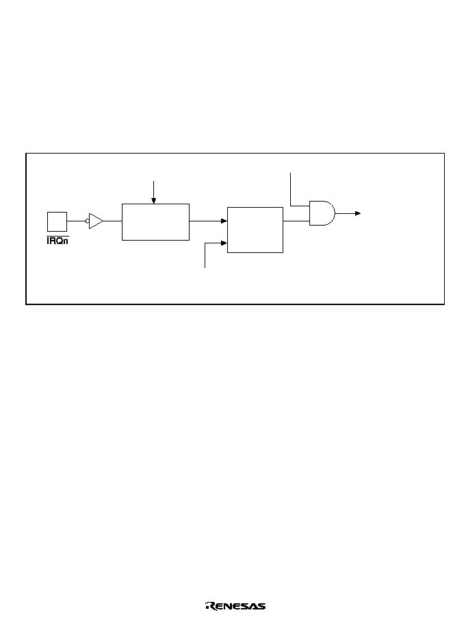
Rev. 2.0, 04/02, page 101 of 906
When IRQ15 to IRQ0 interrupt requests occur at low level of
,54Q, the corresponding ,54 should
be held low until an interrupt handling starts. Then the corresponding
,54 should be set to high in
the interrupt handling routine and clear the IRQnF bit (n = 0 to 15) in ISR to 0. Interrupts may not
be executed when the corresponding
,54 is set to high before the interrupt handling starts.
Detection of IRQ15 to IRQ0 interrupts does not depend on whether the relevant pin has been set
for input or output. However, when a pin is used as an external interrupt input pin, do not clear the
corresponding DDR to 0 and use the pin as an I/O pin for another function.
A block diagram of interrupts IRQ15 to IRQ0 is shown in figure 5.2.
IRQn interrupt
request
IRQnE
IRQnF
S
R
Q
Clear signal
Edge/
level detection
circuit
IRQnSCA, IRQnSCB
input
Note: n = 15 to 0
Figure 5.2 Block Diagram of Interrupts IRQ15 to IRQ0
5.4.2
Internal Interrupts
The sources for internal interrupts from on-chip peripheral modules have the following features:
∑
For each on-chip peripheral module there are flags that indicate the interrupt request status,
and enable bits that select enabling or disabling of these interrupts. They can be controlled
independently. When the enable bit is set to 1, an interrupt request is issued to the interrupt
controller.
∑
The interrupt priority level can be set by means of IPR.
∑
The DMAC and DTC can be activated by a TPU, SCI, or other interrupt request.
∑
When the DMAC or DTC is activated by an interrupt request, it is not affected by the interrupt
control mode or CPU interrupt mask bit.

Rev. 2.0, 04/02, page 102 of 906
5.5
Interrupt Exception Handling Vector Table
Table 5.2 shows interrupt exception handling sources, vector addresses, and interrupt priorities.
For default priorities, the lower the vector number, the higher the priority. When interrupt control
mode 2 is set, priorities among modules can be set by means of the IPR. Modules set at the same
priority will conform to their default priorities. Priorities within a module are fixed.

Rev. 2.0, 04/02, page 103 of 906
Table 5.2
Interrupt Sources, Vector Addresses, and Interrupt Priorities
Vector
Address
*
Interrupt
Source
Origin of
Interrupt
Source
Vector
Number
Advanced
Mode
IPR
Priority
DTC
Activation
DMAC
Activation
External
NMI
7
H'001C
--
High
--
--
pin
IRQ0
16
H'0040
IPRA14 to IPRA12
--
IRQ1
17
H'0044
IPRA10 to IPRA8
--
IRQ2
18
H'0048
IPRA6 to IPRA4
--
IRQ3
19
H'004C
IPRA2 to IPRA0
--
IRQ4
20
H'0050
IPRB14 to IPRB12
--
IRQ5
21
H'0054
IPRB10 to IPRB8
--
IRQ6
22
H'0058
IPRB6 to IPRB4
--
IRQ7
23
H'005C
IPRB2 to IPRB0
--
IRQ8
24
H'0060
IPRC14 to IPRC12
--
IRQ9
25
H'0064
IPRC10 to IPRC8
--
IRQ10
26
H'0068
IPRC6 to IPRC4
--
IRQ11
27
H'006C
IPRC2 to IPRC0
--
IRQ12
28
H'0070
IPRD14 to IPRD12
--
IRQ13
29
H'0074
IPRD10 to IPRD8
--
IRQ14
30
H'0078
IPRD6 to IPRD4
--
IRQ15
31
H'007C
IPRD2 to IPRD0
--
DTC
SWDTEND
32
H'0080
IPRE14 to IPRE12
--
WDT
WOVI
33
H'0084
IPRE10 to IPRE8
--
--
--
Reserved for
system use
34
H'0088
IPRE6 to IPRE4
--
--
Refresh
controller
CMI
35
H'008C
IPRE2 to IPRE0
--
--
36
H'0090
--
--
--
Reserved for
system use
37
H'0094
IPRF14 to IPRF12
--
--
A/D
ADI
38
H'0098
IPRF10 to IPRF8
--
Reserved for
system use
39
H'009C
--
--
TPU_0
TGI0A
40
H'00A0
IPRF6 to IPRF4
TGI0B
41
H'00A4
--
TGI0C
42
H'00A8
Low
--
Rev. 2.0, 04/02, page 104 of 906
Vector
Address
*
Interrupt
Source
Origin of
Interrupt
Source
Vector
Number
Advanced
Mode
IPR
Priority
DTC
Activation
DMAC
Activation
TPU_0
TGI0D
43
H'00AC
High
--
TCI0V
44
H'00B0
--
--
45
H'00B4
--
--
46
H'00B8
--
--
--
Reserved for
system use
47
H'00BC
IPRF6 to IPRF4
--
--
TPU_1
TGI1A
48
H'00C0
IPRF2 to IPRF0
TGI1B
49
H'00C4
--
TCI1V
50
H'00C8
--
--
TCI1U
51
H'00CC
--
--
TPU_2
TGI2A
52
H'00D0
IPRG14 to IPRG12
TGI2B
53
H'00D4
--
TCI2V
54
H'00D8
--
--
TCI2U
55
H'00DC
--
--
TPU_3
TGI3A
56
H'00E0
IPRG10 to IPRG8
TGI3B
57
H'00E4
--
TGI3C
58
H'00E8
--
TGI3D
59
H'00EC
--
TCI3V
60
H'00F0
--
--
61
H'00F4
--
--
62
H'00F8
--
--
--
Reserved for
system use
63
H'00FC
--
--
TPU_4
TGI4A
64
H'0100
IPRG6 to IPRG4
TGI4B
65
H'0104
--
TCI4V
66
H'0108
--
--
TCI4U
67
H'010C
--
--
TPU_5
TGI5A
68
H'0110
IPRG2 to IPRG0
TGI5B
69
H'0114
--
TCI5V
70
H'0118
--
--
TCI5U
71
H'011C
--
--
TMR_0
CMIA0
72
H'0120
IPRH14 to IPRH12
--
CMIB0
73
H'0124
--
OVI0
74
H'0128
Low
--
--
Rev. 2.0, 04/02, page 105 of 906
Vector
Address
*
Interrupt
Source
Origin of
Interrupt
Source
Vector
Number
Advanced
Mode
IPR
Priority
DTC
Activation
DMAC
Activation
--
Reserved for
system use
75
H'012C
High
--
--
TMR_1
CMIA1
76
H'0130
IPRH10 to IPRH8
--
CMIB1
77
H'0134
--
OVI1
78
H'0138
--
--
--
Reserved for
system use
79
H'013C
--
--
DMAC
DMTEND0A
80
H'0140
IPRH6 to IPRH4
--
DMTEND0B
81
H'0144
--
DMTEND1A
82
H'0148
--
DMTEND1B
83
H'014C
--
EXDMAC
EXDMTEND0
84
H'0150
IPRH0 to IPRH0
--
--
EXDMTEND1
85
H'0154
IPRI14 to IPRI12
--
--
EXDMTEND2
86
H'0158
IPRI10 to IPRI8
--
--
EXDMTEND3
87
H'015C
IPRI6 to IPRI4
--
--
SCI_0
ERI0
88
H'0160
IPRI2 to IPRI0
--
--
RXI0
89
H'0164
TXI0
90
H'0168
TEI0
91
H'016C
--
--
SCI_1
ERI1
92
H'0170
IPRJ14 to IPRJ12
--
--
RXI1
93
H'0174
TXI1
94
H'0178
TEI1
95
H'017C
--
--
SCI_2
ERI2
96
H'0180
IPRJ10 to IPRJ8
--
--
RXI2
97
H'0184
--
TXI2
98
H'0188
--
TEI2
99
H'018C
--
--
--
Reserved for
system use
100
H'0190
IPRJ6 to IPRJ4
--
--
101
H'0194
--
--
102
H'0198
--
--
103
H'019C
Low
--
--

Rev. 2.0, 04/02, page 106 of 906
Vector
Address
*
Interrupt
Source
Origin of
Interrupt
Source
Vector
Number
Advanced
Mode
IPR
Priority
DTC
Activation
DMAC
Activation
--
Reserved for
system use
104
H'01A0
IPRJ2 to IPRJ0
High
--
--
105
H'01A4
--
--
106
H'01A8
--
--
107
H'01AC
--
--
108
H'01B0
IPRK14 to IPRK12
--
--
109
H'01B4
--
--
110
H'01B8
--
--
111
H'01BC
--
--
112
H'01C0
IPRK10 to IPRK8
--
--
113
H'01C4
--
--
114
H'01C8
--
--
115
H'01CC
--
--
116
H'01D0
IPRK6 to IPRK4
--
--
117
H'01D4
--
--
118
H'01D8
--
--
119
H'01DC
--
--
120
H'01E0
IPRK2 to IPRK0
--
--
121
H'01E4
--
--
122
H'01E8
--
--
123
H'01EC
--
--
124
H'01F0
--
--
125
H'01F4
--
--
126
H'01F8
--
--
127
H'01EC
Low
--
--
Note: Lower 16 bits of the start address.

Rev. 2.0, 04/02, page 107 of 906
5.6
Interrupt Control Modes and Interrupt Operation
The interrupt controller has two modes: interrupt control mode 0 and interrupt control mode 2.
Interrupt operations differ depending on the interrupt control mode. The interrupt control mode is
selected by INTCR. Table 5.3 shows the differences between interrupt control mode 0 and
interrupt control mode 2.
Table 5.3
Interrupt Control Modes
Interrupt
Priority Setting
Interrupt
Control Mode Registers
Mask Bits Description
0
Default
I
The priorities of interrupt sources are fixed at
the default settings.
Interrupt sources except for NMI is masked by
the I bit.
2
IPR
I2 to I0
8 priority levels except for NMI can be set with
IPR.
8-level interrupt mask control is performed by
bits I2 to I0.
5.6.1
Interrupt Control Mode 0
In interrupt control mode 0, interrupt requests except for NMI is masked by the I bit of CCR in the
CPU. Figure 5.3 shows a flowchart of the interrupt acceptance operation in this case.
1. If an interrupt source occurs when the corresponding interrupt enable bit is set to 1, an
interrupt request is sent to the interrupt controller.
2. If the I bit is set to 1, only an NMI interrupt is accepted, and other interrupt requests are held
pending. If the I bit is cleared, an interrupt request is accepted.
3. Interrupt requests are sent to the interrupt controller, the highest-ranked interrupt according to
the priority system is accepted, and other interrupt requests are held pending.
4. When the CPU accepts an interrupt request, it starts interrupt exception handling after
execution of the current instruction has been completed.
5. The PC and CCR are saved to the stack area by interrupt exception handling. The PC saved on
the stack shows the address of the first instruction to be executed after returning from the
interrupt handling routine.
6. Next, the I bit in CCR is set to 1. This masks all interrupts except NMI.
7. The CPU generates a vector address for the accepted interrupt and starts execution of the
interrupt handling routine at the address indicated by the contents of the vector address in the
vector table.
Rev. 2.0, 04/02, page 108 of 906
Program execution status
Interrupt generated?
NMI
IRQ0
IRQ1
TEI_2
I = 0
Save PC and CCR
I
1
Read vector address
Branch to interrupt handling routine
Yes
No
Yes
Yes
Yes
No
No
No
Yes
Yes
No
Hold
pending
Figure 5.3 Flowchart of Procedure Up to Interrupt Acceptance
in Interrupt Control Mode 0

Rev. 2.0, 04/02, page 109 of 906
5.6.2
Interrupt Control Mode 2
In interrupt control mode 2, mask control is done in eight levels for interrupt requests except for
NMI by comparing the EXR interrupt mask level (I2 to I0 bits) in the CPU and the IPR setting.
Figure 5.4 shows a flowchart of the interrupt acceptance operation in this case.
1. If an interrupt source occurs when the corresponding interrupt enable bit is set to 1, an
interrupt request is sent to the interrupt controller.
2. When interrupt requests are sent to the interrupt controller, the interrupt with the highest
priority according to the interrupt priority levels set in IPR is selected, and lower-priority
interrupt requests are held pending. If a number of interrupt requests with the same priority are
generated at the same time, the interrupt request with the highest priority according to the
priority system shown in table 5.2 is selected.
3. Next, the priority of the selected interrupt request is compared with the interrupt mask level set
in EXR. An interrupt request with a priority no higher than the mask level set at that time is
held pending, and only an interrupt request with a priority higher than the interrupt mask level
is accepted.
4. When the CPU accepts an interrupt request, it starts interrupt exception handling after
execution of the current instruction has been completed.
5. The PC, CCR, and EXR are saved to the stack area by interrupt exception handling. The PC
saved on the stack shows the address of the first instruction to be executed after returning from
the interrupt handling routine.
6. The T bit in EXR is cleared to 0. The interrupt mask level is rewritten with the priority level of
the accepted interrupt.
If the accepted interrupt is NMI, the interrupt mask level is set to H'7.
7. The CPU generates a vector address for the accepted interrupt and starts execution of the
interrupt handling routine at the address indicated by the contents of the vector address in the
vector table.
Rev. 2.0, 04/02, page 110 of 906
Yes
Program execution status
Interrupt generated?
NMI
Level 6 interrupt?
Mask level 5
or below?
Level 7 interrupt?
Mask level 6
or below?
Save PC, CCR, and EXR
Clear T bit to 0
Update mask level
Read vector address
Branch to interrupt handling routine
Hold
pending
Level 1 interrupt?
Mask level 0?
Yes
Yes
No
Yes
Yes
Yes
No
Yes
Yes
No
No
No
No
No
No
Figure 5.4 Flowchart of Procedure Up to Interrupt Acceptance
in Interrupt Control Mode 2
5.6.3
Interrupt Exception Handling Sequence
Figure 5.5 shows the interrupt exception handling sequence. The example shown is for the case
where interrupt control mode 0 is set in advanced mode, and the program area and stack area are
in on-chip memory.

Rev. 2.0, 04/02, page 111 of 906
(14)
(12)
(10)
(6)
(4)
(2)
(1)
(5)
(7)
(9)
(11)
(13)
Interrupt handling
routine instruction
prefetch
Internal
operation
Vector fetch
stack
Instruction
prefetch
Internal
operation
Interrupt
acceptance
Interrupt level determination
Wait for end of instruction
Interrupt
request signal
Internal
address bus
Internal
read signal
Internal
write signal
Internal
data bus
(3)
(1)
(2) (4)
(3)
(5)
(7)
Instruction prefetch address (Not executed.
This is the contents of the saved PC, the return address.)
Instruction code (Not executed.)
Instruction prefetch address (Not executed.)
SP-2
SP-4
Saved PC and saved CCR
Vector address
Interrupt handling routine start address (Vector address contents)
Interrupt handling routine start address ((13) = (10)(12))
First instruction of interrupt handling routine
(6) (8)
(9) (11)
(10) (12)
(13)
(14)
(8)
Figure 5.5 Interrupt Exception Handling

Rev. 2.0, 04/02, page 112 of 906
5.6.4
Interrupt Response Times
Table 5.4 shows interrupt response times - the interval between generation of an interrupt request
and execution of the first instruction in the interrupt handling routine. The execution status
symbols used in table 5.4 are explained in table 5.5.
This LSI is capable of fast word transfer to on-chip memory, and have the program area in on-chip
ROM and the stack area in on-chip RAM, enabling high-speed processing.
Table 5.4
Interrupt Response Times
Normal Mode
*
5
Advanced Mode
No.
Execution Status
Interrupt
control
mode 0
Interrupt
control
mode 2
Interrupt
control
mode 0
Interrupt
control
mode 2
1
Interrupt priority determination
*
1
3
3
3
3
2
Number of wait states until executing
instruction ends
*
2
1 to 19 +2∑S
I
1 to 19+2∑S
I
1 to 19+2∑S
I
1 to 19+2∑S
I
3
PC, CCR, EXR stack save
2∑S
K
3∑S
K
2∑S
K
3∑S
K
4
Vector fetch
S
I
S
I
2∑S
I
2∑S
I
5
Instruction fetch
*
3
2∑S
I
2∑S
I
2∑S
I
2∑S
I
6
Internal processing
*
4
2
2
2
2
Total (using on-chip memory)
11 to 31
12 to 32
12 to 32
13 to 33
Notes: 1. Two states in case of internal interrupt.
2. Refers to MULXS and DIVXS instructions.
3. Prefetch after interrupt acceptance and interrupt handling routine prefetch.
4. Internal processing after interrupt acceptance and internal processing after vector fetch.
5. Not available in this LSI.

Rev. 2.0, 04/02, page 113 of 906
Table 5.5
Number of States in Interrupt Handling Routine Execution Statuses
Object of Access
External Device
8 Bit Bus
16 Bit Bus
Symbol
Internal
Memory
2-State
Access
3-State
Access
2-State
Access
3-State
Access
Instruction fetch S
I
1
4
6+2m
2
3+m
Branch address read S
J
Stack manipulation S
K
Legend:
m: Number of wait states in an external device access.
5.6.5
DTC and DMAC Activation by Interrupt
The DTC and DMAC can be activated by an interrupt. In this case, the following options are
available:
∑
Interrupt request to CPU
∑
Activation request to DTC
∑
Activation request to DMAC
∑
Selection of a number of the above
For details of interrupt requests that can be used to activate the DTC and DMAC, see table 5.2 and
section 9, Data Transfer Controller and section 7, DMA Controller.
Figure 5.6 shows a block diagram of the DTC, DMAC, and interrupt controller.
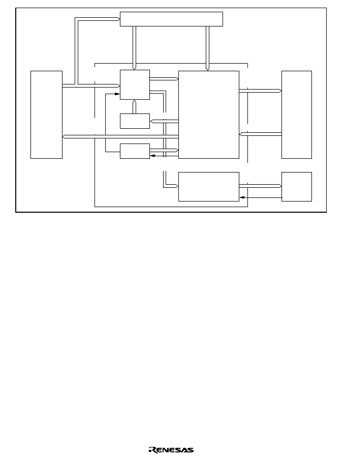
Rev. 2.0, 04/02, page 114 of 906
DMAC
Selection
circuit
DTCER
DTVECR
Control logic
Determination of
priority
CPU
DTC
Select
signal
IRQ
interrupt
On-chip
supporting
module
Disable
signal
Clear signal
Clear signal
Interrupt controller
I, I2 to I0
Interrupt source
clear signal
Interrupt
request
DTC activation
request vector
number
CPU interrupt
request vector
number
SWDTE
clear signal
Clear signal
Figure 5.6 DTC, DMAC, and Interrupt Controller
(1) Selection of Interrupt Source: The activation factors for each channel of DMAC are selected
by DTF3 to DTF0 bits of DMACR. The DTA bit of DMABCR can be used to select whether the
selected activation factors are managed by DMAC. By setting the DTA bit to 1, the interrupt
factor which were the activation factor for that DMAC do not act as the DTC activation factor or
the CPU interrupt factor.
Interrupt factors other than the interrupts managed by the DMAC are selected as DTC activation
source or CPU interrupt source by the DTCE bit of DTCERA to DTCERF of DTC.
By specifying the DISEL bit of the DTC's MRB, it is possible to clear the DTCE bit to 0 after
DTC data transfer, and request a CPU interrupt.
If DTC carries out the designate number of data transfers and the transfer counter reads 0, after
DTC data transfer, the DTCE bit is also cleared to 0, and an interrupt is requested to the CPU.
(2) Determination of Priority: The DTC activation source is selected in accordance with the
default priority order, and is not affected by mask or priority levels. See table 9.1 for the respective
priority. DMAC inputs activation factor directly to each channel.
Rev. 2.0, 04/02, page 115 of 906
(3) Operation Order: If the same interrupt is selected as a DTC activation source and a CPU
interrupt source, the DTC data transfer is performed first, followed by CPU interrupt exception
handling.
If the same interrupt is selected as the DMAC activation factor and as the DTC activation factor or
CPU interrupt factor, these operate independently.
Table 5.6 shows the interrupt factor clear control and selection of interrupt factors by specification
of the DTA bit of DMAC's DMABCR, the DTCE bit of DTC's DTCERA to DTCERH, and the
DISEL bit of DTC's MRB.
Table 5.6
Interrupt Source Selection and Clearing Control
Settings
DMAC
DTC
Interrupt Sources Selection/Clearing Control
DTA
DTCE
DISEL
DMAC
DTC
CPU
0
0
*
X
1
0
X
1
1
*
*
X
X
Legend
: The relevant interrupt is used. Interrupt source clearing is performed.
(The CPU should clear the source flag in the interrupt handling routine.)
: The relevant interrupt is used. The interrupt source is not cleared.
X : The relevant interrupt cannot be used.
*
: Don't care
Note: The SCI or A/D converter interrupt source is cleared when the DMAC or DTC reads or
writes to the prescribed register, and is not dependent upon the DTA bit or DISEL bit.
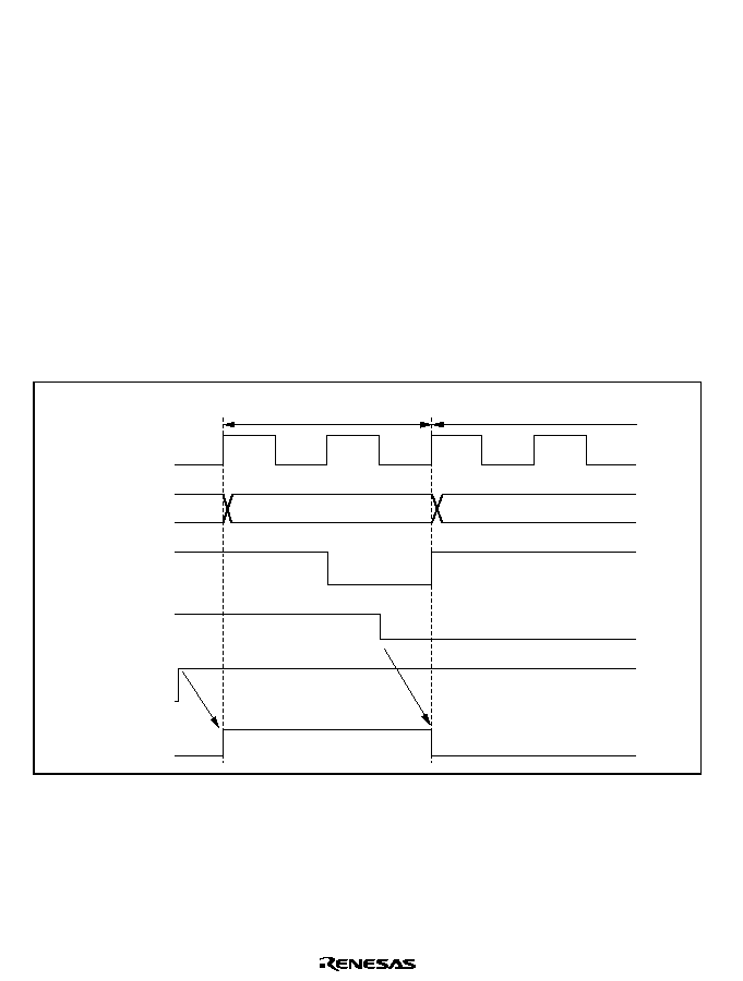
Rev. 2.0, 04/02, page 116 of 906
5.7
Usage Notes
5.7.1
Contention between Interrupt Generation and Disabling
When an interrupt enable bit is cleared to 0 to mask interrupts, the masking becomes effective
after execution of the instruction.
When an interrupt enable bit is cleared to 0 by an instruction such as BCLR or MOV, if an
interrupt is generated during execution of the instruction, the interrupt concerned will still be
enabled on completion of the instruction, and so interrupt exception handling for that interrupt will
be executed on completion of the instruction. However, if there is an interrupt request of higher
priority than that interrupt, interrupt exception handling will be executed for the higher-priority
interrupt, and the lower-priority interrupt will be ignored. The same also applies when an interrupt
source flag is cleared to 0. Figure 5.7 shows an example in which the TCIEV bit in the TPU's
TIER_0 register is cleared to 0. The above contention will not occur if an enable bit or interrupt
source flag is cleared to 0 while the interrupt is masked.
Internal
address bus
Internal
write signal
TCIEV
TCFV
TCIV
interrupt signal
TIER_0 write cycle by CPU
TCIV exception handling
TIER_0 address
Figure 5.7 Contention between Interrupt Generation and Disabling

Rev. 2.0, 04/02, page 117 of 906
5.7.2
Instructions that Disable Interrupts
Instructions that disable interrupts are LDC, ANDC, ORC, and XORC. After any of these
instructions is executed, all interrupts including NMI are disabled and the next instruction is
always executed. When the I bit is set by one of these instructions, the new value becomes valid
two states after execution of the instruction ends.
5.7.3
Times when Interrupts are Disabled
There are times when interrupt acceptance is disabled by the interrupt controller.
The interrupt controller disables interrupt acceptance for a 3-state period after the CPU has
updated the mask level with an LDC, ANDC, ORC, or XORC instruction.
5.7.4
Interrupts during Execution of EEPMOV Instruction
Interrupt operation differs between the EEPMOV.B instruction and the EEPMOV.W instruction.
With the EEPMOV.B instruction, an interrupt request (including NMI) issued during the transfer
is not accepted until the transfer is completed.
With the EEPMOV.W instruction, if an interrupt request is issued during the transfer, interrupt
exception handling starts at a break in the transfer cycle. The PC value saved on the stack in this
case is the address of the next instruction. Therefore, if an interrupt is generated during execution
of an EEPMOV.W instruction, the following coding should be used.
L1: EEPMOV.W
MOV.W R4,R4
BNE L1
5.7.5
Change of IRQ Pin Select Register (ITSR) Setting
When the ITSR setting is changed, an edge occurs internally and the IRQnF bit (n = 0 to 15) of
ISR may be set to 1 at the unintended timing if the selected pin level before the change is different
from the selected pin level after the change. If the IRQn interrupt request (n = 0 to 15) is enabled,
the interrupt exception handling is executed. To prevent the unintended interrupt, ITSR setting
should be changed while the IRQn interrupt request is disabled, then the IRQnF bit should be
cleared to 0.

Rev. 2.0, 04/02, page 118 of 906
5.7.6
Note on IRQ Status Register (ISR)
Since IRQnF flags may be set to 1 depending on the pin states after a reset, be sure to read from
ISR after a reset and then write 0 to clear the IRQnF flags.

Rev. 2.0, 04/02, page 119 of 906
Section 6 Bus Controller (BSC)
This LSI has an on-chip bus controller (BSC) that manages the external address space divided into
eight areas.
The bus controller also has a bus arbitration function, and controls the operation of the internal bus
mastership--the CPU, DMA controller (DMAC), EXDMA controller (EXDMAC), and data
transfer controller (DTC).
6.1
Features
∑
Manages external address space in area units
Manages the external address space divided into eight areas of 2 Mbytes
Bus specifications can be set independently for each area
Burst ROM, DRAM, or synchronous DRAM* interface can be set
∑
Basic bus interface
Chip select signals (
&6 to &6) can be output for areas 0 to 7
8-bit access or 16-bit access can be selected for each area
2-state access or 3-state access can be selected for each area
Program wait states can be inserted for each area
∑
Burst ROM interface
Burst ROM interface can be set independently for areas 0 and 1
∑
DRAM interface
DRAM interface can be set for areas 2 to 5
∑
Synchronous DRAM interface
Continuous synchronous DRAM space can be set for areas 2 to 5
∑
Bus arbitration function
Includes a bus arbiter that arbitrates bus mastership between the CPU, DMAC, and DTC
Note: The Synchronous DRAM interface is not supported in the H8S/2678 Series.
BSCS202A_010020020400
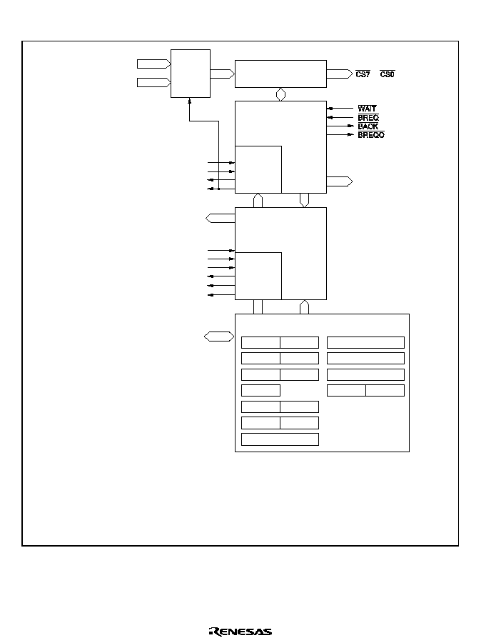
Rev. 2.0, 04/02, page 120 of 906
A block diagram of the bus controller is shown in figure 6.1.
Area decoder
Internal address bus
EXDMAC address bus
to
External bus
control signals
Internal bus control signals
Internal data bus
Control registers
Address
selector
External bus
arbiter
External bus controller
Internal bus
arbiter
Internal bus controller
Internal bus master bus request signal
EXDMAC bus request signal
Internal bus master bus acknowledge signal
EXDMAC bus acknowledge signal
CPU bus request signal
DTC bus request signal
DMAC bus request signal
CPU bus acknowledge signal
DTC bus acknowledge signal
DMAC bus acknowledge signal
ABWCR
ASTCR
WTCRAH WTCRAL
WTCRBH WTCRBL
RDNCR
DRAMCR
Legend
ABWCR
: Bus width control register
ASTCR
: Access state control register
WTCRAH, WTCRAL,
WTCRBH, and WTCRBL : Wait control registers AH, AL, BH, and BL
RDNCR
: Read strobe timing control register
CSACRH and CSACRL : CS assertion period control registers
BROMCRH
: Area 0 burst ROM interface control register
Note:
*
DRACCR is an 8-bit register in the H8S/2678 Series and a 16-bit register in the H8S/2678R Series.
BROMCRL : Area 1 burst ROM interface control register
BCR
: Bus control register
DRAMCR : DRAM control register
DRACCR
: DRAM access control register
REFCR
: Refresh control register
RTCNT
: Refresh timer counter
RTCOR
: Refresh time constant register
REFCR
RTCNT
RTCOR
CSACRH
CSACRL
BROMCRH BROMCRL
BCR
DRACCR
*
Figure 6.1 Block Diagram of Bus Controller

Rev. 2.0, 04/02, page 121 of 906
6.2
Input/Output Pins
Table 6.1 shows the pin configuration of the bus controller.
Table 6.1
Pin Configuration
Name
Symbol
I/O
Function
Address strobe
$6
Output
Strobe signal indicating that basic bus
interface space is accessed and address
output on address bus is enabled.
Read
5'
Output
Strobe signal indicating that basic bus
interface space is being read.
High write/write enable
+:5
Output
Strobe signal indicating that basic bus
interface space is written to, and upper half
(D15 to D8) of data bus is enabled or
DRAM interface space write enable signal.
Low write
/:5
Output
Strobe signal indicating that basic bus
interface space is written to, and lower half
(D7 to D0) of data bus is enabled.
Chip select 0
&6
Output
Strobe signal indicating that area 0 is
selected.
Chip select 1
&6
Output
Strobe signal indicating that area 1 is
selected
Chip select 2/row address
strobe 2/row address strobe
*
&6
/
5$6
/
*
5$6*
Output
Strobe signal indicating that area 2 is
selected, DRAM row address strobe signal
when area 2 is DRAM interface space or
areas 2 to 5 are set as continuous DRAM
interface space, or row address strobe
signal of the synchronous DRAM when the
synchronous DRAM interface is selected.
Chip select 3/row address
strobe 3/column address
strobe
*
&6
/
5$6
/
*
&$6*
Output
Strobe signal indicating that area 3 is
selected, DRAM row address strobe signal
when area 3 is DRAM interface space, or
column address strobe signal of the
synchronous DRAM when the synchronous
DRAM interface is selected.

Rev. 2.0, 04/02, page 122 of 906
Name
Symbol
I/O
Function
Chip select 4/row address
strobe 4/write enable
*
&6
/
5$6
/
*
:(*
Output
Strobe signal indicating that area 4 is
selected, DRAM row address strobe signal
when area 4 is DRAM interface space, or
write enable signal of the synchronous
DRAM when the synchronous DRAM
interface is selected.
Chip select 5/row address
strobe 5/SDRAM
&6
/
5$6
/
*
SDRAM
*
Output
Strobe signal indicating that area 5 is
selected, DRAM row address strobe signal
when area 5 is DRAM interface space, or
dedicated clock signal for the synchronous
DRAM when the synchronous DRAM
interface is selected.
Chip select 6
&6
Output
Strobe signal indicating that area 6 is
selected.
Chip select 7
&6
Output
Strobe signal indicating that area 7 is
selected.
Upper column address
strobe/upper data mask enable
8&$6
/
'408*
Output
16-bit DRAM interface space upper column
address strobe signal, 8-bit DRAM interface
space column address strobe signal, upper
data mask signal of 16-bit synchronous
DRAM interface space, or data mask signal
of 8-bit synchronous DRAM interface
space.
Lower column address strobe/
lower data mask enable
/&$6
/
'40/*
Output
16-bit DRAM interface space lower column
address strobe signal or lower data mask
signal for the 16-bit synchronous DRAM
interface space.
Output enable/clock enable
2(
/CKE
*
Output
Output enable signal for the DRAM
interface space or clock enable signal for
the synchronous DRAM interface space.
Wait
:$,7
Input
Wait request signal when accessing
external space.
Bus request
%5(4
Input
Request signal for release of bus to
external bus master.
Bus request acknowledge
%$&.
Output
Acknowledge signal indicating that bus has
been released to external bus master.

Rev. 2.0, 04/02, page 123 of 906
Name
Symbol
I/O
Function
Bus request output
%5(42
Output
External bus request signal used when
internal bus master accesses external
address space when external bus is
released.
Data transfer acknowledge
1 (DMAC)
'$&.
Output
Data transfer acknowledge signal for single
address transfer by DMAC channel 1.
Data transfer acknowledge
0 (DMAC)
'$&.
'$&.
Data transfer acknowledge signal for single
address transfer by DMAC channel 0.
Data transfer acknowledge
3 (EXDMAC)
('$&.
Output
Data transfer acknowledge signal for single
address transfer by EXDMAC channel 3.
Data transfer acknowledge
2 (EXDMAC)
('$&.
Output
Data transfer acknowledge signal for single
address transfer by EXDMAC channel 2.
Data transfer acknowledge
1 (EXDMAC)
('$&.
Output
Data transfer acknowledge signal for single
address transfer by EXDMAC channel 1.
Data transfer acknowledge
0 (EXDMAC)
('$&.
Output
Data transfer acknowledge signal for single
address transfer by EXDMAC channel 0.
Note: These pins are not supported in the H8S/2678 Series.
6.3
Register Descriptions
The bus controller has the following registers.
∑
Bus width control register (ABWCR)
∑
Access state control register (ASTCR)
∑
Wait control register AH (WTCRAH)
∑
Wait control register AL (WTCRAL)
∑
Wait control register BH (WTCRBH)
∑
Wait control register BL (WTCRBL)
∑
Read strobe timing control register (RDNCR)
∑
&6 assertion period control register H (CSACRH)
∑
&6 assertion period control register L (CSACRL)
∑
Area 0 burst ROM interface control register (BROMCRH)
∑
Area 1 burst ROM interface control register (BROMCRL)
∑
Bus control register (BCR)
∑
DRAM control register (DRAMCR)
∑
DRAM access control register (DRACCR)
∑
Refresh control register (REFCR)
∑
Refresh timer counter (RTCNT)

Rev. 2.0, 04/02, page 124 of 906
∑
Refresh time constant register (RTCOR)
6.3.1
Bus Width Control Register (ABWCR)
ABWCR designates each area in the external address space as either 8-bit access space or 16-bit
access space.
Bit
Bit Name
Initial Value
*
R/W
Description
7
6
5
4
3
2
1
0
ABW7
ABW6
ABW5
ABW4
ABW3
ABW2
ABW1
ABW0
1/0
1/0
1/0
1/0
1/0
1/0
1/0
1/0
R/W
R/W
R/W
R/W
R/W
R/W
R/W
R/W
Area 7 to 0 Bus Width Control
These bits select whether the corresponding
area is to be designated as 8-bit access space
or 16-bit access space.
0: Area n is designated as 16-bit access space
1: Area n is designated as 8-bit access space
(n = 7 to 0)
Note: In modes 2, 4, and 6, ABWCR is initialized to 1. In modes 1, 5, and 7, ABWCR is initialized
to 0.
6.3.2
Access State Control Register (ASTCR)
ASTCR designates each area in the external address space as either 2-state access space or 3-state
access space.
Bit
Bit Name
Initial Value
R/W
Description
7
6
5
4
3
2
1
0
AST7
AST6
AST5
AST4
AST3
AST2
AST1
AST0
1
1
1
1
1
1
1
1
R/W
R/W
R/W
R/W
R/W
R/W
R/W
R/W
Area 7 to 0 Access State Control
These bits select whether the corresponding
area is to be designated as 2-state access
space or 3-state access space. Wait state
insertion is enabled or disabled at the same
time.
0: Area n is designated as 2-state access space
Wait state insertion in area n access is disabled
1: Area n is designated as 3-state access space
Wait state insertion in area n access is enabled
(n = 7 to 0)

Rev. 2.0, 04/02, page 125 of 906
6.3.3
Wait Control Registers AH, AL, BH, and BL (WTCRAH, WTCRAL, WTCRBH,
and WTCRBL)
WTCRA and WTCRB select the number of program wait states for each area in the external
address space.
In addition, CAS latency is set when a synchronous DRAM is connected.
∑
WTCRAH
Bit
Bit Name
Initial Value
R/W
Description
15
-
0
R
Reserved
This bit is always read as 0 and cannot be
modified.
14
13
12
W72
W71
W70
1
1
1
R/W
R/W
R/W
Area 7 Wait Control 2 to 0
These bits select the number of program wait
states when accessing area 7 while AST7 bit in
ASTCR = 1.
000: Program wait not inserted
001: 1 program wait state inserted
010: 2 program wait states inserted
011: 3 program wait states inserted
100: 4 program wait states inserted
101: 5 program wait states inserted
110: 6 program wait states inserted
111: 7 program wait states inserted
11
-
0
R
Reserved
This bit is always read as 0 and cannot be
modified.

Rev. 2.0, 04/02, page 126 of 906
Bit
Bit Name
Initial Value
R/W
Description
10
9
8
W62
W61
W60
1
1
1
R/W
R/W
R/W
Area 6 Wait Control 2 to 0
These bits select the number of program wait
states when accessing area 6 while AST6 bit in
ASTCR = 1.
000: Program wait not inserted
001: 1 program wait state inserted
010: 2 program wait states inserted
011: 3 program wait states inserted
100: 4 program wait states inserted
101: 5 program wait states inserted
110: 6 program wait states inserted
111: 7 program wait states inserted
∑
WTARAL
Bit
Bit Name
Initial Value
R/W
Description
7
-
0
R
Reserved
This bit is always read as 0 and cannot be
modified.
6
5
4
W52
W51
W50
1
1
1
R/W
R/W
R/W
Area 5 Wait Control 2 to 0
These bits select the number of program wait
states when accessing area 5 while AST5 bit in
ASTCR = 1.
000: Program wait not inserted
001: 1 program wait state inserted
010: 2 program wait states inserted
011: 3 program wait states inserted
100: 4 program wait states inserted
101: 5 program wait states inserted
110: 6 program wait states inserted
111: 7 program wait states inserted

Rev. 2.0, 04/02, page 127 of 906
Bit
Bit Name
Initial Value
R/W
Description
3
-
0
R
Reserved
This bit is always read as 0 and cannot be
modified.
2
1
0
W42
W41
W40
1
1
1
R/W
R/W
R/W
Area 4 Wait Control 2 to 0
These bits select the number of program wait
states when accessing area 4 while AST4 bit in
ASTCR = 1.
000: Program wait not inserted
001: 1 program wait state inserted
010: 2 program wait states inserted
011: 3 program wait states inserted
100: 4 program wait states inserted
101: 5 program wait states inserted
110: 6 program wait states inserted
111: 7 program wait states inserted
∑
WTCRBH
Bit
Bit Name
Initial Value
R/W
Description
15
-
0
R
Reserved
This bit is always read as 0 and cannot be
modified.
14
13
12
W32
W31
W30
1
1
1
R/W
R/W
R/W
Area 3 Wait Control 2 to 0
These bits select the number of program wait
states when accessing area 3 while AST3 bit in
ASTCR = 1.
000: Program wait not inserted
001: 1 program wait state inserted
010: 2 program wait states inserted
011: 3 program wait states inserted
100: 4 program wait states inserted
101: 5 program wait states inserted
110: 6 program wait states inserted
111: 7 program wait states inserted
11
-
0
R
Reserved
This bit is always read as 0 and cannot be
modified.

Rev. 2.0, 04/02, page 128 of 906
Bit
Bit Name
Initial Value
R/W
Description
10
9
8
W22
W21
W20
1
1
1
R/W
R/W
R/W
Area 2 Wait Control 2 to 0
These bits select the number of program wait
states when accessing area 2 while AST2 bit in
ASTCR = 1.
A CAS latency is set when the synchronous
DRAM is connected
*
. The setting of area 2 is
reflected to the setting of areas 2 to 5. A CAS
latency can be set regardless of whether or not
an ASTCR wait state insertion is enabled.
000: Program wait not inserted
001: 1 program wait state inserted
010: 2 program wait states inserted
011: 3 program wait states inserted
100: 4 program wait states inserted
101: 5 program wait states inserted
110: 6 program wait states inserted
111: 7 program wait states inserted
000: Synchronous DRAM of CAS latency 1 is
connected to areas 2 to 5.
001: Synchronous DRAM of CAS latency 2 is
connected to areas 2 to 5.
010: Synchronous DRAM of CAS latency 3 is
connected to areas 2 to 5.
011: Synchronous DRAM of CAS latency 4 is
connected to areas 2 to 5.
1XXX: Setting prohibited.
Note: The synchronous DRAM interface is not supported in the H8S/2678 Series.
Legend x: Don't care.

Rev. 2.0, 04/02, page 129 of 906
∑
WTCRBL
Bit
Bit Name
Initial Value
R/W
Description
7
-
0
R
Reserved
This bit is always read as 0 and cannot be
modified.
6
5
4
W12
W11
W10
1
1
1
R/W
R/W
R/W
Area 1 Wait Control 2 to 0
These bits select the number of program wait
states when accessing area 1 while AST1 bit in
ASTCR = 1.
000: Program wait not inserted
001: 1 program wait state inserted
010: 2 program wait states inserted
011: 3 program wait states inserted
100: 4 program wait states inserted
101: 5 program wait states inserted
110: 6 program wait states inserted
111: 7 program wait states inserted
3
-
0
R
Reserved
This bit is always read as 0 and cannot be
modified.
2
1
0
W02
W01
W00
1
1
1
R/W
R/W
R/W
Area 0 Wait Control 2 to 0
These bits select the number of program wait
states when accessing area 0 while AST0 bit in
ASTCR = 1.
000: Program wait not inserted
001: 1 program wait state inserted
010: 2 program wait states inserted
011: 3 program wait states inserted
100: 4 program wait states inserted
101: 5 program wait states inserted
110: 6 program wait states inserted
111: 7 program wait states inserted
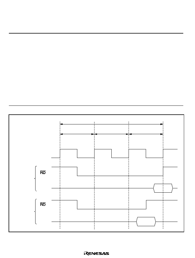
Rev. 2.0, 04/02, page 130 of 906
6.3.4
Read Strobe Timing Control Register (RDNCR)
RDNCR selects the read strobe signal (
5') negation timing in a basic bus interface read access.
Bit
Bit Name
Initial Value
R/W
Description
7
6
5
4
3
2
1
0
RDN7
RDN6
RDN5
RDN4
RDN3
RDN2
RDN1
RDN0
0
0
0
0
0
0
0
0
R/W
R/W
R/W
R/W
R/W
R/W
R/W
R/W
Read Strobe Timing Control 7 to 0
These bits set the negation timing of the read
strobe in a corresponding area read access.
As shown in figure 6.2, the read strobe for an
area for which the RDNn bit is set to 1 is
negated one half-state earlier than that for an
area for which the RDNn bit is cleared to 0. The
read data setup and hold time specifications are
also one half-state earlier.
0: In an area n read access, the
5'
is negated
at the end of the read cycle
1: In an area n read access, the
5'
is negated
one half-state before the end of the read cycle
(n = 7 to 0)
Bus cycle
T
1
T
2
Data
Data
RDNn = 0
RDNn = 1
T
3
Figure 6.2 Read Strobe Negation Timing (Example of 3-State Access Space)

Rev. 2.0, 04/02, page 131 of 906
6.3.5
$
$ Assertion Period Control Registers H, L (CSACRH, CSACRL)
CSACRH and CSACRL select whether or not the assertion period of the basic bus interface chip
select signals (
&6Q) and address signals is to be extended. Extending the assertion period of the
&6Q and address signals allows flexible interfacing to external I/O devices.
∑
CSACRH
Bit
Bit Name
Initial Value
R/W
Description
7
6
5
4
3
2
1
0
CSXH7
CSXH6
CSXH5
CSXH4
CSXH3
CSXH2
CSXH1
CSXH0
0
0
0
0
0
0
0
0
R/W
R/W
R/W
R/W
R/W
R/W
R/W
R/W
&6
and Address Signal Assertion Period
Control 1
These bits specify whether or not the T
h
cycle is
to be inserted (see figure 6.3). When an area for
which the CSXHn bit is set to 1 is accessed, a
one-state T
h
cycle, in which only the
&6Q
and
address signals are asserted, is inserted before
the normal access cycle.
0: In area n basic bus interface access, the
&6Q
and address assertion period (T
h
) is not
extended
1: In area n basic bus interface access, the
&6Q
and address assertion period (T
h
) is extended
(n = 7 to 0)
∑
CSACRL
Bit
Bit Name
Initial Value
R/W
Description
7
6
5
4
3
2
1
0
CSXT7
CSXT6
CSXT5
CSXT4
CSXT3
CSXT2
CSXT1
CSXT0
0
0
0
0
0
0
0
0
R/W
R/W
R/W
R/W
R/W
R/W
R/W
R/W
&6
and Address Signal Assertion Period
Control 2
These bits specify whether or not the T
t
cycle
shown in figure 6.3 is to be inserted. When an
area for which the CSXTn bit is set to 1 is
accessed, a one-state T
t
cycle, in which only the
&6Q
and address signals are asserted, is
inserted before the normal access cycle.
0: In area n basic bus interface access, the
&6Q
and address assertion period (T
t
) is not
extended
1: In area n basic bus interface access, the
&6Q
and address assertion period (T
t
) is extended
(n = 7 to 0)
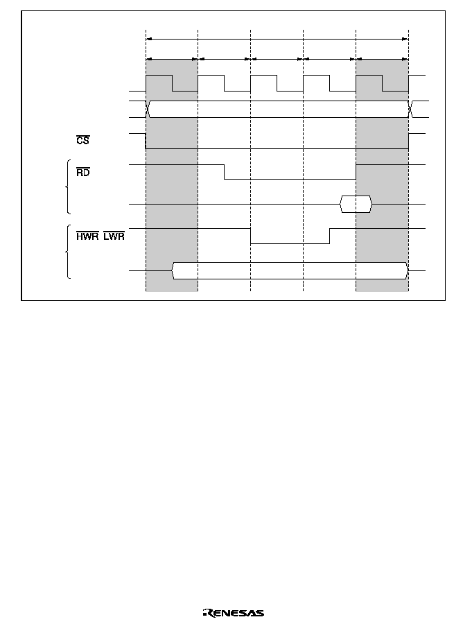
Rev. 2.0, 04/02, page 132 of 906
T
h
Address
T
1
T
2
T
3
T
t
Bus cycle
Data
,
Write
Data
Read
Figure 6.3
$$ and Address Assertion Period Extension (Example of 3-State Access Space
and RDNn = 0)

Rev. 2.0, 04/02, page 133 of 906
6.3.6
Area 0 Burst ROM Interface Control Register (BROMCRH)
Area 1 Burst ROM Interface Control Register (BROMCRL)
BROMCRH and BROMCRL are used to make burst ROM interface settings. Area 0 and area 1
burst ROM interface settings can be made independently in BROMCRH and BROMCRL,
respectively.
Bit
Bit Name
Initial Value
R/W
Description
7
BSRMn
0
R/W
Burst ROM Interface Select
Selects the basic bus interface or burst ROM
interface.
0: Basic bus interface space
1: Burst ROM interface space
6
5
4
BSTSn2
BSTSn1
BSTSn0
0
0
0
R/W
R/W
R/W
Burst Cycle Select
These bits select the number of burst cycle
states.
000: 1 state
001: 2 states
010: 3 states
011: 4 states
100: 5 states
101: 6 states
110: 7 states
111: 8 states
3
2
-
-
0
0
R/W
R/W
Reserved
These bits are always read as 0. The initial
value should not be changed.
1
0
BSWDn1
BSWDn0
0
0
R/W
R/W
Burst Word Number Select
These bits select the number of words that can
be burst-accessed on the burst ROM interface.
00: Maximum 4 words
01: Maximum 8 words
10: Maximum 16 words
11: Maximum 32 words
(n = 1 or 0)

Rev. 2.0, 04/02, page 134 of 906
6.3.7
Bus Control Register (BCR)
BCR is used for idle cycle settings, selection of the external bus released state protocol, enabling
or disabling of the write data buffer function, and enabling or disabling of
:$,7 pin input.
Bit
Bit Name
Initial Value
R/W
Description
15
BRLE
0
R/W
External Bus Release Enable
Enables or disables external bus release.
0: External bus release disabled
%5(4
,
%$&.
, and
%5(42
pins can be used
as I/O ports
1: External bus release enabled
14
BREQOE
0
R/W
%5(42
Pin Enable
Controls outputting the bus request signal
(BREQO) to the external bus master in the
external bus released state, when an internal
bus master performs an external address space
access, or when a refresh request is generated.
0:
%5(42
output disabled
%5(42
pin can be used as I/O port
1:
%5(42
output enabled
13
-
0
R/W
Reserved
This bit can be read from or written to. However,
the write value should always be 0.
12
IDLC
1
R/W
Idle Cycle State Number Select
Specifies the number of states in the idle cycle
set by ICIS2, ICIS1, and ICIS0.
0: Idle cycle comprises 1 state
1: Idle cycle comprises 2 states
11
ICIS1
1
R/W
Idle Cycle Insert 1
When consecutive external read cycles are
performed in different areas, an idle cycle can
be inserted between the bus cycles.
0: Idle cycle not inserted
1: Idle cycle inserted

Rev. 2.0, 04/02, page 135 of 906
Bit
Bit Name
Initial Value
R/W
Description
10
ICIS0
1
R/W
Idle Cycle Insert 0
When an external read cycle and external write
cycle are performed consecutively, an idle cycle
can be inserted between the bus cycles.
0: Idle cycle not inserted
1: Idle cycle inserted
9
WDBE
0
R/W
Write Data Buffer Enable
The write data buffer function can be used for
an external write cycle or DMAC single address
transfer cycle.
0: Write data buffer function not used
1: Write data buffer function used
8
WAITE
0
R/W
:$,7
Pin Enable
Selects enabling or disabling of wait input by the
:$,7
pin.
0: Wait input by
:$,7
pin disabled
:$,7
pin can be used as I/O port
1: Wait input by
:$,7
pin enabled
7
to
3
-
0
R/W
Reserved
These are readable/writable bits, but the write
value should always be 0.
2
ICIS2
0
R/W
Idle Cycle Insert 2
When an external write cycle and external read
cycle are performed consecutively, an idle cycle
can be inserted between the bus cycles.
0: Idle cycle not inserted
1: Idle cycle inserted
Note: Bit 2 is a reserved bit in the H8S/2678
Series. This bit is readable/writable, but
the write value should always be 0.
1
to
0
-
0
R/W
Reserved
These bits can be read from or written to.
However, the write value should always be 0.

Rev. 2.0, 04/02, page 136 of 906
6.3.8
DRAM Control Register (DRAMCR)
DRAMCR is used to make DRAM/synchronous DRAM* interface settings.
Note:
The synchronous DRAM interface is not supported in the H8S/2678 Series.
Bit
Bit Name
Initial Value
R/W
Description
15
OEE
0
R/W
2(
Output Enable
The OE signal used when EDO page mode
DRAM is connected can be output from the
(OE) pin. The
2(
signal is common to all areas
designated as DRAM space.
When the synchronous DRAM is connected, the
CKE signal can be output from the (OE) pin.
The CKE signal is common to the continuous
synchronous DRAM space.
0:
2(
/CKE signal output disabled
(
2(
)/(CKE) pin can be used as I/O port
1:
2(
/CKE signal output enabled
14
RAST
0
R/W
5$6
Assertion Timing Select
Selects whether, in DRAM access, the
5$6
signal is asserted from the start of the T
r
cycle
(rising edge of ¯) or from the falling edge of ¯.
Figure 6.4 shows the relationship between the
RAST bit setting and the
5$6
assertion timing.
The setting of this bit applies to all areas
designated as DRAM space.
0:
5$6
is asserted from ¯ falling edge in T
r
cycle
1:
5$6
is asserted from start of T
r
cycle
13
-
0
R/W
Reserved
This bit can be read from or written to. However,
the write value should always be 0.

Rev. 2.0, 04/02, page 137 of 906
Bit
Bit Name
Initial Value
R/W
Description
12
CAST
0
R/W
Column Address Output Cycle Number Select
Selects whether the column address output
cycle in DRAM access comprises 3 states or 2
states. The setting of this bit applies to all areas
designated as DRAM space.
0: 2 states
1: 3 states
11
-
0
R/W
Reserved
This bit can be read from or written to. However,
the write value should always be 0.
10
9
8
RMTS2
RMTS1
RMTS0
0
0
0
R/W
R/W
R/W
DRAM/Continuous Synchronous DRAM Space
Select
These bits designate DRAM/continuous
synchronous DRAM space for areas 2 to 5.
When continuous DRAM space is set, it is
possible to connect large-capacity DRAM
exceeding 2 Mbytes per area. In this case, the
5$6
signal is output from the
&6
pin.
When continuous synchronous DRAM space is
set, it is possible to connect large-capacity
synchronous DRAM exceeding 2 Mbytes per
area. In this case, the
5$6
,
&$6
, and
:(
signals are output from
&6
,
&6
, and
&6
pins, respectively. When synchronous DRAM
mode is set, the mode registers of the
synchronous DRAM can be set.
000: Normal space
001: Normal space in areas 3 to 5
DRAM space in area 2
010: Normal space in areas 4 and 5
DRAM space in areas 2 and 3
011: DRAM space in areas 2 to 5
100: Continuous synchronous DRAM space
(setting prohibited in the H8S/2678 Series)
101: Synchronous DRAM mode setting (setting
prohibited in the H8S/2678 Series)
110: Setting prohibited
111: Continuous DRAM space in areas 2 to 5

Rev. 2.0, 04/02, page 138 of 906
Bit
Bit Name
Initial Value
R/W
Description
7
BE
0
R/W
Burst Access Enable
Selects enabling or disabling of burst access to
areas designated as DRAM/continuous
synchronous DRAM space. DRAM/continuous
synchronous DRAM space burst access is
performed in fast page mode. When using EDO
page mode DRAM, the
2(
signal must be
connected.
0: Full access
1: Access in fast page mode
6
RCDM
0
R/W
5$6
Down Mode
When access to DRAM space is interrupted by
an access to normal bus space, an access to an
internal I/O register, etc., this bit selects whether
the
5$6
signal is held low while waiting for the
next DRAM access (
5$6
down mode), or is
driven high again (
5$6
up mode). The setting
of this bit is valid only when the BE bit is set to
1.
If this bit is cleared to 0 when set to 1 in the
5$6
down state, the
5$6
down state is cleared
at that point, and
5$6
goes high.
When continuous synchronous DRAM space is
set, reading from and writing to this bit is
enabled. However, the setting does not affect
the operation.
0:
5$6
up mode selected for DRAM space
access
1:
5$6
down mode selected for DRAM space
access

Rev. 2.0, 04/02, page 139 of 906
Bit
Bit Name
Initial Value
R/W
Description
5
DDS
0
R/W
DMAC Single Address Transfer Option
Selects whether full access is always performed
or burst access is enabled when DMAC single
address transfer is performed on the
DRAM/synchronous DRAM interface.
When the BE bit is cleared to 0 in DRAMCR,
disabling DRAM/synchronous DRAM burst
access, DMAC single address transfer is
performed in full access mode regardless of the
setting of this bit.
This bit has no effect on other bus master
external accesses or DMAC dual address
transfers.
0: Full access is always executed
1: Burst access is enabled
4
EDDS
0
R/W
EXDMAC Single Address Transfer Option
Selects whether full access is always performed
or burst access is enabled when EXDMAC
single address transfer is performed on the
DRAM/synchronous DRAM interface.
When the BE bit is cleared to 0 in DRAMCR,
disabling DRAM/synchronous DRAM burst
access, EXDMAC single address transfer is
performed in full access mode regardless of the
setting of this bit.
This bit has no effect on other bus master
external accesses or EXDMAC dual address
transfers.
0: Full access is always executed
1: Burst access is enabled
3
-
0
R/W
Reserved
This bit can be read from or written to. However,
the write value should always be 0.

Rev. 2.0, 04/02, page 140 of 906
Bit
Bit Name
Initial Value
R/W
Description
2
1
0
MXC2
MXC1
MXC0
0
0
0
R/W
R/W
R/W
Address Multiplex Select
These bits select the size of the shift toward the
lower half of the row address in row
address/column address multiplexing. In burst
operation on the DRAM/synchronous DRAM
interface, these bits also select the row address
bits to be used for comparison.
When the MXC2 bit is set to 1 while continuous
synchronous DRAM space is set, the address
precharge setting command (Precharge-sel) is
output to the upper column address. For details,
refer to sections 6.6.2 and 6.7.2, Address
Multiplexing.
DRAM interface
000: 8-bit shift
∑
When 8-bit access space is designated:
Row address bits A23 to A8 used for
comparison
∑
When 16-bit access space is designated:
Row address bits A23 to A9 used for
comparison
001: 9-bit shift
∑
When 8-bit access space is designated:
Row address bits A23 to A9 used for
comparison
∑
When 16-bit access space is designated:
Row address bits A23 to A10 used for
comparison
010: 10-bit shift
∑
When 8-bit access space is designated:
Row address bits A23 to A10 used for
comparison
∑
When 16-bit access space is designated:
Row address bits A23 to A11 used for
comparison

Rev. 2.0, 04/02, page 141 of 906
Bit
Bit Name
Initial Value
R/W
Description
011: 11-bit shift
∑
When 8-bit access space is designated:
Row address bits A23 to A11 used for
comparison
When 16-bit access space is designated:
Row address bits A23 to A12 used for
comparison
Synchronous DRAM interface
100: 8-bit shift
∑
When 8-bit access space is designated:
Row address bits A23 to A8 used for
comparison
∑
When 16-bit access space is designated:
Row address bits A23 to A9 used for
comparison
The precharge-sel is A15 to A9 of the
column address.
101: 9-bit shift
∑
When 8-bit access space is designated:
Row address bits A23 to A9 used for
comparison
∑
When 16-bit access space is designated:
Row address bits A23 to A10 used for
comparison
The precharge-sel is A15 to A10 of the
column address.
110: 10-bit shift
∑
When 8-bit access space is designated:
Row address bits A23 to A10 used for
comparison
∑
When 16-bit access space is designated:
Row address bits A23 to A11 used for
comparison
The precharge-sel is A15 to A11 of the
column address.
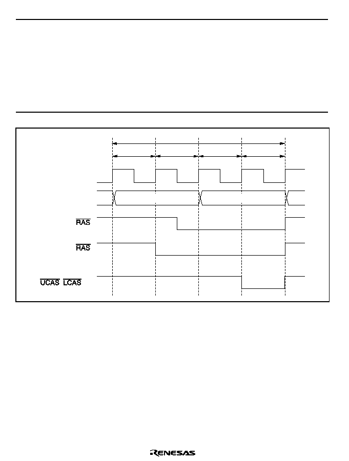
Rev. 2.0, 04/02, page 142 of 906
Bit
Bit Name
Initial Value
R/W
Description
111: 11-bit shift
∑
When 8-bit access space is designated:
Row address bits A23 to A11 used for
comparison
∑
When 16-bit access space is designated:
Row address bits A23 to A12 used for
comparison
The precharge-sel is A15 to A12 of the
column address.
T
p
Address
RAST = 0
RAST = 1
T
r
T
c1
T
c2
,
Bus cycle
Row address
Column address
Figure 6.4
#
#$$ Signal Assertion Timing
(2-State Column Address Output Cycle, Full Access)

Rev. 2.0, 04/02, page 143 of 906
6.3.9
DRAM Access Control Register (DRACCR)
DRACCR is used to set the DRAM/synchronous DRAM interface bus specifications.
Note:
The synchronous DRAM interface is not supported in the H8S/2678 Series.
∑
H8S/2678 Series
Bit
Bit Name
Initial Value
R/W
Description
7
DRMI
0
R/W
Idle Cycle Insertion
An idle cycle can be inserted after a DRAM read
cycle when a continuous normal space access
cycle follows a DRAM read cycle. Idle cycle
insertion conditions, setting of number of states,
etc., comply with settings of bits ICIS1, ICIS0,
and IDLC in BCR register
0: Idle cycle not inserted
1: Idle cycle inserted
6
-
0
R/W
Reserved
This bit can be read from or written to. However,
the write value should always be 0.
5
4
TPC1
TPC0
0
0
R/W
R/W
Precharge State Control
These bits select the number of states in the
RAS precharge cycle in normal access and
refreshing.
00: 1 state
01: 2 states
10: 3 states
11: 4 states
3
2
-
-
0
0
R/W
R/W
Reserved
These bits can be read from or written to.
However, the write value should always be 0.
1
0
RCD1
RCD0
0
0
R/W
R/W
RAS-CAS Wait Control
These bits select a wait cycle to be inserted
between the
5$6
assert cycle and
&$6
assert
cycle.
00: Wait cycle not inserted
01: 1-state wait cycle inserted
10: 2-state wait cycle inserted
11: 3-state wait cycle inserted

Rev. 2.0, 04/02, page 144 of 906
∑
H8S/2678R Series
Bit
Bit Name
Initial Value
R/W
Description
15
DRMI
0
R/W
Idle Cycle Insertion
An idle cycle can be inserted after a
DRAM/synchronous DRAM access cycle when
a continuous normal space access cycle follows
a DRAM/synchronous DRAM access cycle. Idle
cycle insertion conditions, setting of number of
states, etc., comply with settings of bits ICIS2,
ICIS1, ICIS0, and IDLC in BCR register
0: Idle cycle not inserted
1: Idle cycle inserted
14
-
0
R/W
Reserved
This bit can be read from or written to. However,
the write value should always be 0.
13
12
TPC1
TPC0
0
0
R/W
R/W
Precharge State Control
These bits select the number of states in the
RAS precharge cycle in normal access and
refreshing.
00: 1 state
01: 2 states
10: 3 states
11: 4 states
11
SDWCD
0
R/W
CAS Latency Control Cycle Disabled during
Continuous Synchronous DRAM Space Write
Access
Disables CAS latency control cycle (Tc1)
inserted by WTCR settings during synchronous
DRAM write access (see figure 6.5).
0: Enables CAS latency control cycle
1: Disables CAS latency control cycle
10
--
0
R/W
Reserved
This bit can be read from or written to. However,
the write value should always be 0.

Rev. 2.0, 04/02, page 145 of 906
Bit
Bit Name
Initial Value
R/W
Description
9
8
RCD1
RCD0
0
0
R/W
R/W
RAS-CAS Wait Control
These bits select a wait cycle to be inserted
between the
5$6
assert cycle and
&$6
assert
cycle. A 1- to 4-state wait cycle can be inserted.
00: Wait cycle not inserted
01: 1-state wait cycle inserted
10: 2-state wait cycle inserted
11: 3-state wait cycle inserted
7 to 4
--
0
R/W
Reserved
These bits can be read from or written to.
However, the write value should always be 0.
3
CKSPE
0
R/W
Clock Suspend Enable
Enables clock suspend mode for extend read
data during DMAC and EXDMAC single
address transfer with the synchronous DRAM
interface.
0: Disables clock suspend mode
1: Enables clock suspend mode
2
--
0
R/W
Reserved
This bit can be read from or written to. However,
the write value should always be 0.
1
0
RDXC1
RDXC0
0
0
R/W
R/W
Read Data Extension Cycle Number Selection
Selects the number of read data extension cycle
(Tsp) insertion state in clock suspend mode.
These bits are valid when the CKSPE bit is set
to 1.
00: Inserts 1state
01: Inserts 2state
10: Inserts 3state
11: Inserts 4state
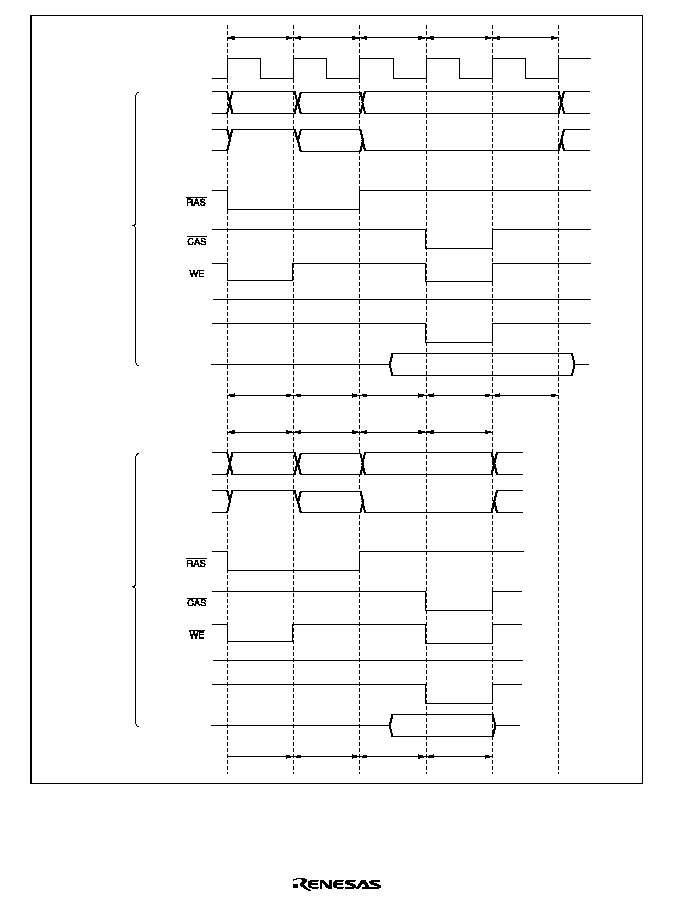
Rev. 2.0, 04/02, page 146 of 906
T
p
¯
SDWCD 0
DQMU, DQML
CKE
Data bus
Address bus
T
r
T
c1
T
cl
T
c2
PALL
ACTV
NOP
WRIT
NOP
T
p
T
r
T
c1
T
c2
Column address
Column address
Row address
Precharge-sel
Row address
Column address
High
SDWCD 1
DQMU, DQML
CKE
Data bus
Address bus
PALL
ACTV
NOP
WRIT
Row address
Precharge-sel
Row address
Column address
High
Figure 6.5 CAS Latency Control Cycle Disable Timing during Continuous Synchronous
DRAM Space Write Access (for CAS Latency 2)

Rev. 2.0, 04/02, page 147 of 906
6.3.10
Refresh Control Register (REFCR)
REFCR specifies DRAM/synchronous DRAM interface refresh control.
Note:
The synchronous DRAM interface is not supported in the H8S/2678 Series.
Bit
Bit Name
Initial Value
R/W
Description
15
CMF
0
R/(W)
*
Compare Match Flag
Status flag that indicates a match between the
values of RTCNT and RTCOR.
[Clearing conditions]
∑
When 0 is written to CMF after reading CMF
= 1 while the RFSHE bit is cleared to 0
∑
When CBR refreshing is executed while the
RFSHE bit is set to 1
[Setting condition]
When RTCOR = RTCNT
14
CMIE
0
R/W
Compare Match Interrupt Enable
Enables or disables interrupt requests (CMI) by
the CMF flag when the CMF flag is set to 1.
This bit is valid when refresh control is not
performed. When the refresh control is
performed, this bit is always cleared to 0 and
cannot be modified.
0: Interrupt request by CMF flag disabled
1: Interrupt request by CMF flag enabled
13
12
RCW1
RCW0
0
0
R/W
R/W
&$6
-
5$6
Wait Control
These bits select the number of wait cycles to
be inserted between the
&$6
assert cycle and
5$6
assert cycle in a DRAM/synchronous
DRAM
refresh cycle.
00: Wait state not inserted
01: 1 wait state inserted
10: 2 wait states inserted
11: 3 wait states inserted
Note: Only 0 can be written, to clear the flag.

Rev. 2.0, 04/02, page 148 of 906
Bit
Bit Name
Initial Value
R/W
Description
11
-
0
R/W
Reserved
This bit can be read from or written to. However,
the write value should always be 0.
10
9
8
RTCK2
RTCK1
RTCK0
0
0
0
R/W
R/W
R/W
Refresh Counter Clock Select
These bits select the clock to be used to
increment the refresh counter. When the input
clock is selected with bits RTCK2 to RTCK0, the
refresh counter begins counting up.
000: Count operation halted
001: Count on ¯/2
010: Count on ¯/8
011: Count on ¯/32
100: Count on ¯/128
101: Count on ¯/512
110: Count on ¯/2048
111: Count on ¯/4096
7
RFSHE
0
R/W
Refresh Control
Refresh control can be performed. When
refresh control is not performed, the refresh
timer can be used as an interval timer.
0: Refresh control is not performed
1: Refresh control is performed
6
CBRM
0
R/W
CBR Refresh Control
Selects CBR refreshing performed in parallel
with other external accesses, or execution of
CBR refreshing alone.
When the continuous synchronous DRAM
space is set, this bit can be read/written, but the
setting contents do not affect operations.
0: External access during CAS-before-RAS
refreshing is enabled
1: External access during CAS-before-RAS
refreshing is disabled

Rev. 2.0, 04/02, page 149 of 906
Bit
Bit Name
Initial Value
R/W
Description
5
4
RLW1
RLW0
0
0
R/W
R/W
Refresh Cycle Wait Control
These bits select the number of wait states to
be inserted in a DRAM interface CAS-before-
RAS refresh cycle/synchronous DRAM interface
auto-refresh cycle. This setting applies to all
areas designated as DRAM/continuous
synchronous DRAM space.
00: No wait state inserted
01: 1 wait state inserted
10: 2 wait states inserted
11: 3 wait states inserted
3
SLFRF
0
R/W
Self-Refresh Enable
If this bit is set to 1, DRAM/synchronous DRAM
self-refresh mode is selected when a transition
is made to the software standby state. This bit is
valid when the RFSHE bit is set to 1, enabling
refresh operations. It is cleared after recovery
from software standby mode.
0: Self-refreshing is disabled
1: Self-refreshing is enabled
2
1
0
TPCS2
TPCS1
TPCS0
0
0
0
R/W
R/W
R/W
Self-Refresh Precharge Cycle Control
These bits select the number of states in the
precharge cycle immediately after self-
refreshing.
The number of states in the precharge cycle
immediately after self-refreshing are added to
the number of states set by bits TPC1 and
TPC0 in DRACCR.
000: [TPC set value] states
001: [TPC set value + 1] states
010: [TPC set value + 2] states
011: [TPC set value + 3] states
100: [TPC set value + 4] states
101: [TPC set value + 5] states
110: [TPC set value + 6] states
111: [TPC set value + 7] states

Rev. 2.0, 04/02, page 150 of 906
6.3.11
Refresh Timer Counter (RTCNT)
RTCNT is an 8-bit readable/writable up-counter. RTCNT counts up using the internal clock
selected by bits RTCK2 to RTCK0 in REFCR.
When RTCNT matches RTCOR (compare match), the CMF flag in REFCR is set to 1 and
RTCNT is cleared to H'00. If the RFSHE bit in REFCR is set to 1 at this time, a refresh cycle is
started. If the RFSHE bit is cleared to 0 and the CMIE bit in REFCR is set to 1, a compare match
interrupt (CMI) is generated.
RTCNT is initialized to H'00 by a reset and in hardware standby mode. It is not initialized in
software standby mode.
6.3.12
Refresh Time Constant Register (RTCOR)
RTCOR is an 8-bit readable/writable register that sets the period for compare match operations
with RTCNT.
The values of RTCOR and RTCNT are constantly compared, and if they match, the CMF flag in
REFCR is set to 1 and RTCNT is cleared to H'00.
RTCOR is initialized to H'FF by a reset and in hardware standby mode. It is not initialized in
software standby mode.
6.4
Bus Control
6.4.1
Area Division
The bus controller divides the 16-Mbyte address space into eight areas, 0 to 7, in 2-Mbyte units,
and performs bus control for external address space in area units. Chip select signals (
&6 to &6)
can be output for each area. In normal mode, a part of area 0, 64-kbyte address space, is
controlled. Figure 6.6 shows an outline of the memory map.
Note:
Normal mode is not available in this LSI.

Rev. 2.0, 04/02, page 151 of 906
Area 0
(2 Mbytes)
H'000000
H'FFFFFF
(1)
(2)
H'0000
H'1FFFFF
H'200000
Area 1
(2 Mbytes)
H'3FFFFF
H'400000
Area 2
(2 Mbytes)
H'5FFFFF
H'600000
Area 3
(2 Mbytes)
H'7FFFFF
H'800000
Area 4
(2 Mbytes)
H'9FFFFF
H'A00000
Area 5
(2 Mbytes)
H'BFFFFF
H'C00000
Area 6
(2 Mbytes)
H'DFFFFF
H'E00000
Area 7
(2 Mbytes)
H'FFFF
Advanced mode
Normal mode
*
Note:
*
Not available in this LSI
Figure 6.6 Area Divisions

Rev. 2.0, 04/02, page 152 of 906
6.4.2
Bus Specifications
The external address space bus specifications consist of five elements: bus width, number of
access states, number of program wait states, read strobe timing, and chip select (
&6) assertion
period extension states. The bus width and number of access states for on-chip memory and
internal I/O registers are fixed, and are not affected by the bus controller.
Bus Width: A bus width of 8 or 16 bits can be selected with ABWCR. An area for which an 8-bit
bus is selected functions as an 8-bit access space, and an area for which a 16-bit bus is selected
functions as a 16-bit access space. If all areas are designated as 8-bit access space, 8-bit bus mode
is set; if any area is designated as 16-bit access space, 16-bit bus mode is set.
Number of Access States: Two or three access states can be selected with ASTCR. An area for
which 2-state access is selected functions as a 2-state access space, and an area for which 3-state
access is selected functions as a 3-state access space. With the DRAM or synchronous DRAM
interface and burst ROM interface, the number of access states may be determined without regard
to the setting of ASTCR.
When 2-state access space is designated, wait insertion is disabled. When 3-state access space is
designated, it is possible to insert program waits by means of the WTCRA and WTCRB, and
external waits by means of the
:$,7 pin.
Note:
The synchronous DRAM interface is not supported in the H8S/2678 Series.
Number of Program Wait States: When 3-state access space is designated by ASTCR, the
number of program wait states to be inserted automatically is selected with WTCRA and WTCRB.
From 0 to 7 program wait states can be selected. Table 6.2 shows the bus specifications (bus
width, and number of access states and program wait states) for each basic bus interface area.

Rev. 2.0, 04/02, page 153 of 906
Table 6.2
Bus Specifications for Each Area (Basic Bus Interface)
ABWCR
ASTCR
WTCRA, WTCRB
Bus Specifications (Basic Bus Interface)
ABWn
ASTn
Wn2
Wn1
Wn0
Bus Width
Access
States
Program Wait
States
0
0
--
--
--
16
2
0
1
0
0
0
3
0
1
1
1
0
2
1
3
1
0
0
4
1
5
1
0
6
1
7
1
0
--
--
--
8
2
0
1
0
0
0
3
0
1
1
1
0
2
1
3
1
0
0
4
1
5
1
0
6
1
7
(n = 0 to 7)
Read Strobe Timing: RDNCR can be used to select either of two negation timings (at the end of
the read cycle or one half-state before the end of the read cycle) for the read strobe (
5') used in
the basic bus interface space.
Chip Select (
$
$) Assertion Period Extension States: Some external I/O devices require a setup
time and hold time between address and
&6 signals and strobe signals such as 5', +:5, and
/:5. CSACR can be used to insert states in which only the &6, $6, and address signals are
asserted before and after a basic bus space access cycle.
6.4.3
Memory Interfaces
The memory interfaces in this LSI comprise a basic bus interface that allows direct connection of
ROM, SRAM, and so on; a DRAM interface that allows direct connection of DRAM; a
synchronous DRAM interface* that allows direct connection of synchronous DRAM; and a burst

Rev. 2.0, 04/02, page 154 of 906
ROM interface that allows direct connection of burst ROM. The interface can be selected
independently for each area.
An area for which the basic bus interface is designated functions as normal space, an area for
which the DRAM interface is designated functions as DRAM space, an area for which the
synchronous DRAM interface is designated functions as continuous synchronous DRAM space,
and an area for which the burst ROM interface is designated functions as burst ROM space.
The initial state of each area is basic bus interface, 3-state access space. The initial bus width is
selected according to the operating mode.
Note:
The synchronous DRAM interface is not supported in the H8S/2678 Series.
Area 0: Area 0 includes on-chip ROM in expanded mode with on-chip ROM enabled and the
space excluding on-chip ROM is external address space, and in expanded mode with on-chip
ROM disabled, all of area 0 is external address space.
When area 0 external space is accessed, the
&6 signal can be output.
Either basic bus interface or burst ROM interface can be selected for area 0.
Area 1: In externally expanded mode, all of area 1 is external address space.
When area 1 external address space is accessed, the
&6 signal can be output.
Either basic bus interface or burst ROM interface can be selected for area 1.
Areas 2 to 5: In externally expanded mode, areas 2 to 5 are all external address space.
When area 2 to 5 external space is accessed, signals
&6 to &6 can be output.
Basic bus interface, DRAM interface, or synchronous DRAM interface can be selected for areas 2
to 5. With the DRAM interface, signals
&6 to &6 are used as 5$6 signals.
If areas 2 to 5 are designated as continuous DRAM space, large-capacity (e.g. 64-Mbit) DRAM
can be connected. In this case, the
&6 signal is used as the 5$6 signal for the continuous DRAM
space.
If areas 2 to 5 are designated as continuous synchronous DRAM space, large-capacity (e.g. 64-
Mbit) synchronous DRAM can be connected. In this case, the
&6, &6, &6, and &6 pins are
used as the
5$6, &$6, :(, and CLK signals for the continuous synchronous DRAM space. The
2( pin is used as the CKE signal.
Area 6: In externally expanded mode, all of area 6 is external space.
When area 6 external space is accessed, the
&6 signal can be output.

Rev. 2.0, 04/02, page 155 of 906
Only the basic bus interface can be used for area 6.
Area 7: Area 7 includes the on-chip RAM and internal/O registers. In externally expanded mode,
the space excluding the on-chip RAM and internal I/O registers is external address space. The on-
chip RAM is enabled when the RAME bit is set to 1 in the system control register (SYSCR); when
the RAME bit is cleared to 0, the on-chip RAM is disabled and the corresponding addresses are in
external address space.
When area 7 external address space is accessed, the
&6 signal can be output.
Only the basic bus interface can be used for the area 7 memory interface.
6.4.4
Chip Select Signals
This LSI can output chip select signals (
&6 to &6) for areas 0 to 7. The signal outputs low when
the corresponding external space area is accessed. Figure 6.7 shows an example of
&6 to &6
signals output timing.
Enabling or disabling of
&6 to &6 signals output is set by the data direction register (DDR) bit
for the port corresponding to the
&6 to &6 pins.
In expanded mode with on-chip ROM disabled, the
&6 pin is placed in the output state after a
reset. Pins
&6 to &6 are placed in the input state after a reset and so the corresponding DDR bits
should be set to 1 when outputting signals
&6 to &6.
In expanded mode with on-chip ROM enabled, pins
&6 to &6 are all placed in the input state
after a reset and so the corresponding DDR bits should be set to 1 when outputting signals
&6 to
&6.
When areas 2 to 5 are designated as DRAM space, outputs
&6 to &6 are used as 5$6 signals.
When areas 2 to 5 are designated as continuous synchronous DRAM space in the H8S/2678R
Series, outputs
&6, &6, &6, and &6 are used as 5$6, &$6, :(, and CLK signals.
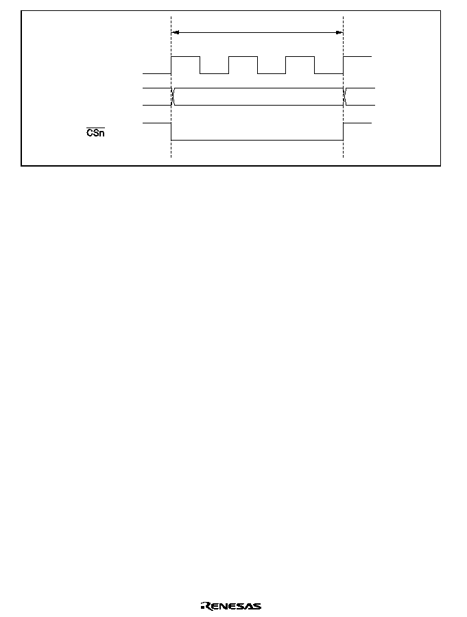
Rev. 2.0, 04/02, page 156 of 906
Bus cycle
T
1
T
2
T
3
Area n external address
Address bus
¯
Figure 6.7
$
$33 Signal Output Timing (n = 0 to 7)
6.5
Basic Bus Interface
The basic bus interface enables direct connection of ROM, SRAM, and so on.
6.5.1
Data Size and Data Alignment
Data sizes for the CPU and other internal bus masters are byte, word, and longword. The bus
controller has a data alignment function, and when accessing external address space, controls
whether the upper data bus (D15 to D8) or lower data bus (D7 to D0) is used according to the bus
specifications for the area being accessed (8-bit access space or 16-bit access space) and the data
size.
8-Bit Access Space: Figure 6.8 illustrates data alignment control for the 8-bit access space. With
the 8-bit access space, the upper data bus (D15 to D8) is always used for accesses. The amount of
data that can be accessed at one time is one byte: a word access is performed as two byte accesses,
and a longword access, as four byte accesses.
Rev. 2.0, 04/02, page 157 of 906
D15
D8 D7
D0
Upper data bus
Lower data bus
Byte size
Word size
1st bus cycle
2nd bus cycle
Longword
size
1st bus cycle
2nd bus cycle
3rd bus cycle
4th bus cycle
Figure 6.8 Access Sizes and Data Alignment Control (8-Bit Access Space)
16-Bit Access Space: Figure 6.9 illustrates data alignment control for the 16-bit access space.
With the 16-bit access space, the upper data bus (D15 to D8) and lower data bus (D7 to D0) are
used for accesses. The amount of data that can be accessed at one time is one byte or one word,
and a longword access is executed as two word accesses.
In byte access, whether the upper or lower data bus is used is determined by whether the address is
even or odd. The upper data bus is used for an even address, and the lower data bus for an odd
address.
D15
D8 D7
D0
Upper data bus
Lower data bus
Byte size
Word size
1st bus cycle
2nd bus cycle
Longword
size
∑ Even address
Byte size
∑ Odd address
Figure 6.9 Access Sizes and Data Alignment Control (16-bit Access Space)

Rev. 2.0, 04/02, page 158 of 906
6.5.2
Valid Strobes
Table 6.3 shows the data buses used and valid strobes for the access spaces.
In a read, the
5' signal is valid for both the upper and the lower half of the data bus. In a write,
the
+:5 signal is valid for the upper half of the data bus, and the /:5 signal for the lower half.
Table 6.3
Data Buses Used and Valid Strobes
Area
Access
Size
Read/
Write
Address
Valid
Strobe
Upper Data Bus
(D15 to D8)
Lower Data Bus
(D7 to D0)
8-bit access
Byte
Read
--
5'
Valid
Invalid
space
Write
--
+:5
Hi-Z
16-bit access
Byte
Read
Even
5'
Valid
Invalid
space
Odd
Invalid
Valid
Write
Even
+:5
Valid
Hi-Z
Odd
/:5
Hi-Z
Valid
Word
Read
--
5'
Valid
Valid
Write
--
+:5
,
/:5
Valid
Valid
Note: Hi-Z: High-impedance state
Invalid: Input state; input value is ignored.
6.5.3
Basic Operation Timing
8-Bit, 2-State Access Space: Figure 6.10 shows the bus timing for an 8-bit, 2-state access space.
When an 8-bit access space is accessed, the upper half (D15 to D8) of the data bus is used. The
/:5 pin is always fixed high. Wait states can be inserted.

Rev. 2.0, 04/02, page 159 of 906
Bus cycle
T
1
T
2
Address bus
¯
D15 to D8
Valid
D7 to D0
Invalid
Read
D15 to D8
Valid
D7 to D0
High impedance
Write
High
Notes: 1. n = 0 to 7
2. When RDNn = 0
Figure 6.10 Bus Timing for 8-Bit, 2-State Access Space
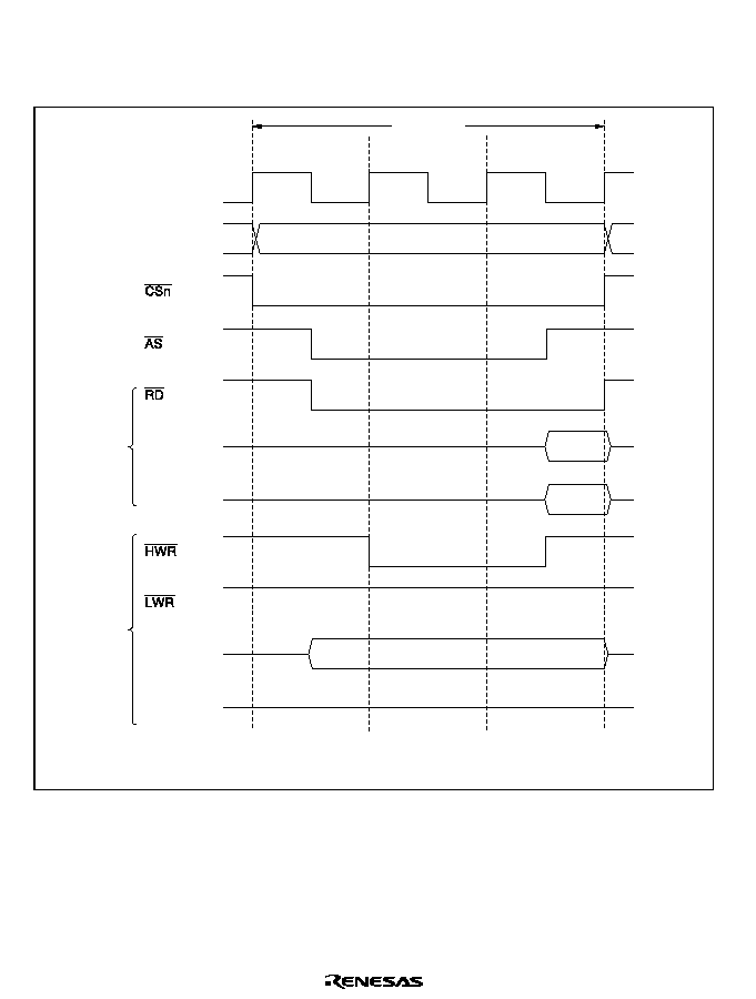
Rev. 2.0, 04/02, page 160 of 906
8-Bit, 3-State Access Space: Figure 6.11 shows the bus timing for an 8-bit, 3-state access space.
When an 8-bit access space is accessed, the upper half (D15 to D8) of the data bus is used. The
/:5 pin is always fixed high. Wait states can be inserted.
Bus cycle
T
1
T
2
Address bus
¯
D15 to D8
Valid
D7 to D0
Invalid
Read
D15 to D8
Valid
D7 to D0
Write
High
T
3
High impedance
Notes: 1. n = 0 to 7
2. When RDNn = 0
Figure 6.11 Bus Timing for 8-Bit, 3-State Access Space
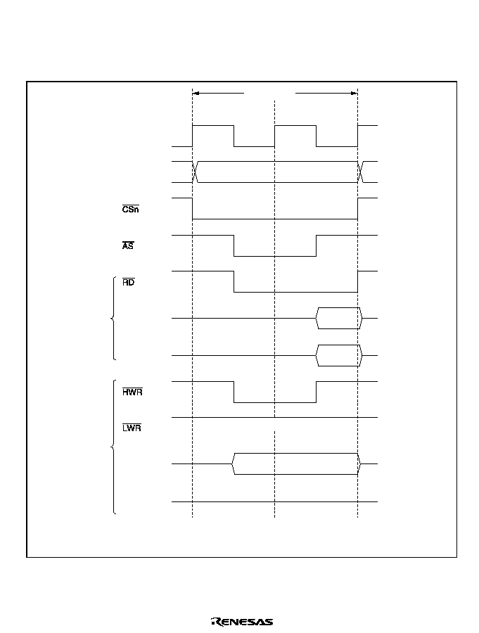
Rev. 2.0, 04/02, page 161 of 906
16-Bit, 2-State Access Space: Figures 6.12 to 6.14 show bus timings for a 16-bit, 2-state access
space. When a 16-bit access space is accessed, the upper half (D15 to D8) of the data bus is used
for odd addresses, and the lower half (D7 to D0) for even addresses. Wait states cannot be
inserted.
Bus cycle
T
1
T
2
Address bus
¯
D15 to D8
Valid
D7 to D0
Invalid
Read
D15 to D8
Valid
D7 to D0
Write
High
High impedance
Notes: 1. n = 0 to 7
2. When RDNn = 0
Figure 6.12 Bus Timing for 16-Bit, 2-State Access Space
(Even Address Byte Access)
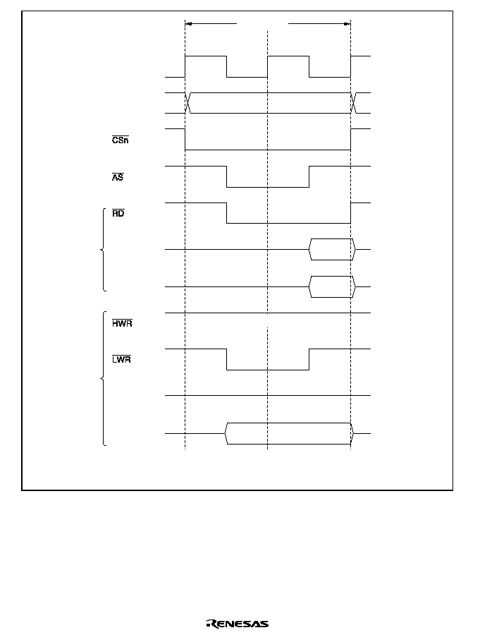
Rev. 2.0, 04/02, page 162 of 906
Bus cycle
T
1
T
2
Address bus
¯
D15 to D8
Invalid
D7 to D0
Valid
Read
D15 to D8
D7 to D0
Valid
Write
High
High impedance
Notes: 1. n = 0 to 7
2. When RDNn = 0
Figure 6.13 Bus Timing for 16-Bit, 2-State Access Space
(Odd Address Byte Access)

Rev. 2.0, 04/02, page 163 of 906
Bus cycle
T
1
T
2
Address bus
¯
D15 to D8
Valid
D7 to D0
Valid
Read
D15 to D8
Valid
D7 to D0
Valid
Write
Notes: 1. n = 0 to 7
2. When RDNn = 0
Figure 6.14 Bus Timing for 16-Bit, 2-State Access Space
(Word Access)
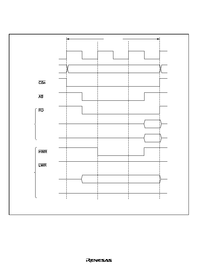
Rev. 2.0, 04/02, page 164 of 906
16-Bit, 3-State Access Space: Figures 6.15 to 6.17 show bus timings for a 16-bit, 3-state access
space. When a 16-bit access space is accessed, the upper half (D15 to D8) of the data bus is used
for the even address, and the lower half (D7 to D0) for the odd address. Wait states can be
inserted.
Bus cycle
T
1
T
2
Address bus
¯
D15 to D8
Valid
D7 to D0
Invalid
Read
D15 to D8
Valid
D7 to D0
Write
High
T
3
High impedance
Notes: 1. n = 0 to 7
2. When RDNn = 0
Figure 6.15 Bus Timing for 16-Bit, 3-State Access Space
(Even Address Byte Access)

Rev. 2.0, 04/02, page 165 of 906
Bus cycle
T
1
T
2
Address bus
¯
D15 to D8
Invalid
D7 to D0
Valid
Read
D15 to D8
D7 to D0
Valid
Write
High
T
3
High impedance
Notes: 1. n = 0 to 7
2. When RDNn = 0
Figure 6.16 Bus Timing for 16-Bit, 3-State Access Space
(Odd Address Byte Access)
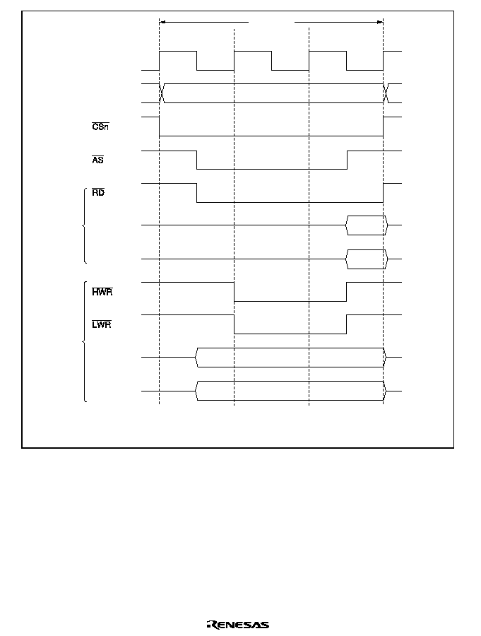
Rev. 2.0, 04/02, page 166 of 906
Bus cycle
T
1
T
2
Address bus
¯
D15 to D8
Valid
D7 to D0
Valid
Read
D15 to D8
Valid
D7 to D0
Valid
Write
T
3
Notes: 1. n = 0 to 7
2. When RDNn = 0
Figure 6.17 Bus Timing for 16-Bit, 3-State Access Space
(Word Access)
6.5.4
Wait Control
When accessing external space, this LSI can extend the bus cycle by inserting one or more wait
states (T
w
). There are two ways of inserting wait states: program wait insertion and pin wait
insertion using the
:$,7 pin.

Rev. 2.0, 04/02, page 167 of 906
Program Wait Insertion: From 0 to 7 wait states can be inserted automatically between the T
2
state and T
3
state on an individual area basis in 3-state access space, according to the settings in
WTCRA and WTCRB.
Pin Wait Insertion: Setting the WAITE bit to 1 in BCR enables wait input by means of the
:$,7 pin. When external space is accessed in this state, a program wait is first inserted in
accordance with the settings in WTCRA and WTCRB. If the
:$,7 pin is low at the falling edge
of ¯ in the last T
2
or T
w
state, another T
w
state is inserted. If the
:$,7 pin is held low, T
w
states are
inserted until it goes high. This is useful when inserting seven or more T
w
states, or when changing
the number of T
w
states to be inserted for different external devices. The WAITE bit setting applies
to all areas. Figure 6.18 shows an example of wait state insertion timing.
The settings after a reset are: 3-state access, insertion of 7 program wait states, and
:$,7 input
disabled.
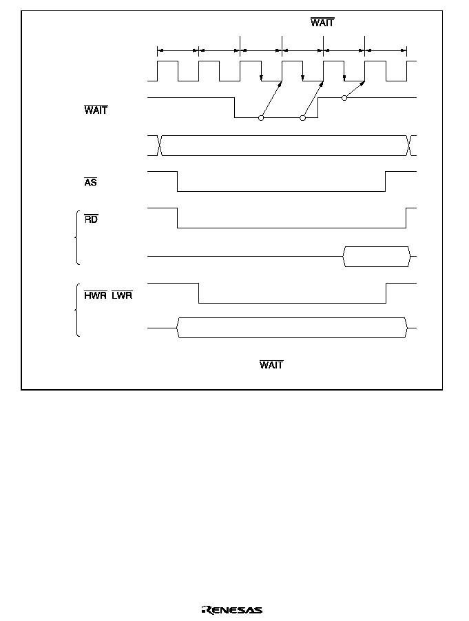
Rev. 2.0, 04/02, page 168 of 906
By program wait
T
1
Address bus
¯
Data bus
Read data
Read
,
Write data
Write
Data bus
T
2
T
w
T
w
T
w
T
3
By
pin
Notes: 1. Downward arrows indicate the timing of
pin sampling.
2. When RDN = 0
Figure 6.18 Example of Wait State Insertion Timing
6.5.5
Read Strobe (
#
#) Timing
The read strobe (
5') timing can be changed for individual areas by setting bits RDN7 to RDN0 to
1 in RDNCR. Figure 6.19 shows an example of the timing when the read strobe timing is changed
in basic bus 3-state access space.
When the DMAC or EXDMAC is used in single address mode, note that if the
5' timing is
changed by setting RDNn to 1, the
5' timing will change relative to the rise of '$&. or
('$&..
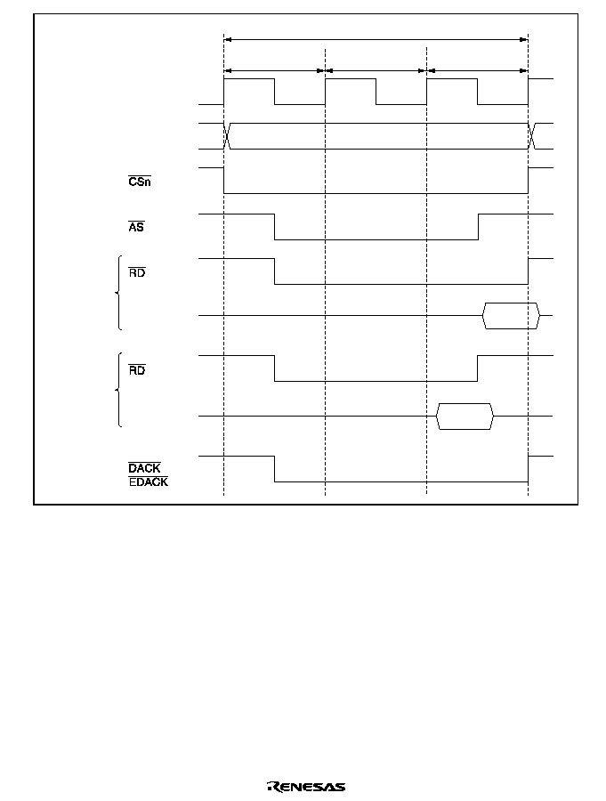
Rev. 2.0, 04/02, page 169 of 906
Bus cycle
T
1
T
2
Address bus
¯
T
3
Data bus
,
Data bus
RDNn = 0
RDNn = 1
Figure 6.19 Example of Read Strobe Timing
6.5.6
Extension of Chip Select (
$
$) Assertion Period
Some external I/O devices require a setup time and hold time between address and
&6 signals and
strobe signals such as
5', +:5, and /:5. Settings can be made in the CSACR register to insert
states in which only the
&6, $6, and address signals are asserted before and after a basic bus space
access cycle. Extension of the
&6 assertion period can be set for individual areas. With the &6
assertion extension period in write access, the data setup and hold times are less stringent since the
write data is output to the data bus.
Figure 6.20 shows an example of the timing when the
&6 assertion period is extended in basic bus
3-state access space.
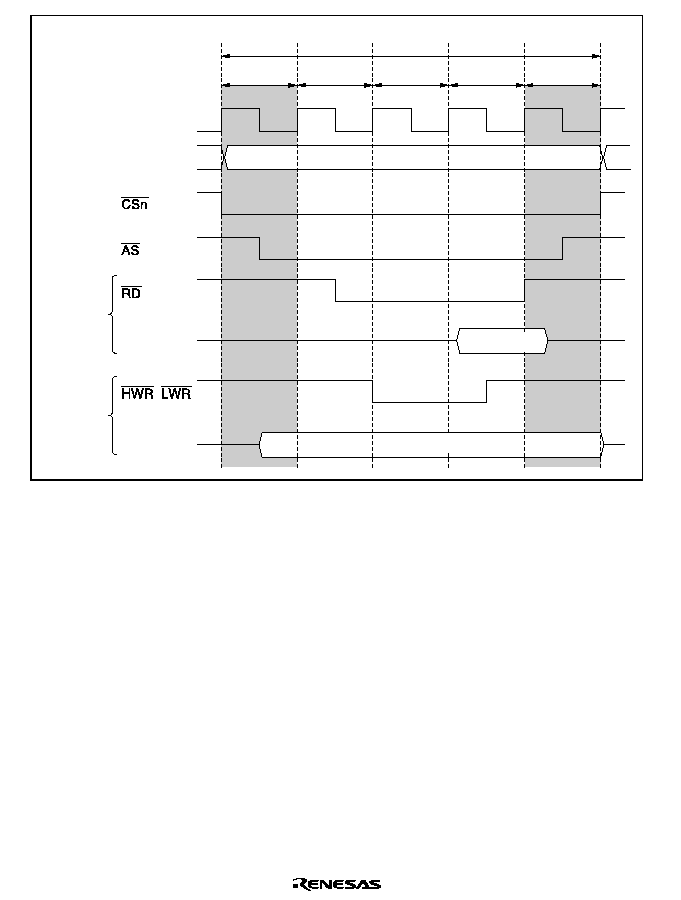
Rev. 2.0, 04/02, page 170 of 906
T
h
Address bus
¯
T
1
T
2
T
3
T
t
Bus cycle
Data bus
,
Write
Data bus
Read
(when
RDNn = 0)
Read data
Write data
Figure 6.20 Example of Timing when Chip Select Assertion Period is Extended
Both extension state T
h
inserted before the basic bus cycle and extension state T
t
inserted after the
basic bus cycle, or only one of these, can be specified for individual areas. Insertion or non-
insertion can be specified for the T
h
state with the upper 8 bits (CSXH7 to CSXH0) in the CSACR
register, and for the T
t
state with the lower 8 bits (CSXT7 to CSXT0).
6.6
DRAM Interface
In this LSI, external space areas 2 to 5 can be designated as DRAM space, and DRAM interfacing
performed. The DRAM interface allows DRAM to be directly connected to this LSI. A DRAM
space of 2, 4, or 8 Mbytes can be set by means of bits RMTS2 to RMTS0 in DRAMCR. Burst
operation is also possible, using fast page mode.
6.6.1
Setting DRAM Space
Areas 2 to 5 are designated as DRAM space by setting bits RMTS2 to RMTS0 in DRAMCR. The
relation between the settings of bits RMTS2 to RMTS0 and DRAM space is shown in table 6.4.

Rev. 2.0, 04/02, page 171 of 906
Possible DRAM space settings are: one area (area 2), two areas (areas 2 and 3), four areas (areas 2
to 5), and continuous area (areas 2 to 5).
Table 6.4
Relation between Settings of Bits RMTS2 to RMTS0 and DRAM Space
RMTS2
RMTS1
RMTS0
Area 5
Area 4
Area 3
Area 2
0
0
1
Normal space
Normal space
Normal space
DRAM space
1
0
Normal space
Normal space
DRAM space
DRAM space
1
DRAM space
DRAM space
DRAM space
DRAM space
1
0
Continuous synchronous DRAM space
*
0
1
Mode register settings of synchronous DRAM
*
1
0
Reserved (setting prohibited)
1
Continuous
DRAM space
Continuous
DRAM space
Continuous
DRAM space
Continuous
DRAM space
Note: Reserved (setting prohibited) in the H8S/2678 Series.
With continuous DRAM space,
5$6 is valid. The bus specifications (bus width, number of wait
states, etc.) for continuous DRAM space conform to the settings for area 2.
6.6.2
Address Multiplexing
With DRAM space, the row address and column address are multiplexed. In address multiplexing,
the size of the shift of the row address is selected with bits MXC2 to MXC0 in DRAMCR. Table
6.5 shows the relation between the settings of MXC2 to MXC0 and the shift size.
The MXC2 bit should be cleared to 0 when the DRAM interface is used.

Rev. 2.0, 04/02, page 172 of 906
Table 6.5
Relation between Settings of Bits MXC2 to MXC0 and Address Multiplexing
DRAMCR
Address Pins
MXC2 MXC1 MXC0 Shift Size
A23
to
A16 A15 A14 A13 A12 A11 A10 A9
A8
A7
A6
A5
A4
A3
A2
A1
A0
Row
address
0
0
0
8 bits
A23
to
A16
A23 A22 A21 A20 A19 A18 A17 A16 A15 A14 A13 A12 A11 A10 A9
A8
1
9 bits
A23
to
A16
A15 A23 A22 A21 A20 A19 A18 A17 A16 A15 A14 A13 A12 A11 A10 A9
1
0
10 bits
A23
to
A16
A15 A14 A23 A22 A21 A20 A19 A18 A17 A16 A15 A14 A13 A12 A11 A10
1
11 bits
A23
to
A16
A15 A14 A13 A23 A22 A21 A20 A19 A18 A17 A16 A15 A14 A13 A12 A11
1
x
x
Reserved (setting prohibited)
Column
address
0
*
x
x
--
A23
to
A16
A15 A14 A13 A12 A11 A10 A9
A8
A7
A6
A5
A4
A3
A2
A1
A0
1
*
x
x
Reserved (setting prohibited)
Note: In the H8S/2678 Series, address pins are A23 to A0.
x: Don't care.
6.6.3
Data Bus
If a bit in ABWCR corresponding to an area designated as DRAM space is set to 1, that area is
designated as 8-bit DRAM space; if the bit is cleared to 0, the area is designated as 16-bit DRAM
space. In 16-bit DRAM space,
◊
16-bit configuration DRAM can be connected directly.
In 8-bit DRAM space the upper half of the data bus, D15 to D8, is enabled, while in 16-bit DRAM
space both the upper and lower halves of the data bus, D15 to D0, are enabled.
Access sizes and data alignment are the same as for the basic bus interface: see section 6.5.1, Data
Size and Data Alignment.

Rev. 2.0, 04/02, page 173 of 906
6.6.4
Pins Used for DRAM Interface
Table 6.6 shows the pins used for DRAM interfacing and their functions. Since the
&6 to &6
pins are in the input state after a reset, set the corresponding DDR to 1 when
5$6 to 5$6
signals are output.
Table 6.6
DRAM Interface Pins
Pin
With DRAM
Setting
Name
I/O
Function
+:5
:(
Write enable
Output
Write enable for DRAM space
access
&6
5$6
/
5$6
Row address strobe 2/
row address strobe
Output
Row address strobe when area 2
is designated as DRAM space or
row address strobe when areas
2 to 5 are designated as
continuous DRAM space
&6
5$6
Row address strobe 3
Output
Row address strobe when area 3
is designated as DRAM space
&6
5$6
Row address strobe 4
Output
Row address strobe when area 4
is designated as DRAM space
&6
5$6
Row address strobe 5
Output
Row address strobe when area 5
is designated as DRAM space
8&$6
8&$6
Upper column address
strobe
Output
Upper column address strobe for
16-bit DRAM space access or
column address strobe for 8-bit
DRAM space access
/&$6
/&$6
Lower column address
strobe
Output
Lower column address strobe
signal for 16-bit DRAM space
access
5'
,
2(
2(
Output enable
Output
Output enable signal for DRAM
space access
:$,7
:$,7
Wait
Input
Wait request signal
A15 to A0
A15 to A0
Address pins
Output
Row address/column address
multiplexed output
D15 to D0
D15 to D0
Data pins
I/O
Data input/output pins
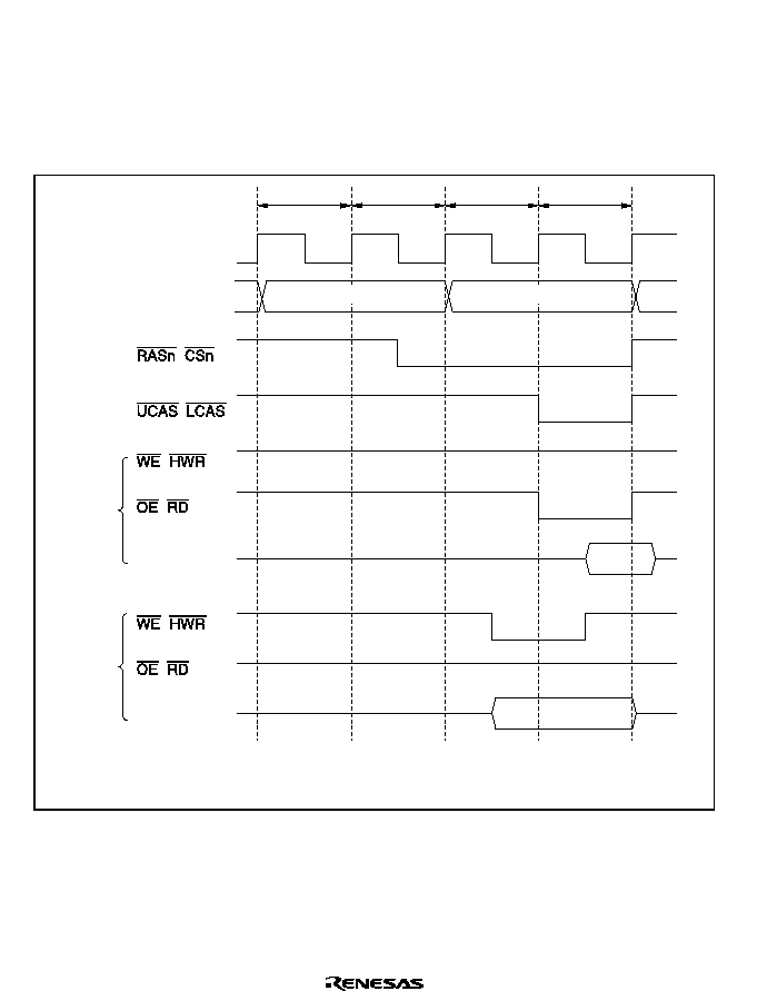
Rev. 2.0, 04/02, page 174 of 906
6.6.5
Basic Timing
Figure 6.21 shows the basic access timing for DRAM space.
The four states of the basic timing consist of one T
p
(precharge cycle) state, one T
r
(row address
output cycle) state, and the T
c1
and two T
c2
(column address output cycle) states.
T
p
¯
(
)
Read
Write
,
(
)
(
)
Data bus
(
)
(
)
Data bus
Address bus
T
r
T
c1
T
c2
Row address
High
High
Column address
Note: n = 2 to 5
Figure 6.21 DRAM Basic Access Timing (RAST = 0, CAST = 0)
When DRAM space is accessed, the
5' signal is output as the 2( signal for DRAM. When
connecting DRAM provided with an EDO page mode, the
2( signal should be connected to the
(
2( ) pin of the DRAM. Setting the OEE bit to 1 in DRAMCR enables the 2( signal for DRAM
space to be output from a dedicated
2( pin. In this case, the 2( signal for DRAM space is output
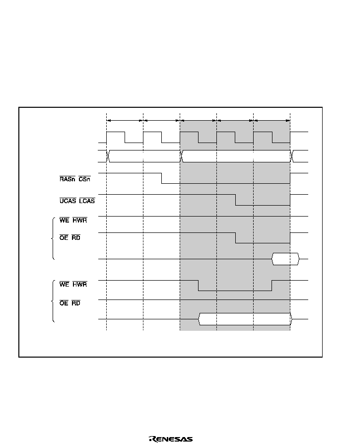
Rev. 2.0, 04/02, page 175 of 906
from both the
5' pin and the (2() pin, but in external read cycles for other than DRAM space,
the signal is output only from the
5' pin.
6.6.6
Column Address Output Cycle Control
The column address output cycle can be changed from 2 states to 3 states by setting the CAST bit
to 1 in DRAMCR. Use the setting that gives the optimum specification values (
&$6 pulse width,
etc.) according to the DRAM connected and the operating frequency of this LSI. Figure 6.22
shows an example of the timing when a 3-state column address output cycle is selected.
T
p
¯
(
)
Read
Write
,
(
)
(
)
Data bus
(
)
(
)
Data bus
Address bus
T
r
T
c1
T
c2
T
c3
Row address
Column address
High
High
Note: n = 2 to 5
Figure 6.22 Example of Access Timing with 3-State Column Address Output Cycle
(RAST = 0)
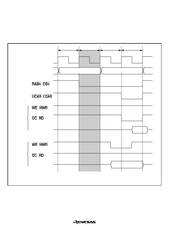
Rev. 2.0, 04/02, page 176 of 906
6.6.7
Row Address Output State Control
If the RAST bit is set to 1 in DRAMCR, the
5$6 signal goes low from the beginning of the T
r
state, and the row address hold time and DRAM read access time are changed relative to the fall of
the
5$6 signal. Use the optimum setting according to the DRAM connected and the operating
frequency of this LSI. Figure 6.23 shows an example of the timing when the
5$6 signal goes low
from the beginning of the T
r
state.
T
p
¯
(
)
Read
Write
,
(
)
(
)
Data bus
(
)
(
)
Data bus
Address bus
T
r
T
c1
T
c2
Row address
Column address
High
High
Note: n = 2 to 5
Figure 6.23 Example of Access Timing when
5$6
5$6 Signal Goes Low from Beginning
of T
r
State (CAST = 0)
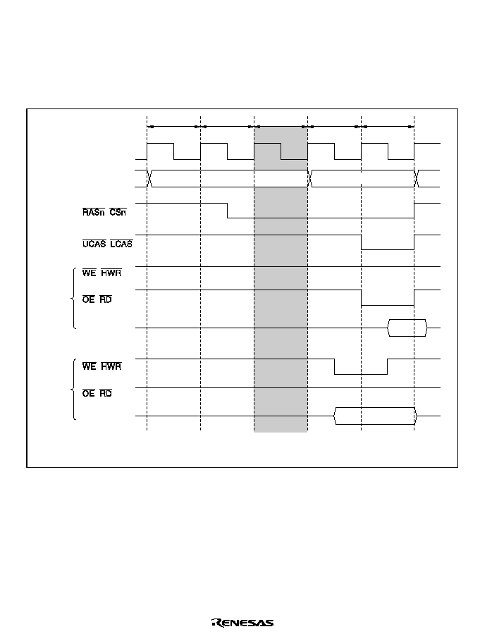
Rev. 2.0, 04/02, page 177 of 906
If a row address hold time or read access time is necessary, making a setting in bits RCD1 and
RCD0 in DRACCR allows from one to three T
rw
states, in which row address output is maintained,
to be inserted between the T
r
cycle, in which the
5$6 signal goes low, and the T
c1
cycle, in which
the column address is output. Use the setting that gives the optimum row address signal hold time
relative to the falling edge of the
5$6 signal according to the DRAM connected and the operating
frequency of this LSI. Figure 6.24 shows an example of the timing when one T
rw
state is set.
T
p
¯
(
)
Read
Write
,
(
)
(
)
Data bus
(
)
(
)
Data bus
Address bus
T
r
T
rw
T
c1
T
c2
Row address
Column address
High
High
Note: n = 2 to 5
Figure 6.24 Example of Timing with One Row Address Output Maintenance State
(RAST = 0, CAST = 0)

Rev. 2.0, 04/02, page 178 of 906
6.6.8
Precharge State Control
When DRAM is accessed, a
5$6 precharge time must be secured. With this LSI, one T
p
state is
always inserted when DRAM space is accessed. From one to four T
p
states can be selected by
setting bits TPC1 and TPC0 in DRACCR. Set the optimum number of T
p
cycles according to the
DRAM connected and the operating frequency of this LSI. Figure 6.25 shows the timing when
two T
p
states are inserted. The setting of bits TPC1 and TPC0 is also valid for T
p
states in refresh
cycles.
T
p1
¯
(
)
Read
Write
,
(
)
(
)
Data bus
(
)
(
)
Data bus
Address bus
T
p2
T
r
T
c1
T
c2
Row address
Column address
High
High
Note: n = 2 to 5
Figure 6.25 Example of Timing with Two-State Precharge Cycle
(RAST = 0, CAST = 0)

Rev. 2.0, 04/02, page 179 of 906
6.6.9
Wait Control
There are two ways of inserting wait states in a DRAM access cycle: program wait insertion and
pin wait insertion using the
:$,7 pin.
Wait states are inserted to extend the
&$6 assertion period in a read access to DRAM space, and
to extend the write data setup time relative to the falling edge of
&$6 in a write access.
Program Wait Insertion: When the bit in ASTCR corresponding to an area designated as DRAM
space is set to 1, from 0 to 7 wait states can be inserted automatically between the T
c1
state and T
c2
state, according to the settings in registers WTCRA and WTCRB.
Pin Wait Insertion: When the WAITE bit in BCR is set to 1 and the ASTCR bit is set to 1, wait
input by means of the
:$,7 pin is enabled. When DRAM space is accessed in this state, a
program wait (T
w
) is first inserted. If the
:$,7 pin is low at the falling edge of ¯ in the last T
c1
or
T
w
state, another T
w
state is inserted. If the
:$,7 pin is held low, T
w
states are inserted until it
goes high.
Figures 6.26 and 6.27 show examples of wait cycle insertion timing in the case of 2-state and 3-
state column address output cycles.
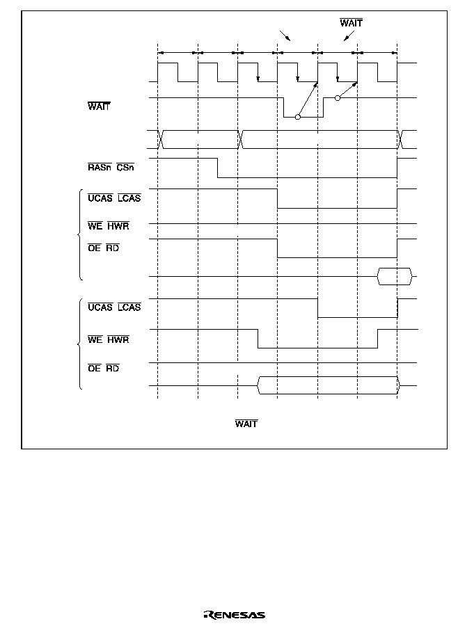
Rev. 2.0, 04/02, page 180 of 906
By program wait
T
p
Address bus
¯
T
r
T
c1
T
w
T
w
T
c2
By
pin
(
)
Read
Write
,
,
(
)
(
)
Data bus
(
)
(
)
Data bus
Row address
Column address
High
High
Note: Downward arrows indicate the timing of
pin sampling.
n = 2 to 5
Figure 6.26 Example of Wait State Insertion Timing
(2-State Column Address Output)

Rev. 2.0, 04/02, page 181 of 906
By program wait
T
p
Address bus
¯
T
r
T
c1
T
w
T
w
T
c2
T
c3
By
pin
(
)
Read
Write
,
,
(
)
(
)
Data bus
(
)
(
)
Data bus
Row address
Column address
High
High
Note: Downward arrows indicate the timing of
pin sampling.
n = 2 to 5
Figure 6.27 Example of Wait State Insertion Timing
(3-State Column Address Output)
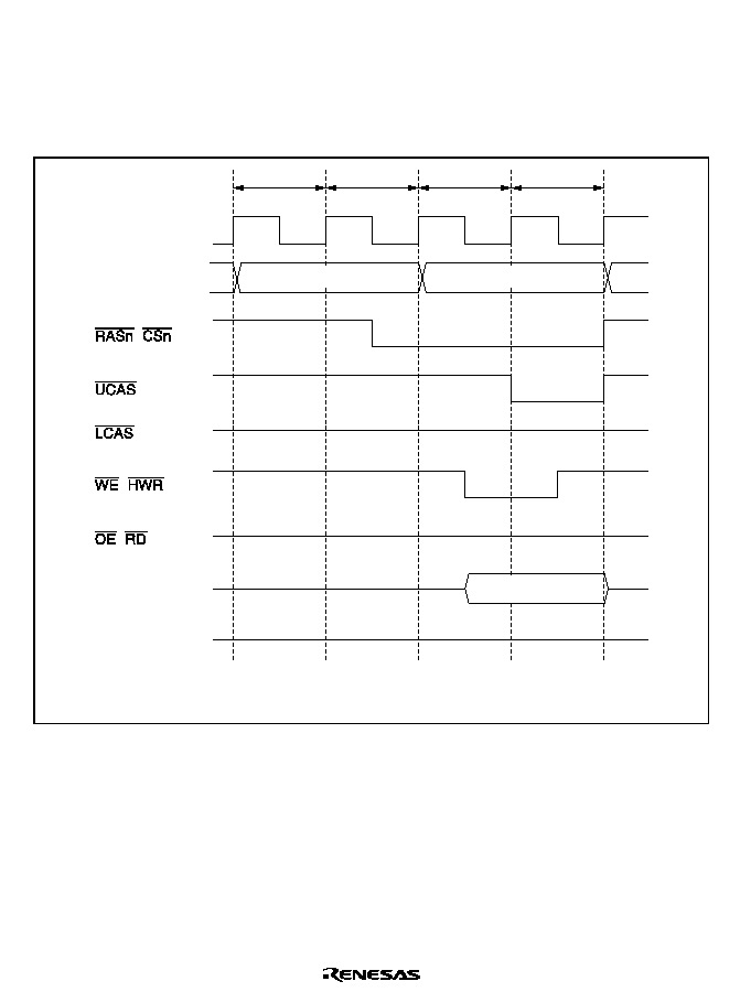
Rev. 2.0, 04/02, page 182 of 906
6.6.10
Byte Access Control
When DRAM with a
◊
16-bit configuration is connected, the 2-CAS access method is used for the
control signals needed for byte access. Figure 6.28 shows the control timing for 2-CAS access, and
figure 6.29 shows an example of 2-CAS DRAM connection.
T
p
High-Z
¯
(
)
(
)
(
)
Upper data bus
Lower data bus
Address bus
T
r
T
c1
T
c2
Note: n = 2 to 5
Row address
Column address
Write data
High
High
Figure 6.28 2-CAS Control Timing
(Upper Byte Write Access: RAST = 0, CAST = 0)
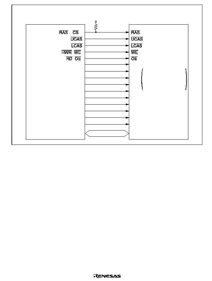
Rev. 2.0, 04/02, page 183 of 906
This LSI
(Address shift size
set to 10 bits)
n (
n)
2-CAS type 16-Mbit DRAM
1-Mbyte
◊
16-bit configuration
10-bit column address
(
)
(
)
A9
A8
A10
A9
A8
A7
A7
A6
A6
A5
A5
A4
A4
A3
A3
A2
A2
A1
A1
A0
D15 to D0
D15 to D0
Row address input:
A9 to A0
Column address input:
A9 to A0
Figure 6.29 Example of 2-CAS DRAM Connection
6.6.11
Burst Operation
With DRAM, in addition to full access (normal access) in which data is accessed by outputting a
row address for each access, a fast page mode is also provided which can be used when making
consecutive accesses to the same row address. This mode enables fast (burst) access of data by
simply changing the column address after the row address has been output. Burst access can be
selected by setting the BE bit to 1 in DRAMCR.
Burst Access (Fast Page Mode): Figures 6.30 and 6.31 show the operation timing for burst
access. When there are consecutive access cycles for DRAM space, the
&$6 signal and column
address output cycles (two states) continue as long as the row address is the same for consecutive
access cycles. The row address used for the comparison is set with bits MXC2 to MXC0 in
DRAMCR.
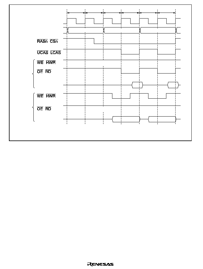
Rev. 2.0, 04/02, page 184 of 906
T
p
¯
T
r
T
c1
T
c2
T
c1
T
c2
(
)
Read
Write
,
(
)
(
)
Data bus
(
)
(
)
Data bus
Address bus
Note: n = 2 to 5
Row address
Column address 1
Column address 2
High
High
Figure 6.30 Operation Timing in Fast Page Mode
(RAST = 0, CAST = 0)
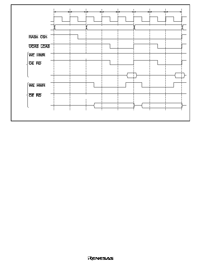
Rev. 2.0, 04/02, page 185 of 906
T
p
¯
T
r
T
c1
T
c2
T
c3
T
c1
T
c2
T
c3
(
)
Read
Write
,
(
)
(
)
Data bus
(
)
(
)
Data bus
Address bus
Note: n = 2 to 5
Row address
Column address 1
Column address 2
High
High
Figure 6.31 Operation Timing in Fast Page Mode
(RAST = 0, CAST = 1)
The bus cycle can also be extended in burst access by inserting wait states. The wait state insertion
method and timing are the same as for full access. For details see section 6.6.9, Wait Control.
RAS Down Mode and RAS Up Mode: Even when burst operation is selected, it may happen that
access to DRAM space is not continuous, but is interrupted by access to another space. In this
case, if the
5$6 signal is held low during the access to the other space, burst operation can be
resumed when the same row address in DRAM space is accessed again.
∑
RAS Down Mode
To select RAS down mode, set both the RCDM bit and the BE bit to 1 in DRAMCR. If access
to DRAM space is interrupted and another space is accessed, the
5$6 signal is held low
during the access to the other space, and burst access is performed when the row address of the
next DRAM space access is the same as the row address of the previous DRAM space access.
Figure 6.32 shows an example of the timing in RAS down mode.
Note, however, that the
5$6 signal will go high if:
a refresh operation is initiated in the RAS down state
self-refreshing is performed
the chip enters software standby mode
the external bus is released
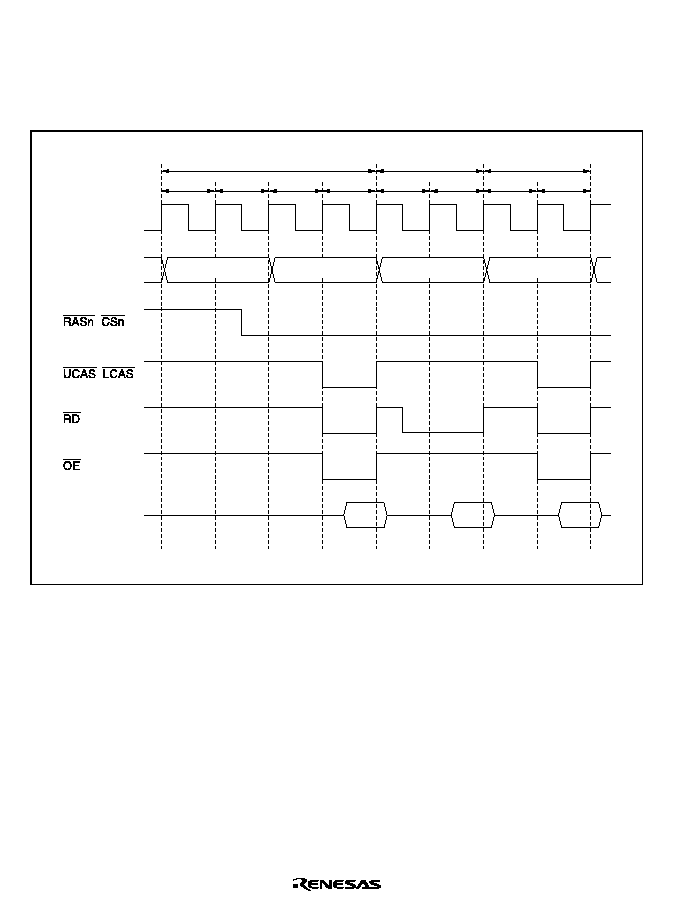
Rev. 2.0, 04/02, page 186 of 906
the RCDM bit or BE bit is cleared to 0
If a transition is made to the all-module-clocks-stopped mode in the
5$6 down state, the clock
will stop with
5$6 low. To enter the all-module-clocks-stopped mode with 5$6 high, the
RCDM bit must be cleared to 0 before executing the SLEEP instruction.
Normal space
read
DRAM space
read
T
p
T
r
T
c1
T
c2
T
1
T
2
DRAM space read
T
c1
T
c2
Note: n = 2 to 5
¯
(
)
,
Data bus
Address bus
Row address
Column address 1
Column address 2
External address
Figure 6.32 Example of Operation Timing in RAS Down Mode
(RAST = 0, CAST = 0)
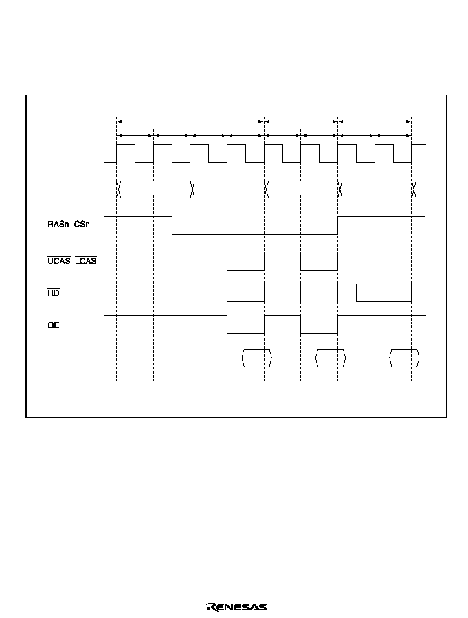
Rev. 2.0, 04/02, page 187 of 906
∑
RAS Up Mode
To select RAS up mode, clear the RCDM bit to 0 in DRAMCR. Each time access to DRAM
space is interrupted and another space is accessed, the
5$6 signal goes high again. Burst
operation is only performed if DRAM space is continuous. Figure 6.33 shows an example of
the timing in RAS up mode.
Normal space
read
DRAM space
read
T
p
T
r
T
c1
T
c2
T
c1
T
c2
DRAM space read
T
1
T
2
Note: n = 2 to 5
¯
(
)
,
Data bus
Address bus
Row address
Column address 1
Column address 2
External address
Figure 6.33 Example of Operation Timing in RAS Up Mode
(RAST = 0, CAST = 0)
6.6.12
Refresh Control
This LSI is provided with a DRAM refresh control function. CAS-before-RAS (CBR) refreshing
is used. In addition, self-refreshing can be executed when the chip enters the software standby
state.
Refresh control is enabled when any area is designated as DRAM space in accordance with the
setting of bits RMTS2 to RMTS0 in DRAMCR.
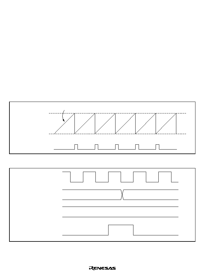
Rev. 2.0, 04/02, page 188 of 906
CAS-before-RAS (CBR) Refreshing: To select CBR refreshing, set the RFSHE bit to 1 in
REFCR.
With CBR refreshing, RTCNT counts up using the input clock selected by bits RTCK2 to RTCK0
in REFCR, and when the count matches the value set in RTCOR (compare match), refresh control
is performed. At the same time, RTCNT is reset and starts counting up again from H'00.
Refreshing is thus repeated at fixed intervals determined by RTCOR and bits RTCK2 to RTCK0.
Set a value in RTCOR and bits RTCK2 to RTCK0 that will meet the refreshing interval
specification for the DRAM used.
When bits RTCK2 to RTCK0 in REFCR are set, RTCNT starts counting up. RTCNT and RTCOR
settings should therefore be completed before setting bits RTCK2 to RTCK0. RTCNT operation is
shown in figure 6.34, compare match timing in figure 6.35, and CBR refresh timing in figure 6.36.
When the CBRM bit in REFCR is cleared to 0, access to external space other than DRAM space is
performed in parallel during the CBR refresh period.
RTCOR
H'00
Refresh request
RTCNT
Figure 6.34 RTCNT Operation
RTCNT
¯
N
RTCOR
N
H'00
Refresh request
signal and CMF bit
setting signal
Figure 6.35 Compare Match Timing
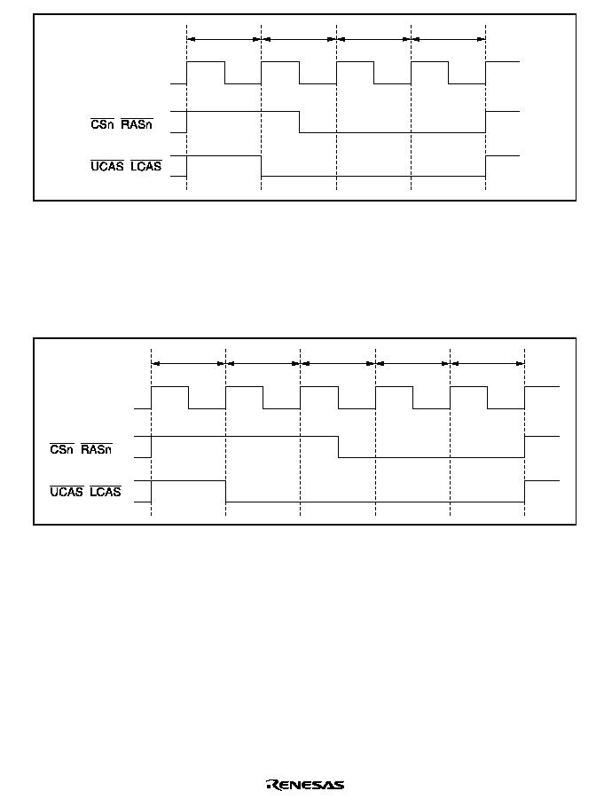
Rev. 2.0, 04/02, page 189 of 906
T
Rp
¯
(
)
T
Rr
T
Rc1
T
Rc2
,
Figure 6.36 CBR Refresh Timing
A setting can be made in bits RCW1 and RCW0 in REFCR to delay
5$6 signal output by one to
three cycles. Use bits RLW1 and RLW0 in REFCR to adjust the width of the
5$6 signal. The
settings of bits RCW1, RCW0, RLW1, and RLW0 are valid only in refresh operations.
Figure 6.37 shows the timing when bits RCW1 and RCW0 are set.
T
Rp
¯
(
)
T
Rrw
T
Rr
T
Rc1
,
T
Rc2
Figure 6.37 CBR Refresh Timing
(RCW1 = 0, RCW0 = 1, RLW1 = 0, RLW0 = 0)
Depending on the DRAM used, modification of the
:( signal may not be permitted during the
refresh period. In this case, the CBRM bit in REFCR should be set to 1. The bus controller will
then insert refresh cycles in appropriate breaks between bus cycles. Figure 6.38 shows an example
of the timing when the CBRM bit is set to 1. In this case the
&6 signal is not controlled, and
retains its value prior to the start of the refresh period.
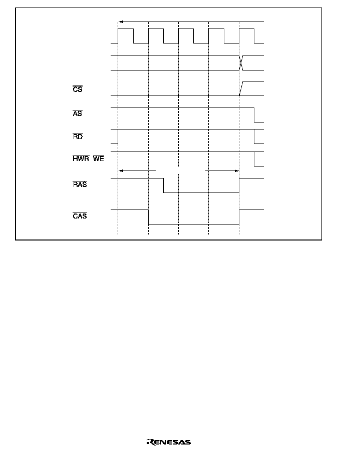
Rev. 2.0, 04/02, page 190 of 906
A23 to A0
¯
(
)
Normal space access request
Refresh period
Figure 6.38 Example of CBR Refresh Timing (CBRM = 1)
Self-Refreshing: A self-refresh mode (battery backup mode) is provided for DRAM as a kind of
standby mode. In this mode, refresh timing and refresh addresses are generated within the DRAM.
To select self-refreshing, set the RFSHE bit and SLFRF bit to 1 in REFCR. When a SLEEP
instruction is executed to enter software standby mode, the
&$6 and 5$6 signals are output and
DRAM enters self-refresh mode, as shown in figure 6.39.
When software standby mode is exited, the SLFRF bit is cleared to 0 and self-refresh mode is
exited automatically. If a CBR refresh request occurs when making a transition to software
standby mode, CBR refreshing is executed, then self-refresh mode is entered.
When using self-refresh mode, the OPE bit must not be cleared to 0 in the SBYCR register.
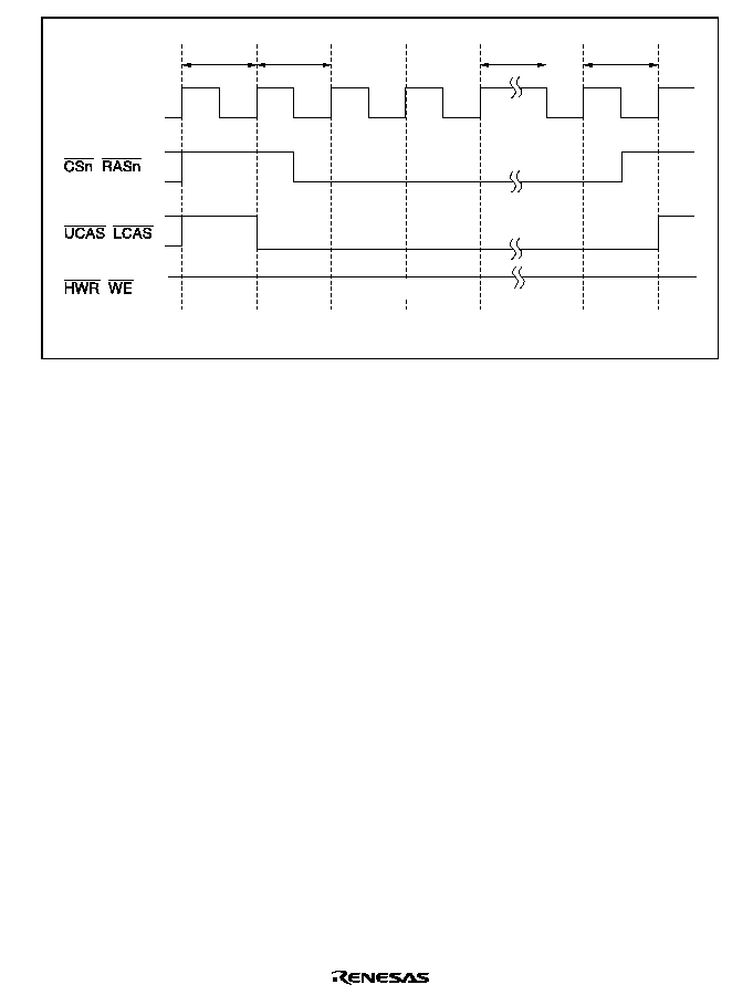
Rev. 2.0, 04/02, page 191 of 906
T
Rp
¯
T
Rr
,
Software
standby
T
Rc3
(
)
(
)
Note: n = 2 to 5
High
Figure 6.39 Self-Refresh Timing
In some DRAMs provided with a self-refresh mode, the
5$6 signal precharge time immediately
after self-refreshing is longer than the normal precharge time. A setting can be made in bits
TPCS2 to TPCS0 in REFCR to make the precharge time immediately after self-refreshing from 1
to 7 states longer than the normal precharge time. In this case, too, normal precharging is
performed according to the setting of bits TPC1 and TPC0 in DRACCR, and therefore a setting
should be made to give the optimum post-self-refresh precharge time, including this time. Figure
6.40 shows an example of the timing when the precharge time immediately after self-refreshing is
extended by 2 states.
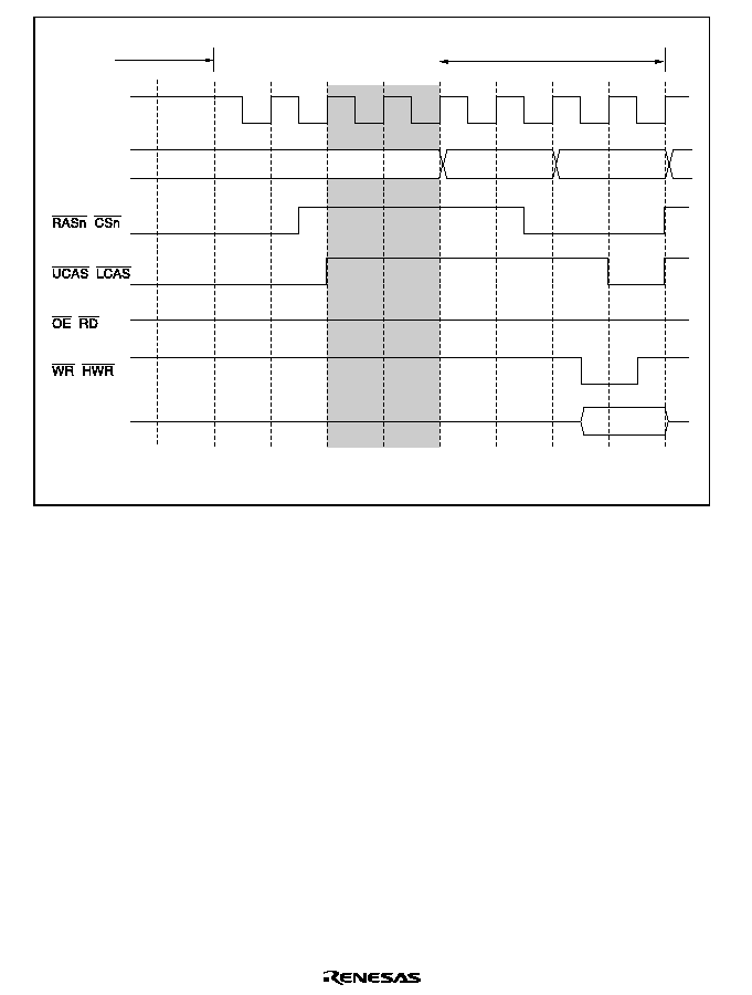
Rev. 2.0, 04/02, page 192 of 906
DRAM space write
T
rc3
T
rp1
T
rp2
T
p
T
r
Software
standby
T
c1
T
c2
Note: n = 2 to 5
¯
(
)
,
(
)
(
)
Data bus
Address bus
Figure 6.40 Example of Timing when Precharge Time after Self-Refreshing Is Extended
by 2 States
Refreshing and All-Module-Clocks-Stopped Mode: In this LSI, if the ACSE bit is set to 1 in
MSTPCRH, and then a SLEEP instruction is executed with the setting for all peripheral module
clocks to be stopped (MSTPCR = H'FFFF) or for operation of the 8-bit timer module alone
(MSTPCR = H'FFFE), and a transition is made to the sleep state, the all-module-clocks-stopped
mode is entered, in which the bus controller and I/O port clocks are also stopped. As the bus
controller clock is also stopped in this mode, CBR refreshing is not executed. If DRAM is
connected externally and DRAM data is to be retained in sleep mode, the ACSE bit must be
cleared to 0 in MSTPCRH.
6.6.13
DMAC and EXDMAC Single Address Transfer Mode and DRAM Interface
When burst mode is selected on the DRAM interface, the
'$&. and ('$&. output timing can
be selected with the DDS and EDDS bits in DRAMCR. When DRAM space is accessed in DMAC
or EXDMAC single address mode at the same time, these bits select whether or not burst access is
to be performed.

Rev. 2.0, 04/02, page 193 of 906
When DDS = 1 or EDDS = 1: Burst access is performed by determining the address only,
irrespective of the bus master. With the DRAM interface, the
'$&. or ('$&. output goes low
from the T
c1
state.
Figure 6.41 shows the
'$&. or ('$&. output timing for the DRAM interface when DDS = 1 or
EDDS = 1.
T
p
¯
(
)
Read
Write
,
(
)
(
)
Data bus
(
)
(
)
Data bus
or
Address bus
T
r
T
c1
T
c2
Note: n = 2 to 5
Row address
Column address
High
High
Figure 6.41 Example of
'$&
'$&.
./('$&.
('$&. Output Timing when DDS = 1 or EDDS = 1
(RAST = 0, CAST = 0)
When DDS = 0 or EDDS = 0: When DRAM space is accessed in DMAC or EXDMAC single
address transfer mode, full access (normal access) is always performed. With the DRAM interface,
the
'$&. or ('$&. output goes low from the T
r
state.
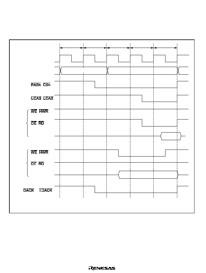
Rev. 2.0, 04/02, page 194 of 906
In modes other than DMAC or EXDMAC single address transfer mode, burst access can be used
when accessing DRAM space.
Figure 6.42 shows the
'$&. or ('$&. output timing for the DRAM interface when DDS = 0 or
EDDS = 0.
T
p
¯
(
)
Read
Write
,
(
)
(
)
Data bus
(
)
(
)
Data bus
or
Address bus
T
r
T
c1
T
c2
Note: n = 2 to 5
T
c3
Row address
Column address
High
High
Figure 6.42 Example of
'$&
'$&.
./('$&.
('$&. Output Timing when DDS = 0 or EDDS = 0
(RAST = 0, CAST = 1)

Rev. 2.0, 04/02, page 195 of 906
6.7
Synchronous DRAM Interface
In the H8S/2678R Series, external address space areas 2 to 5 can be designated as continuous
synchronous DRAM space, and synchronous DRAM interfacing performed. The synchronous
DRAM interface allows synchronous DRAM to be directly connected to this LSI. A synchronous
DRAM space of up to 8 Mbytes can be set by means of bits RMTS2 to RMTS0 in DRAMCR.
Synchronous DRAM of CAS latency 1 to 4 can be connected.
Note:
The synchronous DRAM interface is not supported in the H8S/2678 Series.
6.7.1
Setting Continuous Synchronous DRAM Space
Areas 2 to 5 are designated as continuous synchronous DRAM space by setting bits RMTS2 to
RMTS0 in DRAMCR. The relation between the settings of bits RMTS2 to RMTS0 and
synchronous DRAM space is shown in table 6.7. Possible synchronous DRAM interface settings
are and continuous area (areas 2 to 5).
Table 6.7
Relation between Settings of Bits RMTS2 to RMTS0 and Synchronous DRAM
Space
RMTS2
RMTS1
RMTS0
Area 5
Area 4
Area 3
Area 2
0
0
1
Normal space
Normal space
Normal space
DRAM space
1
0
Normal space
Normal space
DRAM space
DRAM space
1
DRAM space
DRAM space
DRAM space
DRAM space
1
0
Continuous synchronous DRAM space
*
0
1
Mode settings of synchronous DRAM
1
0
Reserved (setting prohibited)
1
Continuous DRAM space
With continuous synchronous DRAM space,
&6, &6, &6 pins are used as 5$6, &$6, :(
signal. The (
2() pin of the synchronous DRAM is used as the CKE signal, and the &6 pin is
used as synchronous DRAM clock (SDRAM
). The bus specifications for continuous
synchronous DRAM space conform to the settings for area 2. The pin wait and program wait for
the continuous synchronous DRAM are invalid.
Commands for the synchronous DRAM can be specified by combining
5$6, &$6, :(, and
address-precharge-setting command (Prechrge-sel) output on the upper column addresses.
Commands that are supported by this LSI are NOP, auto-refresh (REF), self-refresh (SELF), all
bank precharge (PALL), row address strobe bank-active (ACTV), read (READ), write (WRIT),
and mode-register write (MRS). Commands for bank control cannot be used.

Rev. 2.0, 04/02, page 196 of 906
6.7.2
Address Multiplexing
With continuous synchronous DRAM space, the row address and column address are multiplexed.
In address multiplexing, the size of the shift of the row address is selected with bits MXC2 to
MXC0 in DRAMCR. The address-precharge-setting command (Prechrge-sel) can be output on the
upper column address. Table 6.8 shows the relation between the settings of MXC2 to MXC0 and
the shift size. The MXC2 bit should be set to 1 when the synchronous DRAM interface is used.
Table 6.8
Relation between Settings of Bits MXC2 to MXC0 and Address Multiplexing
DRAMCR
Address Pins
MXC2 MXC1 MXC0
Shift
Size
A23 to
A16
A15 A14 A13 A12 A11 A10 A9
A8
A7
A6
A5
A4
A3
A2
A1
A0
Row
address
0
x
x
Reserved (setting prohibited)
1
0
0
8 bits
A23 to
A16
A23 A22 A21 A20 A19 A18 A17 A16 A15 A14 A13 A12 A11 A10 A9
A8
1
9 bits
A23 to
A16
A15 A23 A22 A21 A20 A19 A18 A17 A16 A15 A14 A13 A12 A11 A10 A9
1
0
10 bits A23 to
A16
A15 A14 A23 A22 A21 A20 A19 A18 A17 A16 A15 A14 A13 A12 A11 A10
1
11 bits A23 to
A16
A15 A14 A13 A23 A22 A21 A20 A19 A18 A17 A16 A15 A14 A13 A12 A11
Column
address
0
x
x
Reserved (setting prohibited)
1
0
0
--
A23 to
A16
P
P
P
P
P
P
P
A8
A7
A6
A5
A4
A3
A2
A1
A0
1
--
A23 to
A16
P
P
P
P
P
P
A9
A8
A7
A6
A5
A4
A3
A2
A1
A0
1
0
--
A23 to
A16
P
P
P
P
P
A10 A9
A8
A7
A6
A5
A4
A3
A2
A1
A0
1
--
A23 to
A16
P
P
P
P
A11 A10 A9
A8
A7
A6
A5
A4
A3
A2
A1
A0
X: Don't care.
P: Precharge-sel

Rev. 2.0, 04/02, page 197 of 906
6.7.3
Data Bus
If the ABW2 bit in ABWCR corresponding to an area designated as continuous synchronous
DRAM space is set to 1, area 2 to 5 are designated as 8-bit continuous synchronous DRAM space;
if the bit is cleared to 0, the areas are designated as 16-bit continuous synchronous DRAM space.
In 16-bit continuous synchronous DRAM space,
◊
16-bit configuration synchronous DRAM can be
connected directly.
In 8-bit continuous synchronous DRAM space the upper half of the data bus, D15 to D8, is
enabled, while in 16-bit continuous synchronous DRAM space both the upper and lower halves of
the data bus, D15 to D0, are enabled.
Access sizes and data alignment are the same as for the basic bus interface: see section 6.5.1, Data
Size and Data Alignment.
6.7.4
Pins Used for Synchronous DRAM Interface
Table 6.9 shows pins used for the synchronous DRAM interface and their functions. To enable the
synchronous DRAM interface, fix the DCTL pin to 1. Do not vary the DCTL pin during operation.
Since the
&6 to &6 pins are in the input state after a reset, set DDR to 1 when 5$6, &$6, and
:( signals are output. For details, see section 10, I/O Ports. Set the OEE bit of the DRAMCR
register to 1 when the CKE signal is output.

Rev. 2.0, 04/02, page 198 of 906
Table 6.9
Synchronous DRAM Interface Pins
Pin
With
Synchronous
DRAM Setting
Name
I/O
Function
&6
5$6
Row address strobe
Output
Row address strobe when
areas 2 to 5 are designated
as continuous synchronous
DRAM space
&6
&$6
Column address strobe
Output
Column address strobe when
areas 2 to 5 are designated
as continuous synchronous
DRAM space
&6
:(
Write enable
Output
Write enable strobe when
areas 2 to 5 are designated
as continuous synchronous
DRAM space
&6
SDRAM
Clock
Output
Clock only for synchronous
DRAM
(
2(
)
(CKE)
Clock enable
Output
Clock enable signal when
areas 2 to 5 are designated
as continuous synchronous
DRAM space
8&$6
DQMU
Upper data mask enable Output
Upper data mask enable for
16-bit continuous
synchronous DRAM space
access/data mask enable for
8-bit continuous synchronous
DRAM space access
/&$6
DQML
Lower data mask enable Output
Lower data mask enable
signal for 16-bit continuous
synchronous DRAM space
access
A15 to A0
A15 to A0
Address pins
Output
Row address/column address
multiplexed output pins
D15 to D0
D15 to D0
Data pins
I/O
Data input/output pins
DCTL
DCTL
Device control pin
Input
Output enable pin for
SDRAM
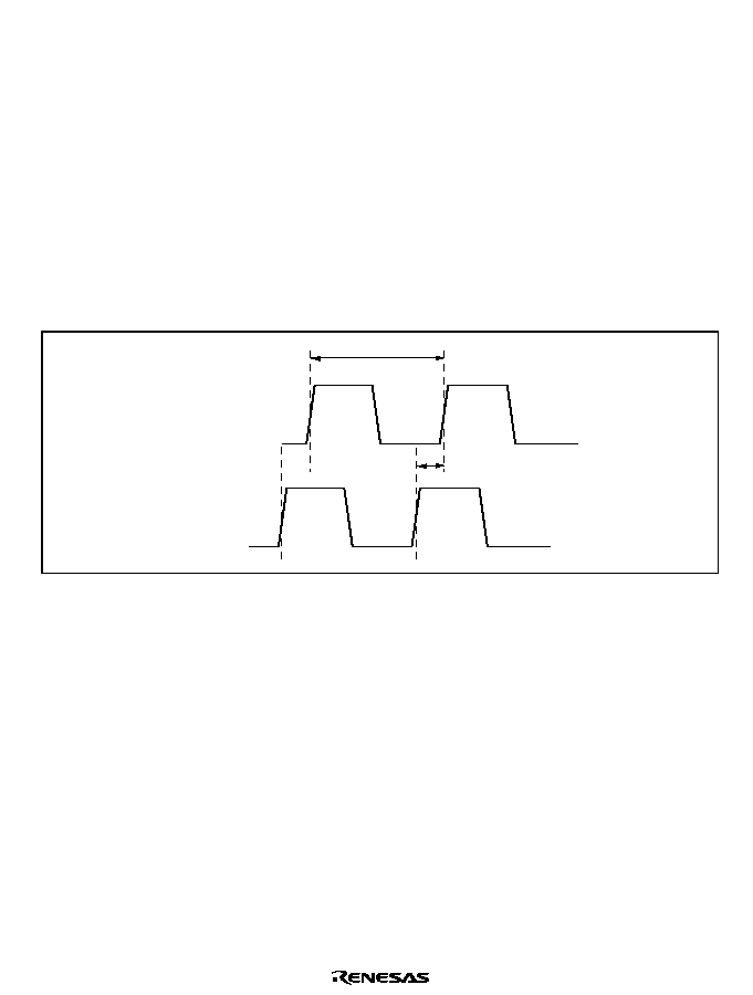
Rev. 2.0, 04/02, page 199 of 906
6.7.5
Synchronous DRAM Clock
When the DCTL pin is fixed to 1, synchronous clock (SDRAM
) is output from the
&6 pin.
When the frequency multiplication factor of the PLL circuit of this LSI is set to
◊
1 or
◊
2,
SDRAM
is 90∞ phase shift from
. Therefore, a stable margin is ensured for the synchronous
DRAM that operates at the rising edge of clocks. Figure 6.43 shows the relationship between
and SDRAM
. When the frequency multiplication factor of the PLL circuit is
◊
4, the phase of
SDRAM
and that of
are the same.
When the CLK pin of the synchronous DRAM is directly connected to SDRAM
of this LSI, it is
recommended to set the frequency multiplication factor of the PLL circuit to
◊
1 or
◊
2.
Note:
SDRAM
output timing is shown when the frequency multiplication factor of the PLL
circuit is
◊
1 or
◊
2.
SDRAM¯
Tcyc
1/4 Tcyc (90∞)
¯
Figure 6.43 Relationship between
and SDRAM
(when PLL frequency multiplication
factor is
◊
1 or
◊
2)
6.7.6
Basic Operation Timing
The four states of the basic timing consist of one T
p
(precharge cycle) state, one T
r
(row address
output cycle) state, and the T
c1
and two T
c2
(column address output cycle) states.
When areas 2 to 5 are set for the continuous synchronous DRAM space, settings of the WAITE bit
of BCR, RAST, CAST, RCDM bits of DRAMCR, and the CBRM bit of REFCR are ignored.
Figure 6.44 shows the basic timing for synchronous DRAM.

Rev. 2.0, 04/02, page 200 of 906
T
p
¯
SDRAM¯
Read
CKE
PALL
ACTV
READ
NOP
DQMU, DQML
Data bus
Address bus
T
r
T
c1
T
c2
Row address
Column address
Column address
Precharge-sel
Row address
High
Write
CKE
PALL
ACTV
NOP
WRIT
DQMU, DQML
Data bus
High
Figure 6.44 Basic Access Timing of Synchronous DRAM (CAS Latency 1)

Rev. 2.0, 04/02, page 201 of 906
6.7.7
CAS Latency Control
CAS latency is controlled by settings of the W22 to W20 bits of WTCRB. Set the CAS latency
count, as shown in table 6.10, by the setting of synchronous DRAM. Depending on the setting, the
CAS latency control cycle (T
c1
) is inserted. WTCRB can be set regardless of the setting of the
AST2 bit of ASTCR. Figure 6.45 shows the CAS latency control timing when synchronous
DRAM of CAS latency 3 is connected.
The initial value of W22 to W20 is H'7. Set the register according to the CAS latency of
synchronous DRAM to be connected.
Table 6.10
Setting CAS Latency
W22
W21
W20
Description
CAS Latency Control Cycle
Inserted
0
0
0
Connect synchronous DRAM of
CAS latency 1
0 state
1
Connect synchronous DRAM of
CAS latency 2
1 state
1
0
Connect synchronous DRAM of
CAS latency 3
2 states
1
Connect synchronous DRAM of
CAS latency 4
3 states
1
0
0
Reserved (must not used)
--
1
Reserved (must not used)
--
1
0
Reserved (must not used)
--
1
Reserved (must not used)
--
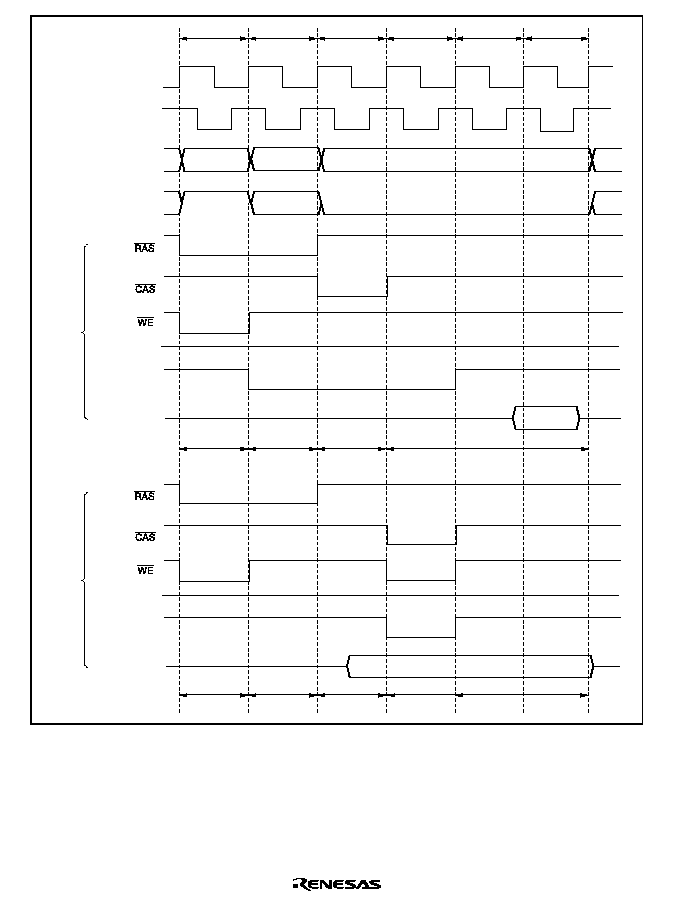
Rev. 2.0, 04/02, page 202 of 906
T
p
¯
SDRAM¯
Read
CKE
PALL
ACTV
READ
NOP
DQMU, DQML
Data bus
Address bus
T
r
T
c1
T
cl1
T
cl2
T
c2
Row address
Column address
Column address
Precharge-sel
Row address
High
Write
CKE
PALL
ACTV
NOP
NOP
WRIT
DQMU, DQML
Data bus
High
Figure 6.45 CAS Latency Control Timing (SDWCD = 0, CAS Latency 3)

Rev. 2.0, 04/02, page 203 of 906
6.7.8
Row Address Output State Control
When the command interval specification from the ACTV command to the next READ/WRIT
command cannot be satisfied, 1 to 3 states (Trw) that output the NOP command can be inserted
between the Tr cycle that outputs the ACTV command and the Tc1 cycle that outputs the column
address by setting the RCD1 and RCD0 bits of DRACCR. Use the optimum setting for the wait
time according to the synchronous DRAM connected and the operating frequency of this LSI.
Figure 6.46 shows an example of the timing when the one Trw state is set.
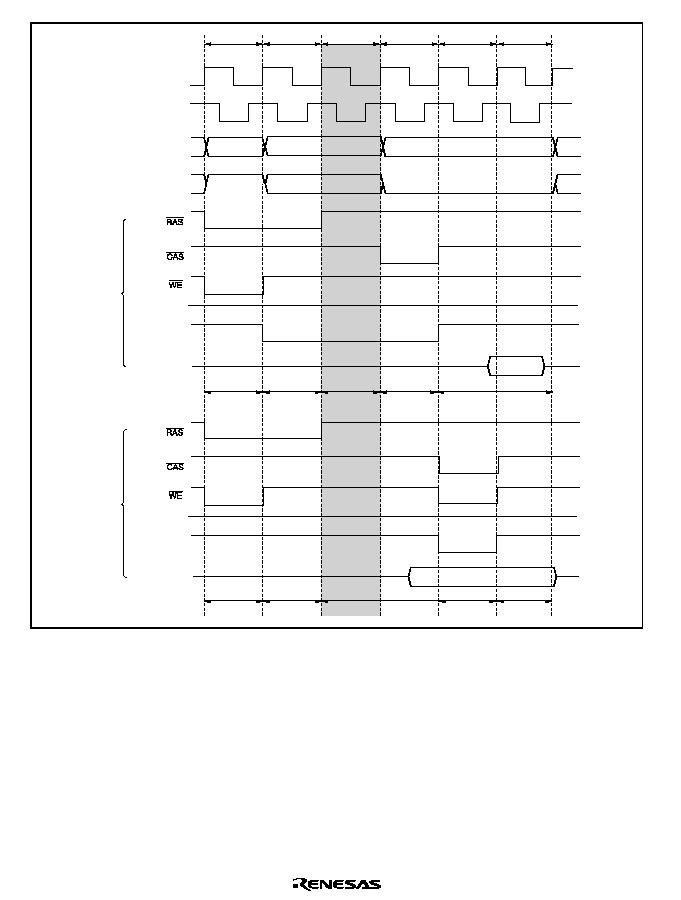
Rev. 2.0, 04/02, page 204 of 906
T
p
¯
SDRAM
¯
Read
CKE
PALL
ACTV
NOP
READ
NOP
DQMU, DQML
Data bus
Address bus
T
r
T
rw
T
c1
T
cl
T
c2
Row address
Column
address
Column address
Precharge-sel
Row address
High
Write
CKE
PALL
ACTV
NOP
NOP
WRIT
DQMU, DQML
Data bus
High
Figure 6.46 Example of Access Timing when Row Address Output Hold State is 1 State
(RCD1 = 0, RCD0 = 1, SDWCD = 0, CAS Latency 2)

Rev. 2.0, 04/02, page 205 of 906
6.7.9
Precharge State Count
When the interval specification from the PALL command to the next ACTV/REF command
cannot be satisfied, from one to four T
p
states can be selected by setting bits TPC1 and TPC0 in
DRACCR. Set the optimum number of T
p
cycles according to the synchronous DRAM connected
and the operating frequency of this LSI. Figure 6.47 shows the timing when two Tp states are
inserted.
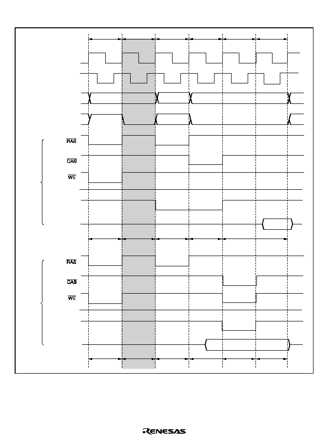
Rev. 2.0, 04/02, page 206 of 906
The setting of bits TPC1 and TPC0 is also valid for T
p
states in refresh cycles.
T
p1
¯
SDRAM
¯
Read
CKE
PALL
NOP
ACTV
READ
NOP
DQMU, DQML
Data bus
Address bus
T
p2
T
r
T
c1
T
cl
T
c2
Row address
Column address
Column address
Precharge-sel
Row address
High
Write
CKE
PALL
NOP
NOP
ACTV
NOP
WRIT
DQMU, DQML
Data bus
High
Figure 6.47 Example of Timing with Two-State Precharge Cycle
(TPC1 = 0, TPC0 = 1, SDWCD = 0, CAS Latency 2)
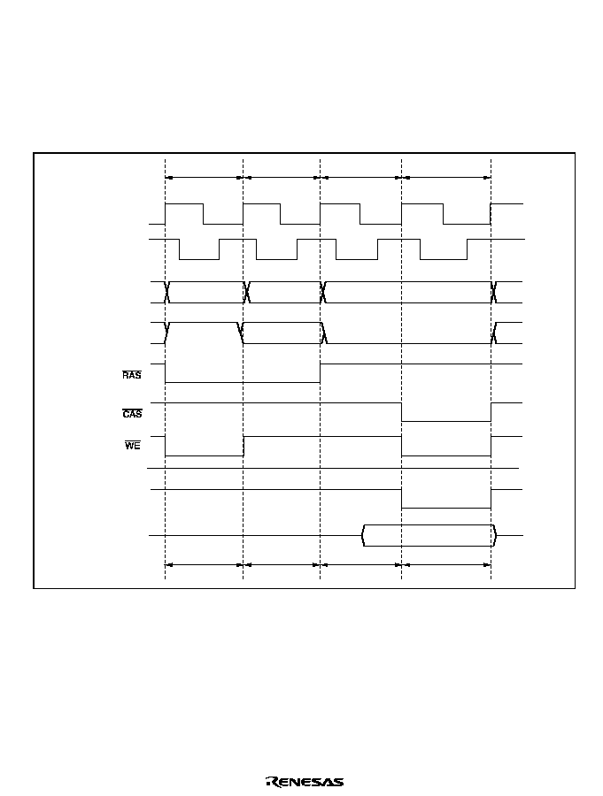
Rev. 2.0, 04/02, page 207 of 906
6.7.10
Bus Cycle Control in Write Cycle
By setting the SDWCD bit of the DRACCR to 1, the CAS latency control cycle (Tc1) that is
inserted by the WTCRB register in the write access of the synchronous DRAM can be disabled.
Disabling the CAS latency control cycle can reduce the write-access cycle count as compared to
synchronous DRAM read access. Figure 6.48 shows the write access timing when the CAS latency
control cycle is disabled.
T
p
¯
SDRAM¯
CKE
PALL
ACTV
WRIT
NOP
DQMU, DQML
Data bus
Address bus
T
r
T
c1
T
c2
Row address
Column address
Column address
Precharge-sel
Row address
High
Figure 6.48 Example of Write Access Timing when CAS Latency Control Cycle is Disabled
(SDWCD = 1)
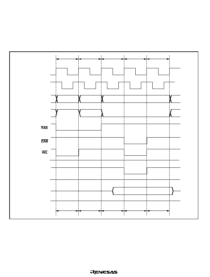
Rev. 2.0, 04/02, page 208 of 906
6.7.11
Byte Access Control
When synchronous DRAM with a
◊
16-bit configuration is connected, DQMU and DQML are
used for the control signals needed for byte access.
Figures 6.49 and 6.50 show the control timing for DQM, and figure 6.51 shows an example of
connection of byte control by DQMU and DQML.
T
p
¯
SDRAM¯
CKE
PALL
ACTV
NOP
NOP
WRIT
DQMU
DQML
Lower data bus
Upper data bus
Address bus
T
r
T
c1
T
cl
T
c2
Row address
Column address
Column address
Precharge-sel
Row address
High
High
High-Z
Figure 6.49 DQMU and DQML Control Timing
(Upper Byte Write Access: SDWCD = 0, CAS Latency 2)
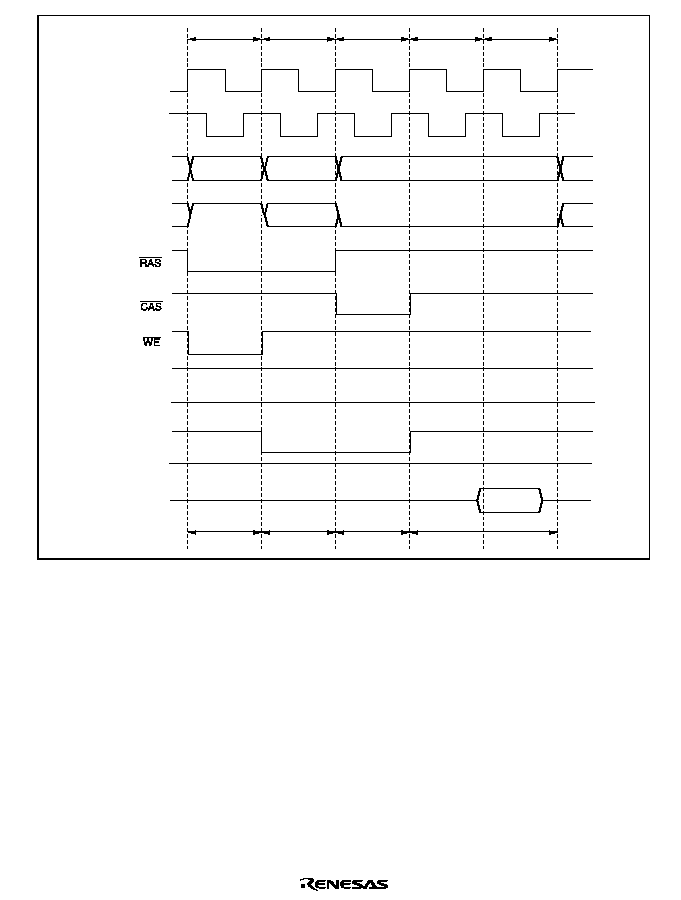
Rev. 2.0, 04/02, page 209 of 906
T
p
¯
SDRAM¯
CKE
PALL
ACTV
READ
NOP
DQMU
DQML
Lower data bus
Upper data bus
Address bus
T
r
T
c1
T
cl
T
c2
Row address
Column address
Column address
Precharge-sel
Row address
High
High
High-Z
Figure 6.50 DQMU and DQML Control Timing
(Lower Byte Read Access: CAS Latency 2)
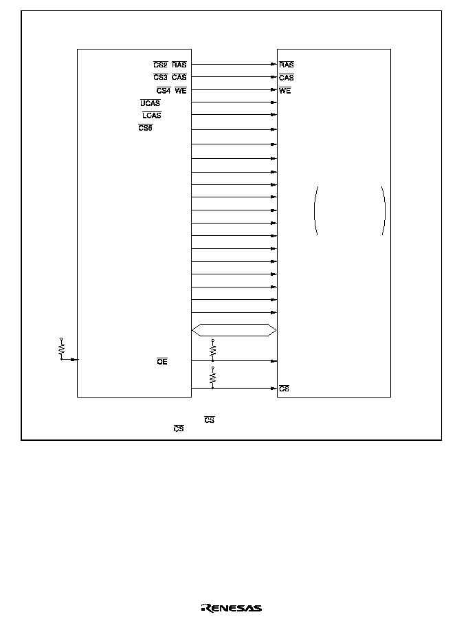
Rev. 2.0, 04/02, page 210 of 906
This LSI
(Address shift size set to 8 bits)
(
)
(
)
(
)
16-Mbit synchronous DRAM
1 Mword ◊ 16 bits ◊ 4-bank configuration
8-bit column address
(DQMU)
(DQML)
A9
A8
A10
A9
A8
A7
A12
A11
Notes: 1. Bank control is not available.
2. The CKE and
pins must be fixed to 1 when the power supply is input.
3. The
pin must be fixed to 0 before accessing synchronous DRAM.
A21
A12 (BS0)
A23
A13 (BS1)
(SDRAM¯)
CLK
DQML
DQMU
A11
A10
A7
A6
A6
A5
A5
A4
A4
A3
A3
A2
A2
A1
A1
DCTL
I/O PORT
A0
D15 to D0
DQ15 to DQ0
(CKE)
CKE
Row address
input: A11 to A0
Column address
input: A7 to A0
Bank select
address: A13/A12
Figure 6.51 Example of DQMU and DQML Byte Control
6.7.12
Burst Operation
With synchronous DRAM, in addition to full access (normal access) in which data is accessed by
outputting a row address for each access, burst access is also provided which can be used when
making consecutive accesses to the same row address. This access enables fast access of data by
simply changing the column address after the row address has been output. Burst access can be
selected by setting the BE bit to 1 in DRAMCR.

Rev. 2.0, 04/02, page 211 of 906
DQM has the 2-cycle latency when synchronous DRAM is read. Therefore, the DQM signal
cannot be specified to the Tc2 cycle data output if Tc1 cycle is performed for second or following
column address when the CAS latency is set to 1 to issue the READ command. Do not set the BE
bit to 1 when synchronous DRAM of CAS latency 1 is connected.
Burst Access Operation Timing: Figure 6.52 shows the operation timing for burst access. When
there are consecutive access cycles for continuous synchronous DRAM space, the column address
output cycles continue as long as the row address is the same for consecutive access cycles. The
row address used for the comparison is set with bits MXC2 to MXC0 in DRAMCR.
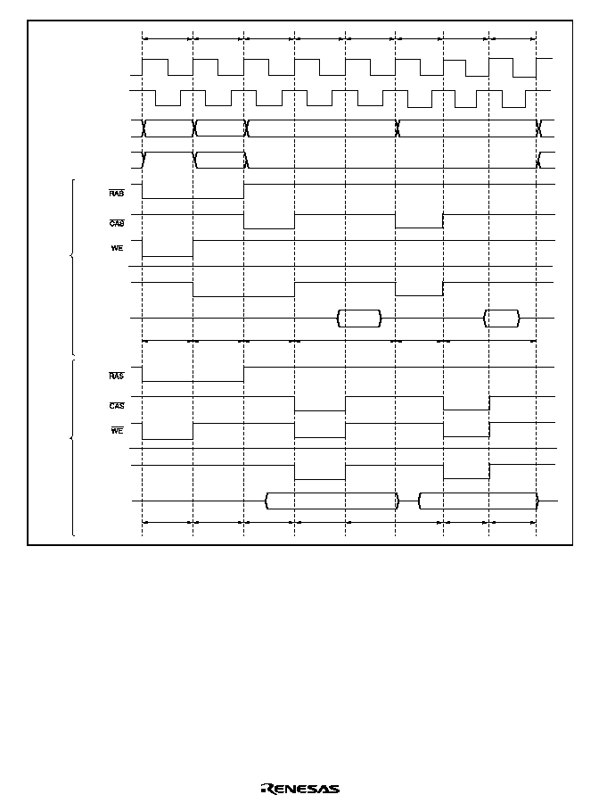
Rev. 2.0, 04/02, page 212 of 906
T
p
¯
SDRAM
¯
Read
CKE
PALL
ACTV
READ
READ
NOP
NOP
DQMU, DQML
Data bus
Address bus
T
r
T
c1
T
cl
T
c2
T
c1
T
cl
T
c2
Row address
Column
address 1
Column address
Column address 2
Precharge-sel
Row address
High
Write
CKE
PALL
ACTV
NOP
NOP
NOP
WRIT
WRIT
DQMU, DQML
Data bus
High
Figure 6.52 Operation Timing of Burst Access
(BE = 1, SDWCD = 0, CAS Latency 2)
RAS Down Mode: Even when burst operation is selected, it may happen that access to continuous
synchronous DRAM space is not continuous, but is interrupted by access to another space. In this
case, if the row address active state is held during the access to the other space, the read or write
command can be issued without ACTV command generation similarly to DRAM RAS down
mode.
To select RAS down mode, set the BE bit to 1 in DRAMCR regardless of the RCDM bit settings.
The operation corresponding to DRAM RAS up mode is not supported by this LSI.
Figure 6.53 shows an example of the timing in RAS down mode.
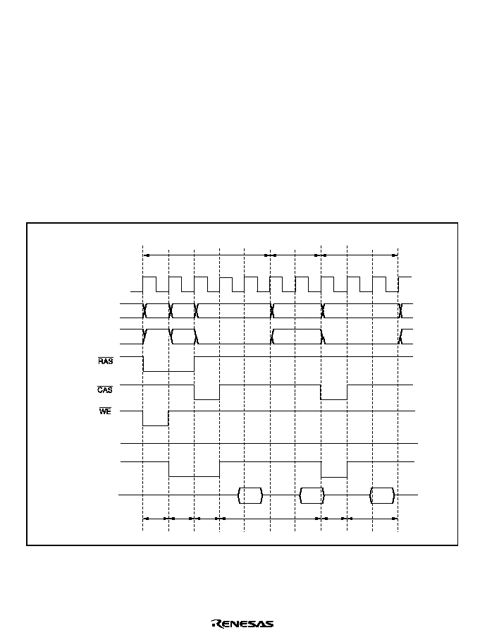
Rev. 2.0, 04/02, page 213 of 906
Note, however, the next continuous synchronous DRAM space access is a full access if:
∑
a refresh operation is initiated in the RAS down state
∑
self-refreshing is performed
∑
the chip enters software standby mode
∑
the external bus is released
∑
the BE bit is cleared to 0
∑
the mode register of the synchronous DRAM is set
There is synchronous DRAM in which time of the active state of each bank is restricted. If it is not
guaranteed that other row address are accessed in a period in which program execution ensures the
value (software standby, sleep, etc.), auto refresh or self refresh must be set, and the restrictions of
the maximum active state time of each bank must be satisfied. When refresh is not used, programs
must be developed so that the bank is not in the active state for more than the specified time.
T
p
Address bus
External address
Column address
Column address 2
External address
Row
address
Column
address
Data bus
T
r
T
c1
T
cl
T
c2
T
c1
T
c2
Continuous synchronous
DRAM space read
Continuous synchronous
DRAM space read
External
space read
T
2
T
cl
T
1
CKE
High
PALL
ACTV READ
NOP
NOP
READ
DQMU, DQML
Precharge-sel
Row
address
¯
Figure 6.53 Example of Operation Timing in RAS Down Mode
(BE = 1, CAS Latency 2)

Rev. 2.0, 04/02, page 214 of 906
6.7.13
Refresh Control
This LSI is provided with a synchronous DRAM refresh control function. Auto refreshing is used.
In addition, self-refreshing can be executed when the chip enters the software standby state.
Refresh control is enabled when any area is designated as continuous synchronous DRAM space
in accordance with the setting of bits RMTS2 to RMTS0 in DRAMCR.
Auto Refreshing: To select auto refreshing, set the RFSHE bit to 1 in REFCR.
With auto refreshing, RTCNT counts up using the input clock selected by bits RTCK2 to RTCK0
in REFCR, and when the count matches the value set in RTCOR (compare match), refresh control
is performed. At the same time, RTCNT is reset and starts counting up again from H'00.
Refreshing is thus repeated at fixed intervals determined by RTCOR and bits RTCK2 to RTCK0.
Set a value in RTCOR and bits RTCK2 to RTCK0 that will meet the refreshing interval
specification for the synchronous DRAM used.
When bits RTCK2 to RTCK0 are set, RTCNT starts counting up. RTCNT and RTCOR settings
should therefore be completed before setting bits RTCK2 to RTCK0. Auto refresh timing is shown
in figure 6.54.
Since the refresh counter operation is the same as the operation in the DRAM interface, see
section 6.6.12, Refresh Control.
When the continuous synchronous DRAM space is set, access to external space other than
continuous synchronous DRAM space cannot be performed in parallel during the auto refresh
period, since the setting of the CBRM bit of REFCR is ignored.
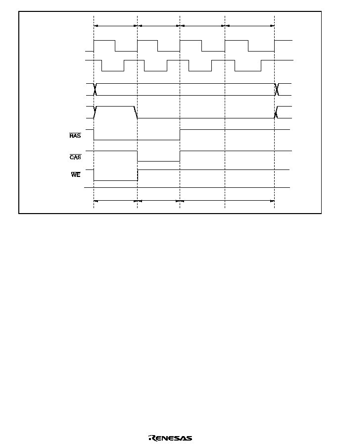
Rev. 2.0, 04/02, page 215 of 906
TRp
SDRAM
CKE
PALL
NOP
REF
Address bus
TRr
TRc1
TRc2
Precharge-sel
High
Figure 6.54 Auto Refresh Timing
When the interval specification from the PLL command to the REF command cannot be satisfied,
setting the RCW1 and RCW0 bits of REFCR enables one to three wait states to be inserted after
the T
Rp
cycle that is set by the TPC1 and TPC0 bits of DRACCR. Set the optimum number of
waits according to the synchronous DRAM connected and the operating frequency of this LSI.
Figure 6.55 shows the timing when one wait state is inserted. Since the setting of bits TPC1 and
TPC0 of DRACCR is also valid in refresh cycles, the command interval can be extended by the
RCW1 and RCW0 bits after the precharge cycles.
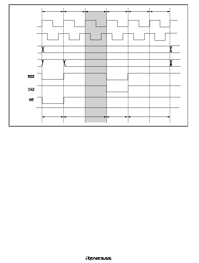
Rev. 2.0, 04/02, page 216 of 906
T
Rp1
¯
SDRAM¯
CKE
PALL
NOP
REF
NOP
Address bus
T
Rp2
T
Rrw
T
Rr
T
Rc1
T
Rc2
Precharge-sel
High
Figure 6.55 Auto Refresh Timing
(TPC = 1, TPC0 = 1, RCW1 = 0, RCW0 = 1)
When the interval specification from the REF command to the ACTV cannot be satisfied, setting
the RLW1 and RLW0 bits of REFCR enables one to three wait states to be inserted in the refresh
cycle. Set the optimum number of waits according to the synchronous DRAM connected and the
operating frequency of this LSI. Figure 6.56 shows the timing when one wait state is inserted.
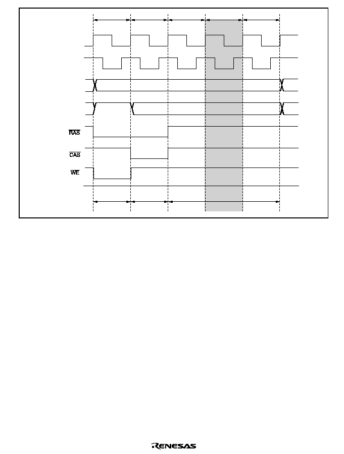
Rev. 2.0, 04/02, page 217 of 906
T
Rp
¯
SDRAM¯
CKE
PALL
REF
NOP
Address bus
T
Rr
T
Rr1
T
Rcw
T
Rc2
Precharge-sel
High
Figure 6.56 Auto Refresh Timing
(TPC = 0, TPC0 = 0, RLW1 = 0, RLW0 = 1)
Self-Refreshing: A self-refresh mode (battery backup mode) is provided for synchronous DRAM
as a kind of standby mode. In this mode, refresh timing and refresh addresses are generated within
the synchronous DRAM.
To select self-refreshing, set the RFSHE bit to 1 in REFCR. When a SLEEP instruction is
executed to enter software standby mode, the SELF command is issued, as shown in figure 6.57.
When software standby mode is exited, the SLFRF bit in REFCR is cleared to 0 and self-refresh
mode is exited automatically. If an auto refresh request occurs when making a transition to
software standby mode, auto refreshing is executed, then self-refresh mode is entered.
When using self-refresh mode, the OPE bit must not be cleared to 0 in SBYCR.
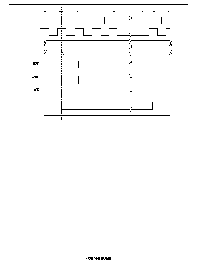
Rev. 2.0, 04/02, page 218 of 906
T
Rp
SDRAM¯
Precharge-sel
Address bus
T
Rr
Software standby
T
Rc2
CKE
NOP
SELF
PALL
Figure 6.57 Self-Refresh Timing
(TPC1 = 1, TPC0 = 0, RCW1 = 0, RCW0 = 0, RLW1 = 0, RLW0 = 0)
In some synchronous DRAMs provided with a self-refresh mode, the interval between clearing
self-refreshing and the next command is specified. A setting can be made in bits TPCS2 to TPCS0
in REFCR to make the precharge time after self-refreshing from 1 to 7 states longer than the
normal precharge time. In this case, too, normal precharging is performed according to the setting
of bits TPC1 and TPC0 in DRACCR, and therefore a setting should be made to give the optimum
post-self-refresh precharge time, including this time. Figure 6.58 shows an example of the timing
when the precharge time after self-refreshing is extended by 2 states.
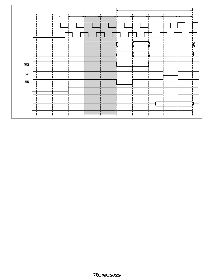
Rev. 2.0, 04/02, page 219 of 906
T
Rc2
¯
SDRAM
¯
CKE
NOP
PALL
NOP
ACTV
NOP
NOP
DQMU, DQML
Data bus
Address bus
T
Rp1
T
Rp2
T
p
T
r
T
c1
T
cl
T
c2
Row address
Column address
Column address
Precharge-sel
Row address
Continuous synchronous DRAM space write
Software
standby
Figure 6.58 Example of Timing when Precharge Time after Self-Refreshing Is Extended
by 2 States (TPCS2 to TPCS0 = H'2, TPC1 = 0, TPC0 = 0, CAS Latency 2)
Refreshing and All-Module-Clocks-Stopped Mode: In this LSI, if the ACSE bit is set to 1 in
MSTPCRH, and then a SLEEP instruction is executed with the setting for all peripheral module
clocks to be stopped (MSTPCR = H'FFFF) or for operation of the 8-bit timer module alone
(MSTPCR = H'FFFE), and a transition is made to the sleep state, the all-module-clocks-stopped
mode is entered, in which the bus controller and I/O port clocks are also stopped.
As the bus controller clock is also stopped in this mode, auto refreshing is not executed. If
synchronous DRAM is connected externally and DRAM data is to be retained in sleep mode, the
ACSE bit must be cleared to 0 in MSTPCR.
Software Standby: When a transition is made to normal software standby, the PLL command is
not output. If synchronous DRAM is connected and DRAM data is to be retained in software
standby, self-refreshing must be set.
6.7.14
Mode Register Setting of Synchronous DRAM
To use synchronous DRAM, mode must be set after power-on. to set mode, set the RMTS2 to
RMTS0 bits in DRAMCR to H'5 and enable the synchronous DRAM mode register setting. After
that, access the continuous synchronous DRAM space in bytes. When the value to be set in the
synchronous DRAM mode register is X, value X is set in the synchronous DRAM mode register
by writing to the continuous synchronous DRAM space of address H'400000 + X for 8-bit bus
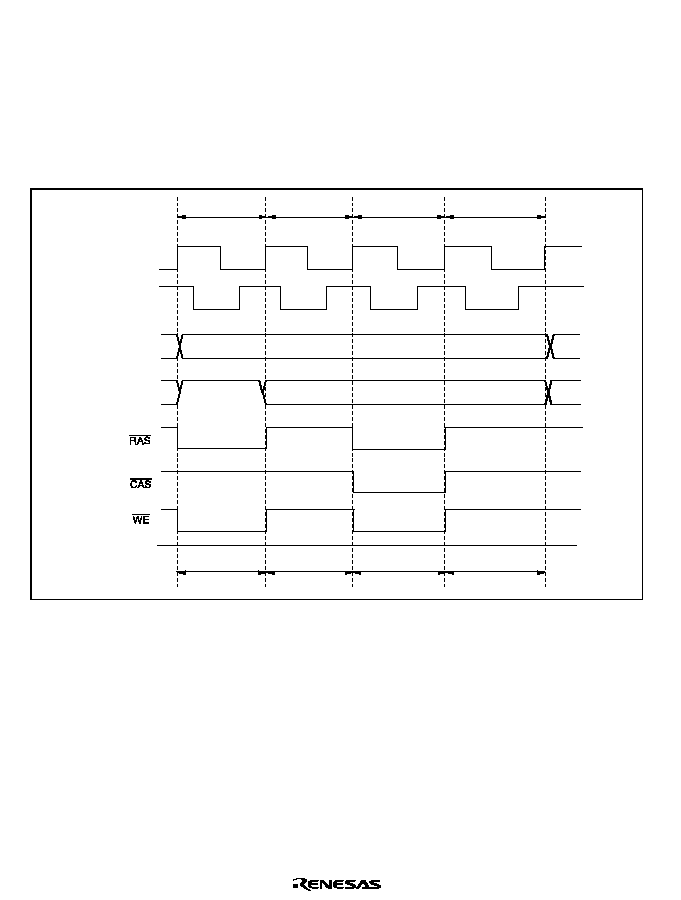
Rev. 2.0, 04/02, page 220 of 906
configuration synchronous DRAM and by writing to the continuous synchronous DRAM space of
address H'400000 + 2X for 16-bit bus configuration synchronous DRAM.
The value of the address signal is fetched at the issuance time of the MRS command as the setting
value of the mode register in the synchronous DRAM. Mode of burst read/burst write in the
synchronous DRAM is not supported by this LSI. For setting the mode register of the
synchronous DRAM, set the burst read/single write with the burst length of 1. Figure 6.59 shows
the setting timing of the mode in the synchronous DRAM.
T
p
¯
SDRAM¯
CKE
PALL
MRS
NOP
NOP
Address bus
T
r
T
c1
T
c2
Mode setting value
Mode setting value
Precharge-sel
High
Figure 6.59 Synchronous DRAM Mode Setting Timing

Rev. 2.0, 04/02, page 221 of 906
6.7.15
DMAC and EXDMAC Single Address Transfer Mode and Synchronous DRAM
Interface
When burst mode is selected on the synchronous DRAM interface, the
'$&. and ('$&. output
timing can be selected with the DDS and EDDS bits in DRAMCR. When continuous synchronous
DRAM space is accessed in DMAC/EXDMAC single address mode at the same time, these bits
select whether or not burst access is to be performed. The establishment time for the read data can
be extended in the clock suspend mode irrespective of the settings of the DDS and EDDS bits.
(1) Output Timing of
'$&
'$&.
. or ('$&.
('$&.
When DDS = 1 or EDDS = 1: Burst access is performed by determining the address only,
irrespective of the bus master. With the synchronous DRAM interface, the
'$&. or ('$&.
output goes low from the T
c1
state.
Figure 6.60 shows the
'$&. or ('$&. output timing for the synchronous DRAM interface
when DDS = 1 or EDDS = 1.

Rev. 2.0, 04/02, page 222 of 906
T
p
¯
SDRAM¯
Read
CKE
PALL
ACTV
READ
NOP
DQMU, DQML
Data bus
Address bus
T
r
T
c1
T
cl
T
c2
Row address
Column address
Column address
Precharge-sel
Row address
High
Write
CKE
PALL
ACTV
NOP
NOP
WRIT
DQMU, DQML
or
Data bus
High
Figure 6.60 Example of
'$&
'$&.
./('$&.
('$&. Output Timing when DDS = 1 or EDDS = 1

Rev. 2.0, 04/02, page 223 of 906
When DDS = 0 or EDDS = 0: When continuous synchronous DRAM space is accessed in
DMAC or EXDMAC single address transfer mode, full access (normal access) is always
performed. With the synchronous DRAM interface, the
'$&. or ('$&. output goes low from
the T
r
state.
In modes other than DMAC or EXDMAC single address transfer mode, burst access can be used
when accessing continuous synchronous DRAM space.
Figure 6.61 shows the
'$&. or ('$&. output timing for the synchronous DRAM interface
when DDS = 0 or EDDS = 0.
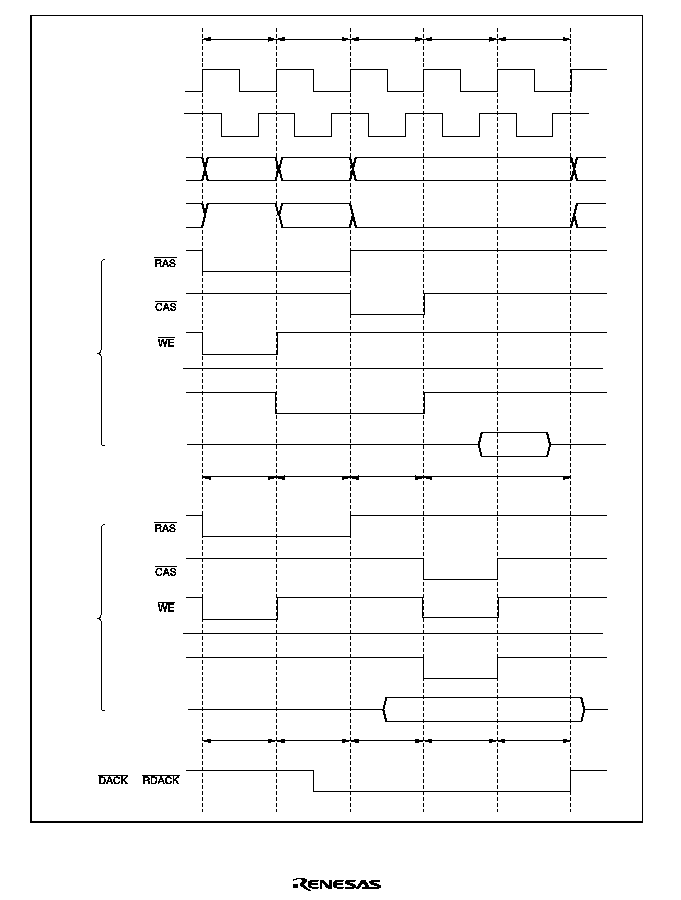
Rev. 2.0, 04/02, page 224 of 906
T
p
¯
SDRAM¯
Read
CKE
PALL
ACTV
READ
NOP
DQMU, DQML
Data bus
Address bus
T
r
T
c1
T
cl
T
c2
Row address
Column address
Column address
Precharge-sel
Row address
High
Write
CKE
PALL
ACTV
NOP
NOP
WRIT
DQMU, DQML
or
Data bus
High
Figure 6.61 Example of
'$&
'$&.
./('$&.
('$&. Output Timing when DDS = 0 or EDDS = 0
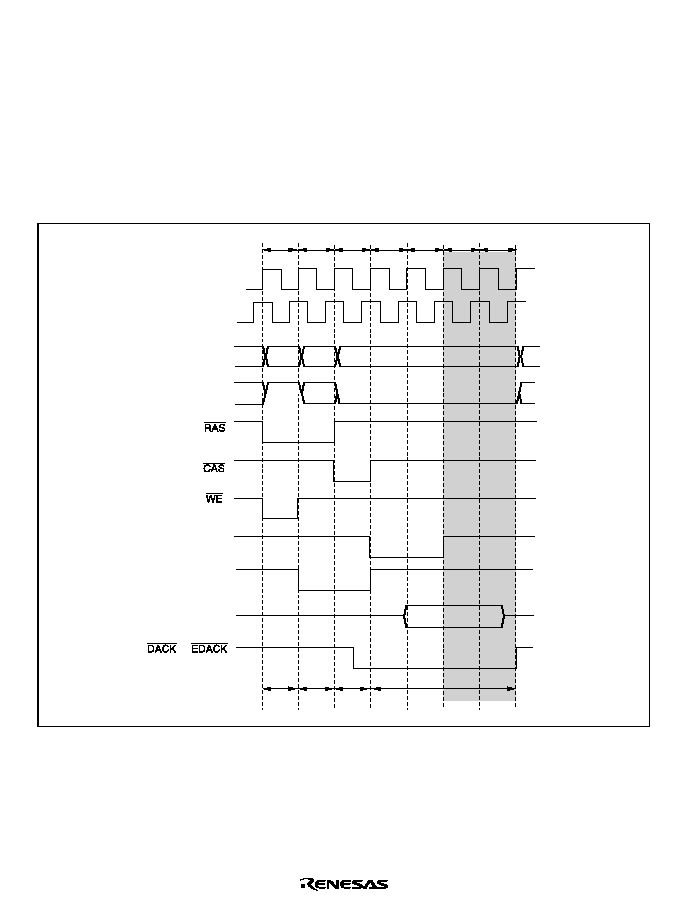
Rev. 2.0, 04/02, page 225 of 906
(2) Read Data Extension
If the CKSPE bit is set to 1 in DRACCR when the continuous synchronous DRAM space is read-
accessed in DMAC/EXDMAC single address mode, the establishment time for the read data can
be extended by clock suspend mode. The number of states for insertion of the read data extension
cycle (Tsp) is set in bits RDXC1 and RDXC0 in DRACCR. Be sure to set the OEE bit to 1 in
DRAMCR when the read data will be extended. The extension of the read data is not in
accordance with the bits DDS and EDDS.
Figure 6.62 shows the timing chart when the read data is extended by two cycles.
Address bus
¯
SDRAM¯
Column address
Row
address
Row
address
Column
address
Data bus
T
p
T
r
T
c2
T
cl
T
sp2
T
sp1
T
c1
CKE
PALL ACTV
NOP
READ
DQMU, DQML
or
Precharge-sel
Figure 6.62 Example of Timing when the Read Data is Extended by Two States
(DDS = 1, or EDDS = 1, RDXC1 = 0, RDXC0 = 1, CAS Latency 2)

Rev. 2.0, 04/02, page 226 of 906
6.8
Burst ROM Interface
In this LSI, external space areas 0 and 1 can be designated as burst ROM space, and burst ROM
interfacing performed. The burst ROM space interface enables ROM with burst access capability
to be accessed at high speed.
Areas 1 and 0 can be designated as burst ROM space by means of bits BSRM1 and BSRM0 in
BROMCR. Continuous burst accesses of 4, 8, 16, or 32 words can be performed, according to the
setting of the BSWD11 and BSWD10 bits in BROMCR. From 1 to 8 states can be selected for
burst access.
Settings can be made independently for area 0 and area 1.
In burst ROM interface space, burst access covers only CPU read accesses.
6.8.1
Basic Timing
The number of access states in the initial cycle (full access) on the burst ROM interface is
determined by the basic bus interface settings in ASTCR, ABWCR, WTCRA, WTCRB, and
CSACRH. When area 0 or area 1 is designated as burst ROM interface space, the settings in
RDNCR and CSACRL are ignored.
From 1 to 8 states can be selected for the burst cycle, according to the settings of bits BSTS02 to
BSTS00 and BSTS12 to BSTS10 in BROMCR. Wait states cannot be inserted. Burst access of up
to 32 words is performed, according to the settings of bits BSTS01, BSTS00, BSTS11, and
BSTS10 in BROMCR.
The basic access timing for burst ROM space is shown in figures 6.63 and 6.64.
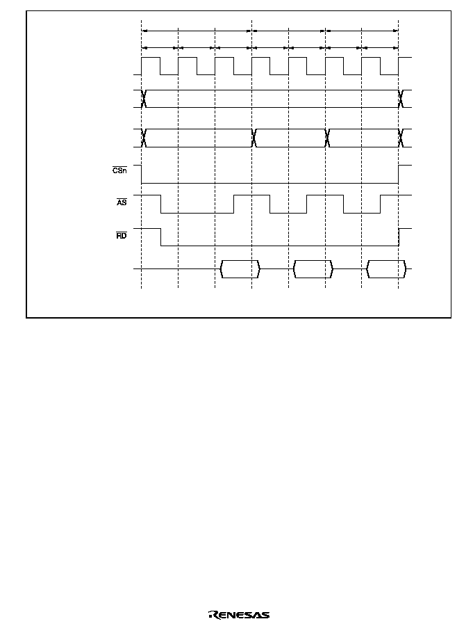
Rev. 2.0, 04/02, page 227 of 906
T
1
Upper address bus
Lower address bus
¯
Data bus
T
2
T
3
T
1
T
2
T
1
Full access
T
2
Burst access
Note: n = 1 and 0
Figure 6.63 Example of Burst ROM Access Timing
(ASTn = 1, 2-State Burst Cycle)

Rev. 2.0, 04/02, page 228 of 906
T
1
Upper address bus
Lower address bus
¯
Data bus
T
2
T
1
T
1
Full access
Burst access
Note: n = 1 and 0
Figure 6.64 Example of Burst ROM Access Timing
(ASTn = 0, 1-State Burst Cycle)
6.8.2
Wait Control
As with the basic bus interface, either program wait insertion or pin wait insertion using the
:$,7
pin can be used in the initial cycle (full access) on the burst ROM interface. See section 6.5.4,
Wait Control. Wait states cannot be inserted in a burst cycle.
6.8.3
Write Access
When a write access to burst ROM interface space is executed, burst access is interrupted at that
point and the write access is executed in line with the basic bus interface settings. Write accesses
are not performed in burst mode even though burst ROM space is designated.
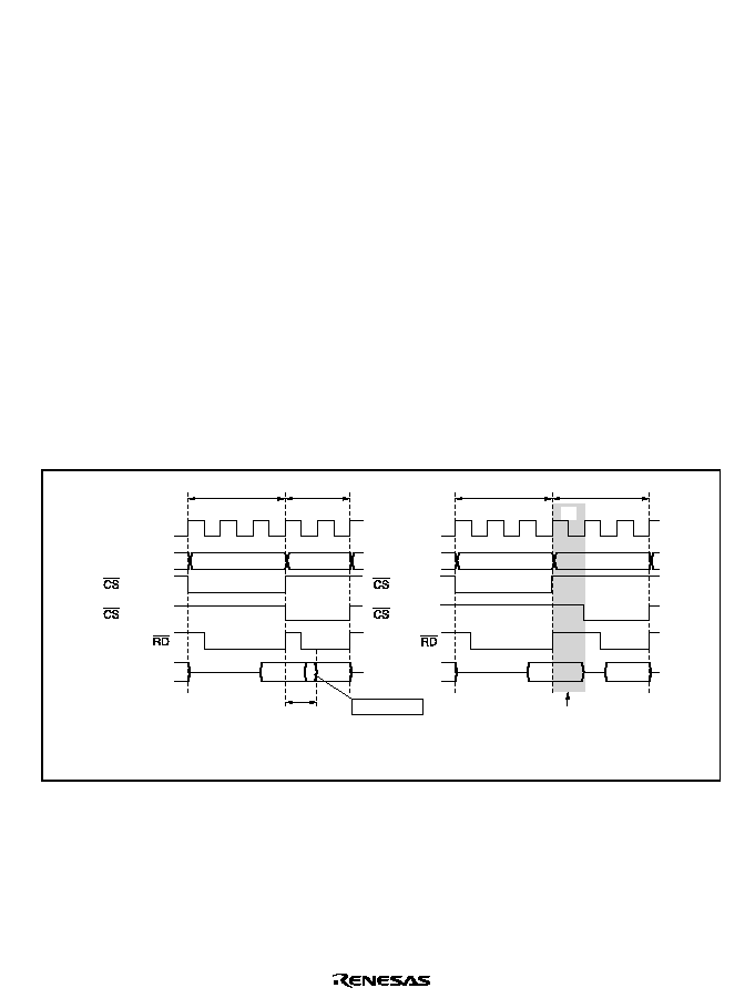
Rev. 2.0, 04/02, page 229 of 906
6.9
Idle Cycle
6.9.1
Operation
When this LSI accesses external space, it can insert an idle cycle (T
i
) between bus cycles in the
following three cases: (1) when read accesses in different areas occur consecutively, (2) when a
write cycle occurs immediately after a read cycle, and (3) when a read cycle occurs immediately
after a write cycle (in the H8S/2678R Series, it cannot insert an idle cycle in the condition (3)).
Insertion of a 1-state or 2-state idle cycle can be selected with the IDLC bit in BCR. By inserting
an idle cycle it is possible, for example, to avoid data collisions between ROM, etc., with a long
output floating time, and high-speed memory, I/O interfaces, and so on.
Consecutive Reads in Different Areas: If consecutive reads in different areas occur while the
ICIS1 bit is set to 1 in BCR, an idle cycle is inserted at the start of the second read cycle.
Figure 6.65 shows an example of the operation in this case. In this example, bus cycle A is a read
cycle for ROM with a long output floating time, and bus cycle B is a read cycle for SRAM, each
being located in a different area. In (a), an idle cycle is not inserted, and a collision occurs in bus
cycle B between the read data from ROM and that from SRAM. In (b), an idle cycle is inserted,
and a data collision is prevented.
T
1
Address bus
¯
Bus cycle A
,
y
Data bus
T
2
T
3
T
1
T
2
Bus cycle B
Long output floating time
Data collision
(a) No idle cycle insertion
(ICIS1 = 0)
T
1
Address bus
¯
Bus cycle A
Data bus
T
2
T
3
T
i
T
1
Bus cycle B
(b) Idle cycle insertion
(ICIS1 = 1, initial value)
T
2
(area A)
(area B)
(area A)
(area B)
Idle cycle
Figure 6.65 Example of Idle Cycle Operation
(Consecutive Reads in Different Areas)
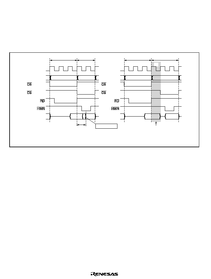
Rev. 2.0, 04/02, page 230 of 906
Write after Read: If an external write occurs after an external read while the ICIS0 bit is set to 1
in BCR, an idle cycle is inserted at the start of the write cycle.
Figure 6.66 shows an example of the operation in this case. In this example, bus cycle A is a read
cycle for ROM with a long output floating time, and bus cycle B is a CPU write cycle. In (a), an
idle cycle is not inserted, and a collision occurs in bus cycle B between the read data from ROM
and the CPU write data. In (b), an idle cycle is inserted, and a data collision is prevented.
T
1
Address bus
¯
Bus cycle A
Data bus
T
2
T
3
T
1
T
2
Bus cycle B
Long output floating time
Data collision
(a) No idle cycle insertion
(ICIS0 = 0)
T
1
Address bus
¯
Bus cycle A
Data bus
T
2
T
3
T
1
Bus cycle B
(b) Idle cycle insertion
(ICIS0 = 1, initial value)
T
2
(area A)
(area B)
(area A)
(area B)
,
y
Idle cycle
T
i
Figure 6.66 Example of Idle Cycle Operation (Write after Read)
Read after Write: If an external read occurs after an external write while the ICIS2 bit is set to 1
in BCR, an idle cycle is inserted at the start of the read cycle.
Figure 6.67 shows an example of the operation in this case. In this example, bus cycle A is a CPU
write cycle and bus cycle B is a read cycle from an external device. In (a), an idle cycle is not
inserted, and a collision occurs in bus cycle B between the CPU write data and read data from an
external device. In (b), an idle cycle is inserted, and a data collision is prevented.
Note:
In the H8S/2678 Series, an idle cycle cannot be inserted in the condition (3).

Rev. 2.0, 04/02, page 231 of 906
T
1
Address bus
¯
Bus cycle A
Data bus
T
2
T
3
T
1
T
2
Bus cycle B
Long output floating time
Data collision
(a) No idle cycle insertion
(ICIS2 = 0)
T
1
Address bus
¯
Bus cycle A
Data bus
T
2
T
3
T
1
Bus cycle B
(b) Idle cycle insertion
(ICIS2 = 1, initial value)
T
2
,
(area A)
(area B)
(area A)
(area B)
,
y
Idle cycle
T
i
Figure 6.67 Example of Idle Cycle Operation (Read after Write)
Relationship between Chip Select (
&6
&6) Signal and Read (5'
5') Signal: Depending on the
system's load conditions, the
5' signal may lag behind the &6 signal. An example is shown in
figure 6.68. In this case, with the setting for no idle cycle insertion (a), there may be a period of
overlap between the bus cycle A
5' signal and the bus cycle B &6 signal. Setting idle cycle
insertion, as in (b), however, will prevent any overlap between the
5' and &6 signals. In the
initial state after reset release, idle cycle insertion (b) is set.
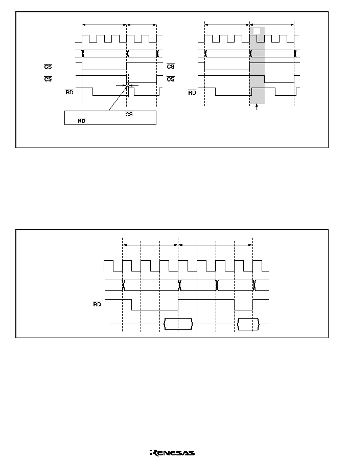
Rev. 2.0, 04/02, page 232 of 906
T
1
Address bus
¯
Bus cycle A
T
2
T
3
T
1
T
2
Bus cycle B
Overlap period between
(area B)
and
may occur
(a) No idle cycle insertion
(ICIS1 = 0)
T
1
Address bus
Idle cycle
¯
Bus cycle A
T
2
T
3
T
i
T
1
Bus cycle B
(b) Idle cycle insertion
(ICIS1 = 1, initial value)
T
2
(area A)
(area B)
(area A)
(area B)
Figure 6.68 Relationship between Chip Select (
$
$) and Read (#
#)
Idle Cycle in Case of DRAM Space Access after Normal Space Access: In a DRAM space
access following a normal space access, the settings of bits ICIS2 (not available in the H8S/2678
Series), ICIS1, ICIS0, and IDLC in BCR are valid. However, in the case of consecutive reads in
different areas, for example, if the second read is a full access to DRAM space, only a T
p
cycle is
inserted, and a T
i
cycle is not. The timing in this case is shown in figure 6.69.
T
1
Address bus
¯
External read
Data bus
T
2
T
3
T
p
T
r
DRAM space read
T
c1
T
c2
Figure 6.69 Example of DRAM Full Access after External Read
(CAST = 0)
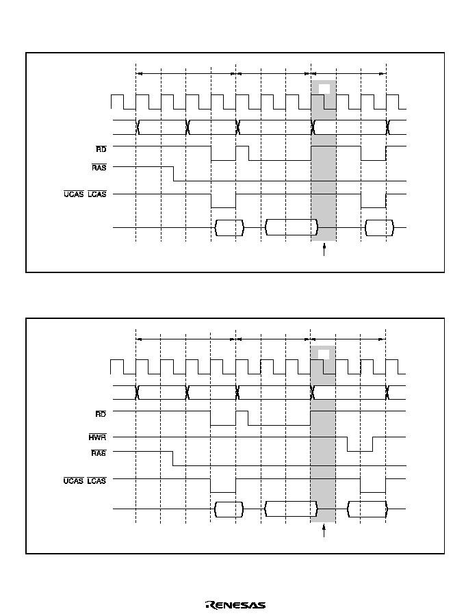
Rev. 2.0, 04/02, page 233 of 906
In burst access in RAS down mode, the settings of bits ICIS2*, ICIS1, ICIS0, and IDLC are valid
and an idle cycle is inserted. The timing in this case is illustrated in figures 6.70 and 6.71.
T
p
Address bus
¯
,
External read
Idle cycle
Data bus
T
r
T
c1
T
c2
T
1
DRAM space read
DRAM space read
T
2
T
c2
T
3
T
i
T
c1
Figure 6.70 Example of Idle Cycle Operation in RAS Down Mode
(Consecutive Reads in Different Areas) (IDLC = 0, RAST = 0, CAST = 0)
T
p
Address bus
¯
,
External read
Idle cycle
Data bus
T
r
T
c1
T
c2
T
1
DRAM space write
DRAM space read
T
2
T
c2
T
3
T
i
T
c1
Figure 6.71 Example of Idle Cycle Operation in RAS Down Mode
(Write after Read) (IDLC = 0, RAST = 0, CAST = 0)
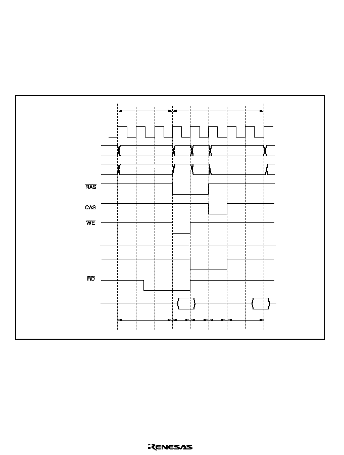
Rev. 2.0, 04/02, page 234 of 906
Idle Cycle in Case of Continuous Synchronous DRAM Space Access after Normal Space
Access: In a continuous synchronous DRAM space access following a normal space access, the
settings of bits ICIS2, ICIS1, ICIS0, and IDLC in BCR are valid. However, in the case of
consecutive reads in different areas, for example, if the second read is a full access to continuous
synchronous DRAM space, only Tp cycle is inserted, and Ti cycle is not. The timing in this case
is shown in figure 6.72.
Note:
In the H8S/2678 Series, the synchronous DRAM interface is not supported.
T
1
Address bus
¯
Column address
Row
address
Row
address
Column
address
Data bus
T
2
T
3
T
p
T
r
T
c2
External space read
Synchronous DRAM space read
T
cl
T
c1
CKE
PALL ACTV
NOP
NOP
READ
DQMU, DQML
Precharge-sel
Figure 6.72 Example of Synchronous DRAM Full Access after External Read
(CAS Latency 2)
In burst access in RAS down mode, the settings of bits ICIS2, ICIS1, ICIS0, and IDLC are valid
and an idle cycle is inserted. However, in read access, note that the timings of DQMU and DQML
differ according to the settings of the IDLC bit. The timing in this case is illustrated in figures
6.73 and 6.74. In write access, DQMU and DQML are not in accordance with the settings of the
IDLC bit. The timing in this case is illustrated in figure 6.75.
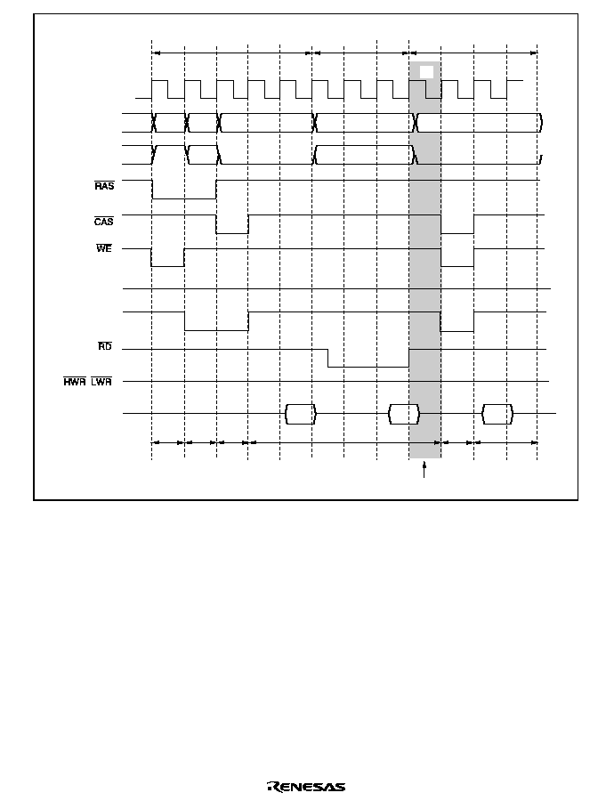
Rev. 2.0, 04/02, page 235 of 906
T
p
Address bus
External address
Column address 1
Column address 2
External address
Row
address
Column
address
Idle cycle
Data bus
T
r
T
c1
T
cl
T
c2
T
3
T
c1
Continuous synchronous
DRAM space read
External space read
Continuous synchronous
DRAM space read
T
2
T
i
T
1
,
CKE
High
High
PALL
ACTV READ
NOP
NOP
READ
DQMU, DQML
T
Cl
T
c2
Precharge-sel
¯
Row
address
Figure 6.73 Example of Idle Cycle Operation in RAS Down Mode
(Read in Different Area) (IDLC = 0, CAS Latency 2)
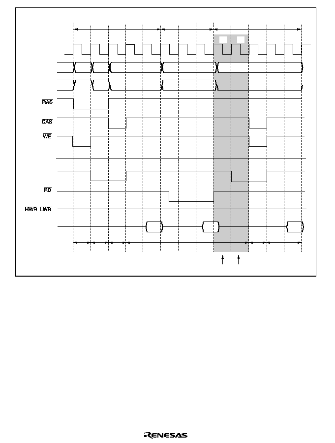
Rev. 2.0, 04/02, page 236 of 906
T
p
Address bus
Idle cycle
Data bus
T
r
T
c1
T
cl
T
c2
T
3
T
c1
Continuous synchronous
DRAM space read
External space read
Continuous synchronous
DRAM space read
T
2
T
i
T
i
T
1
,
CKE
High
High
PALL
ACTV READ
NOP
NOP
READ
DQMU, DQML
T
Cl
T
c2
Precharge-sel
¯
Row
address
Row
address
Column
address
External address
External address
Column address 1
Column address 2
Figure 6.74 Example of Idle Cycle Operation in RAS Down Mode
(Read in Different Area) (IDLC = 1, CAS Latency 2)

Rev. 2.0, 04/02, page 237 of 906
T
p
Address bus
Idle cycle
Data bus
T
r
T
c1
T
cl
T
c2
T
3
T
c1
Continuous synchronous
DRAM space read
External space read
Continuous synchronous
DRAM space write
T
2
T
i
T
1
,
CKE
High
High
PALL
ACTV READ
NOP
NOP
WRIT
DQMU, DQML
T
Cl
T
c2
Precharge-sel
¯
Row
address
Row
address
Column
address
External address
External address
Column address 1
Column address 2
Figure 6.75 Example of Idle Cycle Operation in RAS Down Mode
(Write after Read) (IDLC = 0, CAS Latency 2)
Idle Cycle in Case of Normal Space Access after DRAM Space Access:
∑
Normal space access after DRAM space read access
While the DRMI bit is cleared to 0 in DRACCR, idle cycle insertion after DRAM space access is
disabled. Idle cycle insertion after DRAM space access can be enabled by setting the DRMI bit to
1. The conditions and number of states of the idle cycle to be inserted are in accordance with the
settings of bits ICIS1, ICIS0, and IDLC in BCR are valid. Figures 6.76 and 6.77 show examples of
idle cycle operation when the DRMI bit is set to 1.
When the DRMI bit is cleared to 0, an idle cycle is not inserted after DRAM space access even if
bits ICIS1 and ICIS0 are set to 1.
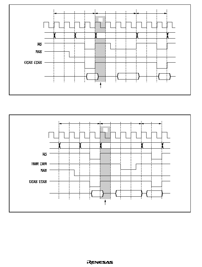
Rev. 2.0, 04/02, page 238 of 906
T
p
Address bus
¯
,
External read
Idle cycle
Data bus
T
r
T
c1
T
c2
T
1
DRAM space read
DRAM space read
T
2
T
c2
T
3
T
i
T
i
T
c1
Figure 6.76 Example of Idle Cycle Operation after DRAM Access
(Consecutive Reads in Different Areas) (IDLC = 0, RAST = 0, CAST = 0)
T
p
Address bus
¯
,
,
External write
Idle cycle
Data bus
T
r
T
c1
T
c2
T
1
DRAM space read
DRAM space read
T
2
T
c2
T
3
T
i
T
c1
Figure 6.77 Example of Idle Cycle Operation after DRAM Access
(Write after Read) (IDLC = 0, RAST = 0, CAST = 0)

Rev. 2.0, 04/02, page 239 of 906
∑
Normal space access after DRAM space write access
While the ICIS2 bit is set to 1 in BCR (there is no ICRS2 bit in the H8S/2678 Series, therefore this
setting cannot be made) and a normal space read access occurs after DRAM space write access,
idle cycle is inserted in the first read cycle. The number of states of the idle cycle to be inserted is
in accordance with the setting of the IDLC bit. It does not depend on the DRMI bit in DRACCR.
Figure 6.78 shows an example of idle cycle operation when the ICIS2 bit is set to 1.
T
p
Address bus
¯
,
,
External space read
Idle cycle
Data bus
T
r
T
c1
T
c2
T
1
DRAM space read
DRAM space read
T
2
T
c2
T
3
T
i
T
c1
Figure 6.78 Example of Idle Cycle Operation after DRAM Write Access
(IDLC = 0, ICIS1 = 0, RAST = 0, CAST = 0)
Idle Cycle in Case of Normal Space Access After Continuous Synchronous DRAM Space
Access:
Note: In the H8S/2678 Series, the synchronous DRAM interface is not supported.
∑
Normal space access after a continuous synchronous DRAM space read access
While the DRMI bit is cleared to 0 in DRACCR, idle cycle insertion after continuous synchronous
DRAM space read access is disabled. Idle cycle insertion after continuous synchronous DRAM
space read access can be enabled by setting the DRMI bit to 1. The conditions and number of
states of the idle cycle to be inserted are in accordance with the settings of bits ICIS1, ICIS0, and
IDLC in RCR. Figure 6.79 shows an example of idle cycle operation when the DRMI bit is set to
1. When the DRMI bit is cleared to 0, an idle cycle is not inserted after continuous synchronous
DRAM space read access even if bits ICIS1 and ICIS0 are set to 1.
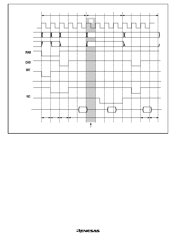
Rev. 2.0, 04/02, page 240 of 906
T
p
Address bus
Idle cycle
Data bus
T
r
T
c1
T
cl
T
c2
T
3
T
i
T
c1
Continuous synchronous
DRAM space read
External space read
Continuous synchronous
DRAM space read
T
2
T
i
T
1
CKE
High
PALL
ACTV READ
NOP
NOP
READ
DQMU, DQML
T
Cl
T
c2
Precharge-sel
¯
External address
External address
Column address 1
Column address 2
Row
address
Row
address
Column
address
Figure 6.79 Example of Idle Cycle Operation after Continuous Synchronous DRAM Space
Read Access (Read between Different Area) (IDLC = 0, CAS Latency 2)
∑
Normal space access after a continuous synchronous DRAM space write access
If a normal space read cycle occurs after a continuous synchronous DRAM space write access
while the ICIS2 bit is set to 1 in BCR, idle cycle is inserted at the start of the read cycle. The
number of states of the idle cycle to be inserted is in accordance with the setting of bit IDLC. It is
not in accordance with the DRMI bit in DRACCR.
Figure 6.80 shows an example of idle cycle operation when the ICIS2 bit is set to 1.
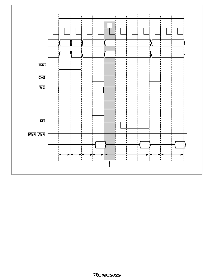
Rev. 2.0, 04/02, page 241 of 906
T
p
Address bus
Idle cycle
Data bus
T
r
T
c1
T
c2
T
3
T
c1
Continuous synchronous
DRAM space write
External space read
Continuous synchronous
DRAM space read
T
2
T
i
T
1
,
CKE
High
PALL
ACTV
NOP WRIT
NOP
NOP
READ
DQMU, DQML
T
Cl
T
c2
Precharge-sel
¯
External address
External address
Column
address
Column address 2
Row
address
Row
address
Column
address
Figure 6.80 Example of Idle Cycle Operation after Continuous Synchronous DRAM Space
Write Access (IDLC = 0, ICIS1 = 0, SDWCD = 1, CAS Latency 2)
Table 6.11 shows whether there is an idle cycle insertion or not in the case of mixed accesses to
normal space and DRAM space/continuous synchronous DRAM space.

Rev. 2.0, 04/02, page 242 of 906
Table 6.11
Idle Cycles in Mixed Accesses to Normal Space and DRAM Continuous
Synchronous DRAM Space
Previous Access
Next Access
ICIS2
*
ICIS1
ICIS0
DRMI
IDLC
Idle cycle
--
0
--
--
--
Disabled
--
1
--
--
0
1 state inserted
Normal space read
(different area)
1
2 states inserted
--
0
--
--
--
Disabled
--
1
--
--
0
1 state inserted
DRAM/continuous
synchronous DRAM
*
space read
1
2 states inserted
--
--
0
--
--
Disabled
--
--
1
--
0
1 state inserted
Normal space write
1
2 states inserted
--
--
0
--
--
Disabled
--
--
1
--
0
1 state inserted
Normal space read
DRAM/continuous
synchronous DRAM
*
space write
1
2 states inserted
--
0
--
--
--
Disabled
--
1
--
0
--
Disabled
1
0
1 state inserted
Normal space read
1
2 states inserted
--
0
--
--
--
Disabled
--
1
--
0
--
Disabled
1
0
1 state inserted
DRAM/continuous
synchronous DRAM
*
space read
1
2 states inserted
--
--
0
--
--
Disabled
--
--
1
0
--
Disabled
1
0
1 state inserted
Normal space write
1
2 states inserted
--
--
0
--
--
Disabled
--
--
1
0
--
Disabled
1
0
1 state inserted
DRAM/continuous
synchronous DRAM
space read
DRAM/continuous
synchronous DRAM
*
space write
1
2 states inserted
0
--
--
--
--
Disabled
1
--
--
--
0
1 state inserted
Normal space read
1
2 states inserted
0
--
--
--
--
Disabled
1
--
--
--
0
1 state inserted
Normal space write
DRAM/continuous
synchronous DRAM
*
space read
1
2 states inserted
Rev. 2.0, 04/02, page 243 of 906
Previous Access
Next Access
ICIS2
*
ICIS1
ICIS0
DRMI
IDLC
Idle cycle
0
--
--
--
--
Disabled
1
--
--
--
0
1 state inserted
Normal space read
1
2 states inserted
0
--
--
--
--
Disabled
1
--
--
--
0
1 state inserted
DRAM/continuous
synchronous DRAM
space write
DRAM/continuous
synchronous DRAM
space read
1
2 states inserted
Note:
In the H8S/2678 Series, the synchronous DRAM interface is not supported.
Setting the DRMI bit in DRACCR to 1 enables an idle cycle to be inserted in the case of
consecutive read and write operations in DRAM/continuous synchronous DRAM space burst
access. Figures 6.81 and 6.82 show an example of the timing for idle cycle insertion in the case of
consecutive read and write accesses to DRAM/continuous synchronous DRAM space.
T
p
Address bus
Idle cycle
Data bus
T
r
T
c1
T
c2
DRAM space write
DRAM space read
T
c2
T
i
T
c1
(
)
,
(
)
(
)
Note: n = 2 to 5
Figure 6.81 Example of Timing for Idle Cycle Insertion in Case of Consecutive Read and
Write Accesses to DRAM Space in RAS Down Mode
Rev. 2.0, 04/02, page 244 of 906
T
p
Address bus
Idle cycle
Data bus
T
r
T
c1
T
cl
T
c2
Continuous synchronous
DRAM space write
Continuous synchronous
DRAM space read
T
c2
T
i
T
c1
CKE
High
PALL
ACTV READ
NOP
WRIT
DQMU, DQML
Precharge-sel
¯
External address
Column
address
Row
address
Column
address
Figure 6.82 Example of Timing for Idle Cycle Insertion in Case of Consecutive Read and
Write Accesses to Continuous Synchronous DRAM Space in RAS Down Mode
(SDWCD = 1, CAS Latency 2)

Rev. 2.0, 04/02, page 245 of 906
6.9.2
Pin States in Idle Cycle
Table 6.12 shows the pin states in an idle cycle.
Table 6.12
Pin States in Idle Cycle
Pins
Pin State
A23 to A0
Contents of following bus cycle
D15 to D0
High impedance
&6Q
(n = 7 to 0)
High
*
1,
*
2
8&$6
,
/&$6
High
*
2
$6
High
5'
High
(
2(
)
High
+:5
,
/:5
High
'$&.Q
(n = 1, 0)
High
('$&.Q
(n = 3 to 0)
High
Notes: 1. Remains low in DRAM space RAS down mode.
2. Remains low in a DRAM space refresh cycle.
6.10
Write Data Buffer Function
This LSI has a write data buffer function for the external data bus. Using the write data buffer
function enables external writes and DMA single address mode transfers to be executed in parallel
with internal accesses. The write data buffer function is made available by setting the WDBE bit
to 1 in BCR.
Figure 6.83 shows an example of the timing when the write data buffer function is used. When this
function is used, if an external write or DMA single address mode transfer continues for two states
or longer, and there is an internal access next, an external write only is executed in the first state,
but from the next state onward an internal access (on-chip memory or internal I/O register
read/write) is executed in parallel with the external write rather than waiting until it ends.
Rev. 2.0, 04/02, page 246 of 906
T
1
Internal address bus
A23 to A0
External write cycle
,
T
2
T
W
T
W
T
3
On-chip memory read
Internal I/O register read
Internal read signal
D15 to D0
External address
Internal memory
External space
write
Internal I/O register address
Figure 6.83 Example of Timing when Write Data Buffer Function is Used
6.11
Bus Release
This LSI can release the external bus in response to a bus request from an external device. In the
external bus released state, internal bus masters except the EXDMAC continue to operate as long
as there is no external access. If any of the following requests are issued in the external bus
released state, the
%5(42 signal can be driven low to output a bus request externally.
∑
When an internal bus master wants to perform an external access
∑
When a refresh request is generated
∑
When a SLEEP instruction is executed to place the chip in software standby mode or all-
module-clocks-stopped mode
6.11.1
Operation
In externally expanded mode, the bus can be released to an external device by setting the BRLE
bit to 1 in BCR. Driving the
%5(4 pin low issues an external bus request to this LSI. When the
%5(4 pin is sampled, at the prescribed timing the %$&. pin is driven low, and the address bus,
data bus, and bus control signals are placed in the high-impedance state, establishing the external
bus released state.

Rev. 2.0, 04/02, page 247 of 906
In the external bus released state, internal bus masters except the EXDMAC can perform accesses
using the internal bus. When an internal bus master wants to make an external access, it
temporarily defers initiation of the bus cycle, and waits for the bus request from the external bus
master to be canceled. If a refresh request is generated in the external bus released state, or if a
SLEEP instruction is executed to place the chip in software standby mode or all-module-clocks-
stopped mode, refresh control and software standby or all-module-clocks-stopped control is
deferred until the bus request from the external bus master is canceled.
If the BREQOE bit is set to 1 in BCR, the
%5(42 pin can be driven low when any of the
following requests are issued, to request cancellation of the bus request externally.
∑
When an internal bus master wants to perform an external access
∑
When a refresh request is generated
∑
When a SLEEP instruction is executed to place the chip in software standby mode or all-
module-clocks-stopped mode
When the
%5(4 pin is driven high, the %$&. pin is driven high at the prescribed timing and the
external bus released state is terminated.
If an external bus release request and external access occur simultaneously, the order of priority is
as follows:
(High) External bus release > External access by internal bus master (Low)
If a refresh request and external bus release request occur simultaneously, the order of priority is
as follows:
(High) Refresh > External bus release (Low)

Rev. 2.0, 04/02, page 248 of 906
6.11.2
Pin States in External Bus Released State
Table 6.13 shows pin states in the external bus released state.
Table 6.13
Pin States in Bus Released State
Pins
Pin State
A23 to A0
High impedance
D15 to D0
High impedance
&6Q
(n = 7 to 0)
High impedance
8&$6
,
/&$6
High impedance
$6
High impedance
5'
High impedance
(
2(
)
High impedance
+:5
,
/:5
High impedance
'$&.Q
(n = 1, 0)
High
('$&.Q
(n = 3 to 0)
High
Rev. 2.0, 04/02, page 249 of 906
6.11.3
Transition Timing
Figure 6.84 shows the timing for transition to the bus released state.
CPU
cycle
External bus released state
External space
access cycle
T
1
T
2
¯
Address bus
,
High-Z
High-Z
High-Z
High-Z
High-Z
[1]
[2]
[3]
[5]
[4]
[6]
[7]
[8]
[1] Low level of
signal is sampled at rise of ¯.
[2] Bus control signal returns to be high at end of external space access cycle.
At least one state from sampling of
signal.
[3]
signal is driven low, releasing bus to external bus master.
[4]
signal state is also sampled in external bus released state.
[5] High level of
signal is sampled.
[6]
signal is driven high, ending external bus release cycle.
[7] When there is external access or refresh request of internal bus master during external
bus release while BREQOE bit is set to 1,
signal goes low.
[8] Normally
signal goes high 1.5 states after rising edge of
signal.
Data bus
Figure 6.84 Bus Released State Transition Timing
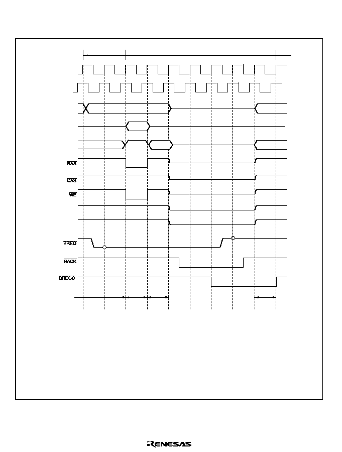
Rev. 2.0, 04/02, page 250 of 906
Figure 6.85 shows the timing for transition to the bus released state with the synchronous DRAM
interface.
CPU
cycle
External bus released state
External space read
T
1
T
2
¯
Address bus
DQMU, DQML
High-Z
High-Z
High-Z
NOP
PALL
NOP
NOP
[1]
[2]
[3]
[5]
[4]
[6]
[8]
[7]
[9]
[1] Low level of BREQ signal is sampled at rise of f.
[2] PLL command is issued.
[3] Bus control signal returns to be high at end of external space access cycle.
At least one state from sampling of BREQ signal.
[4] BACK signal is driven low, releasing bus to external bus master..
[5] BREQ signal state is also sampled in external bus released state.
[6] High level of BREQ signal is sampled.
[7] BACK signal is driven high, ending external bus release cycle.
[8] When there is external access or refresh request of internal bus master during
external bus release while the BREQOE bit is set to 1, BREQO signal goes low.
[9] BREQO signal goes high 1.5 states after rising edge of BACK signal. If BREQO
signal is asserted because of auto-refreshing request, it retains low until auto-refresh cycle starts up.
Data bus
High-Z
Precharge-sel
High-Z
High-Z
CKE
High-Z
High-Z
SDRAM¯
Row
address
Figure 6.85 Bus Release State Transition Timing when Synchronous DRAM Interface

Rev. 2.0, 04/02, page 251 of 906
6.12
Bus Arbitration
This LSI has a bus arbiter that arbitrates bus mastership operations (bus arbitration).
There are four bus masters--the CPU, DTC, DMAC, and EXDMAC--that perform read/write
operations when they have possession of the bus. Each bus master requests the bus by means of a
bus request signal. The bus arbiter determines priorities at the prescribed timing, and permits use
of the bus by means of a bus request acknowledge signal. The selected bus master then takes
possession of the bus and begins its operation.
6.12.1
Operation
The bus arbiter detects the bus masters' bus request signals, and if the bus is requested, sends a bus
request acknowledge signal to the bus master. If there are bus requests from more than one bus
master, the bus request acknowledge signal is sent to the one with the highest priority. When a bus
master receives the bus request acknowledge signal, it takes possession of the bus until that signal
is canceled.
The order of priority of the bus mastership is as follows:
(High) EXDMAC > DMAC > DTC > CPU (Low)
An internal bus access by internal bus masters except the EXDMAC and external bus release, a
refresh when the CBRM bit is 0, and an external bus access by the EXDMAC can be executed in
parallel.
If an external bus release request, a refresh request, and an external access by an internal bus
master occur simultaneously, the order of priority is as follows:
(High) Refresh > EXDMAC > External bus release (Low)
(High) External bus release > External access by internal bus master except EXDMAC (Low)
As a refresh when the CBRM bit in REFCR is cleared to 0 and an external access other than to
DRAM space by an internal bus master can be executed simultaneously, there is no relative order
of priority for these two operations.
6.12.2
Bus Transfer Timing
Even if a bus request is received from a bus master with a higher priority than that of the bus
master that has acquired the bus and is currently operating, the bus is not necessarily transferred
immediately. There are specific timings at which each bus master can relinquish the bus.

Rev. 2.0, 04/02, page 252 of 906
CPU: The CPU is the lowest-priority bus master, and if a bus request is received from the DTC,
DMAC, or EXDMAC, the bus arbiter transfers the bus to the bus master that issued the request.
The timing for transfer of the bus is as follows:
∑
The bus is transferred at a break between bus cycles. However, if a bus cycle is executed in
discrete operations, as in the case of a longword-size access, the bus is not transferred between
the component operations.
∑
With bit manipulation instructions such as BSET and BCLR, the sequence of operations is:
data read (read), relevant bit manipulation operation (modify), write-back (write). The bus is
not transferred during this read-modify-write cycle, which is executed as a series of bus cycles.
∑
If the CPU is in sleep mode, the bus is transferred immediately.
DTC: The DTC sends the bus arbiter a request for the bus when an activation request is generated.
The DTC can release the bus after a vector read, a register information read (3 states), a single data
transfer, or a register information write (3 states). It does not release the bus during a register
information read (3 states), a single data transfer, or a register information write (3 states).
DMAC: The DMAC sends the bus arbiter a request for the bus when an activation request is
generated.
In the case of an external request in short address mode or normal mode, and in cycle steal mode,
the DMAC releases the bus after a single transfer.
In block transfer mode, it releases the bus after transfer of one block, and in burst mode, after
completion of the transfer. However, in the event of an EXDMAC or external bus release request,
which have a higher priority than the DMAC, the bus may be transferred to the bus master even if
block or burst transfer is in progress.
EXDMAC: The EXDMAC sends the bus arbiter a request for the bus when an activation request
is generated.
As the EXDMAC is used exclusively for transfers to and from the external bus, if the bus is
transferred to the EXDMAC, internal accesses by other internal bus masters are still executed in
parallel.
In normal transfer mode or cycle steal transfer mode, the EXDMAC releases the bus after a single
transfer.
In block transfer mode, it releases the bus after transfer of one block, and in burst transfer mode,
after completion of the transfer. By setting the BGUP bit to 1 in EDMDR, it is possible to specify
temporary release of the bus in the event of an external access request from an internal bus master.
For details see section 8, EXDMA Controller.

Rev. 2.0, 04/02, page 253 of 906
External Bus Release: When the
%5(4 pin goes low and an external bus release request is issued
while the BRLE bit is set to 1 in BCR, a bus request is sent to the bus arbiter.
External bus release can be performed on completion of an external bus cycle.
6.13
Bus Controller Operation in Reset
In a reset, this LSI, including the bus controller, enters the reset state immediately, and any
executing bus cycle is aborted.
6.14
Usage Notes
6.14.1
External Bus Release Function and All-Module-Clocks-Stopped Mode
In this LSI, if the ACSE bit is set to 1 in MSTPCR, and then a SLEEP instruction is executed with
the setting for all peripheral module clocks to be stopped (MSTPCR = H'FFFF) or for operation of
the 8-bit timer module alone (MSTPCR = H'FFFE), and a transition is made to the sleep state, the
all-module-clocks-stopped mode is entered in which the clock is also stopped for the bus
controller and I/O ports. In this state, the external bus release function is halted. To use the
external bus release function in sleep mode, the ACSE bit in MSTPCR must be cleared to 0.
Conversely, if a SLEEP instruction to place the chip in all-module-clocks-stopped mode is
executed in the external bus released state, the transition to all-module-clocks-stopped mode is
deferred and performed until after the bus is recovered.
6.14.2
External Bus Release Function and Software Standby
In this LSI, internal bus master operation does not stop even while the bus is released, as long as
the program is running in on-chip ROM, etc., and no external access occurs. If a SLEEP
instruction to place the chip in software standby mode is executed while the external bus is
released, the transition to software standby mode is deferred and performed after the bus is
recovered.
Also, since clock oscillation halts in software standby mode, if
%5(4 goes low in this mode,
indicating an external bus release request, the request cannot be answered until the chip has
recovered from the software standby state.
6.14.3
External Bus Release Function and CBR Refreshing/Auto Refreshing
CBR refreshing/auto refreshing cannot be executed while the external bus is released. Setting the
BREQOE bit to 1 in BCR beforehand enables the
%5(42 signal to be output when a CBR
refresh/auto refresh request is issued.
Note: In the H8S/2678 Series, the auto refresh control is not supported.

Rev. 2.0, 04/02, page 254 of 906
6.14.4
%5(42
%5(42 Output Timing
When the BREQOE bit is set to 1 and the
%5(42 signal is output, %5(42 may go low before
the
%$&. signal.
This will occur if the next external access request or CBR refresh request occurs while internal bus
arbitration is in progress after the chip samples a low level of
%5(4.
6.14.5
Notes on Usage of the Synchronous DRAM
Setting of Synchronous DRAM Interface: The DCTL pin must be fixed to 1 to enable the
synchronous DRAM interface. Do not change the DCTL pin during operation.
Connection Clock: Be sure to set the clock to be connected to the synchronous DRAM to
SDRAM
.
:$,
:$,77 Pin: In the continuous synchronous DRAM space, insertion of the wait state by the :$,7
pin is disabled regardless of the setting of the WAITE bit in BCR.
Bank Control: This LSI cannot carry out the bank control of the synchronous DRAM. All banks
are selected.
Burst Access: The burst read/burst write mode of the synchronous DRAM is not supported.
When setting the mode register of the synchronous DRAM, set to the burst read/single write and
set the burst length to 1.
CAS Latency: When connecting a synchronous DRAM having CAS latency of 1, set the BE bit
to 0 in the DRAMCR.

Rev. 2.0, 04/02, page 255 of 906
Section 7 DMA Controller (DMAC)
This LSI has a built-in DMA controller (DMAC) which can carry out data transfer on up to 4
channels.
7.1
Features
∑
Selectable as short address mode or full address mode
Short address mode
Maximum of 4 channels can be used
Dual address mode or single address mode can be selected
In dual address mode, one of the two addresses, transfer source and transfer destination, is
specified as 24 bits and the other as 16 bits
In single address mode, transfer source or transfer destination address only is specified as 24
bits
In single address mode, transfer can be performed in one bus cycle
Choice of sequential mode, idle mode, or repeat mode for dual address mode and single
address mode
Full address mode
Maximum of 2 channels can be used
Transfer source and transfer destination addresses as specified as 24 bits
Choice of normal mode or block transfer mode
∑
16-Mbyte address space can be specified directly
∑
Byte or word can be set as the transfer unit
∑
Activation sources: internal interrupt, external request, auto-request (depending on transfer
mode)
Six 16-bit timer-pulse unit (TPU) compare match/input capture interrupts
Serial communication interface (SCI_0, SCI_1) transmission complete interrupt, reception
complete interrupt
A/D converter conversion end interrupt
External request
Auto-request
∑
Module stop mode can be set
DMAS260A_010020020400
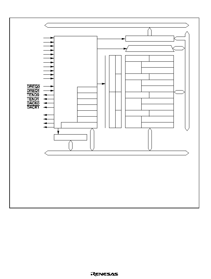
Rev. 2.0, 04/02, page 256 of 906
A block diagram of the DMAC is shown in figure 7.1.
Internal address bus
Address buffer
Processor
Internal interrupts
TGI0A
TGI1A
TGI2A
TGI3A
TGI4A
TGI5A
TXI0
RXI0
TXI1
RXI1
ADI
External pins
Interrupt signals
DMTEND0A
DMTEND0B
DMTEND1A
DMTEND1B
Control logic
DMAWER
DMACR1B
DMACR1A
DMACR0B
DMACR0A
DMATCR
DMABCR
Data buffer
Internal data bus
MAR_0AH
IOAR_0A
ETCR_0A
MAR_0BH
IOAR_0B
ETCR_0B
MAR_1AH
IOAR_1A
ETCR_1A
MAR_1BH
MAR_0AL
MAR_0BL
MAR_1AL
MAR_1BL
IOAR_1B
ETCR_1B
Legend
DMAWER : DMA write enable register
DMATCR : DMA terminal control register
DMABCR : DMA band control register (for all channels)
DMACR
: DMA control register
MAR
: Memory address register
IOAR
: I/O address register
ETCR
: Execute transfer count register
Channel 0
Channel 1
Channel 0A
Channel 0B
Channel 1A
Channel 1B
Module data bus
Figure 7.1 Block Diagram of DMAC

Rev. 2.0, 04/02, page 257 of 906
7.2
Input/Output Pins
Table 7.1 shows the DMAC pin configuration.
Table 7.1
Pin Configuration
Channel
Pin Name
Symbol
I/O
Function
0
DMA request 0
'5(4
Input
Channel 0 external request
DMA transfer acknowledge 0
'$&.
Output
Channel 0 single address
transfer acknowledge
DMA transfer end 0
7(1'
Output
Channel 0 transfer end
1
DMA request 1
'5(4
Input
Channel 1 external request
DMA transfer acknowledge 1
'$&.
Output
Channel 1 single address
transfer acknowledge
DMA transfer end 1
7(1'
Output
Channel 1 transfer end
7.3
Register Descriptions
∑
Memory address register_0AH (MAR_0AH)
∑
Memory address register_0AL (MAR_0AL)
∑
I/O address register_0A (IOAR_0A)
∑
Transfer count register_0A (ECTR_0A)
∑
Memory address register_0BH (MAR_0BH)
∑
Memory address register_0BL (MAR_0BL)
∑
I/O address register_0B (IOAR_0B)
∑
Transfer count register_0B (ECTR_0B)
∑
Memory address register_1AH (MAR_1AH)
∑
Memory address register_1AL (MAR_1AL)
∑
I/O address register_1A (IOAR_1A)
∑
Transfer count register_1A (ETCR_1B)
∑
Memory address register_1BH (MAR_1BH)
∑
Memory address register_1BL (MAR_1BL)
∑
I/O address register_1B (IOAR_1B)
∑
Transfer count register_1B (ETCR_1B)
∑
DMA control register_0A (DMACR_0A)
∑
DMA control register_0B (DMACR_0B)
∑
DMA control register_1A (DMACR_1A)
∑
DMA control register_1B (DMACR_1B)
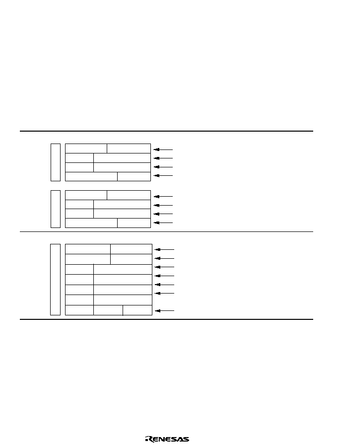
Rev. 2.0, 04/02, page 258 of 906
∑
DMA band control register H (DMABCRH)
∑
DMA band control register L (DMABCRL)
∑
DMA write enable register (DMAWER)
∑
DMA terminal control register (DMATCR)
The functions of MAR, IOAR, ETCR, DMACR, and DMABCR differ according to the transfer
mode (short address mode or full address mode). The transfer mode can be selected by means of
the FAE1 and FAE0 bits in DMABCRH. The register configurations for short address mode and
full address mode of channel 0 are shown in table 7.2.
Table 7.2
Short Address Mode and Full Address Mode (Channel 0)
FAE0
Description
0
Short address mode specified (channels 0A and 0B operate independently)
Channel 0A
MAR_0AH
Specifies transfer source/transfer destination address
Specifies transfer destination/transfer source address
Specifies number of transfers
Specifies transfer size, mode, activation source.
Specifies transfer source/transfer destination address
Specifies transfer destination/transfer source address
Specifies number of transfers
Specifies transfer size, mode, activation source.
IOAR_0A
ETCR_0A
DMACR_0A
Channel 0B
MAR_0BH
MAR_0AL
MAR_0BL
IOAR_0B
ETCR_0B
DMACR_0B
1
Full address mode specified (channels 0A and 0B operate in combination as channel 0)
Channel 0
MAR_0AH
Specifies transfer source address
Specifies transfer destination address
Not used
Not used
Specifies number of transfers
Specifies number of transfers (used in block transfer
mode only)
Specifies transfer size, mode, activation source, etc.
IOAR_0A
ETCR_0A
DMACR_0A
MAR_0BH
MAR_0AL
MAR_0BL
IOAR_0B
ETCR_0B
DMACR_0B
7.3.1
Memory Address Registers (MARA and MARB)
MAR is a 32-bit readable/writable register that specifies the source address (transfer source
address) or destination address (transfer destination address). MAR consists of two 16-bit registers
MARH and MARL. The upper 8 bits of MARH are reserved: they are always read as 0, and
cannot be modified.
The DMA has four MAR registers: MAR_0A in channel 0 (channel 0A), MAR_0B in channel 0
(channel 0B), MAR_1A in channel 1 (channel 1A), and MAR_1B in channel 1 (channel 1B).

Rev. 2.0, 04/02, page 259 of 906
MAR is not initialized by a reset or in standby mode.
Short Address Mode: In short address mode, MARA and MARB operate independently.
Whether MAR functions as the source address register or as the destination address register can be
selected by means of the DTDIR bit in DMACR.
MAR is incremented or decremented each time a byte or word transfer is executed, so that the
address specified by MAR is constantly updated.
Full Address Mode: In full address mode, MARA functions as the source address register, and
MARB as the destination address register.
MAR is incremented or decremented each time a byte or word transfer is executed, so that the
source or destination address is constantly updated.
7.3.2
I/O Address Registers (IOARA and IOARB)
IOAR is a 16-bit readable/writable register that specifies the lower 16 bits of the source address
(transfer source address) or destination address (transfer destination address). The upper 8 bits of
the transfer address are automatically set to H'FF.
The DMA has four IOAR registers: IOAR_0A in channel 0 (channel 0A), IOAR_0B in channel 0
(channel 0B), IOAR_1A in channel 1 (channel 1A), and IOAR_1B in channel 1 (channel 1B).
Whether IOAR functions as the source address register or as the destination address register can
be selected by means of the DTDIR bit in DMACR.
IOAR is not incremented or decremented each time a data transfer is executed, so the address
specified by IOAR is fixed.
IOAR is not initialized by a reset or in standby mode.
IOAR can be used in short address mode but not in full address mode.
7.3.3
Execute Transfer Count Registers (ETCRA and ETCRB)
ETCR is a 16-bit readable/writable register that specifies the number of transfers.
The DMA has four ETCR registers: ETCR_0A in channel 0 (channel 0A), ETCR_0B in channel 0
(channel 0B), ETCR_1A in channel 1 (channel 1A), and ETCR_1B in channel 1 (channel 1B).
ETCR is not initialized by a reset or in standby mode.

Rev. 2.0, 04/02, page 260 of 906
Short Address Mode: The function of ETCR in sequential mode and idle mode differs from that
in repeat mode.
In sequential mode and idle mode, ETCR functions as a 16-bit transfer counter. ETCR is
decremented by 1 each time a transfer is performed, and when the count reaches H'00, the DTE bit
in DMABCRL is cleared, and transfer ends.
In repeat mode, ETCRL functions as an 8-bit transfer counter and ETCRH functions as a transfer
count holding register. ETCRL is decremented by 1 each time a transfer is performed, and when
the count reaches H'00, ETCRL is loaded with the value in ETCRH. At this point, MAR is
automatically restored to the value it had when the count was started. The DTE bit in DMABCRL
is not cleared, and so transfers can be performed repeatedly until the DTE bit is cleared by the
user.
Full Address Mode: The function of ETCR in normal mode differs from that in block transfer
mode.
In normal mode, ETCRA functions as a 16-bit transfer counter. ETCRA is decremented by 1 each
time a data transfer is performed, and transfer ends when the count reaches H'0000. ETCRB is not
used in normal mode.
In block transfer mode, ETCRAL functions as an 8-bit block size counter and ETCRAH functions
as a block size holding register. ETCRAL is decremented by 1 each time a 1-byte or 1-word
transfer is performed, and when the count reaches H'00, ETCRAL is loaded with the value in
ETCRAH. So by setting the block size in ETCRAH and ETCRAL, it is possible to repeatedly
transfer blocks consisting of any desired number of bytes or words.
In block transfer mode, ETCRB functions as a 16-bit block transfer counter. ETCRB is
decremented by 1 each time a block is transferred, and transfer ends when the count reaches
H'0000.

Rev. 2.0, 04/02, page 261 of 906
7.3.4
DMA Control Registers (DMACRA and DMACRB)
DMACR controls the operation of each DMAC channel.
The DMA has four DMACR registers: DMACR_0A in channel 0 (channel 0A), DMACR_0B in
channel 0 (channel 0B), DMACR_1A in channel 1 (channel 1A), and DMACR_1B in channel 1
(channel 1B).
In short address mode, channels A and B operate independently, and in full address mode,
channels A and B operate together. The bit functions in the DMACR registers differ according to
the transfer mode.
Short Address Mode:
∑
DMACR_0A, DMACR_0B, DMACR_1A, and DMARC_1B
Bit
Bit Name
Initial Value
R/W
Description
7
DTSZ
0
R/W
Data Transfer Size
Selects the size of data to be transferred at one
time.
0: Byte-size transfer
1: Word-size transfer
6
DTID
0
R/W
Data Transfer Increment/Decrement
Selects incrementing or decrementing of MAR
after every data transfer in sequential mode or
repeat mode. In idle mode, MAR is neither
incremented nor decremented.
0: MAR is incremented after a data transfer
(Initial value)
∑
When DTSZ = 0, MAR is incremented by 1
∑
When DTSZ = 1, MAR is incremented by 2
1: MAR is decremented after a data transfer
∑
When DTSZ = 0, MAR is decremented by 1
∑
When DTSZ = 1, MAR is decremented by 2

Rev. 2.0, 04/02, page 262 of 906
Bit
Bit Name
Initial Value
R/W
Description
5
RPE
0
R/W
Repeat Enable
Used in combination with the DTIE bit in
DMABCR to select the mode (sequential, idle,
or repeat) in which transfer is to be performed.
∑
When DTIE = 0 (no transfer end interrupt)
0: Transfer in sequential mode
1: Transfer in repeat mode
∑
When DTIE = 1 (with transfer end interrupt)
0: Transfer in sequential mode
1: Transfer in idle mode
4
DTDIR
0
R/W
Data Transfer Direction
Used in combination with the SAE bit in
DMABCR to specify the data transfer direction
(source or destination). The function of this bit is
therefore different in dual address mode and
single address mode.
∑
When SAE = 0
0: Transfer with MAR as source address and
'$&.
pin as write strobe
1: Transfer with
'$&.
pin as read strobe and
MAR as destination address
∑
When SAE = 1
0: Transfer with MAR as source address and
IOAR as destination address
1: Transfer with IOAR as source address and
MAR as destination address
3
2
1
0
DTF3
DTF2
DTF1
DTF0
0
0
0
0
R/W
R/W
R/W
R/W
Data Transfer Factor 3 to 0
These bits select the data transfer factor
(activation source). There are some differences
in activation sources for channel A and channel
B.

Rev. 2.0, 04/02, page 263 of 906
Bit
Bit Name
Initial Value
R/W
Description
∑
Channel A
0000: Setting prohibited
0001: Activated by A/D converter conversion
end interrupt
0010: Setting prohibited
0011: Setting prohibited
0100: Activated by SCI channel 0 transmission
complete interrupt
0101: Activated by SCI channel 0 reception
complete interrupt
0110: Activated by SCI channel 1 transmission
complete interrupt
0111: Activated by SCI channel 1 reception
complete interrupt
1000: Activated by TPU channel 0 compare
match/input capture A interrupt
1001: Activated by TPU channel 1 compare
match/input capture A interrupt
1010: Activated by TPU channel 2 compare
match/input capture A interrupt
1011: Activated by TPU channel 3 compare
match/input capture A interrupt
1100: Activated by TPU channel 4 compare
match/input capture A interrupt
1101: Activated by TPU channel 5 compare
match/input capture A interrupt
1110: Setting prohibited
1111: Setting prohibited

Rev. 2.0, 04/02, page 264 of 906
Bit
Bit Name
Initial Value
R/W
Description
∑
Channel B
0000: Setting prohibited
0001: Activated by A/D converter conversion
end interrupt
0010: Activated by
'5(4
pin rising edge input
(
detected as a low level in the first transfer after
transfer is enabled)
0011: Activated by
'5(4
pin low-level input
0100: Activated by SCI channel 0 transmission
complete interrupt
0101: Activated by SCI channel 0 reception
complete interrupt
0110: Activated by SCI channel 1 transmission
complete interrupt
0111: Activated by SCI channel 1 reception
complete interrupt
1000: Activated by TPU channel 0 compare
match/input capture A interrupt
1001: Activated by TPU channel 1 compare
match/input capture A interrupt
1010: Activated by TPU channel 2 compare
match/input capture A interrupt
1011: Activated by TPU channel 3 compare
match/input capture A interrupt
1100: Activated by TPU channel 4 compare
match/input capture A interrupt
1101: Activated by TPU channel 5 compare
match/input capture A interrupt
1110: Setting prohibited
1111: Setting prohibited
The same factor can be selected for more than
one channel. In this case, activation starts with
the highest-priority channel according to the
relative channel priorities. For relative channel
priorities, see section 7.5.12, Multi-Channel
Operation.

Rev. 2.0, 04/02, page 265 of 906
Full Address Mode:
∑
DMACR_0A and DMACR_1A
Bit
Bit Name
Initial Value
R/W
Description
15
DTSZ
0
R/W
Data Transfer Size
Selects the size of data to be transferred at one
time.
0: Byte-size transfer
1: Word-size transfer
14
13
SAID
SAIDE
0
0
R/W
R/W
Source Address Increment/Decrement
Source Address Increment/Decrement Enable
These bits specify whether source address
register MARA is to be incremented,
decremented, or left unchanged, when data
transfer is performed.
00: MARA is fixed
01: MARA is incremented after a data transfer
∑
When DTSZ = 0, MARA is incremented by 1
∑
When DTSZ = 1, MARA is incremented by 2
10: MARA is fixed
11: MARA is decremented after a data transfer
∑
When DTSZ = 0, MARA is decremented by
1
∑
When DTSZ = 1, MARA is decremented by
2
12
11
BLKDIR
BLKE
0
0
R/W
R/W
Block Direction
Block Enable
These bits specify whether normal mode or
block transfer mode is to be used for data
transfer. If block transfer mode is specified, the
BLKDIR bit specifies whether the source side or
the destination side is to be the block area.
x0: Transfer in normal mode
01: Transfer in block transfer mode (destination
side is block area)
11: Transfer in block transfer mode (source side
is block area)

Rev. 2.0, 04/02, page 266 of 906
Bit
Bit Name
Initial Value
R/W
Description
10
to
8
All 0
R/W
Reserved
These bits can be read from or written to.
However, the write value should always be 0.
Legend
x: Don't care
∑
DMACR_0B and DMACR_1B
Bit
Bit Name
Initial Value
R/W
Description
7
0
R/W
Reserved
This bit can be read from or written to. However,
the write value should always be 0.
6
5
DAID
DAIDE
0
0
R/W
R/W
Destination Address Increment/Decrement
Destination Address Increment/Decrement
Enable
These bits specify whether destination address
register MARB is to be incremented,
decremented, or left unchanged, when data
transfer is performed.
00: MARB is fixed
01: MARB is incremented after a data transfer
∑
When DTSZ = 0, MARB is incremented by 1
∑
When DTSZ = 1, MARB is incremented by 2
10: MARB is fixed
11: MARB is decremented after a data transfer
∑
When DTSZ = 0, MARB is decremented by
1
∑
When DTSZ = 1, MARB is decremented by
2
4
--
0
R/W
Reserved
This bit can be read from or written to. However,
the write value should always be 0.
3
2
1
0
DTF3
DTF2
DTF1
DTF0
0
0
0
0
R/W
R/W
R/W
R/W
Data Transfer Factor 3 to 0
These bits select the data transfer factor
(activation source). The factors that can be
specified differ between normal mode and block
transfer mode.

Rev. 2.0, 04/02, page 267 of 906
Bit
Bit Name
Initial Value
R/W
Description
∑
Normal Mode
0000: Setting prohibited
0001: Setting prohibited
0010: Activated by
'5(4
pin falling edge input
(detected as a low level in the first transfer after
transfer is enabled)
0011: Activated by
'5(4
pin low-level input
010x: Setting prohibited
0110: Auto-request (cycle steal)
0111: Auto-request (burst)
1xxx: Setting prohibited
∑
Block Transfer Mode
0000: Setting prohibited
0001: Activated by A/D converter conversion
end interrupt
0010: Activated by
'5(4
pin falling edge input
(detected as a low level in the first transfer after
transfer is enabled)
0011: Activated by
'5(4
pin low-level input
0100: Activated by SCI channel 0 transmission
complete interrupt
0101: Activated by SCI channel 0 reception
complete interrupt
0110: Activated by SCI channel 1 transmission
complete interrupt
0111: Activated by SCI channel 1 reception
complete interrupt
1000: Activated by TPU channel 0 compare
match/input capture A interrupt
1001: Activated by TPU channel 1 compare
match/input capture A interrupt
1010: Activated by TPU channel 2 compare
match/input capture A interrupt
1011: Activated by TPU channel 3 compare
match/input capture A interrupt
1100:Activated by TPU channel 4 compare
match/input capture A interrupt
1101:Activated by TPU channel 5 compare
match/input capture A interrupt
1110: Setting prohibited
1111: Setting prohibited

Rev. 2.0, 04/02, page 268 of 906
Bit
Bit Name
Initial Value
R/W
Description
The same factor can be selected for more than
one channel. In this case, activation starts with
the highest-priority channel according to the
relative channel priorities. For relative channel
priorities, see section 7.5.12, Multi-Channel
Operation.
Legend
x: Don't care
7.3.5
DMA Band Control Registers H and L (DMABCRH and DMABCRL)
DMABCR controls the operation of each DMAC channel. The bit functions in the DMACR
registers differ according to the transfer mode.
Short Address Mode:
∑
DMABCRH
Bit
Bit Name
Initial Value
R/W
Description
15
FAE1
0
R/W
Full Address Enable 1
Specifies whether channel 1 is to be used in
short address mode or full address mode. In
short address mode, channels 1A and 1B can
be used as independent channels.
0: Short address mode
1: Full address mode
14
FAE0
0
R/W
Full Address Enable 0
Specifies whether channel 0 is to be used in
short address mode or full address mode. In
short address mode, channels 0A and 0B can
be used as independent channels.
0: Short address mode
1: Full address mode
13
SAE1
0
R/W
Single Address Enable 1
Specifies whether channel 1B is to be used for
transfer in dual address mode or single address
mode. This bit is invalid in full address mode.
0: Dual address mode
1: Single address mode

Rev. 2.0, 04/02, page 269 of 906
Bit
Bit Name
Initial Value
R/W
Description
12
SAE0
0
R/W
Single Address Enable 0
Specifies whether channel 0B is to be used for
transfer in dual address mode or single address
mode. This bit is invalid in full address mode.
0: Dual address mode
1: Single address mode
11
10
9
8
DTA1B
DTA1A
DTA0B
DTA0A
0
0
0
0
R/W
R/W
R/W
R/W
Data Transfer Acknowledge 1B
Data Transfer Acknowledge 1A
Data Transfer Acknowledge 0B
Data Transfer Acknowledge 0A
These bits enable or disable clearing when
DMA transfer is performed for the internal
interrupt source selected by the DTF3 to DTF0
bits in DMACR.
It the DTA bit is set to 1 when DTE = 1, the
internal interrupt source is cleared automatically
by DMA transfer. When DTE = 1 and DTA = 1,
the internal interrupt source does not issue an
interrupt request to the CPU or DTC.
If the DTA bit is cleared to 0 when DTE = 1, the
internal interrupt source is not cleared when a
transfer is performed, and can issue an interrupt
request to the CPU or DTC in parallel. In this
case, the interrupt source should be cleared by
the CPU or DTC transfer.
When DTE = 0, the internal interrupt source
issues an interrupt request to the CPU or DTC
regardless of the DTA bit setting.

Rev. 2.0, 04/02, page 270 of 906
∑
DMABCRL
Bit
Bit Name
Initial Value
R/W
Description
7
6
5
4
DTE1B
DTE1A
DTE0B
DTE0A
0
0
0
0
R/W
R/W
R/W
R/W
Data Transfer Enable 1B
Data Transfer Enable 1A
Data Transfer Enable 0B
Data Transfer Enable 0A
If the DTIE bit is set to 1 when DTE = 0, the
DMAC regards this as indicating the end of a
transfer, and issues a transfer end interrupt
request to the CPU or DTC.
When DTE = 1, data transfer is enabled and the
DMAC waits for a request by the activation
source selected by the DTF3 to DTF0 bits in
DMACR. When a request is issued by the
activation source, DMA transfer is executed.
[Clearing conditions]
∑
When initialization is performed
∑
When the specified number of transfers
have been completed in a transfer mode
other than repeat mode
∑
When 0 is written to the DTE bit to forcibly
suspend the transfer, or for a similar reason
[Setting condition]
When 1 is written to the DTE bit after reading
DTE = 0
3
2
1
0
DTIE1B
DTIE1A
DTIE0B
DTIE0A
0
0
0
0
R/W
R/W
R/W
R/W
Data Transfer End Interrupt Enable 1B
Data Transfer End Interrupt Enable 1A
Data Transfer End Interrupt Enable 0B
Data Transfer End Interrupt Enable 0A
These bits enable or disable an interrupt to the
CPU or DTC when transfer ends. If the DTIE bit
is set to 1 when DTE = 0, the DMAC regards
this as indicating the end of a transfer, and
issues a transfer end interrupt request to the
CPU or DTC.
A transfer end interrupt can be canceled either
by clearing the DTIE bit to 0 in the interrupt
handling routine, or by performing processing to
continue transfer by setting the transfer counter
and address register again, and then setting the
DTE bit to 1.

Rev. 2.0, 04/02, page 271 of 906
Full Address Mode:
∑
DMABCRH
Bit
Bit Name
Initial Value
R/W
Description
15
FAE1
0
R/W
Full Address Enable 1
Specifies whether channel 1 is to be used in
short address mode or full address mode.
In full address mode, channels 1A and 1B are
used together as channel 1.
0: Short address mode
1: Full address mode
14
FAE0
0
R/W
Full Address Enable 0
Specifies whether channel 0 is to be used in
short address mode or full address mode.
In full address mode, channels 0A and 0B are
used together as channel 0.
0: Short address mode
1: Full address mode
13
12
--
--
0
0
R/W
R/W
Reserved
These bits can be read from or written to.
However, the write value should always be 0.

Rev. 2.0, 04/02, page 272 of 906
Bit
Bit Name
Initial Value
R/W
Description
11
DTA1
0
R/W
Data Transfer Acknowledge 1
These bits enable or disable clearing when
DMA transfer is performed for the internal
interrupt source selected by the DTF3 to DTF0
bits in DMACR of channel 1.
It the DTA1 bit is set to 1 when DTE1 = 1, the
internal interrupt source is cleared automatically
by DMA transfer. When DTE1 = 1 and DTA1 =
1, the internal interrupt source does not issue
an interrupt request to the CPU or DTC.
It the DTA1 bit is cleared to 0 when DTE1 = 1,
the internal interrupt source is not cleared when
a transfer is performed, and can issue an
interrupt request to the CPU or DTC in parallel.
In this case, the interrupt source should be
cleared by the CPU or DTC transfer.
When DTE1 = 0, the internal interrupt source
issues an interrupt request to the CPU or DTC
regardless of the DTA1 bit setting.
The state of the DTME1 bit does not affect the
above operations.
10
--
0
R/W
Reserved
This bit can be read from or written to. However,
the write value should always be 0.

Rev. 2.0, 04/02, page 273 of 906
Bit
Bit Name
Initial Value
R/W
Description
9
DTA0
0
R/W
Data Transfer Acknowledge 0
These bits enable or disable clearing when
DMA transfer is performed for the internal
interrupt source selected by the DTF3 to DTF0
bits in DMACR of channel 0.
It the DTA0 bit is set to 1 when DTE0 = 1, the
internal interrupt source is cleared automatically
by DMA transfer. When DTE0 = 1 and DTA0 =
1, the internal interrupt source does not issue
an interrupt request to the CPU or DTC.
It the DTA0 bit is cleared to 0 when DTE0 = 1,
the internal interrupt source is not cleared when
a transfer is performed, and can issue an
interrupt request to the CPU or DTC in parallel.
In this case, the interrupt source should be
cleared by the CPU or DTC transfer.
When DTE0 = 0, the internal interrupt source
issues an interrupt request to the CPU or DTC
regardless of the DTA0 bit setting.
The state of the DTME0 bit does not affect the
above operations.
8
--
0
R/W
Reserved
This bit can be read from or written to. However,
the write value should always be 0.

Rev. 2.0, 04/02, page 274 of 906
∑
DMABCRL
Bit
Bit Name
Initial Value
R/W
Description
7
DTME1
0
R/W
Data Transfer Master Enable 1
Together with the DTE1 bit, this bit controls
enabling or disabling of data transfer on
channel 1. When both the DTME1 bit and DTE1
bit are set to 1, transfer is enabled for channel
1.
If channel 1 is in the middle of a burst mode
transfer when an NMI interrupt is generated, the
DTME1 bit is cleared, the transfer is interrupted,
and bus mastership passes to the CPU. When
the DTME1 bit is subsequently set to 1 again,
the interrupted transfer is resumed. In block
transfer mode, however, the DTME1 bit is not
cleared by an NMI interrupt, and transfer is not
interrupted.
[Clearing conditions]
∑
When initialization is performed
∑
When NMI is input in burst mode
∑
When 0 is written to the DTME1 bit
[Setting condition]
When 1 is written to DTME1 after reading
DTME1 = 0

Rev. 2.0, 04/02, page 275 of 906
Bit
Bit Name
Initial Value
R/W
Description
6
DTE1
0
R/W
Data Transfer Enable 1
Enables or disables DMA transfer for the
activation source selected by the DTF3 to DTF0
bits in DMACR of channel 1.
When DTE1 = 0, data transfer is disabled and
the activation source is ignored. If the activation
source is an internal interrupt, an interrupt
request is issued to the CPU or DTC. If the
DTIE1 bit is set to 1 when DTE1 = 0, the DMAC
regards this as indicating the end of a transfer,
and issues a transfer end interrupt request to
the CPU.
When DTE1 = 1 and DTME1 = 1, data transfer
is enabled and the DMAC waits for a request by
the activation source. When a request is issued
by the activation source, DMA transfer is
executed.
[Clearing conditions]
∑
When initialization is performed
∑
When the specified number of transfers
have been completed
∑
When 0 is written to the DTE1 bit to forcibly
suspend the transfer, or for a similar reason
[Setting condition]
When 1 is written to the DTE1 bit after reading
DTE1 = 0

Rev. 2.0, 04/02, page 276 of 906
Bit
Bit Name
Initial Value
R/W
Description
5
DTME0
0
R/W
Data Transfer Master Enable 0
Together with the DTE0 bit, this bit controls
enabling or disabling of data transfer on
channel 0. When both the DTME0 bit and DTE0
bit are set to 1, transfer is enabled for channel
0.
If channel 0 is in the middle of a burst mode
transfer when an NMI interrupt is generated, the
DTME0 bit is cleared, the transfer is interrupted,
and bus mastership passes to the CPU. When
the DTME0 bit is subsequently set to 1 again,
the interrupted transfer is resumed. In block
transfer mode, however, the DTME0 bit is not
cleared by an NMI interrupt, and transfer is not
interrupted.
[Clearing conditions]
∑
When initialization is performed
∑
When NMI is input in burst mode
∑
When 0 is written to the DTME0 bit
[Setting condition]
When 1 is written to DTME0 after reading
DTME0 = 0

Rev. 2.0, 04/02, page 277 of 906
Bit
Bit Name
Initial Value
R/W
Description
4
DTE0
0
R/W
Data Transfer Enable 0
Enables or disables DMA transfer for the
activation source selected by the DTF3 to DTF0
bits in DMACR of channel 0.
When DTE0 = 0, data transfer is disabled and
the activation source is ignored. If the activation
source is an internal interrupt, an interrupt
request is issued to the CPU or DTC. If the
DTE0 bit is cleared to 0 when DTIE0 = 1, the
DMAC regards this as indicating the end of a
transfer, and issues a transfer end interrupt
request to the CPU.
When DTE0 = 1 and DTME0 = 1, data transfer
is enabled and the DMAC waits for a request by
the activation source. When a request is issued
by the activation source, DMA transfer is
executed.
[Clearing conditions]
∑
When initialization is performed
∑
When the specified number of transfers
have been completed
∑
When 0 is written to the DTE0 bit to forcibly
suspend the transfer, or for a similar reason
[Setting condition]
When 1 is written to the DTE0 bit after reading
DTE0 = 0
3
DTIE1B
0
R/W
Data Transfer Interrupt Enable 1B
Enables or disables an interrupt to the CPU or
DTC when transfer on channel 1 is interrupted.
If the DTME1 bit is cleared to 0 when DTIE1B =
1, the DMAC regards this as indicating a break
in the transfer, and issues a transfer break
interrupt request to the CPU or DTC.
A transfer break interrupt can be canceled
either by clearing the DTIE1B bit to 0 in the
interrupt handling routine, or by performing
processing to continue transfer by setting the
DTME1 bit to 1.

Rev. 2.0, 04/02, page 278 of 906
Bit
Bit Name
Initial Value
R/W
Description
2
DTIE1A
0
R/W
Data Transfer End Interrupt Enable 1A
Enables or disables an interrupt to the CPU or
DTC when transfer ends. If the DTE1 bit is
cleared to 0 when DTIE1A= 1, the DMAC
regards this as indicating the end of a transfer,
and issues a transfer end interrupt request to
the CPU or DTC.
A transfer end interrupt can be canceled either
by clearing the DTIE1A bit to 0 in the interrupt
handling routine, or by performing processing to
continue transfer by setting the transfer counter
and address register again, and then setting the
DTE1 bit to 1.
1
DTIE0B
0
R/W
Data Transfer Interrupt Enable 0B
Enables or disables an interrupt to the CPU or
DTC when transfer on channel 1 is interrupted.
If the DTME0 bit is cleared to 0 when DTIE0B=
1, the DMAC regards this as indicating a break
in the transfer, and issues a transfer break
interrupt request to the CPU or DTC.
A transfer break interrupt can be canceled
either by clearing the DTIE0B bit to 0 in the
interrupt handling routine, or by performing
processing to continue transfer by setting the
DTME0 bit to 1.
0
DTIE0A
0
R/W
Data Transfer End Interrupt Enable 0A
Enables or disables an interrupt to the CPU or
DTC when transfer ends. If the DTE0 bit is
cleared to 0 when DTIE0A = 1, the DMAC
regards this as indicating the end of a transfer,
and issues a transfer end interrupt request to
the CPU or DTC.
A transfer end interrupt can be canceled either
by clearing the DTIE0A bit to 0 in the interrupt
handling routine, or by performing processing to
continue transfer by setting the transfer counter
and address register again, and then setting the
DTE0 bit to 1.

Rev. 2.0, 04/02, page 279 of 906
7.3.6
DMA Write Enable Register (DMAWER)
The DMAC can activate the DTC with a transfer end interrupt, rewrite the channel on which the
transfer ended using a DTC chain transfer, and then reactivate the DTC. DMAWER applies
restrictions for changing all bits of DMACR, and specific bits for DMATCR and DMABCR for
the specific channel, to prevent inadvertent rewriting of registers other than those for the channel
concerned. The restrictions applied by DMAWER are valid for the DTC.
Bit
Bit Name
Initial Value
R/W
Description
7
to
4
All 0
-
Reserved
These bits are always read as 0 and cannot be
modified.
3
WE1B
0
R/W
Write Enable 1B
Enables or disables writes to all bits in
DMACR1B, bits 11, 7, and 3 in DMABCR, and
bit 5 in DMATCR.
0: Writes are disabled
1: Writes are enabled
2
WE1A
0
R/W
Write Enable 1A
Enables or disables writes to all bits in
DMACR1A, and bits 10, 6, and 2 in DMABCR.
0: Writes are disabled
1: Writes are enabled
1
WE0B
0
R/W
Write Enable 0B
Enables or disables writes to all bits in
DMACR0B, bits 9, 5, and 1 in DMABCR, and bit
4 in DMATCR.
0: Writes are disabled
1: Writes are enabled
0
WE0A
0
R/W
Write Enable 0A
Enables or disables writes to all bits in
DMACR0A, and bits 8, 4, and 0 in DMABCR.
0: Writes are disabled
1: Writes are enabled
Figure 7.2 shows the transfer areas for activating the DTC with a channel 0A transfer end interrupt
request, and reactivating channel 0A. The address register and count register areas are set again
during the first DTC transfer, then the control register area is set again during the second DTC
chain transfer. When re-setting the control register area, perform masking by setting bits in
DMAWER to prevent modification of the contents of other channels.
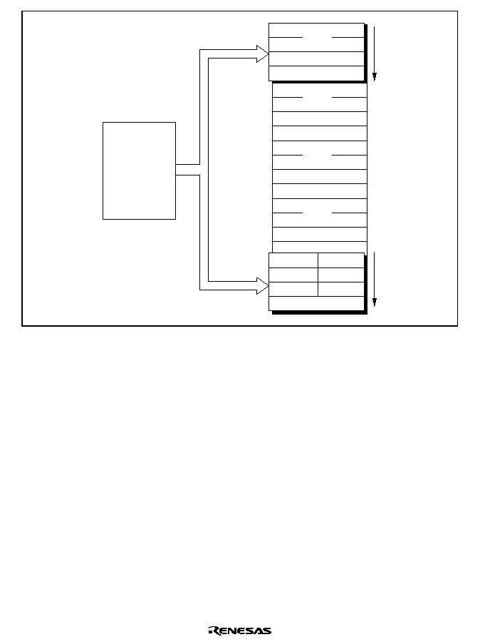
Rev. 2.0, 04/02, page 280 of 906
DTC
MAR_0A
IOAR_0A
ETCR_0A
MAR_0B
IOAR_0B
ETCR_0B
MAR_1A
IOAR_1A
ETCR_1A
MAR_1B
IOAR_1B
ETCR_1B
DMATCR
DMACR_0B
DMACR_1B
DMAWER
DMACR_0A
DMACR_1A
DMABCR
Second transfer area
using chain transfer
First transfer area
Figure 7.2 Areas for Register Re-Setting by DTC (Channel 0A)
Writes by the DTC to bits 15 to 12 (FAE and SAE) in DMABCR are invalid regardless of the
DMAWER settings. These bits should be changed, if necessary, by CPU processing.
In writes by the DTC to bits 7 to 4 (DTE) in DMABCR, 1 can be written without first reading 0.
To reactivate a channel set to full address mode, write 1 to both Write Enable A and Write Enable
B for the channel to be reactivated.
MAR, IOAR, and ETCR can always be written to regardless of the DMAWER settings. When
modifying these registers, the channel to be modified should be halted.

Rev. 2.0, 04/02, page 281 of 906
7.3.7
DMA Terminal Control Register (DMATCR)
DMATCR controls enabling or disabling of output from the DMAC transfer end pin. A port can
be set for output automatically, and a transfer end signal output, by setting the appropriate bit. The
TEND pin is available only for channel B in short address mode. Except for the block transfer
mode, a transfer end signal asserts in the transfer cycle in which the transfer counter contents
reaches 0 regardless of the activation source. In the block transfer mode, a transfer end signal
asserts in the transfer cycle in which the block counter contents reaches 0.
Bit
Bit Name
Initial Value
R/W
Description
7
6
0
0
Reserved
These bits are always read as 0 and cannot be
modified.
5
TEE1
0
R/W
Transfer End Enable 1
Enables or disables transfer end pin 1 (
7(1'
)
output.
0:
7(1'
pin output disabled
1:
7(1'
pin output enabled
4
TEE0
0
R/W
Transfer End Enable 0
Enables or disables transfer end pin 0 (
7(1'
)
output.
0:
7(1'
pin output disabled
1:
7(1'
pin output enabled
3
to
0
All 0
Reserved
These bits are always read as 0 and cannot be
modified.
Rev. 2.0, 04/02, page 282 of 906
7.4
Activation Sources
DMAC activation sources consist of internal interrupt requests, external requests, and auto-
requests. The DMAC activation sources that can be specified depend on the transfer mode and
channel, as shown in table 7.3.
Table 7.3
DMAC Activation Sources
Short Address Mode
Full Address Mode
Activation Source
Channels
0A and 1A
Channels
0B and 1B
Normal
Mode
Block
Transfer
Mode
ADI
X
TXI0
X
RXI0
X
TXI1
X
RXI1
X
TGI0A
X
TGI1A
X
TGI2A
X
TGI3A
X
TGI4A
X
Internal
interrupts
TGI5A
X
'5(4
pin falling edge input
X
External
requests
'5(4
pin low-level input
X
Auto-request
X
X
X
Legend
:
Can be specified
X:
Cannot be specified
7.4.1
Activation by Internal Interrupt Request
An interrupt request selected as a DMAC activation source can also simultaneously generate an
interrupt request for the CPU or DTC. For details, see section 5, Interrupt Controller.
With activation by an internal interrupt request, the DMAC accepts the interrupt request
independently of the interrupt controller. Consequently, interrupt controller priority settings are
irrelevant.

Rev. 2.0, 04/02, page 283 of 906
If the DMAC is activated by a CPU interrupt source or an interrupt request that is not used as a
DTC activation source (DTA = 1), the interrupt request flag is cleared automatically by the DMA
transfer. With ADI, TXI and RXI interrupts, however, the interrupt source flag is not cleared
unless the relevant register is accessed in a DMA transfer. If the same interrupt is used as an
activation source for more than one channel, the interrupt request flag is cleared when the highest-
priority channel is activated. Transfer requests for other channels are held pending in the DMAC,
and activation is carried out in order of priority.
When DTE = 0 after completion of a transfer, an interrupt request from the selected activation
source is not sent to the DMAC, regardless of the DTA bit setting. In this case, the relevant
interrupt request is sent to the CPU or DTC.
When an interrupt request signal for DMAC activation is also used for an interrupt request to the
CPU or DTC activation (DTA = 0), the interrupt request flag is not cleared by the DMAC.
7.4.2
Activation by External Request
If an external request (
'5(4 pin) is specified as a DMAC activation source, the relevant port
should be set to input mode in advance. Level sensing or edge sensing can be used for external
requests.
External request operation in normal mode of short address mode or full address mode is
described below.
When edge sensing is selected, a byte or word is transferred each time a high-to-low transition is
detected on the
'5(4 pin. The next data transfer may not be performed if the next edge is input
before data transfer is completed.
When level sensing is selected, the DMAC stands by for a transfer request while the
'5(4 pin is
held high. While the
'5(4 pin is held low, transfers continue in succession, with the bus being
released each time a byte or word is transferred. If the
'5(4 pin goes high in the middle of a
transfer, the transfer is interrupted and the DMAC stands by for a transfer request.
7.4.3
Activation by Auto-Request
Auto-request is activated by register setting only, and transfer continues to the end. With auto-
request activation, cycle steal mode or burst mode can be selected.
In cycle steal mode, the DMAC releases the bus to another bus master each time a byte or word is
transferred. DMA and CPU cycles are usually repeated alternately. In burst mode, the DMAC
keeps possession of the bus until the end of the transfer so that transfer is performed continuously.

Rev. 2.0, 04/02, page 284 of 906
7.5
Operation
7.5.1
Transfer Modes
Table 7.4 lists the DMAC transfer modes.
Table 7.4
DMAC Transfer Modes
Transfer Mode
Transfer Source
Remarks
Short
address
mode
Dual address mode
∑
1-byte or 1-word transfer
for a single transfer
request
(1) Sequential mode
∑
Memory address
incremented or
decremented by 1 or 2
∑
Number of transfers: 1 to
65,536
(2) Idle mode
∑
Memory address fixed
∑
Number of transfers: 1 to
65,536
(3) Repeat mode
∑
Memory address
incremented or
decremented by 1 or 2
∑
Continues transfer after
sending number of
transfers (1 to 256) and
restoring the initial value
∑
TPU channel 0 to 5
compare match/input
capture A interrupt
∑
SCI transmission
complete interrupt
∑
SCI reception
complete interrupt
∑
A/D converter
conversion end
interrupt
∑
External request
∑
Up to 4 channels can
operate independently
∑
External request
applies to channel B
only
∑
Single address mode
applies to channel B
only
∑
Sequential mode, idle
mode, and repeat
mode can also be
specified for single
address mode

Rev. 2.0, 04/02, page 285 of 906
Transfer Mode
Transfer Source
Remarks
Single address mode
∑
1-byte or 1-word transfer
for a single transfer
request
∑
1-bus cycle transfer by
means of
'$&.
pin
instead of using address
for specifying I/O
∑
Sequential mode, idle
mode, or repeat mode
can be specified
∑
External request
Normal mode
(1) Auto-request
∑
Transfer request is
internally held
∑
Number of transfers (1 to
65,536) is continuously
sent
∑
Burst/cycle steal transfer
can be selected
Auto-request
Full
address
mode
(2) External request
∑
1-byte or 1-word transfer
for a single transfer
request
∑
Number of transfers: 1 to
65,536
External request
Block transfer mode
∑
Transfer of 1-block, size
selected for a single
transfer request
∑
Number of transfers: 1 to
65,536
∑
Source or destination can
be selected as block area
∑
Block size: 1 to 256 bytes
or word
∑
TPU channel 0 to 5
compare match/input
capture A interrupt
∑
SCI transmission
complete interrupt
∑
SCI reception
complete interrupt
∑
A/D converter
conversion end
interrupt
∑
External request
∑
Max. 2-channel
operation, combining
channels A and B
∑
With auto-request,
burst mode or cycle
steal mode can be
selected
Rev. 2.0, 04/02, page 286 of 906
7.5.2
Sequential Mode
Sequential mode can be specified by clearing the RPE bit in DMACR to 0. In sequential mode,
MAR is updated after each byte or word transfer in response to a single transfer request, and this is
executed the number of times specified in ETCR. One address is specified by MAR, and the other
by IOAR. The transfer direction can be specified by the DTDIR bit in DMACR.
Table 7.5 summarizes register functions in sequential mode.
Table 7.5
Register Functions in Sequential Mode
Function
Register
DTDIR = 0 DTDIR = 1 Initial Setting
Operation
23
0
MAR
Source
address
register
Destination
address
register
Start address of
transfer destination
or transfer source
Incremented/
decremented every
transfer
23
0
IOAR
15
H'FF
Destination
address
register
Source
address
register
Start address of
transfer source or
transfer destination
Fixed
0
15
ETCR
Transfer counter
Number of transfers Decremented every
transfer; transfer
ends when count
reaches H'0000
MAR specifies the start address of the transfer source or transfer destination as 24 bits. MAR is
incremented or decremented by 1 or 2 each time a byte or word is transferred. IOAR specifies the
lower 16 bits of the other address. The 8 bits above IOAR have a value of H'FF.
Figure 7.3 illustrates operation in sequential mode.
Rev. 2.0, 04/02, page 287 of 906
Address T
Address B
Transfer
IOAR
1 byte or word transfer performed in
response to 1 transfer request
Legend
Address T = L
Address B = L + (≠1)
DTID
∑ (2
DTSZ
∑ (N ≠ 1))
Where :
L = Value set in MAR
N = Value set in ETCR
Figure 7.3 Operation in Sequential Mode
The number of transfers is specified as 16 bits in ETCR. ETCR is decremented by 1 each time a
data transfer is executed, and when its value reaches H'0000, the DTE bit is cleared and data
transfer ends. If the DTIE bit is set to 1 at this time, an interrupt request is sent to the CPU or
DTC. The maximum number of transfers, when H'0000 is set in ETCR, is 65,536.
Transfer requests (activation sources) consist of external requests, SCI transmission complete and
reception complete interrupts, and TPU channel 0 to 5 compare match/input capture A interrupts.
Figure 7.4 shows an example of the setting procedure for sequential mode.

Rev. 2.0, 04/02, page 288 of 906
Sequential mode setting
Set DMABCRH
Set transfer source
and transfer destination
addresses
Set number of transfers
Set DMACR
Read DMABCRL
Set DMABCRL
Sequential mode
[1]
[2]
[3]
[4]
[5]
[6]
[1] Set each bit in DMABCRH.
∑ Clear the FAE bit to 0 to select short address
mode.
∑ Specify enabling or disabling of internal
interrupt clearing with the DTA bit.
[2] Set the transfer source address and transfer
destination address in MAR and IOAR.
[3] Set the number of transfers in ETCR.
[4] Set each bit in DMACR.
∑ Set the transfer data size with the DTSZ bit.
∑ Specify whether MAR is to be incremented or
decremented with the DTID bit.
∑ Clear the RPE bit to 0 to select sequential
mode.
∑ Specify the transfer direction with the DTDIR
bit.
∑ Select the activation source with bits DTF3 to
DTF0.
[5] Read the DTE bit in DMABCRL as 0.
[6] Set each bit in DMABCRL.
∑ Specify enabling or disabling of transfer end
interrupts with the DTIE bit.
∑ Set the DTE bit to 1 to enable transfer.
Figure 7.4 Example of Sequential Mode Setting Procedure
7.5.3
Idle Mode
Idle mode can be specified by setting the RPE bit in DMACR and DTIE bit in DMABCRL to 1. In
idle mode, one byte or word is transferred in response to a single transfer request, and this is
executed the number of times specified in ETCR. One address is specified by MAR, and the other
Rev. 2.0, 04/02, page 289 of 906
by IOAR. The transfer direction can be specified by the DTDIR bit in DMACR. Table 7.6
summarizes register functions in idle mode.
Table 7.6
Register Functions in Idle Mode
Function
Register
DTDIR = 0 DTDIR = 1 Initial Setting
Operation
23
0
MAR
Source
address
register
Destination
address
register
Start address of
transfer destination
or transfer source
Fixed
23
0
IOAR
15
H'FF
Destination
address
register
Source
address
register
Start address of
transfer source or
transfer destination
Fixed
0
15
ETCR
Transfer counter
Number of transfers Decremented every
transfer; transfer
ends when count
reaches H'0000
MAR specifies the start address of the transfer source or transfer destination as 24 bits. MAR is
neither incremented nor decremented by a data transfer. IOAR specifies the lower 16 bits of the
other address. The upper 8 bits of IOAR have a value of H'FF.
Figure 7.5 illustrates operation in idle mode.
Transfer
IOAR
1 byte or word transfer performed in
response to 1 transfer request
MAR
Figure 7.5 Operation in Idle Mode
The number of transfers is specified as 16 bits in ETCR. ETCR is decremented by 1 each time a
transfer is executed, and when its value reaches H'0000, the DTE bit is cleared and data transfer
ends. If the DTIE bit is set to 1 at this time, an interrupt request is sent to the CPU or DTC. The
maximum number of transfers, when H'0000 is set in ETCR, is 65,536.
Transfer requests (activation sources) consist of external requests, SCI transmission complete and
reception complete interrupts, and TPU channel 0 to 5 compare match/input capture A interrupts.
Figure 7.6 shows an example of the setting procedure for idle mode.
Rev. 2.0, 04/02, page 290 of 906
Idle mode setting
Set DMABCRH
Set transfer source
and transfer destination
addresses
Set number of transfers
Set DMACR
Read DMABCRL
Set DMABCRL
Idle mode
[1]
[2]
[3]
[4]
[5]
[6]
[1] Set each bit in DMABCRH.
∑ Clear the FAE bit to 0 to select short address
mode.
∑ Specify enabling or disabling of internal
interrupt clearing with the DTA bit.
[2] Set the transfer source address and transfer
destination address in MAR and IOAR.
[3] Set the number of transfers in ETCR.
[4] Set each bit in DMACR.
∑ Set the transfer data size with the DTSZ bit.
∑ Specify whether MAR is to be incremented or
decremented with the DTID bit.
∑ Set the RPE bit to 1.
∑ Specify the transfer direction with the DTDIR
bit.
∑ Select the activation source with bits DTF3 to
DTF0.
[5] Read the DTE bit in DMABCRL as 0.
[6] Set each bit in DMABCRL.
∑ Set the DTIE bit to 1.
∑ Set the DTE bit to 1 to enable transfer.
Figure 7.6 Example of Idle Mode Setting Procedure
7.5.4
Repeat Mode
Repeat mode can be specified by setting the RPE bit in DMACR to 1, and clearing the DTIE bit in
DMABCRL to 0. In repeat mode, MAR is updated after each byte or word transfer in response to
a single transfer request, and this is executed the number of times specified in ETCRL. On
completion of the specified number of transfers, MAR and ETCRL are automatically restored to
Rev. 2.0, 04/02, page 291 of 906
their original settings and operation continues. One address is specified by MAR, and the other by
IOAR. The transfer direction can be specified by the DTDIR bit in DMACR. Table 7.7
summarizes register functions in repeat mode.
Table 7.7
Register Functions in Repeat Mode
Function
Register
DTDIR = 0 DTDIR = 1 Initial Setting
Operation
23
0
MAR
Source
address
register
Destination
address
register
Start address of
transfer destination
or transfer source
Incremented/
decremented every
transfer.
Initial setting is
restored when value
reaches H'0000
23
0
IOAR
15
H'FF
Destination
address
register
Source
address
register
Start address of
transfer source or
transfer destination
Fixed
0
ETCRH
7
0
ETCRL
7
Holds number of
transfers
Transfer counter
Number of transfers
Number of transfers
Fixed
Decremented every
transfer.
Loaded with ETCRH
value when count
reaches H'00
MAR specifies the start address of the transfer source or transfer destination as 24 bits. MAR is
incremented or decremented by 1 or 2 each time a byte or word is transferred. IOAR specifies the
lower 16 bits of the other address. The upper 8 bits of IOAR have a value of H'FF. The number of
transfers is specified as 8 bits by ETCRH and ETCRL. The maximum number of transfers, when
H'00 is set in both ETCRH and ETCRL, is 256.
In repeat mode, ETCRL functions as the transfer counter, and ETCRH is used to hold the number
of transfers. ETCRL is decremented by 1 each time a data transfer is executed, and when its value
reaches H'00, it is loaded with the value in ETCRH. At the same time, the value set in MAR is
restored in accordance with the values of the DTSZ and DTID bits in DMACR. The MAR
restoration operation is as shown below.
MAR = MAR ≠ (≠1)
DTID
∑ 2
DTSZ
∑ ETCRH
The same value should be set in ETCRH and ETCRL.
In repeat mode, operation continues until the DTE bit in DMABCRL is cleared. To end the
transfer operation, therefore, the DTE bit should be cleared to 0. A transfer end interrupt request is
Rev. 2.0, 04/02, page 292 of 906
not sent to the CPU or DTC. By setting the DTE bit to 1 again after it has been cleared, the
operation can be restarted from the transfer after that terminated when the DTE bit was cleared.
Figure 7.7 illustrates operation in repeat mode.
Address T
Address B
Transfer
IOAR
1 byte or word transfer performed in
response to 1 transfer request
Legend
Address T = L
Address B = L + (≠1)
DTID
∑ (2
DTSZ
∑ (N ≠ 1))
Where :
L = Value set in MAR
N = Value set in ETCR
Figure 7.7 Operation in Repeat mode
Transfer requests (activation sources) consist of external requests, SCI transmission complete and
reception complete interrupts, and TPU channel 0 to 5 compare match/input capture A interrupts.
External requests can only be specified for channel B.
Figure 7.8 shows an example of the setting procedure for repeat mode.
Rev. 2.0, 04/02, page 293 of 906
Repeat mode setting
Set DMABCRH
Set transfer source
and transfer destination
addresses
Set number of transfers
Set DMACR
Read DMABCRL
Set DMABCRL
Repeat mode
[1]
[2]
[3]
[4]
[5]
[6]
[1] Set each bit in DMABCRH.
∑ Clear the FAE bit to 0 to select short address
mode.
∑ Specify enabling or disabling of internal
interrupt clearing with the DTA bit.
[2] Set the transfer source address and transfer
destination address in MAR and IOAR.
[3] Set the number of transfers in both ETCRH and
ETCRL.
[4] Set each bit in DMACR.
∑ Set the transfer data size with the DTSZ bit.
∑ Specify whether MAR is to be incremented or
decremented with the DTID bit.
∑ Set the RPE bit to 1.
∑ Specify the transfer direction with the DTDIR
bit.
∑ Select the activation source with bits DTF3 to
DTF0.
[5] Read the DTE bit in DMABCRL as 0.
[6] Set each bit in DMABCRL.
∑ Clear the DTIE bit to 0.
∑ Set the DTE bit to 1 to enable transfer.
Figure 7.8 Example of Repeat Mode Setting Procedure
7.5.5
Single Address Mode
Single address mode can only be specified for channel B. This mode can be specified by setting
the SAE bit in DMABCRH to 1 in short address mode.

Rev. 2.0, 04/02, page 294 of 906
One address is specified by MAR, and the other is set automatically to the data transfer
acknowledge pin (
'$&.). The transfer direction can be specified by the DTDIR bit in DMACR.
Table 7.8 summarizes register functions in single address mode.
Table 7.8
Register Functions in Single Address Mode
Function
Register
DTDIR = 0 DTDIR = 1 Initial Setting
Operation
23
0
MAR
Source
address
register
Destination
address
register
Start address of
transfer destination
or transfer source
See sections 7.5.2,
Sequential Mode,
7.5.3, Idle Mode,
and 7.5.4, Repeat
Mode.
'$&.
pin
Write
strobe
Read
strobe
(Set automatically
by SAE bit; IOAR is
invalid)
Strobe for external
device
0
15
ETCR
Transfer counter
Number of transfers See sections 7.5.2,
Sequential Mode,
7.5.3, Idle Mode,
and 7.5.4, Repeat
Mode.
MAR specifies the start address of the transfer source or transfer destination as 24 bits. IOAR is
invalid; in its place the strobe for external devices (
'$&.) is output.
Figure 7.9 illustrates operation in single address mode (when sequential mode is specified).
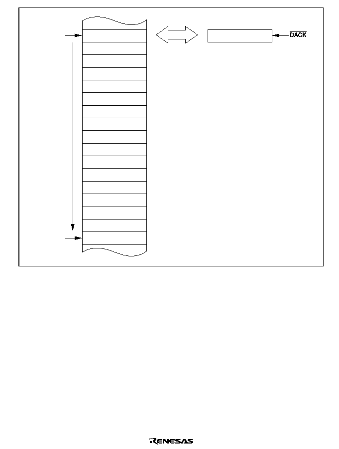
Rev. 2.0, 04/02, page 295 of 906
Address T
Address B
Transfer
1 byte or word transfer performed in
response to 1 transfer request
Legend
Address T = L
Address B = L + (≠1)
DTID
∑ (2
DTSZ
∑ (N ≠ 1))
Where : L = Value set in MAR
N = Value set in ETCR
Figure 7.9 Operation in Single Address Mode (When Sequential Mode is Specified)
Figure 7.10 shows an example of the setting procedure for single address mode (when sequential
mode is specified).
Rev. 2.0, 04/02, page 296 of 906
Single address
mode setting
Set DMABCRH
Set transfer source and
transfer destination
addresses
Set number of transfers
Set DMACR
Read DMABCRL
Set DMABCRL
Single address mode
[1]
[2]
[3]
[4]
[5]
[6]
[1] Set each bit in DMABCRH.
∑ Clear the FAE bit to 0 to select short address
mode.
∑ Set the SAE bit to 1 to select single address
mode.
∑ Specify enabling or disabling of internal
interrupt clearing with the DTA bit.
[2] Set the transfer source address/transfer
destination address in MAR.
[3] Set the number of transfers in ETCR.
[4] Set each bit in DMACR.
∑ Set the transfer data size with the DTSZ bit.
∑ Specify whether MAR is to be incremented or
decremented with the DTID bit.
∑ Clear the RPE bit to 0 to select sequential
mode.
∑ Specify the transfer direction with the DTDIR
bit.
∑ Select the activation source with bits DTF3 to
DTF0.
[5] Read the DTE bit in DMABCRL as 0.
[6] Set each bit in DMABCRL.
∑ Specify enabling or disabling of transfer end
interrupts with the DTIE bit.
∑ Set the DTE bit to 1 to enable transfer.
Figure 7.10 Example of Single Address Mode Setting Procedure (When Sequential Mode is
Specified)
7.5.6
Normal Mode
In normal mode, transfer is performed with channels A and B used in combination. Normal mode
can be specified by setting the FAE bit in DMABCRH to 1 and clearing the BLKE bit in
DMACRA to 0. In normal mode, MAR is updated after data transfer of a byte or word in response

Rev. 2.0, 04/02, page 297 of 906
to a single transfer request, and this is executed the number of times specified in ETCRA. The
transfer source is specified by MARA, and the transfer destination by MARB. Table 7.9
summarizes register functions in normal mode.
Table 7.9
Register Functions in Normal Mode
Register
Function
Initial Setting
Operation
23
0
MARA
Source address
register
Start address of
transfer source
Incremented/decremented
every transfer, or fixed
23
0
MARB
Destination
address register
Start address of
transfer destination
Incremented/decremented
every transfer, or fixed
0
15
ETCRA
Transfer counter
Number of transfers Decremented every
transfer; transfer ends
when count reaches
H'0000
MARA and MARB specify the start addresses of the transfer source and transfer destination,
respectively, as 24 bits. MAR can be incremented or decremented by 1 or 2 each time a byte or
word is transferred, or can be fixed. Incrementing, decrementing, or holding a fixed value can be
set separately for MARA and MARB.
The number of transfers is specified by ETCRA as 16 bits. ETCRA is decremented by 1 each time
a transfer is performed, and when its value reaches H'0000 the DTE bit in DMABCRL is cleared
and transfer ends. If the DTIE bit in DMABCRL is set to 1 at this time, an interrupt request is sent
to the CPU or DTC. The maximum number of transfers, when H'0000 is set in ETCRA, is 65,536.
Figure 7.11 illustrates operation in normal mode.
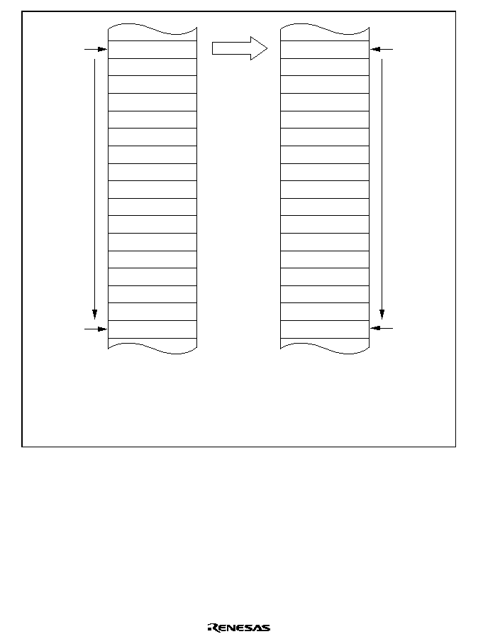
Rev. 2.0, 04/02, page 298 of 906
Address T
A
Address B
A
Transfer
Address T
B
Legend
Address
Address
Address
Address
Where :
Address B
B
= L
A
= L
B
= L
A
+ SAIDE ∑ (≠1)
SAID
∑ (2
DTSZ
∑ (N ≠ 1))
= L
B
+ DAIDE ∑ (≠1)
DAID
∑ (2
DTSZ
∑ (N ≠ 1))
= Value set in MARA
= Value set in MARB
= Value set in ETCRA
T
A
T
B
B
A
B
B
L
A
L
B
N
Figure 7.11 Operation in Normal Mode
Transfer requests (activation sources) are external requests and auto-requests. With auto-request,
the DMAC is only activated by register setting, and the specified number of transfers are
performed automatically. With auto-request, cycle steal mode or burst mode can be selected. In
cycle steal mode, the bus is released to another bus master each time a transfer is performed. In
burst mode, the bus is held continuously until transfer ends.
Figure 7.12 shows an example of the setting procedure for normal mode.
Rev. 2.0, 04/02, page 299 of 906
Normal mode setting
Set DMABCRH
Set transfer source and
transfer destination
addresses
Set number of transfers
Set DMACR
Read DMABCRL
Set DMABCRL
Normal mode
[1]
[2]
[3]
[4]
[5]
[6]
[1] Set each bit in DMABCRH.
∑ Set the FAE bit to 1 to select full address
mode.
∑ Specify enabling or disabling of internal
interrupt clearing with the DTA bit.
[2] Set the transfer source address in MARA, and
the transfer destination address in MARB.
[3] Set the number of transfers in ETCRA.
[4] Set each bit in DMACRA and DMACRB.
∑ Set the transfer data size with the DTSZ bit.
∑ Specify whether MARA is to be incremented,
decremented, or fixed, with the SAID and
SAIDE bits.
∑ Clear the BLKE bit to 0 to select normal
mode.
∑ Specify whether MARB is to be incremented,
decremented, or fixed, with the DAID and
DAIDE bits.
∑ Select the activation source with bits DTF3 to
DTF0.
[5] Read DTE = 0 and DTME = 0 in DMABCRL.
[6] Set each bit in DMABCRL.
∑ Specify enabling or disabling of transfer end
interrupts with the DTIE bit.
∑ Set both the DTME bit and the DTE bit to 1 to
enable transfer.
Figure 7.12 Example of Normal Mode Setting Procedure
7.5.7
Block Transfer Mode
In block transfer mode, data transfer is performed with channels A and B used in combination.
Block transfer mode can be specified by setting the FAE bit in DMABCRH and the BLKE bit in
DMACRA to 1. In block transfer mode, a data transfer of the specified block size is carried out in
response to a single transfer request, and this is executed for the number of times specified in
Rev. 2.0, 04/02, page 300 of 906
ETCRB. The transfer source is specified by MARA, and the transfer destination by MARB. Either
the transfer source or the transfer destination can be selected as a block area (an area composed of
a number of bytes or words). Table 7.10 summarizes register functions in block transfer mode.
Table 7.10
Register Functions in Block Transfer Mode
Register
Function
Initial Setting
Operation
23
0
MARA
Source address
register
Start address of
transfer source
Incremented/decremented
every transfer, or fixed
23
0
MARB
Destination
address register
Start address of
transfer destination
Incremented/decremented
every transfer, or fixed
0
ETCRAH
7
0
ETCRAL
7
Holds block
size
Block size
counter
Block size
Block size
Fixed
Decremented every
transfer; ETCRH value
copied when count
reaches H'00
15
0
ETCRB
Block transfer
counter
Number of block
transfers
Decremented every block
transfer; transfer ends
when count reaches
H'0000
MARA and MARB specify the start addresses of the transfer source and transfer destination,
respectively, as 24 bits. MAR can be incremented or decremented by 1 or 2 each time a byte or
word is transferred, or can be fixed. Incrementing, decrementing, or holding a fixed value can be
set separately for MARA and MARB. Whether a block is to be designated for MARA or for
MARB is specified by the BLKDIR bit in DMACRA.
To specify the number of transfers, if M is the size of one block (where M = 1 to 256) and N
transfers are to be performed (where N = 1 to 65,536), M is set in both ETCRAH and ETCRAL,
and N in ETCRB.
Figure 7.13 illustrates operation in block transfer mode when MARB is designated as a block area.
Rev. 2.0, 04/02, page 301 of 906
Address T
A
Address B
A
Transfer
Address T
B
Address B
B
1st block
2nd block
Nth block
Block area
Consecutive transfer
of M bytes or words
is performed in
response to one
request
Legend
Address
Address
Address
Address
Where :
= L
A
= L
B
= L
A
+ SAIDE ∑ (≠1)
SAID
∑ (2
DTSZ
∑ (M∑N ≠ 1))
= L
B
+ DAIDE ∑ (≠1)
DAID
∑ (2
DTSZ
∑ (N ≠ 1))
= Value set in MARA
= Value set in MARB
= Value set in ETCRB
= Value set in ETCRAH and ETCRAL
T
A
T
B
B
A
B
B
L
A
L
B
N
M
Figure 7.13 Operation in Block Transfer Mode (BLKDIR = 0)
Figure 7.14 illustrates operation in block transfer mode when MARA is designated as a block area.
Rev. 2.0, 04/02, page 302 of 906
Address T
B
Address B
B
Transfer
Address T
A
Address B
A
1st block
2nd block
Nth block
Block area
Consecutive transfer
of M bytes or words
is performed in
response to one
request
Legend
Address
Address
Address
Address
Where :
= L
A
= L
B
= L
A
+ SAIDE ∑ (≠1)
SAID
∑ (2
DTSZ
∑ (N ≠ 1))
= L
B
+ DAIDE ∑ (≠1)
DAID
∑ (2
DTSZ
∑ (M∑N ≠ 1))
= Value set in MARA
= Value set in MARB
= Value set in ETCRB
= Value set in ETCRAH and ETCRAL
T
A
T
B
B
A
B
B
L
A
L
B
N
M
Figure 7.14 Operation in Block Transfer Mode (BLKDIR = 1)
ETCRAL is decremented by 1 each time a byte or word transfer is performed. In response to a
single transfer request, burst transfer is performed until the value in ETCRAL reaches H'00.
ETCRAL is then loaded with the value in ETCRAH. At this time, the value in the MAR register
for which a block designation has been given by the BLKDIR bit in DMACRA is restored in
accordance with the DTSZ, SAID/DAID, and SAIDE/DAIDE bits in DMACR.
ETCRB is decremented by 1 after every block transfer, and when the count reaches H'0000 the
DTE bit in DMABCRL is cleared and transfer ends. If the DTIE bit in DMABCRL is set to 1 at
this point, an interrupt request is sent to the CPU or DTC.

Rev. 2.0, 04/02, page 303 of 906
Figure 7.15 shows the operation flow in block transfer mode.
Acquire bus
ETCRAL = ETCRAL ≠ 1
Transfer request?
ETCRAL = H'00
Release bus
BLKDIR = 0
ETCRAL = ETCRAH
ETCRB = ETCRB ≠ 1
ETCRB = H'0000
Start
(DTE = DTME = 1)
Read address specified by MARA
MARA = MARA + SAIDE∑(≠1)
SAID
∑2
DTSZ
Write to address specified by MARB
MARB = MARB + DAIDE∑(≠1)
DAID
∑2
DTSZ
MARB = MARB ≠ DAIDE∑(≠1)
DAID
∑2
DTSZ
∑ETCRAH
MARA = MARA ≠ SAIDE∑(≠1)
SAID
∑2
DTSZ
∑ETCRAH
No
Yes
No
Yes
No
Yes
No
Yes
Clear DTE bit to 0
to end transfer
Figure 7.15 Operation Flow in Block Transfer Mode
Rev. 2.0, 04/02, page 304 of 906
Transfer requests (activation sources) consist of external requests, SCI transmission complete and
reception complete interrupts, and TPU channel 0 to 5 compare match/input capture A interrupts.
Figure 7.16 shows an example of the setting procedure for block transfer mode.
Block transfer
mode setting
Set DMABCRH
Set transfer source
and transfer destination
addresses
Set number of transfers
Set DMACR
Read DMABCRL
Set DMABCRL
Block transfer mode
[1]
[2]
[3]
[4]
[5]
[6]
[1] Set each bit in DMABCRH.
∑ Set the FAE bit to 1 to select full address
mode.
∑ Specify enabling or disabling of internal
interrupt clearing with the DTA bit.
[2] Set the transfer source address in MARA, and
the transfer destination address in MARB.
[3] Set the block size in both ETCRAH and
ETCRAL. Set the number of transfers in
ETCRB.
[4] Set each bit in DMACRA and DMACRB.
∑ Set the transfer data size with the DTSZ bit.
∑ Specify whether MARA is to be incremented,
decremented, or fixed, with the SAID and
SAIDE bits.
∑ Set the BLKE bit to 1 to select block transfer
mode.
∑ Specify whether the transfer source or the
transfer destination is a block area with the
BLKDIR bit.
∑ Specify whether MARB is to be incremented,
decremented, or fixed, with the DAID and
DAIDE bits.
∑ Select the activation source with bits DTF3 to
DTF0.
[5] Read DTE = 0 and DTME = 0 in DMABCRL.
[6] Set each bit in DMABCRL.
∑ Specify enabling or disabling of transfer end
interrupts to the CPU with the DTIE bit.
∑ Set both the DTME bit and the DTE bit to 1 to
enable transfer.
Figure 7.16 Example of Block Transfer Mode Setting Procedure
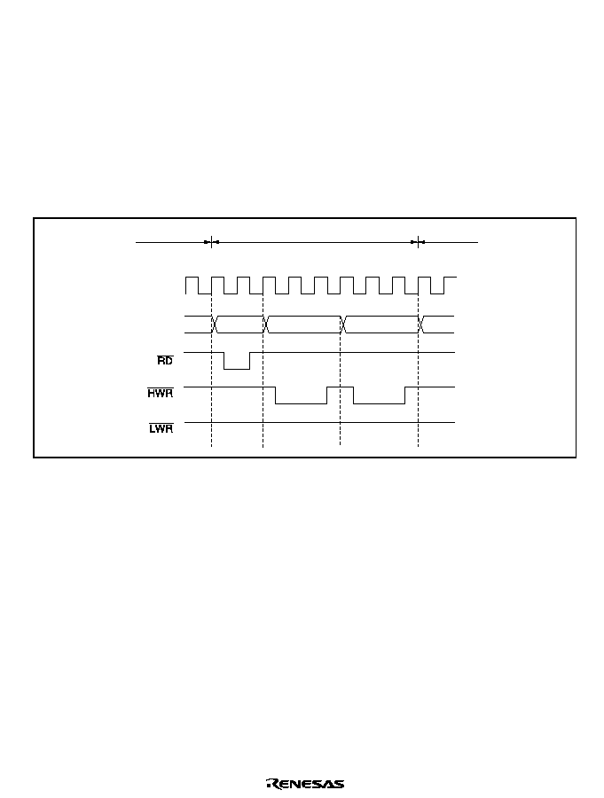
Rev. 2.0, 04/02, page 305 of 906
7.5.8
Basic Bus Cycles
An example of the basic DMAC bus cycle timing is shown in figure 7.17. In this example, word-
size transfer is performed from 16-bit, 2-state access space to 8-bit, 3-state access space. When
the bus is transferred from the CPU to the DMAC, a source address read and destination address
write are performed. The bus is not released in response to another bus request, etc., between
these read and write operations. As like CPU cycles, DMA cycles conform to the bus controller
settings.
The address is not output to the external address bus in an access to on-chip memory or an internal
I/O register.
¯
Address bus
DMAC cycle (1-word transfer)
Source
address
Destination address
CPU cycle
CPU cycle
T
1
T
2
T
3
T
1
T
2
T
3
T
1
T
2
Figure 7.17 Example of DMA Transfer Bus Timing
7.5.9
DMA Bus Cycles (Dual Address Mode)
Short Address Mode: Figure 7.18 shows a transfer example in which
7(1' output is enabled
and byte-size short address mode transfer (sequential/idle/repeat mode) is performed from external
8-bit, 2-state access space to internal I/O space.

Rev. 2.0, 04/02, page 306 of 906
DMA
read
¯
Address bus
Bus release
Last transfer
cycle
DMA
write
DMA
dead
DMA
read
DMA
write
DMA
read
DMA
write
Bus release
Bus release
Bus
release
Figure 7.18 Example of Short Address Mode Transfer
A byte or word transfer is performed for a single transfer request, and after the transfer, the bus is
released. While the bus is released, one or more bus cycles are executed by the CPU or DTC.
In the transfer end cycle (the cycle in which the transfer counter reaches 0), a one-state DMA dead
cycle is inserted after the DMA write cycle.
In repeat mode, when
7(1' output is enabled, 7(1' output goes low in the transfer end cycle.
Full Address Mode (Cycle Steal Mode): Figure 7.19 shows a transfer example in which
7(1'
output is enabled and word-size full address mode transfer (cycle steal mode) is performed from
external 16-bit, 2-state access space to external 16-bit, 2-state access space.
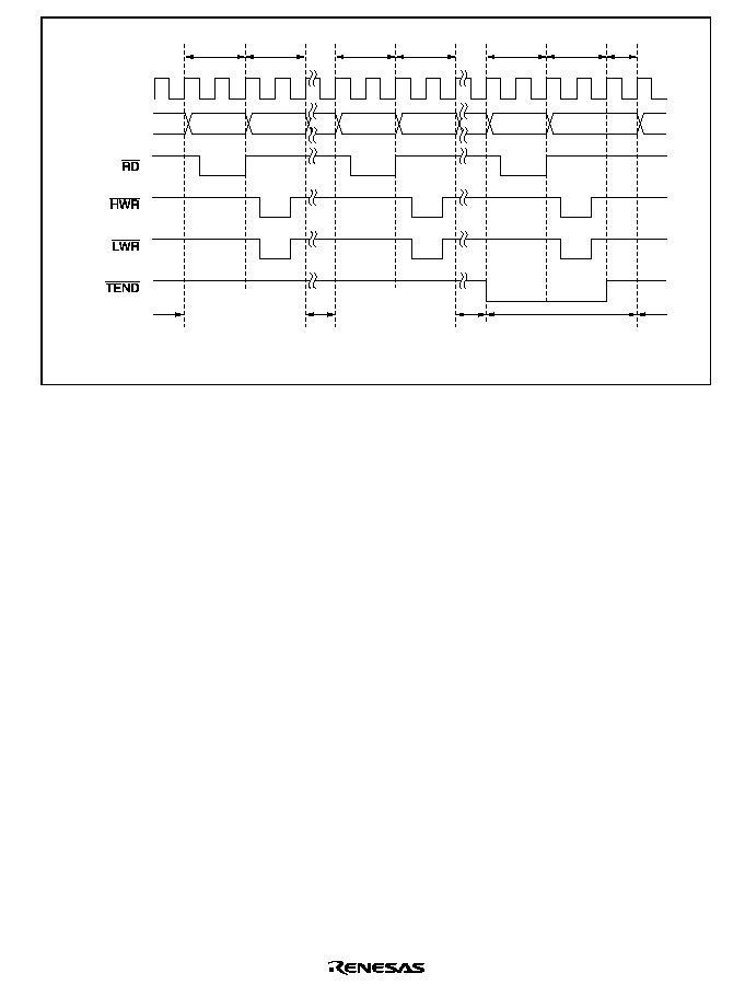
Rev. 2.0, 04/02, page 307 of 906
DMA
read
¯
Address bus
Bus release
Last transfer
cycle
DMA
write
DMA
read
DMA
write
DMA
read
DMA
write
DMA
dead
Bus release
Bus release
Bus
release
Figure 7.19 Example of Full Address Mode Transfer (Cycle Steal)
A byte or word transfer is performed for a single transfer request, and after the transfer, the bus is
released. While the bus is released, one bus cycle is executed by the CPU or DTC.
In the transfer end cycle (the cycle in which the transfer counter reaches 0), a one-state DMA dead
cycle is inserted after the DMA write cycle.
Full Address Mode (Burst Mode): Figure 7.20 shows a transfer example in which
7(1' output
is enabled and word-size full address mode transfer (burst mode) is performed from external 16-
bit, 2-state access space to external 16-bit, 2-state access space.
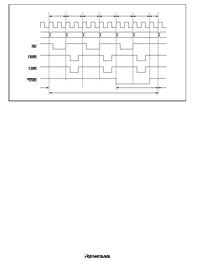
Rev. 2.0, 04/02, page 308 of 906
DMA
read
¯
Address bus
Bus release
DMA
write
DMA
dead
DMA
read
DMA
write
DMA
read
DMA
write
Bus release
Burst transfer
Last transfer cycle
Figure 7.20 Example of Full Address Mode Transfer (Burst Mode)
In burst mode, one-byte or one-word transfers are executed consecutively until transfer ends.
In the transfer end cycle (the cycle in which the transfer counter reaches 0), a one-state DMA dead
cycle is inserted after the DMA write cycle.
If a request from another higher-priority channel is generated after burst transfer starts, that
channel has to wait until the burst transfer ends.
If an NMI interrupt is generated while a channel designated for burst transfer is in the transfer
enabled state, the DTME bit in DMABCRL is cleared and the channel is placed in the transfer
disabled state. If burst transfer has already been activated inside the DMAC, the bus is released on
completion of a one-byte or one-word transfer within the burst transfer, and burst transfer is
suspended. If the last transfer cycle of the burst transfer has already been activated inside the
DMAC, execution continues to the end of the transfer even if the DTME bit is cleared.
Full Address Mode (Block Transfer Mode): Figure 7.21 shows a transfer example in which
7(1' output is enabled and word-size full address mode transfer (block transfer mode) is
performed from internal 16-bit, 1-state access space to external 16-bit, 2-state access space.
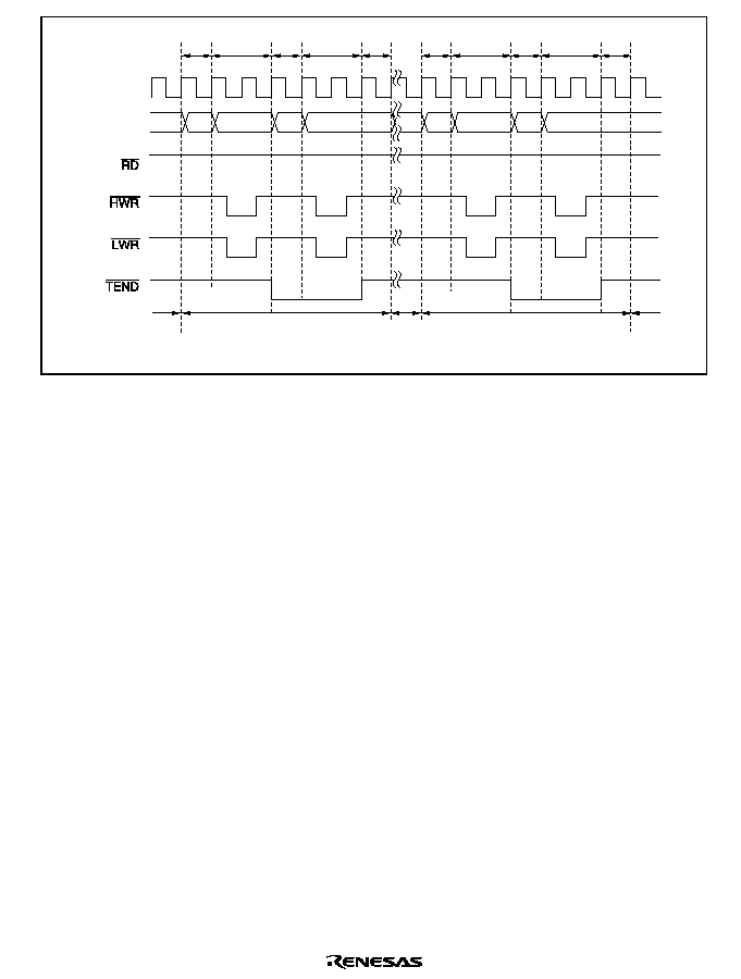
Rev. 2.0, 04/02, page 309 of 906
DMA
read
¯
Address bus
Bus release
Block transfer
Last block transfer
DMA
write
DMA
read
DMA
write
DMA
dead
DMA
read
DMA
write
DMA
read
DMA
write
DMA
dead
Bus
release
Bus release
Figure 7.21 Example of Full Address Mode Transfer (Block Transfer Mode)
A one-block transfer is performed for a single transfer request, and after the transfer the bus is
released. While the bus is released, one or more bus cycles are executed by the CPU or DTC.
In the transfer end cycle of each block (the cycle in which the transfer counter reaches 0), a one-
state DMA dead cycle is inserted after the DMA write cycle. Even if an NMI interrupt is generated
during data transfer, block transfer operation is not affected until data transfer for one block has
ended.
#"
#" Pin Falling Edge Activation Timing: Set the DTA bit in DMABCRH to 1 for the channel
for which the
'5(4 pin is selected.
Figure 7.22 shows an example of normal mode transfer activated by the
'5(4 pin falling edge.
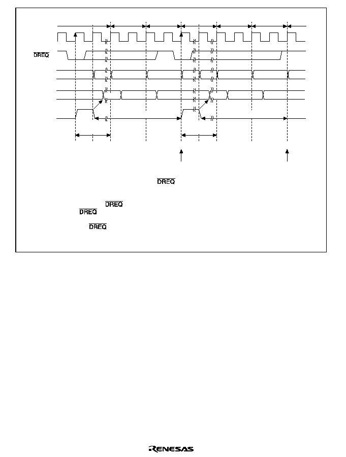
Rev. 2.0, 04/02, page 310 of 906
DMA
read
¯
Address
bus
Idle
Write
Idle
Bus release
DMA
control
Channel
Write
Idle
Transfer source
Request
[1]
[3]
[2]
[4]
[6]
[5]
[7]
Acceptance resumes
Acceptance resumes
DMA
write
Bus
release
DMA
read
DMA
write
Bus
release
Request
Transfer destination
Transfer source
Transfer destination
Read
Read
Request clear period
Request clear period
Minimum
of 2 cycles
Minimum
of 2 cycles
[1]
Acceptance after transfer enabling; the
pin low level is sampled on the rising edge of ¯,
and the request is held.
[2] [5] The request is cleared at the next bus break, and activation is started in the DMAC.
[3] [6] Start of DMA cycle;
pin high level sampling on the rising edge of ¯ starts.
[4] [7] When the
pin high level has been sampled, acceptance is resumed after the write cycle
is completed.
(As in [1], the
pin low level is sampled on the rising edge of ¯, and the request is held.)
Note: In write data buffer mode, bus breaks from [2] to [7] may be hidden, and not visible.
Figure 7.22 Example of
##"
" Pin Falling Edge Activated Normal Mode Transfer
'5(4 pin sampling is performed every cycle, with the rising edge of the next ¯ cycle after the
end of the DMABCR write cycle for setting the transfer enabled state as the starting point.
When the
'5(4 pin low level is sampled while acceptance by means of the '5(4 pin is
possible, the request is held in the DMAC. Then, when activation is initiated in the DMAC, the
request is cleared, and
'5(4 pin high level sampling for edge detection is started. If '5(4 pin
high level sampling has been completed by the time the DMA write cycle ends, acceptance
resumes after the end of the write cycle,
'5(4 pin low level sampling is performed again, and
this operation is repeated until the transfer ends.
Figure 7.23 shows an example of block transfer mode transfer activated by the
'5(4 pin falling
edge.
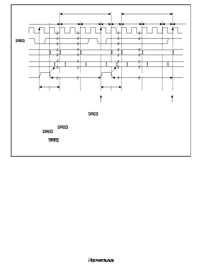
Rev. 2.0, 04/02, page 311 of 906
DMA
read
¯
Address
bus
Idle
Write
Bus release
DMA
control
Channel
Write
Transfer source
Request
[1]
[3]
[2]
[4]
[6]
[5]
[7]
Acceptance resumes
DMA
dead
1 block transfer
Idle
Dead
Dead
DMA
write
Bus
release
DMA
read
DMA
write
DMA
dead
Bus
release
Transfer source
Request
Acceptance resumes
1 block transfer
Transfer destination
Transfer destination
Read
Idle
Read
Minimum
of 2 cycles
Minimum
of 2 cycles
Request clear period
Request clear period
[1]
Acceptance after transfer enabling; the
pin low level is sampled on the rising edge of ¯,
and the request is held.
[2] [5] The request is cleared at the next bus break, and activation is started in the DMAC.
[3] [6] Start of DMA cycle;
pin high level sampling on the rising edge of ¯ starts.
[4] [7] When the
pin high level has been sampled, acceptance is resumed after the dead cycle
is completed.
(As in [1], the
pin low level is sampled on the rising edge of ¯, and the request is held.)
Note: In write data buffer mode, bus breaks from [2] to [7] may be hidden, and not visible.
Figure 7.23 Example of
##"
" Pin Falling Edge Activated Block Transfer Mode Transfer
'5(4 pin sampling is performed every cycle, with the rising edge of the next ¯ cycle after the
end of the DMABCR write cycle for setting the transfer enabled state as the starting point.
When the
'5(4 pin low level is sampled while acceptance by means of the '5(4 pin is
possible, the request is held in the DMAC. Then, when activation is initiated in the DMAC, the
request is cleared, and
'5(4 pin high level sampling for edge detection is started. If '5(4 pin
high level sampling has been completed by the time the DMA dead cycle ends, acceptance
resumes after the end of the dead cycle,
'5(4 pin low level sampling is performed again, and this
operation is repeated until the transfer ends.
#"
#" Pin Low Level Activation Timing (Normal Mode): Set the DTA bit in DMABCRH to 1
for the channel for which the
'5(4 pin is selected.
Figure 7.24 shows an example of normal mode transfer activated by the
'5(4 pin low level.
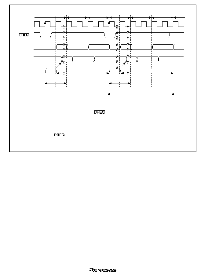
Rev. 2.0, 04/02, page 312 of 906
DMA
read
DMA
write
¯
Address
bus
Idle
Write
Idle
Bus
release
DMA
control
Channel
Write
Idle
Transfer source
Bus
release
DMA
read
DMA
write
Bus
release
Request
[1]
[3]
[2]
[4]
[6]
[5]
[7]
Acceptance resumes
Acceptance resumes
Transfer destination
Transfer source
Transfer destination
Request
Request clear period
Request clear period
Read
Read
Minimum
of 2 cycles
Minimum
of 2 cycles
[1]
Acceptance after transfer enabling; the
pin low level is sampled on the rising edge of ¯,
and the request is held.
[2] [5] The request is cleared at the next bus break, and activation is started in the DMAC.
[3] [6] The DMA cycle is started.
[4] [7] Acceptance is resumed after the write cycle is completed.
(As in [1], the
pin low level is sampled on the rising edge of ¯, and the request is held.)
Note: In write data buffer mode, bus breaks from [2] to [7] may be hidden, and not visible.
Figure 7.24 Example of
##"
" Pin Low Level Activated Normal Mode Transfer
'5(4 pin sampling is performed every cycle, with the rising edge of the next ¯ cycle after the
end of the DMABCR write cycle for setting the transfer enabled state as the starting point.
When the
'5(4 pin low level is sampled while acceptance by means of the '5(4 pin is
possible, the request is held in the DMAC. Then, when activation is initiated in the DMAC, the
request is cleared. After the end of the write cycle, acceptance resumes,
'5(4 pin low level
sampling is performed again, and this operation is repeated until the transfer ends.
Figure 7.25 shows an example of block transfer mode transfer activated by
'5(4 pin low level.
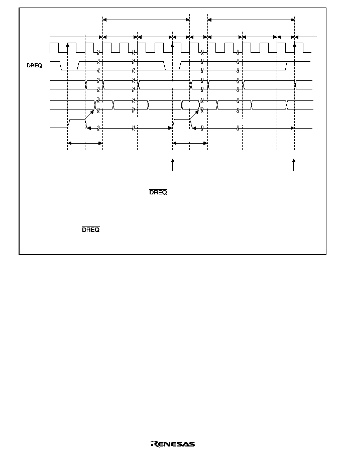
Rev. 2.0, 04/02, page 313 of 906
DMA
read
DMA
write
¯
Address
bus
Idle
Write
Bus release
DMA
control
Channel
Write
Transfer source
Request
[1]
[3]
[2]
[4]
[6]
[5]
[7]
Acceptance resumes
DMA
dead
Bus
release
DMA
read
DMA
write
DMA
dead
Bus
release
1 block transfer
Idle
Dead
Dead
1 block transfer
Acceptance resumes
Request
Minimum
of 2 cycles
Minimum
of 2 cycles
Transfer source
Read
Request clear period
Read
Request clear period
Transfer destination
Transfer destination
Idle
[1]
Acceptance after transfer enabling; the
pin low level is sampled on the rising edge of ¯,
and the request is held.
[2] [5] The request is cleared at the next bus break, and activation is started in the DMAC.
[3] [6] The DMA cycle is started.
[4] [7] Acceptance is resumed after the dead cycle is completed.
(As in [1], the
pin low level is sampled on the rising edge of ¯, and the request is held.)
Note: In write data buffer mode, bus breaks from [2] to [7] may be hidden, and not visible.
Figure 7.25 Example of
##"
" Pin Low Level Activated Block Transfer Mode Transfer
'5(4 pin sampling is performed every cycle, with the rising edge of the next ¯ cycle after the
end of the DMABCR write cycle for setting the transfer enabled state as the starting point.
When the
'5(4 pin low level is sampled while acceptance by means of the '5(4 pin is
possible, the request is held in the DMAC. Then, when activation is initiated in the DMAC, the
request is cleared. After the end of the dead cycle, acceptance resumes,
'5(4 pin low level
sampling is performed again, and this operation is repeated until the transfer ends.
7.5.10
DMA Bus Cycles (Single Address Mode)
Single Address Mode (Read): Figure 7.26 shows a transfer example in which
7(1' output is
enabled and byte-size single address mode transfer (read) is performed from external 8-bit, 2-state
access space to an external device.
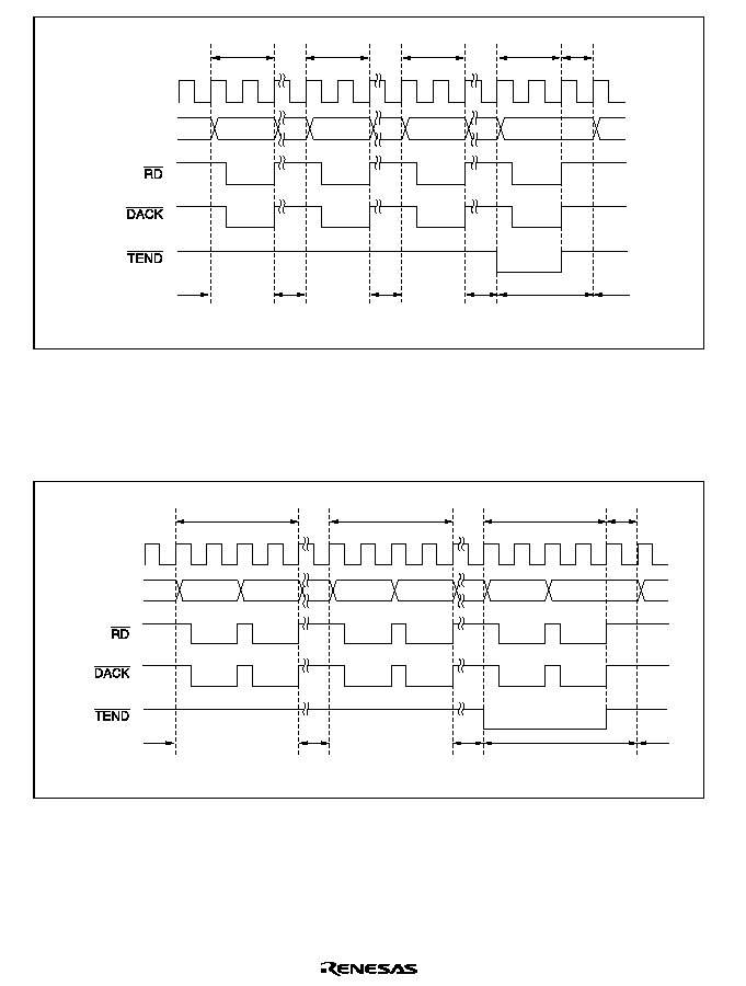
Rev. 2.0, 04/02, page 314 of 906
DMA read
¯
Address bus
DMA
dead
Bus
release
DMA read
DMA read
DMA read
Bus
release
Bus
release
Bus
release
Bus
release
Last transfer
cycle
Figure 7.26 Example of Single Address Mode Transfer (Byte Read)
Figure 7.27 shows a transfer example in which
7(1' output is enabled and word-size single
address mode transfer (read) is performed from external 8-bit, 2-state access space to an external
device.
DMA read
¯
Address bus
DMA read
DMA read
DMA
dead
Bus
release
Bus
release
Bus
release
Bus
release
Last transfer
cycle
Figure 7.27 Example of Single Address Mode (Word Read) Transfer
A byte or word transfer is performed for a single transfer request, and after the transfer, the bus is
released. While the bus is released, one or more bus cycles are executed by the CPU or DTC.
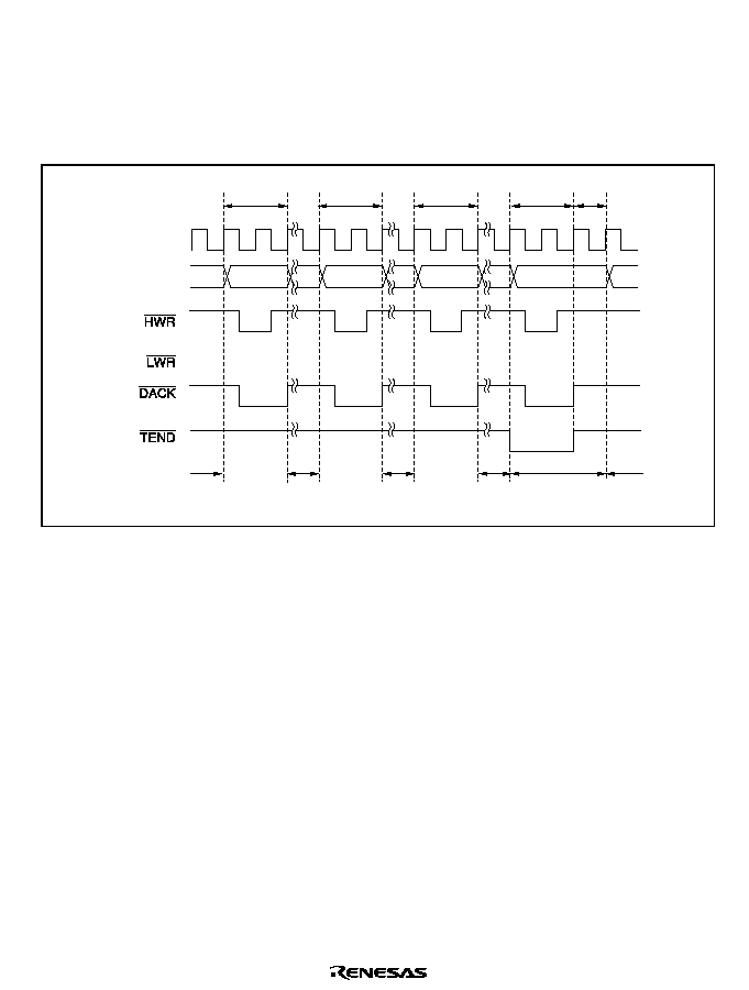
Rev. 2.0, 04/02, page 315 of 906
In the transfer end cycle (the cycle in which the transfer counter reaches 0), a one-state DMA dead
cycle is inserted after the DMA write cycle.
Single Address Mode (Write): Figure 7.28 shows a transfer example in which
7(1' output is
enabled and byte-size single address mode transfer (write) is performed from an external device to
external 8-bit, 2-state access space.
DMA write
¯
Address bus
DMA
dead
Bus
release
DMA write
DMA write
DMA write
Bus
release
Bus
release
Bus
release
Bus
release
Last transfer
cycle
Figure 7.28 Example of Single Address Mode Transfer (Byte Write)
Figure 7.29 shows a transfer example in which
7(1' output is enabled and word-size single
address mode transfer (write) is performed from an external device to external 8-bit, 2-state access
space.
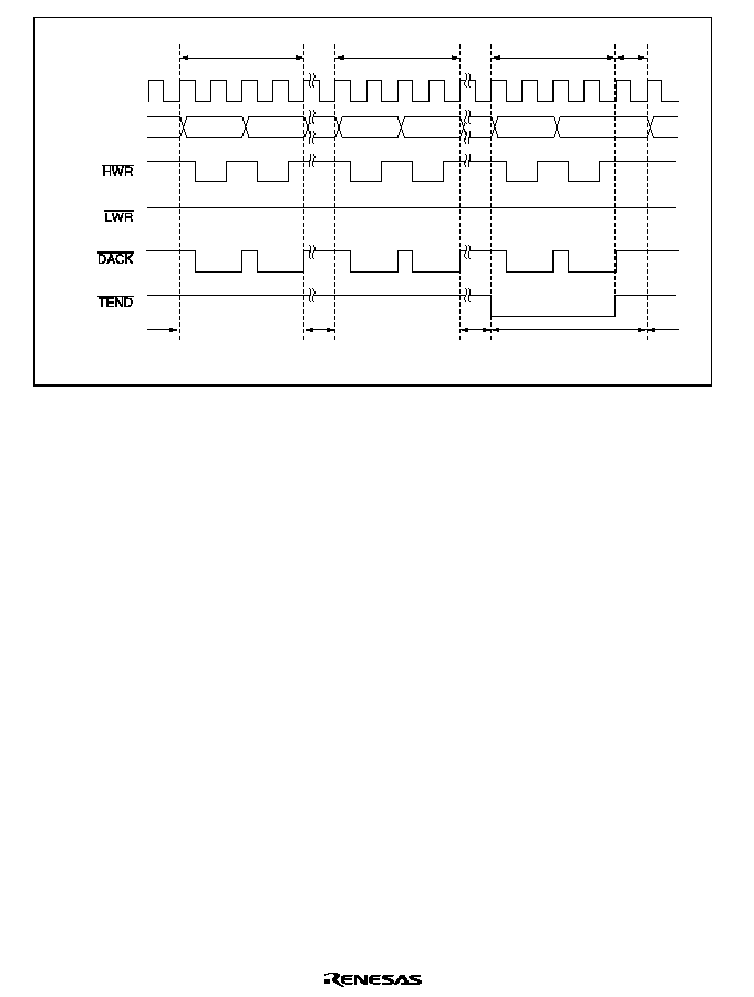
Rev. 2.0, 04/02, page 316 of 906
DMA write
¯
Address bus
DMA write
DMA write
DMA
dead
Bus
release
Bus
release
Bus
release
Bus
release
Last transfer
cycle
Figure 7.29 Example of Single Address Mode Transfer (Word Write)
A byte or word transfer is performed for a single transfer request, and after the transfer, the bus is
released. While the bus is released, one or more bus cycles are executed by the CPU or DTC.
In the transfer end cycle (the cycle in which the transfer counter reaches 0), a one-state DMA dead
cycle is inserted after the DMA write cycle.
#"
#" Pin Falling Edge Activation Timing: Set the DTA bit in DMABCRH to 1 for the channel
for which the
'5(4 pin is selected.
Figure 7.30 shows an example of single address mode transfer activated by the
'5(4 pin falling
edge.
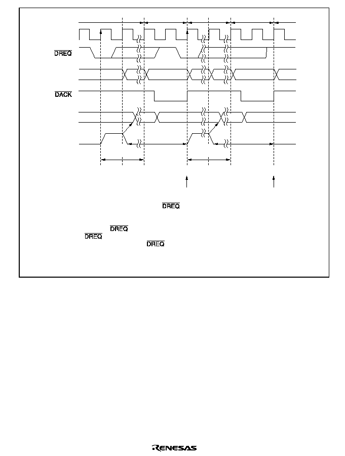
Rev. 2.0, 04/02, page 317 of 906
¯
Bus release
DMA single
DMA single
Address bus
DMA control
Channel
[2]
Transfer source/
destination
Idle
Idle
Idle
[1]
[3]
[5]
[4]
[6]
[7]
Acceptance resumes
Acceptance resumes
Bus release
Bus release
Transfer source/
destination
Request
Request
Request clear
period
Request clear
period
Minimum of
2 cycles
Minimum of
2 cycles
Single
Single
[1]
Acceptance after transfer enabling; the
pin low level is sampled on the rising edge of ¯,
and the request is held.
[2] [5] The request is cleared at the next bus break, and activation is started in the DMAC.
[3] [6] Start of DMA cycle;
pin high level sampling on the rising edge of ¯ starts.
[4] [7] When the
pin high level has been sampled, acceptance is resumed after the single
cycle is completed. (As in [1], the
pin low level is sampled on the rising edge of ¯, and
the request is held.)
Note: In write data buffer mode, bus breaks from [2] to [7] may be hidden, and not visible.
Figure 7.30 Example of
##"
" Pin Falling Edge Activated Single Address Mode Transfer
'5(4 pin sampling is performed every cycle, with the rising edge of the next ¯ cycle after the
end of the DMABCR write cycle for setting the transfer enabled state as the starting point.
When the
'5(4 pin low level is sampled while acceptance by means of the '5(4 pin is
possible, the request is held in the DMAC. Then, when activation is initiated in the DMAC, the
request is cleared, and
'5(4 pin high level sampling for edge detection is started. If '5(4 pin
high level sampling has been completed by the time the DMA single cycle ends, acceptance
resumes after the end of the single cycle,
'5(4 pin low level sampling is performed again, and
this operation is repeated until the transfer ends.
#"
#" Pin Low Level Activation Timing: Set the DTA bit in DMABCRH to 1 for the channel
for which the
'5(4 pin is selected.
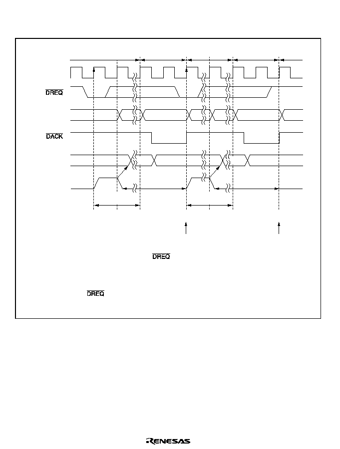
Rev. 2.0, 04/02, page 318 of 906
Figure 7.31 shows an example of single address mode transfer activated by the
'5(4 pin low
level.
¯
Bus release
DMA single
Address bus
DMA control
Channel
[2]
Transfer source/
destination
Idle
Idle
Idle
[1]
[3]
[5]
[4]
[6]
[7]
Acceptance resumes
Acceptance resumes
Bus release
DMA single
Bus
release
Transfer source/
destination
Request
Request
Request clear
period
Request clear
period
Single
Single
Minimum of
2 cycles
Minimum of
2 cycles
[1]
Acceptance after transfer enabling; the
pin low level is sampled on the rising edge of ¯,
and the request is held.
[2] [5] The request is cleared at the next bus break, and activation is started in the DMAC.
[3] [6] The DMAC cycle is started.
[4] [7] Acceptance is resumed after the single cycle is completed.
(As in [1], the
pin low level is sampled on the rising edge of ¯, and the request is held.)
Note: In write data buffer mode, bus breaks from [2] to [7] may be hidden, and not visible.
Figure 7.31 Example of
##"
" Pin Low Level Activated Single Address Mode Transfer
'5(4 pin sampling is performed every cycle, with the rising edge of the next ¯ cycle after the
end of the DMABCR write cycle for setting the transfer enabled state as the starting point.
When the
'5(4 pin low level is sampled while acceptance by means of the '5(4 pin is
possible, the request is held in the DMAC. Then, when activation is initiated in the DMAC, the
request is cleared. After the end of the single cycle, acceptance resumes,
'5(4 pin low level
sampling is performed again, and this operation is repeated until the transfer ends.
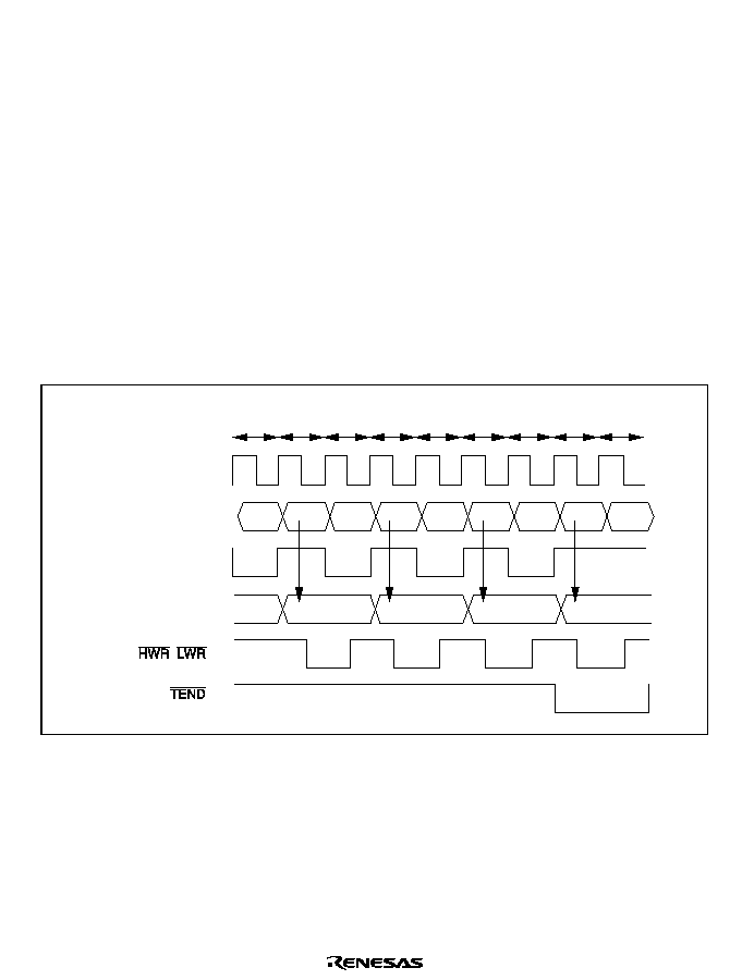
Rev. 2.0, 04/02, page 319 of 906
7.5.11
Write Data Buffer Function
DMAC internal-to-external dual address transfers and single address transfers can be executed at
high speed using the write data buffer function, enabling system throughput to be improved.
When the WDBE bit of BCR in the bus controller is set to 1, enabling the write data buffer
function, dual address transfer external write cycles or single address transfers and internal
accesses (on-chip memory or internal I/O registers) are executed in parallel. Internal accesses are
independent of the bus master, and DMAC dead cycles are regarded as internal accesses.
A low level can always be output from the
7(1' pin if the bus cycle in which a low level is to be
output from the
7(1' pin is an external bus cycle. However, a low level is not output from the
7(1' pin if the bus cycle in which a low level is to be output from the 7(1' pin is an internal
bus cycle, and an external write cycle is executed in parallel with this cycle.
Figure 7.32 shows an example of burst mode transfer from on-chip RAM to external memory
using the write data buffer function.
¯
Internal address
Internal read signal
,
External address
DMA
read
DMA
write
DMA
read
DMA
write
DMA
read
DMA
write
DMA
read
DMA
write
DMA
dead
Figure 7.32 Example of Dual Address Transfer Using Write Data Buffer Function
Figure 7.33 shows an example of single address transfer using the write data buffer function. In
this example, the CPU program area is in on-chip memory.
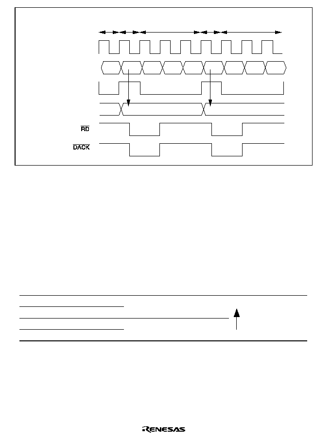
Rev. 2.0, 04/02, page 320 of 906
¯
Internal address
Internal read signal
External address
DMA
read
DMA
single
CPU
read
DMA
single
CPU
read
Figure 7.33 Example of Single Address Transfer Using Write Data Buffer Function
When the write data buffer function is activated, the DMAC recognizes that the bus cycle
concerned has ended, and starts the next operation. Therefore,
'5(4 pin sampling is started one
state after the start of the DMA write cycle or single address transfer.
7.5.12
Multi-Channel Operation
The DMAC channel priority order is: channel 0 > channel 1, and channel A > channel B. Table
7.11 summarizes the priority order for DMAC channels.
Table 7.11
DMAC Channel Priority Order
Short Address Mode
Full Address Mode
Priority
Channel 0A
Channel 0
High
Channel 0B
Channel 1A
Channel 1
Channel 1B
Low
If transfer requests are issued simultaneously for more than one channel, or if a transfer request for
another channel is issued during a transfer, when the bus is released, the DMAC selects the
highest-priority channel from among those issuing a request according to the priority order shown
in table 7.11. During burst transfer, or when one block is being transferred in block transfer, the
channel will not be changed until the end of the transfer. Figure 7.34 shows a transfer example in
which transfer requests are issued simultaneously for channels 0A, 0B, and 1.
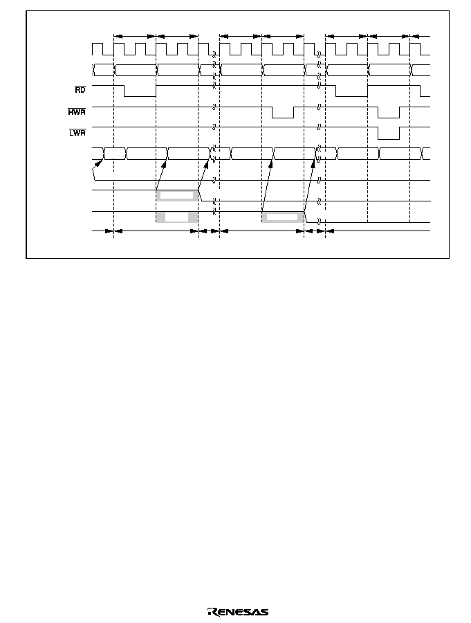
Rev. 2.0, 04/02, page 321 of 906
DMA read
DMA write
DMA read
DMA write
DMA read
DMA write
DMA
read
¯
Address bus
DMA control
Channel 0A
Channel 0B
Channel 1
Idle
Write
Idle
Read
Write
Idle
Read
Write
Read
Request
hold
Request
hold
Bus
release
Channel 0A
transfer
Bus
release
Channel 0B
transfer
Channel 1 transfer
Bus
release
Request
hold
Read
Selection
Non-
selection
Selection
Request clear
Request clear
Request clear
Figure 7.34 Example of Multi-Channel Transfer
7.5.13
Relation between DMAC and External Bus Requests, Refresh Cycles,
and EXDMAC
When the DMAC accesses external space, contention with a refresh cycle, EXDMAC cycle, or
external bus release cycle may arise. In this case, the bus controller will suspend the transfer and
insert a refresh cycle, EXDMAC cycle, or external bus release cycle, in accordance with the
external bus priority order, even if the DMAC is executing a burst transfer or block transfer. (An
external access by the DTC or CPU, which has a lower priority than the DMAC, is not executed
until the DMAC releases the external bus.)
When the DMAC transfer mode is dual address mode, the DMAC releases the external bus after
an external write cycle. The external read cycle and external write cycle are inseparable, and so the
bus cannot be released between these two cycles.
When the DMAC accesses internal space (on-chip memory or an internal I/O register), the DMAC
cycle may be executed at the same time as a refresh cycle, EXDMAC cycle, or external bus
release cycle.
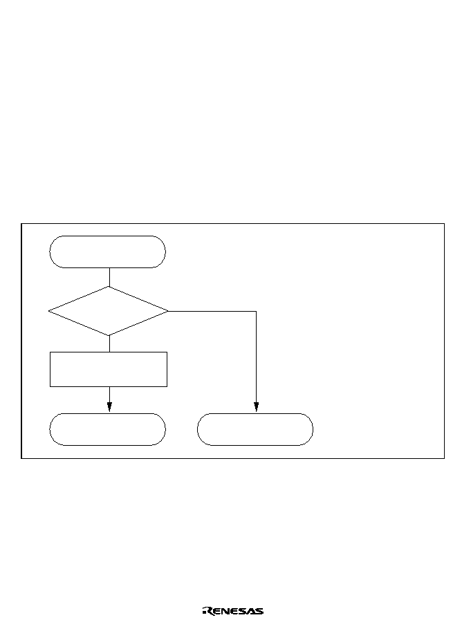
Rev. 2.0, 04/02, page 322 of 906
7.5.14
DMAC and NMI Interrupts
When an NMI interrupt is requested, burst mode transfer in full address mode is interrupted. An
NMI interrupt does not affect the operation of the DMAC in other modes.
In full address mode, transfer is enabled for a channel when both the DTE bit and DTME bit are
set to 1. With burst mode setting, the DTME bit is cleared when an NMI interrupt is requested.
If the DTME bit is cleared during burst mode transfer, the DMAC discontinues transfer on
completion of the 1-byte or 1-word transfer in progress, then releases the bus, which passes to the
CPU.
The channel on which transfer was interrupted can be restarted by setting the DTME bit to 1 again.
Figure 7.35 shows the procedure for continuing transfer when it has been interrupted by an NMI
interrupt on a channel designated for burst mode transfer.
Resumption of
transfer on interrupted
channel
Set DTME bit to 1
Transfer continues
[1]
[2]
DTE = 1
DTME = 0
Transfer ends
No
Yes
[1]
[2]
Check that DTE = 1 and
DTME = 0 in DMABCRL.
Write 1 to the DTME bit.
Figure 7.35 Example of Procedure for Continuing Transfer on Channel Interrupted by
NMI Interrupt
7.5.15
Forced Termination of DMAC Operation
If the DTE bit in DMABCRL is cleared to 0 for the channel currently operating, the DMAC stops
on completion of the 1-byte or 1-word transfer in progress. DMAC operation resumes when the
DTE bit is set to 1 again. In full address mode, the same applies to the DTME bit in DMABCRL.
Figure 7.36 shows the procedure for forcibly terminating DMAC operation by software.
Rev. 2.0, 04/02, page 323 of 906
Forced termination
of DMAC
Clear DTE bit to 0
Forced termination
[1]
[1]
Clear the DTE bit in DMABCRL to 0.
To prevent interrupt generation after forced
termination of DMAC operation, clear the DTIE bit
to 0 at the same time.
Figure 7.36 Example of Procedure for Forcibly Terminating DMAC Operation
7.5.16
Clearing Full Address Mode
Figure 7.37 shows the procedure for releasing and initializing a channel designated for full address
mode. After full address mode has been cleared, the channel can be set to another transfer mode
using the appropriate setting procedure.
Rev. 2.0, 04/02, page 324 of 906
Clearing full
address mode
Stop the channel
Initialize DMACR
Clear FAE bit to 0
Initialization;
operation halted
[1]
[2]
[3]
[1] Clear both the DTE bit and DTME bit in
DMABCRL to 0, or wait until the transfer ends
and the DTE bit is cleared to 0, then clear the
DTME bit to 0. Also clear the corresponding
DTIE bit to 0 at the same time.
[2] Clear all bits in DMACRA and DMACRB to 0.
[3] Clear the FAE bit in DMABCRH to 0.
Figure 7.37 Example of Procedure for Clearing Full Address Mode
7.6
Interrupt Sources
The sources of interrupts generated by the DMAC are transfer end and transfer break. Table 7.12
shows the interrupt sources and their priority order.
Table 7.12
Interrupt Sources and Priority Order
Interrupt
Interrupt Source
Interrupt
Name
Short Address Mode
Full Address Mode
Priority Order
DMTEND0A
Interrupt due to end of
transfer on channel 0A
Interrupt due to end of
transfer on channel 0
High
DMTEND0B
Interrupt due to end of
transfer on channel 0B
Interrupt due to break in
transfer on channel 0
DMTEND1A
Interrupt due to end of
transfer on channel 1A
Interrupt due to end of
transfer on channel 1
DMTEND1B
Interrupt due to end of
transfer on channel 1B
Interrupt due to break in
transfer on channel 1
Low
Rev. 2.0, 04/02, page 325 of 906
Enabling or disabling of each interrupt source is set by means of the DTIE bit in DMABCRL for
the corresponding channel in DMABCRL, and interrupts from each source are sent to the interrupt
controller independently. The priority of transfer end interrupts on each channel is decided by the
interrupt controller, as shown in table 7.12.
Figure 7.38 shows a block diagram of a transfer end/transfer break interrupt. An interrupt is
always generated when the DTIE bit is set to 1 while the DTE bit in DMABCRL is cleared to 0.
DTE/
DTME
DTIE
Transfer end/transfer
break interrupt
Figure 7.38 Block Diagram of Transfer End/Transfer Break Interrupt
In full address mode, a transfer break interrupt is generated when the DTME bit is cleared to 0
while the DTIEB bit is set to 1. In both short address mode and full address mode, DMABCR
should be set so as to prevent the occurrence of a combination that constitutes a condition for
interrupt generation during setting.
7.7
Usage Notes
7.7.1
DMAC Register Access during Operation
Except for forced termination of the DMAC, the operating (including transfer waiting state)
channel setting should not be changed. The operating channel setting should only be changed
when transfer is disabled. Also, DMAC registers should not be written to in a DMA transfer.
DMAC register reads during operation (including the transfer waiting state) are described below.
∑
DMAC control starts one cycle before the bus cycle, with output of the internal address.
Consequently, MAR is updated in the bus cycle before DMA transfer. Figure 7.39 shows an
example of the update timing for DMAC registers in dual address transfer mode.
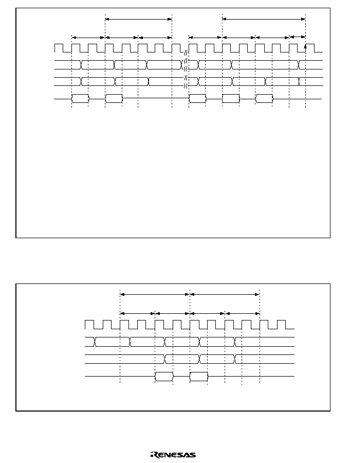
Rev. 2.0, 04/02, page 326 of 906
[1] Transfer source address register MAR operation (incremented/decremented/fixed)
Transfer counter ETCR operation (decremented)
Block size counter ETCR operation (decremented in block transfer mode)
[2] Transfer destination address register MAR operation (incremented/decremented/fixed)
[2']Transfer destination address register MAR operation (incremented/decremented/fixed)
Block transfer counter ETCR operation (decremented, in last transfer cycle of
a block in block transfer mode)
[3] Transfer address register MAR restore operation (in block or repeat transfer mode)
Transfer counter ETCR restore (in repeat transfer mode)
Block size counter ETCR restore (in block transfer mode)
Note: In single address transfer mode, the update timing is the same as [1].
The MAR operation is post-incrementing/decrementing of the DMA internal address value.
[3]
[2']
[2]
[1]
[1]
DMA transfer cycle
DMA read
DMA read
DMA write
DMA write
DMA
dead
DMA Internal
address
DMA control
DMA register
operation
DMA last transfer cycle
Transfer
destination
Transfer
destination
Transfer
source
Transfer
source
Idle
Idle
Idle
Read
Read
Dead
Write
Write
¯
Figure 7.39 DMAC Register Update Timing
∑
If a DMAC transfer cycle occurs immediately after a DMAC register read cycle, the DMAC
register is read as shown in figure 7.40.
[2]
[1]
Note: The lower word of MAR is the updated value after the operation in [1].
CPU longword read
DMA transfer cycle
MAR upper
word read
MAR lower
word read
DMA read
DMA write
DMA internal
address
DMA control
DMA register
operation
Transfe
source
Transfer
destination
Idle
¯
Read
Write
Idle
Figure 7.40 Contention between DMAC Register Update and CPU Read

Rev. 2.0, 04/02, page 327 of 906
7.7.2
Module Stop
When the MSTP13 bit in MSTPCRH is set to 1, the DMAC clock stops, and the module stop state
is entered. However, 1 cannot be written to the MSTP13 bit if any of the DMAC channels is
enabled. This setting should therefore be made when DMAC operation is stopped.
When the DMAC clock stops, DMAC register accesses can no longer be made. Since the
following DMAC register settings are valid even in the module stop state, they should be
invalidated, if necessary, before a module stop.
∑
Transfer end/break interrupt (DTE = 0 and DTIE = 1)
∑
7(1' pin enable (TEE = 1)
∑
'$&. pin enable (FAE = 0 and SAE = 1)
7.7.3
Write Data Buffer Function
When the WDBE bit of BCR in the bus controller is set to 1, enabling the write data buffer
function, dual address transfer external write cycles or single address transfers and internal
accesses (on-chip memory or internal I/O registers) are executed in parallel.
∑
Write data buffer function and DMAC register setting
If the setting of a register that controls external accesses is changed during execution of an
external access by means of the write data buffer function, the external access may not be
performed normally. Registers that control external accesses should only be manipulated when
external reads, etc., are used with DMAC operation disabled, and the operation is not
performed in parallel with external access.
∑
Write data buffer function and DMAC operation timing
The DMAC can start its next operation during external access using the write data buffer
function. Consequently, the
'5(4 pin sampling timing, 7(1' output timing, etc., are
different from the case in which the write data buffer function is disabled. Also, internal bus
cycles maybe hidden, and not visible.
7.7.4
%
% Output
If the last transfer cycle is for an internal address, note that even if low-level output at the
7(1'
pin has been set, a low level may not be output at the
7(1' pin under the following external bus
conditions since the last transfer cycle (internal bus cycle) and the external bus cycle are executed
in parallel.
1. EXDMAC cycle
2. Write cycle with write buffer mode enabled
3. DMAC single address cycle for a different channel with write buffer mode enabled
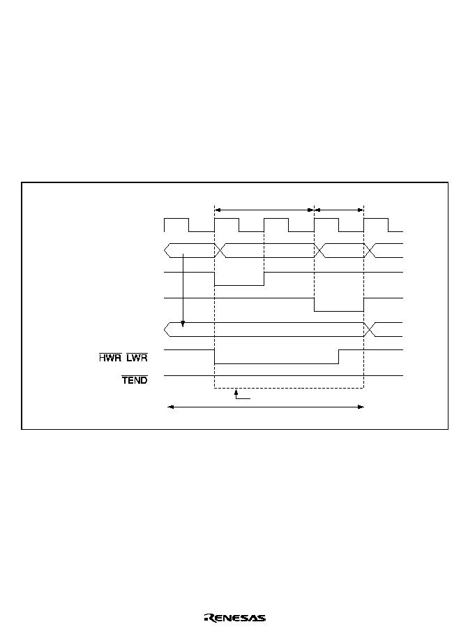
Rev. 2.0, 04/02, page 328 of 906
4. Bus release cycle
5. CBR refresh cycle
Figure 7.41 shows an example in which a low level is not output from the
7(1' pin in case 2
above.
If the last transfer cycle is an external address cycle, a low level is output at the
7(1' pin in
synchronization with the bus cycle.
However, if the last transfer cycle and a CBR refresh occur simultaneously, note that although the
CBR refresh and the last transfer cycle may be executed consecutively,
7(1' may also go low in
this case for the refresh cycle.
¯
Internal address
Internal read signal
External address
,
Internal write signal
Not output
DMA
read
External write by CPU, etc.
DMA
write
Figure 7.41 Example in Which Low Level is Not Output at
%
%
Pin
7.7.5
Activation by Falling Edge on
#"
#" Pin
'5(4 pin falling edge detection is performed in synchronization with DMAC internal operations.
The operation is as follows:
[1] Activation request wait state: Waits for detection of a low level on the
'5(4 pin, and
switches to [2].
[2] Transfer wait state: Waits for DMAC data transfer to become possible, and switches to [3].
[3] Activation request disabled state: Waits for detection of a high level on the
'5(4 pin, and
switches to [1].

Rev. 2.0, 04/02, page 329 of 906
After DMAC transfer is enabled, a transition is made to [1]. Thus, initial activation after transfer
is enabled is performed on detection of a low level.
7.7.6
Activation Source Acceptance
At the start of activation source acceptance, a low level is detected in both
'5(4 pin falling edge
sensing and low level sensing. Similarly, in the case of an internal interrupt, the interrupt request
is detected. Therefore, a request is accepted from an internal interrupt or
'5(4 pin low level that
occurs before write to DMABCRL to enable transfer.
When the DMAC is activated, take any necessary steps to prevent an internal interrupt or
'5(4
pin low level remaining from the end of the previous transfer, etc.
7.7.7
Internal Interrupt after End of Transfer
When the DTE bit in DMABCRL is cleared to 0 at the end of a transfer or by a forcible
termination, the selected internal interrupt request will be sent to the CPU or DTC even if the
DTA bit in DMABCRH is set to 1.
Also, if internal DMAC activation has already been initiated when operation is forcibly
terminated, the transfer is executed but flag clearing is not performed for the selected internal
interrupt even if the DTA bit is set to 1.
An internal interrupt request following the end of transfer or a forcible termination should be
handled by the CPU as necessary.
7.7.8
Channel Re-Setting
To reactivate a number of channels when multiple channels are enabled, use exclusive handling of
transfer end interrupts, and perform DMABCR control bit operations exclusively.
Note, in particular, that in cases where multiple interrupts are generated between reading and
writing of DMABCR, and a DMABCR operation is performed during new interrupt handling, the
DMABCR write data in the original interrupt handling routine will be incorrect, and the write may
invalidate the results of the operations by the multiple interrupts. Ensure that overlapping
DMABCR operations are not performed by multiple interrupts, and that there is no separation
between read and write operations by the use of a bit-manipulation instruction.
Also, when the DTE and DTME bits are cleared by the DMAC or are written with 0, they must
first be read while cleared to 0 before the CPU can write 1 to them.

Rev. 2.0, 04/02, page 330 of 906

Rev. 2.0, 04/02, page 331 of 906
Section 8 EXDMA Controller
This LSI has a built-in four-channel external bus transfer DMA controller (EXDMAC). The
EXDMAC can carry out high-speed data transfer, in place of the CPU, to and from external
devices and external memory with a DACK (DMA transfer notification) facility.
8.1
Features
∑
Direct specification of 16-Mbyte address space
∑
Selection of byte or word transfer data length
∑
Maximum number of transfers: 16M (16,777,215)/infinite (free-running)
∑
Selection of dual address mode or single address mode
∑
Selection of cycle steal mode or burst mode as bus mode
∑
Selection of normal mode or block transfer mode as transfer mode
∑
Two kinds of transfer requests: external request and auto-request
∑
An interrupt request can be sent to the CPU at the end of the specified number of transfers.
∑
Repeat area designation function:
∑
Operation in parallel with internal bus master:
∑
Acceptance of a transfer request and the start of transfer processing can be reported to an
external device via the
('5$. pin.
∑
Module stop mode can be set.
Figure 8.1 shows a block diagram of the EXDMAC.
EDMA260A_010020020400
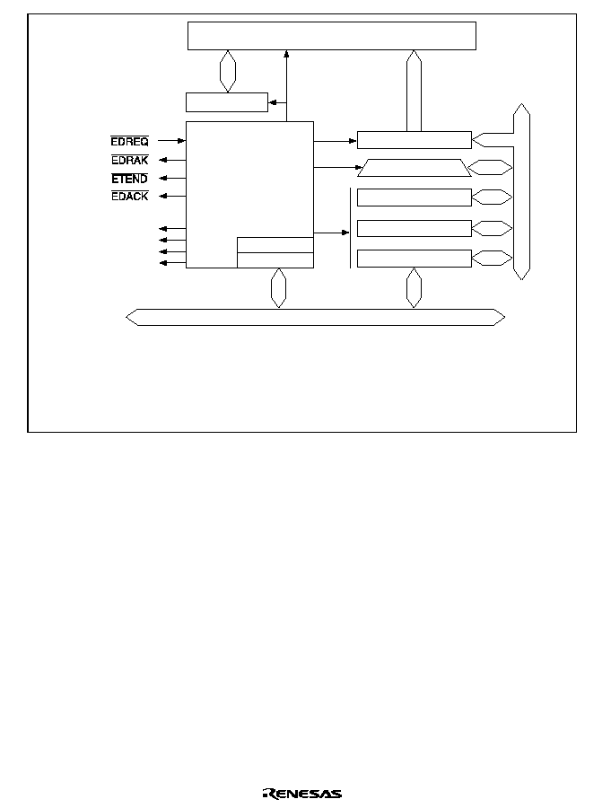
Rev. 2.0, 04/02, page 332 of 906
Bus controller
Internal data bus
Interrupt request
signals to CPU
for individual
channels
External pins
EDMDR
EDACR
EDTCR
EDDAR
EDSAR
Processor
Address buffer
Data buffer
Control logic
Module data bus
Legend
EDSAR:
EXDMA source address register
EDDAR:
EXDMA destination address register
EDTCR:
EXDMA transfer count register
EDMDR:
EXDMA mode control register
EDACR:
EXDMA address control register
Figure 8.1 Block Diagram of EXDMAC

Rev. 2.0, 04/02, page 333 of 906
8.2
Input/Output Pins
Table 8.1 shows the EXDMAC pin configuration.
Table 8.1
Pin Configuration
Channel
Name
Abbre-
viation
I/O
Function
0
EXDMA transfer request 0
('5(4
Input
Channel 0 external request
EXDMA transfer
acknowledge 0
('$&.
Output
Channel 0 single address transfer
acknowledge
EXDMA transfer end 0
(7(1'
Output
Channel 0 transfer end
('5(4
acceptance
acknowledge
('5$.
Output
Notification to external device of
channel 0 external request
acceptance and start of execution
1
EXDMA transfer request 1
('5(4
Input
Channel 1 external request
EXDMA transfer
acknowledge 1
('$&.
Output
Channel 1 single address transfer
acknowledge
EXDMA transfer end 1
(7(1'
Output
Channel 1 transfer end
('5(4
acceptance
acknowledge
('5$.
Output
Notification to external device of
channel 1 external request
acceptance and start of execution
2
EXDMA transfer request 2
('5(4
Input
Channel 2 external request
EXDMA transfer
acknowledge 2
('$&.
Output
Channel 2 single address transfer
acknowledge
EXDMA transfer end 2
(7(1'
Output
Channel 2 transfer end
('5(4
acceptance
acknowledge
('5$.
Output
Notification to external device of
channel 2 external request
acceptance and start of execution
3
EXDMA transfer request 3
('5(4
Input
Channel 3 external request
EXDMA transfer
acknowledge 3
('$&.
Output
Channel 3 single address transfer
acknowledge
EXDMA transfer end 3
(7(1'
Output
Channel 3 transfer end
('5(4
acceptance
acknowledge
('5$.
Output
Notification to external device of
channel 3 external request
acceptance and start of execution

Rev. 2.0, 04/02, page 334 of 906
8.3
Register Descriptions
The EXDMAC has the following registers.
∑
EXDMA source address register_0 (EDSAR_0)
∑
EXDMA destination address register_0 (EDDAR_0)
∑
EXDMA transfer count register_0 (EDTCR_0)
∑
EXDMA mode control register_0 (EDMDR_0)
∑
EXDMA address control register_0 (EDACR_0)
∑
EXDMA source address register_1 (EDSAR_1)
∑
EXDMA destination address register_1 (EDDAR_1)
∑
EXDMA transfer count register_1 (EDTCR_1)
∑
EXDMA mode control register_1 (EDMDR_1)
∑
EXDMA address control register_1 (EDACR_1)
∑
EXDMA source address register_2 (EDSAR_2)
∑
EXDMA destination address register_2 (EDDAR_2)
∑
EXDMA transfer count register_2 (EDTCR_2)
∑
EXDMA mode control register_2 (EDMDR_2)
∑
EXDMA address control register_2 (EDACR_2)
∑
EXDMA source address register_3 (EDSAR_3)
∑
EXDMA destination address register_3 (EDDAR_3)
∑
EXDMA transfer count register_3 (EDTCR_3)
∑
EXDMA mode control register_3 (EDMDR_3)
∑
EXDMA address control register_3 (EDACR_3)
8.3.1
EXDMA Source Address Register (EDSAR)
EDSAR is a 32-bit readable/writable register that specifies the transfer source address. An address
update function is provided that updates the register contents to the next transfer source address
each time transfer processing is performed. In single address mode, the EDSAR value is ignored
when a device with
'$&. is specified as the transfer source. The upper 8 bits of EDSAR are
reserved; they are always read as 0 and cannot be modified.
EDSAR can be read at all times by the CPU. When reading EDSAR for a channel on which
EXDMA transfer processing is in progress, a longword-size read must be executed. Do not write
to EDSAR for a channel on which EXDMA transfer is in progress. The initial values of EDSAR
are undefined.

Rev. 2.0, 04/02, page 335 of 906
8.3.2
EXDMA Destination Address Register (EDDAR)
EDDAR is a 32-bit readable/writable register that specifies the transfer destination address. An
address update function is provided that updates the register contents to the next transfer
destination address each time transfer processing is performed. In single address mode, the
EDDAR value is ignored when a device with
'$&. is specified as the transfer destination. The
upper 8 bits of EDDAR are reserved; they are always read as 0 and cannot be modified.
EDDAR can be read at all times by the CPU. When reading EDDAR for a channel on which
EXDMA transfer processing is in progress, a longword-size read must be executed. Do not write
to EDDAR for a channel on which EXDMA transfer is in progress. The initial values of EDDAR
are undefined.
8.3.3
EXDMA Transfer Count Register (EDTCR)
EDTCR specifies the number of transfers. The function differs according to the transfer mode. Do
not write to EDTCR for a channel on which EXDMA transfer is in progress.
Normal Transfer Mode:
Bit
Bit Name
Initial Value
R/W
Description
31
to
24
--
All 0
--
Reserved
These bits are always read as 0 and cannot be
modified.
23
to
0
All 0
R/W
24-Bit Transfer Counter
These bits specify the number of transfers.
Setting H'000001 specifies one transfer. Setting
H'000000 means no specification for the
number of transfers, and the transfer counter
function is halted. In this case, there is no
transfer end interrupt by the transfer counter.
Setting H'FFFFFF specifies the maximum
number of transfers, that is 16,777,215. During
EXDMA transfer, this counter shows the
remaining number of transfers. This counter can
be read at all times. When reading EDTCR for a
channel on which EXDMA transfer processing is
in progress, a longword-size read must be
executed.

Rev. 2.0, 04/02, page 336 of 906
Block Transfer Mode:
Bit
Bit Name
Initial Value
R/W
Description
31
to
24
--
All 0
--
Reserved
These bits are always read as 0 and cannot be
modified.
23
to
16
Undefined
R/W
Block Size
These bits specify the block size (number of
bytes or number of words) for block transfer.
Setting H'01 specifies one as the block, while
setting H'00 specifies the maximum block size,
that is 256. The register value always indicates
the specified block size.
15
to
0
Undefined
R/W
16-Bit Transfer Counter
These bits specify the number of block
transfers. Setting H'0001 specifies one block
transfer. Setting H'0000 means no specification
for the number of transfers, and the transfer
counter function is halted. In this case, there is
no transfer end interrupt by the transfer counter.
Setting H'FFFF specifies the maximum number
of block transfers, that is 65,535. During
EXDMA transfer, this counter shows the
remaining number of block transfers.

Rev. 2.0, 04/02, page 337 of 906
8.3.4
EXDMA Mode Control Register (EDMDR)
EDMDR controls EXDMAC operations.
Bit
Bit Name
Initial Value
R/W
Description
15
EDA
0
R/(W)
EXDMA Active
Enables or disables data transfer on the
corresponding channel. When this bit is set to 1,
this indicates that an EXDMA operation is in
progress.
When auto request mode is specified (by bits
MDS1 and MDS0), transfer processing begins
when this bit is set to 1. With external requests,
transfer processing begins when a transfer
request is issued after this bit has been set to 1.
When this bit is cleared to 0 during an EXDMA
operation, transfer is halted. If this bit is cleared
to 0 during an EXDMA operation in block
transfer mode, transfer processing is continued
for the currently executing one-block transfer,
and the bit is cleared on completion of the
currently executing one-block transfer.
If an external source that ends (aborts) transfer
occurs, this bit is automatically cleared to 0 and
transfer is terminated. Do not change the
operating mode, transfer method, or other
parameters while this bit is set to 1.
0: Data transfer disabled on corresponding
channel
[Clearing conditions]
∑
When the specified number of transfers end
∑
When operation is halted by a repeat area
overflow interrupt
∑
When 0 is written to EDA while EDA = 1
(In block transfer mode, write is effective
after end of one-block transfer)
∑
Reset, NMI interrupt, hardware standby
mode
1: Data transfer enabled on corresponding
channel
Note: The value written in the EDA bit may not
be effective immediately.

Rev. 2.0, 04/02, page 338 of 906
Bit
Bit Name
Initial Value
R/W
Description
14
BEF
0
R/(W)
*
Block Transfer Error Flag
Flag that indicates the occurrence of an error
during block transfer. If an NMI interrupt is
generated during block transfer, the EXDMAC
immediately terminates the EXDMA operation
and sets this bit to 1. The address registers
indicate the next transfer addresses, but the
data for which transfer has been performed
within the block size is lost.
0: No block transfer error
[Clearing condition]
Writing 0 to BEF after reading BEF = 1
1: Block transfer error
[Setting condition]
NMI interrupt during block transfer
13
EDRAKE
0
R/W
('5$.
Pin Output Enable
Enables output from the
('5(4
acknowledge/execution start (
('5$.
) pin.
0:
('5$.
pin output disabled
1:
('5$.
pin output enabled
12
ETENDE
0
R/W
(7(1'
Pin Output Enable
Enables output from the EXDMA transfer end
(
(7(1'
) pin.
0:
(7(1'
pin output disabled
1:
(7(1'
pin output enabled
11
EDREQS
0
R/W
('5(4
Select
Specifies low level sensing or falling edge
sensing as the sampling method for the
('5(4
pin used in external request mode.
0: Low level sensing (Low level sensing is used
for the first transfer after transfer is enabled.)
1: Falling edge sensing
10
AMS
0
R/W
Address Mode Select
Selects single address mode or dual address
mode. When single address mode is selected,
the
('$&.
pin is valid.
0: Dual address mode
1: Single address mode

Rev. 2.0, 04/02, page 339 of 906
Bit
Bit Name
Initial Value
R/W
Description
9
8
MDS1
MDS0
0
0
R/W
R/W
Mode Select 1 and 0
These bits specify the activation source, bus
mode, and transfer mode.
00: Auto request, cycle steal mode, normal
transfer mode
01: Auto request, burst mode, normal transfer
mode
10: External request, cycle steal mode, normal
transfer mode
11: External request, cycle steal mode, block
transfer mode
7
EDIE
0
R/W
EXDMA Interrupt Enable
Enables or disables interrupt requests. When
this bit is set to 1, an interrupt is requested
when the IRF bit is set to 1. The interrupt
request is cleared by clearing this bit or the IRF
bit to 0.
0: Interrupt request is not generated
1: Interrupt request is generated
6
IRF
0
R/(W)
*
Interrupt Request Flag
Flag indicating that an interrupt request has
occurred and transfer has ended.
0: No interrupt request
[Clearing conditions]
∑
Writing 1 to the EDA bit
∑
Writing 0 to IRF after reading IRF = 1
1: Interrupt request occurrence
[Setting conditions]
∑
Transfer end interrupt request generated by
transfer counter
∑
Source address repeat area overflow
interrupt request
∑
Destination address repeat area overflow
interrupt request

Rev. 2.0, 04/02, page 340 of 906
Bit
Bit Name
Initial Value
R/W
Description
5
TCEIE
0
R/W
Transfer Counter End Interrupt Enable
Enables or disables transfer end interrupt
requests by the transfer counter. When
transfer ends according to the transfer
counter while this bit is set to 1, the IRF bit
is set to 1, indicating that an interrupt
request has occurred.
0: Transfer end interrupt requests by
transfer counter are disabled
1: Transfer end interrupt requests by
transfer counter are enabled
4
SDIR
0
R/W
Single Address Direction
Specifies the data transfer direction in
single address mode. In dual address
mode, the specification by this bit is
ignored.
0: Transfer direction: EDSAR
external
device with
'$&.
1: Transfer direction: External device with
'$&.
EDDAR
3
DTSIZE
0
R/W
Data Transmit Size
Specifies the size of data to be transferred.
0: Byte-size
1: Word-size
2
BGUP
0
R/W
Bus Give-Up
When this bit is set to 1, the bus can be
transferred to an internal bus mastership in
burst mode or block transfer mode. This
setting is ignored in normal mode and cycle
steal mode.
0: Bus is not released
1: Bus is transferred if requested by an
internal bus master
1
0
--
--
0
0
R/W
R/W
Reserved
These bits can be read from or written to.
However, the write value should always be
0.
Note: Only 0 can be written, to clear the flag.

Rev. 2.0, 04/02, page 341 of 906
8.3.5
EXDMA Address Control Register (EDACR)
EDACR specifies address register incrementing/decrementing and use of the repeat area function.
Bit
Bit Name
Initial Value
R/W
Description
15
14
SAT1
SAT0
0
0
R/W
R/W
Source Address Update Mode
These bits specify incrementing/decrementing
of the transfer source address (EDSAR). When
an external device with DACK is designated as
the transfer source in single address mode, the
specification by these bits is ignored.
0X: Fixed
10: Incremented (+1 in byte transfer, +2 in word
transfer)
11: Decremented (≠1 in byte transfer, ≠2 in
word transfer)
13
SARIE
0
R/W
Source Address Repeat Interrupt Enable
When this bit is set to 1, in the event of source
address repeat area overflow, the IRF bit is set
to 1 and the EDA bit cleared to 0 in EDMDR,
and transfer is terminated. If the EDIE bit in
EDMDR is 1 when the IRF bit in EDMDR is set
to 1, an interrupt request is sent to the CPU.
When used together with block transfer mode, a
source address repeat interrupt is requested at
the end of a block-size transfer. If the EDA bit is
set to 1 in EDMDR for the channel on which
transfer is terminated by a source address
repeat interrupt, transfer can be resumed from
the state in which it ended. If a source address
repeat area has not been designated, this bit is
ignored.
0: Source address repeat interrupt is not
requested
1: When source address repeat area overflow
occurs, the IRF bit in EDMDR is set to 1 and an
interrupt is requested

Rev. 2.0, 04/02, page 342 of 906
Bit
Bit Name
Initial Value
R/W
Description
12
11
10
9
8
SARA4
SARA3
SARA2
SARA1
SARA0
0
0
0
0
0
R/W
R/W
R/W
R/W
R/W
Source Address Repeat Area
These bits specify the source address (EDSAR)
repeat area. The repeat area function updates
the specified lower address bits, leaving the
remaining upper address bits always the same.
A repeat area size of 2 bytes to 8 Mbytes can
be specified. The setting interval is a power-of-
two number of bytes. When repeat area
overflow results from incrementing or
decrementing an address, the lower address is
the start address of the repeat area in the case
of address incrementing, or the last address of
the repeat area in the case of address
decrementing. If the SARIE bit is set to 1, an
interrupt can be requested when repeat area
overflow occurs.
00000: Not designated as repeat area
00001: Lower 1 bit (2-byte area) designated as
repeat area
00010: Lower 2 bits (4-byte area) designated as
repeat area
00011: Lower 3 bits (8-byte area) designated as
repeat area
00100: Lower 4 bits (16-byte area) designated
as repeat area
: :
10011: Lower 19 bits (512-kbyte area)
designated as repeat area
10100: Lower 20 bits (1-Mbyte area) designated
as repeat area
10101: Lower 21 bits (2-Mbyte area) designated
as repeat area
10110: Lower 22 bits (4-Mbyte area) designated
as repeat area
10111: Lower 23 bits (8-Mbyte area) designated
as repeat area
11XXX: Setting prohibited

Rev. 2.0, 04/02, page 343 of 906
Bit
Bit Name
Initial Value
R/W
Description
7
6
DAT1
DAT0
0
0
R/W
R/W
Destination Address Update Mode
These bits specify incrementing/decrementing
of the transfer destination address (EDDAR).
When an external device with DACK is
designated as the transfer destination in single
address mode, the specification by these bits is
ignored.
0X: Fixed
10: Incremented (+1 in byte transfer, +2 in word
transfer)
11: Decremented (≠1 in byte transfer, ≠2 in
word transfer)
5
DARIE
0
R/W
Destination Address Repeat Interrupt Enable
When this bit is set to 1, in the event of
destination address repeat area overflow the
IRF bit is set to 1 and the EDA bit cleared to 0 in
EDMDR, and transfer is terminated. If the EDIE
bit in EDMDR is 1 when the IRF bit in EDMDR
is set to 1, an interrupt request is sent to the
CPU. When used together with block transfer
mode, a destination address repeat interrupt is
requested at the end of a block-size transfer. If
the EDA bit is set to 1 in EDMDR for the
channel on which transfer is terminated by a
destination address repeat interrupt, transfer
can be resumed from the state in which it
ended. If a destination address repeat area has
not been designated, this bit is ignored.
0: Destination address repeat interrupt is not
requested
1: When destination address repeat area
overflow occurs, the IRF bit in EDMDR is set to
1 and an interrupt is requested

Rev. 2.0, 04/02, page 344 of 906
Bit
Bit Name
Initial Value
R/W
Description
4
3
2
1
0
DARA4
DARA3
DARA2
DARA1
DARA0
0
0
0
0
0
R/W
R/W
R/W
R/W
R/W
Destination Address Repeat Area
These bits specify the destination address
(EDDAR) repeat area. The repeat area function
updates the specified lower address bits,
leaving the remaining upper address bits always
the same. A repeat area size of 2 bytes to 8
Mbytes can be specified. The setting interval is
a power-of-two number of bytes. When repeat
area overflow results from incrementing or
decrementing an address, the lower address is
the start address of the repeat area in the case
of address incrementing, or the last address of
the repeat area in the case of address
decrementing. If the DARIE bit is set to 1, an
interrupt can be requested when repeat area
overflow occurs.
00000: Not designated as repeat area
00001: Lower 1 bit (2-byte area) designated as
repeat area
00010: Lower 2 bits (4-byte area) designated as
repeat area
00011: Lower 3 bits (8-byte area) designated as
repeat area
00100: Lower 4 bits (16-byte area) designated
as repeat area
: :
10011: Lower 19 bits (512-kbyte area)
designated as repeat area
10100: Lower 20 bits (1-Mbyte area) designated
as repeat area
10101: Lower 21 bits (2-Mbyte area) designated
as repeat area
10110: Lower 22 bits (4-Mbyte area) designated
as repeat area
10111: Lower 23 bits (8-Mbyte area) designated
as repeat area
11XXX: Setting prohibited
Legend
x: Don't care

Rev. 2.0, 04/02, page 345 of 906
8.4
Operation
8.4.1
Transfer Modes
The transfer modes of the EXDMAC are summarized in table 8.2.
Table 8.2
EXDMAC Transfer Modes
Address Registers
Transfer Mode
Transfer
Origin
Number of
Transfers
Source
Destination
Dual
address
mode
Normal
transfer
mode
Auto request mode
∑
Burst/cycle steal
mode
Auto
request
1 to
16,777,215
or no
specification
EDSAR
EDDAR
External request
mode
∑
Cycle steal mode
External
request
Block
transfer
mode
External request
mode
∑
Burst transfer of
specified block
size for a single
transfer request
∑
Block size: 1 to
256 bytes or
words
External
request
1 to 65,535
or no
specification
Single
address
mode
∑
Direct data transfer to/from external device using
('$&.
pin instead of source or destination address
register
∑
Above transfer mode can be specified in addition to
address register setting
∑
One transfer possible in one bus cycle
(Transfer mode variations are the same as in dual address
mode.)
EDSAR/
('$&.
('$&.
/
EDDAR
The transfer mode can be set independently for each channel.
In normal transfer mode, a one-byte or one-word transfer is executed in response to one transfer
request. With auto requests, burst or cycle steal transfer mode can be set. In burst transfer mode,
continuous, high-speed transfer can be performed until the specified number of transfers have been
executed or the transfer enable bit is cleared to 0.

Rev. 2.0, 04/02, page 346 of 906
In block transfer mode, a transfer of the specified block size is executed in response to one transfer
request. The block size can be from 1 to 256 bytes or words. Within a block, transfer can be
performed at the same high speed as in block transfer mode.
When the "no specification" setting (EDTCR = H'000000) is made for the number of transfers, the
transfer counter is halted and there is no limit on the number of transfers, allowing transfer to be
performed endlessly.
Incrementing or decrementing the memory address by 1 or 2, or leaving the address unchanged,
can be specified independently for each address register.
In all transfer modes, it is possible to set a repeat area comprising a power-of-two number of
bytes.
8.4.2
Address Modes
Dual Address Mode: In dual address mode, both the transfer source and transfer destination are
specified by registers in the EXDMAC, and one transfer is executed in two bus cycles.
The transfer source address is set in the source address register (EDSAR), and the transfer
destination address is set in the transfer destination address register (EDDAR).
In a transfer operation, the value in external memory specified by the transfer source address is
read in the first bus cycle, and is written to the external memory specified by the transfer
destination address in the next bus cycle.
These consecutive read and write cycles are indivisible: another bus cycle (external access by an
internal bus master, refresh cycle, or external bus release cycle) does not occur between these two
cycles.
(7(1' pin output can be enabled or disabled by means of the ETENDE bit in EDMDR. (7(1'
is output for two consecutive bus cycles. The
('$&. signal is not output.
Figure 8.2 shows an example of the timing in dual address mode.
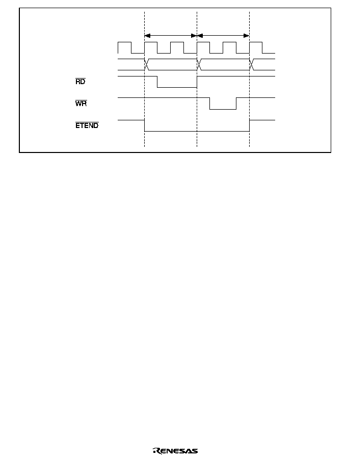
Rev. 2.0, 04/02, page 347 of 906
Address bus
¯
EXDMA
read cycle
EXDMA
write cycle
EDSAR
EDDAR
Figure 8.2 Example of Timing in Dual Address Mode
Single Address Mode: In single address mode, the
('$&. signal is used instead of the source or
destination address register to transfer data directly between an external device and external
memory. In this mode, the EXDMAC accesses the transfer source or transfer destination external
device by outputting the external I/O strobe signal (
('$&.), and at the same time accesses the
other external device in the transfer by outputting an address. In this way, DMA transfer can be
executed in one bus cycle. In the example of transfer between external memory and an external
device with DACK shown in figure 8.3, data is output to the data bus by the external device and
written to external memory in the same bus cycle.
The transfer direction, that is whether the external device with DACK is the transfer source or
transfer destination, can be specified with the SDIR bit in EDMDR. Transfer is performed from
the external memory (EDSAR) to the external device with DACK when SDIR = 0, and from the
external device with DACK to the external memory (EDDAR) when SDIR = 1.
The setting in the source or destination address register not used in the transfer is ignored.
The
('$&. pin becomes valid automatically when single address mode is selected. The ('$&.
pin is active-low.
(7(1' pin output can be enabled or disabled by means of the ETENDE bit in
EDMDR.
(7(1' is output for one bus cycle.
Figure 8.3 shows the data flow in single address mode, and figure 8.4 shows an example of the
timing.
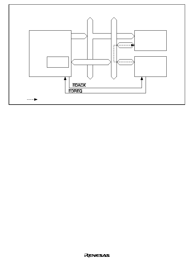
Rev. 2.0, 04/02, page 348 of 906
Microcomputer
Data flow
External
address bus
External
data bus
EXDMAC
External
memory
External device
with DACK
Figure 8.3 Data Flow in Single Address Mode
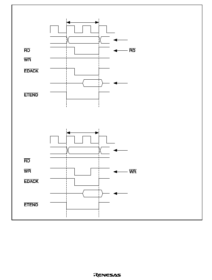
Rev. 2.0, 04/02, page 349 of 906
EXDMA cycle
EDSAR
Address to external memory space
signal to external memory space
Data output from external memory
Address bus
¯
¯
Data bus
EXDMA cycle
EDDAR
Address to external memory space
signal to external memory space
Address bus
Transfer from external memory to external device with DACK
Transfer from external device with DACK to external memory
Data bus
Data output from external device
with DACK
Figure 8.4 Example of Timing in Single Address Mode

Rev. 2.0, 04/02, page 350 of 906
8.4.3
DMA Transfer Requests
Auto Request Mode: In auto request mode, transfer request signals are automatically generated
within the EXDMAC in cases where a transfer request signal is not issued from outside, such as in
transfer between two memories, or between a peripheral module that is not capable of generating
transfer requests and memory. In auto request mode, transfer is started when the EDA bit is set to
1 in EDMDR.
In auto request mode, either cycle steal mode or burst mode can be selected as the bus mode.
Block transfer mode cannot be used.
External Request Mode: In external request mode, transfer is started by a transfer request signal
(
('5(4) from a device external to this LSI. DMA transfer is started when ('5(4 is input while
DMA transfer is enabled (EDA = 1).
The transfer request source need not be the data transfer source or data transfer destination.
The transfer request signal is accepted via the
('5(4 pin. Either falling edge sensing or low level
sensing can be selected for the
('5(4 pin by means of the EDREQS bit in EDMDR (low level
sensing when EDREQS = 0, falling edge sensing when EDREQS = 1).
Setting the EDRAKE bit to 1 in EDMDR enables a signal confirming transfer request acceptance
to be output from the
('5$K pin. The ('5$. signal is output when acceptance and transfer
processing has been started in response to a single external request. The
('5$. signal enables
the external device to determine the timing of
('5(4 signal negation, and makes it possible to
provide handshaking between the transfer request source and the EXDMAC.
In external request mode, block transfer mode can be used instead of burst mode. Block transfer
mode allows continuous execution (burst operation) of the specified number of transfers (the block
size) in response to a single transfer request. In block transfer mode, the
('5$. signal is output
only once for a one-block transfer, since the transfer request via the
('5(4 pin is for a block
unit.
8.4.4
Bus Modes
There are two bus modes: cycle steal mode and burst mode. When the activation source is an auto
request, either cycle steal mode or burst mode can be selected. When the activation source is an
external request, cycle steal mode is used.
Cycle Steal Mode: In cycle steal mode, the EXDMAC releases the bus at the end of each transfer
of a transfer unit (byte, word, or block). If there is a subsequent transfer request, the EXDMAC
takes back the bus, performs another transfer-unit transfer, and then releases the bus again. This
procedure is repeated until the transfer end condition is satisfied.

Rev. 2.0, 04/02, page 351 of 906
If a transfer request occurs in another channel during DMA transfer, the bus is temporarily
released, then transfer is performed on the channel for which the transfer request was issued. If
there is no external space bus request from another bus master, a one-cycle bus release interval is
inserted. For details on the operation when there are requests for a number of channels, see section
8.4.8, Channel Priority Order.
Figure 8.5 shows an example of the timing in cycle steal mode.
CPU
CPU
CPU
CPU
EXDMAC
EXDMAC
Bus returned temporarily to CPU
Bus cycle
Transfer conditions:
∑ Single address mode, normal transfer mode
∑
low level sensing
∑ CPU internal bus master is operating in external space
Figure 8.5 Example of Timing in Cycle Steal Mode
Burst Mode: In burst mode, once the EXDMAC acquires the bus it continues transferring data,
without releasing the bus, until the transfer end condition is satisfied. There is no burst mode in
external request mode.
In burst mode, once transfer is started it is not interrupted even if there is a transfer request from
another channel with higher priority. When the burst mode channel finishes its transfer, it releases
the bus in the next cycle in the same way as in cycle steal mode.
When the EDA bit is cleared to 0 in EDMDR, DMA transfer is halted. However, DMA transfer is
executed for all transfer requests generated within the EXDMAC up until the EDA bit was cleared
to 0.
If a repeat area overflow interrupt is generated, the EDA bit is cleared to 0 and transfer is
terminated.
When the BGUP bit is set to 1 in EDMDR, the bus is released if a bus request is issued by another
bus mastership during burst transfer. If there is no bus request, burst transfer is executed even if
the BGUP bit is set to 1.
Figure 8.6 shows examples of the timing in burst mode.
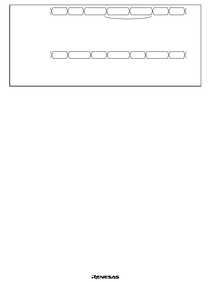
Rev. 2.0, 04/02, page 352 of 906
CPU
CPU
CPU
CPU
Bus cycle
EXDMAC operates alternately with CPU
EXDMAC
EXDMAC
EXDMAC
Transfer conditions:
Auto request mode, BGUP = 1
CPU
CPU
CPU
CPU
Bus cycle
CPU cycle not generated
EXDMAC
EXDMAC
EXDMAC
Transfer conditions:
Auto request mode, BGUP = 0
Figure 8.6 Examples of Timing in Burst Mode
8.4.5
Transfer Modes
There are two transfer modes: normal transfer mode and block transfer mode. When the activation
source is an external request, either normal transfer mode or block transfer mode can be selected.
When the activation source is an auto request, normal transfer mode is used.
Normal Transfer Mode: In normal transfer mode, transfer of one transfer unit is processed in
response to one transfer request. EDTCR functions as a 24-bit transfer counter.
The
(7(1' signal is output only for the last DMA transfer. The ('5$. signal is output each
time a transfer request is accepted and transfer processing is started.
Figure 8.7 shows examples of DMA transfer timing in normal transfer mode.

Rev. 2.0, 04/02, page 353 of 906
Read
Write
Read
Write
EXDMA
transfer cycle
Last EXDMA
transfer cycle
Bus cycle
Transfer conditions:
Dual address mode, auto request mode
EXDMA
EXDMA
Bus cycle
Transfer conditions:
Single address mode, external request mode
Figure 8.7 Examples of Timing in Normal Transfer Mode
Block Transfer Mode: In block transfer mode, the number of bytes or words specified by the
block size is transferred in response to one transfer request. The upper 8 bits of EDTCR specify
the block size, and the lower 16 bits function as a 16-bit transfer counter. A block size of 1 to 256
can be specified. During transfer of a block, transfer requests for other higher-priority channels are
held pending. When transfer of one block is completed, the bus is released in the next cycle.
When the BGUP bit is set to 1 in EDMDR, the bus is released if a bus request is issued by another
bus mastership during block transfer.
Address register values are updated in the same way as in normal mode. There is no function for
restoring the initial address register values after each block transfer.
The
(7(1' signal is output for each block transfer in the DMA transfer cycle in which the block
ends. The
('5$. signal is output once for one transfer request (for transfer of one block).
Caution is required when setting the repeat area overflow interrupt of the repeat area function in
block transfer mode. See section 8.4.6, Repeat Area Function, for details.
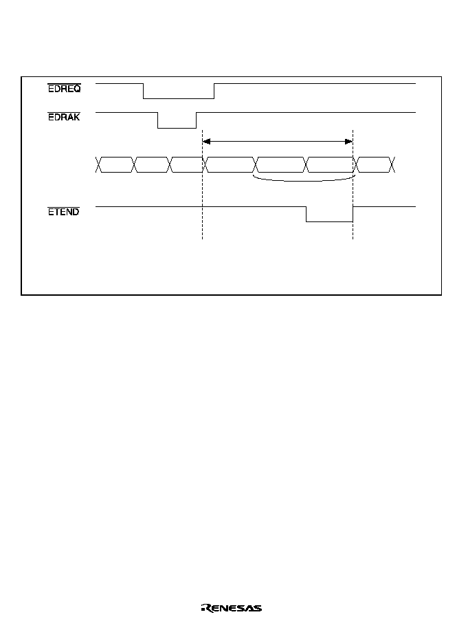
Rev. 2.0, 04/02, page 354 of 906
Block transfer is aborted if an NMI interrupt is generated. See section 8.4.12, Ending DMA
Transfer, for details.
Figure 8.8 shows an example of DMA transfer timing in block transfer mode.
CPU
CPU
CPU
EXDMAC
EXDMAC
EXDMAC
CPU
Bus cycle
CPU cycle not generated
One-block transfer cycle
Transfer conditions:
∑ Single address mode
∑ BGUP = 0
∑ Block size (EDTCR[23:16]) = 3
Figure 8.8 Example of Timing in Block Transfer Mode
8.4.6
Repeat Area Function
The EXDMAC has a function for designating a repeat area for source addresses and/or destination
addresses. When a repeat area is designated, the address register values repeat within the range
specified as the repeat area. Normally, when a ring buffer is involved in a transfer, an operation is
required to restore the address register value to the buffer start address each time the address
register value is the last address in the buffer (i.e. when ring buffer address overflow occurs), but if
the repeat area function is used, the operation that restores the address register value to the buffer
start address is performed automatically within the EXDMAC.
The repeat area function can be set independently for the source address register and the
destination address register.
The source address repeat area is specified by bits SARA4 to SARA0 in EDACR, and the
destination address repeat area by bits DARA4 to DARA0 in EDACR. The size of each repeat
area can be specified independently.
When the address register value is the last address in the repeat area and repeat area overflow
occurs, DMA transfer can be temporarily halted and an interrupt request sent to the CPU. If the
SARIE bit in EDACR is set to 1, when the source address register overflows the repeat area, the
Rev. 2.0, 04/02, page 355 of 906
IRF bit is set to 1 and the EDA bit cleared to 0 in EDMDR, and transfer is terminated. If EDIE = 1
in EDMDR, an interrupt is requested. If the DARIE bit in EDACR is set to 1, the above applies to
the destination address register.
If the EDA bit in EDMDR is set to 1 during interrupt generation, transfer is resumed. Figure 8.9
illustrates the operation of the repeat area function.
External memory
Repeated
Repeat area overflow
interrupt can be
requested
Range of
EDSAR values
H'23FFFE
H'23FFFF
H'240000
H'240001
H'240002
H'240003
H'240004
H'240005
H'240006
H'240007
H'240008
H'240009
H'240000
H'240001
H'240002
H'240003
H'240004
H'240005
H'240006
H'240007
:
:
When lower 3 bits (8-byte area) of EDSAR are designated as repeat area
(SARA4 to SARA0 = 3)
Figure 8.9 Example of Repeat Area Function Operation
Caution is required when the repeat area overflow interrupt function is used together with block
transfer mode. If transfer is always terminated when repeat area overflow occurs in block transfer
mode, the block size must be a power of two, or alternatively, the address register value must be
set so that the end of a block coincides with the end of the repeat area range.
If repeat area overflow occurs while a block is being transferred in block transfer mode, the repeat
interrupt request is held pending until the end of the block, and transfer overrun will occur. Figure
8.10 shows an example in which block transfer mode is used together with the repeat area
function.
Rev. 2.0, 04/02, page 356 of 906
External memory
Range of
EDSAR values
First block
transfer
Second block
transfer
H'23FFFE
H'23FFFF
H'240000
H'240001
H'240002
H'240003
H'240004
H'240005
H'240006
H'240007
H'240008
H'240009
H'240000
H'240001
H'240002
H'240003
H'240004
H'240005
H'240006
H'240007
H'240000
H'240001
H'240002
H'240003
H'240004
H'240000
H'240001
H'240005
H'240006
H'240007
:
:
Interrupt
requested
Block transfer
in progress
When lower 3 bits (8-byte area) of EDSAR are designated as repeat area (SARA4 to SARA0 = 3),
and block size of 5 (EDTCR[23≠16] = 5) is set in block transfer mode
Figure 8.10 Example of Repeat Area Function Operation in Block Transfer Mode
8.4.7
Registers during DMA Transfer Operation
EXDMAC register values are updated as DMA transfer processing is performed. The updated
values depend on various settings and the transfer status. The following registers and bits are
updated: EDSAR, EDDAR, EDTCR, and bits EDA, BEF, and IRF in EDMDR,
EXDMA Source Address Register (EDSAR): When the EDSAR address is accessed as the
transfer source, after the EDSAR value is output, EDSAR is updated with the address to be
accessed next. Bits SAT1 and SAT0 in EDACR specify incrementing or decrementing. The
address is fixed when SAT1 = 0, incremented when SAT1 = 1 and SAT0 = 0, and decremented
when SAT1 = 1 and SAT0 = 1.
The size of the increment or decrement is determined by the size of the data transferred. When the
DTSIZE bit in EDMDR = 0, the data is byte-size and the address is incremented or decremented
by 1; when DTSIZE = 1, the data is word-size and the address is incremented or decremented by
2.
When a repeat area setting is made, the operation conforms to that setting. The upper part of the
address set for the repeat area function is fixed, and is not affected by address updating.

Rev. 2.0, 04/02, page 357 of 906
When EDSAR is read during a transfer operation, a longword access must be used. During a
transfer operation, EDSAR may be updated without regard to accesses from the CPU, and the
correct values may not be read if the upper and lower words are read separately. In a longword
access, the EXDMAC buffers the EDSAR value to ensure that the correct value is output.
Do not write to EDSAR for a channel on which a transfer operation is in progress.
EXDMA Destination Address Register (EDDAR): When the EDDAR address is accessed as the
transfer destination, after the EDDAR value is output, EDDAR is updated with the address to be
accessed next. Bits DAT1 and DAT0 in EDACR specify incrementing or decrementing. The
address is fixed when DAT1 = 0, incremented when DAT1 = 1 and DAT0 = 0, and decremented
when DAT1 = 1 and DAT0 = 1.
The size of the increment or decrement is determined by the size of the data transferred. When the
DTSIZE bit in EDMDR = 0, the data is byte-size and the address is incremented or decremented
by 1; when DTSIZE = 1, the data is word-size and the address is incremented or decremented by
2.
When a repeat area setting is made, the operation conforms to that setting. The upper part of the
address set for the repeat area function is fixed, and is not affected by address updating.
When EDDAR is read during a transfer operation, a longword access must be used. During a
transfer operation, EDDAR may be updated without regard to accesses from the CPU, and the
correct values may not be read if the upper and lower words are read separately. In a longword
access, the EXDMAC buffers the EDDAR value to ensure that the correct value is output.
Do not write to EDDAR for a channel on which a transfer operation is in progress.
EXDMA Transfer Count Register (EDTCR): When a DMA transfer is performed, the value in
EDTCR is decremented by 1. However, when the EDTCR value is 0, transfers are not counted and
the EDTCR value does not change.
EDTCR functions differently in block transfer mode. The upper 8 bits, EDTCR[23:16], are used to
specify the block size, and their value does not change. The lower 16 bits, EDTCR[15:0], function
as a transfer counter, the value of which is decremented by 1 when a DMA transfer is performed.
However, when the EDTCR[15:0] value is 0, transfers are not counted and the EDTCR[15:0]
value does not change.
In normal transfer mode, all of the lower 24 bits of EDTCR may change, so when EDTCR is read
by the CPU during DMA transfer, a longword access must be used. During a transfer operation,
EDTCR may be updated without regard to accesses from the CPU, and the correct values may not
be read if the upper and lower words are read separately. In a longword access, the EXDMAC
buffers the EDTCR value to ensure that the correct value is output.
Rev. 2.0, 04/02, page 358 of 906
In block transfer mode, the upper 8 bits are never updated, so there is no problem with using word
access.
Do not write to EDTCR for a channel on which a transfer operation is in progress. If there is
contention between an address update associated with DMA transfer and a write by the CPU, the
CPU write has priority.
In the event of contention between an EDTCR update from 1 to 0 and a write (of a nonzero value)
by the CPU, the CPU write value has priority as the EDTCR value, but transfer is terminated.
Transfer does not end if the CPU writes 0 to EDTCR.
Figure 8.11 shows EDTCR update operations in normal transfer mode and block transfer mode.
23
0
0
EDTCR
Fixed
23
0
0
Before update
After update
23
0
1 to H'FFFFFF
EDTCR
≠1
23
0
0 to H'FFFFFE
EDTCR
EDTCR in normal transfer mode
EDTCR in block transfer mode
Fixed
Before update
After update
23
15
0
16
1 to H'FFFF
Block
size
EDTCR
≠1
23
15
0
16
0
Block
size
23
15
0
16
0 to H'FFFE
Block
size
23
15
0
16
0
Block
size
Figure 8.11 EDTCR Update Operations in Normal Transfer Mode and
Block Transfer Mode
EDA Bit in EDMDR: The EDA bit in EDMDR is written to by the CPU to control enabling and
disabling of data transfer, but may be cleared automatically by the EXDMAC due to the DMA
transfer status. There are also periods during transfer when a 0-write to the EDA bit by the CPU is
not immediately effective.
Conditions for EDA bit clearing by the EXDMAC include the following:
∑
When the EDTCR value changes from 1 to 0, and transfer ends
∑
When a repeat area overflow interrupt is requested, and transfer ends
Rev. 2.0, 04/02, page 359 of 906
∑
When an NMI interrupt is generated, and transfer halts
∑
A reset
∑
Hardware standby mode
∑
When 0 is written to the EDA bit, and transfer halts
When transfer is halted by writing 0 to the EDA bit, the EDA bit remains at 1 during the DMA
transfer period. In block transfer mode, since a block-size transfer is carried out without
interruption, the EDA bit remains at 1 from the time 0 is written to it until the end of the current
block-size transfer.
In burst mode, transfer is halted for up to three DMA transfers following the bus cycle in which 0
is written to the EDA bit. The EDA bit remains set to 1 from the time of the 0-write until the end
of the last DMA cycle.
Writes (except to the EDA bit) are prohibited to registers of a channel for which the EDA bit is set
to 1. When changing register settings after a 0-write to the EDA bit, it is necessary to confirm that
the EDA bit has been cleared to 0.
Figure 8.12 shows the procedure for changing register settings in an operating channel.
Read EDA bit
Write 0 to EDA bit
Change register settings
EDA bit = 0?
1
2
3
4
1. Write 0 to the EDA bit in EDMDR.
2. Read the EDA bit.
3. Confirm that EDA = 0. If EDA = 1, this
indicates that DMA transfer is in progress.
4. Write the required set values to the
registers.
No
Yes
Changing register settings
in operating channel
Register setting
changes completed
Figure 8.12 Procedure for Changing Register Settings in Operating Channel
BEF Bit in EDMDR: In block transfer mode, the specified number of transfers (equivalent to the
block size) is performed in response to a single transfer request. To ensure that the correct number

Rev. 2.0, 04/02, page 360 of 906
of transfers is carried out, a block-size transfer is always executed, except in the event of a reset,
transition to standby mode, or generation of an NMI interrupt.
If an NMI interrupt is generated during block transfer, operation is halted midway through a
block-size transfer and the EDA bit is cleared to 0, terminating the transfer operation. In this case
the BEF bit, which indicates the occurrence of an error during block transfer, is set to 1.
IRF Bit in EDMDR: The IRF bit in EDMDR is set to 1 when an interrupt request source occurs.
If the EDIE bit in EDMDR is 1 at this time, an interrupt is requested.
The timing for setting the IRF bit to 1 is when the EDA bit in EDMDR is cleared to 0 and transfer
ends following the end of the DMA transfer bus cycle in which the source generating the interrupt
occurred.
If the EDA bit is set to 1 and transfer is resumed during interrupt handling, the IRF bit is
automatically cleared to 0 and the interrupt request is cleared.
For details on interrupts, see section 8.5, Interrupts Sources.
8.4.8
Channel Priority Order
The priority order of the EXDMAC channels is: channel 0 > channel 1 > channel 2 > channel 3.
Table 8.3 shows the EXDMAC channel priority order.
Table 8.3
EXDMAC Channel Priority Order
Channel
Priority
Channel 0
High
Channel 1
Channel 2
Channel 3
Low
If transfer requests occur simultaneously for a number of channels, the highest-priority channel
according to the priority order in table 8.3 is selected for transfer.
Transfer Requests from Multiple Channels (Except Auto Request Cycle Steal Mode): If
transfer requests for different channels are issued during a transfer operation, the highest-priority
channel (excluding the currently transferring channel) is selected. The selected channel begins
transfer after the currently transferring channel releases the bus. If there is a bus request from a bus
mastership other than the EXDMAC at this time, a cycle for the other bus mastership is initiated.
If there is no other bus request, the bus is released for one cycle.
Channels are not switched during burst transfer or transfer of a block in block transfer mode.
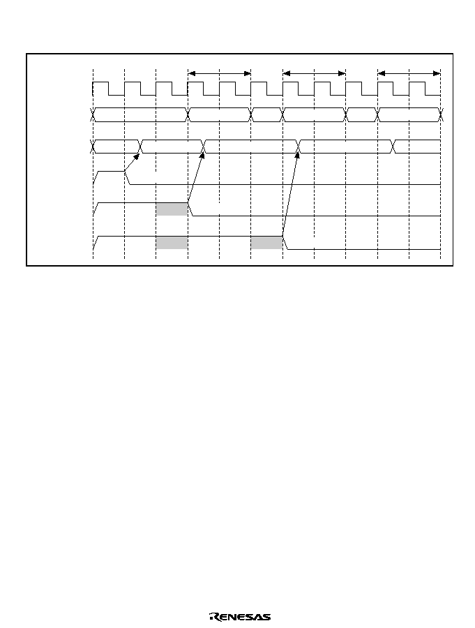
Rev. 2.0, 04/02, page 361 of 906
Figure 8.13 shows an example of the transfer timing when transfer requests occur simultaneously
for channels 0, 1, and 2. The example in the figure is for external request cycle steal mode.
Channel 0 transfer
Idle
Bus
release
Address bus
EXDMA control
Channel 0
Channel 1
Channel 1 transfer
Channel 2 transfer
Channel 2
Channel 0
Channel 1
Channel 2
Channel 0
Request
held
Selected
Request
held
Request
held
Not
selected
Selected
Channel 1
Request cleared
Request cleared
Request cleared
Bus
release
Channel 2
¯
Figure 8.13 Example of Channel Priority Timing
Transfer Requests from Multiple Channels in Auto Request Cycle Steal Mode: If transfer
requests for different channels are issued during a transfer in auto request cycle steal mode, the
operation depends on the channel priority. If the channel that made the transfer request is of higher
priority than the channel currently performing transfer, the channel that made the transfer request
is selected.
If the channel that made the transfer request is of lower priority than the channel currently
performing transfer, that channel's transfer request is held pending, and the currently transferring
channel remains selected.
The selected channel begins transfer after the currently transferring channel releases the bus. If
there is a bus request from a bus mastership other than the EXDMAC at this time, a cycle for the
other bus mastership is initiated. If there is no other bus request, the bus is released for one cycle.
Figure 8.14 shows examples of transfer timing in cases that include auto request cycle steal mode.
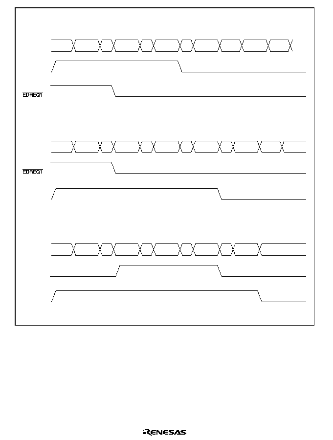
Rev. 2.0, 04/02, page 362 of 906
Channel 0
Channel 0
Channel 0
Channel 1
Channel 1
Bus
Conditions (1)
Channel 0: Auto request, cycle steal mode
Channel 1: External request, cycle steal mode, low level activation
Channel 0
EDA bit
Channel 1/
pin
Channel 2
Channel 2
Channel 1
Channel 1
Channel 2
Channel 1
Bus
Conditions (2)
Channel 1: External request, cycle steal mode, low level activation
Channel 2: Auto request, cycle steal mode
Channel 1/
pin
Channel 2
EDA bit
Channel 2
Channel 2
Channel 0
Channel 2
Channel 0
Bus
Conditions (3)
Channel 0: Auto request, cycle steal mode
Channel 2: Auto request, cycle steal mode
*
: Bus release
Channel 0
EDA bit
Channel 2
EDA bit
*
*
*
*
*
*
*
*
*
*
*
*
*
*
*
Figure 8.14 Examples of Channel Priority Timing
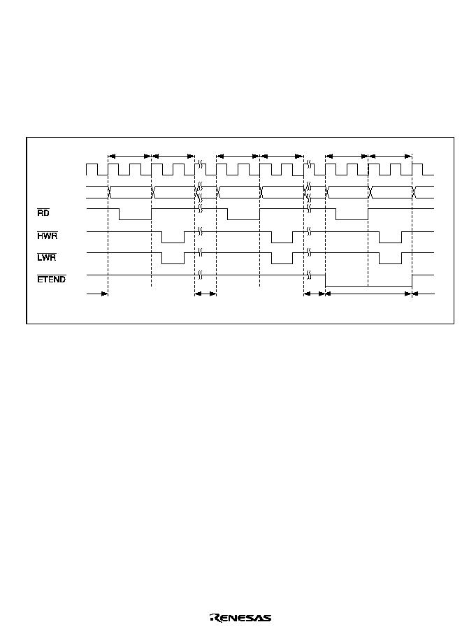
Rev. 2.0, 04/02, page 363 of 906
8.4.9
EXDMAC Bus Cycles (Dual Address Mode)
Normal Transfer Mode (Cycle Steal Mode): Figure 8.15 shows an example of transfer when
(7(1' output is enabled, and word-size, normal transfer mode (cycle steal mode) is performed
from external 16-bit, 2-state access space to external 16-bit, 2-state access space.
After one byte or word has been transferred, the bus is released. While the bus is released, one
CPU, DMAC, or DTC bus cycle is initiated.
DMA read DMA write
DMA read DMA write
DMA read DMA write
Address bus
Bus
release
Bus
release
Bus
release
Bus
release
Last transfer
cycle
¯
Figure 8.15 Example of Normal Transfer Mode (Cycle Steal Mode) Transfer
Normal Transfer Mode (Burst Mode): Figure 8.16 shows an example of transfer when
(7(1'
output is enabled, and word-size, normal transfer mode (burst mode) is performed from external
16-bit, 2-state access space to external 16-bit, 2-state access space.
In burst mode, one-byte or one-word transfers are executed continuously until transfer ends.
Once burst transfer starts, requests from other channels, even of higher priority, are held pending
until transfer ends.
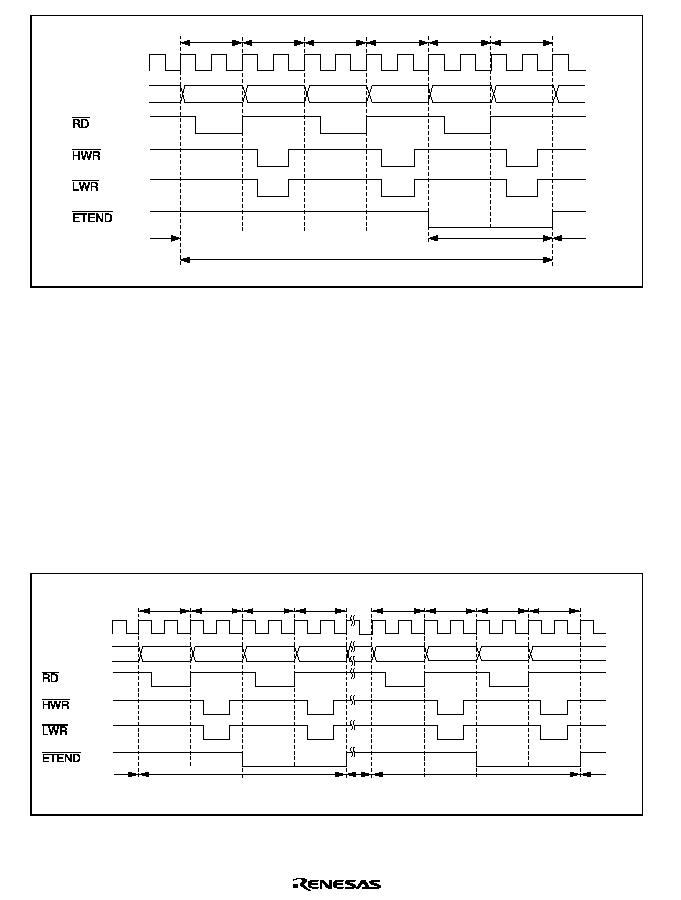
Rev. 2.0, 04/02, page 364 of 906
DMA read DMA write DMA read DMA write DMA read DMA write
Address bus
Bus
release
Bus
release
Last transfer cycle
Burst transfer
¯
Figure 8.16 Example of Normal Transfer Mode (Burst Mode) Transfer
If an NMI interrupt is generated while a channel designated for burst transfer is enabled for
transfer, the EDA bit is cleared and transfer is disabled. If a block transfer has already been
initiated within the EXDMAC, the bus is released on completion of the currently executing byte or
word transfer, and burst transfer is aborted. If the last transfer cycle in burst transfer has been
initiated within the EXDMAC, transfer is executed to the end even if the EDA bit is cleared.
Block Transfer Mode (Cycle Steal Mode): Figure 8.17 shows an example of transfer when
(7(1' output is enabled, and word-size, block transfer mode (cycle steal mode) is performed
from external 16-bit, 2-state access space to external 16-bit, 2-state access space.
One block is transferred in response to one transfer request, and after the transfer, the bus is
released. While the bus is released, one or more CPU, DMAC, or DTC bus cycles are initiated.
DMA
read
DMA
write
Address bus
Bus
release
Bus
release
Bus
release
Last block transfer
DMA
read
Block transfer
DMA
write
DMA
read
DMA
write
DMA
read
DMA
write
¯
Figure 8.17 Example of Block Transfer Mode (Cycle Steal Mode) Transfer
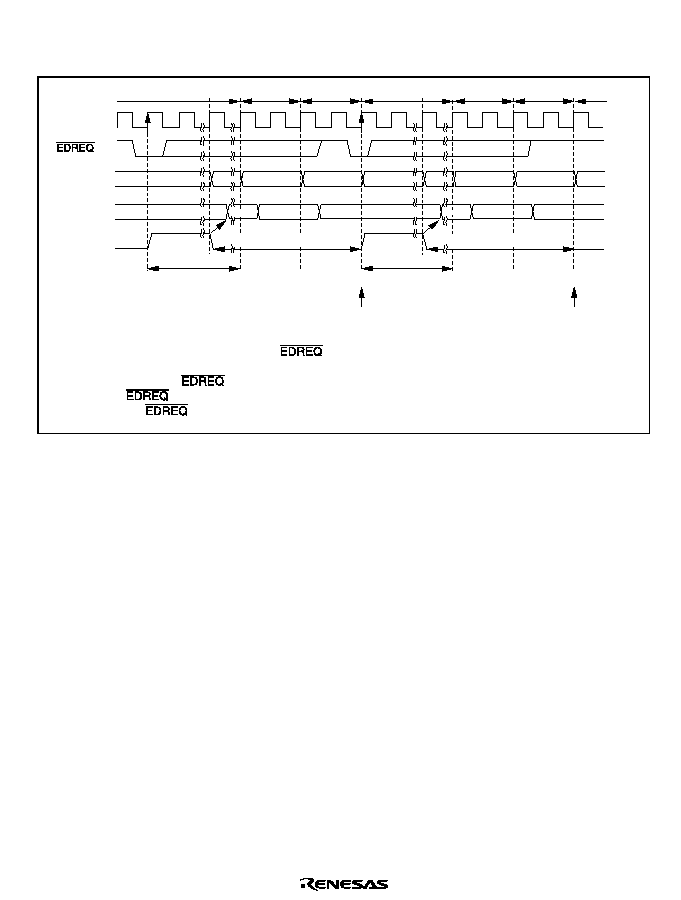
Rev. 2.0, 04/02, page 365 of 906
#"
#" Pin Falling Edge Activation Timing: Figure 8.18 shows an example of normal mode
transfer activated by the
('5(4 pin falling edge.
DMA read
DMA write
¯
Address bus
Write
Idle
Bus release
Transfer
destination
DMA control
Channel
Write
Idle
Transfer source
Transfer source
Bus release
DMA read
DMA write Bus release
Request
Request
[1]
[3]
[2]
[4]
[5]
[6]
[7]
Acceptance
resumed
Acceptance
resumed
Read
Read
Idle
[1]
Acceptance after transfer enabling;
pin low level is sampled at rise of ¯, and request is held.
[2], [5] Request is cleared at end of next bus cycle, and activation is started in EXDMAC.
[3], [6] DMA cycle start;
pin high level sampling is started at rise of ¯.
[4], [7] When
pin high level has been sampled, acceptance is resumed after completion of write cycle.
(As in [1],
pin low level is sampled at rise of ¯, and request is held.)
Transfer
destination
Request clearance period
Request clearance period
Minimum 3 cycles
Minimum 3 cycles
Figure 8.18 Example of Normal Mode Transfer Activated by
#"
#" Pin Falling Edge
('5(4 pin sampling is performed in each cycle starting at the next rise of ¯ after the end of the
EDMDR write cycle for setting the transfer-enabled state.
When a low level is sampled at the
('5(4 pin while acceptance via the ('5(4 pin is possible,
the request is held within the EXDMAC. Then when activation is initiated within the EXDMAC,
the request is cleared, and
('5(4 pin high level sampling for edge sensing is started. If ('5(4
pin high level sampling is completed by the end of the DMA write cycle, acceptance resumes after
the end of the write cycle, and
('5(4 pin low level sampling is performed again; this sequence
of operations is repeated until the end of the transfer.
Figure 8.19 shows an example of block transfer mode transfer activated by the
('5(4 pin falling
edge.
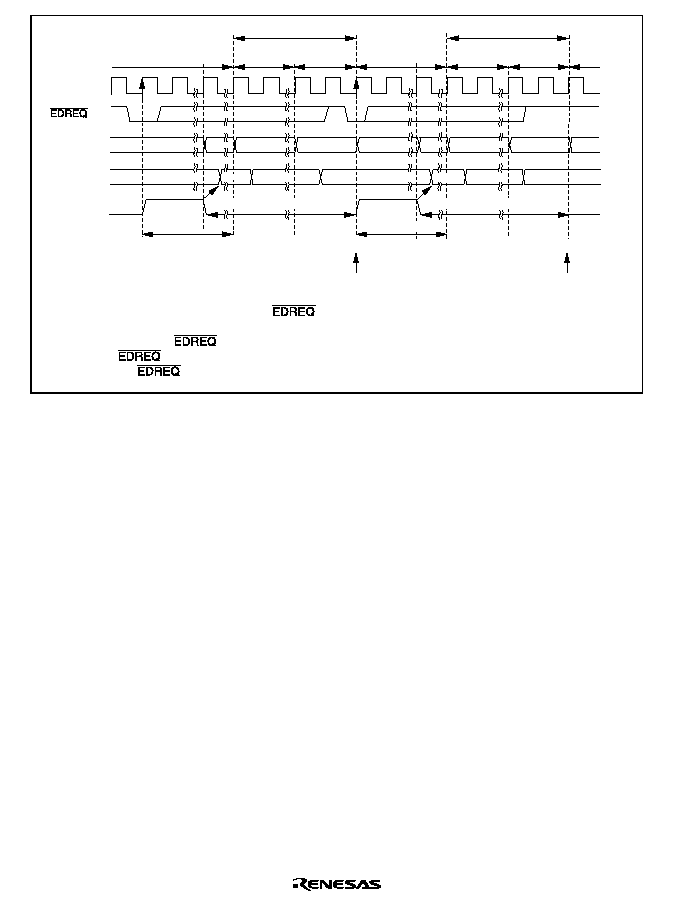
Rev. 2.0, 04/02, page 366 of 906
DMA read
DMA write
¯
Address bus
Idle
Write
Bus release
Transfer
destination
DMA control
Channel
Write
Idle
Transfer source
Transfer
destination
Transfer source
Request
Request
Minimum 3 cycles
Acceptance
resumed
Acceptance
resumed
Read
Bus release
DMA read
DMA write
Bus release
One block transfer
One block transfer
Idle
[1]
[4]
[5]
[6]
[7]
[3]
[2]
[1]
Acceptance after transfer enabling;
pin low level is sampled at rise of ¯, and request is held.
[2], [5] Request is cleared at end of next bus cycle, and activation is started in EXDMAC.
[3], [6] DMA cycle start;
pin high level sampling is started at rise of ¯.
[4], [7] When
pin high level has been sampled, acceptance is resumed after completion of dead cycle.
(As in [1],
pin low level is sampled at rise of ¯, and request is held.)
Read
Request clearance period
Request clearance period
Minimum 3 cycles
Figure 8.19 Example of Block Transfer Mode Transfer Activated by
#"
#" Pin Falling
Edge
('5(4 pin sampling is performed in each cycle starting at the next rise of ¯ after the end of the
EDMDR write cycle for setting the transfer-enabled state.
When a low level is sampled at the
('5(4 pin while acceptance via the ('5(4 pin is possible,
the request is held within the EXDMAC. Then when activation is initiated within the EXDMAC,
the request is cleared, and
('5(4 pin high level sampling for edge sensing is started. If ('5(4
pin high level sampling is completed by the end of the DMA write cycle, acceptance resumes after
the end of the write cycle, and
('5(4 pin low level sampling is performed again; this sequence
of operations is repeated until the end of the transfer.
#"
#" Pin Low Level Activation Timing: Figure 8.20 shows an example of normal mode
transfer activated by the
('5(4 pin low level.
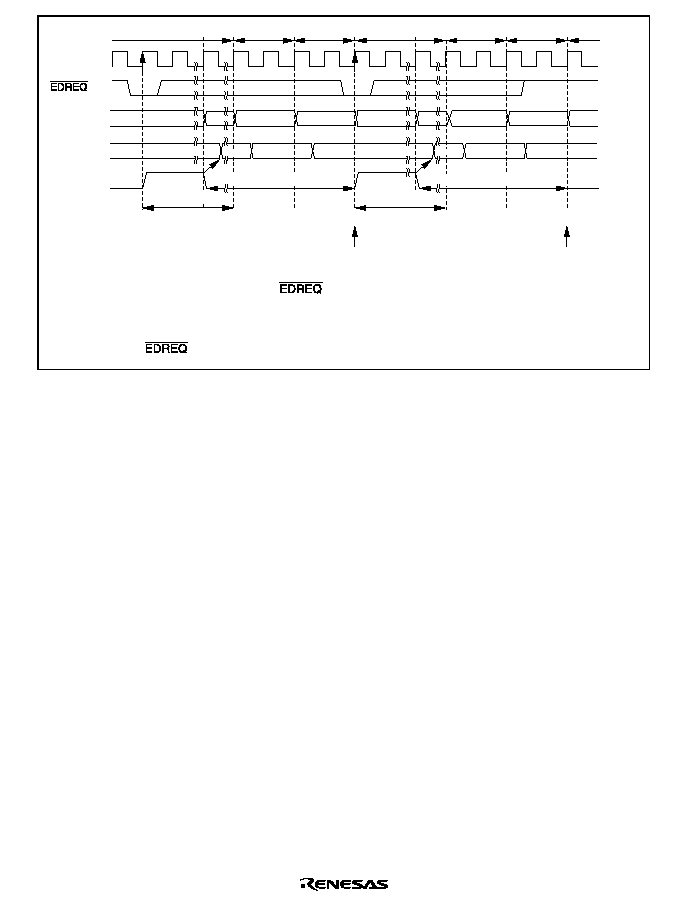
Rev. 2.0, 04/02, page 367 of 906
DMA read
DMA write
¯
Address bus
Idle
Write
Idle
Bus release
DMA control
Channel
Write
Idle
Transfer source
Bus release
DMA read
DMA write
Request
Read
Read
Transfer
destination
Transfer source
Transfer
destination
Bus release
[1]
[3]
[2]
[4]
[6]
[5]
[7]
Acceptance
resumed
Acceptance
resumed
[1]
Acceptance after transfer enabling;
pin low level is sampled at rise of ¯, and request is held.
[2], [5] Request is cleared at end of next bus cycle, and activation is started in EXDMAC.
[3], [6] DMA cycle is started.
[4], [7] Acceptance is resumed after completion of write cycle.
(As in [1],
pin low level is sampled at rise of ¯, and request is held.)
Minimum 3 cycles
Request
Minimum 3 cycles
Request clearance period
Request clearance period
Figure 8.20 Example of Normal Mode Transfer Activated by
#"
#" Pin Low Level
('5(4 pin sampling is performed in each cycle starting at the next rise of ¯ after the end of the
EDMDR write cycle for setting the transfer-enabled state.
When a low level is sampled at the
('5(4 pin while acceptance via the ('5(4 pin is possible,
the request is held within the EXDMAC. Then when activation is initiated within the EXDMAC,
the request is cleared. At the end of the write cycle, acceptance resumes and
('5(4 pin low level
sampling is performed again; this sequence of operations is repeated until the end of the transfer.
Figure 8.21 shows an example of block transfer mode transfer activated by the
('5(4 pin low
level.
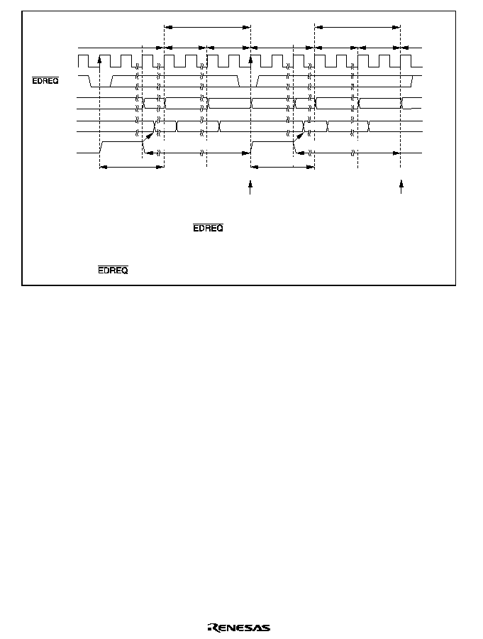
Rev. 2.0, 04/02, page 368 of 906
DMA read
DMA write
¯
Address bus
Idle
Write
Bus release
DMA control
Channel
Write
Idle
Read
Bus release
DMA read
DMA write
One block transfer
One block transfer
Idle
Transfer
destination
Transfer source
Transfer
destination
Transfer source
[1]
[3]
[2]
[4]
[6]
[5]
[7]
Acceptance
resumed
Acceptance
resumed
Bus release
[1]
Acceptance after transfer enabling;
pin low level is sampled at rise of ¯, and request is held.
[2], [5] Request is cleared at end of next bus cycle, and activation is started in EXDMAC.
[3], [6] DMA cycle is started.
[4], [7] Acceptance is resumed after completion of dead cycle.
(As in [1],
pin low level is sampled at rise of ¯, and request is held.)
Minimum 3 cycles
Request
Request
Read
Minimum 3 cycles
Request clearance period
Request clearance period
Figure 8.21 Example of Block Transfer Mode Transfer Activated by
#"
#" Pin Low Level
('5(4 pin sampling is performed in each cycle starting at the next rise of ¯ after the end of the
EDMDR write cycle for setting the transfer-enabled state.
When a low level is sampled at the
('5(4 pin while acceptance via the ('5(4 pin is possible,
the request is held within the EXDMAC. Then when activation is initiated within the EXDMAC,
the request is cleared. At the end of the write cycle, acceptance resumes and
('5(4 pin low level
sampling is performed again; this sequence of operations is repeated until the end of the transfer.
8.4.10
EXDMAC Bus Cycles (Single Address Mode)
Single Address Mode (Read): Figure 8.22 shows an example of transfer when
(7(1' output is
enabled, and byte-size, single address mode transfer (read) is performed from external 8-bit, 2-
state access space to an external device.
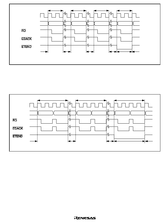
Rev. 2.0, 04/02, page 369 of 906
Address bus
Bus release
Bus release
Bus release
Last
transfer
cycle
DMA read
DMA read
DMA read
DMA read
Bus release
Bus release
¯
Figure 8.22 Example of Single Address Mode (Byte Read) Transfer
Figure 8.23 shows an example of transfer when
(7(1' output is enabled, and word-size, single
address mode transfer (read) is performed from external 8-bit, 2-state access space to an external
device.
DMA read
Address bus
Bus release
Bus release
Bus
release
Last transfer cycle
Bus release
DMA read
DMA read
¯
Figure 8.23 Example of Single Address Mode (Word Read) Transfer
After one byte or word has been transferred in response to one transfer request, the bus is released.
While the bus is released, one or more CPU, DMAC, or DTC bus cycles are initiated.
Single Address Mode (Write): Figure 8.24 shows an example of transfer when
(7(1' output is
enabled, and byte-size, single address mode transfer (write) is performed from an external device
to external 8-bit, 2-state access space.
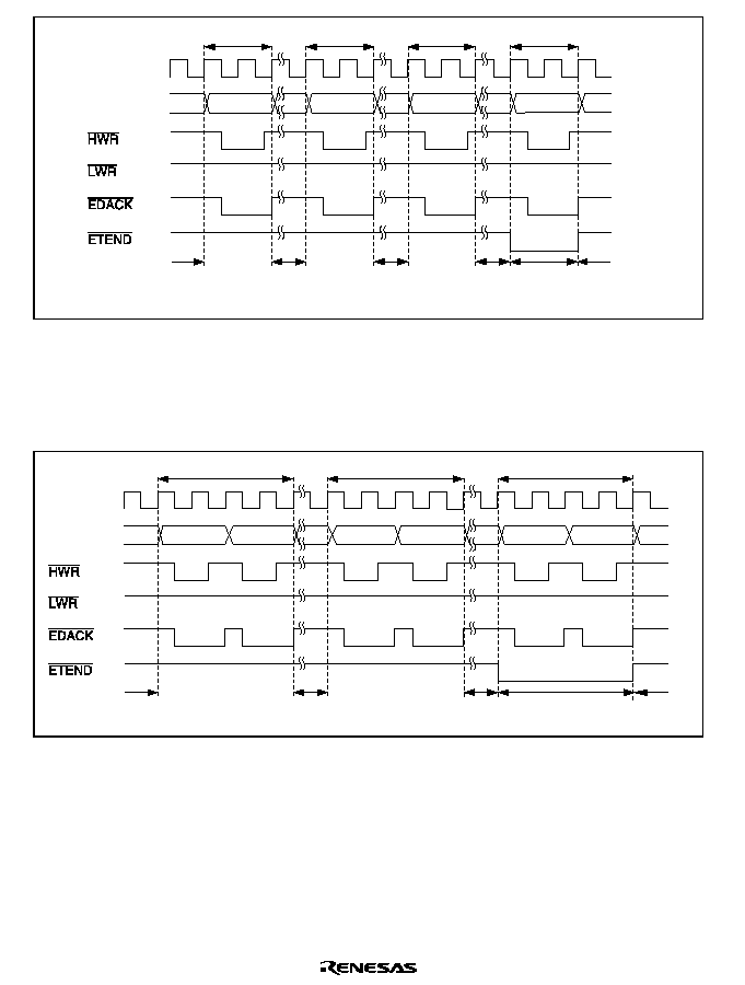
Rev. 2.0, 04/02, page 370 of 906
Address bus
Bus release
Bus release
Bus release
Last
transfer
cycle
DMA write
DMA write
DMA write
DMA write
Bus release
Bus release
¯
Figure 8.24 Example of Single Address Mode (Byte Write) Transfer
Figure 8.25 shows an example of transfer when
(7(1' output is enabled, and word-size, single
address mode transfer (write) is performed from an external device to external 8-bit, 2-state access
space.
DMA write
Address bus
Bus release
Bus release
Bus
release
Last transfer cycle
Bus release
DMA write
DMA write
¯
Figure 8.25 Example of Single Address Mode (Word Write) Transfer
After one byte or word has been transferred in response to one transfer request, the bus is released.
While the bus is released, one or more CPU, DMAC, or DTC bus cycles are initiated.
#"
#" Pin Falling Edge Activation Timing: Figure 8.26 shows an example of single address
mode transfer activated by the
('5(4 pin falling edge.
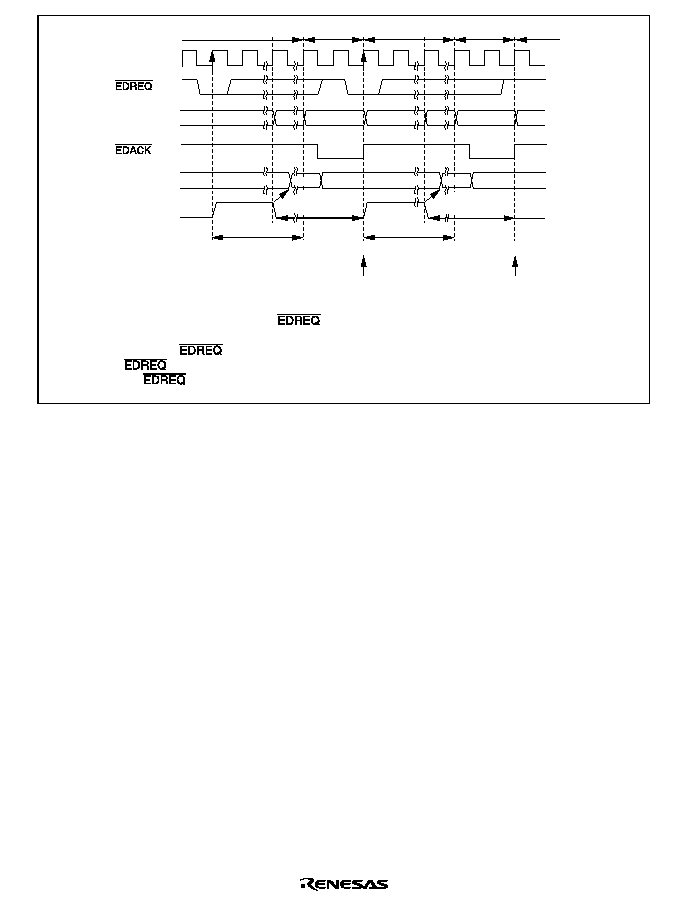
Rev. 2.0, 04/02, page 371 of 906
DMA single
¯
Address bus
Idle
Bus release
DMA control
Channel
Transfer source/
destination
Transfer source/
destination
Bus release
Idle
DMA single Bus release
Single
Single
Idle
[1]
[3]
[2]
[4]
[6]
[5]
[7]
Acceptance
resumed
Acceptance
resumed
[1]
Acceptance after transfer enabling;
pin low level is sampled at rise of ¯, and request is held.
[2], [5] Request is cleared at end of next bus cycle, and activation is started in EXDMAC.
[3], [6] DMA cycle start;
pin high level sampling is started at rise of ¯.
[4], [7] When
pin high level has been sampled, acceptance is resumed after completion of single cycle.
(As in [1],
pin low level is sampled at rise of ¯, and request is held.)
Request
clearance period
Request
clearance period
Minimum 3 cycles
Request
Minimum 3 cycles
Request
Figure 8.26 Example of Single Address Mode Transfer Activated by
##"
" Pin Falling
Edge
('5(4 pin sampling is performed in each cycle starting at the next rise of ¯ after the end of the
EDMDR write cycle for setting the transfer-enabled state.
When a low level is sampled at the
('5(4 pin while acceptance via the ('5(4 pin is possible,
the request is held within the EXDMAC. Then when activation is initiated within the EXDMAC,
the request is cleared, and
('5(4 pin high level sampling for edge sensing is started. If ('5(4
pin high level sampling is completed by the end of the DMA single cycle, acceptance resumes
after the end of the single cycle, and
('5(4 pin low level sampling is performed again; this
sequence of operations is repeated until the end of the transfer.
#"
#" Pin Low Level Activation Timing: Figure 8.27 shows an example of single address
mode transfer activated by the
('5(4 pin low level.
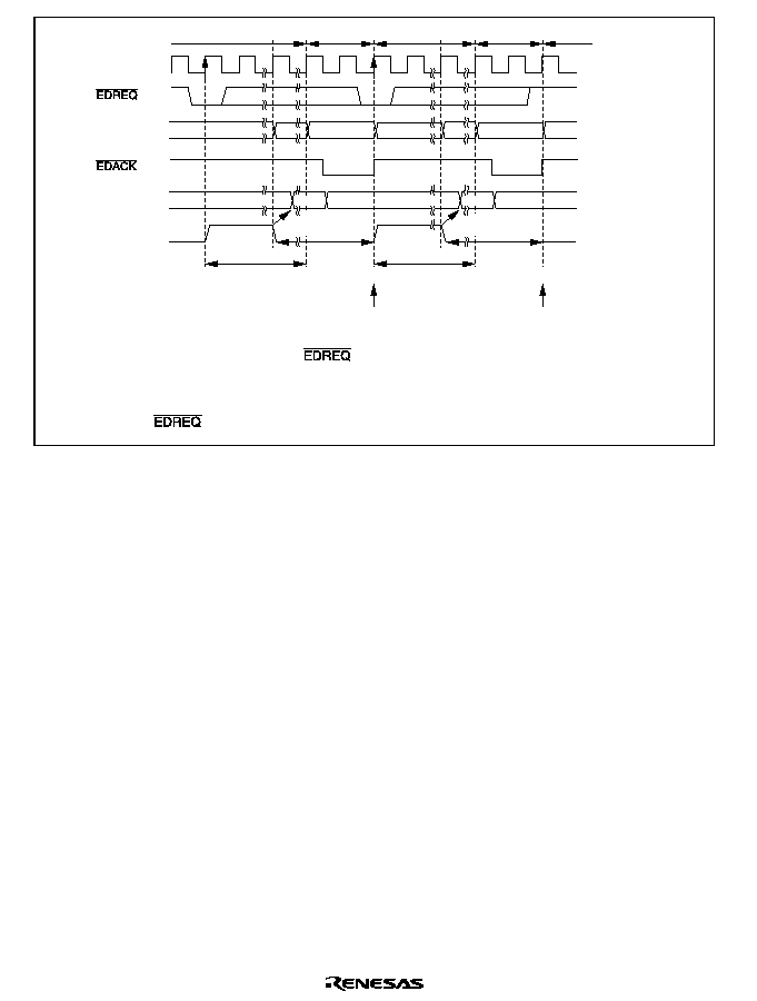
Rev. 2.0, 04/02, page 372 of 906
Single
Single
DMA single
¯
Address bus
Idle
Bus release
DMA control
Channel
Transfer source/
destination
Transfer source/
destination
Bus release
Idle
DMA single Bus release
Idle
[1]
[3]
[2]
[4]
[6]
[5]
[7]
Acceptance
resumed
Acceptance
resumed
Request
clearance period
Request
clearance period
Request
Request
Minimum 3 cycles
Minimum 3 cycles
[1]
Acceptance after transfer enabling;
pin low level is sampled at rise of ¯, and request is held.
[2], [5] Request is cleared at end of next bus cycle, and activation is started in EXDMAC.
[3], [6] DMA cycle is started.
[4], [7] Acceptance is resumed after completion of single cycle.
(As in [1],
pin low level is sampled at rise of ¯, and request is held.)
Figure 8.27 Example of Single Address Mode Transfer Activated by
##"
" Pin Low Level
('5(4 pin sampling is performed in each cycle starting at the next rise of ¯ after the end of the
EDMDR write cycle for setting the transfer-enabled state.
When a low level is sampled at the
('5(4 pin while acceptance via the ('5(4 pin is possible,
the request is held within the EXDMAC. Then when activation is initiated within the EXDMAC,
the request is cleared. At the end of the single cycle, acceptance resumes and
('5(4 pin low
level sampling is performed again; this sequence of operations is repeated until the end of the
transfer.

Rev. 2.0, 04/02, page 373 of 906
8.4.11
Examples of Operation Timing in Each Mode
Auto Request/Cycle Steal Mode/Normal Transfer Mode: When the EDA bit is set to 1 in
EDMDR, an EXDMA transfer cycle is started a minimum of three cycles later. There is a one-
cycle bus release interval between the end of a one-transfer-unit EXDMA cycle and the start of the
next transfer.
If there is a transfer request for another channel of higher priority, the transfer request by the
original channel is held pending, and transfer is performed on the higher-priority channel from the
next transfer. Transfer on the original channel is resumed on completion of the higher-priority
channel transfer.
Figures 8.28 to 8.30 show operation timing examples for various conditions.
¯ pin
Bus cycle
CPU
operation
EDA bit
EXDMA
read
EDA = 1
write
0
0
1
EXDMA
write
EXDMA
read
EXDMA
write
EXDMA
read
EXDMA
write
3 cycles
1 cycle
Last transfer cycle
Internal bus space
cycles
Bus release
Bus
release
Bus
release
Figure 8.28 Auto Request/Cycle Steal Mode/Normal Transfer Mode
(No Contention/Dual Address Mode)
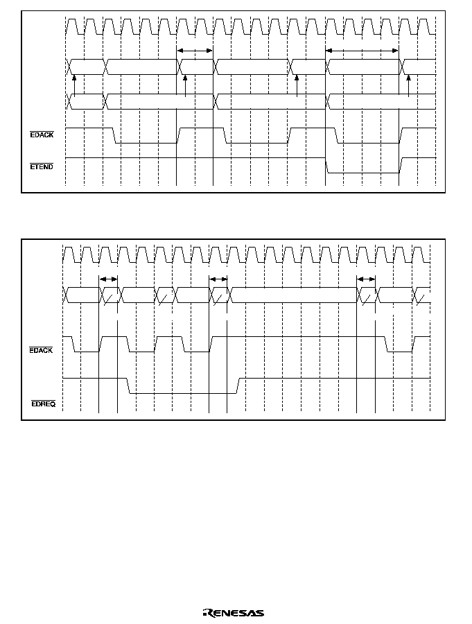
Rev. 2.0, 04/02, page 374 of 906
¯ pin
Bus cycle
CPU
operation
CPU cycle
EXDMA single
transfer cycle
External
space
CPU cycle
CPU cycle
CPU cycle
1 bus cycle
Last transfer cycle
EXDMA single
transfer cycle
EXDMA single
transfer cycle
External space
External space
External space
Figure 8.29 Auto Request/Cycle Steal Mode/Normal Transfer Mode
(CPU Cycles/Single Address Mode)
¯ pin
Bus cycle
Current
channel
Other
channel
transfer
request
(
)
EXDMA
single cycle
1 cycle
1 cycle
1 cycle
Higher-priority channel EXDMA cycle
EXDMA
single cycle
EXDMA
single cycle
EXDMA
single cycle
Bus
release
Bus
release
Bus
release
Bus
release
Bus
release
Figure 8.30 Auto Request/Cycle Steal Mode/Normal Transfer Mode
(Contention with Another Channel/Single Address Mode)
Auto Request/Burst Mode/Normal Transfer Mode: When the EDA bit is set to 1 in EDMDR,
an EXDMA transfer cycle is started a minimum of three cycles later. Once transfer is started, it
continues (as a burst) until the transfer end condition is satisfied.
If the BGUP bit is 1 in EDMDR, the bus is transferred in the event of a bus request from another
bus master.
Transfer requests for other channels are held pending until the end of transfer on the current
channel.
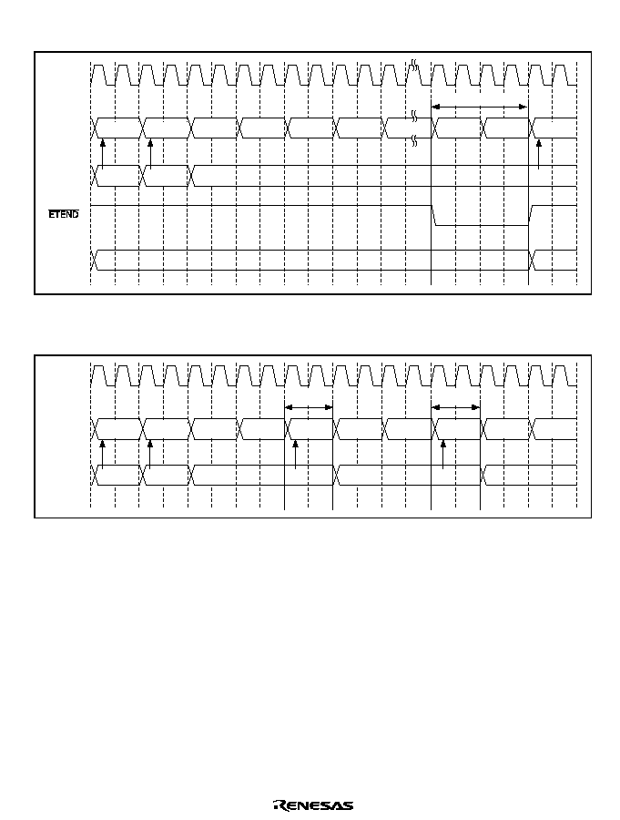
Rev. 2.0, 04/02, page 375 of 906
Figures 8.31 to 8.34 show operation timing examples for various conditions.
¯ pin
Bus cycle
CPU
operation
EDA bit
EXDMA
read
EXDMA
write
EXDMA
read
EXDMA
write
EXDMA
read
EXDMA
write
External
space
External
space
External
space
0
1
Repeated
Last transfer cycle
CPU cycle CPU cycle
CPU cycle
Figure 8.31 Auto Request/Burst Mode/Normal Transfer Mode
(CPU Cycles/Dual Address Mode/BGUP = 0)
¯ pin
Bus cycle
CPU
operation
EXDMA
read
EXDMA
write
EXDMA
read
EXDMA
write
EXDMA
read
EXDMA
write
External
space
External
space
External
space
External
space
1 bus cycle
1 bus cycle
CPU cycle CPU cycle
CPU cycle
CPU cycle
Figure 8.32 Auto Request/Burst Mode/Normal Transfer Mode
(CPU Cycles/Dual Address Mode/BGUP = 1)
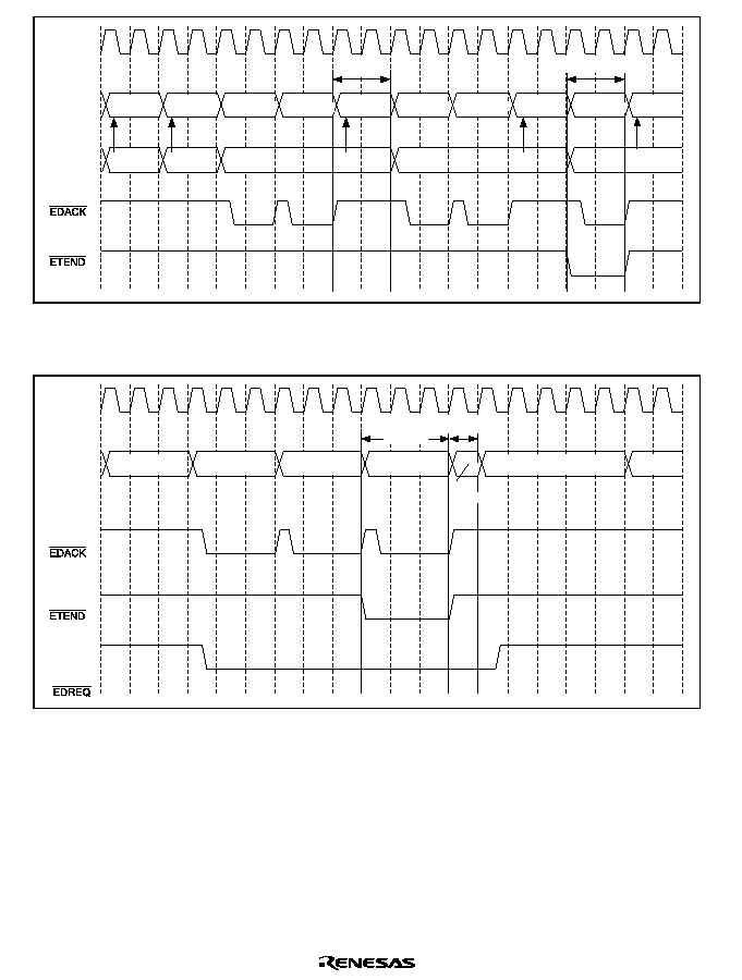
Rev. 2.0, 04/02, page 376 of 906
CPU cycle CPU cycle
CPU cycle
CPU cycle
CPU cycle
External
space
External
space
External
space
External
space
External
space
1 bus cycle
Last transfer cycle
¯ pin
Bus cycle
CPU
operation
EXDMA
single cycle
EXDMA
single cycle
EXDMA
single cycle
EXDMA
single cycle
EXDMA
single cycle
Figure 8.33 Auto Request/Burst Mode/Normal Transfer Mode
(CPU Cycles/Single Address Mode/BGUP = 1)
¯ pin
Bus cycle
Original
channel
Original
channel
Other
channel
transfer
request
(
)
EXDMA single
transfer cycle
EXDMA single
transfer cycle
EXDMA single
transfer cycle
1 cycle
Last transfer
cycle
Other channel EXDMA cycle
Bus release
Bus
release
Bus
release
Figure 8.34 Auto Request/Burst Mode/Normal Transfer Mode
(Contention with Another Channel/Single Address Mode)
External Request/Cycle Steal Mode/Normal Transfer Mode: In external request mode, an
EXDMA transfer cycle is started a minimum of three cycles after a transfer request is accepted.
The next transfer request is accepted after the end of a one-transfer-unit EXDMA cycle. For
external bus space CPU cycles, at least two bus cycles are generated before the next EXDMA
cycle.
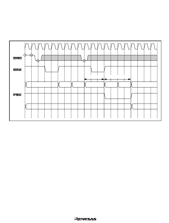
Rev. 2.0, 04/02, page 377 of 906
If a transfer request is generated for another channel, an EXDMA cycle for the other channel is
generated before the next EXDMA cycle.
The
('5(4 pin sensing timing is different for low level sensing and falling edge sensing. The
same applies to transfer request acceptance and transfer start timing.
Figures 8.35 to 8.38 show operation timing examples for various conditions.
¯ pin
Bus cycle
EDA bit
Bus release
Bus release
Bus release
EXDMA
read
EXDMA
write
EXDMA
read
EXDMA
write
0
1
Last transfer cycle
3 cycles
Figure 8.35 External Request/Cycle Steal Mode/Normal Transfer Mode
(No Contention/Dual Address Mode/Low Level Sensing)
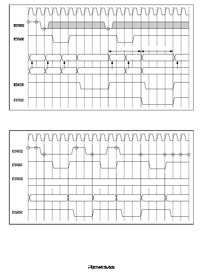
Rev. 2.0, 04/02, page 378 of 906
¯ pin
Bus cycle
CPU
operation
Last transfer cycle
2 bus cycles
CPU cycle
External
space
External
space
External
space
External
space
External
space
External
space
EXDMA single
transfer cycle
EXDMA single
transfer cycle
CPU cycle CPU cycle
CPU cycle
CPU cycle
CPU cycle
Figure 8.36 External Request/Cycle Steal Mode/Normal Transfer Mode
(CPU Cycles/Single Address Mode/Low Level Sensing)
¯ pin
Bus cycle
acceptance
internal
processing
state
Bus release
Bus release
Bus release
Start of high
level sensing
Start of high
level sensing
Start of high
level sensing
EXDMA single
transfer cycle
EXDMA single
transfer cycle
EXDMA single
transfer cycle
Edge confirmation
Start of transfer
processing
Edge confirmation
Start of transfer
processing
Edge confirmation
Start of transfer
processing
Figure 8.37 External Request/Cycle Steal Mode/Normal Transfer Mode
(No Contention/Single Address Mode/Falling Edge Sensing)
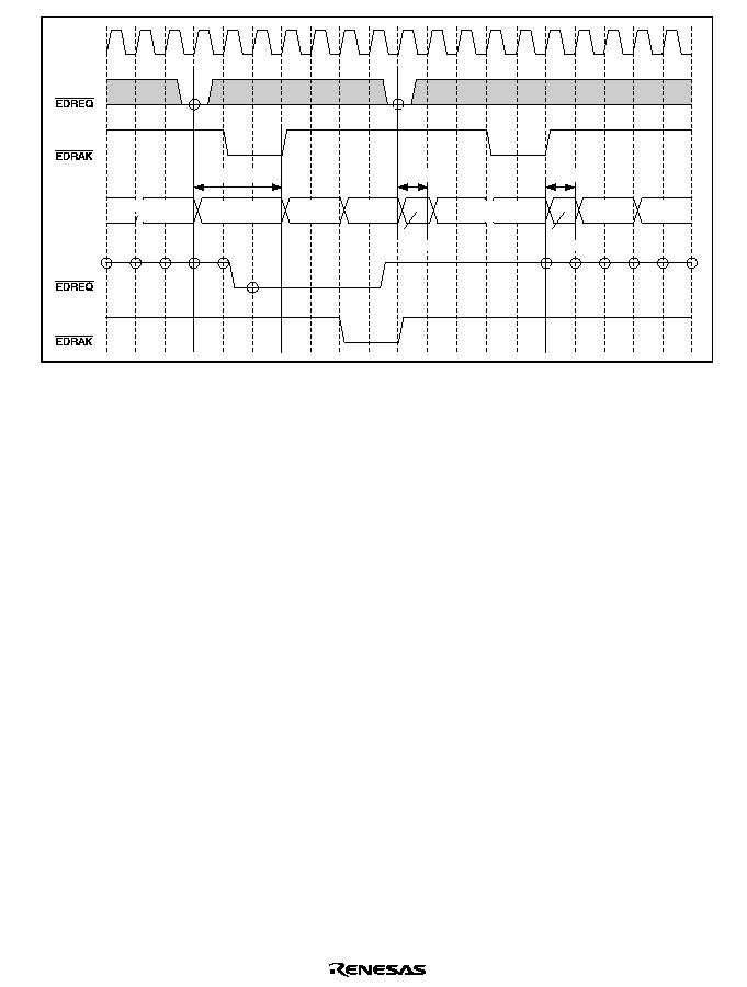
Rev. 2.0, 04/02, page 379 of 906
¯ pin
Original
channel
Original
channel
Other
channel
Other
channel
Bus cycle
3 cycles
1 cycle
1 cycle
EXDMA transfer
cycle
Bus release
Other channel
transfer cycle
EXDMA
read
EXDMA
write
EXDMA
read
EXDMA
write
Bus
release
Bus
release
Figure 8.38 External Request/Cycle Steal Mode/Normal Transfer Mode Contention
with Another Channel/Dual Address Mode/Low Level Sensing
External Request/Cycle Steal Mode/Block Transfer Mode: In block transfer mode, transfer of
one block is performed continuously in the same way as in burst mode. The timing of the start of
the next block transfer is the same as in normal transfer mode.
If a transfer request is generated for another channel, an EXDMA cycle for the other channel is
generated before the next block transfer.
The
('5(4 pin sensing timing is different for low level sensing and falling edge sensing. The
same applies to transfer request acceptance and transfer start timing.
Figures 8.39 to 8.44 show operation timing examples for various conditions.
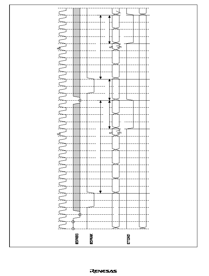
Rev. 2.0, 04/02, page 380 of 906
¯ pin
Bus cycle
EDA bit
Bus release
Bus release
EXDMA
read
EXDMA
write
EXDMA
read
EXDMA
write
EXDMA
read
EXDMA
write
EXDMA
read
EXDMA
write
EXDMA
read
EXDMA
write
0
1
Last transfer
in block
1-block-size transfer period
Last block
Last transfer cycle
3 cycles
Repeated
Bus release
Repeated
Figure 8.39 External Request/Cycle Steal Mode/Block Transfer Mode
(No Contention/Dual Address Mode/Low Level Sensing/BGUP = 0)
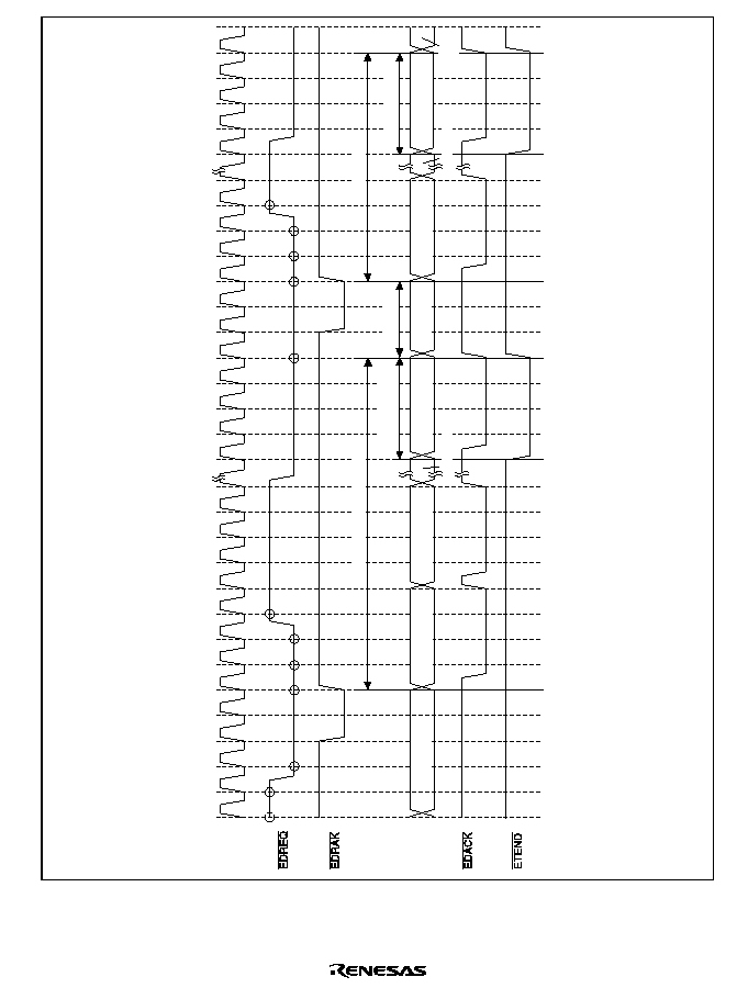
Rev. 2.0, 04/02, page 381 of 906
¯ pin
Bus cycle
Bus release
Bus release
Last transfer
in block
1-block-size transfer period
Last block
Last transfer cycle
3 cycles
EXDMA single
transfer cycle
EXDMA single
transfer cycle
EXDMA single
transfer cycle
EXDMA single
transfer cycle
EXDMA single
transfer cycle
Repeated
Repeated
Bus release
Figure 8.40 External Request/Cycle Steal Mode/Block Transfer Mode
(No Contention/Single Address Mode/Falling Edge Sensing/BGUP = 0)

Rev. 2.0, 04/02, page 382 of 906
¯ pin
Bus cycle
CPU
operation
1-block-size transfer period
1-block-size transfer period
Last transfer
in block
Last transfer
in block
2 bus cycles
EXDMA single
transfer cycle
EXDMA single
transfer cycle
EXDMA single
transfer cycle
EXDMA single
transfer cycle
External
space
External
space
External
space
External
space
External
space
CPU cycle
CPU cycle
CPU cycle
CPU cycle
CPU cycle
CPU cycle
External
space
Repeated
Repeated
Figure 8.41 External Request/Cycle Steal Mode/Block Transfer Mode
(CPU Cycles/Single Address Mode/Low Level Sensing/BGUP = 0)
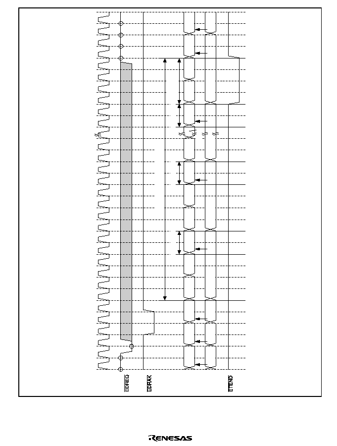
Rev. 2.0, 04/02, page 383 of 906
¯ pin
Bus cycle
CPU
operation
1-block-size transfer period
1 bus cycle
CPU cycle
CPU cycle
CPU cycle
CPU cycle
CPU cycle
CPU cycle
CPU cycle
CPU cycle
External
space
External
space
External
space
External
space
EXDMA
read
EXDMA
write
EXDMA
read
EXDMA
read
EXDMA
write
EXDMA
read
EXDMA
write
1 bus cycle
1 bus cycle
Last transfer
in block
External
space
External
space
External
space
External
space
Repeated
Figure 8.42 External Request/Cycle Steal Mode/Block Transfer Mode
(CPU Cycles/Dual Address Mode/Low Level Sensing/BGUP = 1)
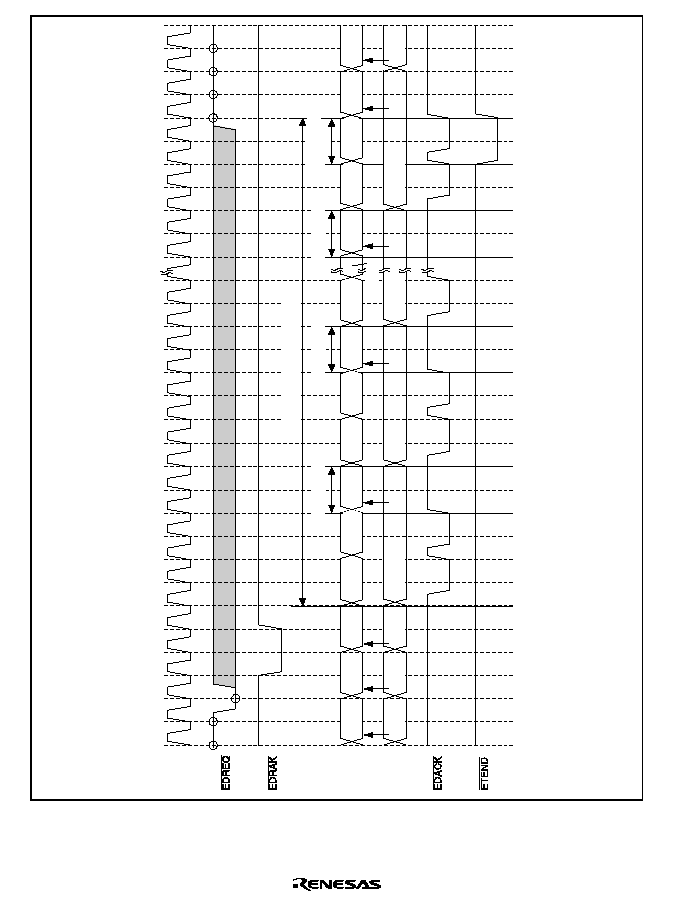
Rev. 2.0, 04/02, page 384 of 906
¯ pin
Bus cycle
CPU
operation
1-block-size transfer period
1 bus cycle
CPU cycle
CPU cycle
External
space
External
space
CPU cycle
CPU cycle
CPU cycle
CPU cycle
CPU cycle
CPU cycle
External
space
External
space
External
space
External
space
External
space
External space
1 bus cycle
1 bus cycle
Last transfer
in block
EXDMA
transfer cycle
EXDMA
transfer cycle
EXDMA
transfer cycle
EXDMA
transfer cycle
EXDMA
transfer cycle
EXDMA
transfer cycle
EXDMA
transfer cycle
Repeated
Figure 8.43 External Request/Cycle Steal Mode/Block Transfer Mode
(CPU Cycles/Single Address Mode/Low Level Sensing/BGUP = 1)
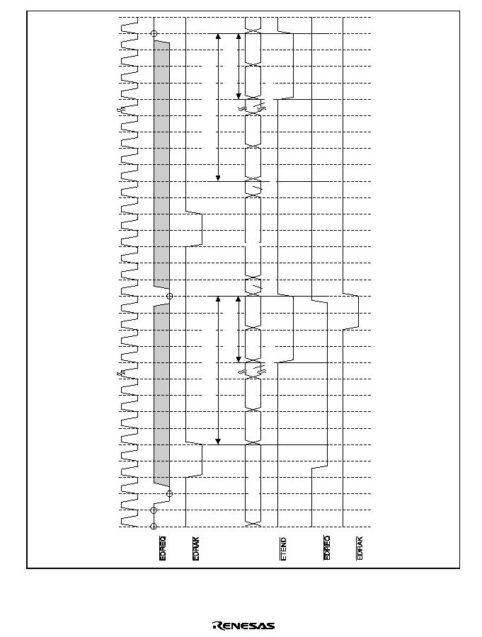
Rev. 2.0, 04/02, page 385 of 906
¯ pin
Bus cycle
Other
channel
Other
channel
Bus release
EXDMA
read
EXDMA
write
EXDMA
read
EXDMA
write
EXDMA
read
EXDMA
write
EXDMA
read
EXDMA
write
Last transfer
in block
Last transfer
in block
1-block-size transfer period
1-block-size transfer period
Other channel EXDMA cycle
Bus release
Bus release
Repeated
Repeated
Figure 8.44 External Request/Cycle Steal Mode/Block Transfer Mode
(Contention with Another Channel/Dual Address Mode/Low Level Sensing)

Rev. 2.0, 04/02, page 386 of 906
8.4.12
Ending DMA Transfer
The operation for ending DMA transfer depends on the transfer end conditions. When DMA
transfer ends, the EDA bit in EDMDR changes from 1 to 0, indicating that DMA transfer has
ended.
Transfer End by 1
0 Transition of EDTCR: When the value of EDTCR changes from 1 to 0,
DMA transfer ends on the corresponding channel and the EDA bit in EDMDR is cleared to 0. If
the TCEIE bit in EDMDR is set at this time, a transfer end interrupt request is generated by the
transfer counter and the IRF bit in EDMDR is set to 1.
In block transfer mode, DMA transfer ends when the value of bits 15 to 0 in EDTCR changes
from 1 to 0.
DMA transfer does not end if the EDTCR value has been 0 since before the start of transfer.
Transfer End by Repeat Area Overflow Interrupt: If an address overflows the repeat area
when a repeat area specification has been made and repeat interrupts have been enabled (with the
SARIE or DARIE bit in EDACR), a repeat area overflow interrupt is requested. DMA transfer
ends, the EDA bit in EDMDR is cleared to 0, and the IRF bit in EDMDR is set to 1.
In dual address mode, if a repeat area overflow interrupt is requested during a read cycle, the
following write cycle processing is still executed.
In block transfer mode, if a repeat area overflow interrupt is requested during transfer of a block,
transfer continues to the end of the block. Transfer end by means of a repeat area overflow
interrupt occurs between block-size transfers.
Transfer End by 0-Write to EDA Bit in EDMDR: When 0 is written to the EDA bit in EDMDR
by the CPU, etc., transfer ends after completion of the DMA cycle in which transfer is in progress
or a transfer request was accepted.
In block transfer mode, DMA transfer halts after completion of one-block-size transfer.
The EDA bit in EDMDR is not cleared to 0 until all transfer processing has ended. Up to that
point, the value of the EDA bit will be read as 1.
Transfer Abort by NMI Interrupt: DMA transfer is aborted when an NMI interrupt is
generated. The EDA bit is cleared to 0 in all channels. In external request mode, DMA transfer is
performed for all transfer requests for which
('5$. has been output. In dual address mode,
processing is executed for the write cycle following the read cycle.
In block transfer mode, operation is aborted even in the middle of a block-size transfer. As the
transfer is halted midway through a block, the BEF bit in EDMDR is set to 1 to indicate that the
block transfer was not carried out normally.

Rev. 2.0, 04/02, page 387 of 906
When transfer is aborted, register values are retained, and as the address registers indicate the next
transfer addresses, transfer can be resumed by setting the EDA bit to 1 in EDMDR. If the BEF bit
is 1 in EDMDR, transfer can be resumed from midway through a block.
Hardware Standby Mode and Reset Input: The EXDMAC is initialized in hardware standby
mode and by a reset. DMA transfer is not guaranteed in these cases.
8.4.13
Relationship between EXDMAC and Other Bus Masters
The read and write operations in a DMA transfer cycle are indivisible, and a refresh cycle, external
bus release cycle, or internal bus mastership (CPU, DTC, or DMAC) external space access cycle
never occurs between the two.
When read and write cycles occur consecutively, as in burst transfer or block transfer, a refresh or
external bus release state may be inserted after the write cycle. As the internal bus masters are of
lower priority than the EXDMAC, external space accesses by internal bus masters are not
executed until the EXDMAC releases the bus.
The EXDMAC releases the bus in the following cases:
1. When DMA transfer is performed in cycle steal mode
2. When switching to a different channel
3. When transfer ends in burst transfer mode
4. When transfer of one block ends in block transfer mode
5. When burst transfer or block transfer is performed with the BGUP bit in EDMDR set to 1
(however, the bus is not released between read and write cycles)
8.5
Interrupt Sources
EXDMAC interrupt sources are a transfer end indicated by the transfer counter, and repeat area
overflow interrupts. Table 8.4 shows the interrupt sources and their priority order.

Rev. 2.0, 04/02, page 388 of 906
Table 8.4
Interrupt Sources and Priority Order
Interrupt
Interrupt source
Interrupt Priority
EXDMTEND0
Transfer end indicated by channel 0 transfer counter
Channel 0 source address repeat area overflow
Channel 0 destination address repeat area overflow
High
EXDMTEND1
Transfer end indicated by channel 1 transfer counter
Channel 1 source address repeat area overflow
Channel 1 destination address repeat area overflow
EXDMTEND2
Transfer end indicated by channel 2 transfer counter
Channel 2 source address repeat area overflow
Channel 2 destination address repeat area overflow
EXDMTEND3
Transfer end indicated by channel 3 transfer counter
Channel 3 source address repeat area overflow
Channel 3 destination address repeat area overflow
Low
Interrupt sources can be enabled or disabled by means of the EDIE bit in EDMDR for the relevant
channel, and can be sent to the interrupt controller independently. The relative priority order of the
channels is determined by the interrupt controller (see table 8.4).
Figure 8.45 shows the transfer end interrupt logic. A transfer end interrupt is generated whenever
the EDIE bit is set to 1 while the IRF bit is set to 1 in EDMDR.
Transfer end interrupt
IRF bit
EDIE bit
Figure 8.45 Transfer End Interrupt Logic
Interrupt source settings are made individually with the interrupt enable bits in the registers for the
relevant channels. The transfer counter's transfer end interrupt is enabled or disabled by means of
the TCEIE bit in EDMDR, the source address register repeat area overflow interrupt by means of
the SARIE bit in EDACR, and the destination address register repeat area overflow interrupt by
means of the DARIE bit in EDACR. When an interrupt source occurs while the corresponding
interrupt enable bit is set to 1, the IRF bit in EDMDR is set to 1. The IRF bit is set by all interrupt
sources indiscriminately.
The transfer end interrupt can be cleared either by clearing the IRF bit to 0 in EDMDR within the
interrupt handling routine, or by re-setting the transfer counter and address registers and then
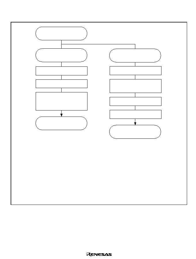
Rev. 2.0, 04/02, page 389 of 906
setting the EDA bit to 1 in EDMDR to perform transfer continuation processing. An example of
the procedure for clearing the transfer end interrupt and restarting transfer is shown in figure 8.46.
[1] Write set values to the registers (transfer counter, address registers, etc.).
[2] Write 1 to the EDA bit in EDMDR to restart EXDMA operation. When 1 is written to the EDA
bit, the IRF bit in EDMDR is automatically cleared to 0 and the interrupt source is cleared.
[3] The interrupt handling routine is ended with an RTE instruction, etc.
[4] Clear the IRF bit to 0 in EDMDR by first reading 1 from it, then writing 0.
[5] After the interrupt handling routine is ended with an RTE instruction, etc., interrupt masking is
cleared.
[6] Write set values to the registers (transfer counter, address registers, etc.).
[7] Write 1 to the EDA bit in EDMDR to restart EXDMA operation.
End of transfer restart
processing
Write 1 to EDA bit
Change register settings
End of interrupt handling
routine
Clear IRF bit to 0
Transfer restart after end
of interrupt handling routine
Transfer end interrupt
exception handling routine
Transfer continuation
processing
Change register settings
Write 1 to EDA bit
End of interrupt handling
routine
(RTE instruction execution)
End of transfer restart
processing
[1]
[4]
[5]
[6]
[7]
[2]
[3]
Figure 8.46 Example of Procedure for Restarting Transfer on Channel in which Transfer
End Interrupt Occurred

Rev. 2.0, 04/02, page 390 of 906
8.6
Usage Notes
8.6.1
EXDMAC Register Access during Operation
Except for clearing the EDA bit to 0 in EDMDR, settings should not be changed for a channel in
operation (including the transfer standby state). Transfer must be disabled before changing a
setting for an operational channel.
8.6.2
Module Stop State
When the MSTP14 bit is set to 1 in MSTPCRH, the EXDMAC clock stops and the EXDMAC
enters the module stop state. However, 1 cannot be written to the MSTP14 bit when any of the
EXDMAC's channels is enabled for transfer, or when an interrupt is being requested. Before
setting the MSTP14 bit, first clear the EDA bit in EDMDR to 0, then clear the IRF or EDIE bit in
EDMDR to 0.
When the EXDMAC clock stops, EXDMAC registers can no longer be accessed. The following
EXDMAC register settings remain valid in the module stop state, and so should be changed, if
necessary, before making the module stop transition.
∑
ETENDE = 1 in EDMDR (
(7(1' pin enable)
∑
EDRAKE = 1 in EDMDR (
('5$. pin enable)
∑
AMS = 1 in EDMDR (
('$&. pin enable)
8.6.3
#"
#" Pin Falling Edge Activation
Falling edge sensing on the
('5(4 pin is performed in synchronization with EXDMAC internal
operations, as indicated below.
[1] Activation request standby state: Waits for low level sensing on
('5(4 pin, then goes to [2].
[2] Transfer standby state: Waits for EXDMAC data transfer to become possible, then goes to [3].
[3] Activation request disabled state: Waits for high level sensing on
('5(4 pin, then goes to [1].
After EXDMAC transfer is enabled, the EXDMAC goes to state [1], so low level sensing is used
for the initial activation after transfer is enabled.
8.6.4
Activation Source Acceptance
At the start of activation source acceptance, low level sensing is used for both falling edge sensing
and low level sensing on the
('5(4 pin. Therefore, a request is accepted in the case of a low
level at the
('5(4 pin that occurs before execution of the EDMDR write for setting the transfer-
enabled state.

Rev. 2.0, 04/02, page 391 of 906
When the EXDMAC is activated, make sure, if necessary, that a low level does not remain at the
('5(4 pin from the previous end of transfer, etc.
8.6.5
Enabling Interrupt Requests when IRF = 1 in EDMDR
When transfer is started while the IRF bit is set to 1 in EDMDR, if the EDIE bit is set to 1 in
EDMDR together with the EDA bit in EDMDR, enabling interrupt requests, an interrupt will be
requested since EDIE = 1 and IRF = 1. To prevent the occurrence of an erroneous interrupt request
when transfer starts, ensure that the IRF bit is cleared to 0 before the EDIE bit is set to 1.
8.6.6
%
%
Pin and CBR Refresh Cycle
If the last EXDMAC transfer cycle and a CBR refresh cycle occur simultaneously, note that
although the CBR refresh and the last transfer cycle may be executed consecutively,
(7(1' may
also go low in this case for the refresh cycle.

Rev. 2.0, 04/02, page 392 of 906

Rev. 2.0, 04/02, page 393 of 906
Section 9 Data Transfer Controller (DTC)
This LSI includes a data transfer controller (DTC). The DTC can be activated by an interrupt or
software, to transfer data.
Figure 9.1 shows a block diagram of the DTC. The DTC's register information is stored in the on-
chip RAM. When the DTC is used, the RAME bit in SYSCR must be set to 1. A 32-bit bus
connects the DTC to the on-chip RAM (1 kbyte), enabling 32-bit/1-state reading and writing of
the DTC register information.
9.1
Features
∑
Transfer possible over any number of channels
∑
Three transfer modes
Normal, repeat, and block transfer modes available
∑
One activation source can trigger a number of data transfers (chain transfer)
∑
Direct specification of 16-Mbyte address space possible
∑
Activation by software is possible
∑
Transfer can be set in byte or word units
∑
A CPU interrupt can be requested for the interrupt that activated the DTC
∑
Module stop mode can be set
DTCH804A_010020020400
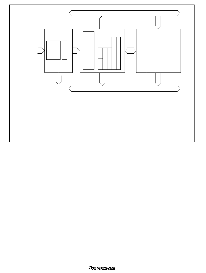
Rev. 2.0, 04/02, page 394 of 906
Interrupt
request
Interrupt controller
DTC
Internal address bus
DTC activation
request
Control logic
Register information
MRA
MRB
CRA
CRB
DAR
SAR
CPU interrupt
request
On-chip
RAM
Internal data bus
Legend
MRA, MRB
CRA, CRB
SAR
DAR
DTCERA to DTCERG
DTVECR
DTCERA
to
DTCERG
DTVECR
: DTC mode registers A and B
: DTC transfer count registers A and B
: DTC source address register
: DTC destination address register
: DTC enable registers A to G
: DTC vector register
Figure 9.1 Block Diagram of DTC
9.2
Register Descriptions
DTC has the following registers.
∑
DTC mode register A (MRA)
∑
DTC mode register B (MRB)
∑
DTC source address register (SAR)
∑
DTC destination address register (DAR)
∑
DTC transfer count register A (CRA)
∑
DTC transfer count register B (CRB)
These six registers cannot be directly accessed from the CPU. When activated, the DTC reads a set
of register information that is stored in an on-chip RAM to the corresponding DTC registers and
transfers data. After the data transfer, it writes a set of updated register information back to the
RAM.
∑
DTC enable registers A to G (DTCERA to DTCERG)

Rev. 2.0, 04/02, page 395 of 906
∑
DTC vector register (DTVECR)
9.2.1
DTC Mode Register A (MRA)
MRA selects the DTC operating mode.
Bit
Bit Name
Initial Value
R/W
Description
7
6
SM1
SM0
Undefined
Undefined
-
-
Source Address Mode 1 and 0
These bits specify an SAR operation after a data
transfer.
0x: SAR is fixed
10: SAR is incremented after a transfer
(by +1 when Sz = 0; by +2 when Sz = 1)
11: SAR is decremented after a transfer
(by ≠1 when Sz = 0; by ≠2 when Sz = 1)
5
4
DM1
DM0
Undefined
Undefined
-
-
Destination Address Mode 1 and 0
These bits specify a DAR operation after a data
transfer.
0x: DAR is fixed
10: DAR is incremented after a transfer
(by +1 when Sz = 0; by +2 when Sz = 1)
11: DAR is decremented after a transfer
(by ≠1 when Sz = 0; by ≠2 when Sz = 1)
3
2
MD1
MD0
Undefined
Undefined
-
-
DTC Mode
These bits specify the DTC transfer mode.
00: Normal mode
01: Repeat mode
10: Block transfer mode
11: Setting prohibited
1
DTS
Undefined
-
DTC Transfer Mode Select
Specifies whether the source side or the destination
side is set to be a repeat area or block area, in repeat
mode or block transfer mode.
0: Destination side is repeat area or block area
1: Source side is repeat area or block area

Rev. 2.0, 04/02, page 396 of 906
Bit
Bit Name
Initial Value
R/W
Description
0
Sz
Undefined
-
DTC Data Transfer Size
Specifies the size of data to be transferred.
0: Byte-size transfer
1: Word-size transfer
Legend:
X : Don't care
9.2.2
DTC Mode Register B (MRB)
MRB selects the DTC operating mode.
Bit
Bit Name
Initial Value
R/W
Description
7
CHNE
Undefined
-
DTC Chain Transfer Enable
When this bit is set to 1, a chain transfer will be
performed. For details, refer to 9.5.4, Chain Transfer.
In data transfer with CHNE set to 1, determination of
the end of the specified number of transfers, clearing
of the activation source flag, and clearing of DTCER
is not performed.
6
DISEL
Undefined
-
DTC Interrupt Select
When this bit is set to 1, a CPU interrupt request is
generated every time after a data transfer ends.
When this bit is set to 0, a CPU interrupt request is
generated at the time when the specified number of
data transfer ends.
5
CHNS
Undefined
-
DTC Chain Transfer Select
Specifies the chain transfer condition.
0: Chain transfer every time
1: Chain transfer only when transfer counter = 0
4
to
0
-
Undefined
-
Reserved
These bits have no effect on DTC operation, and
should always be written with 0.
9.2.3
DTC Source Address Register (SAR)
SAR is a 24-bit register that designates the source address of data to be transferred by the DTC.
For word-size transfer, specify an even source address.

Rev. 2.0, 04/02, page 397 of 906
9.2.4
DTC Destination Address Register (DAR)
DAR is a 24-bit register that designates the destination address of data to be transferred by the
DTC. For word-size transfer, specify an even destination address.
9.2.5
DTC Transfer Count Register A (CRA)
CRA is a 16-bit register that designates the number of times data is to be transferred by the DTC.
In normal mode, the entire CRA functions as a 16-bit transfer counter (1 to 65,536). It is
decremented by 1 every time data is transferred, and transfer ends when the count reaches H'0000.
In repeat mode or block transfer mode, the CRA is divided into two parts: the upper 8 bits
(CRAH) and the lower 8 bits (CRAL). CRAH holds the number of transfers while CRAL
functions as an 8-bit transfer counter (1 to 256). CRAL is decremented by 1 every time data is
transferred, and the contents of CRAH are sent when the count reaches H'00.
9.2.6
DTC Transfer Count Register B (CRB)
CRB is a 16-bit register that designates the number of times data is to be transferred by the DTC in
block transfer mode. It functions as a 16-bit transfer counter (1 to 65,536) that is decremented by 1
every time data is transferred, and transfer ends when the count reaches H'0000. This register is
not available in normal and repeat modes.
9.2.7
DTC Enable Registers A to G (DTCERA to DTCERG)
DTCER which is comprised of seven registers, DTCERA to DTCERG, is a register that specifies
DTC activation interrupt sources. The correspondence between interrupt sources and DTCE bits is
shown in table 9.1. For DTCE bit setting, use bit manipulation instructions such as BSET and
BCLR for reading and writing. If all interrupts are masked, multiple activation sources can be set
at one time (only at the initial setting) by writing data after executing a dummy read on the
relevant register.

Rev. 2.0, 04/02, page 398 of 906
Bit
Bit Name
Initial Value
R/W
Description
7
6
5
4
3
2
1
0
DTCE7
DTCE6
DTCE5
DTCE4
DTCE3
DTCE2
DTCE1
DTCE0
0
0
0
0
0
0
0
0
R/W
R/W
R/W
R/W
R/W
R/W
R/W
R/W
DTC Activation Enable
Setting this bit to 1 specifies a relevant interrupt
source to a DTC activation source.
[Clearing conditions]
∑
When the DISEL bit is 1 and the data transfer has
ended
∑
When the specified number of transfers have
ended
These bits are not cleared when the DISEL bit is 0
and the specified number of transfers have not ended
9.2.8
DTC Vector Register (DTVECR)
DTVECR enables or disables DTC activation by software, and sets a vector number for the
software activation interrupt.
Bit
Bit Name
Initial Value
R/W
Description
7
SWDTE
0
R/W
DTC Software Activation Enable
Setting this bit to 1 activates DTC. Only 1 can be
written to this bit.
[Clearing conditions]
∑
When the DISEL bit is 0 and the specified
number of transfers have not ended
∑
When 0 is written to the DISEL bit after a
software-activated data transfer end interrupt
(SWDTEND) request has been sent to the CPU.
When the DISEL bit is 1 and data transfer has ended
or when the specified number of transfers have
ended, this bit will not be cleared.
6
5
4
3
2
1
0
DTVEC6
DTVEC5
DTVEC4
DTVEC3
DTVEC2
DTVEC1
DTVEC0
0
0
0
0
0
0
0
R/W
R/W
R/W
R/W
R/W
R/W
R/W
DTC Software Activation Vectors 6 to 0
These bits specify a vector number for DTC software
activation.
The vector address is expressed as H'0400 + (vector
number
◊
2). For example, when DTVEC6 to
DTVEC0 = H'10, the vector address is H'0420. When
the bit SWDTE is 0, these bits can be written.
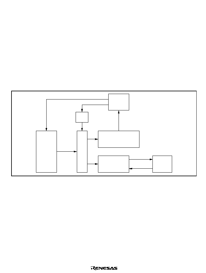
Rev. 2.0, 04/02, page 399 of 906
9.3
Activation Sources
The DTC operates when activated by an interrupt or by a write to DTVECR by software. An
interrupt request can be directed to the CPU or DTC, as designated by the corresponding DTCER
bit. At the end of a data transfer (or the last consecutive transfer in the case of chain transfer), the
activation source or corresponding DTCER bit is cleared. The activation source flag, in the case
of RXI0, for example, is the RDRF flag of SCI_0.
When an interrupt has been designated a DTC activation source, existing CPU mask level and
interrupt controller priorities have no effect. If there is more than one activation source at the same
time, the DTC operates in accordance with the default priorities.
Figure 9.2 shows a block diagram of activation source control. For details see section 5, Interrupt
Controller.
CPU
DTC
DTCER
Source flag cleared
On-chip
supporting
module
IRQ interrupt
Interrupt
request
Clear
Clear
controller
Clear request
Interrupt controller
Selection circuit
Interrupt mask
Select
DTVECR
Figure 9.2 Block Diagram of DTC Activation Source Control
9.4
Location of Register Information and DTC Vector Table
Locate the register information in the on-chip RAM (addresses: H'FFBC00 to H'FFBFFF).
Register information should be located at the address that is multiple of four within the range.
Locating the register information in address space is shown in figure 9.3. Locate the MRA, SAR,
MRB, DAR, CRA, and CRB registers, in that order, from the start address of the register
information. In the case of chain transfer, register information should be located in consecutive
areas as shown in figure 9.3 and the register information start address should be located at the
corresponding vector address to the activation source. The DTC reads the start address of the
register information from the vector address set for each activation source, and then reads the
register information from that start address.

Rev. 2.0, 04/02, page 400 of 906
When the DTC is activated by software, the vector address is obtained from: H'0400 +
(DTVECR[6:0]
◊
2). For example, if DTVECR is H'10, the vector address is H'0420.
The configuration of the vector address is the same in both normal* and advanced modes, a 2-byte
unit being used in both cases. These two bytes specify the lower bits of the register information
start address.
MRA
Start address of
register information
Register information
Register information
for second transfer
in case of chain
transfer
Chain transfer
Lower addresses
Four bytes
0
1
2
3
SAR
MRB
DAR
CRA
CRB
MRA
SAR
MRB
DAR
CRA
CRB
Figure 9.3 Correspondence between DTC Vector Address and Register Information
Note:
Not available in this LSI.

Rev. 2.0, 04/02, page 401 of 906
Table 9.1
Interrupt Sources, DTC Vector Addresses, and Corresponding DTCEs
Origin of
Activation
Source
Activation
Source
Vector Number
DTC
Vector Address
DTCE
*
Priority
Software
Write to DTVECR
DTVECR
H'0400 + (DTVECR
[
6:0
]
◊
2)
--
High
External pin
IRQ0
16
H'0420
DTCEA7
IRQ1
17
H'0422
DTCEA6
IRQ2
18
H'0424
DTCEA5
IRQ3
19
H'0426
DTCEA4
IRQ4
20
H'0428
DTCEA3
IRQ5
21
H'042A
DTCEA2
IRQ6
22
H'042C
DTCEA1
IRQ7
23
H'042E
DTCEA0
IRQ8
24
H'0430
DTCEB7
IRQ9
25
H'0432
DTCEB6
IRQ10
26
H'0434
DTCEB5
IRQ11
17
H'0436
DTCEB4
IRQ12
18
H'0438
DTCEB3
IRQ13
19
H'043A
DTCEB2
IRQ14
30
H'043C
DTCEB1
IRQ15
31
H'043E
DTCEB0
A/D
ADI
38
H'044C
DTCEC6
TPU_0
TGI0A
40
H'0450
DTCEC5
TGI0B
41
H'0452
DTCEC4
TGI0C
42
H'0454
DTCEC3
TGI0D
43
H'0456
DTCEC2
TPU_1
TGI1A
48
H'0460
DTCEC1
TGI1B
49
H'0462
DTCEC0
TPU_2
TGI2A
52
H'0468
DTCED7
TGI2B
53
H'046A
DTCED6
TPU_3
TGI3A
56
H'0470
DTCED5
TGI3B
57
H'0472
DTCED4
TGI3C
58
H'0474
DTCED3
TGI3D
59
H'0476
DTCED2
TPU_4
TGI4A
64
H'0480
DTCED1
TGI4B
65
H'0482
DTCED0
TPU_5
TGI5A
68
H'0488
DTCEE7
TGI5B
69
H'048A
DTCEE6
Low

Rev. 2.0, 04/02, page 402 of 906
Origin of
Activation
Source
Activation
Source
Vector Number
DTC
Vector Address
DTCE
*
Priority
TMR_0
CMIA0
72
H'0490
DTCEE3
High
CMIB0
73
H'0492
DTCEE2
TMR_1
CMIA1
76
H'0498
DTCEE1
CMIB1
77
H'049A
DTCEE0
DMAC
DMTEND0A
80
H'04A0
DTCEF7
DMTEND0B
81
H'04A2
DTCEF6
DMTEND1A
82
H'04A4
DTCEF5
DMTEND1B
83
H'04A6
DTCEF4
SCI_0
RXI0
89
H'04B2
DTCEF3
TXI0
90
H'04B4
DTCEF2
SCI_1
RXI1
93
H'04BA
DTCEF1
TXI1
94
H'04BC
DTCEF0
SCI_2
RXI2
97
H'04C2
DTCEG7
TXI2
98
H'04C4
DTCEG6
Low
Note: DTCE bits with no corresponding interrupt are reserved, and should be written with 0.
When clearing the software standby state or all-module-clocks-stop mode with an interrupt,
write 0 to the corresponding DTCE bit.
9.5
Operation
The DTC stores register information in the on-chip RAM. When activated, the DTC reads register
information that is already stored in the on-chip RAM and transfers data on the basis of that
register information. After the data transfer, it writes updated register information back to the on-
chip RAM. Pre-storage of register information in the on-chip RAM makes it possible to transfer
data over any required number of channels. There are three transfer modes: normal mode, repeat
mode, and block transfer mode. Setting the CHNE bit to 1 makes it possible to perform a number
of transfers with a single activation (chain transfer). A setting can also be made to have chain
transfer performed only when the transfer counter value is 0. This enables DTC re-setting to be
performed by the DTC itself.
The 24-bit SAR designates the DTC transfer source address and the 24-bit DAR designates the
transfer destination address. After each transfer, SAR and DAR are independently incremented,
decremented, or left fixed.
Figure 9.4 shows a flowchart of DTC operation, and table 9.2 summarizes the chain transfer
conditions (combinations for performing the second and third transfers are omitted).

Rev. 2.0, 04/02, page 403 of 906
Start
Read DTC vector
Next transfer
Read register information
Data transfer
Write register information
Clear activation flag
CHNE = 1?
End
No
No
No
No
No
Yes
Yes
Yes
Yes
Yes
Transfer counter = 0
or DISEL = 1?
Clear DTCER
Interrupt exception
handling
CHNS = 0?
DISEL = 1?
Transfer
counter = 0?
Figure 9.4 Flowchart of DTC Operation

Rev. 2.0, 04/02, page 404 of 906
Table 9.2
Chain Transfer Conditions
1st Transfer
2nd Transfer
CHNE
CHNS
DISEL
CR
CHNE
CHNS
DISEL
CR
DTC Transfer
0
--
0
Not 0
--
--
--
--
Ends at 1st transfer
0
--
0
0
--
--
--
--
Ends at 1st transfer
0
--
1
--
--
--
--
--
Interrupt request to CPU
1
0
--
--
0
--
0
Not 0
Ends at 2nd transfer
0
--
0
0
Ends at 2nd transfer
0
--
1
--
Interrupt request to CPU
1
1
0
Not 0
--
--
--
--
Ends at 1st transfer
1
1
--
0
0
--
0
Not 0
Ends at 2nd transfer
0
--
0
0
Ends at 2nd transfer
0
--
1
--
Interrupt request to CPU
1
1
1
Not 0
--
--
--
--
Ends at 1st transfer
Interrupt request to CPU
9.5.1
Normal Mode
In normal mode, one operation transfers one byte or one word of data. Table 9.3 lists the register
function in normal mode. From 1 to 65,536 transfers can be specified. Once the specified number
of transfers has ended, a CPU interrupt can be requested.
Table 9.3
Register Function in Normal Mode
Name
Abbreviation
Function
DTC source address register
SAR
Designates source address
DTC destination address register
DAR
Designates destination address
DTC transfer count register A
CRA
Designates transfer count
DTC transfer count register B
CRB
Not used

Rev. 2.0, 04/02, page 405 of 906
SAR
DAR
Transfer
Figure 9.5 Memory Mapping in Normal Mode
9.5.2
Repeat Mode
In repeat mode, one operation transfers one byte or one word of data. Table 9.4 lists the register
function in repeat mode. From 1 to 256 transfers can be specified. Once the specified number of
transfers has ended, the initial state of the transfer counter and the address register specified as the
repeat area is restored, and transfer is repeated. In repeat mode the transfer counter value does not
reach H'00, and therefore CPU interrupts cannot be requested when DISEL = 0.
Table 9.4
Register Function in Repeat Mode
Name
Abbreviation
Function
DTC source address register
SAR
Designates source address
DTC destination address register
DAR
Designates destination address
DTC transfer count register AH
CRAH
Holds number of transfers
DTC transfer count register AL
CRAL
Designates transfer count
DTC transfer count register B
CRB
Not used

Rev. 2.0, 04/02, page 406 of 906
SAR
or
DAR
DAR
or
SAR
Repeat area
Transfer
Figure 9.6 Memory Mapping in Repeat Mode
9.5.3
Block Transfer Mode
In block transfer mode, one operation transfers one block of data. Either the transfer source or the
transfer destination is designated as a block area. Table 9.5 lists the register function in block
transfer mode.
The block size is 1 to 256. When the transfer of one block ends, the initial state of the block size
counter and the address register specified as the block area is restored. The other address register
is then incremented, decremented, or left fixed. From 1 to 65,536 transfers can be specified. Once
the specified number of transfers has ended, a CPU interrupt is requested.
Table 9.5
Register Function in Block Transfer Mode
Name
Abbreviation
Function
DTC source address register
SAR
Designates source address
DTC destination address register
DAR
Designates destination address
DTC transfer count register AH
CRAH
Holds block size
DTC transfer count register AL
CRAL
Designates block size count
DTC transfer count register B
CRB
Designates transfer count

Rev. 2.0, 04/02, page 407 of 906
First block
Transfer
Block area
Nth block
DAR
or
SAR
SAR
or
DAR
Figure 9.7 Memory Mapping in Block Transfer Mode
9.5.4
Chain Transfer
Setting the CHNE bit to 1 enables a number of data transfers to be performed consecutively in
response to a single transfer request. SAR, DAR, CRA, CRB, MRA, and MRB, which define data
transfers, can be set independently.
Figure 9.8 shows the operation of chain transfer. When activated, the DTC reads the register
information start address stored at the vector address, and then reads the first register information
at that start address. The CHNE bit in MRB is checked after the end of data transfer, if the value is
1, the next register information, which is located consecutively, is read and transfer is performed.
This operation is repeated until the end of data transfer of register information with CHNE = 0. It
is also possible, by setting both the CHNE bit and CHNS bit to 1, to specify execution of chain
transfer only when the transfer counter value is 0.
In the case of transfer with CHNE set to 1, an interrupt request to the CPU is not generated at the
end of the specified number of transfers or by setting of the DISEL bit to 1, and the interrupt
source flag for the activation source is not affected.
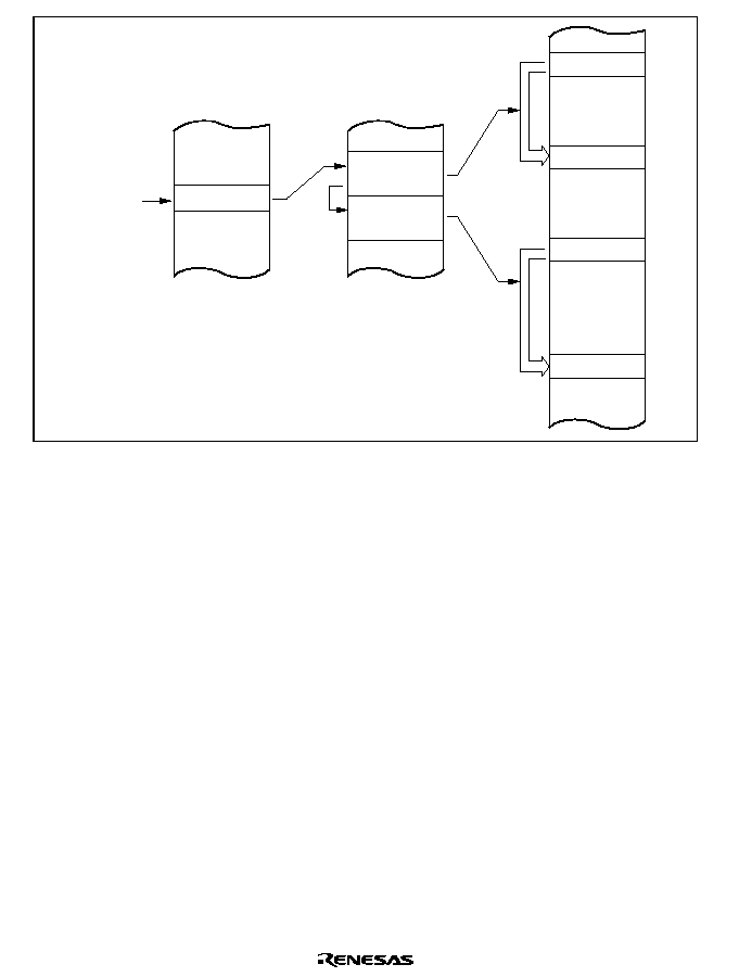
Rev. 2.0, 04/02, page 408 of 906
DTC vector
address
Register information
CHNE=1
Register information
CHNE=0
Register information
start address
Source
Destination
Source
Destination
Figure 9.8 Operation of Chain Transfer
9.5.5
Interrupt Sources
An interrupt request is issued to the CPU when the DTC finishes the specified number of data
transfers, or a data transfer for which the DISEL bit was set to 1. In the case of interrupt activation,
the interrupt set as the activation source is generated. These interrupts to the CPU are subject to
CPU mask level and interrupt controller priority level control.
In the case of activation by software, a software activated data transfer end interrupt (SWDTEND)
is generated.
When the DISEL bit is 1 and one data transfer has ended, or the specified number of transfers has
ended, after data transfer ends, the SWDTE bit is held at 1 and an SWDTEND interrupt is
generated. The interrupt handling routine should clear the SWDTE bit to 0.
When the DTC is activated by software, an SWDTEND interrupt is not generated during a data
transfer wait or during data transfer even if the SWDTE bit is set to 1.

Rev. 2.0, 04/02, page 409 of 906
9.5.6
Operation Timing
DTC activation
request
DTC
request
Address
Vector read
Read Write
Data transfer
Transfer
information write
Transfer
information read
Figure 9.9 DTC Operation Timing (Example in Normal Mode or Repeat Mode)
DTC activation
request
DTC
request
Address
Vector read
Read Write Read Write
Data transfer
Transfer
information write
Transfer
information read
Figure 9.10 DTC Operation Timing (Example of Block Transfer Mode,
with Block Size of 2)
DTC activation
request
DTC
request
Address
Vector read
Read Write
Read Write
Data transfer
Data transfer
Transfer
information
write
Transfer
information write
Transfer
information read
Transfer
information
read
Figure 9.11 DTC Operation Timing (Example of Chain Transfer)

Rev. 2.0, 04/02, page 410 of 906
9.5.7
Number of DTC Execution States
Table 9.6 lists execution status for a single DTC data transfer, and table 9.7 shows the number of
states required for each execution status.
Table 9.6
DTC Execution Status
Mode
Vector Read
I
Register Information
Read/Write
J
Data Read
K
Data Write
L
Internal
Operations
M
Normal
1
6
1
1
3
Repeat
1
6
1
1
3
Block transfer
1
6
N
N
3
Legend:
N: Block size (initial setting of CRAH and CRAL)
Table 9.7
Number of States Required for Each Execution Status
Object to be Accessed
On-
Chip
RAM
On-
Chip
ROM
On-Chip I/O
Registers
External Devices
Bus width
32
16
8
16
8
16
Access states
1
1
2
2
2
3
2
3
Execution
Vector read S
I
--
1
--
--
4
6+2m 2
3+m
status
Register information
read/write S
J
1
--
--
--
--
--
--
--
Byte data read S
K
1
1
2
2
2
3+m
2
3+m
Word data read S
K
1
1
4
2
4
6+2m 2
3+m
Byte data write S
L
1
1
2
2
2
3+m
2
3+m
Word data write S
L
1
1
4
2
4
6+2m 2
3+m
Internal operation S
M
1
The number of execution states is calculated from the formula below. Note that
means the sum
of all transfers activated by one activation event (the number in which the CHNE bit is set to 1,
plus 1).
Number of execution states = I ∑ S
I
+
(J ∑ S
J
+ K ∑ S
K
+ L ∑ S
L
) + M ∑ S
M
For example, when the DTC vector address table is located in on-chip ROM, normal mode is set,
and data is transferred from the on-chip ROM to an internal I/O register, the time required for the
DTC operation is 13 states. The time from activation to the end of the data write is 10 states.

Rev. 2.0, 04/02, page 411 of 906
9.6
Procedures for Using DTC
9.6.1
Activation by Interrupt
The procedure for using the DTC with interrupt activation is as follows:
1. Set the MRA, MRB, SAR, DAR, CRA, and CRB register information in the on-chip RAM.
2. Set the start address of the register information in the DTC vector address.
3. Set the corresponding bit in DTCER to 1.
4. Set the enable bits for the interrupt sources to be used as the activation sources to 1. The DTC
is activated when an interrupt used as an activation source is generated.
5. After the end of one data transfer, or after the specified number of data transfers have ended,
the DTCE bit is cleared to 0 and a CPU interrupt is requested. If the DTC is to continue
transferring data, set the DTCE bit to 1.
9.6.2
Activation by Software
The procedure for using the DTC with software activation is as follows:
1. Set the MRA, MRB, SAR, DAR, CRA, and CRB register information in the on-chip RAM.
2. Set the start address of the register information in the DTC vector address.
3. Check that the SWDTE bit is 0.
4. Write 1 to SWDTE bit and the vector number to DTVECR.
5. Check the vector number written to DTVECR.
6. After the end of one data transfer, if the DISEL bit is 0 and a CPU interrupt is not requested,
the SWDTE bit is cleared to 0. If the DTC is to continue transferring data, set the SWDTE bit
to 1. When the DISEL bit is 1, or after the specified number of data transfers have ended, the
SWDTE bit is held at 1 and a CPU interrupt is requested.
9.7
Examples of Use of the DTC
9.7.1
Normal Mode
An example is shown in which the DTC is used to receive 128 bytes of data via the SCI.
1. Set MRA to fixed source address (SM1 = SM0 = 0), incrementing destination address (DM1 =
1, DM0 = 0), normal mode (MD1 = MD0 = 0), and byte size (Sz = 0). The DTS bit can have
any value. Set MRB for one data transfer by one interrupt (CHNE = 0, DISEL = 0). Set the
SCI RDR address in SAR, the start address of the RAM area where the data will be received in
DAR, and 128 (H'0080) in CRA. CRB can be set to any value.
2. Set the start address of the register information at the DTC vector address.

Rev. 2.0, 04/02, page 412 of 906
3. Set the corresponding bit in DTCER to 1.
4. Set the SCI to the appropriate receive mode. Set the RIE bit in SCR to 1 to enable the reception
complete (RXI) interrupt. Since the generation of a receive error during the SCI reception
operation will disable subsequent reception, the CPU should be enabled to accept receive error
interrupts.
5. Each time reception of one byte of data ends on the SCI, the RDRF flag in SSR is set to 1, an
RXI interrupt is generated, and the DTC is activated. The receive data is transferred from RDR
to RAM by the DTC. DAR is incremented and CRA is decremented. The RDRF flag is
automatically cleared to 0.
6. When CRA becomes 0 after the 128 data transfers have ended, the RDRF flag is held at 1, the
DTCE bit is cleared to 0, and an RXI interrupt request is sent to the CPU. The interrupt
handling routine should perform wrap-up processing.
9.7.2
Chain Transfer
An example of DTC chain transfer is shown in which pulse output is performed using the PPG.
Chain transfer can be used to perform pulse output data transfer and PPG output trigger cycle
updating. Repeat mode transfer to the PPG's NDR is performed in the first half of the chain
transfer, and normal mode transfer to the TPU's TGR in the second half. This is because clearing
of the activation source and interrupt generation at the end of the specified number of transfers are
restricted to the second half of the chain transfer (transfer when CHNE = 0).
1. Perform settings for transfer to the PPG's NDR. Set MRA to source address incrementing
(SM1 = 1, SM0 = 0), fixed destination address (DM1 = DM0 = 0), repeat mode (MD1 = 0,
MD0 = 1), and word size (Sz = 1). Set the source side as a repeat area (DTS = 1). Set MRB to
chain mode (CHNE = 1, DISEL = 0). Set the data table start address in SAR, the NDRH
address in DAR, and the data table size in CRAH and CRAL. CRB can be set to any value.
2. Perform settings for transfer to the TPU's TGR. Set MRA to source address incrementing
(SM1 = 1, SM0 = 0), fixed destination address (DM1 = DM0 = 0), normal mode (MD1 = MD0
= 0), and word size (Sz = 1). Set the data table start address in SAR, the TGRA address in
DAR, and the data table size in CRA. CRB can be set to any value.
3. Locate the TPU transfer register information consecutively after the NDR transfer register
information.
4. Set the start address of the NDR transfer register information to the DTC vector address.
5. Set the bit corresponding to TGIA in DTCER to 1.
6. Set TGRA as an output compare register (output disabled) with TIOR, and enable the TGIA
interrupt with TIER.
7. Set the initial output value in PODR, and the next output value in NDR. Set bits in DDR and
NDER for which output is to be performed to 1. Using PCR, select the TPU compare match to
be used as the output trigger.
8. Set the CST bit in TSTR to 1, and start the TCNT count operation.

Rev. 2.0, 04/02, page 413 of 906
9. Each time a TGRA compare match occurs, the next output value is transferred to NDR and the
set value of the next output trigger period is transferred to TGRA. The activation source TGFA
flag is cleared.
10. When the specified number of transfers are completed (the TPU transfer CRA value is 0), the
TGFA flag is held at 1, the DTCE bit is cleared to 0, and a TGIA interrupt request is sent to the
CPU. Termination processing should be performed in the interrupt handling routine.
9.7.3
Chain Transfer when Counter = 0
By executing a second data transfer, and performing re-setting of the first data transfer, only when
the counter value is 0, it is possible to perform 256 or more repeat transfers.
An example is shown in which a 128-kbyte input buffer is configured. The input buffer is assumed
to have been set to start at lower address H'0000. Figure 9.12 shows the chain transfer when the
counter value is 0.
1. For the first transfer, set the normal mode for input data. Set fixed transfer source address
(G/A, etc.), CRA = H'0000 (65,536 times), and CHNE = 1, CHNS = 1, and DISEL = 0.
2. Prepare the upper 8-bit addresses of the start addresses for each of the 65,536 transfer start
addresses for the first data transfer in a separate area (in ROM, etc.). For example, if the input
buffer comprises H'200000 to H'21FFFF, prepare H'21 and H'20.
3. For the second transfer, set repeat mode (with the source side as the repeat area) for re-setting
the transfer destination address for the first data transfer. Use the upper 8 bits of DAR in the
first register information area as the transfer destination. Set CHNE = DISEL = 0. If the above
input buffer is specified as H'200000 to H'21FFFF, set the transfer counter to 2.
4. Execute the first data transfer 65,536 times by means of interrupts. When the transfer counter
for the first data transfer reaches 0, the second data transfer is started. Set the upper 8 bits of
the transfer source address for the first data transfer to H'21. The lower 16 bits of the transfer
destination address of the first data transfer and the transfer counter are H'0000.
5. Next, execute the first data transfer the 65,536 times specified for the first data transfer by
means of interrupts. When the transfer counter for the first data transfer reaches 0, the second
data transfer is started. Set the upper 8 bits of the transfer source address for the first data
transfer to H'20. The lower 16 bits of the transfer destination address of the first data transfer
and the transfer counter are H'0000.
6. Steps 4 and 5 are repeated endlessly. As repeat mode is specified for the second data transfer,
an interrupt request is not sent to the CPU.
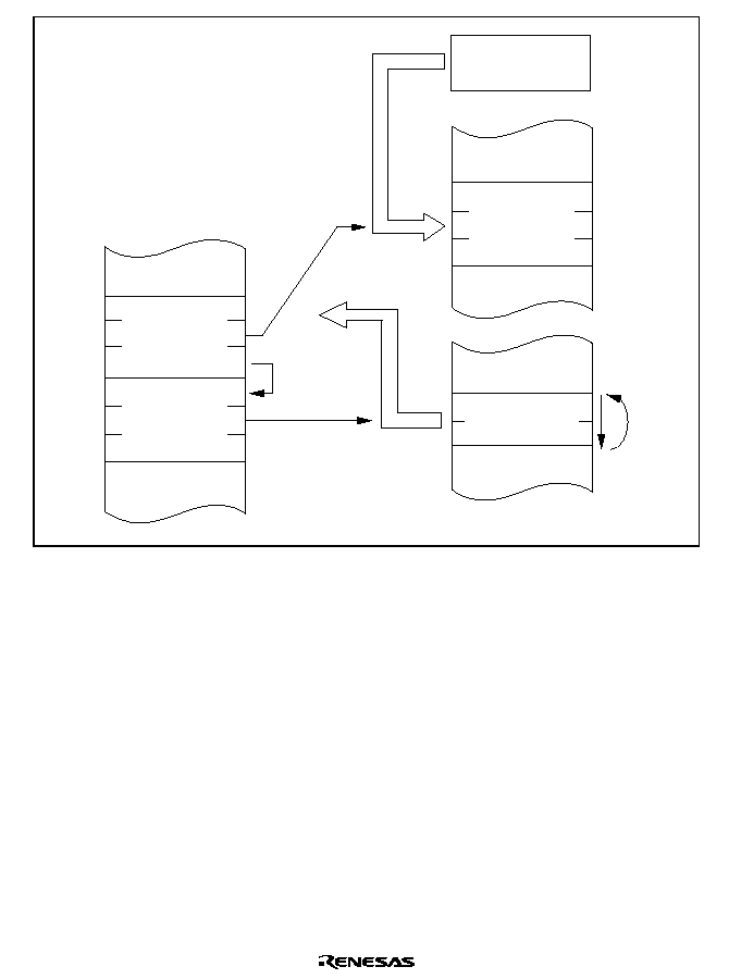
Rev. 2.0, 04/02, page 414 of 906
First data
transfer register
information
Second data
transfer register
information
Chain transfer
(counter = 0)
Upper 8 bits
of DAR
Input buffer
Input circuit
Figure 9.12 Chain Transfer when Counter = 0
9.7.4
Software Activation
An example is shown in which the DTC is used to transfer a block of 128 bytes of data by means
of software activation. The transfer source address is H'1000 and the destination address is
H'2000. The vector number is H'60, so the vector address is H'04C0.
1. Set MRA to incrementing source address (SM1 = 1, SM0 = 0), incrementing destination
address (DM1 = 1, DM0 = 0), block transfer mode (MD1 = 1, MD0 = 0), and byte size (Sz =
0). The DTS bit can have any value. Set MRB for one block transfer by one interrupt (CHNE =
0). Set the transfer source address (H'1000) in SAR, the destination address (H'2000) in DAR,
and 128 (H'8080) in CRA. Set 1 (H'0001) in CRB.
2. Set the start address of the register information at the DTC vector address (H'04C0).
3. Check that the SWDTE bit in DTVECR is 0. Check that there is currently no transfer activated
by software.
4. Write 1 to the SWDTE bit and the vector number (H'60) to DTVECR. The write data is H'E0.

Rev. 2.0, 04/02, page 415 of 906
5. Read DTVECR again and check that it is set to the vector number (H'60). If it is not, this
indicates that the write failed. This is presumably because an interrupt occurred between steps
3 and 4 and led to a different software activation. To activate this transfer, go back to step 3.
6. If the write was successful, the DTC is activated and a block of 128 bytes of data is transferred.
7. After the transfer, an SWDTEND interrupt occurs. The interrupt handling routine should clear
the SWDTE bit to 0 and perform other wrap-up processing.
9.8
Usage Notes
9.8.1
Module Stop Mode Setting
DTC operation can be disabled or enabled using the module stop control register. The initial
setting is for DTC operation to be enabled. Register access is disabled by setting module stop
mode. Module stop mode cannot be set while the DTC is activated. For details, refer to section 22,
Power-Down Modes.
9.8.2
On-Chip RAM
The MRA, MRB, SAR, DAR, CRA, and CRB registers are all located in on-chip RAM. When the
DTC is used, the RAME bit in SYSCR must not be cleared to 0.
9.8.3
DTCE Bit Setting
For DTCE bit setting, use bit manipulation instructions such as BSET and BCLR. If all interrupts
are disabled, multiple activation sources can be set at one time (only at the initial setting) by
writing data after executing a dummy read on the relevant register.
∑
DMAC Transfer End Interrupt
When DTC transfer is activated by a DMAC transfer end interrupt, regardless of the transfer
counter and DISEL bit, the DMAC's DTE bit is not subject to DTC control, and the write data
has priority. Consequently, an interrupt request may not be sent to the CPU when the DTC
transfer counter reaches 0.
∑
Chain Transfer
When chain transfer is used, clearing of the activation source or DTCER is performed when
the last of the chain of data transfers is executed. SCI and high-speed A/D converter
interrupt/activation sources, on the other hand, are cleared when the DTC reads or writes to the
prescribed register.
Therefore, when the DTC is activated by an interrupt or activation source, if a read/write of the
relevant register is not included in the last chained data transfer, the interrupt or activation
source will be retained.

Rev. 2.0, 04/02, page 416 of 906

Rev. 2.0, 04/02, page 417 of 906
Section 10 I/O Ports
Table 10.1 summarizes the port functions. The pins of each port also have other functions such as
input/output or external interrupt input pins of on-chip peripheral modules. Each I/O port includes
a data direction register (DDR) that controls input/output, a data register (DR) that stores output
data, and a port register (PORT) used to read the pin states. The input-only ports do not have a DR
or DDR register.
Ports A to E have a built-in pull-up MOS function and a input pull-up MOS control register (PCR)
to control the on/off state of input pull-up MOS.
Ports 3 and A include an open-drain control register (ODR) that controls the on/off state of the
output buffer PMOS.
Ports 1 to 3, 5 (P50 to P53), and 6 to 8 can drive a single TTL load and 30 pF capacitive load.
Ports A to H can drive a single TTL load and 50 pF capacitive load.
All the I/O ports can drive a Darlington transistor when outputting data.
Ports 1 and 2 are Schmitt-triggered inputs. Ports 5,6, F (PF1, PF2), and H (PH2, PH3) are Schmitt-
triggered inputs when used as the IRQ input.

Rev. 2.0, 04/02, page 418 of 906
Table 10.1
Port Functions
Modes 3
*
, 7
Port
Description
Modes 1
and 5
Modes 2
and 6
Mode 4
EXPE = 1
EXPE = 0
Input/
Output
Type
P17/PO15/TIOCB2/TCLKD/
('5$.
P17/PO15/TIOCB2/
TCLKD/
('5$.
P17/PO15/TIOCB2/
TCLKD
Schmitt-
triggered
input
P16/PO14/TIOCA2/
('5$.
P16/PO14/TIOCA2/
('5$.
P16/PO14/TIOCA2
Port
1
General I/O port
also functioning
as PPG outputs,
TPU I/Os, and
EXDMAC outputs
P15/PO13/TIOCB1/TCLKC
P14/PO12/TIOCA1
P13/PO11/TIOCD0/TCLKB
P12/PO10/TIOCC0/TCLKA
P11/PO9/TIOCB0
P10/PO8/TIOCA0
P27/PO7/TIOCB5/
('5$.
/
(
,54
)
P27/PO7/TIOCB5/
('5$.
/(
,54
)
P27/PO7/TIOCB5/
(
,54
)
Schmitt-
triggered
input
P26/PO6/TIOCA5/
('5$.
/
(
,54
)
P26/PO6/TIOCA5/
('5$.
/(
,54
)
P26/PO6/TIOCA5/
(
,54
)
Port
2
General I/O port
also functioning
as PPG outputs,
TPU I/Os,
interrupt inputs,
and EXDMAC
outputs
P25/PO5/TIOCB4/(
,54
)
P24/PO4/TIOCA4/(
,54
)
P23/PO3/TIOCD3/(
,54
)
P22/PO2/TIOCC3/(
,54
)
P21/PO1/TIOCB3/(
,54
)
P20/PO0/TIOCA3/(
,54
)
P35/SCK1/(
2(
)/CKE
*
P35/SCK1/(
2(
)/
CKE
*
P35/SCK1
Port
3
General I/O port
also functioning
as SCI I/Os
P34/SCK0
P33/RxD1
P32/RxD0/IrRxD
P31/TxD1
P30/TxD0/IrTxD
Open-
drain
output
capability

Rev. 2.0, 04/02, page 419 of 906
Modes 3
*
, 7
Port
Description
Modes 1
and 5
Modes 2
and 6
Mode 4
EXPE = 1
EXPE = 0
Input/
Output
Type
Port
4
General I/O port
also functioning
as A/D converter
analog inputs and
D/A converter
analog outputs
P47/AN7/DA1
P46/AN6/DA0
P45/AN5
P44/AN4
P43/AN3
P42/AN2
P41/AN1
P40/AN0
Port
5
General I/O port
also functioning
as interrupt
inputs, A/D
converter analog
inputs, and D/A
converter analog
outputs
P57/AN15/DA3/
,54
P56/AN14/DA2/
,54
P55/AN13/
,54
P54/AN12/
,54
Schmitt-
triggered
input
when
used as
input
General I/O port
also functioning
as interrupt
inputs, A/D
converter analog
inputs, and SCI
I/Os
P53/
$'75*
/
,54
P52/SCK2/
,54
P51/RxD2/
,54
P50/TxD2/
,54
Port
6
General I/O port
also functioning
as interrupt
inputs, TMR I/Os,
and DMAC I/Os
P65/TMO1/
'$&.
/
,54
P64/TMO0/
'$&.
/
,54
P63/TMCI1/
7(1'
/
,54
P62/TMCI0/
7(1'
/
,54
P61/TMRI1/
'5(4
/
,54
P60/TMRI0/
'5(4
/
,54
Schmitt-
triggered
input
when
used as
input
Port
7
General I/O port
also functioning
as DMAC I/Os
and EXDMAC
I/Os
P75/
('$&.
/(
'$&.
)
P74/
('$&.
/(
'$&.
)
P73/
(7(1'
/(
7(1'
)
P72/
(7(1'
/(
7(1'
)
P71/
('5(4
/(
'5(4
)
P70/
('5(4
/(
'5(4
)
P75/
('$&.
/
(
'$&.
)
P74/
('$&.
/
(
'$&.
)
P73/
(7(1'
/
(
7(1'
)
P72/
(7(1'
/
(
7(1'
)
P71/
('5(4
/
(
'5(4
)
P70/
('5(4
/
(
'5(4
)
P75/(
'$&.
)
P74/(
'$&.
)
P73/(
7(1'
)
P72/(
7(1'
)
P71/(
'5(4
)
P70/(
'5(4
)

Rev. 2.0, 04/02, page 420 of 906
Modes 3
*
, 7
Port
Description
Modes 1
and 5
Modes 2
and 6
Mode 4
EXPE = 1
EXPE = 0
Input/
Output
Type
Port
8
General I/O port
also functioning
as EXDMAC I/Os
and interrupt
inputs
P85/
('$&.
/
,54
P84/
('$&.
/
,54
P83/
(7(1'
/
,54
P82/
(7(1'
/
,54
P81/
('5(4
/
,54
P80/
('5(4
/
,54
P85/
('$&.
/
,54
P84/
('$&.
/
,54
P83/
(7(1'
/
,54
P82/
(7(1'
/
,54
P81/
('5(4
/
,54
P80/
('5(4
/
,54
P85/
,54
P84/
,54
P83/
,54
P82/
,54
P81/
,54
P80/
,54
Port
A
General I/O port
also functioning
as address
outputs
PA7/A23
PA6/A22
PA5/A21
A20
A19
A18
A17
A16
PA7/A23
PA6/A22
PA5/A21
PA4/A20
PA3/A19
PA2/A18
PA1/A17
PA0/A16
PA7/A23
PA6/A22
PA5/A21
PA4/A20
PA3/A19
PA2/A18
PA1/A17
PA0/A16
PA7
PA6
PA5
PA4
PA3
PA2
PA1
PA0
Built-in
input
pull-up
MOS
Open-
drain
output
capability
Port
B
General I/O port
also functioning
as address
outputs
A15
A14
A13
A12
A11
A10
A9
A8
PB7/A15
PB6/A14
PB5/A13
PB4/A12
PB3/A11
PB2/A10
PB1/A9
PB0/A8
PB7/A15
PB6/A14
PB5/A13
PB4/A12
PB3/A11
PB2/A10
PB1/A9
PB0/A8
PB7
PB6
PB5
PB4
PB3
PB2
PB1
PB0
Built-in
input
pull-up
MOS
Port
C
General I/O port
also functioning
as address
outputs
A7
A6
A5
A4
A3
A2
A1
A0
PC7/A7
PC6/A6
PC5/A5
PC4/A4
PC3/A3
PC2/A2
PC1/A1
PC0/A0
PC7/A7
PC6/A6
PC5/A5
PC4/A4
PC3/A3
PC2/A2
PC1/A1
PC0/A0
PC7
PC6
PC5
PC4
PC3
PC2
PC1
PC0
Built-in
input
pull-up
MOS

Rev. 2.0, 04/02, page 421 of 906
Modes 3
*
, 7
Port
Description
Modes 1
and 5
Modes 2
and 6
Mode 4
EXPE = 1
EXPE = 0
Input/
Output
Type
Port
D
General I/O port
also functioning
as data I/Os
D15
D14
D13
D12
D11
D10
D9
D8
D15
D14
D13
D12
D11
D10
D9
D8
PD7
PD6
PD5
PD4
PD3
PD2
PD1
PD0
Built-in
input
pull-up
MOS
Port
E
General I/O port
also functioning
as data I/Os
D7
D6
D5
D4
D3
D2
D1
D0
PE7/D7
PE6/D6
PE5/D5
PE4/D4
PE3/D3
PE2/D2
PE1/D1
PE0/D0
PE7/D7
PE6/D6
PE5/D5
PE4/D4
PE3/D3
PE2/D2
PE1/D1
PE0/D0
PE7/D7
PE6/D6
PE5/D5
PE4/D4
PE3/D3
PE2/D2
PE1/D1
PE0/D0
PE7
PE6
PE5
PE4
PE3
PE2
PE1
PE0
Built-in
input
pull-up
MOS
PF7/
PF6/
$6
5'
+:5
PF3/
/:5
PF7/
PF6/
$6
5'
+:5
PF3/
/:5
PF7/
PF6
PF5
PF4
PF3
PF2/
/&$6
/DQML
*
/
,54
PF2/
/&$6
/DQML
*
/
,54
PF2/
,54
PF1/
8&$6
/DQMU
*
/
,54
PF1/
8&$6
/DQMU
*
/
,54
PF1/
,54
Port
F
General I/O port
also functioning
as interrupt inputs
and bus control
I/Os
PF0/
:$,7
PF0/
:$,7
PF0
Only PF1
and PF2
are
Schmitt-
triggered
inputs
when
used as
the IRQ
input
Port
G
General I/O port
also functioning
as bus control
I/Os
PG6/
%5(4
PG5/
%$&.
PG4/
%5(42
PG3/
&6
/
5$6
/
&$6*
PG2/
&6
/
5$6
/
5$6*
PG1/
&6
PG0/
&6
PG6/
%5(4
PG5/
%$&.
PG4/
%5(42
PG3/
&6
/
5$6
/
&$6*
PG2/
&6
/
5$6
/
5$6*
PG1/
&6
PG0/
&6
PG6
PG5
PG4
PG3
PG2
PG1
PG0

Rev. 2.0, 04/02, page 422 of 906
Modes 3
*
, 7
Port
Description
Modes 1
and 5
Modes 2
and 6
Mode 4
EXPE = 1
EXPE = 0
Input/
Output
Type
PH3/
&6
/
2(
/CKE
*
/(
,54
)
PH3/
&6
/
2(
/CKE
*
/
(
,54
)
PH3/(
,54
)
PH2/
&6
/(
,54
)
PH2/
&6
/(
,54
)
PH2/(
,54
)
PH1/
&6
/
5$6
/SDRAM
*
PH1/
&6
/
5$6
/
SDRAM
*
PH1/SDRAM
*
Port
H
General I/O port
also functioning
as interrupt inputs
and bus control
I/Os
PH0/
&6
/
5$6
/
:(*
PH0/
&6
/
5$6
/
:(*
PH0
Only PH2
and PH3
are
Schmitt-
triggered
inputs
when
used as
the IRQ
input
Note: Only in H8S/2678R Series.
10.1
Port 1
Port 1 is an 8-bit I/O port that also has other functions. The port 1 has the following registers.
∑
Port 1 data direction register (P1DDR)
∑
Port 1 data register (P1DR)
∑
Port 1 register (PORT1)
10.1.1
Port 1 Data Direction Register (P1DDR)
The individual bits of P1DDR specify input or output for the pins of port 1.
P1DDR cannot be read; if it is, an undefined value will be read.
Bit
Bit Name
Initial Value
R/W
Description
7
P17DDR
0
W
6
P16DDR
0
W
5
P15DDR
0
W
4
P14DDR
0
W
3
P13DDR
0
W
2
P12DDR
0
W
1
P11DDR
0
W
0
P10DDR
0
W
When a pin function is specified to a general purpose
I/O, setting this bit to 1 makes the corresponding port
1 pin an output pin, while clearing this bit to 0 makes
the pin an input pin.

Rev. 2.0, 04/02, page 423 of 906
10.1.2
Port 1 Data Register (P1DR)
P1DR stores output data for the port 1 pins.
Bit
Bit Name
Initial Value
R/W
Description
7
P17DR
0
R/W
6
P16DR
0
R/W
5
P15DR
0
R/W
4
P14DR
0
R/W
3
P13DR
0
R/W
2
P12DR
0
R/W
1
P11DR
0
R/W
0
P10DR
0
R/W
Output data for a pin is stored when the pin function
is specified to a general purpose I/O.
10.1.3
Port 1 Register (PORT1)
PORT1 shows the pin states.
PORT1 cannot be modified.
Bit
Bit Name
Initial Value
R/W
Description
7
P17
Undefined
*
R
6
P16
Undefined
*
R
5
P15
Undefined
*
R
4
P14
Undefined
*
R
3
P13
Undefined
*
R
2
P12
Undefined
*
R
1
P11
Undefined
*
R
0
P10
Undefined
*
R
If a port 1 read is performed while P1DDR bits are
set to 1, the P1DR values are read. If a port 1 read is
performed while P1DDR bits are cleared to 0, the pin
states are read.
Note: Determined by the states of pins P17 to P10.
Rev. 2.0, 04/02, page 424 of 906
10.1.4
Pin Functions
Port 1 pins also function as PPG outputs, TPU I/Os, and EXDMAC outputs. The correspondence
between the register specification and the pin functions is shown below.
∑
P17/PO15/TIOCB2/TCLKD/
('5$.
The pin function is switched as shown below according to the combination of the TPU channel
2 settings (by bits MD3 to MD0 in TMDR2, bits IOB3 to IOB0 in TIOR2, and bits CCLR1
and CCLR0 in TCR2), bits TPSC2 to TPSC0 in TCR0 and TCR5, bit NDER15 in NDERH, bit
EDRAKE in EDMDR3, and bit P17DDR.
Modes 1, 2, 3*
3
(EXPE = 1), 4, 5, 6, 7 (EXPE = 1)
EDRAKE
0
1
TPU channel 2
settings
(1) in table
below
(2) in table below
--
P17DDR
--
0
1
1
--
NDER15
--
--
0
1
--
P17
input
P17
output
PO15
output
('5$.
output
TIOCB2
output
TIOCB2 input
*
1
Pin function
TCLKD input
*
2
Modes 3*
3
(EXPE = 0), 7 (EXPE = 0)
EDRAKE
--
TPU channel 2
settings
(1) in table
below
(2) in table below
P17DDR
--
0
1
1
NDER15
--
--
0
1
P17 input
P17 output
PO15 output
TIOCB2 output
TIOCB2 input
*
1
Pin function
TCLKD input
*
2
Notes: 1. TIOCB2 input when MD3 to MD0 = B'0000 or B'01xx and IOB3 = 1.
2. TCLKD input when the setting for either TCR0 or TCR5 is TPSC2 to TPSC0 = B'111.
TCLKD input when channels 2 and 4 are set to phase counting mode.
3. Only in H8S/2678R Series.
Rev. 2.0, 04/02, page 425 of 906
TPU channel 2
settings
(2)
(1)
(2)
(2)
(1)
(2)
MD3 to MD0
B'0000, B'01xx
B'0010
B'0011
IOB3 to IOB0
B'0000
B'0100
B'1xxx
B'0001 to B'0011
B'0101 to B'0111
B'xx00
B'xx00
Other than B'xx00
CCLR1, CCLR0
--
--
--
--
Other
than
B'10
B'10
Output function
--
Output compare
output
--
--
PWM
mode 2
output
--
x: Don't care
∑
P16/PO14/TIOCA2/
('5$.
The pin function is switched as shown below according to the combination of the TPU channel
2 settings (by bits MD3 to MD0 in TMDR2, bits IOB3 to IOB0 in TIOR2, and bits CCLR1
and CCLR0 in TCR2), bit NDER14 in NDERH, bit EDRAKE in EDMDR2 and bit P16DDR.
Modes 1, 2, 3*
3
(EXPE = 1), 4, 5, 6, 7 (EXPE = 1)
EDRAKE
0
1
TPU channel 2
settings
(1) in table
below
(2) in table below
--
P16DDR
--
0
1
1
--
NDER14
--
--
0
1
--
TIOCA2
output
P16
input
P16
output
PO14
output
('5$.
output
Pin function
TIOCA input
*
1
Modes 3*
3
(EXPE = 0), 7 (EXPE = 0)
EDRAKE
--
TPU channel 2
settings
(1) in table
below
(2) in table below
P16DDR
--
0
1
1
NDER14
--
--
0
1
P16 input
P16 output
PO14 output
Pin function
TIOCA2 output
TIOCA2 input
*
1
Note:
1. TIOCA2 input when MD3 to MD0 = B'0000 or B'01xx and IOA3 = 1.
Rev. 2.0, 04/02, page 426 of 906
TPU channel 2
settings
(2)
(1)
(2)
(1)
(1)
(2)
MD3 to MD0
B'0000, B'01xx
B'001x
B'0010
B'0011
IOA3 to IOA0
B'0000
B'0100
B'1xxx
B'0001 to B'0011
B'0101 to B'0111
B'xx00
Other than B'xx00
CCLR1, CCLR0
--
--
--
--
Other
than
B'10
B'10
Output function
--
Output compare
output
--
PWM
*
2
mode 1
output
PWM
mode 2
output
--
x: Don't care
Notes: 2. TIOCB2 output disabled.
3. Only in H8S/2678R Series.
∑
P15/PO13/TIOCB1/TCLKC
The pin function is switched as shown below according to the combination of the TPU channel
1 settings (by bits MD3 to MD0 in TMDR1, bits IOB3 to IOB0 in TIOR1, and bits CCLR1
and CCLR0 in TCR1), bits TPSC2 to TPSC0 in TCR0, TCR2, TCR4, and TCR5, bit NDER13
in NDERH, and bit P15DDR.
TPU channel 1
settings
(1) in table
below
(2) in table below
P15DDR
--
0
1
1
NDER13
--
--
0
1
P15 input
P15 output
PO13 output
TIOCB1 output
TIOCB1 input
*
1
Pin function
TCLKC input
*
2
Notes: 1. TIOCB1 input when MD3 to MD0 = B'0000 or B'01XX and IOB3 to IOB0 = B'10xx.
2. TCLKC input when the setting for either TCR0 or TCR2 is TPSC2 to TPSC0 = B'110, or
when the setting for either TCR4 or TCR5 is TPSC2 to TPSC0 = B'101.
TCLKC input when phase counting mode is set for channels 2 and 4.
Rev. 2.0, 04/02, page 427 of 906
TPU channel 1
settings
(2)
(1)
(2)
(2)
(1)
(2)
MD3 to MD0
B'0000, B'01xx
B'0010
B'0011
IOB3 to IOB0
B'0000
B'0100
B'1xxx
B'0001 to B'0011
B'0101 to B'0111
B'xx00
B'xx00
Other than B'xx00
CCLR1, CCLR0
--
--
--
--
Other
than
B'10
B'10
Output function
--
Output compare
output
--
--
PWM
mode 2
output
--
x: Don't care
∑
P14/PO12/TIOCA1
The pin function is switched as shown below according to the combination of the TPU channel
1 settings (by bits MD3 to MD0 in TMDR1, bits IOA3 to IOA0 in TIOR1, and bits CCLR1
and CCLR0 in TCR1), bit NDER12 in NDERH, and bit P14DDR.
TPU channel 1
settings
(1) in table
below
(2) in table below
P14DDR
--
0
1
1
NDER12
--
--
0
1
P14 input
P14 output
PO12 output
Pin function
TIOCA1 output
TIOCA1 input
*
1
Note: 1. TIOCA1 input when MD3 to MD0 = B'0000 or B'01xx and IOA3 to IOA0 = B'10xx.
TPU channel 1
settings
(2)
(1)
(2)
(1)
(1)
(2)
MD3 to MD0
B'0000, B'01xx
B'001x
B'0010
B'0011
IOA3 to IOA0
B'0000
B'0100
B'1xxx
B'0001 to B'0011
B'0101 to B'0111
B'xx00
Other
than
B'xx00
Other than B'xx00
CCLR1, CCLR0
--
--
--
--
Other
than
B'01
B'01
Output function
--
Output compare
output
--
PWM
*
2
mode 1
output
PWM
mode 2
output
--
x: Don't care
Note:
2. TIOCB1 output disabled.
Rev. 2.0, 04/02, page 428 of 906
∑
P13/PO11/TIOCD0/TCLKB
The pin function is switched as shown below according to the combination of the TPU channel
0 settings (by bits MD3 to MD0 in TMDR0, bits IOD3 to IOD0 in TIOR0L, and bits CCLR2
to CCLR0 in TCR0), bits TPSC2 to TPSC0 in TCR0 to TCR2, bit NDER11 in NDERH, and
bit P13DDR.
TPU channel 0
settings
(1) in table
below
(2) in table below
P13DDR
--
0
1
1
NDER11
--
--
0
1
P13 input
P13 output
PO11 output
TIOCD0 output
TIOCD0 input
*
1
Pin function
TCLKB input
*
2
Notes: 1. TIOCD0 input when MD3 to MD0 = B'0000 or B'01xx and IOD3 to IOD0 = B'10xx.
2. TCLKB input when the setting for any of TCR0 to TCR2 is TPSC2 to TPSC0 = B'101.
TCLKB input when phase counting mode is set for channels 1 and 5.
TPU channel 0
settings
(2)
(1)
(2)
(2)
(1)
(2)
MD3 to MD0
B'0000
B'0010
B'0011
IOD3 to IOD0
B'0000
B'0100
B'1xxx
B'0001 to B'0011
B'0101 to B'0111
--
B'xx00
Other than B'xx00
CCLR2, CCLR0
--
--
--
--
Other
than
B'110
B'110
Output function
--
Output compare
output
--
--
PWM
mode 2
output
--
x: Don't care
Rev. 2.0, 04/02, page 429 of 906
∑
P12/PO10/TIOCC0/TCLKA
The pin function is switched as shown below according to the combination of the TPU channel
0 settings (by bits MD3 to MD0 in TMDR0, bits IOC3 to IOC0 in TIOR0L, and bits CCLR2
to CCLR0 in TCR0), bits TPSC2 to TPSC0 in TCR0 to TCR5, bit NDER10 in NDERH, and
bit P12DDR.
TPU channel 0
settings
(1) in table
below
(2) in table below
P12DDR
--
0
1
1
NDER10
--
--
0
1
P12 input
P12 output
PO10 output
TIOCC0 output
TIOCC0 input
*
1
Pin function
TCLKA input
*
2
Notes: 1. TIOCC0 input when MD3 to MD0 = B'0000 and IOC3 to IOC0 = B'10xx.
2. TCLKA input when the setting for any of TCR0 to TCR5 is TPSC2 to TPSC0 = B'100.
TCLKA input when phase counting mode is set for channels 1 and 5.
TPU channel 0
settings
(2)
(1)
(2)
(1)
(1)
(2)
MD3 to MD0
B'0000
B'001x
B'0010
B'0011
IOC3 to IOC0
B'0000
B'0100
B'1xxx
B'0001 to B'0011
B'0101 to B'0111
B'xx00
Other
than
B'xx00
Other than B'xx00
CCLR2, CCLR0
--
--
--
--
Other
than
B'101
B'101
Output function
--
Output compare
output
--
PWM
*
3
mode 1
output
PWM
mode 2
output
--
x: Don't care
Note:
3. TIOCD0 output disabled.
Output disabled and settings (2) effective when BFA = 1 or BFB = 1 in TMDR0.
Rev. 2.0, 04/02, page 430 of 906
∑
P11/PO9/TIOCB0
The pin function is switched as shown below according to the combination of the TPU channel
0 settings (by bits MD3 to MD0 in TMDR0 and bits IOB3 to IOB0 in TIOR0H), bit NDER9 in
NDERH, and bit P11DDR.
TPU channel 0
settings
(1) in table
below
(2) in table below
P11DDR
--
0
1
1
NDER9
--
--
0
1
P11 input
P11 output
PO9 output
Pin function
TIOCB0 output
TIOCB0 input
*
1
Note:
1. TIOCB0 input when MD3 to MD0 = B'0000 and IOB3 to IOB0 = B'10xx.
TPU channel 0
settings
(2)
(1)
(2)
(2)
(1)
(2)
MD3 to MD0
B'0000
B'0010
B'0011
IOB3 to IOB0
B'0000
B'0100
B'1xxx
B'0001 to B'0011
B'0101 to B'0111
--
B'xx00
Other than B'xx00
CCLR2, CCLR0
--
--
--
--
Other
than
B'010
B'010
Output function
--
Output compare
output
--
--
PWM
mode 2
output
--
x: Don't care
∑
P10/PO8/TIOCA0
The pin function is switched as shown below according to the combination of the TPU channel
0 settings (by bits MD3 to MD0 in TMDR0, bits IOA3 to IOA0 in TIOR0H, and bits CCLR2
to CCLR0 in TCR0), bit NDER8 in NDERH, and bit P10DDR.
TPU channel 0
settings
(1) in table
below
(2) in table below
P10DDR
--
0
1
1
NDER8
--
--
0
1
P10 input
P10 output
PO8 output
Pin function
TIOCA0 output
TIOCA0 input
*
1
Note: 1. TIOCA0 input when MD3 to MD0 = B'0000 and IOA3 to IOA0 = B'10xx.

Rev. 2.0, 04/02, page 431 of 906
TPU channel 0
settings
(2)
(1)
(2)
(1)
(1)
(2)
MD3 to MD0
B'0000
B'001x
B'0010
B'0011
IOA3 to IOA0
B'0000
B'0100
B'1xxx
B'0001 to B'0011
B'0101 to B'0111
B'xx00
Other
than
B'xx00
Other than B'xx00
CCLR2, CCLR0
--
--
--
--
Other
than
B'001
B'001
Output function
--
Output compare
output
--
PWM
*
2
mode 1
output
PWM
mode 2
output
--
x: Don't care
Note: 2. TIOCB0 output disabled.
10.2
Port 2
Port 2 is an 8-bit I/O port that also has other functions. The port 2 has the following registers.
∑
Port 2 data direction register (P2DDR)
∑
Port 2 data register (P2DR)
∑
Port 2 register (PORT2)
10.2.1
Port 2 Data Direction Register (P2DDR)
The individual bits of P2DDR specify input or output for the pins of port 2.
P2DDR cannot be read; if it is, an undefined value will be read.
Bit
Bit Name
Initial Value
R/W
Description
7
P27DDR
0
W
6
P26DDR
0
W
5
P25DDR
0
W
4
P24DDR
0
W
3
P23DDR
0
W
2
P22DDR
0
W
1
P21DDR
0
W
0
P20DDR
0
W
When a pin function is specified to a general purpose
I/O, setting this bit to 1 makes the corresponding port
1 pin an output pin, while clearing this bit to 0 makes
the pin an input pin.

Rev. 2.0, 04/02, page 432 of 906
10.2.2
Port 2 Data Register (P2DR)
P2DR stores output data for the port 2 pins.
Bit
Bit Name
Initial Value
R/W
Description
7
P27DR
0
R/W
6
P26DR
0
R/W
5
P25DR
0
R/W
4
P24DR
0
R/W
3
P23DR
0
R/W
2
P22DR
0
R/W
1
P21DR
0
R/W
0
P20DR
0
R/W
Output data for a pin is stored when the pin function
is specified to a general purpose I/O.
10.2.3
Port 2 Register (PORT2)
PORT2 shows the pin states.
PORT2 cannot be modified.
Bit
Bit Name
Initial Value
R/W
Description
7
P27
Undefined
*
R
6
P26
Undefined
*
R
5
P25
Undefined
*
R
4
P24
Undefined
*
R
3
P23
Undefined
*
R
2
P22
Undefined
*
R
1
P21
Undefined
*
R
0
P20
Undefined
*
R
If a port 2 read is performed while P2DDR bits are
set to 1, the P2DR values are read. If a port 2 read is
performed while P2DDR bits are cleared to 0, the pin
states are read.
Note: Determined by the states of pins P27 to P20.
Rev. 2.0, 04/02, page 433 of 906
10.2.4
Pin Functions
Port 2 pins also function as PPG outputs, TPU I/Os, interrupt inputs, and EXDMAC outputs. The
correspondence between the register specification and the pin functions is shown below.
∑
P27/PO7/TIOCB5/
,54/('5$.
The pin function is switched as shown below according to the combination of the TPU channel
5 settings (by bits MD3 to MD0 in TMDR5, bits IOB3 to IOB0 in TIOR5, and bits CCLR1
and CCLR0 in TCR5), bit NDER7 in NDERL, bit EDRAKE in EDMDR1, bit P27DDR, and
bit ITS15 in ITSR.
Modes 1, 2, 3*
3
(EXPE = 1), 4, 5, 6, 7 (EXPE = 1)
EDRAKE
0
1
TPU channel 5
settings
(1) in table
below
(2) in table below
--
P27DDR
--
0
1
1
--
NDER7
--
--
0
1
--
P27
input
P27
output
PO7
output
('5$.
output
TIOCB5
output
TIOCB5 input
*
1
Pin function
,54
interrupt input
*
2
Mode, 3*
3
(EXPE = 0), 7 (EXPE = 0)
EDRAKE
--
TPU channel 5
settings
(1) in table
below
(2) in table below
P27DDR
--
0
1
1
NDER7
--
--
0
1
P27 input
P27 output
PO7 output
TIOCB5 output
TIOCB5 input
*
1
Pin function
,54
interrupt input
*
2
Notes: 1. TIOCB5 input when MD3 to MD0 = B'0000 or B'01xx and IOB3 = 1.
2.
,54
input when ITS15 = 1.
3. Only in H8S/2678R Series.
Rev. 2.0, 04/02, page 434 of 906
TPU channel 5
settings
(2)
(1)
(2)
(2)
(1)
(2)
MD3 to MD0
B'0000, B'01xx
B'0010
B'0011
IOB3 to IOB0
B'0000
B'0100
B'1xxx
B'0001 to B'0011
B'0101 to B'0111
B'xx00
Other than B'xx00
CCLR1, CCLR0
--
--
--
--
Other
than
B'10
B'10
Output function
--
Output compare
output
--
--
PWM
mode 2
output
--
x: Don't care
∑
P26/PO6/TIOCA5/
,54/('5$.
The pin function is switched as shown below according to the combination of the TPU channel
5 settings (by bits MD3 to MD0 in TMDR5, bits IOA3 to IOA0 in TIOR5, and bits CCLR1
and CCLR0 in TCR5), bit NDER6 in NDERL, bit EDRAKE in EDMDR0, bit P26DDR, and
bit ITS14 in ITSR.
Modes 1, 2, 3*
4
(EXPE = 1), 4, 5, 6, 7 (EXPE = 1)
EDRAKE
0
1
TPU channel 5
settings
(1) in table
below
(2) in table below
--
P26DDR
--
0
1
1
--
NDER6
--
--
0
1
--
P26
input
P26
output
PO6
output
('5$.
output
TIOCA5
output
TIOCA input
*
1
Pin function
,54
interrupt input
*
2
Rev. 2.0, 04/02, page 435 of 906
Modes 3*
4
(EXPE = 0), 7 (EXPE = 0)
EDRAKE
--
TPU channel 5
settings
(1) in table
below
(2) in table below
P26DDR
--
0
1
1
NDER6
--
--
0
1
P26 input
P26 output
PO6 output
TIOCA5 output
TIOCA5 input
*
1
Pin function
,54
interrupt input
*
2
Notes: 1. TIOCA5 input when MD3 to MD0 = B'0000 or B'01xx and IOA3 = 1.
2.
,54
input when ITS14 = 1.
TPU channel 5
settings
(2)
(1)
(2)
(2)
(1)
(2)
MD3 to MD0
B'0000, B'01xx
B'001x
B'0010
B'0011
IOA3 to IOA0
B'0000
B'0100
B'1xxx
B'0001 to B'0011
B'0101 to B'0111
B'xx00
Other
than
B'xx00
Other than B'xx00
CCLR1, CCLR0
--
--
--
--
Other
than
B'01
B'01
Output function
--
Output compare
output
--
PWM
*
3
mode 1
output
PWM
mode 2
output
--
x: Don't care
Note:
3. TIOCB5 output disabled.
4. Only in H8S/2678R Series.
Rev. 2.0, 04/02, page 436 of 906
∑
P25/PO5/TIOCB4/
,54
The pin function is switched as shown below according to the combination of the TPU channel
4 settings (by bits MD3 to MD0 in TMDR4, bits IOB3 to IOB0 in TIOR4, and bits CCLR1
and CCLR0 in TCR4), bit NDER5 in NDERL, bit P25DDR, and bit ITS13 in ITSR.
TPU channel 4
settings
(1) in table
below
(2) in table below
P25DDR
--
0
1
1
NDER5
--
--
0
1
P25 input
P25 output
PO5 output
TIOCB4 output
TIOCB4 input
*
1
Pin function
,54
interrupt input
*
2
Notes: 1. TIOCB4 input when MD3 to MD0 = B'0000 or B'01xx and IOB3 to IOB0 = B'10xx.
2.
,54
input when ITS13 = 1.
TPU channel 5
settings
(2)
(1)
(2)
(2)
(1)
(2)
MD3 to MD0
B'0000, B'01xx
B'0010
B'0011
IOB3 to IOB0
B'0000
B'0100
B'1xxx
B'0001 to B'0011
B'0101 to B'0111
--
B'xx00
Other than B'xx00
CCLR1, CCLR0
--
--
--
--
Other
than
B'10
B'10
Output function
--
Output compare
output
--
--
PWM
mode 2
output
--
x: Don't care
Rev. 2.0, 04/02, page 437 of 906
∑
P24/PO4/TIOCA4/
,54
The pin function is switched as shown below according to the combination of the TPU channel
4 settings (by bits MD3 to MD0 in TMDR4 and bits IOA3 to IOA0 in TIOR4), bit NDER4 in
NDERL, bit P24DDR, and bit ITS12 in ITSR.
TPU channel 4
settings
(1) in table
below
(2) in table below
P24DDR
--
0
1
1
NDER4
--
--
0
1
P24 input
P24 output
PO4 output
TIOCA4 output
TIOCA4 input
*
1
Pin function
,54
interrupt input
*
2
Notes: 1. TIOCA4 input when MD3 to MD0 = B'0000 or B'01xx and IOA3 to IOA0 = B'10xx.
2.
,54
input when ITS12 = 1.
TPU channel 4
settings
(2)
(1)
(2)
(1)
(1)
(2)
MD3 to MD0
B'0000, B'01xx
B'001x
B'0010
B'0011
IOA3 to IOA0
B'0000
B'0100
B'1xxx
B'0001 to B'0011
B'0101 to B'0111
B'xx00
Other
than
B'xx00
Other than B'xx00
CCLR1, CCLR0
--
--
--
--
Other
than
B'01
B'01
Output function
--
Output compare
output
--
PWM
*
3
mode 1
output
PWM
mode 2
output
--
x: Don't care
Note:
3. TIOCB4 output disabled.

Rev. 2.0, 04/02, page 438 of 906
∑
P23/PO3/TIOCD3/
,54
The pin function is switched as shown below according to the combination of the TPU channel
3 settings (by bits MD3 to MD0 in TMDR3, bits IOD3 to IOD0 in TIOR3L, and bits CCLR2
to CCLR0 in TCR3), bit NDER3 in NDERL, bit P23DDR, and bit ITS11 in ITSR.
TPU channel 3
settings
(1) in table
below
(2) in table below
P23DDR
--
0
1
1
NDER3
--
--
0
1
P23 input
P23 output
PO3 output
TIOCD3 output
TIOCD3 input
*
1
Pin function
,54
interrupt input
*
2
Notes: 1. TIOCD3 input when MD3 to MD0 = B'0000 and IOD3 to IOD0 = B'10xx.
2.
,54
input when ITS11 = 1.
TPU channel 3
settings
(2)
(1)
(2)
(2)
(1)
(2)
MD3 to MD0
B'0000
B'0010
B'0011
IOD3 to IOD0
B'0000
B'0100
B'1xxx
B'0001 to B'0011
B'0101 to B'0111
--
B'xx00
Other than B'xx00
CCLR2 to
CCLR0
--
--
--
--
Other
than
B'110
B'110
Output function
--
Output compare
output
--
--
PWM
mode 2
output
--
x: Don't care

Rev. 2.0, 04/02, page 439 of 906
∑
P22/PO2/TIOCC3/
,54
The pin function is switched as shown below according to the combination of the TPU channel
3 settings (by bits MD3 to MD0 in TMDR3, bits IOC3 to IOC0 in TIOR3L, and bits CCLR2
to CCLR0 in TCR3), bit NDER2 in NDERL, bit P22DDR, and bit ITS10 in ITSR.
TPU channel 3
settings
(1) in table
below
(2) in table below
P22DDR
--
0
1
1
NDER2
--
--
0
1
P22 input
P22 output
PO2 output
TIOCC3 output
TIOCC3 input
*
1
Pin function
,54
interrupt input
*
2
Notes: 1. TIOCC3 input when MD3 to MD0 = B'0000 and IOC3 to IOC0 = B'10xx.
2.
,54
input when ITS10 = 1.
TPU channel 3
settings
(2)
(1)
(2)
(1)
(1)
(2)
MD3 to MD0
B'0000
B'001x
B'0010
B'0011
IOC3 to IOC0
B'0000
B'0100
B'1xxx
B'0001 to B'0011
B'0101 to B'0111
B'xx00
Other
than
B'xx00
Other than B'xx00
CCLR2 to
CCLR0
--
--
--
--
Other
than
B'101
B'101
Output function
--
Output compare
output
--
PWM
*
3
mode 1
output
PWM
mode 2
output
--
x: Don't care
Note:
3. TIOCD3 output disabled.
Output disabled and settings (2) effective when BFA = 1 or BFB = 1 in TMDR3.

Rev. 2.0, 04/02, page 440 of 906
∑
P21/PO1/TIOCB3/
,54
The pin function is switched as shown below according to the combination of the TPU channel
3 settings (by bits MD3 to MD0 in TMDR3, bits IOB3 to IOB0 in TIOR3H, and bits CCLR2
to CCLR0 in TCR3), bit NDER1 in NDERL, bit P21DDR, and bit ITS9 in ITSR.
TPU channel 3
settings
(1) in table
below
(2) in table below
P21DDR
--
0
1
1
NDER1
--
--
0
1
P21 input
P21 output
PO1 output
TIOCB3 output
TIOCB3 input
*
1
Pin function
,54
interrupt input
*
2
Notes: 1. TIOCB3 input when MD3 to MD0 = B'0000 and IOB3 to IOB0 = B'10xx.
2.
,54
input when ITS9 = 1.
TPU channel 3
settings
(2)
(1)
(2)
(2)
(1)
(2)
MD3 to MD0
B'0000
B'0010
B'0011
IOB3 to IOB0
B'0000
B'0100
B'1xxx
B'0001 to B'0011
B'0101 to B'0111
--
B'xx00
Other than B'xx00
CCLR2 to
CCLR0
--
--
--
--
Other
than
B'010
B'010
Output function
--
Output compare
output
--
--
PWM
mode 2
output
--
x: Don't care
Rev. 2.0, 04/02, page 441 of 906
∑
P20/PO0/TIOCA3/
,54
The pin function is switched as shown below according to the combination of the TPU channel
3 settings (by bits MD3 to MD0 in TMDR3, bits IOA3 to IOA0 in TIOR3H, and bits CCLR2
to CCLR0 in TCR3), bit NDER0 in NDERL, bit P20DDR, and bit ITS8 in ITSR.
TPU channel 3
settings
(1) in table
below
(2) in table below
P20DDR
--
0
1
1
NDER0
--
--
0
1
P20 input
P20 output
PO0 output
TIOCA3 output
TIOCA3 input
*
1
Pin function
,54
interrupt input
*
2
Notes: 1. TIOCA3 input when MD3 to MD0 = B'0000 and IOA3 to IOA0 = B'10xx.
2.
,54
input when ITS8 = 1.
TPU channel 3
settings
(2)
(1)
(2)
(1)
(1)
(2)
MD3 to MD0
B'0000
B'001x
B'0010
B'0011
IOA3 to IOA0
B'0000
B'0100
B'1xxx
B'0001 to B'0011
B'0101 to B'0111
B'xx00
Other
than
B'xx00
Other than B'xx00
CCLR2 to
CCLR0
--
--
--
--
Other
than
B'001
B'001
Output function
--
Output compare
output
--
PWM
*
3
mode 1
output
PWM
mode 2
output
--
x: Don't care
Note:
3. TIOCB3 output disabled.
10.3
Port 3
Port 3 is a 6-bit I/O port that also has other functions. The port 3 has the following registers.
∑
Port 3 data direction register (P3DDR)
∑
Port 3 data register (P3DR)
∑
Port 3 register (PORT3)
∑
Port 3 open drain control register (P3ODR)
∑
Port function control register 2(PFCR2)

Rev. 2.0, 04/02, page 442 of 906
10.3.1
Port 3 Data Direction Register (P3DDR)
The individual bits of P3DDR specify input or output for the pins of port 3.
P3DDR cannot be read; if it is, an undefined value will be read.
Bit
Bit Name
Initial Value
R/W
Description
7
--
0
--
6
--
0
--
Reserved
These bits are always read as 0 and cannot be
modified.
5
P35DDR
0
W
4
P34DDR
0
W
3
P33DDR
0
W
2
P32DDR
0
W
1
P31DDR
0
W
0
P30DDR
0
W
When a pin function is specified to a general purpose
I/O, setting this bit to 1 makes the corresponding port
1 pin an output pin, while clearing this bit to 0 makes
the pin an input pin.
10.3.2
Port 3 Data Register (P3DR)
P3DR stores output data for the port 3 pins.
Bit
Bit Name
Initial Value
R/W
Description
7
--
0
--
6
--
0
--
Reserved
These bits are always read as 0 and cannot be
modified.
5
P35DR
0
R/W
4
P34DR
0
R/W
3
P33DR
0
R/W
2
P32DR
0
R/W
1
P31DR
0
R/W
0
P30DR
0
R/W
Output data for a pin is stored when the pin function
is specified to a general purpose I/O.

Rev. 2.0, 04/02, page 443 of 906
10.3.3
Port 3 Register (PORT3)
PORT3 shows the pin states.
PORT3 cannot be modified.
Bit
Bit Name
Initial Value
R/W
Description
7
--
0
--
6
--
0
--
Reserved
These bits are always read as 0 and cannot be
modified.
5
P35
Undefined
*
R
4
P34
Undefined
*
R
3
P33
Undefined
*
R
2
P32
Undefined
*
R
1
P31
Undefined
*
R
0
P30
Undefined
*
R
If a port 3 read is performed while P3DDR bits are
set to 1, the P3DR values are read. If a port 1 read is
performed while P3DDR bits are cleared to 0, the pin
states are read.
Note: Determined by the states of pins P35 to P30.
10.3.4
Port 3 Open Drain Control Register (P3ODR)
P3ODR controls the output status for each port 3 pin.
Bit
Bit Name
Initial Value
R/W
Description
7
--
0
--
6
--
0
--
Reserved
These bits are always read as 0 and cannot be
modified.
5
P35ODR
0
R/W
4
P34ODR
0
R/W
3
P33ODR
0
R/W
2
P32ODR
0
R/W
1
P31ODR
0
R/W
0
P30ODR
0
R/W
Setting a P3ODR bit to 1 makes the corresponding
port 3 pin an NMOS open-drain output pin, while
clearing the bit to 0 makes the pin a CMOS output
pin.

Rev. 2.0, 04/02, page 444 of 906
10.3.5
Port Function Control Register 2 (PFCR2)
P3ODR controls the I/O port.
Bit
Bit Name
Initial Value
R/W
Description
7
to
4
--
All 0
--
Reserved
These bits are always read as 0 and cannot be
modified.
3
ASOE
1
R/W
$6
Output Enable
Selects to enable or disable the AS output pin.
0: PF6 is designated as I/O port
1: PF6 is designated as
$6
output pin
2
LWROE
1
R/W
/:5
Output Enable
Selects to enable or disable the
/:5
output pin.
0: PF3 is designated as I/O port
1: PF3 is designated as
/:5
output pin
1
OES
1
R/W
2(
Output Select
Selects the
2(
output pin port when the OEE bit is
set to 1 in DRAMCR (enabling
2(
/CKE
*
output).
0: P35 is designated as
2(
output pin
1: PH3 is designated as
2(
/CKE
*
output pin
0
DMACS
0
R/W
DMAC Control Pin Select
Selects the DMAC control I/O port.
0: PF65 to PF60 are designated as DMAC control
pins
1: PF75 to PF70 are designated as DMAC control
pins
Note: Only in H8S/2678R Series.
10.3.6
Pin Functions
Port 3 pins also function as SCI I/Os and a bus control signal output. The correspondence between
the register specification and the pin functions is shown below.
∑
P35/SCK1/
2(/CKE
The pin function is switched as shown below according to the combination of the C/
$ bit in SMR
of SCI_1, bits CKE0 and CKE1 in SCR, bits RMTS2 to RMTS0 in DRAMCR, bit OES in
PFCR2, and bit P35DDR.
Rev. 2.0, 04/02, page 445 of 906
Modes 1, 2, 3 (EXPE = 1), 4, 5, 6, 7 (EXPE = 1), H8S/2678R Series
OEE
0
1
OES
--
1
0
Area
2 to 5
--
--
Normal
space
or
DRAM
space
Con-
tinuous
synch-
ronous
DRAM
space
CKE1
0
1
0
1
--
--
C/
0
1
--
0
1
--
--
--
CKE0
0
1
--
--
0
1
--
--
--
--
P35DDR
0
1
--
--
--
0
1
--
--
--
--
--
Pin
function
P35
input
P35
output
*
1
SCK1
output
*
1
SCK1
output
*
1
SCK1
input
P35
input
P35
output
*
1
SCK1
output
*
1
SCK1
output
*
1
SCK1
input
output
CKE
output
Modes 1, 2, 4, 5, 6, 7 (EXPE = 1), H8S/2678 Series
OEE
0
1
OES
--
1
0
CKE1
0
1
0
1
--
C/
0
1
--
0
1
--
--
CKE0
0
1
--
--
0
1
--
--
--
P35DDR
0
1
--
--
--
0
1
--
--
--
--
Pin
function
P35
input
P35
output
*
1
SCK1
output
*
1
SCK1
output
*
1
SCK1
input
P35
input
P35
output
*
1
SCK1
output
*
1
SCK1
output
*
1
SCK1
input
output
Note:
1. NMOS open-drain output when P35ODR = 1.
Modes 3*
2
(EXPE = 0), 7 (EXPE = 0)
OEE
--
OES
--
CKE1
0
--
C/
$
0
1
--
CKE0
0
1
--
--
P35DDR
0
1
--
--
--
Pin function
P35
input
P35
output
*
1
SCK1
output
*
1
SCK1
output
*
1
SCK1
input
Notes: 1. NMOS open-drain output when P35ODR = 1.
2. Only in H8S/2678R Series.
Rev. 2.0, 04/02, page 446 of 906
∑
P34/SCK0
The pin function is switched as shown below according to the combination of bit C/
$ in SMR of
SCI_0, bits CKE0 and CKE1 in SCR, and bit P34DDR.
CKE1
0
1
C/
$
0
1
--
CKE0
0
1
--
--
P34DDR
0
1
--
--
--
Pin function
P34
input
P34
output
*
SCK0
output
*
SCK0
output
*
SCK0
input
Note: NMOS open-drain output when P34ODR = 1.
∑
P33/RxD1
The pin function is switched as shown below according to the combination of bit RE in SCR of
SCI_1 and bit P33DDR.
RE
0
1
P33DDR
0
1
--
Pin function
P33 input
P33 output
*
RxD1 input
Note: NMOS open-drain output when P33ODR = 1.
∑
P32/RxD0/IrRxD
The pin function is switched as shown below according to the combination of bit RE in SCR of
SCI_0 and bit P32DDR.
RE
0
1
P32DDR
0
1
--
Pin function
P32 input
P32 output
*
RxD0/IrRxD
input
Note: NMOS open-drain output when P32ODR = 1.
∑
P31/TxD1
The pin function is switched as shown below according to the combination of bit TE in SCR of
SCI_1 and bit P31DDR.
TE
0
1
P31DDR
0
1
--
Pin function
P31 input
P31 output
*
TxD1 output
*
Note: NMOS open-drain output when P31ODR = 1.

Rev. 2.0, 04/02, page 447 of 906
∑
P30/TxD0/IrTxD
The pin function is switched as shown below according to the combination of bit TE in SCR of
SCI_0 and bit P30DDR.
TE
0
1
P30DDR
0
1
--
Pin function
P30 input
P30 output
*
RxD0/IrRxD
output
*
Note: NMOS open-drain output when P30ODR = 1.
10.4
Port 4
Port 4 is an 8-bit input-only port. Port 4 has the following register.
∑
Port 4 register (PORT4)
10.4.1
Port 4 Register (PORT4)
PORT4 is an 8-bit read-only register that shows port 4 pin states.
PORT4 cannot be modified.
Bit
Bit Name
Initial Value
R/W
Description
7
P47
Undefined
*
R
6
P46
Undefined
*
R
5
P45
Undefined
*
R
4
P44
Undefined
*
R
3
P43
Undefined
*
R
2
P42
Undefined
*
R
1
P41
Undefined
*
R
0
P40
Undefined
*
R
The pin states are always read when a port 4 read is
performed.
Note: Determined by the states of pins P47 to P40.
10.4.2
Pin Functions
Port 4 also functions as the A/D converter analog input and D/A converter analog output. The
correspondence between pins are as follows.
∑
P47/AN7/DA1
Rev. 2.0, 04/02, page 448 of 906
AN7 input
Pin function
DA1 output
∑
P46/AN6/DA0
AN6 input
Pin function
DA0 output
∑
P45/AN5
Pin function
AN5 input
∑
P44/AN4
Pin function
AN4 input
∑
P43/AN3
Pin function
AN3 input
∑
P42/AN2
Pin function
AN2 input
∑
P41/AN1
Pin function
AN1 input
∑
P40/AN0
Pin function
AN0 input
10.5
Port 5
Port 5 comprises a 4-bit I/O port (P53 to P50) and a 4-bit input-only port (P57 to P54). The 4-bit
input-only port does not have the data direction register and data register. The port 5 has the
following registers.
∑
Port 5 data direction register (P5DDR)
∑
Port 5 data register (P5DR)
∑
Port 5 register (PORT5)

Rev. 2.0, 04/02, page 449 of 906
10.5.1
Port 5 Data Direction Register (P5DDR)
The individual bits of P5DDR specify input or output for the pins of port 5.
P5DDR cannot be read; if it is, an undefined value will be read.
Bit
Bit Name
Initial Value
R/W
Description
7
to
4
--
All 0
--
Reserved
These bits are always read as 0 and cannot be
modified.
3
P53DDR
0
W
2
P52DDR
0
W
1
P51DDR
0
W
0
P50DDR
0
W
When a pin function is specified to a general purpose
I/O, setting this bit to 1 makes the corresponding port
1 pin an output pin, while clearing this bit to 0 makes
the pin an input pin.
10.5.2
Port 5 Data Register (P5DR)
P5DR stores output data for the port 5 pins.
Bit
Bit Name
Initial Value
R/W
Description
7
to
4
--
All 0
--
Reserved
These bits are always read as 0 and cannot be
modified.
3
P53DR
0
R/W
2
P52DR
0
R/W
1
P51DR
0
R/W
0
P50DR
0
R/W
Output data for a pin is stored when the pin function
is specified to a general purpose I/O.
Rev. 2.0, 04/02, page 450 of 906
10.5.3
Port 5 Register (PORT5)
PORT5 shows the pin states.
PORT5 cannot be modified.
Bit
Bit Name
Initial Value
R/W
Description
7
P57
Undefined
*
R
6
P56
Undefined
*
R
5
P55
Undefined
*
R
4
P54
Undefined
*
R
When bits P57 to P54 are read, the pin states are
always read from bits 7 to 4.
3
P53
Undefined
*
R
2
P52
Undefined
*
R
1
P51
Undefined
*
R
0
P50
Undefined
*
R
If bits P53 to P50 are read while P5DDR bits are set
to 1, the P5DR values are read. If a port 5 read is
performed while P5DDR bits are cleared to 0, the pin
states are read.
Note: Determined by the states of pins P57 to P50.
10.5.4
Pin Functions
Port 5 pins also function as SCI I/Os, A/D converter inputs, A/D converter analog inputs, D/A
converter analog outputs, and interrupt inputs. The correspondence between the register
specification and the pin functions is shown below.
∑
P57/AN15/DA3/
,54
The pin function is switched as shown below according to bit ITS7 in ITSR.
,54
interrupt input pin
*
AN15 input
Pin function
DA3 output
Note:
,54
input when ITS7 = 0.
∑
P56/AN14/DA2/
,54
The pin function is switched as shown below according to bit ITS6 in ITSR.
,54
interrupt input pin
*
AN14 input
Pin function
DA2 output
Note:
,54
input when ITS6 = 0.
∑
P55/AN13/
,54

Rev. 2.0, 04/02, page 451 of 906
The pin function is switched as shown below according to bit ITS5 in ITSR.
,54
interrupt input
*
Pin function
AN13 input
Note:
,54
input when ITS5 = 0.
∑
P54/AN12/
,54
The pin function is switched as shown below according to bit ITS4 in ITSR.
,54
interrupt input
*
Pin function
AN12 input
Note:
,54
input when ITS4 = 0.
∑
P53/ADTRG/IRQ3
The pin function is switched as shown below according to the combination of bits TRGS1 and
TRGS0 in the A/D control register (ADCR), bit ITS3 in ITSR, and bit P53DDR.
P53DDR
0
1
P53 input
P53 output
$'75*
input
*
1
Pin function
,54
interrupt input
*
2
Notes: 1.
$'75*
input when TRGS1 = TRGS0 = 0.
2.
,54
input when ITS3 = 0.
∑
P52/SCK2/
,54
The pin function is switched as shown below according to the combination of bit C/A in SMR of
SCI_2, bits CKE0 and CKE1 in SCR, bit ITS2 in ITSR, and bit P52DDR.
CKE1
0
1
C/
$
0
1
--
CKE0
0
1
--
--
P52DDR
0
1
--
--
--
P52
input
P52
output
SCK2
output
SCK2
output
SCK2
input
Pin function
,54
interrupt input
*
Note:
,54
input when ITS2 = 0.
∑
P51/RxD2/
,54
The pin function is switched as shown below according to the combination of bit RE in SCR of
SCI_2, bit ITS1 in ITSR, and bit P51DDR.
Rev. 2.0, 04/02, page 452 of 906
RE
0
1
P51DDR
0
1
--
P51 input
P51 output
RxD2 input
Pin function
,54
interrupt input
*
Note:
,54
input when ITS1 = 0.
∑
P50/TxD2/
,54
The pin function is switched as shown below according to the combination of bit TE in SCR of
SCI_2, bit ITS0 in ITSR, and bit P50DDR.
TE
0
1
P50DDR
0
1
--
P50 input
P50 output
TxD2 input
Pin function
,54
interrupt input
*
Note:
,54
input when ITS0 = 0.
10.6
Port 6
Port 6 is a 6-bit I/O port that also has other functions. The port 6 has the following registers. For
details on the port function control register 2, refer to section 10.3.5, Port Function Control
Register 2 (PFCR2).
∑
Port 6 data direction register (P6DDR)
∑
Port 6 data register (P6DR)
∑
Port 6 register (PORT6)
∑
Port function control register 2 (PFCR2)
10.6.1
Port 6 Data Direction Register (P6DDR)
The individual bits of P6DDR specify input or output for the pins of port 6.
P6DDR cannot be read; if it is, an undefined value will be read.

Rev. 2.0, 04/02, page 453 of 906
Bit
Bit Name
Initial Value
R/W
Description
7
--
0
--
6
--
0
--
Reserved
These bits are always read as 0 and cannot be
modified.
5
P65DDR
0
W
4
P64DDR
0
W
3
P63DDR
0
W
2
P62DDR
0
W
1
P61DDR
0
W
0
P60DDR
0
W
When a pin function is specified to a general purpose
I/O, setting this bit to 1 makes the corresponding port
1 pin an output pin, while clearing this bit to 0 makes
the pin an input pin.

Rev. 2.0, 04/02, page 454 of 906
10.6.2
Port 6 Data Register (P6DR)
P6DR stores output data for the port 6 pins.
Bit
Bit Name
Initial Value
R/W
Description
7
--
0
--
6
--
0
--
Reserved
These bits are always read as 0 and cannot be
modified.
5
P65DR
0
R/W
4
P64DR
0
R/W
3
P63DR
0
R/W
2
P62DR
0
R/W
1
P61DR
0
R/W
0
P60DR
0
R/W
An output data for a pin is stored when the pin
function is specified to a general purpose I/O.
10.6.3
Port 6 Register (PORT6)
PORT6 shows the pin states.
PORT6 cannot be modified.
Bit
Bit Name
Initial Value
R/W
Description
7
--
Undefined
--
6
--
Undefined
--
Reserved
These bits are reserved, if read they will return an
undefined value.
5
P65
Undefined
*
R
4
P64
Undefined
*
R
3
P63
Undefined
*
R
2
P62
Undefined
*
R
1
P61
Undefined
*
R
0
P60
Undefined
*
R
If a port 6 read is performed while P6DDR bits are
set to 1, the P6DR values are read. If a port 6 read is
performed while P6DDR bits are cleared to 0, the pin
states are read.
Note: Determined by the states of pins P65 to P60.
10.6.4
Pin Functions
Port 6 pins also function as 8-bit timer I/Os, interrupt inputs, and DMAC I/Os. The
correspondence between the register specification and the pin functions is shown below.
∑
P65/TMO1/
'$&./,54
Rev. 2.0, 04/02, page 455 of 906
The pin function is switched as shown below according to the combination of bit DMACS in
PFCR2, bit SAE1 in DMABCRH, bits OS3 to OS0 in TCSR1 of the 8-bit timer, bit P65DDR, and
bit ITS13 in ITSR.
SAE1
0
1
DMACS
--
1
0
OS3 to OS0
All 0
Not
all 0
All 0
Not
all 0
--
P65DDR
0
1
--
0
1
--
--
P65
input
P65
output
TMO1
output
P65
input
P65
output
TMO1
output
'$&.
output
Pin function
,54
interrupt input
*
Note:
,54
interrupt input when ITS13 = 0.
∑
P64/TMO0/
'$&./,54
The pin function is switched as shown below according to the combination of bit DMACS in
PFCR2, bit SAE0 in DMABCRH, bits OS3 to OS0 in TCSR_0 of the 8-bit timer, bit P64DDR,
and bit ITS12 in ITSR.
SAE0
0
1
DMACS
--
1
0
OS3 to OS0
All 0
Not
all 0
All 0
Not
all 0
--
P64DDR
0
1
--
0
1
--
--
P64
input
P64
output
TMO0
output
P64
input
P64
output
TMO0
output
'$&.
output
Pin function
,54
interrupt input
*
Note:
,54
interrupt input when ITS12 = 0.
Rev. 2.0, 04/02, page 456 of 906
∑
P63/TMCI1/
7(1'/,54
The pin function is switched as shown below according to the combination of bit DMACS in
PFCR2, bit TEE1 in DMATCR of the DMAC, bit P63DDR, and bit ITS11 in ITSR.
TEE1
0
1
DMACS
--
1
0
P63DDR
0
1
0
1
--
P63
input
P63
output
P63
input
P63
output
7(1'
output
,54
interrupt input
*
Pin function
TMCI1 input
*
2
Notes: 1.
,54
interrupt input when ITS11 = 0.
2. When used as the external clock input pin for the TMR, its pin function should be
specified to the external clock input by the CKS2 to CKS0 bits in TCR_1.
∑
P62/TMCI0/
7(1'/,54
The pin function is switched as shown below according to the combination of bit DMACS in
PFCR2, bit TEE0 in DMATCR of the DMAC, bit P62DDR, and bit ITS10 in ITSR.
TEE0
0
1
DMACS
--
1
0
P62DDR
0
1
0
1
--
P62
input
P62
output
P62
input
P62
output
7(1'
output
,54
interrupt input
*
Pin function
TMCI0 input
*
2
Note:
1.
,54
interrupt input when ITS10 = 0.
2. When used as the external clock input pin for the TMR, its pin function should be
specified to the external clock input by the CKS2 to CKS0 bits in TCR_0.
∑
P61/TMRI1/
'5(4/,54
The pin function is switched as shown below according to the combination of bit P61DDR and bit
ITS9 in ITSR.
Rev. 2.0, 04/02, page 457 of 906
P61DDR
0
1
P61 input
P61 output
TMRI1 input
*
1
'5(4
input
*
2
Pin function
,54
interrupt input
*
2
Notes: 1. When used as the counter reset input pin for the TMR, both the CCLR1 and CCLR0 bits
in TCR_1 should be set to 1.
2.
'5(4
input when DMAKS = 0.
3.
,54
interrupt input when ITS9 = 0.
∑
P60/TMRI0/
'5(4/,54
The pin function is switched as shown below according to the combination of bit P60DDR and bit
ITS8 in ITSR.
P60DDR
0
1
P60 input
P60 output
TMRI0 input
*
1
'5(4
input
*
2
Pin function
,54
interrupt input
*
3
Notes: 1. When used as the counter reset input pin for the TMR, both the CCLR1 and CCLR0 bits
in TCR_0 should be set to 1.
2.
'5(4
input when DMAKS = 0.
3.
,54
interrupt input when ITS8 = 0.
10.7
Port 7
Port 7 is a 6-bit I/O port that also has other functions. The port 7 has the following registers. For
details on the port function control register 2, refer to section 10.3.5, Port Function Control
Register 2 (PFCR2).
∑
Port 7 data direction register (P7DDR)
∑
Port 7 data register (P7DR)
∑
Port 7 register (PORT7)
∑
Port function control register 2 (PFCR2)

Rev. 2.0, 04/02, page 458 of 906
10.7.1
Port 7 Data Direction Register (P7DDR)
The individual bits of P7DDR specify input or output for the pins of port 7.
P7DDR cannot be read; if it is, an undefined value will be read.
Bit
Bit Name
Initial Value
R/W
Description
7
--
0
--
6
--
0
--
Reserved
These bits are always read as 0 and cannot be
modified.
5
P75DDR
0
W
4
P74DDR
0
W
3
P73DDR
0
W
2
P72DDR
0
W
1
P71DDR
0
W
0
P70DDR
0
W
When a pin function is specified to a general purpose
I/O, setting this bit to 1 makes the corresponding port
1 pin an output pin, while clearing this bit to 0 makes
the pin an input pin.
10.7.2
Port 7 Data Register (P7DR)
P7DR stores output data for the port 7 pins.
Bit
Bit Name
Initial Value
R/W
Description
7
--
0
--
6
--
0
--
Reserved
These bits are always read as 0 and cannot be
modified.
5
P75DR
0
R/W
4
P74DR
0
R/W
3
P73DR
0
R/W
2
P72DR
0
R/W
1
P71DR
0
R/W
0
P70DR
0
R/W
Output data for a pin is stored when the pin function
is specified to a general purpose I/O.
Rev. 2.0, 04/02, page 459 of 906
10.7.3
Port 7 Register (PORT7)
PORT7 shows the pin states.
PORT7 cannot be modified.
Bit
Bit Name
Initial Value
R/W
Description
7
--
Undefined
--
6
--
Undefined
--
Reserved
These bits are reserved, if read they will return an
undefined value.
5
P75
Undefined
*
R
4
P74
Undefined
*
R
3
P73
Undefined
*
R
2
P72
Undefined
*
R
1
P71
Undefined
*
R
0
P70
Undefined
*
R
If a port 7 read is performed while P7DDR bits are
set to 1, the P7DR values are read. If a port 7 read is
performed while P7DDR bits are cleared to 0, the pin
states are read.
Note: Determined by the states of pins P75 to P70.
10.7.4
Pin Functions
Port 7 pins also function as DMAC I/Os and EXDMAC I/Os. The correspondence between the
register specification and the pin functions is shown below.
∑
P75/
'$&./('$&.
The pin function is switched as shown below according to the combination of bit DMACS in
PFCR2, bit SAE1 in DMABCRH, bit AMS in EDMDR1, and bit P75DDR.
Modes 1, 2, 3* (EXPE = 1), 4, 5, 6, 7 (EXPE = 1)
AMS
0
1
SAE1
0
1
--
DMACS
--
0
1
--
P75DDR
0
1
0
1
--
--
Pin function
P75
input
P75
output
P75
input
P75
output
'$&.
output
('$&.
output
Rev. 2.0, 04/02, page 460 of 906
Modes 3* (EXPE = 0), 7 (EXPE = 0)
AMS
--
SAE1
0
1
DMACS
--
0
1
P75DDR
0
1
0
1
--
Pin function
P75
input
P75
output
P75
input
P75
output
'$&.
output
Note: Only in H8S/2678R Series.
∑
P74/
'$&./('$&.
The pin function is switched as shown below according to the combination of bit DMACS in
PFCR2, bit SAE0 in DMABCRH, bit AMS in EDMDR0, and bit P74DDR.
Modes 1, 2, 3* (EXPE = 1), 4, 5, 6, 7 (EXPE = 1)
AMS
0
1
SAE0
0
1
--
DMACS
--
0
1
--
P74DDR
0
1
0
1
--
--
Pin function
P74
input
P74
output
P74
input
P74
output
'$&.
output
('$&.
output
Modes 3* (EXPE = 0), 7 (EXPE = 0)
AMS
--
SAE0
0
1
DMACS
--
0
1
P74DDR
0
1
0
1
--
Pin function
P74
input
P74
output
P74
input
P74
output
'$&.
output
Note: Only in H8S/2678R Series.
Rev. 2.0, 04/02, page 461 of 906
∑
P73/
7(1'/(7(1'
The pin function is switched as shown below according to the combination of bit DMACS in
PFCR2, bit TEE1 in DMATCR of the DMAC, bit ETENDE in EDMDR1 of the EXDMAC, and
bit P73DDR.
Modes 1, 2, 3* (EXPE = 1), 4, 5, 6, 7 (EXPE = 1)
ETENDE
0
1
TEE1
0
1
--
DMACS
--
0
1
--
P73DDR
0
1
0
1
--
--
Pin function
P73
input
P73
output
P73
input
P73
output
7(1'
output
(7(1'
output
Modes 3* (EXPE = 0), 7 (EXPE = 0)
ETENDE
--
TEE1
0
1
DMACS
--
0
1
P73DDR
0
1
0
1
--
Pin function
P73
input
P73
output
P73
input
P73
output
7(1'
output
Note: Only in H8S/2678R Series.
∑
P72/
7(1'/(7(1'
The pin function is switched as shown below according to the combination of bit DMACS in
PFCR2, bit TEE0 in DMATCR of the DMAC, bit ETENDE in EDMDR0 of the EXDMAC, and
bit P72DDR.
Modes 1, 2, 3* (EXPE = 1), 4, 5, 6, 7 (EXPE = 1)
ETENDE
0
1
TEE0
0
1
--
DMACS
--
0
1
--
P72DDR
0
1
0
1
--
--
Pin function
P72
input
P72
output
P72
input
P72
output
7(1'
output
(7(1'
output
Rev. 2.0, 04/02, page 462 of 906
Modes 3* (EXPE = 0), 7 (EXPE = 0)
ETENDE
--
TEE0
0
1
DMACS
--
0
1
P72DDR
0
1
0
1
--
Pin function
P72
input
P72
output
P72
input
P72
output
7(1'
output
Note: Only in H8S/2678R Series.
∑
P71/
'5(4/('5(4
The pin function is switched as shown below according to bit P71DDR.
P71DDR
0
1
P71 input
P71 output
'5(4
input
*
Pin function
('5(4
input
Note:
'5(4
input when DMACS = 1.
∑
P70/
'5(4/('5(4
The pin function is switched as shown below according to bit P70DDR.
P70DDR
0
1
P70 input
P70 output
'5(4
input
*
Pin function
('5(4
input
Note:
'5(4
input when DMACS = 1.
10.8
Port 8
Port 8 is a 6-bit I/O port that also has other functions. The port 8 has the following registers.
∑
Port 8 data direction register (P8DDR)
∑
Port 8 data register (P8DR)
∑
Port 8 register (PORT8)
10.8.1
Port 8 Data Direction Register (P8DDR)
The individual bits of P8DDR specify input or output for the pins of port 8.

Rev. 2.0, 04/02, page 463 of 906
P8DDR cannot be read; if it is, an undefined value will be read.
Bit
Bit Name
Initial Value
R/W
Description
7
--
0
--
6
--
0
--
Reserved
These bits are always read as 0 and cannot be
modified.
5
P85DDR
0
W
4
P84DDR
0
W
3
P83DDR
0
W
2
P82DDR
0
W
1
P81DDR
0
W
0
P80DDR
0
W
When a pin function is specified to a general purpose
I/O, setting this bit to 1 makes the corresponding port
1 pin an output pin, while clearing this bit to 0 makes
the pin an input pin.
10.8.2
Port 8 Data Register (P8DR)
P8DR stores output data for the port 8 pins.
Bit
Bit Name
Initial Value
R/W
Description
7
--
0
--
6
--
0
--
Reserved
These bits are always read as 0 and cannot be
modified.
5
P85DR
0
R/W
4
P84DR
0
R/W
3
P83DR
0
R/W
2
P82DR
0
R/W
1
P81DR
0
R/W
0
P80DR
0
R/W
Output data for a pin is stored when the pin function
is specified to a general purpose I/O.
Rev. 2.0, 04/02, page 464 of 906
10.8.3
Port 8 Register (PORT8)
PORT8 shows the pin states.
PORT8 cannot be modified.
Bit
Bit Name
Initial Value
R/W
Description
7
--
Undefined
--
6
--
Undefined
--
Reserved
These bits are reserved, if read they will return an
undefined value.
5
P85
Undefined
*
R
4
P84
Undefined
*
R
3
P83
Undefined
*
R
2
P82
Undefined
*
R
1
P81
Undefined
*
R
0
P80
Undefined
*
R
If a port 8 read is performed while P8DDR bits are
set to 1, the P8DR values are read. If a port 8 read is
performed while P8DDR bits are cleared to 0, the pin
states are read.
Note: Determined by the states of pins P85 to P80.
10.8.4
Pin Functions
Port 8 pins also function as interrupt inputs and EXDMAC I/Os. The correspondence between the
register specification and the pin functions is shown below.
∑
P85/
,54/('$&.
The pin function is switched as shown below according to the combination of bit AMS in
EDMDR3 of the EXDMAC, bit P85DDR, and bit ITS5 in ITSR.
Modes 1, 2, 3 (EXPE = 1), 4, 5, 6, 7 (EXPE = 1)
AMS
0
1
P85DDR
0
1
--
P85 input
P85 output
('$&.
output
Pin function
,54
interrupt input
*

Rev. 2.0, 04/02, page 465 of 906
Modes 3, 7 (EXPE = 0)
AMS
--
P85DDR
0
1
P85 input
P85 output
Pin function
,54
interrupt input
*
Note:
,54
input when ITS5 = 1.
∑
P84/
,54/('$&.
The pin function is switched as shown below according to the combination of bit AMS in
EDMDR2 of the EXDMAC, bit P84DDR, and bit ITS4 in ITSR.
Modes 1, 2, 3*
2
(EXPE = 1), 4, 5, 6, 7 (EXPE = 1)
AMS
0
1
P84DDR
0
1
--
P84 input
P84 input/output
('$&.
output
Pin function
,54
interrupt input
*
Modes 3*
2
(EXPE = 0), 7 (EXPE = 0)
AMS
--
P84DDR
0
1
P84 input
P84 output
Pin function
,54
interrupt input
*
Notes: 1.
,54
input when ITS4 = 1.
2. Only in H8S/2678R Series.
∑
P83/
,54/(7(1'
The pin function is switched as shown below according to the combination of bit ETENDE in
EDMDR3 of the EXDMAC, bit P83DDR, and bit ITS3 in ITSR.
Modes 1, 2, 3*
2
(EXPE = 1), 4, 5, 6, 7 (EXPE = 1)
ETENDE
0
1
P83DDR
0
1
--
P83 input
P83 output
(7(1'
output
Pin function
,54
interrupt input
*
Modes 3*
2
(EXPE = 0), 7 (EXPE = 0)
Rev. 2.0, 04/02, page 466 of 906
ETENDE
--
P83DDR
0
1
P83 input
P83 output
Pin function
,54
interrupt input
*
Notes: 1.
,54
input when ITS3 = 1.
2. Only in H8S/2678R Series.
∑
P82/
,54/(7(1'
The pin function is switched as shown below according to the combination of bit ETENDE in
EDMDR2 of the EXDMAC, bit P82DDR, and bit ITS2 in ITSR.
Modes 1, 2, 3*
2
(EXPE = 1), 4, 5, 6, 7 (EXPE = 1)
ETENDE
0
1
P82DDR
0
1
--
P82 input
P82 output
(7(1'
output
Pin function
,54
interrupt input
*
Modes 3*
2
(EXPE = 0), 7 (EXPE = 0)
ETENDE
--
P82DDR
0
1
P82 input
P82 output
Pin function
,54
interrupt input
*
Notes: 1.
,54
input when ITS2 = 1.
2. Only in H8S/2678R Series.
∑
P81/
,54/('5(4
The pin function is switched as shown below according to the combination of bit P81DDR and bit
ITS1 in ITSR.
P81DDR
0
1
P81 input
P81 output
('5(4
input
Pin function
,54
interrupt input
*
Note:
,54
input when ITS1 = 1.
∑
P80/
,54/('5(4

Rev. 2.0, 04/02, page 467 of 906
The pin function is switched as shown below according to the combination of bit P80DDR and bit
ITS0 in ITSR.
P80DDR
0
1
P80 input
P80 output
('5(4
input
Pin function
,54
interrupt input
*
Note:
,54
input when ITS0 = 1.
10.9
Port A
Port A is an 8-bit I/O port that also has other functions. The port A has the following registers.
∑
Port A data direction register (PADDR)
∑
Port A data register (PADR)
∑
Port A register (PORTA)
∑
Port A pull-up MOS control register (PAPCR)
∑
Port A open-drain control register (PAODR)
∑
Port function control register 1 (PFCR1)

Rev. 2.0, 04/02, page 468 of 906
10.9.1
Port A Data Direction Register (PADDR)
The individual bits of PADDR specify input or output for the pins of port A. PADDR cannot be
read; if it is, an undefined value will be read.
Bit
Bit Name
Initial Value
R/W
Description
7
PA7DDR
0
W
6
PA6DDR
0
W
5
PA5DDR
0
W
4
PA4DDR
0
W
3
PA3DDR
0
W
2
PA2DDR
0
W
1
PA1DDR
0
W
0
PA0DDR
0
W
∑
Modes 1, 2, 5, and 6
Pins PA4 to PA0 are address outputs regardless of
the PADDR settings.
For pins PA7 to PA5, when the corresponding bit of
A23E to A21E is set to 1, setting a PADDR bit to 1
makes the corresponding port A pin an address
output, while clearing the bit to 0 makes the pin an
input port. Clearing one of bits A23E to A21E to 0
makes the corresponding port A pin an I/O port, and
its function can be switched with PADDR.
∑
Mode 4
When the corresponding bit of A23E to A16E is set to
1, setting a PADDR bit to 1 makes the corresponding
port A pin an address output, while clearing the bit to
0 makes the pin an input port. Clearing one of bits
A23E to A16E to 0 makes the corresponding port A
pin an I/O port, and its function can be switched with
PADDR.
∑
Modes 3
*
and 7 (when EXPE = 1)
When the corresponding bit of A23E to A16E is set to
1, setting a PADDR bit to 1 makes the corresponding
port A pin an address output, while clearing the bit to
0 makes the pin an input port. Clearing one of bits
A23E to A16E to 0 makes the corresponding port A
pin an I/O port; setting the corresponding PADDR bit
to 1 makes the pin an output port, while clearing the
bit to 0 makes the pin an input port.
∑
Modes3
*
and 7 (when EXPE = 0)
Port A is an I/O port, and its pin functions can be
switched with PADDR.
Notes:
Only in H8S/2678R Series.

Rev. 2.0, 04/02, page 469 of 906
10.9.2
Port A Data Register (PADR)
PADR stores output data for the port A pins.
Bit
Bit Name
Initial Value
R/W
Description
7
PA7DR
0
R/W
6
PA6DR
0
R/W
5
PA5DR
0
R/W
4
PA4DR
0
R/W
3
PA3DR
0
R/W
2
PA2DR
0
R/W
1
PA1DR
0
R/W
0
PA0DR
0
R/W
Output data for a pin is stored when the pin function
is specified to a general purpose I/O.
10.9.3
Port A Register (PORTA)
PORTA shows port A pin states.
PORTA cannot be modified.
Bit
Bit Name
Initial Value
R/W
Description
7
PA7
Undefined
*
R
6
PA6
Undefined
*
R
5
PA5
Undefined
*
R
4
PA4
Undefined
*
R
3
PA3
Undefined
*
R
2
PA2
Undefined
*
R
1
PA1
Undefined
*
R
0
PA0
Undefined
*
R
If a port A read is performed while PADDR bits are
set to 1, the PADR values are read. If a port A read
is performed while PADDR bits are cleared to 0, the
pin states are read.
Note: Determined by the states of pins PA7 to PA0.

Rev. 2.0, 04/02, page 470 of 906
10.9.4
Port A Pull-Up MOS Control Register (PAPCR)
PAPCR controls the input pull-up MOS function. Bits 7 to 5 are valid in modes 1, 2, 5, and 6, and
all the bits are valid in modes 3*, 4 and 7.
Bit
Bit Name
Initial Value
R/W
Description
7
PA7PCR
0
R/W
6
PA6PCR
0
R/W
5
PA5PCR
0
R/W
4
PA4PCR
0
R/W
3
PA3PCR
0
R/W
2
PA2PCR
0
R/W
1
PA1PCR
0
R/W
0
PA0PCR
0
R/W
When a pin function is specified to an input port,
setting the corresponding bit to 1 turns on the input
pull-up MOS for that pin.
Note: Only in H8S/2678R Series.
10.9.5
Port A Open Drain Control Register (PAODR)
PAODR specifies an output type of port A.
Bit
Bit Name
Initial Value
R/W
Description
7
PA7ODR
0
R/W
6
PA6ODR
0
R/W
5
PA5ODR
0
R/W
4
PA4ODR
0
R/W
3
PA3ODR
0
R/W
2
PA2ODR
0
R/W
1
PA1ODR
0
R/W
0
PA0ODR
0
R/W
Setting the corresponding bit to 1 specifies a pin
output type to NMOS open-drain output, while
clearing this bit to 0 specifies that to CMOS output.
Note: Only in H8S/2678R Series.
10.9.6
Port Function Control Register 1 (PFCR1)
PFCR1 performs I/O port control. Bits 7 to 5 are valid in modes 1, 2, 5, and 6, and all the bits are
valid in modes 3*, 4 and 7.

Rev. 2.0, 04/02, page 471 of 906
Bit
Bit Name
Initial Value
R/W
Description
7
A23E
1
R/W
Address 23 Enable
Enables or disables output for address output 23 (A23).
0: DR output when PA7DDR = 1
1: A23 output when PA7DDR = 1
6
A22E
1
R/W
Address 22 Enable
Enables or disables output for address output 22 (A22).
0: DR output when PA6DDR = 1
1: A22 output when PA6DDR = 1
5
A21E
1
R/W
Address 21 Enable
Enables or disables output for address output 21 (A21).
0: DR output when PA5DDR = 1
1: A21 output when PA5DDR = 1
4
A20E
1
R/W
Address 20 Enable
Enables or disables output for address output 20 (A20).
0: DR output when PA4DDR = 1
1: A20 output when PA4DDR = 1
3
A19E
1
R/W
Address 19 Enable
Enables or disables output for address output 19 (A19).
0: DR output when PA3DDR = 1
1: A19 output when PA3DDR = 1
2
A18E
1
R/W
Address 18 Enable
Enables or disables output for address output 18 (A18).
0: DR output when PA2DDR = 1
1: A18 output when PA2DDR = 1
1
A17E
1
R/W
Address 17 Enable
Enables or disables output for address output 17 (A17).
0: DR output when PA1DDR = 1
1: A17 output when PA1DDR = 1
0
A16E
1
R/W
Address 16 Enable
Enables or disables output for address output 16 (A16).
0: DR output when PA0DDR = 1
1: A16 output when PA0DDR = 1
Rev. 2.0, 04/02, page 472 of 906
10.9.7
Pin Functions
Port A pins also function as address outputs. The correspondence between the register
specification and the pin functions is shown below.
∑
PA7/A23, PA6/A22, PA5/A21
The pin function is switched as shown below according to the operating mode, bit EXPE, bits
A23E to A21E, and bit PADDR.
Operating
mode
1, 2, 4, 5, 6
3
*
, 7
EXPE
--
0
1
AxxE
0
1
--
0
1
PADDR
0
1
0
1
0
1
0
1
0
1
Pin
function
PA
input
PA
output
PA
input
Address
output
PA
input
PA
output
PA
input
PA
output
PA
input
Address
output
Note: Only in H8S/2678R Series.
∑
PA4/A20, PA3/A19, PA2/A18, PA1/A17, PA20/A16
The pin function is switched as shown below according to the operating mode, bit EXPE, bits
A23E to A21E, and bit PADDR.
Operating
mode
1, 2, 5,
6
4
3
*
, 7
EXPE
--
--
0
1
AxxE
--
0
1
--
0
1
PADDR
--
0
1
0
1
0
1
0
1
0
1
Pin
function
Address
output
PA
input
PA
output
PA
input
Address
output
PA
input
PA
output
PA
input
PA
output
PA
input
Address
output
Note: Only in H8S/2678R Series.
10.9.8
Port A Input Pull-Up MOS States
Port A has a built-in input pull-up MOS function that can be controlled by software. This input
pull-up MOS function can be used by pins PA7 to PA5 in modes 1, 2, 5, and 6, and by all pins in
modes 3*, 4, and 7. Input pull-up MOS can be specified as on or off on a bit-by-bit basis.
Table 10.2 summarizes the input pull-up MOS states.

Rev. 2.0, 04/02, page 473 of 906
Table 10.2
Input Pull-Up MOS States (Port A)
Mode
Reset
Hardware
Standby Mode
Software
Standby Mode
In Other
Operations
3
*
, 4, 7
PA7 to PA0
On/Off
On/Off
PA7 to PA5
On/Off
On/Off
1, 2, 5, 6
PA4 to PA0
Off
Off
Off
Off
Legend:
Off:
Input pull-up MOS is always off.
On/Off:On when PADDR = 0 and PAPCR = 1; otherwise off.
Note: Only in H8S/2678R Series.
10.10
Port B
Port B is an 8-bit I/O port that also has other functions. The port B has the following registers.
∑
Port B data direction register (PBDDR)
∑
Port B data register (PBDR)
∑
Port B register (PORTB)
∑
Port B pull-up MOS control register (PBPCR)
10.10.1
Port B Data Direction Register (PBDDR)
The individual bits of PBDDR specify input or output for the pins of port B.
PBDDR cannot be read; if it is, an undefined value will be read.
Bit
Bit Name
Initial Value
R/W
Description
7
PB7DDR
0
W
6
PB6DDR
0
W
5
PB5DDR
0
W
4
PB4DDR
0
W
3
PB3DDR
0
W
2
PB2DDR
0
W
1
PB1DDR
0
W
0
PB0DDR
0
W
∑
Modes 1, 2, 5, and 6
Port B pins are address outputs regardless of the
PBDDR settings.
∑
Modes 3
*
(EXPE = 1), 4, and 7 (when EXPE = 1)
Setting a PBDDR bit to 1 makes the corresponding
port B pin an address output, while clearing the bit to
0 makes the pin an input port.
∑
Modes 3
*
(EXPE = 1) and 7 (when EXPE = 0)
Port B is an I/O port, and its pin functions can be
switched with PBDDR.
Note: Only in H8S/2678R Series.

Rev. 2.0, 04/02, page 474 of 906
10.10.2
Port B Data Register (PBDR)
PBDR is stores output data for the port B pins.
Bit
Bit Name
Initial Value
R/W
Description
7
PB7DR
0
R/W
6
PB6DR
0
R/W
5
PB5DR
0
R/W
4
PB4DR
0
R/W
3
PB3DR
0
R/W
2
PB2DR
0
R/W
1
PB1DR
0
R/W
0
PB0DR
0
R/W
An output data for a pin is stored when the pin
function is specified to a general purpose I/O.
10.10.3
Port B Register (PORTB)
PORTB shows port B pin states.
PORTB cannot be modified.
Bit
Bit Name
Initial Value
R/W
Description
7
PB7
Undefined
*
R
6
PB6
Undefined
*
R
5
PB5
Undefined
*
R
4
PB4
Undefined
*
R
3
PB3
Undefined
*
R
2
PB2
Undefined
*
R
1
PB1
Undefined
*
R
0
PB0
Undefined
*
R
If a port B read is performed while PBDDR bits are
set to 1, the PBDR values are read. If a port B read
is performed while PBDDR bits are cleared to 0, the
pin states are read.
Note: Determined by the states of pins PB7 to PB0.

Rev. 2.0, 04/02, page 475 of 906
10.10.4
Port B Pull-Up MOS Control Register (PBPCR)
PBPCR controls the on/off state of input pull-up MOS of port B. PBPCR is valid in modes 3, 4,
and 7.
Bit
Bit Name
Initial Value
R/W
Description
7
PB7PCR
0
R/W
6
PB6PCR
0
R/W
5
PB5PCR
0
R/W
4
PB4PCR
0
R/W
3
PB3PCR
0
R/W
2
PB2PCR
0
R/W
1
PB1PCR
0
R/W
0
PB0PCR
0
R/W
When a pin function is specified to an input port,
setting the corresponding bit to 1 turns on the input
pull-up MOS for that pin.
10.10.5
Pin Functions
Port B pins also function as address outputs. The correspondence between the register
specification and the pin functions is shown below.
∑
PB7/A15, PB6/A14, PB5/A13, PB4/A12, PB3/A11, PB2/A10, PB1/A9, PB0/A8
The pin function is switched as shown below according to the operating mode, bit EXPE, and bit
PBDDR.
Operating
mode
1, 2, 5,
6
4
3
*
, 7
EXPE
--
--
0
1
PBDDR
--
0
1
0
1
0
1
Pin function
Address
output
PB
input
Address
output
PB
input
PB
output
PB
input
Address
output
Note: Only in H8S/2678R Series.
10.10.6
Port B Input Pull-Up MOS States
Port B has a built-in input pull-up MOS function that can be controlled by software. This input
pull-up MOS function can be used in modes 4 and 7. Input pull-up MOS can be specified as on or
off on a bit-by-bit basis.
In modes 3, 4 and 7, when a PBDDR bit is cleared to 0, setting the corresponding PBPCR bit to 1
turns on the input pull-up MOS for that pin.

Rev. 2.0, 04/02, page 476 of 906
Table 10.3 summarizes the input pull-up MOS states.
Table 10.3
Input Pull-Up MOS States (Port B)
Mode
Reset
Hardware
Standby Mode
Software
Standby Mode
In Other
Operations
1, 2, 5, 6
Off
Off
3
*
, 4, 7
Off
Off
On/Off
On/Off
Legend:
Off:
Input pull-up MOS is always off.
On/Off:On when PBDDR = 0 and PBPCR = 1; otherwise off.
Note: Only in H8S/2678R Series.
10.11
Port C
Port C is an 8-bit I/O port that also has other functions. The port C has the following registers.
∑
Port C data direction register (PCDDR)
∑
Port C data register (PCDR)
∑
Port C register (PORTC)
∑
Port C pull-up MOS control register (PCPCR)
10.11.1
Port C Data Direction Register (PCDDR)
The individual bits of PCDDR specify input or output for the pins of port C.
PCDDR cannot be read; if it is, an undefined value will be read.
Bit
Bit Name
Initial Value
R/W
Description
7
PC7DDR
0
W
6
PC6DDR
0
W
5
PC5DDR
0
W
4
PC4DDR
0
W
3
PC3DDR
0
W
2
PC2DDR
0
W
1
PC1DDR
0
W
0
PC0DDR
0
W
∑
Modes 1, 2, 5, and 6
Port C pins are address outputs regardless of the
PCDDR settings.
∑
Modes 3
*
(EXPE = 1), 4, and 7 (when EXPE = 1)
Setting a PCDDR bit to 1 makes the corresponding
port C pin an address output, while clearing the bit to
0 makes the pin an input port.
∑
Modes 3
*
(EXPE = 1) and 7 (when EXPE = 0)
Port C is an I/O port, and its pin functions can be
switched with PCDDR.
Note: Only in H8S/2678R Series.

Rev. 2.0, 04/02, page 477 of 906
10.11.2
Port C Data Register (PCDR)
PCDR stores output data for the port C pins.
Bit
Bit Name
Initial Value
R/W
Description
7
PC7DR
0
R/W
6
PC6DR
0
R/W
5
PC5DR
0
R/W
4
PC4DR
0
R/W
3
PC3DR
0
R/W
2
PC2DR
0
R/W
1
PC1DR
0
R/W
0
PC0DR
0
R/W
Output data for a pin is stored when the pin function
is specified to a general purpose I/O.
10.11.3
Port C Register (PORTC)
PORTC is shows port C pin states.
PORTC cannot be modified.
Bit
Bit Name
Initial Value
R/W
Description
7
PC7
Undefined
*
R
6
PC6
Undefined
*
R
5
PC5
Undefined
*
R
4
PC4
Undefined
*
R
3
PC3
Undefined
*
R
2
PC2
Undefined
*
R
1
PC1
Undefined
*
R
0
PC0
Undefined
*
R
If a port C read is performed while PCDDR bits are
set to 1, the PCDR values are read. If a port C read
is performed while PCDDR bits are cleared to 0, the
pin states are read.
Note: Determined by the states of pins PC7 to PC0.
10.11.4
Port C Pull-Up MOS Control Register (PCPCR)
PCPCR controls the on/off state of input pull-up MOS of port C. PCPCR is valid in modes 3*, 4
and 7.
Rev. 2.0, 04/02, page 478 of 906
Bit
Bit Name
Initial Value
R/W
Description
7
PC7PCR
0
R/W
6
PC6PCR
0
R/W
5
PC5PCR
0
R/W
4
PC4PCR
0
R/W
3
PC3PCR
0
R/W
2
PC2PCR
0
R/W
1
PC1PCR
0
R/W
0
PC0PCR
0
R/W
When a pin function is specified to an input port,
setting the corresponding bit to 1 turns on the input
pull-up MOS for that pin.
Note: Only in H8S/2678R Series.
10.11.5
Pin Functions
Port C pins also function as address outputs. The correspondence between the register
specification and the pin functions is shown below.
∑
PC7/A7, PC6/A6, PC5/A5, PC4/A4, PC3/A3, PC2/A2, PC1/A1, PC0/A0
The pin function is switched as shown below according to the operating mode, bit EXPE, and bit
PCDDR.
Operating
mode
1, 2, 5,
6
4
3
*
, 7
EXPE
--
--
0
1
PCDDR
--
0
1
0
1
0
1
Pin function
Address
output
PC
input
Address
output
PC
input
PC
output
PC
input
Address
output
Note: Only in H8S/2678R Series.
10.11.6
Port C Input Pull-Up MOS States
Port C has a built-in input pull-up MOS function that can be controlled by software. This input
pull-up MOS function can be used in modes 3*, 4, and 7. Input pull-up MOS can be specified as
on or off on a bit-by-bit basis.
In modes 3*, 4, and 7, when a PCDDR bit is cleared to 0, setting the corresponding PCPCR bit to
1 turns on the input pull-up MOS for that pin.
Table 10.4 summarizes the input pull-up MOS states.

Rev. 2.0, 04/02, page 479 of 906
Table 10.4
Input Pull-Up MOS States (Port C)
Mode
Reset
Hardware
Standby Mode
Software
Standby Mode
In Other
Operations
1, 2, 5, 6
Off
Off
3
*
, 4, 7
Off
Off
On/Off
On/Off
Legend:
Off:
Input pull-up MOS is always off.
On/Off:On when PCDDR = 0 and PCPCR = 1; otherwise off.
Note: Only in H8S/2678R Series.
10.12
Port D
Port D is an 8-bit I/O port that also has other functions. The port D has the following registers.
∑
Port D data direction register (PDDDR)
∑
Port D data register (PDDR)
∑
Port D register (PORTD)
∑
Port D pull-up MOS control register (PDPCR)
10.12.1
Port D Data Direction Register (PDDDR)
The individual bits of PDDDR specify input or output for the pins of port D.
PDDDR cannot be read; if it is, an undefined value will be read.
Bit
Bit Name
Initial Value
R/W
Description
7
PD7DDR
0
W
6
PD6DDR
0
W
5
PD5DDR
0
W
4
PD4DDR
0
W
3
PD3DDR
0
W
2
PD2DDR
0
W
1
PD1DDR
0
W
0
PD0DDR
0
W
∑
Modes 1, 2, 3
*
(EXPE = 1), 4, 5, 6, and 7 (when
EXPE = 1)
Port D is automatically designated for data
input/output.
∑
Modes 3
*
(EXPE = 1) and 7 (when EXPE = 0)
Port D is an I/O port, and its pin functions can be
switched with PDDDR.
Note: Only in H8S/2678R Series.

Rev. 2.0, 04/02, page 480 of 906
10.12.2
Port D Data Register (PDDR)
PDDR stores output data for the port D pins.
Bit
Bit Name
Initial Value
R/W
Description
7
PD7DR
0
R/W
6
PD6DR
0
R/W
5
PD5DR
0
R/W
4
PD4DR
0
R/W
3
PD3DR
0
R/W
2
PD2DR
0
R/W
1
PD1DR
0
R/W
0
PD0DR
0
R/W
Output data for a pin is stored when the pin function
is specified to a general purpose I/O.
10.12.3
Port D Register (PORTD)
PORTD shows port D pin states.
PORTD cannot be modified.
Bit
Bit Name
Initial Value
R/W
Description
7
PD7
Undefined
*
R
6
PD6
Undefined
*
R
5
PD5
Undefined
*
R
4
PD4
Undefined
*
R
3
PD3
Undefined
*
R
2
PD2
Undefined
*
R
1
PD1
Undefined
*
R
0
PD0
Undefined
*
R
If a port D read is performed while PDDDR bits are
set to 1, the PDDR values are read. If a port D read
is performed while PDDDR bits are cleared to 0, the
pin states are read.
Note: Determined by the states of pins PD7 to PD0.
Rev. 2.0, 04/02, page 481 of 906
10.12.4
Port D Pull-up Control Register (PDPCR)
PDPCR controls on/off states of the input pull-up MOS of port D. PDPCR is valid in modes3* and
7.
Bit
Bit Name
Initial Value
R/W
Description
7
PD7PCR
0
R/W
6
PD6PCR
0
R/W
5
PD5PCR
0
R/W
4
PD4PCR
0
R/W
3
PD3PCR
0
R/W
2
PD2PCR
0
R/W
1
PD1PCR
0
R/W
0
PD0PCR
0
R/W
When the pin is in its input state, the input pull-up
MOS of the input pin is on when the corresponding
bit is set to 1.
Note: Only in H8S/2678R Series.
10.12.5
Pin Functions
Port D pins also function as data I/Os. The correspondence between the register specification and
the pin functions is shown below.
∑
PD7/D15, PD6/D14, PD5/D13, PD4/D12, PD3/D11, PD2/D10, PD1/D9, PD0/D8
The pin function is switched as shown below according to the operating mode, bit EXPE, and bit
PDDDR.
Operating
mode
1, 2, 4, 5, 6
3
*
, 7
EXPE
--
0
1
PDDDR
--
0
1
--
Pin function
Data I/O
PD input
PD output
Data I/O
Note: Only in H8S/2678R Series.
10.12.6
Port D Input Pull-Up MOS States
Port D has a built-in input pull-up MOS function that can be controlled by software. This input
pull-up MOS function can be used in modes 3*and 7. Input pull-up MOS can be specified as on
or off on a bit-by-bit basis.
In modes 3* and 7, when a PDDDR bit is cleared to 0, setting the corresponding PDPCR bit to 1
turns on the input pull-up MOS for that pin.

Rev. 2.0, 04/02, page 482 of 906
Table 10.5 summarizes the input pull-up MOS states.
Table 10.5
Input Pull-Up MOS States (Port D)
Mode
Reset
Hardware
Standby Mode
Software
Standby Mode
In Other
Operations
1, 2, 4, 5, 6
Off
Off
3
*
, 7
Off
Off
On/Off
On/Off
Legend:
OFF:
Input pull-up MOS is always off.
On/Off:On when PDDDR = 0 and PDPCR = 1; otherwise off.
Note: Only in H8S/2678R Series.
10.13
Port E
Port E is an 8-bit I/O port that also has other functions. The port E has the following registers.
∑
Port E data direction register (PEDDR)
∑
Port E data register (PEDR)
∑
Port E register (PORTE)
∑
Port E pull-up MOS control register (PEPCR)
10.13.1
Port E Data Direction Register (PEDDR)
The individual bits of PEDDR specify input or output for the pins of port E.
PEDDR cannot be read; if it is, an undefined value will be read.

Rev. 2.0, 04/02, page 483 of 906
Bit
Bit Name
Initial Value
R/W
Description
7
PE7DDR
0
W
6
PE6DDR
0
W
5
PE5DDR
0
W
4
PE4DDR
0
W
3
PE3DDR
0
W
2
PE2DDR
0
W
1
PE1DDR
0
W
0
PE0DDR
0
W
∑
Modes 1, 2, 4, 5, and 6
When 8-bit bus mode is selected, port E functions as
an I/O port. The pin states can be changed with
PEDDR.
When 16-bit bus mode is selected, port E is
designated for data input/output.
For details on 8-bit and 16-bit bus modes, see
section 6, Bus Controller.
∑
Modes 3
*
and 7 (when EXPE = 1)
When 8-bit bus mode is selected, port E functions as
an I/O port. Setting a PEDDR bit to 1 makes the
corresponding port E pin an output port, while
clearing the bit to 0 makes the pin an input port.
When 16-bit bus mode is selected, port E is
designated for data input/output.
∑
Modes 3
*
and 7 (when EXPE = 0)
Port E is an I/O port, and its pin functions can be
switched with PEDDR.
Note: Only in H8S/2678R Series.
10.13.2
Port E Data Register (PEDR)
PEDR stores output data for the port E pins.
Bit
Bit Name
Initial Value
R/W
Description
7
PE7DR
0
R/W
6
PE6DR
0
R/W
5
PE5DR
0
R/W
4
PE4DR
0
R/W
3
PE3DR
0
R/W
2
PE2DR
0
R/W
1
PE1DR
0
R/W
0
PE0DR
0
R/W
Output data for a pin is stored when the pin function
is specified to a general purpose I/O.

Rev. 2.0, 04/02, page 484 of 906
10.13.3
Port E Register (PORTE)
PORTE shows port E pin states.
PORTE cannot be modified.
Bit
Bit Name
Initial Value
R/W
Description
7
PE7
Undefined
*
R
6
PE6
Undefined
*
R
5
PE5
Undefined
*
R
4
PE4
Undefined
*
R
3
PE3
Undefined
*
R
2
PE2
Undefined
*
R
1
PE1
Undefined
*
R
0
PE0
Undefined
*
R
If a port E read is performed while PEDDR bits are
set to 1, the PEDR values are read. If a port E read
is performed while PEDDR bits are cleared to 0, the
pin states are read.
Note: Determined by the states of pins PE7 to PE0.
10.13.4
Port E Pull-up Control Register (PEPCR)
PEPCR controls on/off states of the input pull-up MOS of port E. PEPCR is valid in 8-bit bus
mode.
Bit
Bit Name
Initial Value
R/W
Description
7
PE7PCR
0
R/W
6
PE6PCR
0
R/W
5
PE5PCR
0
R/W
4
PE4PCR
0
R/W
3
PE3PCR
0
R/W
2
PE2PCR
0
R/W
1
PE1PCR
0
R/W
0
PE0PCR
0
R/W
When the pin is in its input state, the input pull-up
MOS of the input pin is on when the corresponding
bit is set to 1.
10.13.5
Pin Functions
Port E pins also function as data I/Os. The correspondence between the register specification and
the pin functions is shown below.
∑
PE7/D7, PE6/D6, PE5/D5, PE4/D4, PE3/D3, PE2/D2, PE1/D1, PE0/D0

Rev. 2.0, 04/02, page 485 of 906
The pin function is switched as shown below according to the operating mode, bus mode, bit
EXPE, and bit PEDDR.
Operating
mode
1, 2, 4, 5, 6
3
*
, 7
Bus mode
All areas
8-bit space
At least
one area
16-bit
space
--
All areas
8-bit space
At least
one area
16-bit
space
EXPE
--
--
0
1
1
PEDDR
0
1
--
0
1
0
1
--
Pin function
PE
input
PE
output
Data I/O
PE
input
PE
output
PE
input
PE
output
Data I/O
Note: Only in H8S/2678R Series.
10.13.6
Port E Input Pull-Up MOS States
Port E has a built-in input pull-up MOS function that can be controlled by software. This input
pull-up MOS function can be used in 8-bit bus mode. Input pull-up MOS can be specified as on or
off on a bit-by-bit basis. In 8-bit bus mode, when a PEDDR bit is cleared to 0, setting the
corresponding PEPCR bit to 1 turns on the input pull-up MOS for that pin.
Table 10.6 summarizes the input pull-up MOS states.
Table 10.6
Input Pull-Up MOS States (Port E)
Mode
*
Reset
Hardware
Standby Mode
Software
Standby Mode
In Other
Operations
8-bit bus
On/Off
On/Off
1 to 7
16-bit bus
Off
Off
Off
Off
Legend:
Off:
Input pull-up MOS is always off.
On/Off:On when PEDDR = 0 and PEPCR = 1; otherwise off.
Note: Mode 3 is available only in H8S/2678R Series.
10.14
Port F
Port F is an 8-bit I/O port that also has other functions. The port F has the following registers. For
details on the port function control register 2, refer to section 10.3.5, Port Function Control
Register 2 (PFCR2).
∑
Port F data direction register (PFDDR)

Rev. 2.0, 04/02, page 486 of 906
∑
Port F data register (PFDR)
∑
Port F register (PORTF)
∑
Port Function Control Register 2 (PFCR2)
10.14.1
Port F Data Direction Register (PFDDR)
The individual bits of PFDDR specify input or output for the pins of port F.
PFDDR cannot be read; if it is, an undefined value will be read.
Bit
Bit Name
Initial Value
R/W
Description
7
PF7DDR
1/0
*
1
W
6
PF6DDR
0
W
5
PF5DDR
0
W
4
PF4DDR
0
W
3
PF3DDR
0
W
2
PF2DDR
0
W
1
PF1DDR
0
W
0
PF0DDR
0
W
∑
Modes 1, 2, 4, 5, and 6
Pin PF7 functions as the ¯ output pin when the
corresponding PFDDR bit is set to 1, and as an input
port when the bit is cleared to 0.
Pin PF6 functions as the
$6
output pin when ASOE is
set to 1. When ASOE is cleared to 0, pin PF6 is an I/O
port and its function can be switched with PF6DDR.
Pins PF5 and PF4 are automatically designated as
bus control outputs (
5'
and
+:5
).
Pin PF3 functions as the
/:5
output pin when
LWROE is set to 1. When LWROE is cleared to 0, pin
PF3 is an I/O port and its function can be switched
with PF3DDR.
Pins PF2 and PF1 are designated as I/O ports and
their function can be switched with PFDDR.
Pins PF0 functions as bus control input/output pin
(
/&$6
,
8&$6
, and
:$,7
) when the appropriate bus
controller settings are made. Otherwise, these pins
are output ports when the corresponding PFDDR bit is
set to 1, and input ports when the bit is cleared to 0.
∑
Modes 3
*
and 7 (when EXPE = 1)
Pin PF7 to PF3 function in the same way as in modes
1, 2, 4, 5, and 6.

Rev. 2.0, 04/02, page 487 of 906
Bit
Bit Name
Initial Value
R/W
Description
Pins PF2 to PF0 function as bus control input/output
pins (
/&$6
,
8&$6
, and
:$,7
) when the appropriate
PFCR2 settings are made. Otherwise, these pins are
I/O ports, and their functions can be switched with
PFDDR.
∑
Modes 3
*
and
7 (when EXPE = 0)
Pin PF7 functions as the ¯ output pin when the
corresponding PFDDR bit is set to 1, and as an input
port when the bit is cleared to 0.
Pins PF6 to PF0 are I/O ports, and their functions can
be switched with PFDDR.
Notes: 1. PF7DDR is initialized to 1 in modes 1, 2, 4, 5, and 6, and to 0 in mode 7.
2. Only in H8S/2678R Series.
10.14.2
Port F Data Register (PFDR)
PFDR stores output data for the port F pins.
Bit
Bit Name
Initial Value
R/W
Description
7
PF7DR
0
R/W
6
PF6DR
0
R/W
5
PF5DR
0
R/W
4
PF4DR
0
R/W
3
PF3DR
0
R/W
2
PF2DR
0
R/W
1
PF1DR
0
R/W
0
PF0DR
0
R/W
Output data for a pin is stored when the pin function
is specified to a general purpose I/O.
Rev. 2.0, 04/02, page 488 of 906
10.14.3
Port F Register (PORTF)
PORTF shows port F pin states.
PORTF cannot be modified.
Bit
Bit Name
Initial Value
R/W
Description
7
PF7
Undefined
*
R
6
PF6
Undefined
*
R
5
PF5
Undefined
*
R
4
PF4
Undefined
*
R
3
PF3
Undefined
*
R
2
PF2
Undefined
*
R
1
PF1
Undefined
*
R
0
PF0
Undefined
*
R
If a port F read is performed while PFDDR bits are
set to 1, the PFDR values are read. If a port F read is
performed while PFDDR bits are cleared to 0, the pin
states are read.
Note: Determined by the states of pins PF7 to PF0.
10.14.4
Pin Functions
Port F pins also function as external interrupt inputs, bus control signal I/Os, and system clock
outputs (¯). The correspondence between the register specification and the pin functions is shown
below.
∑
PF7/¯
The pin function is switched as shown below according to bit PF7DDR.
Operating
mode
1 to 7
PFDDR
0
1
Pin function
PF7 input
¯ output
Rev. 2.0, 04/02, page 489 of 906
∑
PF6/
$6
The pin function is switched as shown below according to the operating mode, bit EXPE, bit
PF6DDR, and bit ASOE.
Operating
mode
1, 2, 4, 5, 6
3
*
, 7
EXPE
--
0
1
ASOE
1
0
--
1
0
PF6DDR
--
0
1
0
1
--
0
1
Pin function
$6
output
PF6
input
PF6
output
PF6
input
PF6
output
$6
output
PF6
input
PF6
output
Note: Only in H8S/2678R Series.
∑
PF5/
5'
The pin function is switched as shown below according to the operating mode, bit EXPE, and bit
PF5DDR.
Operating
mode
1, 2, 4, 5, 6
3
*
, 7
EXPE
--
0
1
PF5DDR
--
0
1
--
Pin function
5'
output
PF5 input
PF5 output
5'
output
Note: Only in H8S/2678R Series.
∑
PF4/
+:5
The pin function is switched as shown below according to the operating mode, bit EXPE, and bit
PF4DDR.
Operating
mode
1, 2, 4, 5, 6
3
*
, 7
EXPE
--
0
1
PF4DDR
--
0
1
--
Pin function
+:5
output
PF4 input
PF4 output
+:5
output
Note: Only in H8S/2678R Series.
Rev. 2.0, 04/02, page 490 of 906
∑
PF3/
/:5
The pin function is switched as shown below according to the operating mode, bit EXPE, bit
PF3DDR, and bit LWROE.
Operating
mode
1, 2, 4, 5, 6
3
*
, 7
EXPE
--
0
1
LWROD
1
0
--
1
0
PF3DDR
--
0
1
0
1
--
0
1
Pin function
/:5
output
PF3
input
PF3
output
PF3
input
PF3
output
/:5
output
PF3
input
PF3
output
Note: Only in H8S/2678R Series.
∑
PF2/
/&$6/DQML*
2
/
,54
The pin function is switched as shown below according to the combination of the operating mode,
bit EXPE, bits RMTS2 to RMTS0 in DRAMCR, bits ABW5 to ABW2 in ABWCR, and bit
PF2DDR.
Operating
mode
1, 2, 4, 5, 6
3
*
2
, 7
EXPE
--
0
1
Areas
2 to 5
Any
DRAM
space
area is
16-bit
bus
space
All DRAM
space areas
are 8-bit bus
space, or areas
2 to 5 are all
normal space
--
Any
DRAM
space
area is
16-bit
bus
space
All DRAM
space areas
are 8-bit bus
space, or areas
2 to 5 are all
normal space
PF2DDR
--
0
1
0
1
--
0
1
/&$6
output
PF2
input
PF2
output
PF2
input
PF2
output
/&$6
output
PF2
input
PF2
output
Pin function
,54
interrupt input
*
Notes: 1.
,54
interrupt input when bit ITS15 is cleared to 0 in ITSR.
2. Only in H8S/2678R Series.
Rev. 2.0, 04/02, page 491 of 906
∑
PF1/
8&$6/DQMU*
2
/
,54
The pin function is switched as shown below according to the combination of the operating mode,
bit EXPE, bits RMTS2 to RMTS0 in DRAMCR, and bit PF1DDR.
Operating
mode
1, 2, 4, 5,
3
*
2
, 7
EXPE
--
0
1
Areas
2 to 5
Any of
areas
2 to 5
is
DRAM
space
Areas 2 to 5
are all normal
space
--
Any of
areas
2 to 5
is
DRAM
space
Areas 2 to 5
are all normal
space
PF1DDR
--
0
1
0
1
--
0
1
8&$6
output
PF1
input
PF1
output
PF1
input
PF1
output
8&$6
output
PF1
input
PF1
output
Pin function
,54
interrupt
*
1
Notes: 1.
,54
interrupt input when bit ITS14 is cleared to 0 in ITSR.
2. Only in H8S/2678R Series.
∑
PF0/
:$,7
The pin function is switched as shown below according to the operating mode, bit EXPE, bit
WAITE in BCR, and bit PF0DDR.
Operating
mode
1, 2, 4, 5, 6
3
*
, 7
EXPE
--
0
1
WAITE
0
1
--
0
1
PF0DDR
0
1
--
0
1
0
1
--
Pin function
PF0
input
PF0
output
:$,7
input
PF0
input
PF0
output
PF0
input
PF0
output
:$,7
input
Note: Only in H8S/2678R Series.
10.15
Port G
Port G is a 7-bit I/O port that also has other functions. The port G has the following registers.
∑
Port G data direction register (PGDDR)
∑
Port G data register (PGDR)
∑
Port G register (PORTG)
∑
Port Function Control Register 0 (PFCR0)

Rev. 2.0, 04/02, page 492 of 906
10.15.1
Port G Data Direction Register (PGDDR)
The individual bits of PGDDR specify input or output for the pins of port G.
PGDDR cannot be read; if it is, an undefined value will be read.
Bit
Bit Name
Initial Value
R/W
Description
7
--
0
--
Reserved
If read, it returns an undefined value.
6
PG6DDR
0
W
5
PG5DDR
0
W
4
PG4DDR
0
W
3
PG3DDR
0
W
2
PG2DDR
0
W
1
PG1DDR
0
W
0
PG0DDR
1/0
*
1
W
∑
Modes 1, 2, 4, 5, and 6
Pins PG6 to PG4 function as bus control input/output
pins (
%5(42
,
%$&.
, and
%5(4
) when the
appropriate bus controller settings are made.
Otherwise, these pins are I/O ports, and their
functions can be switched with PGDDR.
When the
&6
output enable bits (CS3E to CS0E) are
set to 1, pins PG3 to PG0 function as
&6
output pins
when the corresponding PGDDR bit is set to 1, and
as input ports when the bit is cleared to 0. When
CS3E to CS0E are cleared to 0, pins PG3 to PG0 are
I/O ports, and their functions can be switched with
PGDDR.
∑
Modes 3
*
2
, 7 (when EXPE = 1)
Pins PG6 to PG4 function as bus control input/output
pins (
%5(42
,
%$&.
, and
%5(4
) when the
appropriate bus controller settings are made.
Otherwise, these pins are output ports when the
corresponding PGDDR bit is set to 1, and as input
ports when the bit is cleared to 0.
When the
&6
output enable bits (CS3E to CS0E) are
set to 1, pins PG3 to PG0 function as
&6
output pins
when the corresponding PGDDR bit is set to 1, and
as input ports when the bit is cleared to 0. When
CS3E to CS0E are cleared to 0, pins PG3 to PG0 are
I/O ports, and their functions can be switched with
PGDDR.
∑
Modes 3
*
2
, 7 (when EXPE = 0)
Pins PG6 to PG0 are I/O ports, and their functions
can be switched with PGDDR.
Notes: 1. PG0DDR is initialized to 1 in modes 1, 2, 5, and 6, and to 0 in modes 3, 4, and 7.
2. Only in H8S/2678R Series.

Rev. 2.0, 04/02, page 493 of 906
10.15.2
Port G Data Register (PGDR)
PGDR stores output data for the port G pins.
Bit
Bit Name
Initial Value
R/W
Description
7
--
0
--
Reserved
This bit is always read as 0, and cannot be modified.
6
PG6DR
0
R/W
5
PG5DR
0
R/W
4
PG4DR
0
R/W
3
PG3DR
0
R/W
2
PG2DR
0
R/W
1
PG1DR
0
R/W
0
PG0DR
0
R/W
An output data for a pin is stored when the pin
function is specified to a general purpose I/O.
10.15.3
Port G Register (PORTG)
PORTG shows port G pin states.
PORTG cannot be modified.
Bit
Bit Name
Initial Value
R/W
Description
7
--
Undefined
--
Reserved
If this bit is read, it will return an undefined value.
6
PG6
Undefined
*
R
5
PG5
Undefined
*
R
4
PG4
Undefined
*
R
3
PG3
Undefined
*
R
2
PG2
Undefined
*
R
1
PG1
Undefined
*
R
0
PG0
Undefined
*
R
If a port G read is performed while PGDDR bits are
set to 1, the PGDR values are read. If a port G read
is performed while PGDDR bits are cleared to 0, the
pin states are read.
Note: Determined by the states of pins PG6 to PG0.
Rev. 2.0, 04/02, page 494 of 906
10.15.4
Port Function Control Register 0 (PFCR0)
PFCR0 performs I/O port control.
Bit
Bit Name
Initial Value
R/W
Description
7
CS7E
0
R/W
6
CS6E
0
R/W
5
CS5E
0
R/W
4
CS4E
0
R/W
3
CS3E
0
R/W
2
CS2E
0
R/W
1
CS1E
0
R/W
0
CS0E
0
R/W
CS7 to CS0 Enable
These bits enable or disable the corresponding
&6Q
output.
0: Pin is designated as I/O port
1: Pin is designated as
&6Q
output pin
(n = 7 to 0)
10.15.5
Pin Functions
Port G pins also function as bus control signal I/Os. The correspondence between the register
specification and the pin functions is shown below.
∑
PG6/
%5(4
The pin function is switched as shown below according to the operating mode, bit EXPE, bit
BRLE, and bit PG6DDR.
Operating
mode
1, 2, 4, 5, 6
3
*
, 7
EXPE
--
0
1
BRLE
0
1
--
0
1
PG6DDR
0
1
--
0
1
0
1
--
Pin
function
PG6
input
PG6
output
%5(4
input
PG6
input
PG6
output
PG6
input
PG6
output
%5(4
input
Note: Only in H8S/2678R Series.

Rev. 2.0, 04/02, page 495 of 906
∑
PG5/
%$&.
The pin function is switched as shown below according to the operating mode, bit EXPE, bit
BRLE, and bit PG5DDR.
Operating
mode
1, 2, 4, 5, 6
3
*
, 7
EXPE
--
0
1
BRLE
0
1
--
0
1
PG5DDR
0
1
--
0
1
0
1
--
Pin
function
PG5
input
PG5
output
%$&.
output
PG5
input
PG5
output
PG5
input
PG5
output
%$&.
output
Note: Only in H8S/2678R Series.
∑
PG4/
%5(42
The pin function is switched as shown below according to the operating mode, bit EXPE, bit
BRLE, bit BREQO, and bit PG4DDR.
Operating
mode
1, 2, 4, 5, 6
3
*
, 7
EXPE
--
0
1
BRLE
0
1
--
0
1
BREQO
--
0
1
--
--
0
1
PG4DDR
0
1
0
1
--
0
1
0
1
0
1
--
Pin
function
PG4
input
PG4
output
PG4
input
PG4
output
#"
output
PG4
input
PG4
output
PG4
input
PG4
output
PG4
input
PG4
output
#"
output
Note: Only in H8S/2678R Series.
Rev. 2.0, 04/02, page 496 of 906
∑
PG3/
&6/5$6*/&$6*, PG2/&6/5$6*/5$6*
The pin function is switched as shown below according to the operating mode, bit PGnDDR, bit
CSnE, and bits RMTS2 to RMTS0.
Operating
mode
1, 2, 4, 5, 6
3
*
, 7
EXPE
--
0
1
CSnE
0
1
--
0
1
RMTS2 to
RMTS0
--
Area n
normal space
Area n
DRAM
space
Area 3
synchro-
nous
DRAM
*
space
Area 2
synchro-
nous
DRAM
*
space
--
--
Area n
normal space
Area n
DRAM
space
Area 3
synchro-
nous
DRAM
*
space
Area 2
synchro-
nous
DRAM
*
space
PGnDDR
0
1
0
1
--
--
--
0
1
0
1
0
1
--
--
--
Pin function PGn
input
PGn
output
PGn
input
$3
output
#$3
output
$*
output
#$*
output
PGn
input
PGn
output
PGn
input
PGn
output
PGn
input
$3
output
#$3
output
$*
output
#$*
output
(n = 3 or 2)
Note: Only in H8S/2678R Series.
∑
PG1/
$, PG0/$
The pin function is switched as shown below according to the operating mode, bit PGnDDR, and
bit CSnE.
Operating
mode
1, 2, 4, 5, 6
3
*
, 7
EXPE
--
0
1
CSnE
0
1
--
0
1
PGnDDR
0
1
0
1
0
1
0
1
0
1
Pin function
PGn
input
PGn
output
PGn
input
$3
output
PGn
input
PGn
output
PGn
input
PGn
output
PGn
input
$3
output
(n =1 or 0)
Note: Only in H8S/2678R Series.
10.16
Port H
Port H is a 4-bit I/O port that also has other functions. The port H has the following registers. For
details on the port function control register 0, refer to section 10.15.4, Port Function Control
Register 0 (PFCR0), and for details on the port function control register 2, refer to section 10.3.5,
Port Function Control Register 2 (PFCR2).
∑
Port H data direction register (PHDDR)
∑
Port H data register (PHDR)
∑
Port H register (PORTH)

Rev. 2.0, 04/02, page 497 of 906
∑
Port Function Control Register 0 (PFCR0)
∑
Port Function Control Register 2 (PFCR2)
10.16.1
Port H Data Direction Register (PHDDR)
The individual bits of PHDDR specify input or output for the pins of port H.
PHDDR cannot be read; if it is, an undefined value will be read.
Bit
Bit Name
Initial Value
R/W
Description
7
to
4
--
All 0
--
Reserved
If these bits are read, they will return an undefined
value.
3
PH3DDR
0
W
2
PH2DDR
0
W
1
PH1DDR
0
W
0
PH0DDR
0
W
∑
Modes 1, 2, 3
*
(when EXPE = 1), 4, 5, 6, and 7
(when EXPE = 1)
When the
output enable bit (OEE) and
output
select bit (OES) are set to 1, pin PH3 functions as the
output pin. Otherwise, when bit CS7E is set to 1,
pin PH3 functions as a
$
output pin when the
corresponding PHDDR bit is set to 1, and as an input
port when the bit is cleared to 0. When bit CS7E is
cleared to 0, pin PH3 is an I/O port, and its function
can be switched with PHDDR.
When the
$
output enable bits (CS6E to CS4E) are
set to 1, pins PH2 to PH0 function as
$
output pins
when the corresponding PHDDR bit is set to 1, and
as I/O ports when the bit is cleared to 0. When CS6E
to CS4E are cleared to 0, pins PH2 to PH0 are I/O
ports, and their functions can be switched with
PHDDR.
∑
Mode3
*
(EXPE = 0) and Mode 7 (when EXPE =
0)
Pins PH3 to PH0 are I/O ports, and their functions
can be switched with PHDDR.
Note: Only in H8S/2678R Series.

Rev. 2.0, 04/02, page 498 of 906
10.16.2
Port H Data Register (PHDR)
PHDR stores output data for the port H pins.
Bit
Bit Name
Initial Value
R/W
Description
7
to
4
--
All 0
--
Reserved
These bits are reserved; they are always read as 0
and cannot be modified.
3
PH3DR
0
R/W
2
PH2DR
0
R/W
1
PH1DR
0
R/W
0
PH0DR
0
R/W
Output data for a pin is stored when the pin function
is specified to a general purpose I/O.
10.16.3
Port H Register (PORTH)
PORTH shows port H pin states.
PORTH cannot be modified.
Bit
Bit Name
Initial Value
R/W
Description
7
to
4
--
Undefined
--
Reserved
If these bits are read, they will return an undefined
value.
3
PH3
Undefined
*
R
2
PH2
Undefined
*
R
1
PH1
Undefined
*
R
0
PH0
Undefined
*
R
If a port H read is performed while PHDDR bits are
set to 1, the PHDR values are read. If a port H read
is performed while PHDDR bits are cleared to 0, the
pin states are read.
Note: Determined by the states of pins PH3 to PH0.
10.16.4
Pin Functions
Port H pins also function as bus control signal I/Os and external interrupt inputs. The
correspondence between the register specification and the pin functions is shown below.
∑
PH3/
&6/2(/CKE*
2
/(
,54)
The pin function is switched as shown below according to the operating mode, bit EXPE, bit OEE,
bit OES, bit CS7E, and bit PH3DDR.
Rev. 2.0, 04/02, page 499 of 906
Operating
mode
1, 2, 4, 5, 6
3*
2
, 7
EXPE
--
0
1
CEE
0
1
--
0
1
CES
--
0
1
--
0
1
Area
2 to 5
--
--
Normal
space
or
DRAM
space
syn-
chronous
DRAM
space
*
2
--
--
--
Normal
space
or
DRAM
space
syn-
chronous
DRAM
space
*
2
CS7E
0
1
0
1
--
--
--
0
1
0
1
--
--
PH3DDR
0
1
0
1
0
1
0
1
--
--
0
1
0
1
0
1
0
1
0
1
--
--
PH3
input
PH3
output
PH3
input
&6
output
PH3
input
PH3
output
PH3
input
&6
output
2(
output
CKE
*
2
output
PH3
input
PH3
output
PH3
input
PH3
output
PH3
input
&6
output
PH3
input
PH3
output
PH3
input
&6
output
2(
output
CKE
*
2
output
Pin
function
,54
input
*
1
Notes: 1.
,54
interrupt input pin when bit ITS7 is set to 1 in ITSR
2. Only in H8S/2678R Series.
∑
PH2/
&6/(,54)
The pin function is switched as shown below according to the operating mode, bit PH2DDR, and
bit CS6E.
Operating
mode
1, 2, 4, 5, 6
3
*
2
, 7
EXPE
--
0
1
CS6E
0
1
--
0
1
PH2DDR
0
1
0
1
0
1
0
1
0
1
PH2
input
PH2
output
PH2
input
&6
output
PH2
input
PH2
output
PH2
input
PH2
output
PH2
input
&6
output
Pin function
,54
interrupt input
*
Notes: 1.
,54
interrupt input pin when bit ITS6 is set to 1 in ITSR.
2. Only in H8S/2678R Series.
∑
PH1/
$/#$*/SDRAM
*
The pin function is switched as shown below according to the operating mode, bit EXPE, bit
CS5E, bits RMTS2 to RMTS0, and bit PH1DDR.
Rev. 2.0, 04/02, page 500 of 906
Operating
mode
1, 2, 4, 5, 6
3
*
, 7
--
EXPE
--
0
1
--
Area 5
Normal space
DRAM space
--
Normal space
DRAM space
--
DCTL
0
1
CS5E
0
1
0
1
--
0
1
0
1
--
PH1DDR
0
1
0
1
0
1
--
0
1
0
1
0
1
0
1
--
--
Pin function
PH1
input
PH1
output
PH1
input
&6
output
PH1
input
PH1
output
5$6*
output
PH1
input
PH1
output
PH1
input
PH1
output
PH1
input
&6
output
PH1
input
PH1
output
5$6*
output
SDRAM
*
output
Note: Only in H8S/2678R Series.
∑
PH0/
&6/5$6*/:(*
The pin function is switched as shown below according to the operating mode, bit EXPE, bit
CS4E, bits RMTS2 to RMTS0, and bit PH0DDR.
Operating
mode
1, 2, 4, 5, 6
3*, 7
EXPE
--
0
1
Area 4
--
Normal space
DRAM
space
Syn-
chronous
DRAM
*
space
--
--
Normal space
DRAM
space
Syn-
chronous
DRAM
*
space
SC4E
0
1
--
0
1
PH1DDR
0
1
0
1
--
--
0
1
0
1
0
1
--
--
Pin function
PH0
input
PH0
output
PH0
input
&6
output
5$6*
output
:(*
output
PH0
input
PH0
output
PH0
input
PH0
output
PH0
input
&6
output
5$6*
output
:(*
output
Note: Only in H8S/2678R Series.

Rev. 2.0, 04/02, page 501 of 906
Section 11 16-Bit Timer Pulse Unit (TPU)
This LSI has an on-chip 16-bit timer pulse unit (TPU) that comprises six 16-bit timer channels.
The function list of the 16-bit timer unit and its block diagram are shown in table 11.1 and figure
11.1, respectively.
11.1
Features
∑
Maximum 16-pulse input/output
∑
Selection of 8 counter input clocks for each channel
∑
The following operations can be set for each channel:
Waveform output at compare match
Input capture function
Counter clear operation
Synchronous operations:
Multiple timer counters (TCNT) can be written to simultaneously
Simultaneous clearing by compare match and input capture possible
Register simultaneous input/output possible by counter synchronous operation
Maximum of 15-phase PWM output possible by combination with synchronous operation
∑
Buffer operation settable for channels 0 and 3
∑
Phase counting mode settable independently for each of channels 1, 2, 4, and 5
∑
Cascaded operation
∑
Fast access via internal 16-bit bus
∑
26 interrupt sources
∑
Automatic transfer of register data
∑
Programmable pulse generator (PPG) output trigger can be generated
∑
A/D converter conversion start trigger can be generated
∑
Module stop mode can be set
TIMTPU0A_010020020400
Rev. 2.0, 04/02, page 502 of 906
Table 11.1
TPU Functions
Item
Channel 0 Channel 1 Channel 2 Channel 3 Channel 4 Channel 5
Count clock
¯/1
¯/4
¯/16
¯/64
TCLKA
TCLKB
TCLKC
TCLKD
¯/1
¯/4
¯/16
¯/64
¯/256
TCLKA
TCLKB
¯/1
¯/4
¯/16
¯/64
¯/1024
TCLKA
TCLKB
TCLKC
¯/1
¯/4
¯/16
¯/64
¯/256
¯/1024
¯/4096
TCLKA
¯/1
¯/4
¯/16
¯/64
¯/1024
TCLKA
TCLKC
¯/1
¯/4
¯/16
¯/64
¯/256
TCLKA
TCLKC
TCLKD
General registers
(TGR)
TGRA_0
TGRB_0
TGRA_1
TGRB_1
TGRA_2
TGRB_2
TGRA_3
TGRB_3
TGRA_4
TGRB_4
TGRA_5
TGRB_5
General registers/
buffer registers
TGRC_0
TGRD_0
--
--
TGRC_3
TGRD_3
--
--
I/O pins
TIOCA0
TIOCB0
TIOCC0
TIOCD0
TIOCA1
TIOCB1
TIOCA2
TIOCB2
TIOCA3
TIOCB3
TIOCC3
TIOCD3
TIOCA4
TIOCB4
TIOCA5
TIOCB5
Counter clear
function
TGR
compare
match or
input
capture
TGR
compare
match or
input
capture
TGR
compare
match or
input
capture
TGR
compare
match or
input
capture
TGR
compare
match or
input
capture
TGR
compare
match or
input
capture
0 output
1 output
Compare
match
output
Toggle
output
Input capture
function
Synchronous
operation
PWM mode
Phase counting
mode
--
--
Buffer operation
--
--
--
--

Rev. 2.0, 04/02, page 503 of 906
Item
Channel 0
Channel 1
Channel 2
Channel 3
Channel 4
Channel 5
DTC
activation
TGR
compare
match or
input capture
TGR
compare
match or
input capture
TGR
compare
match or
input capture
TGR
compare
match or
input capture
TGR
compare
match or
input capture
TGR
compare
match or
input capture
DMAC
activation
TGRA
compare
match or
input capture
TGRA
compare
match or
input capture
TGRA
compare
match or
input capture
TGRA
compare
match or
input capture
TGRA
compare
match or
input capture
TGRA
compare
match or
input capture
A/D
converter
trigger
TGRA
compare
match or
input capture
TGRA
compare
match or
input capture
TGRA
compare
match or
input capture
TGRA
compare
match or
input capture
TGRA
compare
match or
input capture
TGRA
compare
match or
input capture
PPG
trigger
TGRA/
TGRB
compare
match or
input capture
TGRA/
TGRB
compare
match or
input capture
TGRA/
TGRB
compare
match or
input capture
TGRA/
TGRB
compare
match or
input capture
--
--
Interrupt
sources
5 sources
∑
Compare
match or
input
capture
0A
∑
Compare
match or
input
capture
0B
∑
Compare
match or
input
capture
0C
∑
Compare
match or
input
capture
0D
∑
Overflow
4 sources
∑
Compare
match or
input
capture
1A
∑
Compare
match or
input
capture
1B
∑
Overflow
∑
Underflow
4 sources
∑
Compare
match or
input
capture
2A
∑
Compare
match or
input
capture
2B
∑
Overflow
∑
Underflow
5 sources
∑
Compare
match or
input
capture
3A
∑
Compare
match or
input
capture
3B
∑
Compare
match or
input
capture
3C
∑
Compare
match or
input
capture
3D
∑
Overflow
4 sources
∑
Compare
match or
input
capture
4A
∑
Compare
match or
input
capture
4B
∑
Overflow
∑
Underflow
4 sources
∑
Compare
match or
input
capture
5A
∑
Compare
match or
input
capture
5B
∑
Overflow
∑
Underflow
Legend
: Possible
-- : Not possible
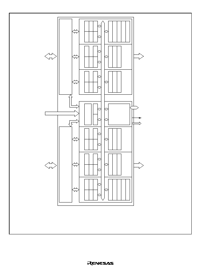
Rev. 2.0, 04/02, page 504 of 906
Channel 3
TMDR
TIORL
TSR
TCR
TIORH
TIER
TGRA
TCNT
TGRB
TGRC
TGRD
Channel 4
TMDR
TSR
TCR
TIOR
TIER
TGRA
TCNT
TGRB
Control logic
TMDR
TSR
TCR
TIOR
TIER
TGRA
TCNT
TGRB
Control logic for channels 3 to 5
TMDR
TSR
TCR
TIOR
TIER
TGRA
TCNT
TGRB
TGRC
Channel 1
TMDR
TSR
TCR
TIOR
TIER
TGRA
TCNT
TGRB
Channel 0
TMDR
TSR
TCR
TIORH
TIER
Control logic for channels 0 to 2
TGRA
TCNT
TGRB
TGRD
TSYR
TSTR
Input/output pins
TIOCA3
TIOCB3
TIOCC3
TIOCD3
TIOCA4
TIOCB4
TIOCA5
TIOCB5
Clock input
¯/1
¯/4
¯/16
¯/64
¯/256
¯/1024
¯/4096
TCLKA
TCLKB
TCLKC
TCLKD
Input/output pins
TIOCA0
TIOCB0
TIOCC0
TIOCD0
TIOCA1
TIOCB1
TIOCA2
TIOCB2
Interrupt request signals
Channel 3:
Channel 4:
Channel 5:
Interrupt request signals
Channel 0:
Channel 1:
Channel 2:
Internal data bus
A/D conversion start request signal
PPG output trigger signal
TIORL
Module data bus
TGI3A
TGI3B
TGI3C
TGI3D
TCI3V
TGI4A
TGI4B
TCI4V
TCI4U
TGI5A
TGI5B
TCI5V
TCI5U
TGI0A
TGI0B
TGI0C
TGI0D
TCI0V
TGI1A
TGI1B
TCI1V
TCI1U
TGI2A
TGI2B
TCI2V
TCI2U
Channel 3:
Channel 4:
Channel 5:
Internal clock:
External clock:
Channel 0:
Channel 1:
Channel 2:
Legend
TSTR:
Timer start register
TSYR:
Timer synchronous register
TCR:
Timer control register
TMDR:
Timer mode register
TIOR (H, L): Timer I/O control registers (H, L)
TIER:
Timer interrupt enable register
TSR:
Timer status register
TGR (A, B, C, D): Timer general registers (A, B, C, D)
TCNT:
Timer counter
Channel 2
Common
Channel 5
Bus interface
Figure 11.1 Block Diagram of TPU

Rev. 2.0, 04/02, page 505 of 906
11.2
Input/Output Pins
Table 11.2
Pin Configuration
Channel
Symbol
I/O
Function
All
TCLKA
Input
External clock A input pin
(Channel 1 and 5 phase counting mode A phase input)
TCLKB
Input
External clock B input pin
(Channel 1 and 5 phase counting mode B phase input)
TCLKC
Input
External clock C input pin
(Channel 2 and 4 phase counting mode A phase input)
TCLKD
Input
External clock D input pin
(Channel 2 and 4 phase counting mode B phase input)
0
TIOCA0
I/O
TGRA_0 input capture input/output compare output/PWM output pin
TIOCB0
I/O
TGRB_0 input capture input/output compare output/PWM output pin
TIOCC0
I/O
TGRC_0 input capture input/output compare output/PWM output pin
TIOCD0
I/O
TGRD_0 input capture input/output compare output/PWM output pin
1
TIOCA1
I/O
TGRA_1 input capture input/output compare output/PWM output pin
TIOCB1
I/O
TGRB_1 input capture input/output compare output/PWM output pin
2
TIOCA2
I/O
TGRA_2 input capture input/output compare output/PWM output pin
TIOCB2
I/O
TGRB_2 input capture input/output compare output/PWM output pin
3
TIOCA3
I/O
TGRA_3 input capture input/output compare output/PWM output pin
TIOCB3
I/O
TGRB_3 input capture input/output compare output/PWM output pin
TIOCC3
I/O
TGRC_3 input capture input/output compare output/PWM output pin
TIOCD3
I/O
TGRD_3 input capture input/output compare output/PWM output pin
4
TIOCA4
I/O
TGRA_4 input capture input/output compare output/PWM output pin
TIOCB4
I/O
TGRB_4 input capture input/output compare output/PWM output pin
5
TIOCA5
I/O
TGRA_5 input capture input/output compare output/PWM output pin
TIOCB5
I/O
TGRB_5 input capture input/output compare output/PWM output pin

Rev. 2.0, 04/02, page 506 of 906
11.3
Register Descriptions
The TPU has the following registers in each channel.
∑
Timer control register_0 (TCR_0)
∑
Timer mode register_0 (TMDR_0)
∑
Timer I/O control register H_0 (TIORH_0)
∑
Timer I/O control register L_0 (TIORL_0)
∑
Timer interrupt enable register_0 (TIER_0)
∑
Timer status register_0 (TSR_0)
∑
Timer counter_0 (TCNT_0)
∑
Timer general register A_0 (TGRA_0)
∑
Timer general register B_0 (TGRB_0)
∑
Timer general register C_0 (TGRC_0)
∑
Timer general register D_0 (TGRD_0)
∑
Timer control register_1 (TCR_1)
∑
Timer mode register_1 (TMDR_1)
∑
Timer I/O control register _1 (TIOR_1)
∑
Timer interrupt enable register_1 (TIER_1)
∑
Timer status register_1 (TSR_1)
∑
Timer counter_1 (TCNT_1)
∑
Timer general register A_1 (TGRA_1)
∑
Timer general register B_1 (TGRB_1)
∑
Timer control register_2 (TCR_2)
∑
Timer mode register_2 (TMDR_2)
∑
Timer I/O control register_2 (TIOR_2)
∑
Timer interrupt enable register_2 (TIER_2)
∑
Timer status register_2 (TSR_2)
∑
Timer counter_2 (TCNT_2)
∑
Timer general register A_2 (TGRA_2)
∑
Timer general register B_2 (TGRB_2)
∑
Timer control register_3 (TCR_3)
∑
Timer mode register_3 (TMDR_3)
∑
Timer I/O control register H_3 (TIORH_3)
∑
Timer I/O control register L_3 (TIORL_3)
∑
Timer interrupt enable register_3 (TIER_3)
∑
Timer status register_3 (TSR_3)
∑
Timer counter_3 (TCNT_3)

Rev. 2.0, 04/02, page 507 of 906
∑
Timer general register A_3 (TGRA_3)
∑
Timer general register B_3 (TGRB_3)
∑
Timer general register C_3 (TGRC_3)
∑
Timer general register D_3 (TGRD_3)
∑
Timer control register_4 (TCR_4)
∑
Timer mode register_4 (TMDR_4)
∑
Timer I/O control register _4 (TIOR_4)
∑
Timer interrupt enable register_4 (TIER_4)
∑
Timer status register_4 (TSR_4)
∑
Timer counter_4 (TCNT_4)
∑
Timer general register A_4 (TGRA_4)
∑
Timer general register B_4 (TGRB_4)
∑
Timer control register_5 (TCR_5)
∑
Timer mode register_5 (TMDR_5)
∑
Timer I/O control register_5 (TIOR_5)
∑
Timer interrupt enable register_5 (TIER_5)
∑
Timer status register_5 (TSR_5)
∑
Timer counter_5 (TCNT_5)
∑
Timer general register A_5 (TGRA_5)
∑
Timer general register B_5 (TGRB_5)
Common Registers
∑
Timer start register (TSTR)
∑
Timer synchronous register (TSYR)
11.3.1
Timer Control Register (TCR)
The TCR registers control the TCNT operation for each channel. The TPU has a total of six TCR
registers, one for each channel. TCR register settings should be made only when TCNT operation
is stopped.

Rev. 2.0, 04/02, page 508 of 906
Bit
Bit Name
Initial Value
R/W
Description
7
6
5
CCLR2
CCLR1
CCLR0
0
0
0
R/W
R/W
R/W
Counter Clear 2 to 0
These bits select the TCNT counter clearing source.
See tables 11.3 and 11.4 for details.
4
3
CKEG1
CKEG0
0
0
R/W
R/W
Clock Edge 1 and 0
These bits select the input clock edge. When the
input clock is counted using both edges, the input
clock period is halved (e.g. ¯/4 both edges = ¯/2
rising edge). If phase counting mode is used on
channels 1, 2, 4, and 5, this setting is ignored and the
phase counting mode setting has priority. Internal
clock edge selection is valid when the input clock is
¯/4 or slower. This setting is ignored if the input clock
is ¯/1, or when overflow/underflow of another
channel is selected.
00: Count at rising edge
01: Count at falling edge
1x: Count at both edges
Legend: x: Don't care
2
1
0
TPSC2
TPSC1
TPSC0
0
0
0
R/W
R/W
R/W
Time Prescaler 2 to 0
These bits select the TCNT counter clock. The clock
source can be selected independently for each
channel. See tables 11.5 to 11.10 for details.

Rev. 2.0, 04/02, page 509 of 906
Table 11.3
CCLR2 to CCLR0 (Channels 0 and 3)
Channel
Bit 7
CCLR2
Bit 6
CCLR1
Bit 5
CCLR0
Description
0, 3
0
0
0
TCNT clearing disabled
1
TCNT cleared by TGRA compare match/input
capture
1
0
TCNT cleared by TGRB compare match/input
capture
1
TCNT cleared by counter clearing for another
channel performing synchronous clearing/
synchronous operation
*
1
1
0
0
TCNT clearing disabled
1
TCNT cleared by TGRC compare match/input
capture
*
2
1
0
TCNT cleared by TGRD compare match/input
capture
*
2
1
TCNT cleared by counter clearing for another
channel performing synchronous clearing/
synchronous operation
*
1
Notes: 1. Synchronous operation setting is performed by setting the SYNC bit in TSYR to 1.
2. When TGRC or TGRD is used as a buffer register, TCNT is not cleared because the
buffer register setting has priority, and compare match/input capture does not occur.
Table 11.4
CCLR2 to CCLR0 (Channels 1, 2, 4, and 5)
Channel
Bit 7
Reserved
*
2
Bit 6
CCLR1
Bit 5
CCLR0
Description
1, 2, 4, 5
0
0
0
TCNT clearing disabled
1
TCNT cleared by TGRA compare match/input
capture
1
0
TCNT cleared by TGRB compare match/input
capture
1
TCNT cleared by counter clearing for another
channel performing synchronous clearing/
synchronous operation
*
1
Notes: 1. Synchronous operation setting is performed by setting the SYNC bit in TSYR to 1.
2. Bit 7 is reserved in channels 1, 2, 4, and 5. It is always read as 0 and cannot be
modified.

Rev. 2.0, 04/02, page 510 of 906
Table 11.5
TPSC2 to TPSC0 (Channel 0)
Channel
Bit 2
TPSC2
Bit 1
TPSC1
Bit 0
TPSC0
Description
0
0
0
0
Internal clock: counts on ¯/1
1
Internal clock: counts on ¯/4
1
0
Internal clock: counts on ¯/16
1
Internal clock: counts on ¯/64
1
0
0
External clock: counts on TCLKA pin input
1
External clock: counts on TCLKB pin input
1
0
External clock: counts on TCLKC pin input
1
External clock: counts on TCLKD pin input
Table 11.6
TPSC2 to TPSC0 (Channel 1)
Channel
Bit 2
TPSC2
Bit 1
TPSC1
Bit 0
TPSC0
Description
1
0
0
0
Internal clock: counts on ¯/1
1
Internal clock: counts on ¯/4
1
0
Internal clock: counts on ¯/16
1
Internal clock: counts on ¯/64
1
0
0
External clock: counts on TCLKA pin input
1
External clock: counts on TCLKB pin input
1
0
Internal clock: counts on ¯/256
1
Counts on TCNT2 overflow/underflow
Note: This setting is ignored when channel 1 is in phase counting mode.

Rev. 2.0, 04/02, page 511 of 906
Table 11.7
TPSC2 to TPSC0 (Channel 2)
Channel
Bit 2
TPSC2
Bit 1
TPSC1
Bit 0
TPSC0
Description
2
0
0
0
Internal clock: counts on ¯/1
1
Internal clock: counts on ¯/4
1
0
Internal clock: counts on ¯/16
1
Internal clock: counts on ¯/64
1
0
0
External clock: counts on TCLKA pin input
1
External clock: counts on TCLKB pin input
1
0
External clock: counts on TCLKC pin input
1
Internal clock: counts on ¯/1024
Note: This setting is ignored when channel 2 is in phase counting mode.
Table 11.8
TPSC2 to TPSC0 (Channel 3)
Channel
Bit 2
TPSC2
Bit 1
TPSC1
Bit 0
TPSC0
Description
3
0
0
0
Internal clock: counts on ¯/1
1
Internal clock: counts on ¯/4
1
0
Internal clock: counts on ¯/16
1
Internal clock: counts on ¯/64
1
0
0
External clock: counts on TCLKA pin input
1
Internal clock: counts on ¯/1024
1
0
Internal clock: counts on ¯/256
1
Internal clock: counts on ¯/4096

Rev. 2.0, 04/02, page 512 of 906
Table 11.9
TPSC2 to TPSC0 (Channel 4)
Channel
Bit 2
TPSC2
Bit 1
TPSC1
Bit 0
TPSC0
Description
4
0
0
0
Internal clock: counts on ¯/1
1
Internal clock: counts on ¯/4
1
0
Internal clock: counts on ¯/16
1
Internal clock: counts on ¯/64
1
0
0
External clock: counts on TCLKA pin input
1
External clock: counts on TCLKC pin input
1
0
Internal clock: counts on ¯/1024
1
Counts on TCNT5 overflow/underflow
Note: This setting is ignored when channel 4 is in phase counting mode.
Table 11.10 TPSC2 to TPSC0 (Channel 5)
Channel
Bit 2
TPSC2
Bit 1
TPSC1
Bit 0
TPSC0
Description
5
0
0
0
Internal clock: counts on ¯/1
1
Internal clock: counts on ¯/4
1
0
Internal clock: counts on ¯/16
1
Internal clock: counts on ¯/64
1
0
0
External clock: counts on TCLKA pin input
1
External clock: counts on TCLKC pin input
1
0
Internal clock: counts on ¯/256
1
External clock: counts on TCLKD pin input
Note: This setting is ignored when channel 5 is in phase counting mode.

Rev. 2.0, 04/02, page 513 of 906
11.3.2
Timer Mode Register (TMDR)
TMDR registers are used to set the operating mode for each channel. The TPU has six TMDR
registers, one for each channel. TMDR register settings should be made only when TCNT
operation is stopped.
Bit
Bit Name
Initial Value
R/W
Description
7
6
≠
≠
1
1
≠
≠
Reserved
These bits are always read as 1 and cannot be
modified.
5
BFB
0
R/W
Buffer Operation B
Specifies whether TGRB is to operate in the normal
way, or TGRB and TGRD are to be used together for
buffer operation. When TGRD is used as a buffer
register, TGRD input capture/output compare is not
generated.
In channels 1, 2, 4, and 5, which have no TGRD, bit
5 is reserved. It is always read as 0 and cannot be
modified.
0: TGRB operates normally
1: TGRB and TGRD used together for buffer
operation
4
BFA
0
R/W
Buffer Operation A
Specifies whether TGRA is to operate in the normal
way, or TGRA and TGRC are to be used together for
buffer operation. When TGRC is used as a buffer
register, TGRC input capture/output compare is not
generated.
In channels 1, 2, 4, and 5, which have no TGRC, bit
4 is reserved. It is always read as 0 and cannot be
modified.
0: TGRA operates normally
1: TGRA and TGRC used together for buffer
operation
3
2
1
0
MD3
MD2
MD1
MD0
0
0
0
0
R/W
R/W
R/W
R/W
Modes 3 to 0
These bits are used to set the timer operating mode.
MD3 is a reserved bit. In a write, it should always be
written with 0. See table 11.11 for details.

Rev. 2.0, 04/02, page 514 of 906
Table 11.11 MD3 to MD0
Bit 3
MD3
*
1
Bit 2
MD2
*
2
Bit 1
MD1
Bit 0
MD0
Description
0
0
0
0
Normal operation
1
Reserved
1
0
PWM mode 1
1
PWM mode 2
1
0
0
Phase counting mode 1
1
Phase counting mode 2
1
0
Phase counting mode 3
1
Phase counting mode 4
1
x
x
x
--
Legend: x: Don't care
Notes: 1. MD3 is a reserved bit. In a write, it should always be written with 0.
2. Phase counting mode cannot be set for channels 0 and 3. In this case, 0 should always
be written to MD2.
11.3.3
Timer I/O Control Register (TIOR)
TIOR registers control the TGR registers. The TPU has eight TIOR registers, two each for
channels 0 and 3, and one each for channels 1, 2, 4, and 5. Care is required since TIOR is affected
by the TMDR setting.
The initial output specified by TIOR is valid when the counter is stopped (the CST bit in TSTR is
cleared to 0). Note also that, in PWM mode 2, the output at the point at which the counter is
cleared to 0 is specified.
When TGRC or TGRD is designated for buffer operation, this setting is invalid and the register
operates as a buffer register.

Rev. 2.0, 04/02, page 515 of 906
TIORH_0, TIOR_1, TIOR_2, TIORH_3, TIOR_4, TIOR_5
Bit
Bit Name
Initial
Value
R/W
Description
7
6
5
4
IOB3
IOB2
IOB1
IOB0
0
0
0
0
R/W
R/W
R/W
R/W
I/O Control B3 to B0
Specify the function of TGRB.
For details, see tables 11.12, 11.14, 11.15, 11.16,
11.18, and 11.19.
3
2
1
0
IOA3
IOA2
IOA1
IOA0
0
0
0
0
R/W
R/W
R/W
R/W
I/O Control A3 to A0
Specify the function of TGRA.
For details, see tables 11.20, 11.22, 11.23, 11.24,
11.26, and 11.27.
TIORL_0, TIORL_3
Bit
Bit Name
Initial
Value
R/W
Description
7
6
5
4
IOD3
IOD2
IOD1
IOD0
0
0
0
0
R/W
R/W
R/W
R/W
I/O Control D3 to D0
Specify the function of TGRD.
For details, see tables 11.13, and 11.17.
3
2
1
0
IOC3
IOC2
IOC1
IOC0
0
0
0
0
R/W
R/W
R/W
R/W
I/O Control C3 to C0
Specify the function of TGRC.
For details, see tables 11.21, and 11.25

Rev. 2.0, 04/02, page 516 of 906
Table 11.12 TIORH_0
Description
Bit 7
IOB3
Bit 6
IOB2
Bit 5
IOB1
Bit 4
IOB0
TGRB_0
Function
TIOCB0 Pin Function
0
0
0
0
Output
Output disabled
1
compare
register
Initial output is 0 output
0 output at compare match
1
0
Initial output is 0 output
1 output at compare match
1
Initial output is 0 output
Toggle output at compare match
1
0
0
Output disabled
1
Initial output is 1 output
0 output at compare match
1
0
Initial output is 1 output
1 output at compare match
1
Initial output is 1 output
Toggle output at compare match
1
0
0
0
Capture input source is TIOCB0 pin
Input capture at rising edge
1
Capture input source is TIOCB0 pin
Input capture at falling edge
1
x
Input
capture
register
Capture input source is TIOCB0 pin
Input capture at both edges
1
x
x
Capture input source is channel 1/count clock
Input capture at TCNT_1 count- up/count-down
*
Legend: x: Don't care
Note: When bits TPSC2 to TPSC0 in TCR_1 are set to B'000 and ¯/1 is used as the TCNT_1
count clock, this setting is invalid and input capture is not generated.

Rev. 2.0, 04/02, page 517 of 906
Table 11.13 TIORL_0
Description
Bit 7
IOD3
Bit 6
IOD2
Bit 5
IOD1
Bit 4
IOD0
TGRD_0
Function
TIOCD0 Pin Function
0
0
0
0
Output disabled
1
Output
compare
register
*
2
Initial output is 0 output
0 output at compare match
1
0
Initial output is 0 output
1 output at compare match
1
Initial output is 0 output
Toggle output at compare match
1
0
0
Output disabled
1
Initial output is 1 output
0 output at compare match
1
0
Initial output is 1 output
1 output at compare match
1
Initial output is 1 output
Toggle output at compare match
1
0
0
0
Capture input source is TIOCD0 pin
Input capture at rising edge
1
Capture input source is TIOCD0 pin
Input capture at falling edge
1
x
Input
capture
register
*
2
Capture input source is TIOCD0 pin
Input capture at both edges
1
x
x
Capture input source is channel 1/count clock
Input capture at TCNT_1 count-up/count-down
*
1
Legend: x: Don't care
Notes: 1. When bits TPSC2 to TPSC0 in TCR_1 are set to B'000 and ¯/1 is used as the TCNT_1
count clock, this setting is invalid and input capture is not generated.
2. When the BFB bit in TMDR_0 is set to 1 and TGRD_0 is used as a buffer register, this
setting is invalid and input capture/output compare is not generated.

Rev. 2.0, 04/02, page 518 of 906
Table 11.14 TIOR_1
Description
Bit 7
IOB3
Bit 6
IOB2
Bit 5
IOB1
Bit 4
IOB0
TGRB_1
Function
TIOCB1 Pin Function
0
0
0
0
Output disabled
1
Output
compare
register
Initial output is 0 output
0 output at compare match
1
0
Initial output is 0 output
1 output at compare match
1
Initial output is 0 output
Toggle output at compare match
1
0
0
Output disabled
1
Initial output is 1 output
0 output at compare match
1
0
Initial output is 1 output
1 output at compare match
1
Initial output is 1 output
Toggle output at compare match
1
0
0
0
Capture input source is TIOCB1 pin
Input capture at rising edge
1
Capture input source is TIOCB1 pin
Input capture at falling edge
1
x
Input
capture
register
Capture input source is TIOCB1 pin
Input capture at both edges
1
x
x
TGRC_0 compare match/input capture
Input capture at generation of TGRC_0 compare
match/input capture
Legend: x: Don't care

Rev. 2.0, 04/02, page 519 of 906
Table 11.15 TIOR_2
Description
Bit 7
IOB3
Bit 6
IOB2
Bit 5
IOB1
Bit 4
IOB0
TGRB_2
Function
TIOCB2 Pin Function
0
0
0
0
Output disabled
1
Output
compare
register
Initial output is 0 output
0 output at compare match
1
0
Initial output is 0 output
1 output at compare match
1
Initial output is 0 output
Toggle output at compare match
1
0
0
Output disabled
1
Initial output is 1 output
0 output at compare match
1
0
Initial output is 1 output
1 output at compare match
1
Initial output is 1 output
Toggle output at compare match
1
x
0
0
Capture input source is TIOCB2 pin
Input capture at rising edge
1
Capture input source is TIOCB2 pin
Input capture at falling edge
1
x
Input
capture
register
Capture input source is TIOCB2 pin
Input capture at both edges
Legend: x: Don't care

Rev. 2.0, 04/02, page 520 of 906
Table 11.16 TIORH_3
Description
Bit 7
IOB3
Bit 6
IOB2
Bit 5
IOB1
Bit 4
IOB0
TGRB_3
Function
TIOCB3 Pin Function
0
0
0
0
Output disabled
1
Output
compare
register
Initial output is 0 output
0 output at compare match
1
0
Initial output is 0 output
1 output at compare match
1
Initial output is 0 output
Toggle output at compare match
1
0
0
Output disabled
1
Initial output is 1 output
0 output at compare match
1
0
Initial output is 1 output
1 output at compare match
1
Initial output is 1 output
Toggle output at compare match
1
0
0
0
Capture input source is TIOCB3 pin
Input capture at rising edge
1
Capture input source is TIOCB3 pin
Input capture at falling edge
1
x
Input
capture
register
Capture input source is TIOCB3 pin
Input capture at both edges
1
x
x
Capture input source is channel 4/count clock
Input capture at TCNT_4 count-up/count-down
*
Legend: x: Don't care
Note: When bits TPSC2 to TPSC0 in TCR_4 are set to B'000 and ¯/1 is used as the TCNT_4
count clock, this setting is invalid and input capture is not generated.

Rev. 2.0, 04/02, page 521 of 906
Table 11.17 TIORL_3
Description
Bit 7
IOD3
Bit 6
IOD2
Bit 5
IOD1
Bit 4
IOD0
TGRD_3
Function
TIOCD3 Pin Function
0
0
0
0
Output disabled
1
Output
compare
register
*
2
Initial output is 0 output
0 output at compare match
1
0
Initial output is 0 output
1 output at compare match
1
Initial output is 0 output
Toggle output at compare match
1
0
0
Output disabled
1
Initial output is 1 output
0 output at compare match
1
0
Initial output is 1 output
1 output at compare match
1
Initial output is 1 output
Toggle output at compare match
1
0
0
0
Capture input source is TIOCD3 pin
Input capture at rising edge
1
Capture input source is TIOCD3 pin
Input capture at falling edge
1
x
Input
capture
register
*
2
Capture input source is TIOCD3 pin
Input capture at both edges
1
x
x
Capture input source is channel 4/count clock
Input capture at TCNT_4 count-up/count-down
*
1
Legend: x: Don't care
Notes: 1. When bits TPSC2 to TPSC0 in TCR_4 are set to B'000 and ¯/1 is used as the TCNT_4
count clock, this setting is invalid and input capture is not generated.
2. When the BFB bit in TMDR_3 is set to 1 and TGRD_3 is used as a buffer register, this
setting is invalid and input capture/output compare is not generated.

Rev. 2.0, 04/02, page 522 of 906
Table 11.18 TIOR_4
Description
Bit 7
IOB3
Bit 6
IOB2
Bit 5
IOB1
Bit 4
IOB0
TGRB_4
Function
TIOCB4 Pin Function
0
0
0
0
Output disabled
1
Output
compare
register
Initial output is 0 output
0 output at compare match
1
0
Initial output is 0 output
1 output at compare match
1
Initial output is 0 output
Toggle output at compare match
1
0
0
Output disabled
1
Initial output is 1 output
0 output at compare match
1
0
Initial output is 1 output
1 output at compare match
1
Initial output is 1 output
Toggle output at compare match
1
0
0
0
Capture input source is TIOCB4 pin
Input capture at rising edge
1
Capture input source is TIOCB4 pin
Input capture at falling edge
1
x
Input
capture
register
Capture input source is TIOCB4 pin
Input capture at both edges
1
x
x
Capture input source is TGRC_3 compare
match/input capture
Input capture at generation of TGRC_3 compare
match/input capture
Legend: x: Don't care

Rev. 2.0, 04/02, page 523 of 906
Table 11.19 TIOR_5
Description
Bit 7
IOB3
Bit 6
IOB2
Bit 5
IOB1
Bit 4
IOB0
TGRB_5
Function
TIOCB5 Pin Function
0
0
0
0
Output disabled
1
Output
compare
register
Initial output is 0 output
0 output at compare match
1
0
Initial output is 0 output
1 output at compare match
1
Initial output is 0 output
Toggle output at compare match
1
0
0
Output disabled
1
Initial output is 1 output
0 output at compare match
1
0
Initial output is 1 output
1 output at compare match
1
Initial output is 1 output
Toggle output at compare match
1
x
0
0
Capture input source is TIOCB5 pin
Input capture at rising edge
1
Capture input source is TIOCB5 pin
Input capture at falling edge
1
x
Input
capture
register
Capture input source is TIOCB5 pin
Input capture at both edges
Legend: x: Don't care

Rev. 2.0, 04/02, page 524 of 906
Table 11.20 TIORH_0
Description
Bit 3
IOA3
Bit 2
IOA2
Bit 1
IOA1
Bit 0
IOA0
TGRA_0
Function
TIOCA0 Pin Function
0
0
0
0
Output disabled
1
Output
compare
register
Initial output is 0 output
0 output at compare match
1
0
Initial output is 0 output
1 output at compare match
1
Initial output is 0 output
Toggle output at compare match
1
0
0
Output disabled
1
Initial output is 1 output
0 output at compare match
1
0
Initial output is 1 output
1 output at compare match
1
Initial output is 1 output
Toggle output at compare match
1
0
0
0
Capture input source is TIOCA0 pin
Input capture at rising edge
1
Capture input source is TIOCA0 pin
Input capture at falling edge
1
x
Input
capture
register
Capture input source is TIOCA0 pin
Input capture at both edges
1
x
x
Capture input source is channel 1/count clock
Input capture at TCNT_1 count-up/count-down
Legend: x: Don't care

Rev. 2.0, 04/02, page 525 of 906
Table 11.21 TIORL_0
Description
Bit 3
IOC3
Bit 2
IOC2
Bit 1
IOC1
Bit 0
IOC0
TGRC_0
Function
TIOCC0 Pin Function
0
0
0
0
Output disabled
1
Output
compare
register
*
Initial output is 0 output
0 output at compare match
1
0
Initial output is 0 output
1 output at compare match
1
Initial output is 0 output
Toggle output at compare match
1
0
0
Output disabled
1
Initial output is 1 output
0 output at compare match
1
0
Initial output is 1 output
1 output at compare match
1
Initial output is 1 output
Toggle output at compare match
1
0
0
0
Capture input source is TIOCC0 pin
Input capture at rising edge
1
Capture input source is TIOCC0 pin
Input capture at falling edge
1
x
Input
capture
register
*
Capture input source is TIOCC0 pin
Input capture at both edges
1
x
x
Capture input source is channel 1/count clock
Input capture at TCNT_1 count-up/count-down
Legend: x: Don't care
Note: When the BFA bit in TMDR_0 is set to 1 and TGRC_0 is used as a buffer register, this
setting is invalid and input capture/output compare is not generated.

Rev. 2.0, 04/02, page 526 of 906
Table 11.22 TIOR_1
Description
Bit 3
IOA3
Bit 2
IOA2
Bit 1
IOA1
Bit 0
IOA0
TGRA_1
Function
TIOCA1 Pin Function
0
0
0
0
Output disabled
1
Output
compare
register
Initial output is 0 output
0 output at compare match
1
0
Initial output is 0 output
1 output at compare match
1
Initial output is 0 output
Toggle output at compare match
1
0
0
Output disabled
1
Initial output is 1 output
0 output at compare match
1
0
Initial output is 1 output
1 output at compare match
1
Initial output is 1 output
Toggle output at compare match
1
0
0
0
Capture input source is TIOCA1 pin
Input capture at rising edge
1
Capture input source is TIOCA1 pin
Input capture at falling edge
1
x
Input
capture
register
Capture input source is TIOCA1 pin
Input capture at both edges
1
x
x
Capture input source is TGRA_0 compare
match/input capture
Input capture at generation of channel 0/TGRA_0
compare match/input capture
Legend: x: Don't care

Rev. 2.0, 04/02, page 527 of 906
Table 11.23 TIOR_2
Description
Bit 3
IOA3
Bit 2
IOA2
Bit 1
IOA1
Bit 0
IOA0
TGRA_2
Function
TIOCA2 Pin Function
0
0
0
0
Output disabled
1
Output
compare
register
Initial output is 0 output
0 output at compare match
1
0
Initial output is 0 output
1 output at compare match
1
Initial output is 0 output
Toggle output at compare match
1
0
0
Output disabled
1
Initial output is 1 output
0 output at compare match
1
0
Initial output is 1 output
1 output at compare match
1
Initial output is 1 output
Toggle output at compare match
1
x
0
0
Capture input source is TIOCA2 pin
Input capture at rising edge
1
Capture input source is TIOCA2 pin
Input capture at falling edge
1
x
Input
capture
register
Capture input source is TIOCA2 pin
Input capture at both edges
Legend: x: Don't care

Rev. 2.0, 04/02, page 528 of 906
Table 11.24 TIORH_3
Description
Bit 3
IOA3
Bit 2
IOA2
Bit 1
IOA1
Bit 0
IOA0
TGRA_3
Function
TIOCA3 Pin Function
0
0
0
0
Output disabled
1
Output
compare
register
Initial output is 0 output
0 output at compare match
1
0
Initial output is 0 output
1 output at compare match
1
Initial output is 0 output
Toggle output at compare match
1
0
0
Output disabled
1
Initial output is 1 output
0 output at compare match
1
0
Initial output is 1 output
1 output at compare match
1
Initial output is 1 output
Toggle output at compare match
1
0
0
0
Capture input source is TIOCA3 pin
Input capture at rising edge
1
Capture input source is TIOCA3 pin
Input capture at falling edge
1
x
Input
capture
register
Capture input source is TIOCA3 pin
Input capture at both edges
1
x
x
Capture input source is channel 4/count clock
Input capture at TCNT_4 count-up/count-down
Legend: x: Don't care

Rev. 2.0, 04/02, page 529 of 906
Table 11.25 TIORL_3
Description
Bit 3
IOC3
Bit 2
IOC2
Bit 1
IOC1
Bit 0
IOC0
TGRC_3
Function
TIOCC3 Pin Function
0
0
0
0
Output disabled
1
Output
compare
register
*
Initial output is 0 output
0 output at compare match
1
0
Initial output is 0 output
1 output at compare match
1
Initial output is 0 output
Toggle output at compare match
1
0
0
Output disabled
1
Initial output is 1 output
0 output at compare match
1
0
Initial output is 1 output
1 output at compare match
1
Initial output is 1 output
Toggle output at compare match
1
0
0
0
Capture input source is TIOCC3 pin
Input capture at rising edge
1
Capture input source is TIOCC3 pin
Input capture at falling edge
1
x
Input
capture
register
*
Capture input source is TIOCC3 pin
Input capture at both edges
1
x
x
Capture input source is channel 4/count clock
Input capture at TCNT_4 count-up/count-down
Legend: x: Don't care
Note: When the BFA bit in TMDR_3 is set to 1 and TGRC_3 is used as a buffer register, this
setting is invalid and input capture/output compare is not generated.

Rev. 2.0, 04/02, page 530 of 906
Table 11.26 TIOR_4
Description
Bit 3
IOA3
Bit 2
IOA2
Bit 1
IOA1
Bit 0
IOA0
TGRA_4
Function
TIOCA4 Pin Function
0
0
0
0
Output disabled
1
Output
compare
register
Initial output is 0 output
0 output at compare match
1
0
Initial output is 0 output
1 output at compare match
1
Initial output is 0 output
Toggle output at compare match
1
0
0
Output disabled
1
Initial output is 1 output
0 output at compare match
1
0
Initial output is 1 output
1 output at compare match
1
Initial output is 1 output
Toggle output at compare match
1
0
0
0
Capture input source is TIOCA4 pin
Input capture at rising edge
1
Capture input source is TIOCA4 pin
Input capture at falling edge
1
x
Input
capture
register
Capture input source is TIOCA4 pin
Input capture at both edges
1
x
x
Capture input source is TGRA_3 compare
match/input capture
Input capture at generation of TGRA_3 compare
match/input capture
Legend: x: Don't care

Rev. 2.0, 04/02, page 531 of 906
Table 11.27 TIOR_5
Description
Bit 3
IOA3
Bit 2
IOA2
Bit 1
IOA1
Bit 0
IOA0
TGRA_5
Function
TIOCA5 Pin Function
0
0
0
0
Output disabled
1
Output
compare
register
Initial output is 0 output
0 output at compare match
1
0
Initial output is 0 output
1 output at compare match
1
Initial output is 0 output
Toggle output at compare match
1
0
0
Output disabled
1
Initial output is 1 output
0 output at compare match
1
0
Initial output is 1 output
1 output at compare match
1
Initial output is 1 output
Toggle output at compare match
1
x
0
0
Input capture source is TIOCA5 pin
Input capture at rising edge
1
Input capture source is TIOCA5 pin
Input capture at falling edge
1
x
Input
capture
register
Input capture source is TIOCA5 pin
Input capture at both edges
Legend: x: Don't care

Rev. 2.0, 04/02, page 532 of 906
11.3.4
Timer Interrupt Enable Register (TIER)
TIER registers control enabling or disabling of interrupt requests for each channel. The TPU has
six TIER registers, one for each channel.
Bit
Bit Name
Initial value
R/W
Description
7
TTGE
0
R/W
A/D Conversion Start Request Enable
Enables or disables generation of A/D conversion
start requests by TGRA input capture/compare
match.
0: A/D conversion start request generation disabled
1: A/D conversion start request generation enabled
6
≠
1
≠
Reserved
This bit is always read as 1 and cannot be modified.
5
TCIEU
0
R/W
Underflow Interrupt Enable
Enables or disables interrupt requests (TCIU) by the
TCFU flag when the TCFU flag in TSR is set to 1 in
channels 1, 2, 4, and 5.
In channels 0 and 3, bit 5 is reserved. It is always
read as 0 and cannot be modified.
0: Interrupt requests (TCIU) by TCFU disabled
1: Interrupt requests (TCIU) by TCFU enabled
4
TCIEV
0
R/W
Overflow Interrupt Enable
Enables or disables interrupt requests (TCIV) by the
TCFV flag when the TCFV flag in TSR is set to 1.
0: Interrupt requests (TCIV) by TCFV disabled
1: Interrupt requests (TCIV) by TCFV enabled
3
TGIED
0
R/W
TGR Interrupt Enable D
Enables or disables interrupt requests (TGID) by the
TGFD bit when the TGFD bit in TSR is set to 1 in
channels 0 and 3.
In channels 1, 2, 4, and 5, bit 3 is reserved. It is
always read as 0 and cannot be modified.
0: Interrupt requests (TGID) by TGFD bit disabled
1: Interrupt requests (TGID) by TGFD bit enabled

Rev. 2.0, 04/02, page 533 of 906
Bit
Bit Name
Initial value
R/W
Description
2
TGIEC
0
R/W
TGR Interrupt Enable C
Enables or disables interrupt requests (TGIC) by the
TGFC bit when the TGFC bit in TSR is set to 1 in
channels 0 and 3.
In channels 1, 2, 4, and 5, bit 2 is reserved. It is
always read as 0 and cannot be modified.
0: Interrupt requests (TGIC) by TGFC bit disabled
1: Interrupt requests (TGIC) by TGFC bit enabled
1
TGIEB
0
R/W
TGR Interrupt Enable B
Enables or disables interrupt requests (TGIB) by the
TGFB bit when the TGFB bit in TSR is set to 1.
0: Interrupt requests (TGIB) by TGFB bit disabled
1: Interrupt requests (TGIB) by TGFB bit enabled
0
TGIEA
0
R/W
TGR Interrupt Enable A
Enables or disables interrupt requests (TGIA) by the
TGFA bit when the TGFA bit in TSR is set to 1.
0: Interrupt requests (TGIA) by TGFA bit disabled
1: Interrupt requests (TGIA) by TGFA bit enabled

Rev. 2.0, 04/02, page 534 of 906
11.3.5
Timer Status Register (TSR)
TSR registers indicate the status of each channel. The TPU has six TSR registers, one for each
channel.
Bit
Bit Name
Initial value
R/W
Description
7
TCFD
1
R
Count Direction Flag
Status flag that shows the direction in which TCNT
counts in channels 1, 2, 4, and 5.
In channels 0 and 3, bit 7 is reserved. It is always
read as 1 and cannot be modified.
0: TCNT counts down
1: TCNT counts up
6
≠
1
≠
Reserved
This bit is always read as 1 and cannot be modified.
5
TCFU
0
R/(W)
*
Underflow Flag
Status flag that indicates that TCNT underflow has
occurred when channels 1, 2, 4, and 5 are set to
phase counting mode.
In channels 0 and 3, bit 5 is reserved. It is always
read as 0 and cannot be modified.
[Setting condition]
When the TCNT value underflows (changes from
H'0000 to H'FFFF)
[Clearing condition]
When 0 is written to TCFU after reading TCFU = 1
4
TCFV
0
R/(W)
*
Overflow Flag
Status flag that indicates that TCNT overflow has
occurred.
[Setting condition]
When the TCNT value overflows (changes from
H'FFFF to H'0000)
[Clearing condition]
When 0 is written to TCFV after reading TCFV = 1

Rev. 2.0, 04/02, page 535 of 906
Bit
Bit Name
Initial value
R/W
Description
3
TGFD
0
R/(W)
*
Input Capture/Output Compare Flag D
Status flag that indicates the occurrence of TGRD
input capture or compare match in channels 0 and 3.
In channels 1, 2, 4, and 5, bit 3 is reserved. It is
always read as 0 and cannot be modified.
[Setting conditions]
∑
When TCNT = TGRD while TGRD is functioning
as output compare register
∑
When TCNT value is transferred to TGRD by
input capture signal while TGRD is functioning as
input capture register
[Clearing conditions]
∑
When DTC is activated by TGID interrupt while
DISEL bit of MRB in DTC is 0
∑
When 0 is written to TGFD after reading TGFD =
1
2
TGFC
0
R/(W)
*
Input Capture/Output Compare Flag C
Status flag that indicates the occurrence of TGRC
input capture or compare match in channels 0 and 3.
In channels 1, 2, 4, and 5, bit 2 is reserved. It is
always read as 0 and cannot be modified.
[Setting conditions]
∑
When TCNT = TGRC while TGRC is functioning
as output compare register
∑
When TCNT value is transferred to TGRC by
input capture signal while TGRC is functioning as
input capture register
[Clearing conditions]
∑
When DTC is activated by TGIC interrupt while
DISEL bit of MRB in DTC is 0
∑
When 0 is written to TGFC after reading TGFC =
1

Rev. 2.0, 04/02, page 536 of 906
Bit
Bit Name
Initial value
R/W
Description
1
TGFB
0
R/(W)
*
Input Capture/Output Compare Flag B
Status flag that indicates the occurrence of TGRB
input capture or compare match.
[Setting conditions]
∑
When TCNT = TGRB while TGRB is functioning
as output compare register
∑
When TCNT value is transferred to TGRB by
input capture signal while TGRB is functioning as
input capture register
[Clearing conditions]
∑
When DTC is activated by TGIB interrupt while
DISEL bit of MRB in DTC is 0
∑
When 0 is written to TGFB after reading TGFB =
1
0
TGFA
0
R/(W)
*
Input Capture/Output Compare Flag A
Status flag that indicates the occurrence of TGRA
input capture or compare match.
[Setting conditions]
∑
When TCNT = TGRA while TGRA is functioning
as output compare register
∑
When TCNT value is transferred to TGRA by
input capture signal while TGRA is functioning as
input capture register
[Clearing conditions]
∑
When DTC is activated by TGIA interrupt while
DISEL bit of MRB in DTC is 0
∑
When 0 is written to TGFA after reading TGFA =
1
Note: Only 0 can be written, for flag clearing.
11.3.6
Timer Counter (TCNT)
The TCNT registers are 16-bit readable/writable counters. The TPU has six TCNT counters, one
for each channel.
The TCNT counters are initialized to H'0000 by a reset, or in hardware standby mode.
The TCNT counters cannot be accessed in 8-bit units; they must always be accessed as a 16-bit
unit.

Rev. 2.0, 04/02, page 537 of 906
11.3.7
Timer General Register (TGR)
The TGR registers are 16-bit readable/writable registers with a dual function as output compare
and input capture registers. The TPU has 16 TGR registers, four each for channels 0 and 3 and two
each for channels 1, 2, 4, and 5. TGRC and TGRD for channels 0 and 3 can also be designated for
operation as buffer registers. The TGR registers cannot be accessed in 8-bit units; they must
always be accessed as a 16-bit unit. TGR buffer register combinations are TGRA≠TGRC and
TGRB≠TGRD.
11.3.8
Timer Start Register (TSTR)
TSTR selects operation/stoppage for channels 0 to 5. When setting the operating mode in TMDR
or setting the count clock in TCR, first stop the TCNT counter.
Bit
Bit Name
Initial value
R/W
Description
7
6
≠
0
≠
Reserved
These bits should always be written with 0.
5
4
3
2
1
0
CST5
CST4
CST3
CST2
CST1
CST0
0
0
0
0
0
0
R/W
R/W
R/W
R/W
R/W
R/W
Counter Start 5 to 0
These bits select operation or stoppage for TCNT.
If 0 is written to the CST bit during operation with the
TIOC pin designated for output, the counter stops but
the TIOC pin output compare output level is retained.
If TIOR is written to when the CST bit is cleared to 0,
the pin output level will be changed to the set initial
output value.
0: TCNT_5 to TCNT_0 count operation is stopped
1: TCNT_5 to TCNT_0 performs count operation

Rev. 2.0, 04/02, page 538 of 906
11.3.9
Timer Synchronous Register (TSYR)
TSYR selects independent operation or synchronous operation for the TCNT counters of channels
0 to 5. A channel performs synchronous operation when the corresponding bit in TSYR is set to 1.
Bit
Bit Name
Initial value
R/W
Description
7
6
≠
≠
≠
≠
R/W
R/W
Reserved
These bits should always be written with 0.
5
4
3
2
1
0
SYNC5
SYNC4
SYNC3
SYNC2
SYNC1
SYNC0
0
0
0
0
0
0
R/W
R/W
R/W
R/W
R/W
R/W
Timer Synchronization 5 to 0
These bits select whether operation is independent of
or synchronized with other channels.
When synchronous operation is selected,
synchronous presetting of multiple channels, and
synchronous clearing through counter clearing on
another channel are possible.
To set synchronous operation, the SYNC bits for at
least two channels must be set to 1. To set
synchronous clearing, in addition to the SYNC bit, the
TCNT clearing source must also be set by means of
bits CCLR2 to CCLR0 in TCR.
0: TCNT_5 to TCNT_0 operates independently
(TCNT presetting /clearing is unrelated to
other channels)
1: TCNT_5 to TCNT_0 performs synchronous
operation (TCNT synchronous presetting/
synchronous clearing is possible)
Rev. 2.0, 04/02, page 539 of 906
11.4
Operation
11.4.1
Basic Functions
Each channel has a TCNT and TGR register. TCNT performs up-counting, and is also capable of
free-running operation, periodic counting, and external event counting.
Each TGR can be used as an input capture register or output compare register.
Counter Operation: When one of bits CST0 to CST5 is set to 1 in TSTR, the TCNT counter for
the corresponding channel starts counting. TCNT can operate as a free-running counter, periodic
counter, and so on.
1. Example of count operation setting procedure
Figure 11.2 shows an example of the count operation setting procedure.
Select counter clock
Operation selection
Select counter clearing source
Periodic counter
Set period
Start count
<Periodic counter>
[1]
[2]
[4]
[3]
[5]
Free-running counter
Start count
<Free-running counter>
[5]
[1]
[2]
[3]
[4]
[5]
Select output compare register
Select the counter
clock with bits
TPSC2 to TPSC0 in
TCR. At the same
time, select the
input clock edge
with bits CKEG1
and CKEG0 in TCR.
For periodic counter
operation, select the
TGR to be used as
the TCNT clearing
source with bits
CCLR2 to CCLR0 in
TCR.
Designate the TGR
selected in [2] as an
output compare
register by means of
TIOR.
Set the periodic
counter cycle in the
TGR selected in [2].
Set the CST bit in
TSTR to 1 to start
the counter
operation.
Figure 11.2 Example of Counter Operation Setting Procedure
Rev. 2.0, 04/02, page 540 of 906
2. Free-running count operation and periodic count operation
Immediately after a reset, the TPU's TCNT counters are all designated as free-running
counters. When the relevant bit in TSTR is set to 1 the corresponding TCNT counter starts up-
count operation as a free-running counter. When TCNT overflows (changes from H'FFFF to
H'0000), the TCFV bit in TSR is set to 1. If the value of the corresponding TCIEV bit in TIER
is 1 at this point, the TPU requests an interrupt. After overflow, TCNT starts counting up again
from H'0000.
Figure 11.3 illustrates free-running counter operation.
TCNT value
H'FFFF
H'0000
CST bit
TCFV
Time
Figure 11.3 Free-Running Counter Operation
When compare match is selected as the TCNT clearing source, the TCNT counter for the
relevant channel performs periodic count operation. The TGR register for setting the period is
designated as an output compare register, and counter clearing by compare match is selected
by means of bits CCLR2 to CCLR0 in TCR. After the settings have been made, TCNT starts
count-up operation as a periodic counter when the corresponding bit in TSTR is set to 1. When
the count value matches the value in TGR, the TGF bit in TSR is set to 1 and TCNT is cleared
to H'0000.
If the value of the corresponding TGIE bit in TIER is 1 at this point, the TPU requests an
interrupt. After a compare match, TCNT starts counting up again from H'0000.
Figure 11.4 illustrates periodic counter operation.
Rev. 2.0, 04/02, page 541 of 906
TCNT value
TGR
H'0000
CST bit
TGF
Time
Counter cleared by TGR
compare match
Flag cleared by software or
DTC activation
Figure 11.4 Periodic Counter Operation
Waveform Output by Compare Match: The TPU can perform 0, 1, or toggle output from the
corresponding output pin using a compare match.
1. Example of setting procedure for waveform output by compare match
Figure 11.5 shows an example of the setting procedure for waveform output by a compare
match.
Select waveform output mode
Output selection
Set output timing
Start count
<Waveform output>
[1]
[2]
[3]
[1] Select initial value 0 output or 1 output, and
compare match output value 0 output, 1 output,
or toggle output, by means of TIOR. The set
initial value is output at the TIOC pin until the
first compare match occurs.
[2] Set the timing for compare match generation in
TGR.
[3] Set the CST bit in TSTR to 1 to start the count
operation.
Figure 11.5 Example of Setting Procedure for Waveform Output by Compare Match

Rev. 2.0, 04/02, page 542 of 906
2. Examples of waveform output operation
Figure 11.6 shows an example of 0 output/1 output.
In this example, TCNT has been designated as a free-running counter, and settings have been
made so that 1 is output by compare match A, and 0 is output by compare match B. When the
set level and the pin level match, the pin level does not change.
TCNT value
H'FFFF
H'0000
TIOCA
TIOCB
Time
TGRA
TGRB
No change
No change
No change
No change
1 output
0 output
Figure 11.6 Example of 0 Output/1 Output Operation
Figure 11.7 shows an example of toggle output.
In this example TCNT has been designated as a periodic counter (with counter clearing
performed by compare match B), and settings have been made so that output is toggled by both
compare match A and compare match B.
TCNT value
H'FFFF
H'0000
TIOCB
TIOCA
Time
TGRB
TGRA
Toggle output
Toggle output
Counter cleared by TGRB compare match
Figure 11.7 Example of Toggle Output Operation
Rev. 2.0, 04/02, page 543 of 906
Input Capture Function: The TCNT value can be transferred to TGR on detection of the TIOC
pin input edge.
Rising edge, falling edge, or both edges can be selected as the detection edge. For channels 0, 1, 3,
and 4, it is also possible to specify another channel's counter input clock or compare match signal
as the input capture source.
Note:
When another channel's counter input clock is used as the input capture input for channels
0 and 3, ¯/1 should not be selected as the counter input clock used for input capture input.
Input capture will not be generated if ¯/1 is selected.
1. Example of setting procedure for input capture operation
Figure 11.8 shows an example of the setting procedure for input capture operation.
Select input capture input
Input selection
Start count
<Input capture operation>
[1]
[2]
[1] Designate TGR as an input capture register by
means of TIOR, and select the input capture
source and input signal edge (rising edge, falling
edge, or both edges).
[2] Set the CST bit in TSTR to 1 to start the count
operation.
Figure 11.8 Example of Setting Procedure for Input Capture Operation
2. Example of input capture operation
Figure 11.9 shows an example of input capture operation.
In this example both rising and falling edges have been selected as the TIOCA pin input
capture input edge, falling edge has been selected as the TIOCB pin input capture input edge,
and counter clearing by TGRB input capture has been designated for TCNT.
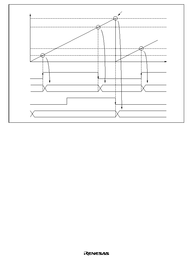
Rev. 2.0, 04/02, page 544 of 906
TCNT value
H'0180
H'0000
TIOCA
TGRA
Time
H'0010
H'0005
Counter cleared by TIOCB
input (falling edge)
H'0160
H'0005
H'0160
H'0010
TGRB
H'0180
TIOCB
Figure 11.9 Example of Input Capture Operation
11.4.2
Synchronous Operation
In synchronous operation, the values in multiple TCNT counters can be rewritten simultaneously
(synchronous presetting). Also, multiple of TCNT counters can be cleared simultaneously
(synchronous clearing) by making the appropriate setting in TCR.
Synchronous operation enables TGR to be incremented with respect to a single time base.
Channels 0 to 5 can all be designated for synchronous operation.
Example of Synchronous Operation Setting Procedure: Figure 11.10 shows an example of the
synchronous operation setting procedure.
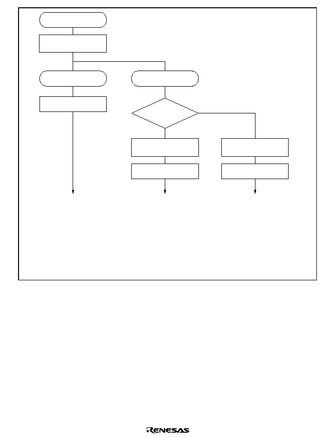
Rev. 2.0, 04/02, page 545 of 906
Synchronous operation
selection
Set TCNT
Synchronous presetting
<Synchronous presetting>
[1]
[2]
Synchronous clearing
Select counter
clearing source
<Counter clearing>
[3]
Start count
[5]
Set synchronous
counter clearing
<Synchronous clearing>
[4]
Start count
[5]
Clearing
source generation
channel?
No
Yes
[1] Set to 1 the SYNC bits in TSYR corresponding to the channels to be designated for synchronous operation.
[2] When the TCNT counter of any of the channels designated for synchronous operation is written to, the
same value is simultaneously written to the other TCNT counters.
[3] Use bits CCLR2 to CCLR0 in TCR to specify TCNT clearing by input capture/output compare, etc.
[4] Use bits CCLR2 to CCLR0 in TCR to designate synchronous clearing for the counter clearing source.
[5] Set to 1 the CST bits in TSTR for the relevant channels, to start the count operation.
Set synchronous
operation
Figure 11.10 Example of Synchronous Operation Setting Procedure
Example of Synchronous Operation: Figure 11.11 shows an example of synchronous operation.
In this example, synchronous operation and PWM mode 1 have been designated for channels 0 to
2, TGRB_0 compare match has been set as the channel 0 counter clearing source, and
synchronous clearing has been set for the channel 1 and 2 counter clearing source.
Three-phase PWM waveforms are output from pins TIOCA0, TIOCA1, and TIOCA2. At this
time, synchronous presetting, and synchronous clearing by TGRB_0 compare match, is performed
for channel 0 to 2 TCNT counters, and the data set in TGRB_0 is used as the PWM cycle.
For details on PWM modes, see section 11.4.5, PWM Modes.
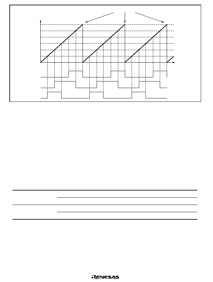
Rev. 2.0, 04/02, page 546 of 906
TCNT0 to TCNT2 values
H'0000
TIOCA_0
TIOCA_1
TGRB_0
Synchronous clearing by TGRB_0 compare match
TGRA_2
TGRA_1
TGRB_2
TGRA_0
TGRB_1
TIOCA_2
Time
Figure 11.11 Example of Synchronous Operation
11.4.3
Buffer Operation
Buffer operation, provided for channels 0 and 3, enables TGRC and TGRD to be used as buffer
registers.
Buffer operation differs depending on whether TGR has been designated as an input capture
register or a compare match register.
Table 11.28 shows the register combinations used in buffer operation.
Table 11.28 Register Combinations in Buffer Operation
Channel
Timer General Register
Buffer Register
0
TGRA_0
TGRC_0
TGRB_0
TGRD_0
3
TGRA_3
TGRC_3
TGRB_3
TGRD_3
∑
When TGR is an output compare register
When a compare match occurs, the value in the buffer register for the corresponding channel is
transferred to the timer general register.
This operation is illustrated in figure 11.12.
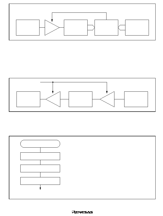
Rev. 2.0, 04/02, page 547 of 906
Buffer register
Timer general
register
TCNT
Comparator
Compare match signal
Figure 11.12 Compare Match Buffer Operation
∑
When TGR is an input capture register
When input capture occurs, the value in TCNT is transferred to TGR and the value previously
held in the timer general register is transferred to the buffer register.
This operation is illustrated in figure 11.13.
Buffer register
Timer general
register
TCNT
Input capture
signal
Figure 11.13 Input Capture Buffer Operation
Example of Buffer Operation Setting Procedure: Figure 11.14 shows an example of the buffer
operation setting procedure.
Select TGR function
Buffer operation
Set buffer operation
Start count
<Buffer operation>
[1]
[2]
[3]
[1] Designate TGR as an input capture register or
output compare register by means of TIOR.
[2] Designate TGR for buffer operation with bits
BFA and BFB in TMDR.
[3] Set the CST bit in TSTR to 1 to start the count
operation.
Figure 11.14 Example of Buffer Operation Setting Procedure

Rev. 2.0, 04/02, page 548 of 906
Examples of Buffer Operation:
1. When TGR is an output compare register
Figure 11.15 shows an operation example in which PWM mode 1 has been designated for
channel 0, and buffer operation has been designated for TGRA and TGRC. The settings used
in this example are TCNT clearing by compare match B, 1 output at compare match A, and 0
output at compare match B.
As buffer operation has been set, when compare match A occurs the output changes and the
value in buffer register TGRC is simultaneously transferred to timer general register TGRA.
This operation is repeated each time compare match A occurs.
For details on PWM modes, see section 11.4.5, PWM Modes.
TCNT value
TGRB_0
H'0000
TGRC_0
TGRA_0
H'0200
H'0520
TIOCA
H'0200
H'0450
H'0520
H'0450
TGRA_0
H'0450
H'0200
Transfer
Time
Figure 11.15 Example of Buffer Operation (1)
2. When TGR is an input capture register
Figure 11.16 shows an operation example in which TGRA has been designated as an input
capture register, and buffer operation has been designated for TGRA and TGRC.
Counter clearing by TGRA input capture has been set for TCNT, and both rising and falling
edges have been selected as the TIOCA pin input capture input edge.
As buffer operation has been set, when the TCNT value is stored in TGRA upon occurrence of
input capture A, the value previously stored in TGRA is simultaneously transferred to TGRC.
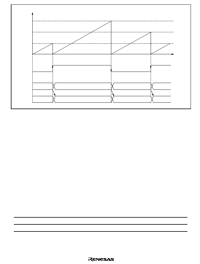
Rev. 2.0, 04/02, page 549 of 906
TCNT value
H'09FB
H'0000
TGRC
Time
H'0532
TIOCA
TGRA
H'0F07
H'0532
H'0F07
H'0532
H'0F07
H'09FB
Figure 11.16 Example of Buffer Operation (2)
11.4.4
Cascaded Operation
In cascaded operation, two 16-bit counters for different channels are used together as a 32-bit
counter.
This function works by counting the channel 1 (channel 4) counter clock at overflow/underflow of
TCNT_2 (TCNT_5) as set in bits TPSC2 to TPSC0 in TCR.
Underflow occurs only when the lower 16-bit TCNT is in phase-counting mode.
Table 11.29 shows the register combinations used in cascaded operation.
Note: When phase counting mode is set for channel 1 or 4, the counter clock setting is invalid
and the counter operates independently in phase counting mode.
Table 11.29 Cascaded Combinations
Combination
Upper 16 Bits
Lower 16 Bits
Channels 1 and 2
TCNT_1
TCNT_2
Channels 4 and 5
TCNT_4
TCNT_5
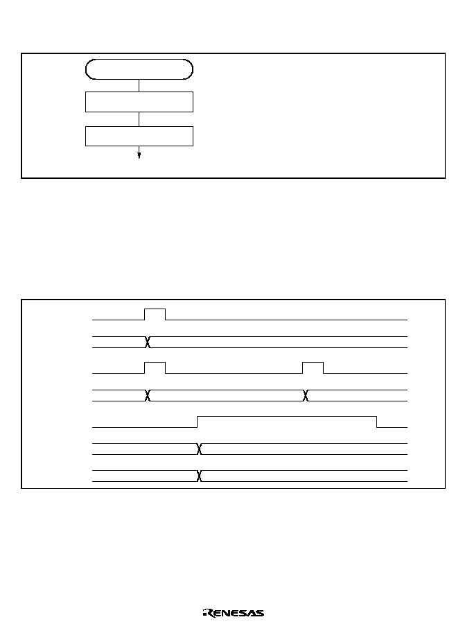
Rev. 2.0, 04/02, page 550 of 906
Example of Cascaded Operation Setting Procedure: Figure 11.17 shows an example of the
setting procedure for cascaded operation.
Cascaded operation
Set cascading
Start count
<Cascaded operation>
Set bits TPSC2 to TPSC0 in the channel 1
(channel 4) TCR to B'1111 to select TCNT_2
(TCNT_5) overflow/underflow counting.
Set the CST bit in TSTR for the upper and lower
channel to 1 to start the count operation.
[1]
[2]
[1]
[2]
Figure 11.17 Cascaded Operation Setting Procedure
Examples of Cascaded Operation: Figure 11.18 illustrates the operation when counting upon
TCNT_2 overflow/underflow has been set for TCNT_1, TGRA_1 and TGRA_2 have been
designated as input capture registers, and the TIOC pin rising edge has been selected.
When a rising edge is input to the TIOCA1 and TIOCA2 pins simultaneously, the upper 16 bits of
the 32-bit data are transferred to TGRA_1, and the lower 16 bits to TGRA_2.
TCNT_2
clock
TCNT_2
H'FFFF
H'0000
H'0001
TIOCA1,
TIOCA2
TGRA_1
H'03A2
TGRA_2
H'0000
TCNT_1
clock
TCNT_1
H'03A1
H'03A2
Figure 11.18 Example of Cascaded Operation (1)
Figure 11.19 illustrates the operation when counting upon TCNT_2 overflow/underflow has been
set for TCNT_1, and phase counting mode has been designated for channel 2.
TCNT_1 is incremented by TCNT_2 overflow and decremented by TCNT_2 underflow.
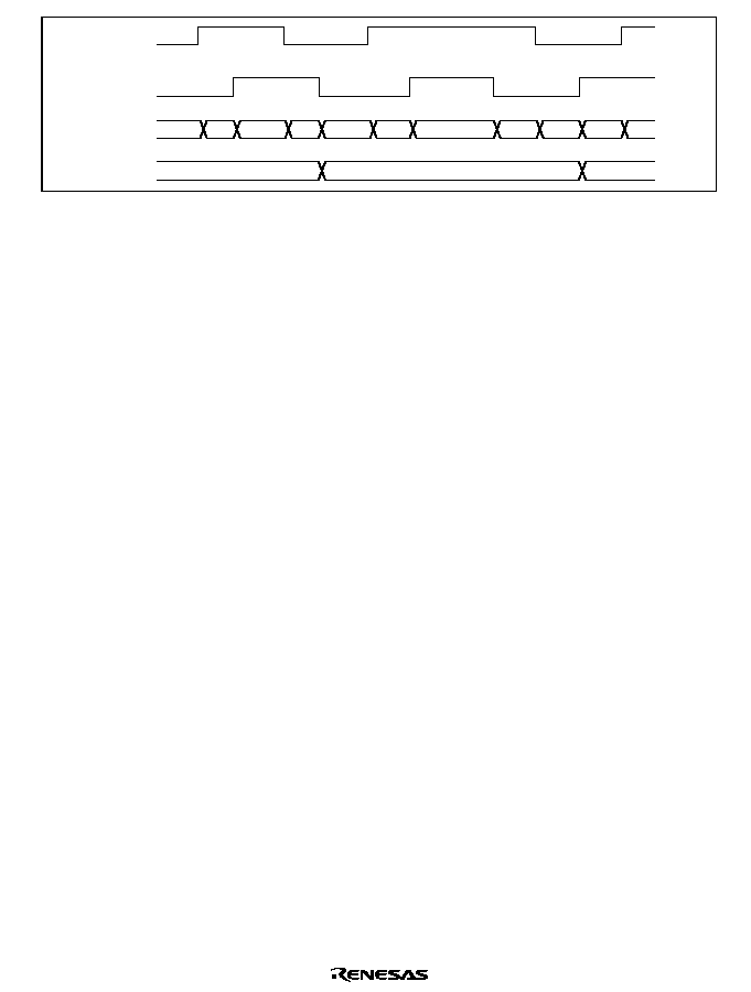
Rev. 2.0, 04/02, page 551 of 906
TCLKC
TCNT_2
FFFD
TCNT_1
0001
TCLKD
FFFE
FFFF
0000
0001
0002
0001
0000
FFFF
0000
0000
Figure 11.19 Example of Cascaded Operation (2)
11.4.5
PWM Modes
In PWM mode, PWM waveforms are output from the output pins. 0, 1, or toggle output can be
selected as the output level in response to compare match of each TGR.
Settings of TGR registers can output a PWM waveform in the range of 0≠% to 100≠% duty cycle.
Designating TGR compare match as the counter clearing source enables the cycle to be set in that
register. All channels can be designated for PWM mode independently. Synchronous operation is
also possible.
There are two PWM modes, as described below.
∑
PWM mode 1
PWM output is generated from the TIOCA and TIOCC pins by pairing TGRA with TGRB and
TGRC with TGRD. The outputs specified by bits IOA3 to IOA0 and IOC3 to IOC0 in TIOR
are output from the TIOCA and TIOCC pins at compare matches A and C, respectively. The
outputs specified by bits IOB3 to IOB0 and IOD3 to IOD0 in TIOR are output at compare
matches B and D, respectively. The initial output value is the value set in TGRA or TGRC. If
the set values of paired TGRs are identical, the output value does not change when a compare
match occurs.
In PWM mode 1, a maximum 8-phase PWM output is possible.
∑
PWM mode 2
PWM output is generated using one TGR as the cycle register and the others as duty cycle
registers. The output specified in TIOR is performed by means of compare matches. Upon
counter clearing by a synchronization register compare match, the output value of each pin is
the initial value set in TIOR. If the set values of the cycle and duty cycle registers are identical,
the output value does not change when a compare match occurs.
In PWM mode 2, a maximum 15-phase PWM output is possible by combined use with
synchronous operation.
The correspondence between PWM output pins and registers is shown in table 11.30.

Rev. 2.0, 04/02, page 552 of 906
Table 11.30 PWM Output Registers and Output Pins
Output Pins
Channel
Registers
PWM Mode 1
PWM Mode 2
0
TGRA_0
TIOCA0
TIOCA0
TGRB_0
TIOCB0
TGRC_0
TIOCC0
TIOCC0
TGRD_0
TIOCD0
1
TGRA_1
TIOCA1
TIOCA1
TGRB_1
TIOCB1
2
TGRA_2
TIOCA2
TIOCA2
TGRB_2
TIOCB2
3
TGRA_3
TIOCA3
TIOCA3
TGRB_3
TIOCB3
TGRC_3
TIOCC3
TIOCC3
TGRD_3
TIOCD3
4
TGRA_4
TIOCA4
TIOCA4
TGRB_4
TIOCB4
5
TGRA_5
TIOCA5
TIOCA5
TGRB_5
TIOCB5
Note: In PWM mode 2, PWM output is not possible for the TGR register in which the cycle is set.
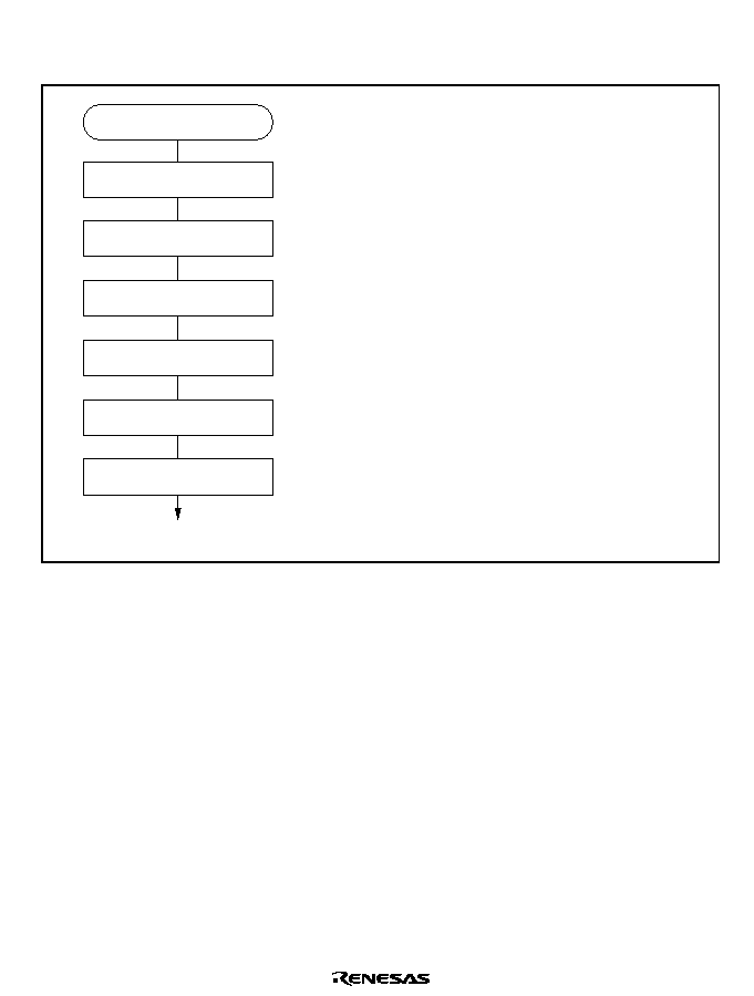
Rev. 2.0, 04/02, page 553 of 906
Example of PWM Mode Setting Procedure: Figure 11.20 shows an example of the PWM mode
setting procedure.
Select counter clock
PWM mode
Select counter clearing source
Select waveform output level
<PWM mode>
[1]
[2]
[3]
Set TGR
[4]
Set PWM mode
[5]
Start count
[6]
[1] Select the counter clock with bits TPSC2 to
TPSC0 in TCR. At the same time, select the
input clock edge with bits CKEG1 and CKEG0 in
TCR.
[2] Use bits CCLR2 to CCLR0 in TCR to select the
TGR to be used as the TCNT clearing source.
[3] Use TIOR to designate the TGR as an output
compare register, and select the initial value and
output value.
[4] Set the cycle in the TGR selected in [2], and
set the duty in the other TGRs.
[5] Select the PWM mode with bits MD3 to MD0 in
TMDR.
[6] Set the CST bit in TSTR to 1 to start the count
operation.
Figure 11.20 Example of PWM Mode Setting Procedure
Examples of PWM Mode Operation: Figure 11.21 shows an example of PWM mode 1
operation.
In this example, TGRA compare match is set as the TCNT clearing source, 0 is set for the TGRA
initial output value and output value, and 1 is set as the TGRB output value.
In this case, the value set in TGRA is used as the cycle, and the values set in TGRB registers as
the duty cycle.
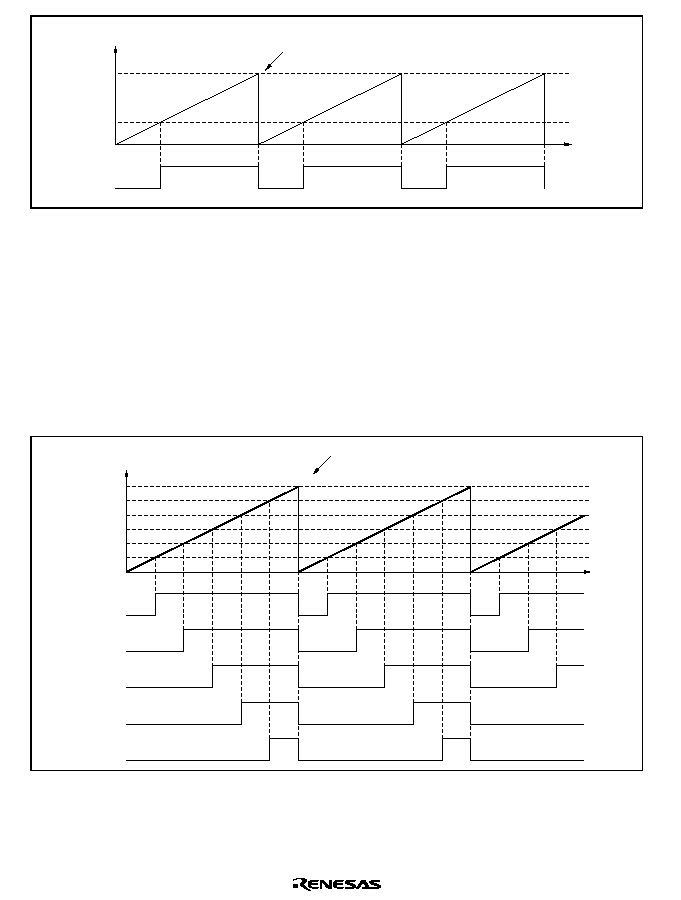
Rev. 2.0, 04/02, page 554 of 906
TCNT value
TGRA
H'0000
TIOCA
Time
TGRB
Counter cleared by
TGRA compare match
Figure 11.21 Example of PWM Mode Operation (1)
Figure 11.22 shows an example of PWM mode 2 operation.
In this example, synchronous operation is designated for channels 0 and 1, TGRB_1 compare
match is set as the TCNT clearing source, and 0 is set for the initial output value and 1 for the
output value of the other TGR registers (TGRA_0 to TGRD_0, TGRA_1), to output a 5-phase
PWM waveform.
In this case, the value set in TGRB_1 is used as the cycle, and the values set in the other TGRs as
the duty cycle.
TCNT value
TGRB_1
H'0000
TIOCA0
Counter cleared by
TGRB_1 compare match
Time
TGRA_1
TGRD_0
TGRC_0
TGRB_0
TGRA_0
TIOCB0
TIOCC0
TIOCD0
TIOCA1
Figure 11.22 Example of PWM Mode Operation (2)
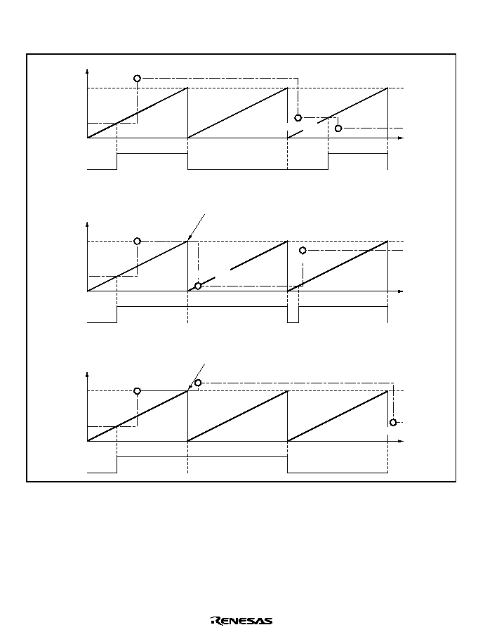
Rev. 2.0, 04/02, page 555 of 906
Figure 11.23 shows examples of PWM waveform output with 0% duty cycle and 100% duty cycle
in PWM mode.
TCNT value
TGRA
H'0000
TIOCA
Time
TGRB
0% duty
TGRB rewritten
TGRB
rewritten
TGRB rewritten
TCNT value
TGRA
H'0000
TIOCA
Time
TGRB
100% duty
TGRB rewritten
TGRB rewritten
TGRB rewritten
Output does not change when cycle register and duty register
compare matches occur simultaneously
TCNT value
TGRA
H'0000
TIOCA
Time
TGRB
100% duty
TGRB rewritten
TGRB rewritten
TGRB rewritten
Output does not change when cycle register and duty
register compare matches occur simultaneously
0% duty
Figure 11.23 Example of PWM Mode Operation (3)

Rev. 2.0, 04/02, page 556 of 906
11.4.6
Phase Counting Mode
In phase counting mode, the phase difference between two external clock inputs is detected and
TCNT is incremented/decremented accordingly. This mode can be set for channels 1, 2, 4, and 5.
When phase counting mode is set, an external clock is selected as the counter input clock and
TCNT operates as an up/down-counter regardless of the setting of bits TPSC2 to TPSC0 and bits
CKEG1 and CKEG0 in TCR. However, the functions of bits CCLR1 and CCLR0 in TCR, and of
TIOR, TIER, and TGR are valid, and input capture/compare match and interrupt functions can be
used.
This can be used for two-phase encoder pulse input.
When overflow occurs while TCNT is counting up, the TCFV flag in TSR is set; when underflow
occurs while TCNT is counting down, the TCFU flag is set.
The TCFD bit in TSR is the count direction flag. Reading the TCFD flag provides an indication of
whether TCNT is counting up or down.
Table 11.31 shows the correspondence between external clock pins and channels.
Table 11.31 Clock Input Pins in Phase Counting Mode
External Clock Pins
Channels
A-Phase
B-Phase
When channel 1 or 5 is set to phase counting mode
TCLKA
TCLKB
When channel 2 or 4 is set to phase counting mode
TCLKC
TCLKD
Example of Phase Counting Mode Setting Procedure: Figure 11.24 shows an example of the
phase counting mode setting procedure.
Phase counting mode
Select phase counting mode
Start count
<Phase counting mode>
Select phase counting mode with bits MD3 to
MD0 in TMDR.
Set the CST bit in TSTR to 1 to start the count
operation.
[1]
[2]
[1]
[2]
Figure 11.24 Example of Phase Counting Mode Setting Procedure
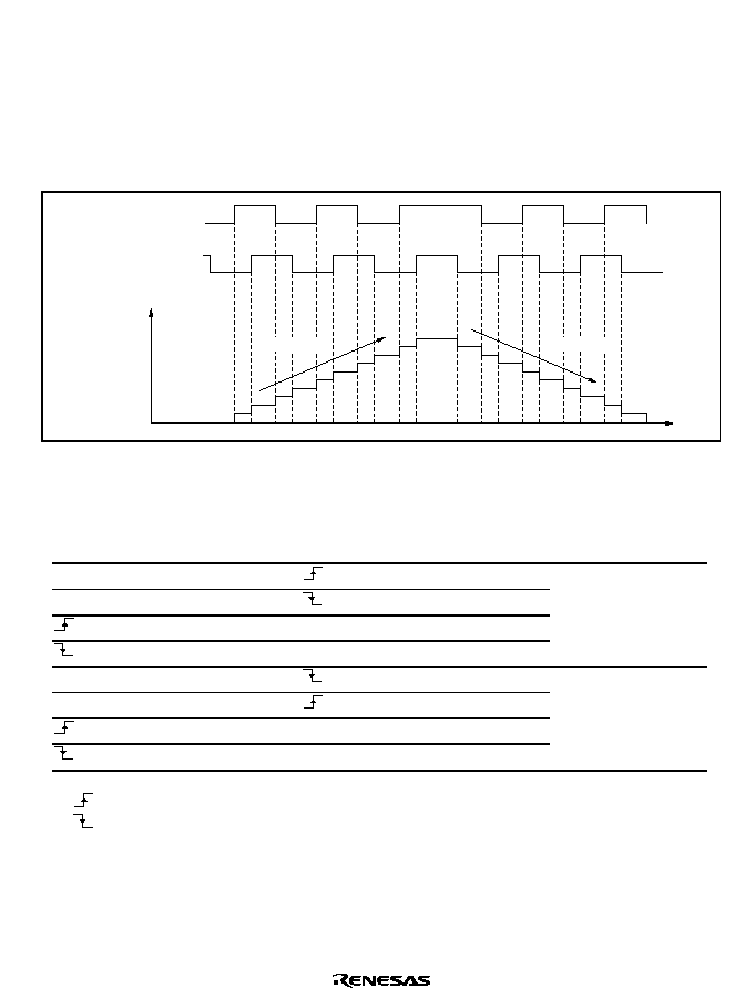
Rev. 2.0, 04/02, page 557 of 906
Examples of Phase Counting Mode Operation: In phase counting mode, TCNT counts up or
down according to the phase difference between two external clocks. There are four modes,
according to the count conditions.
1. Phase counting mode 1
Figure 11.25 shows an example of phase counting mode 1 operation, and table 11.32
summarizes the TCNT up/down-count conditions.
TCNT value
Time
Down-count
Up-count
TCLKA (channels 1 and 5)
TCLKC (channels 2 and 4)
TCLKB (channels 1 and 5)
TCLKD (channels 2 and 4)
Figure 11.25 Example of Phase Counting Mode 1 Operation
Table 11.32 Up/Down-Count Conditions in Phase Counting Mode 1
TCLKA (Channels 1 and 5)
TCLKC (Channels 2 and 4)
TCLKB (Channels 1 and 5)
TCLKD (Channels 2 and 4)
Operation
High level
Up-count
Low level
Low level
High level
High level
Down-count
Low level
High level
Low level
Legend
: Rising edge
: Falling edge

Rev. 2.0, 04/02, page 558 of 906
2. Phase counting mode 2
Figure 11.26 shows an example of phase counting mode 2 operation, and table 11.33
summarizes the TCNT up/down-count conditions.
Time
Down-count
Up-count
TCNT value
TCLKA (channels 1 and 5)
TCLKC (channels 2 and 4)
TCLKB (channels 1 and 5)
TCLKD (channels 2 and 4)
Figure 11.26 Example of Phase Counting Mode 2 Operation
Table 11.33 Up/Down-Count Conditions in Phase Counting Mode 2
TCLKA (Channels 1 and 5)
TCLKC (Channels 2 and 4)
TCLKB (Channels 1 and 5)
TCLKD (Channels 2 and 4)
Operation
High level
Don't care
Low level
Don't care
Low level
Don't care
High level
Up-count
High level
Don't care
Low level
Don't care
High level
Don't care
Low level
Down-count
Legend
: Rising edge
: Falling edge

Rev. 2.0, 04/02, page 559 of 906
3. Phase counting mode 3
Figure 11.27 shows an example of phase counting mode 3 operation, and table 11.34
summarizes the TCNT up/down-count conditions.
Time
Up-count
Down-count
TCNT value
TCLKA (channels 1 and 5)
TCLKC (channels 2 and 4)
TCLKB (channels 1 and 5)
TCLKD (channels 2 and 4)
Figure 11.27 Example of Phase Counting Mode 3 Operation
Table 11.34 Up/Down-Count Conditions in Phase Counting Mode 3
TCLKA (Channels 1 and 5)
TCLKC (Channels 2 and 4)
TCLKB (Channels 1 and 5)
TCLKD (Channels 2 and 4)
Operation
High level
Don't care
Low level
Don't care
Low level
Don't care
High level
Up-count
High level
Down-count
Low level
Don't care
High level
Don't care
Low level
Don't care
Legend
: Rising edge
: Falling edge
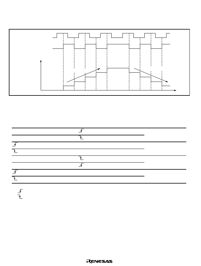
Rev. 2.0, 04/02, page 560 of 906
4. Phase counting mode 4
Figure 11.28 shows an example of phase counting mode 4 operation, and table 11.35
summarizes the TCNT up/down-count conditions.
Time
Up-count
Down-count
TCNT value
TCLKA (channels 1 and 5)
TCLKC (channels 2 and 4)
TCLKB (channels 1 and 5)
TCLKD (channels 2 and 4)
Figure 11.28 Example of Phase Counting Mode 4 Operation
Table 11.35 Up/Down-Count Conditions in Phase Counting Mode 4
TCLKA (Channels 1 and 5)
TCLKC (Channels 2 and 4)
TCLKB (Channels 1 and 5)
TCLKD (Channels 2 and 4)
Operation
High level
Up-count
Low level
Low level
Don't care
High level
High level
Down-count
Low level
High level
Don't care
Low level
Legend
: Rising edge
: Falling edge

Rev. 2.0, 04/02, page 561 of 906
Phase Counting Mode Application Example: Figure 11.29 shows an example in which phase
counting mode is designated for channel 1, and channel 1 is coupled with channel 0 to input servo
motor 2-phase encoder pulses in order to detect the position or speed.
Channel 1 is set to phase counting mode 1, and the encoder pulse A-phase and B-phase are input
to TCLKA and TCLKB.
Channel 0 operates with TCNT counter clearing by TGRC_0 compare match; TGRA_0 and
TGRC_0 are used for the compare match function, and are set with the speed control cycle and
position control cycle. TGRB_0 is used for input capture, with TGRB_0 and TGRD_0 operating
in buffer mode. The channel 1 counter input clock is designated as the TGRB_0 input capture
source, and detection of the pulse width of 2-phase encoder 4-multiplication pulses is performed.
TGRA_1 and TGRB_1 for channel 1 are designated for input capture, channel 0 TGRA_0 and
TGRC_0 compare matches are selected as the input capture source, and the up/down-counter
values for the control cycles are stored.
This procedure enables accurate position/speed detection to be achieved.
TCNT_1
TCNT_0
Channel 1
TGRA_1
(speed cycle capture)
TGRA_0
(speed control cycle)
TGRB_1
(position cycle capture)
TGRC_0
(position control cycle)
TGRB_0 (pulse width capture)
TGRD_0 (buffer operation)
Channel 0
TCLKA
TCLKB
Edge
detection
circuit
+
-
+
-
Figure 11.29 Phase Counting Mode Application Example

Rev. 2.0, 04/02, page 562 of 906
11.5
Interrupt Sources
There are three kinds of TPU interrupt source: TGR input capture/compare match, TCNT
overflow, and TCNT underflow. Each interrupt source has its own status flag and enable/disable
bit, allowing generation of interrupt request signals to be enabled or disabled individually.
When an interrupt request is generated, the corresponding status flag in TSR is set to 1. If the
corresponding enable/disable bit in TIER is set to 1 at this time, an interrupt is requested. The
interrupt request is cleared by clearing the status flag to 0.
Relative channel priorities can be changed by the interrupt controller, but the priority order within
a channel is fixed. For details, see section 5, Interrupt Controller.
Table 11.36 lists the TPU interrupt sources.

Rev. 2.0, 04/02, page 563 of 906
Table 11.36 TPU Interrupts
Channel Name
Interrupt Source
Interrupt
Flag
DTC
Activation
DMAC
Activation
0
TGI0A
TGRA_0 input capture/compare match TGFA_0
Possible
Possible
TGI0B
TGRB_0 input capture/compare match TGFB_0
Possible
Not possible
TGI0C
TGRC_0 input capture/compare match TGFC_0
Possible
Not possible
TGI0D
TGRD_0 input capture/compare match TGFD_0
Possible
Not possible
TGI0V
TCNT_0 overflow
TCFV_0
Not possible
Not possible
1
TGI1A
TGRA_1 input capture/compare match TGFA_1
Possible
Possible
TGI1B
TGRB_1 input capture/compare match TGFB_1
Possible
Not possible
TCI1V
TCNT_1 overflow
TCFV_1
Not possible
Not possible
TCI1U
TCNT_1 underflow
TCFU_1
Not possible
Not possible
2
TGI2A
TGRA_2 input capture/compare match TGFA_2
Possible
Possible
TGI2B
TGRB_2 input capture/compare match TGFB_2
Possible
Not possible
TCI2V
TCNT_2 overflow
TCFV_2
Not possible
Not possible
TCI2U
TCNT_2 underflow
TCFU_2
Not possible
Not possible
3
TGI3A
TGRA_3 input capture/compare match TGFA_3
Possible
Possible
TGI3B
TGRB_3 input capture/compare match TGFB_3
Possible
Not possible
TGI3C
TGRC_3 input capture/compare match TGFC_3
Possible
Not possible
TGI3D
TGRD_3 input capture/compare match TGFD_3
Possible
Not possible
TCI3V
TCNT_3 overflow
TCFV_3
Not possible
Not possible
4
TGI4A
TGRA_4 input capture/compare match TGFA_4
Possible
Possible
TGI4B
TGRB_4 input capture/compare match TGFB_4
Possible
Not possible
TCI4V
TCNT_4 overflow
TCFV_4
Not possible
Not possible
TCI4U
TCNT_4 underflow
TCFU_4
Not possible
Not possible
5
TGI5A
TGRA_5 input capture/compare match TGFA_5
Possible
Possible
TGI5B
TGRB_5 input capture/compare match TGFB_5
Possible
Not possible
TCI5V
TCNT_5 overflow
TCFV_5
Not possible
Not possible
TCI5U
TCNT_5 underflow
TCFU_5
Not possible
Not possible
Note: This table shows the initial state immediately after a reset. The relative channel priorities
can be changed by the interrupt controller.

Rev. 2.0, 04/02, page 564 of 906
Input Capture/Compare Match Interrupt: An interrupt is requested if the TGIE bit in TIER is
set to 1 when the TGF flag in TSR is set to 1 by the occurrence of a TGR input capture/compare
match on a particular channel. The interrupt request is cleared by clearing the TGF flag to 0. The
TPU has 16 input capture/compare match interrupts, four each for channels 0 and 3, and two each
for channels 1, 2, 4, and 5.
Overflow Interrupt: An interrupt is requested if the TCIEV bit in TIER is set to 1 when the
TCFV flag in TSR is set to 1 by the occurrence of TCNT overflow on a channel. The interrupt
request is cleared by clearing the TCFV flag to 0. The TPU has six overflow interrupts, one for
each channel.
Underflow Interrupt: An interrupt is requested if the TCIEU bit in TIER is set to 1 when the
TCFU flag in TSR is set to 1 by the occurrence of TCNT underflow on a channel. The interrupt
request is cleared by clearing the TCFU flag to 0. The TPU has four underflow interrupts, one
each for channels 1, 2, 4, and 5.
11.6
DTC Activation
The DTC can be activated by the TGR input capture/compare match interrupt for a channel. For
details, see section 9, Data Transfer Controller.
A total of 16 TPU input capture/compare match interrupts can be used as DTC activation sources,
four each for channels 0 and 3, and two each for channels 1, 2, 4, and 5.
11.7
DMAC Activation
The DMAC can be activated by the TGRA input capture/compare match interrupt for a channel.
For details, see section 7, DMA Controller.
In the TPU, a total of six TGRA input capture/compare match interrupts can be used as DMAC
activation sources, one for each channel.
11.8
A/D Converter Activation
The A/D converter can be activated by the TGRA input capture/compare match for a channel.
If the TTGE bit in TIER is set to 1 when the TGFA flag in TSR is set to 1 by the occurrence of a
TGRA input capture/compare match on a particular channel, a request to start A/D conversion is
sent to the A/D converter. If the TPU conversion start trigger has been selected on the A/D
converter side at this time, A/D conversion is started.
In the TPU, a total of six TGRA input capture/compare match interrupts can be used as A/D
converter conversion start sources, one for each channel.
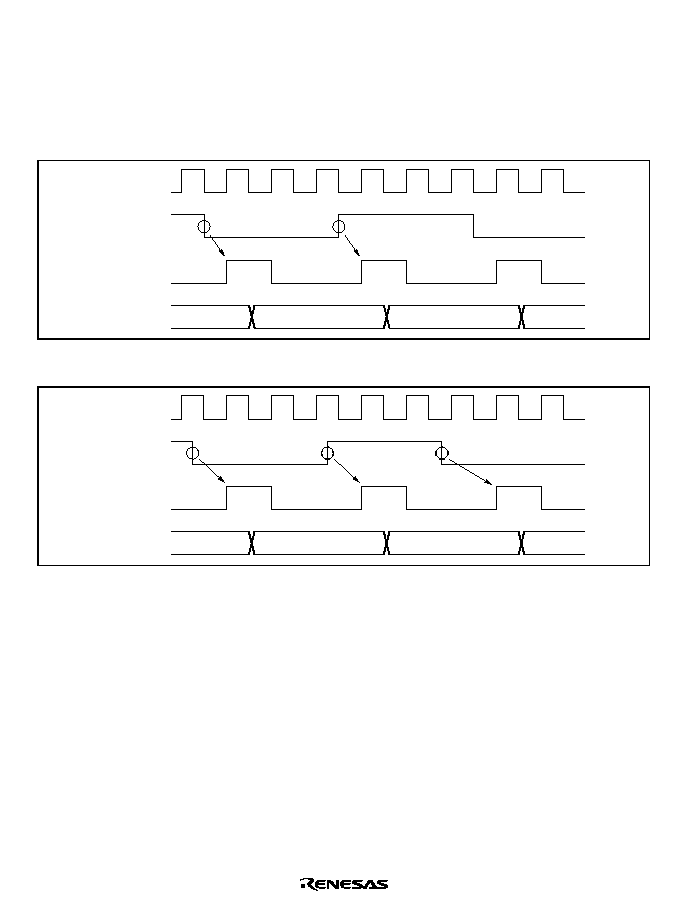
Rev. 2.0, 04/02, page 565 of 906
11.9
Operation Timing
11.9.1
Input/Output Timing
TCNT Count Timing: Figure 11.30 shows TCNT count timing in internal clock operation, and
figure 11.31 shows TCNT count timing in external clock operation.
TCNT
TCNT
input clock
Internal clock
N ≠ 1
N
N + 1
N + 2
Falling edge
Rising edge
Figure 11.30 Count Timing in Internal Clock Operation
TCNT
TCNT
input clock
External clock
N ≠ 1
N
N + 1
N + 2
Falling edge
Rising edge
Falling edge
Figure 11.31 Count Timing in External Clock Operation
Output Compare Output Timing: A compare match signal is generated in the final state in
which TCNT and TGR match (the point at which the count value matched by TCNT is updated).
When a compare match signal is generated, the output value set in TIOR is output at the output
compare output pin. After a match between TCNT and TGR, the compare match signal is not
generated until the (TIOC pin) TCNT input clock is generated.
Figure 11.32 shows output compare output timing.
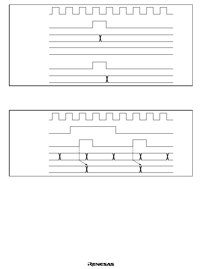
Rev. 2.0, 04/02, page 566 of 906
TGR
TCNT
TCNT
input clock
N
N
N + 1
Compare
match signal
TIOC pin
Figure 11.32 Output Compare Output Timing
Input Capture Signal Timing: Figure 11.33 shows input capture signal timing.
TCNT
Input capture
input
N
N + 1
N + 2
N
N + 2
TGR
Input capture
signal
Figure 11.33 Input Capture Input Signal Timing
Timing for Counter Clearing by Compare Match/Input Capture: Figure 11.34 shows the
timing when counter clearing by compare match occurrence is specified, and figure 11.35 shows
the timing when counter clearing by input capture occurrence is specified.

Rev. 2.0, 04/02, page 567 of 906
TCNT
Counter
clear signal
Compare
match signal
TGR
N
N
H'0000
Figure 11.34 Counter Clear Timing (Compare Match)
TCNT
Counter clear
signal
Input capture
signal
TGR
N
H'0000
N
Figure 11.35 Counter Clear Timing (Input Capture)
Buffer Operation Timing: Figures 11.36 and 11.37 show the timings in buffer operation.
TGRA,
TGRB
Compare
match signal
TCNT
TGRC,
TGRD
n
N
N
n
n + 1
Figure 11.36 Buffer Operation Timing (Compare Match)
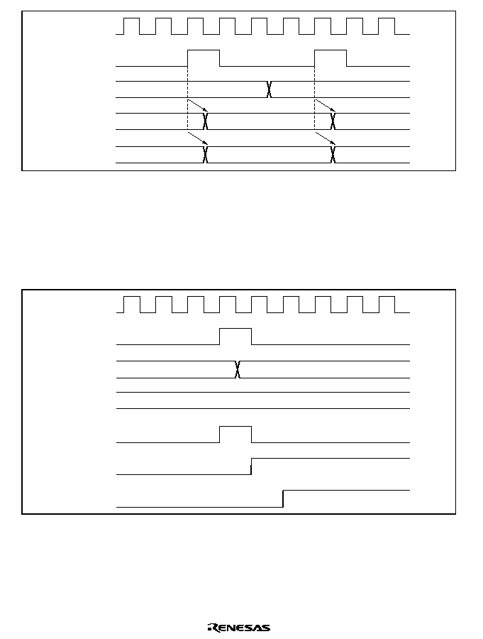
Rev. 2.0, 04/02, page 568 of 906
TGRA,
TGRB
TCNT
Input capture
signal
TGRC,
TGRD
N
n
n
N + 1
N
N
N + 1
Figure 11.37 Buffer Operation Timing (Input Capture)
11.9.2
Interrupt Signal Timing
TGF Flag Setting Timing in Case of Compare Match: Figure 11.38 shows the timing for
setting of the TGF flag in TSR by compare match occurrence, and the TGI interrupt request signal
timing.
TGR
TCNT
TCNT input
clock
N
N
N + 1
Compare
match signal
TGF flag
TGI interrupt
Figure 11.38 TGI Interrupt Timing (Compare Match)
TGF Flag Setting Timing in Case of Input Capture: Figure 11.39 shows the timing for setting
of the TGF flag in TSR by input capture occurrence, and the TGI interrupt request signal timing.
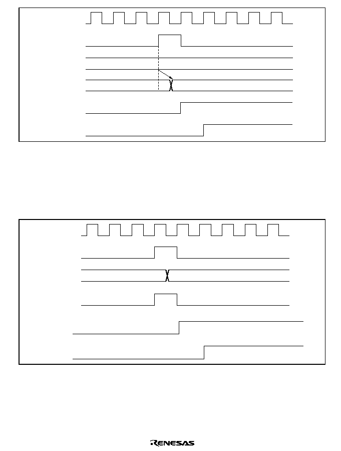
Rev. 2.0, 04/02, page 569 of 906
TGR
TCNT
Input capture
signal
N
N
TGF flag
TGI interrupt
Figure 11.39 TGI Interrupt Timing (Input Capture)
TCFV Flag/TCFU Flag Setting Timing: Figure 11.40 shows the timing for setting of the TCFV
flag in TSR by overflow occurrence, and the TCIV interrupt request signal timing.
Figure 11.41 shows the timing for setting of the TCFU flag in TSR by underflow occurrence, and
the TCIU interrupt request signal timing.
Overflow
signal
TCNT
(overflow)
TCNT input
clock
H'FFFF
H'0000
TCFV flag
TCIV interrupt
Figure 11.40 TCIV Interrupt Setting Timing
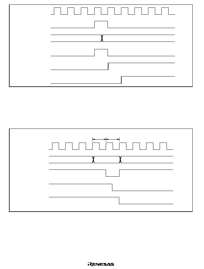
Rev. 2.0, 04/02, page 570 of 906
Underflow
signal
TCNT
(underflow)
TCNT
input clock
H'0000
H'FFFF
TCFU flag
TCIU interrupt
Figure 11.41 TCIU Interrupt Setting Timing
Status Flag Clearing Timing: After a status flag is read as 1 by the CPU, it is cleared by writing
0 to it. When the DTC or DMAC is activated, the flag is cleared automatically. Figure 11.42
shows the timing for status flag clearing by the CPU, and figure 11.43 shows the timing for status
flag clearing by the DTC or DMAC.
Status flag
Write signal
Address
TSR address
Interrupt
request
signal
TSR write cycle
T1
T2
Figure 11.42 Timing for Status Flag Clearing by CPU
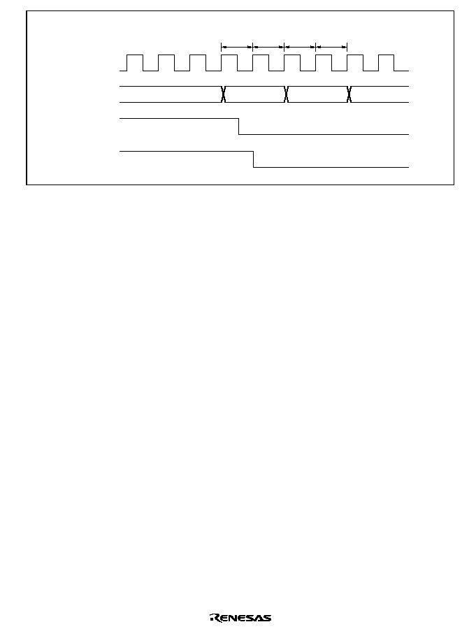
Rev. 2.0, 04/02, page 571 of 906
Interrupt
request
signal
Status flag
Address
Source address
DTC/DMAC
read cycle
T1
T2
Destination
address
T1
T2
DTC/DMAC
write cycle
Figure 11.43 Timing for Status Flag Clearing by DTC/DMAC Activation
11.10
Usage Notes
11.10.1
Module Stop Mode Setting
TPU operation can be disabled or enabled using the module stop control register. The initial
setting is for TPU operation to be halted. Register access is enabled by clearing module stop
mode. For details, refer to section 22, Power-Down Modes.
11.10.2
Input Clock Restrictions
The input clock pulse width must be at least 1.5 states in the case of single-edge detection, and at
least 2.5 states in the case of both-edge detection. The TPU will not operate properly with a
narrower pulse width.
In phase counting mode, the phase difference and overlap between the two input clocks must be at
least 1.5 states, and the pulse width must be at least 2.5 states. Figure 11.44 shows the input clock
conditions in phase counting mode.
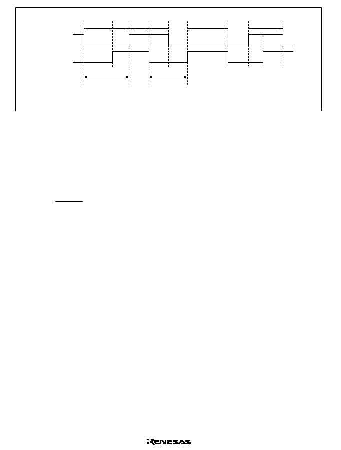
Rev. 2.0, 04/02, page 572 of 906
Overlap
Phase
diffe-
rence
Phase
diffe-
rence
Overlap
TCLKA
(TCLKC)
TCLKB
(TCLKD)
Pulse width
Pulse width
Pulse width
Pulse width
Notes: Phase difference and overlap
Pulse width
: 1.5 states or more
: 2.5 states or more
Figure 11.44 Phase Difference, Overlap, and Pulse Width in Phase Counting Mode
11.10.3
Caution on Cycle Setting
When counter clearing by compare match is set, TCNT is cleared in the final state in which it
matches the TGR value (the point at which the count value matched by TCNT is updated).
Consequently, the actual counter frequency is given by the following formula:
f =
¯
(N + 1)
Where
f: Counter frequency
¯: Operating frequency
N: TGR set value
11.10.4
Contention between TCNT Write and Clear Operations
If the counter clearing signal is generated in the T2 state of a TCNT write cycle, TCNT clearing
takes precedence and the TCNT write is not performed. Figure 11.45 shows the timing in this
case.

Rev. 2.0, 04/02, page 573 of 906
Counter clearing
signal
Write signal
Address
¯
TCNT address
TCNT
TCNT write cycle
T1
T2
N
H'0000
Figure 11.45 Contention between TCNT Write and Clear Operations
11.10.5
Contention between TCNT Write and Increment Operations
If incrementing occurs in the T2 state of a TCNT write cycle, the TCNT write takes precedence
and TCNT is not incremented. Figure 11.46 shows the timing in this case.
TCNT input
clock
Write signal
Address
¯
TCNT address
TCNT
TCNT write cycle
T1
T2
N
M
TCNT write data
Figure 11.46 Contention between TCNT Write and Increment Operations
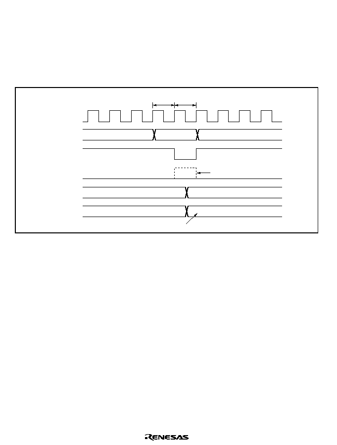
Rev. 2.0, 04/02, page 574 of 906
11.10.6
Contention between TGR Write and Compare Match
If a compare match occurs in the T2 state of a TGR write cycle, the TGR write takes precedence
and the compare match signal is disabled. A compare match also does not occur when the same
value as before is written.
Figure 11.47 shows the timing in this case.
Compare
match signal
Write signal
Address
¯
TGR address
TCNT
TGR write cycle
T1
T2
N
M
TGR write data
TGR
N
N + 1
Disabled
Figure 11.47 Contention between TGR Write and Compare Match
11.10.7
Contention between Buffer Register Write and Compare Match
If a compare match occurs in the T2 state of a TGR write cycle, the data transferred to TGR by the
buffer operation will be the data prior to the write.
Figure 11.48 shows the timing in this case.
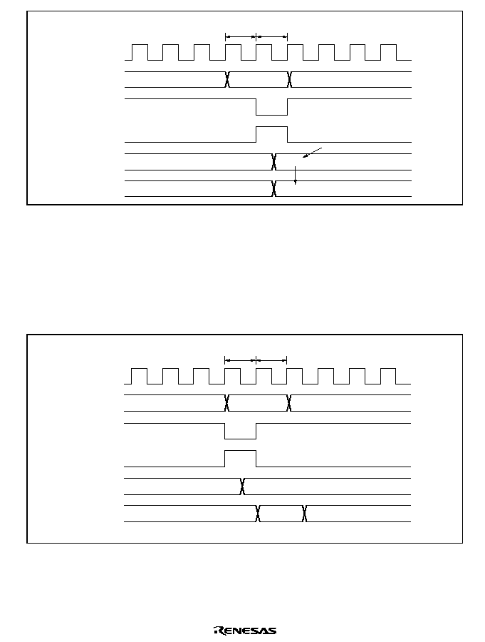
Rev. 2.0, 04/02, page 575 of 906
Compare
match signal
Write signal
Address
¯
Buffer register
address
Buffer
register
TGR write cycle
T1
T2
N
TGR
N
M
Buffer register write data
Figure 11.48 Contention between Buffer Register Write and Compare Match
11.10.8
Contention between TGR Read and Input Capture
If the input capture signal is generated in the T1 state of a TGR read cycle, the data that is read
will be the data after input capture transfer.
Figure 11.49 shows the timing in this case.
Input capture
signal
Read signal
Address
¯
TGR address
TGR
TGR read cycle
T1
T2
M
Internal
data bus
X
M
Figure 11.49 Contention between TGR Read and Input Capture
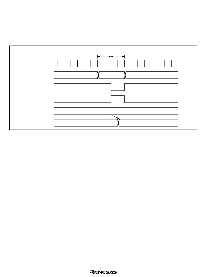
Rev. 2.0, 04/02, page 576 of 906
11.10.9
Contention between TGR Write and Input Capture
If the input capture signal is generated in the T2 state of a TGR write cycle, the input capture
operation takes precedence and the write to TGR is not performed.
Figure 11.50 shows the timing in this case.
Input capture
signal
Write signal
Address
¯
TCNT
TGR write cycle
T1
T2
M
TGR
M
TGR address
Figure 11.50 Contention between TGR Write and Input Capture
11.10.10 Contention between Buffer Register Write and Input Capture
If the input capture signal is generated in the T2 state of a buffer register write cycle, the buffer
operation takes precedence and the write to the buffer register is not performed.
Figure 11.51 shows the timing in this case.
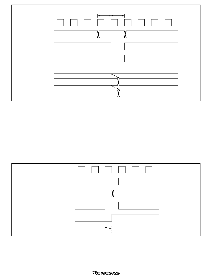
Rev. 2.0, 04/02, page 577 of 906
Input capture
signal
Write signal
Address
¯
TCNT
Buffer register write cycle
T1
T2
N
TGR
N
M
M
Buffer
register
Buffer register
address
Figure 11.51 Contention between Buffer Register Write and Input Capture
11.10.11 Contention between Overflow/Underflow and Counter Clearing
If overflow/underflow and counter clearing occur simultaneously, the TCFV/TCFU flag in TSR is
not set and TCNT clearing takes precedence.
Figure 11.52 shows the operation timing when a TGR compare match is specified as the clearing
source, and H'FFFF is set in TGR.
Counter
clearing signal
TCNT input
clock
¯
TCNT
TGF
Disabled
TCFV
H'FFFF
H'0000
Figure 11.52 Contention between Overflow and Counter Clearing
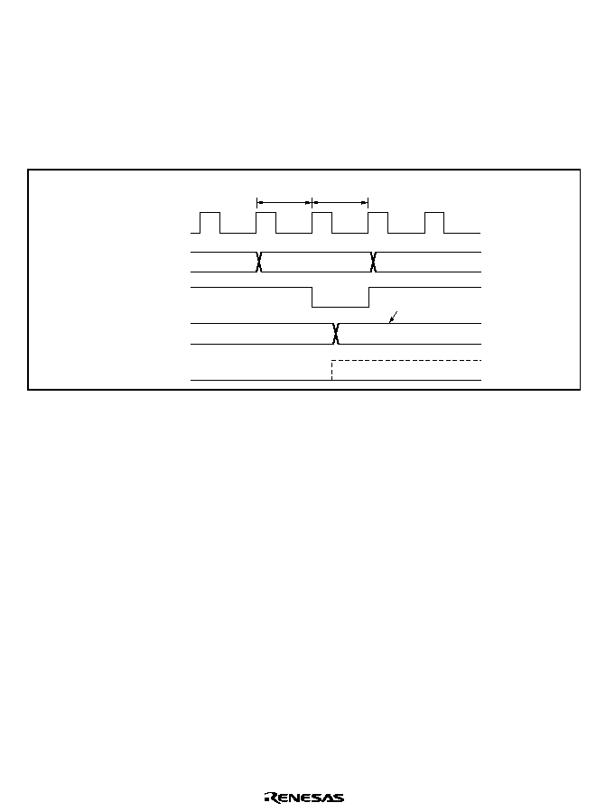
Rev. 2.0, 04/02, page 578 of 906
11.10.12 Contention between TCNT Write and Overflow/Underflow
If there is an up-count or down-count in the T2 state of a TCNT write cycle, when
overflow/underflow occurs, the TCNT write takes precedence and the TCFV/TCFU flag in TSR is
not set.
Figure 11.53 shows the operation timing when there is contention between TCNT write and
overflow.
Write signal
Address
¯
TCNT address
TCNT
TCNT write cycle
T1
T2
H'FFFF
M
TCNT write data
TCFV flag
Figure 11.53 Contention between TCNT Write and Overflow
11.10.13 Multiplexing of I/O Pins
In this LSI, the TCLKA input pin is multiplexed with the TIOCC0 I/O pin, the TCLKB input pin
with the TIOCD0 I/O pin, the TCLKC input pin with the TIOCB1 I/O pin, and the TCLKD input
pin with the TIOCB2 I/O pin. When an external clock is input, compare match output should not
be performed from a multiplexed pin.
11.10.14 Interrupts and Module Stop Mode
If module stop mode is entered when an interrupt has been requested, it will not be possible to
clear the CPU interrupt source or the DMAC or DTC activation source. Interrupts should therefore
be disabled before entering module stop mode.

Rev. 2.0, 04/02, page 579 of 906
Section 12 Programmable Pulse Generator (PPG)
The programmable pulse generator (PPG) provides pulse outputs by using the 16-bit timer pulse
unit (TPU) as a time base. The PPG pulse outputs are divided into 4-bit groups (groups 3 to 0) that
can operate both simultaneously and independently. The block diagram of PPG is shown in figure
12.1
12.1
Features
∑
16-bit output data
∑
Four output groups
∑
Selectable output trigger signals
∑
Non-overlap mode
∑
Can operate together with the data transfer controller (DTC) and the DMA controller (DMAC)
∑
Settable inverted output
∑
Module stop mode can be set
PPG0001A_000020020400
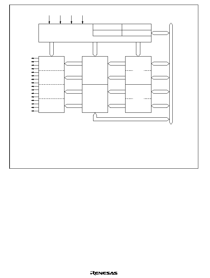
Rev. 2.0, 04/02, page 580 of 906
Compare match signals
PO15
PO14
PO13
PO12
PO11
PO10
PO9
PO8
PO7
PO6
PO5
PO4
PO3
PO2
PO1
PO0
Legend
PMR
PCR
NDERH
NDERL
NDRH
NDRL
PODRH
PODRL
: PPG output mode register
: PPG output control register
: Next data enable register H
: Next data enable register L
: Next data register H
: Next data register L
: Output data register H
: Output data register L
Internal
data bus
Pulse output
pins, group 3
Pulse output
pins, group 2
Pulse output
pins, group 1
Pulse output
pins, group 0
PODRH
PODRL
NDRH
NDRL
Control logic
NDERH
PMR
NDERL
PCR
Figure 12.1 Block Diagram of PPG

Rev. 2.0, 04/02, page 581 of 906
12.2
Input/Output Pins
Table 12.1 shows the PPG pin configuration.
Table 12.1
Pin Configuration
Pin Name
I/O
Function
PO15
Output
PO14
Output
PO13
Output
PO12
Output
Group 3 pulse output
PO11
Output
PO10
Output
PO9
Output
PO8
Output
Group 2 pulse output
PO7
Output
PO6
Output
PO5
Output
PO4
Output
Group 1 pulse output
PO3
Output
PO2
Output
PO1
Output
PO0
Output
Group 0 pulse output
12.3
Register Descriptions
The PPG has the following registers.
∑
Next data enable register H (NDERH)
∑
Next data enable register L (NDERL)
∑
Output data register H (PODRH)
∑
Output data register L (PODRL)
∑
Next data register H (NDRH)
∑
Next data register L (NDRL)
∑
PPG output control register (PCR)
∑
PPG output mode register (PMR)

Rev. 2.0, 04/02, page 582 of 906
12.3.1
Next Data Enable Registers H, L (NDERH, NDERL)
NDERH, NDERL enable or disable pulse output on a bit-by-bit basis. For outputting pulse by the
PPG, set the corresponding DDR to 1.
NDERH
Bit
Bit Name
Initial Value
R/W
Description
7
6
5
4
3
2
1
0
NDER15
NDER14
NDER13
NDER12
NDER11
NDER10
NDER9
NDER8
0
0
0
0
0
0
0
0
R/W
R/W
R/W
R/W
R/W
R/W
R/W
R/W
Next Data Enable 15 to 8
When a bit is set to 1, the value in the
corresponding NDRH bit is transferred to the
PODRH bit by the selected output trigger. Values
are not transferred from NDRH to PODRH for
cleared bits.
NDERL
Bit
Bit Name
Initial Value
R/W
Description
7
6
5
4
3
2
1
0
NDER7
NDER6
NDER5
NDER4
NDER3
NDER2
NDER1
NDER0
0
0
0
0
0
0
0
0
R/W
R/W
R/W
R/W
R/W
R/W
R/W
R/W
Next Data Enable 7 to 0
When a bit is set to 1, the value in the
corresponding NDRL bit is transferred to the
PODRL bit by the selected output trigger. Values
are not transferred from NDRL to PODRL for
cleared bits.

Rev. 2.0, 04/02, page 583 of 906
12.3.2
Output Data Registers H, L (PODRH, PODRL)
PODRH and PODRL store output data for use in pulse output. A bit that has been set for pulse
output by NDER is read-only and cannot be modified.
PODRH
Bit
Bit Name
Initial Value
R/W
Description
7
6
5
4
3
2
1
0
POD15
POD14
POD13
POD12
POD11
POD10
POD9
POD8
0
0
0
0
0
0
0
0
R/W
R/W
R/W
R/W
R/W
R/W
R/W
R/W
Output Data Register 15 to 8
For bits which have been set to pulse output by
NDERH, the output trigger transfers NDRH values
to this register during PPG operation. While
NDERH is set to 1, the CPU cannot write to this
register. While NDERH is cleared, the initial output
value of the pulse can be set.
PODRL
Bit
Bit Name
Initial Value
R/W
Description
7
6
5
4
3
2
1
0
POD7
POD6
POD5
POD4
POD3
POD2
POD1
POD0
0
0
0
0
0
0
0
0
R/W
R/W
R/W
R/W
R/W
R/W
R/W
R/W
Output Data Register 7 to 0
For bits which have been set to pulse output by
NDERL, the output trigger transfers NDRL values
to this register during PPG operation. While
NDERL is set to 1, the CPU cannot write to this
register. While NDERL is cleared, the initial output
value of the pulse can be set.

Rev. 2.0, 04/02, page 584 of 906
12.3.3
Next Data Registers H, L (NDRH, NDRL)
NDRH, NDRL store the next data for pulse output. The NDR addresses differ depending on
whether pulse output groups have the same output trigger or different output triggers.
NDRH
If pulse output groups 2 and 3 have the same output trigger, all eight bits are mapped to the same
address and can be accessed at one time, as shown below.
Bit
Bit Name
Initial Value
R/W
Description
7
6
5
4
3
2
1
0
NDR15
NDR14
NDR13
NDR12
NDR11
NDR10
NDR9
NDR8
0
0
0
0
0
0
0
0
R/W
R/W
R/W
R/W
R/W
R/W
R/W
R/W
Next Data Register 15 to 8
The register contents are transferred to the
corresponding PODRH bits by the output trigger
specified with PCR.
If pulse output groups 2 and 3 have different output triggers, upper 4 bits and lower 4 bits are
mapped to the different addresses as shown below.
Bit
Bit Name
Initial Value
R/W
Description
7
6
5
4
NDR15
NDR14
NDR13
NDR12
0
0
0
0
R/W
R/W
R/W
R/W
Next Data Register 15 to 12
The register contents are transferred to the
corresponding PODRH bits by the output trigger
specified with PCR.
3
to
0
--
All 1
--
Reserved
These bits are always read as 1 and cannot be
modified.

Rev. 2.0, 04/02, page 585 of 906
Bit
Bit Name
Initial Value
R/W
Description
7
to
4
--
All 1
--
Reserved
These bits are always read as 1 and cannot be
modified.
3
2
1
0
NDR11
NDR10
NDR9
NDR8
0
0
0
0
R/W
R/W
R/W
R/W
Next Data Register 11 to 8
The register contents are transferred to the
corresponding PODRH bits by the output trigger
specified with PCR.
NDRL
If pulse output groups 0 and 1 have the same output trigger, all eight bits are mapped to the same
address and can be accessed at one time, as shown below.
Bit
Bit Name
Initial Value
R/W
Description
7
6
5
4
3
2
1
0
NDR7
NDR6
NDR5
NDR4
NDR3
NDR2
NDR1
NDR0
0
0
0
0
0
0
0
0
R/W
R/W
R/W
R/W
R/W
R/W
R/W
R/W
Next Data Register 7 to 0
The register contents are transferred to the
corresponding PODRL bits by the output trigger
specified with PCR.
If pulse output groups 0 and 1 have different output triggers, upper 4 bits and lower 4 bits are
mapped to the different addresses as shown below.
Bit
Bit Name
Initial Value
R/W
Description
7
6
5
4
NDR7
NDR6
NDR5
NDR4
0
0
0
0
R/W
R/W
R/W
R/W
Next Data Register 7 to 4
The register contents are transferred to the
corresponding PODRL bits by the output trigger
specified with PCR.
3
to
0
--
All 1
--
Reserved
These bits are always read as 1 and cannot be
modified.

Rev. 2.0, 04/02, page 586 of 906
Bit
Bit Name
Initial Value
R/W
Description
7
to
4
--
All 1
--
Reserved
These bits are always read as 1 and cannot be
modified.
3
2
1
0
NDR3
NDR2
NDR1
NDR0
0
0
0
0
R/W
R/W
R/W
R/W
Next Data Register 3 to 0
The register contents are transferred to the
corresponding PODRL bits by the output trigger
specified with PCR.
12.3.4
PPG Output Control Register (PCR)
PCR selects output trigger signals on a group-by-group basis. For details on output trigger
selection, refer to section 12.3.5, PPG Output Mode Register (PMR).
Bit
Bit Name
Initial Value
R/W
Description
7
6
G3CMS1
G3CMS0
1
1
R/W
R/W
Group 3 Compare Match Select 1 and 0
Select output trigger of pulse output group 3.
00: Compare match in TPU channel 0
01: Compare match in TPU channel 1
10: Compare match in TPU channel 2
11: Compare match in TPU channel 3
5
4
G2CMS1
G2CMS0
1
1
R/W
R/W
Group 2 Compare Match Select 1 and 0
Select output trigger of pulse output group 2.
00: Compare match in TPU channel 0
01: Compare match in TPU channel 1
10: Compare match in TPU channel 2
11: Compare match in TPU channel 3
3
2
G1CMS1
G1CMS0
1
1
R/W
R/W
Group 1 Compare Match Select 1 and 0
Select output trigger of pulse output group 1.
00: Compare match in TPU channel 0
01: Compare match in TPU channel 1
10: Compare match in TPU channel 2
11: Compare match in TPU channel 3

Rev. 2.0, 04/02, page 587 of 906
Bit
Bit Name
Initial Value
R/W
Description
1
0
G0CMS1
G0CMS0
1
1
R/W
R/W
Group 0 Compare Match Select 1 and 0
Select output trigger of pulse output group 0.
00: Compare match in TPU channel 0
01: Compare match in TPU channel 1
10: Compare match in TPU channel 2
11: Compare match in TPU channel 3
12.3.5
PPG Output Mode Register (PMR)
PMR selects the pulse output mode of the PPG for each group. If inverted output is selected, a
low-level pulse is output when PODRH is 1 and a high-level pulse is output when PODRH is 0. If
non-overlapping operation is selected, PPG updates its output values at compare match A or B of
the TPU that becomes the output trigger. For details, refer to section 12.4.4, Non-Overlapping
Pulse Output.
Bit
Bit Name
Initial Value
R/W
Description
7
G3INV
1
R/W
Group 3 Inversion
Selects direct output or inverted output for pulse
output group 3.
0: Inverted output
1: Direct output
6
G2INV
1
R/W
Group 2 Inversion
Selects direct output or inverted output for pulse
output group 2.
0: Inverted output
1: Direct output
5
G1INV
1
R/W
Group 1 Inversion
Selects direct output or inverted output for pulse
output group 1.
0: Inverted output
1: Direct output
4
G0INV
1
R/W
Group 0 Inversion
Selects direct output or inverted output for pulse
output group 0.
0: Inverted output
1: Direct output

Rev. 2.0, 04/02, page 588 of 906
Bit
Bit Name
Initial Value
R/W
Description
3
G3NOV
0
R/W
Group 3 Non-Overlap
Selects normal or non-overlapping operation for
pulse output group 3.
0: Normal operation (output values updated at
compare match A in the selected TPU channel)
1: Non-overlapping operation (output values
updated at compare match A or B in the selected
TPU channel)
2
G2NOV
0
R/W
Group 2 Non-Overlap
Selects normal or non-overlapping operation for
pulse output group 2.
0: Normal operation (output values updated at
compare match A in the selected TPU channel)
1: Non-overlapping operation (output values
updated at compare match A or B in the selected
TPU channel)
1
G1NOV
0
R/W
Group 1 Non-Overlap
Selects normal or non-overlapping operation for
pulse output group 1.
0: Normal operation (output values updated at
compare match A in the selected TPU channel)
1: Non-overlapping operation (output values
updated at compare match A or B in the selected
TPU channel)
0
G0NOV
0
R/W
Group 0 Non-Overlap
Selects normal or non-overlapping operation for
pulse output group 0.
0: Normal operation (output values updated at
compare match A in the selected TPU channel)
1: Non-overlapping operation (output values
updated at compare match A or B in the selected
TPU channel)
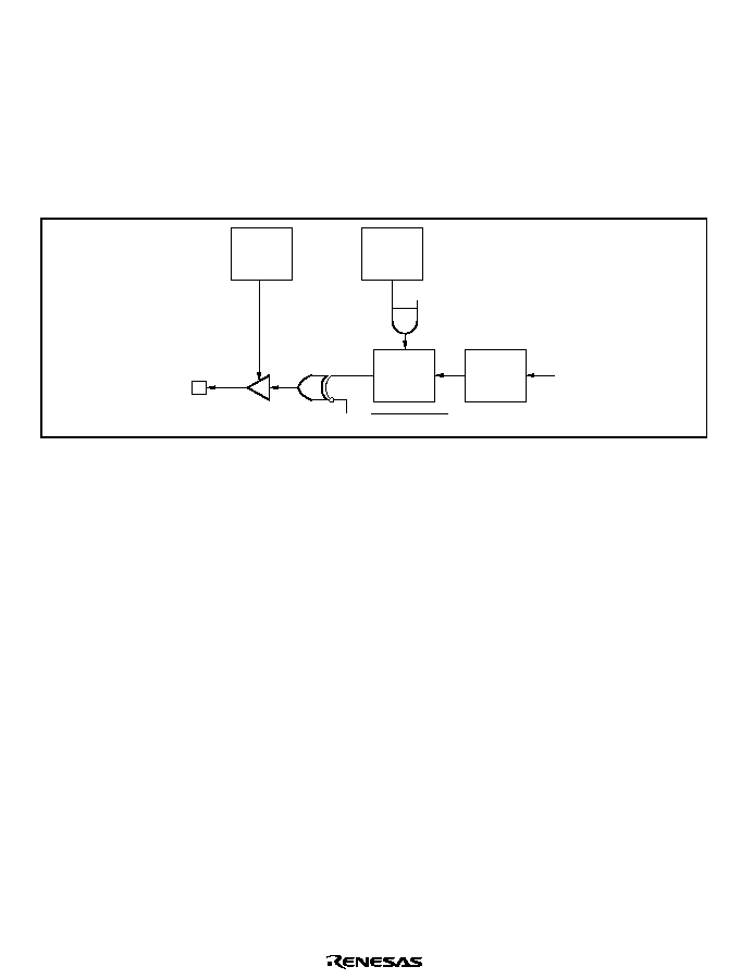
Rev. 2.0, 04/02, page 589 of 906
12.4
Operation
Figure 12.2 shows an overview diagram of the PPG. PPG pulse output is enabled when the
corresponding bits in P1DDR, P2DDR, and NDER are set to 1. An initial output value is
determined by its corresponding PODR initial setting. When the compare match event specified
by PCR occurs, the corresponding NDR bit contents are transferred to PODR to update the output
values. Sequential output of data of up to 16 bits is possible by writing new output data to NDR
before the next compare match.
Output trigger signal
Pulse output pin
Internal data bus
Normal output/inverted output
C
PODR
Q
D
NDER
Q
NDR
Q
D
DDR
Figure 12.2 Overview Diagram of PPG
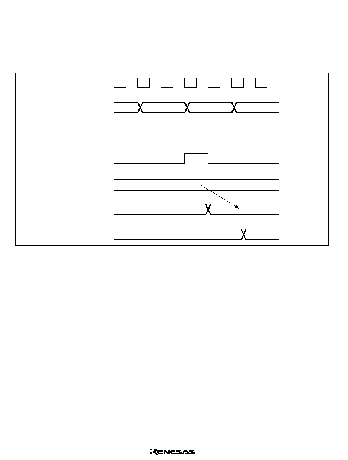
Rev. 2.0, 04/02, page 590 of 906
12.4.1
Output Timing
If pulse output is enabled, NDR contents are transferred to PODR and output when the specified
compare match event occurs. Figure 12.3 shows the timing of these operations for the case of
normal output in groups 2 and 3, triggered by compare match A.
TCNT
N
N + 1
¯
TGRA
N
Compare match
A signal
NDRH
m
n
PODRH
PO8 to PO15
n
m
n
Figure 12.3 Timing of Transfer and Output of NDR Contents (Example)
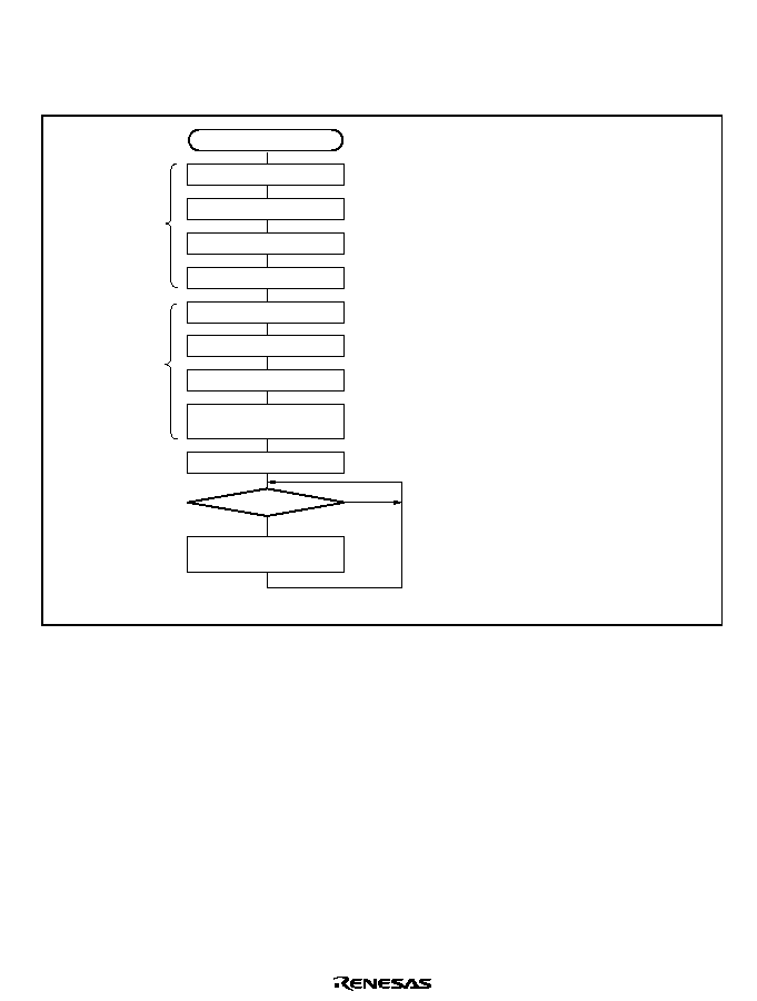
Rev. 2.0, 04/02, page 591 of 906
12.4.2
Sample Setup Procedure for Normal Pulse Output
Figure 12.4 shows a sample procedure for setting up normal pulse output.
Select TGR functions
[1]
Set TGRA value
Set counting operation
Select interrupt request
Set initial output data
Enable pulse output
Select output trigger
Set next pulse
output data
Start counter
Set next pulse
output data
Normal PPG output
No
Yes
TPU setup
Port and
PPG setup
TPU setup
[2]
[3]
[4]
[5]
[6]
[7]
[8]
[9]
[10]
Compare match?
[1] Set TIOR to make TGRA an output
compare register (with output
disabled)
[2] Set the PPG output trigger period
[3] Select the counter clock source with
bits TPSC2 to TPSC0 in TCR.
Select the counter clear source with
bits CCLR2 to CCLR0.
[4] Enable the TGIA interrupt in TIER.
The DTC or DMAC can also be set
up to transfer data to NDR.
[5] Set the initial output values in
PODR.
[6] Set the DDR and NDER bits for the
pins to be used for pulse output to 1.
[7] Select the TPU compare match
event to be used as the output
trigger in PCR.
[8] Set the next pulse output values in
NDR.
[9] Set the CST bit in TSTR to 1 to start
the TCNT counter.
[10] At each TGIA interrupt, set the next
output values in NDR.
Figure 12.4 Setup Procedure for Normal Pulse Output (Example)
Rev. 2.0, 04/02, page 592 of 906
12.4.3
Example of Normal Pulse Output (Example of Five-Phase Pulse Output)
Figure 12.5 shows an example in which pulse output is used for cyclic five-phase pulse output.
TCNT value
TCNT
TGRA
H'0000
NDRH
00
80
C0
40
60
20
30
10
18
08
88
PODRH
PO15
PO14
PO13
PO12
PO11
Time
Compare match
C0
80
C0
80
40
60
20
30
10
18
08
88
80
C0
40
Figure 12.5 Normal Pulse Output Example (Five-Phase Pulse Output)
1. Set up TGRA in TPU which is used as the output trigger to be an output compare register. Set
a cycle in TGRA so the counter will be cleared by compare match A. Set the TGIEA bit in
TIER to 1 to enable the compare match/input capture A (TGIA) interrupt.
2. Write H'F8 in P1DDR and NDERH, and set the G3CMS1, G3CMS0, G2CMS1, and G2CMS0
bits in PCR to select compare match in the TPU channel set up in the previous step to be the
output trigger. Write output data H'80 in NDRH.
3. The timer counter in the TPU channel starts. When compare match A occurs, the NDRH
contents are transferred to PODRH and output. The TGIA interrupt handling routine writes the
next output data (H'C0) in NDRH.
4. Five-phase pulse output (one or two phases active at a time) can be obtained subsequently by
writing H'40, H'60, H'20, H'30, H'10, H'18, H'08, H'88... at successive TGIA interrupts.
If the DTC or DMAC is set for activation by the TGIA interrupt, pulse output can be obtained
without imposing a load on the CPU.
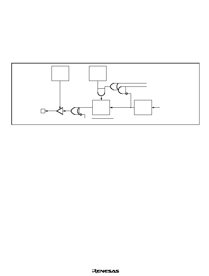
Rev. 2.0, 04/02, page 593 of 906
12.4.4
Non-Overlapping Pulse Output
During non-overlapping operation, transfer from NDR to PODR is performed as follows:
∑
NDR bits are always transferred to PODR bits at compare match A.
∑
At compare match B, NDR bits are transferred only if their value is 0. Bits are not transferred
if their value is 1.
Figure 12.6 illustrates the non-overlapping pulse output operation.
Compare match A
Compare match B
Pulse
output
pin
Internal data bus
Normal output/inverted output
C
PODR
Q
D
NDER
Q
NDR
Q
D
DDR
Figure 12.6 Non-Overlapping Pulse Output
Therefore, 0 data can be transferred ahead of 1 data by making compare match B occur before
compare match A.
The NDR contents should not be altered during the interval from compare match B to compare
match A (the non-overlap margin).
This can be accomplished by having the TGIA interrupt handling routine write the next data in
NDR, or by having the TGIA interrupt activate the DTC or DMAC. Note, however, that the next
data must be written before the next compare match B occurs.
Figure 12.7 shows the timing of this operation.
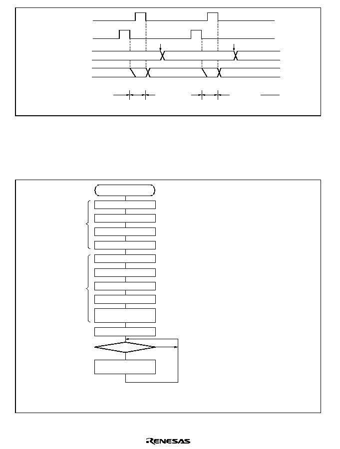
Rev. 2.0, 04/02, page 594 of 906
0/1 output
0 output
0/1 output
0 output
Do not write
to NDR here
Write to NDR
here
Compare match A
Compare match B
NDR
PODR
Do not write
to NDR here
Write to NDR
here
Write to NDR
Write to NDR
Figure 12.7 Non-Overlapping Operation and NDR Write Timing
12.4.5
Sample Setup Procedure for Non-Overlapping Pulse Output
Figure 12.8 shows a sample procedure for setting up non-overlapping pulse output.
Select TGR functions
[1]
Set TGR values
Set counting operation
Select interrupt request
Set initial output data
Enable pulse output
Select output trigger
Set next pulse
output data
Start counter
Set next pulse
output data
Compare match A?
No
Yes
TPU setup
PPG setup
TPU setup
Non-overlapping
pulse output
Set non-overlapping groups
[2]
[3]
[4]
[5]
[6]
[7]
[8]
[9]
[10]
[11]
[1] Set TIOR to make TGRA and
TGRB an output compare registers
(with output disabled)
[2] Set the pulse output trigger period
in TGRB and the non-overlap
period in TGRA.
[3] Select the counter clock source
with bits TPSC2 to TPSC0 in TCR.
Select the counter clear source
with bits CCLR2 to CCLR0.
[4] Enable the TGIA interrupt in TIER.
The DTC or DMAC can also be set
up to transfer data to NDR.
[5] Set the initial output values in
PODR.
[6] Set the DDR and NDER bits for the
pins to be used for pulse output to
1.
[7] Select the TPU compare match
event to be used as the pulse
output trigger in PCR.
[8] In PMR, select the groups that will
operate in non-overlap mode.
[9] Set the next pulse output values in
NDR.
[10] Set the CST bit in TSTR to 1 to
start the TCNT counter.
[11] At each TGIA interrupt, set the next
output values in NDR.
Figure 12.8 Setup Procedure for Non-Overlapping Pulse Output (Example)

Rev. 2.0, 04/02, page 595 of 906
12.4.6
Example of Non-Overlapping Pulse Output (Example of Four-Phase
Complementary Non-Overlapping Output)
Figure 12.9 shows an example in which pulse output is used for four-phase complementary non-
overlapping pulse output.
TCNT value
TCNT
TGRB
TGRA
H'0000
NDRH
95
65
59
56
95
65
00
95
05
65
41
59
50
56
14
95
05
65
PODRH
PO15
PO14
PO13
PO12
PO11
PO10
PO9
PO8
Time
Non-overlap margin
Figure 12.9 Non-Overlapping Pulse Output Example (Four-Phase Complementary)
1. Set up the TPU channel to be used as the output trigger channel so that TGRA and TGRB are
output compare registers. Set the trigger period in TGRB and the non-overlap margin in
TGRA, and set the counter to be cleared by compare match B. Set the TGIEA bit in TIER to 1
to enable the TGIA interrupt.
2. Write H'FF in P1DDR and NDERH, and set the G3CMS1, G3CMS0, G2CMS1, and G2CMS0
bits in PCR to select compare match in the TPU channel set up in the previous step to be the
output trigger. Set the G3NOV and G2NOV bits in PMR to 1 to select non-overlapping output.
Write output data H'95 in NDRH.
3. The timer counter in the TPU channel starts. When a compare match with TGRB occurs,
outputs change from 1 to 0. When a compare match with TGRA occurs, outputs change from 0

Rev. 2.0, 04/02, page 596 of 906
to 1 (the change from 0 to 1 is delayed by the value set in TGRA). The TGIA interrupt
handling routine writes the next output data (H'65) in NDRH.
4. Four-phase complementary non-overlapping pulse output can be obtained subsequently by
writing H'59, H'56, H'95... at successive TGIA interrupts.
If the DTC or DMAC is set for activation by the TGIA interrupt, pulse output can be obtained
without imposing a load on the CPU.
12.4.7
Inverted Pulse Output
If the G3INV, G2INV, G1INV, and G0INV bits in PMR are cleared to 0, values that are the
inverse of the PODR contents can be output.
Figure 12.10 shows the outputs when G3INV and G2INV are cleared to 0, in addition to the
settings of figure 12.9.
TCNT value
TCNT
TGRB
TGRA
H'0000
NDRH
95
65
59
56
95
65
00
95
05
65
41
59
50
56
14
95
05
65
PODRL
PO15
PO14
PO13
PO12
PO11
PO10
PO9
PO8
Time
Figure 12.10 Inverted Pulse Output (Example)
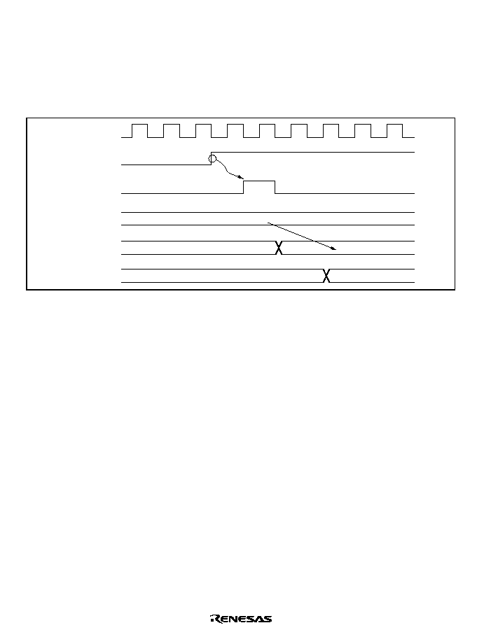
Rev. 2.0, 04/02, page 597 of 906
12.4.8
Pulse Output Triggered by Input Capture
Pulse output can be triggered by TPU input capture as well as by compare match. If TGRA
functions as an input capture register in the TPU channel selected by PCR, pulse output will be
triggered by the input capture signal.
Figure 12.11 shows the timing of this output.
¯
N
M
N
TIOC pin
Input capture
signal
NDR
PODR
M
N
PO
Figure 12.11 Pulse Output Triggered by Input Capture (Example)
12.5
Usage Notes
12.5.1
Module Stop Mode Setting
PPG operation can be disabled or enabled using the module stop control register. The initial value
is for PPG operation to be halted. Register access is enabled by clearing module stop mode. For
details, refer to section 22, Power-Down Modes.
12.5.2
Operation of Pulse Output Pins
Pins PO0 to PO15 are also used for other peripheral functions such as the TPU. When output by
another peripheral function is enabled, the corresponding pins cannot be used for pulse output.
Note, however, that data transfer from NDR bits to PODR bits takes place, regardless of the usage
of the pins.
Pin functions should be changed only under conditions in which the output trigger event will not
occur.

Rev. 2.0, 04/02, page 598 of 906

Rev. 2.0, 04/02, page 599 of 906
Section 13 8-Bit Timers (TMR)
This LSI has an on-chip 8-bit timer module with two channels operating on the basis of an 8-bit
counter. The 8-bit timer module can be used to count external events and be used as a
multifunction timer in a variety of applications, such as generation of counter reset, interrupt
requests, and pulse output with an arbitrary duty cycle using a compare-match signal with two
registers.
13.1
Features
∑
Selection of four clock sources
The counters can be driven by one of three internal clock signals (¯/8, ¯/64, or ¯/8192) or an
external clock input
∑
Selection of three ways to clear the counters
The counters can be cleared on compare match A or B, or by an external reset signal
∑
Timer output control by a combination of two compare match signals
The timer output signal in each channel is controlled by a combination of two independent
compare match signals, enabling the timer to generate output waveforms with an arbitrary duty
cycle or PWM output
∑
Provision for cascading of two channels (TMR_0 and TMR_1)
Operation as a 16-bit timer is possible, using TMR_0 for the upper 8 bits and TMR_1 for the
lower 8 bits (16-bit count mode)
TMR_1 can be used to count TMR_0 compare matches (compare match count mode)
∑
Three independent interrupts
Compare match A and B and overflow interrupts can be requested independently
∑
A/D converter conversion start trigger can be generated
TIMH260A_000020020400
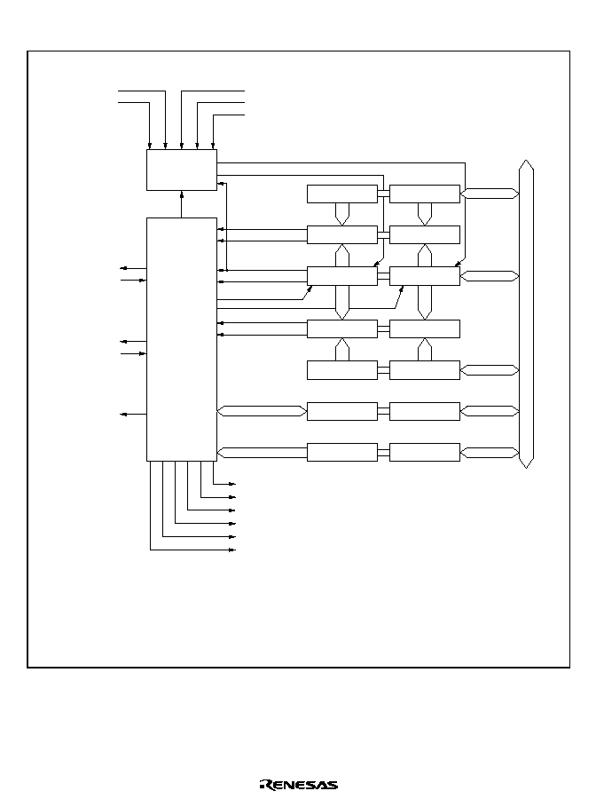
Rev. 2.0, 04/02, page 600 of 906
Figure 13.1 shows a block diagram of the 8-bit timer module (TMR_0 and TMR_1).
External clock source
Internal clock sources
TMR_0
ÿ
/8
ÿ
/64
ÿ
/8192
TMR_1
ÿ
/8
ÿ
/64
ÿ
/8192
Clock 1
Clock 0
Compare match A1
Compare match A0
Clear 1
CMIA0
CMIB0
OVI0
CMIA1
CMIB1
OVI1
Interrupt signals
TCORA_0 : Time constant register A_0
TCORB_0 : Time constant register B_0
TCNT_0
: Timer counter_0
TCSR_0
: Timer control/status register_0
TCR_0
: Timer control register_0
TCORA_1 : Time constant register A_1
TCORB_1 : Time constant register B_1
TCNT_1
: Timer counter_1
TCSR_1
: Timer control/status register_1
TCR_1
: Timer control register_1
TMO0
TMRI0
Internal bus
TCORA_0
Comparator A_0
Comparator B_0
TCORB_0
TCSR_0
TCR_0
TCORA_1
Comparator A_1
TCNT_1
Comparator B_1
TCORB_1
TCSR_1
TCR_1
TMCI0
TMCI1
TCNT_0
Overflow 1
Overflow 0
Compare match B1
Compare match B0
TMO1
TMRI1
A/D
conversion
start request
signal
Clock select
Control logic
Clear 0
Legend
Figure 13.1 Block Diagram of 8-Bit Timer Module

Rev. 2.0, 04/02, page 601 of 906
13.2
Input/Output Pins
Table 13.1 shows the pin configuration of the 8-bit timer.
Table 13.1
Pin Configuration
Channel
Name
Symbol
I/O
Function
0
Timer output pin
TMO0
Output
Outputs at compare match
Timer clock input pin
TMCI0
Input
Inputs external clock for counter
Timer reset input pin
TMRI0
Input
Inputs external reset to counter
1
Timer output pin
TMO1
Output
Outputs at compare match
Timer clock input pin
TMCI1
Input
Inputs external clock for counter
Timer reset input pin
TMRI1
Input
Inputs external reset to counter
13.3
Register Descriptions
The 8-bit timer module has the following registers. For details on the module stop control register,
refer to section 22.1.2 Module Stop Control Registers H, L (MSTPCRH, MSTPCRL).
∑
Timer counter_0 (TCNT_0)
∑
Time constant register A_0 (TCORA_0)
∑
Time constant register B_0 (TCORB_0)
∑
Timer control register_0 (TCR_0)
∑
Timer control/status register_0 (TCSR_0)
∑
Timer counter_1 (TCNT_1)
∑
Time constant register A_1 (TCORA_1)
∑
Time constant register B_1 (TCORB_1)
∑
Timer control register_1 (TCR_1)
∑
Timer control/status register_1 (TCSR_1)
13.3.1
Timer Counter (TCNT)
TCNT is 8-bit up-counter. TCNT_0 and TCNT_1 comprise a single 16-bit register so they can be
accessed together by a word transfer instruction. Bits CKS2 to CKS0 in TCR are used to select a
clock. TCNT can be cleared by an external reset input or by a compare match signal A or B.
Which signal is to be used for clearing is selected by bits CCLR1 and CCLR0 in TCR. When
TCNT overflows from H'FF to H'00, OVF in TCSR is set to 1. TCNT is initialized to H'00.

Rev. 2.0, 04/02, page 602 of 906
13.3.2
Time Constant Register A (TCORA)
TCORA is 8-bit readable/writable register. TCORA_0 and TCORA_1 comprise a single 16-bit
register so they can be accessed together by a word transfer instruction.
The value in TCORA is continually compared with the value in TCNT. When a match is detected,
the corresponding CMFA flag in TCSR is set to 1. Note, however, that comparison is disabled
during the T2 state of a TCORA write cycle.
The timer output from the TMO pin can be freely controlled by this compare match signal
(compare match A) and the settings of bits OS1 and OS0 in TCSR.
TCORA is initialized to H'FF.
13.3.3
Time Constant Register B (TCORB)
TCORB is 8-bit readable/writable register. TCORB_0 and TCORB_1 comprise a single 16-bit
register so they can be accessed together by a word transfer instruction.
TCORB is continually compared with the value in TCNT. When a match is detected, the
corresponding CMFB flag in TCSR is set to 1. Note, however, that comparison is disabled during
the T2 state of a TCOBR write cycle.
The timer output from the TMO pin can be freely controlled by this compare match signal
(compare match B) and the settings of bits OS3 and OS2 in TCSR.
TCORB is initialized to H'FF.
13.3.4
Timer Control Register (TCR)
TCR selects the clock source and the time at which TCNT is cleared, and controls interrupts.

Rev. 2.0, 04/02, page 603 of 906
Bit
Bit Name
Initial Value
R/W
Description
7
CMIEB
0
R/W
Compare Match Interrupt Enable B
Selects whether CMFB interrupt requests
(CMIB) are enabled or disabled when the CMFB
flag in TCSR is set to 1.
0: CMFB interrupt requests (CMIB) are disabled
1: CMFB interrupt requests (CMIB) are enabled
6
CMIEA
0
R/W
Compare Match Interrupt Enable A
Selects whether CMFA interrupt requests
(CMIA) are enabled or disabled when the CMFA
flag in TCSR is set to 1.
0: CMFA interrupt requests (CMIA) are disabled
1: CMFA interrupt requests (CMIA) are enabled
5
OVIE
0
R/W
Timer Overflow Interrupt Enable
Selects whether OVF interrupt requests (OVI)
are enabled or disabled when the OVF flag in
TCSR is set to 1.
0: OVF interrupt requests (OVI) are disabled
1: OVF interrupt requests (OVI) are enabled
4
3
CCLR1
CCLR0
0
0
R/W
R/W
Counter Clear 1 and 0
These bits select the method by which TCNT is
cleared
00: Clearing is disabled
01: Clear by compare match A
10: Clear by compare match B
11: Clear by rising edge of external reset input
2
1
0
CKS2
CKS1
CKS0
0
0
0
R/W
R/W
R/W
Clock Select 2 to 0
These bits select the clock input to TCNT and
count condition. See table 13.2.

Rev. 2.0, 04/02, page 604 of 906
Table 13.2
Clock Input to TCNT and Count Condition
TCR
Channel
Bit 2
CKS2
Bit 1
CKS1
Bit 0
CKS0
Description
TMR_0
0
0
0
Clock input disabled
1
Internal clock, counted at falling edge of ¯/8
1
0
Internal clock, counted at falling edge of ¯/64
1
Internal clock, counted at falling edge of ¯/8192
1
0
0
Count at TCNT_1 overflow signal
*
TMR_1
0
0
0
Clock input disabled
1
Internal clock, counted at falling edge of ¯/8
1
0
Internal clock, counted at falling edge of ¯/64
1
Internal clock, counted at falling edge of ¯/8192
1
0
0
Count at TCNT_0 compare match A
*
All
1
0
1
External clock, counted at rising edge
1
0
External clock, counted at falling edge
1
1
External clock, counted at both rising and falling edges
Note: If the count input of TMR_0 is the TCNT_1 overflow signal and that of TMR_1 is the
TCNT_0 compare match signal, no incrementing clock is generated. Do not use this setting.
13.3.5
Timer Control/Status Register (TCSR)
TCSR displays status flags, and controls compare match output.
TCSR_0
Bit
Bit Name
Initial Value
R/W
Description
7
CMFB
0
R/(W)
*
Compare Match Flag B
[Setting condition]
∑
Set when TCNT matches TCORB
[Clearing conditions]
∑
Cleared by reading CMFB when CMFB = 1,
then writing 0 to CMFB
∑
When DTC is activated by CMIB interrupt
while DISEL bit of MRB in DTC is 0

Rev. 2.0, 04/02, page 605 of 906
Bit
Bit Name
Initial Value
R/W
Description
6
CMFA
0
R/(W)
*
Compare Match Flag A
[Setting condition]
∑
Set when TCNT matches TCORA
[Clearing conditions]
∑
Cleared by reading CMFA when CMFA = 1,
then writing 0 to CMFA
∑
When DTC is activated by CMIA interrupt
while DISEL bit of MRB in DTC is 0
5
OVF
0
R/(W)
*
Timer Overflow Flag
[Setting condition]
Set when TCNT overflows from H'FF to H'00
[Clearing condition]
Cleared by reading OVF when OVF = 1, then
writing 0 to OVF
4
ADTE
0
R/W
A/D Trigger Enable
Selects enabling or disabling of A/D converter
start requests by compare match A.
0: A/D converter start requests by compare
match A are disabled
1: A/D converter start requests by compare
match A are enabled
3
2
OS3
OS2
0
0
R/W
R/W
Output Select 3 and 2
These bits select a method of TMO pin output
when compare match B of TCORB and TCNT
occurs.
00: No change when compare match B occurs
01: 0 is output when compare match B occurs
10: 1 is output when compare match B occurs
11: Output is inverted when compare match B
occurs (toggle output)

Rev. 2.0, 04/02, page 606 of 906
Bit
Bit Name
Initial Value
R/W
Description
1
0
OS1
OS0
0
0
R/W
R/W
Output Select 1 and 0
These bits select a method of TMO pin output
when compare match A of TCORA and TCNT
occurs.
00: No change when compare match A occurs
01: 0 is output when compare match A occurs
10: 1 is output when compare match A occurs
11: Output is inverted when compare match A
occurs (toggle output)
Note: Only 0 can be written to bits 7 to 5, to clear these flags.
TCSR_1
Bit
Bit Name
Initial Value
R/W
Description
7
CMFB
0
R/(W)
*
Compare Match Flag B
[Setting condition]
∑
Set when TCNT matches TCORB
[Clearing conditions]
∑
Cleared by reading CMFB when CMFB = 1,
then writing 0 to CMFB
∑
When DTC is activated by CMIB interrupt
while DISEL bit of MRB in DTC is 0
6
CMFA
0
R/(W)
*
Compare Match Flag A
[Setting condition]
∑
Set when TCNT matches TCORA
[Clearing conditions]
∑
Cleared by reading CMFA when CMFA = 1,
then writing 0 to CMFA
∑
When DTC is activated by CMIA interrupt
while DISEL bit of MRB in DTC is 0
5
OVF
0
R/(W)
*
Timer Overflow Flag
[Setting condition]
Set when TCNT overflows from H'FF to H'00
[Clearing condition]
Cleared by reading OVF when OVF = 1, then
writing 0 to OVF

Rev. 2.0, 04/02, page 607 of 906
Bit
Bit Name
Initial Value
R/W
Description
4
--
1
R
Reserved
This bit is always read as 1 and cannot be
modified.
3
2
OS3
OS2
0
0
R/W
R/W
Output Select 3 and 2
These bits select a method of TMO pin output
when compare match B of TCORB and TCNT
occurs.
00: No change when compare match B occurs
01: 0 is output when compare match B occurs
10: 1 is output when compare match B occurs
11: Output is inverted when compare match B
occurs (toggle output)
1
0
OS1
OS0
0
0
R/W
R/W
Output Select 1 and 0
These bits select a method of TMO pin output
when compare match A of TCORA and TCNT
occurs.
00: No change when compare match A occurs
01: 0 is output when compare match A occurs
10: 1 is output when compare match A occurs
11: Output is inverted when compare match A
occurs (toggle output)
Note: Only 0 can be written to bits 7 to 5, to clear these flags.
13.4
Operation
13.4.1
Pulse Output
Figure 13.2 shows an example that the 8-bit timer is used to generate a pulse output with a
selected duty cycle. The control bits are set as follows:
[1] In TCR, bit CCLR1 is cleared to 0 and bit CCLR0 is set to 1 so that the timer counter is
cleared at a TCORA compare match.
[2] In TCSR, bits OS3 to OS0 are set to B'0110, causing the output to change to 1 at a TCORA
compare match and to 0 at a TCORB compare match.
With these settings, the 8-bit timer provides output of pulses at a rate determined by TCORA with
a pulse width determined by TCORB. No software intervention is required.
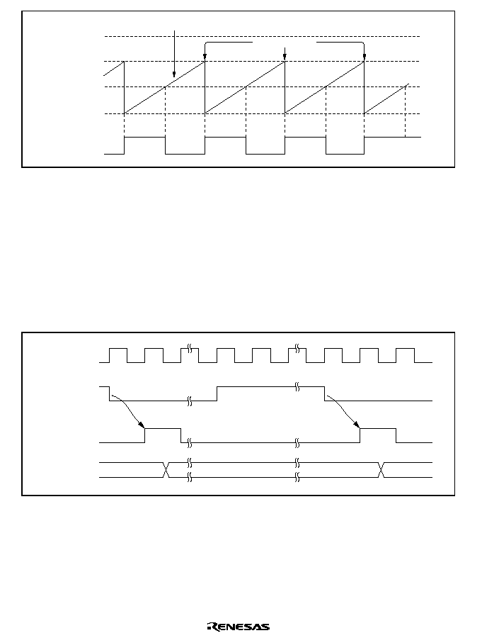
Rev. 2.0, 04/02, page 608 of 906
TCNT
H'FF
Counter clear
TCORA
TCORB
H'00
TMO
Figure 13.2 Example of Pulse Output
13.5
Operation Timing
13.5.1
TCNT Incrementation Timing
Figure 13.3 shows the count timing for internal clock input. Figure 13.4 shows the count timing
for external clock signal. Note that the external clock pulse width must be at least 1.5 states for
incrementation at a single edge, and at least 2.5 states for incrementation at both edges. The
counter will not increment correctly if the pulse width is less than these values.
¯
Internal clock
Clock input
to TCNT
TCNT
N≠1
N
N+1
Figure 13.3 Count Timing for Internal Clock Input

Rev. 2.0, 04/02, page 609 of 906
¯
External clock
input pin
Clock input
to TCNT
TCNT
N≠1
N
N+1
Figure 13.4 Count Timing for External Clock Input
13.5.2
Timing of CMFA and CMFB Setting when Compare-Match Occurs
The CMFA and CMFB flags in TCSR are set to 1 by a compare match signal generated when the
TCOR and TCNT values match. The compare match signal is generated at the last state in which
the match is true, just before the timer counter is updated. Therefore, when TCOR and TCNT
match, the compare match signal is not generated until the next incrementation clock input.
Figure 13.5 shows this timing.
¯
TCNT
N
N+1
TCOR
N
Compare match
signal
CMF
Figure 13.5 Timing of CMF Setting
13.5.3
Timing of Timer Output when Compare-Match Occurs
When compare match A or B occurs, the timer output changes as specified by bits OS3 to OS0 in
TCSR.
Figure 13.6 shows the timing when the output is set to toggle at compare match A.
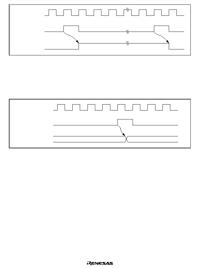
Rev. 2.0, 04/02, page 610 of 906
¯
Compare match A
signal
Timer output pin
Figure 13.6 Timing of Timer Output
13.5.4
Timing of Compare Match Clear
TCNT is cleared when compare match A or B occurs, depending on the setting of the CCLR1 and
CCLR0 bits in TCR. Figure 13.7 shows the timing of this operation.
¯
N
H'00
Compare match
signal
TCNT
Figure 13.7 Timing of Compare Match Clear
13.5.5
Timing of TCNT External Reset
TCNT is cleared at the rising edge of an external reset input, depending on the settings of the
CCLR1 and CCLR0 bits in TCR. The clear pulse width must be at least 1.5 states. Figure 13.8
shows the timing of this operation.
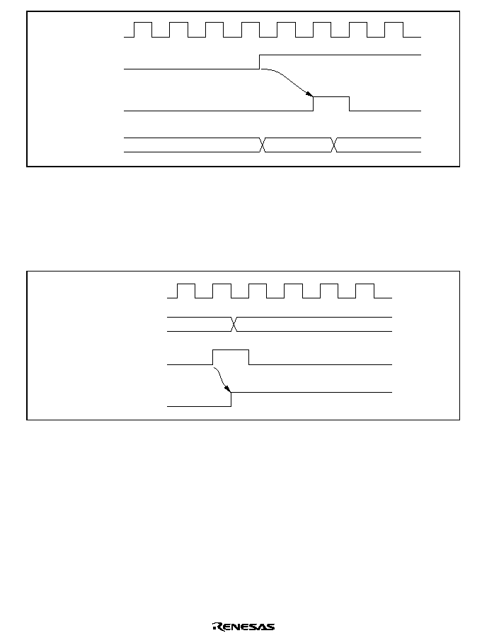
Rev. 2.0, 04/02, page 611 of 906
¯
Clear signal
External reset
input pin
TCNT
N
H'00
N≠1
Figure 13.8 Timing of Clearance by External Reset
13.5.6
Timing of Overflow Flag (OVF) Setting
The OVF in TCSR is set to 1 when TCNT overflows (changes from H'FF to H'00). Figure 13.9
shows the timing of this operation.
¯
OVF
Overflow signal
TCNT
H'FF
H'00
Figure 13.9 Timing of OVF Setting
13.6
Operation with Cascaded Connection
If bits CKS2 to CKS0 in either TCR_0 or TCR_1 are set to B'100, the 8-bit timers of the two
channels are cascaded. With this configuration, a single 16-bit timer could be used (16-bit counter
mode) or compare matches of the 8-bit channel 0 could be counted by the timer of channel 1
(compare match count mode). In this case, the timer operates as below.
13.6.1
16-Bit Counter Mode
When bits CKS2 to CKS0 in TCR_0 are set to B'100, the timer functions as a single 16-bit timer
with channel 0 occupying the upper 8 bits and channel 1 occupying the lower 8 bits.

Rev. 2.0, 04/02, page 612 of 906
[1] Setting of compare match flags
∑
The CMF flag in TCSR_0 is set to 1 when a 16-bit compare match event occurs.
∑
The CMF flag in TCSR_1 is set to 1 when a lower 8-bit compare match event occurs.
[2] Counter clear specification
∑
If the CCLR1 and CCLR0 bits in TCR_0 have been set for counter clear at compare match, the
16-bit counters (TCNT_0 and TCNT_1 together) are cleared when a 16-bit compare match
event occurs. The 16-bit counters (TCNT0 and TCNT1 together) are cleared even if counter
clear by the TMRI0 pin has also been set.
∑
The settings of the CCLR1 and CCLR0 bits in TCR_1 are ignored. The lower 8 bits cannot be
cleared independently.
[3] Pin output
∑
Control of output from the TMO0 pin by bits OS3 to OS0 in TCSR_0 is in accordance with the
16-bit compare match conditions.
∑
Control of output from the TMO1 pin by bits OS3 to OS0 in TCSR_1 is in accordance with the
lower 8-bit compare match conditions.
13.6.2
Compare Match Count Mode
When bits CKS2 to CKS0 in TCR_1 are B'100, TCNT_1 counts compare match A's for channel
0.
Channels 0 and 1 are controlled independently. Conditions such as setting of the CMF flag,
generation of interrupts, output from the TMO pin, and counter clear are in accordance with the
settings for each channel.
13.7
Interrupts
13.7.1
Interrupt Sources and DTC Activation
There are three 8-bit timer interrupt sources: CMIA, CMIB, and OVI. Their relative priorities are
shown in table 13.3. Each interrupt source is set as enabled or disabled by the corresponding
interrupt enable bit in TCR or TCSR, and independent interrupt requests are sent for each to the
interrupt controller. It is also possible to activate the DTC by means of CMIA and CMIB
interrupts.

Rev. 2.0, 04/02, page 613 of 906
Table 13.3
8-Bit Timer Interrupt Sources
Name
Interrupt Source
Interrupt Flag
DTC Activation
Priority
CMIA0
TCORA_0 compare match
CMFA
Possible
High
CMIB0
TCORB_0 compare match
CMFB
Possible
OVI0
TCNT_0 overflow
OVF
Not possible
Low
CMIA1
TCORA_1 compare match
CMFA
Possible
High
CMIB1
TCORB_1 compare match
CMFB
Possible
OVI1
TCNT_1 overflow
OVF
Not possible
Low
13.7.2
A/D Converter Activation
The A/D converter can be activated only by TMR_0 compare match A.
If the ADTE bit in TCSR0 is set to 1 when the CMFA flag is set to 1 by the occurrence of TMR_0
compare match A, a request to start A/D conversion is sent to the A/D converter. If the 8-bit timer
conversion start trigger has been selected on the A/D converter side at this time, A/D conversion is
started.

Rev. 2.0, 04/02, page 614 of 906
13.8
Usage Notes
13.8.1
Contention between TCNT Write and Clear
If a timer counter clock pulse is generated during the T
2
state of a TCNT write cycle, the clear
takes priority, so that the counter is cleared and the write is not performed.
Figure 13.10 shows this operation.
¯
Address
TCNT address
Internal write signal
Counter clear signal
TCNT
N
H'00
T
1
T
2
TCNT write cycle by CPU
Figure 13.10 Contention between TCNT Write and Clear
13.8.2
Contention between TCNT Write and Increment
If a timer counter clock pulse is generated during the T
2
state of a TCNT write cycle, the write
takes priority and the counter is not incremented.
Figure 13.11 shows this operation.

Rev. 2.0, 04/02, page 615 of 906
¯
Address
TCNT address
Internal write signal
TCNT input clock
TCNT
N
M
T
1
T
2
TCNT write cycle by CPU
Counter write data
Figure 13.11 Contention between TCNT Write and Increment
13.8.3
Contention between TCOR Write and Compare Match
During the T
2
state of a TCOR write cycle, the TCOR write has priority and the compare match
signal is inhibited even if a compare match event occurs as shown in figure 13.12.
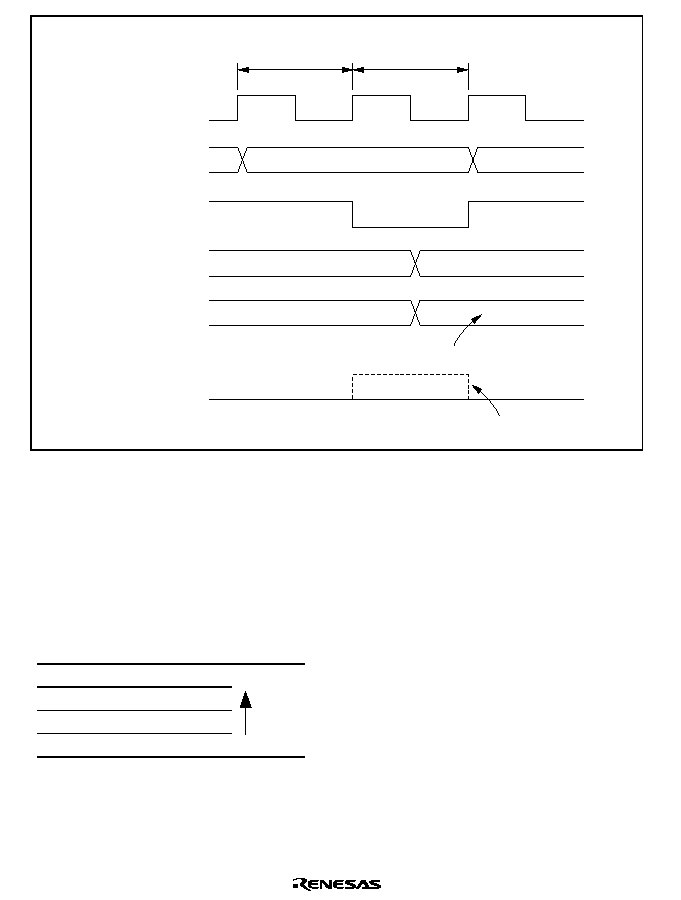
Rev. 2.0, 04/02, page 616 of 906
¯
Address
TCOR address
Internal write signal
TCNT
TCOR
N
M
T
1
T
2
TCOR write cycle by CPU
TCOR write data
N
N+1
Compare match signal
Inhibited
Figure 13.12 Contention between TCOR Write and Compare Match
13.8.4
Contention between Compare Matches A and B
If compare match events A and B occur at the same time, the 8-bit timer operates in accordance
with the priorities for the output statuses set for compare match A and compare match B, as shown
in table 13.4.
Table 13.4
Timer Output Priorities
Output Setting
Priority
Toggle output
High
1 output
0 output
No change
Low

Rev. 2.0, 04/02, page 617 of 906
13.8.5
Switching of Internal Clocks and TCNT Operation
TCNT may increment erroneously when the internal clock is switched over. Table 13.5 shows the
relationship between the timing at which the internal clock is switched (by writing to the CKS1
and CKS0 bits) and the TCNT operation.
When the TCNT clock is generated from an internal clock, the falling edge of the internal clock
pulse is detected. If clock switching causes a change from high to low level, as shown in case 3 in
table 13.5, a TCNT clock pulse is generated on the assumption that the switchover is a falling
edge. This increments TCNT.
The erroneous incrementation can also happen when switching between internal and external
clocks.
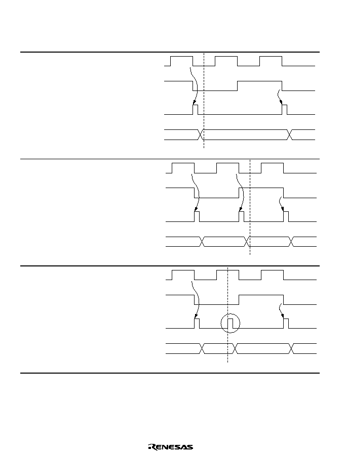
Rev. 2.0, 04/02, page 618 of 906
Table 13.5
Switching of Internal Clock and TCNT Operation
No.
Timing of Switchover
by Means of CKS1
and CKS0 Bits
TCNT Clock Operation
1
Switching from
low to low
*
1
Clock before
switchover
Clock after
switchover
TCNT clock
TCNT
CKS bit write
N
N + 1
2
Switching from
low to high
*
2
Clock before
switchover
Clock after
switchover
TCNT clock
TCNT
CKS bit write
N
N + 1
N + 2
3
Switching from
high to low
*
3
Clock before
swichover
Clock after
swichover
TCNT clock
TCNT
CKS bit write
N
N + 1
N + 2
*
4
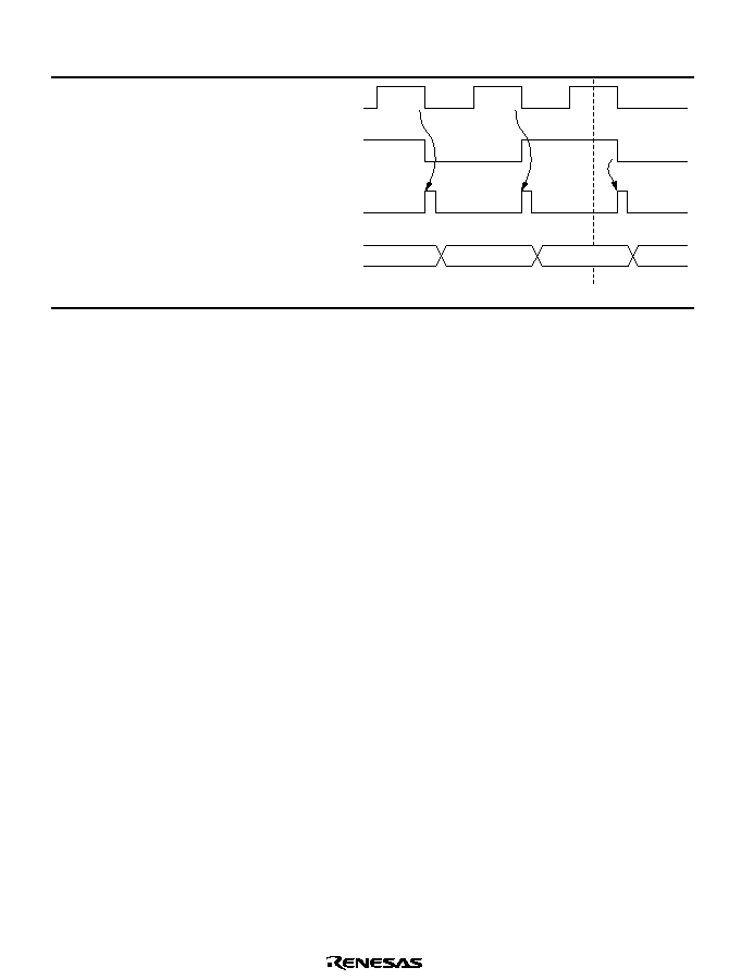
Rev. 2.0, 04/02, page 619 of 906
No.
Timing of Switchover
by Means of CKS1
and CKS0 Bits
TCNT Clock Operation
4
Switching from high
to high
Clock before
switchover
Clock after
switchover
TCNT clock
TCNT
CKS bit write
N
N + 1
N + 2
Notes: 1. Includes switching from low to stop, and from stop to low.
2. Includes switching from stop to high.
3. Includes switching from high to stop.
4. Generated on the assumption that the switchover is a falling edge; TCNT is
incremented.
13.8.6
Mode Setting with Cascaded Connection
If 16-bit counter mode and compare match count mode are specified at the same time, input clocks
for TCNT_0 and TCNT_1 are not generated, and the counter stops. Do not specify 16-bit counter
and compare match count modes simultaneously.
13.8.7
Interrupts in Module Stop Mode
If module stop mode is entered when an interrupt has been requested, it will not be possible to
clear the CPU interrupt source or the DTC and DMAC activation source. Interrupts should
therefore be disabled before entering module stop mode.

Rev. 2.0, 04/02, page 620 of 906

Rev. 2.0, 04/02, page 621 of 906
Section 14 Watchdog Timer
The watchdog timer (WDT) is an 8-bit timer that outputs an overflow signal (
:'729)) if a
system crash prevents the CPU from writing to the timer counter, thus allowing it to overflow.
At the same time, the WDT can also generate an internal reset signal.
When this watchdog function is not needed, the WDT can be used as an interval timer. In interval
timer operation, an interval timer interrupt is generated each time the counter overflows.
The block diagram of the WDT is shown in figure 14.1.
14.1
Features
∑
Selectable from eight counter input clocks
∑
Switchable between watchdog timer mode and interval timer mode
In watchdog timer mode
∑
If the counter overflows, the WDT outputs
:'729). It is possible to select whether or not
the entire chip is reset at the same time.
In interval timer mode
∑
If the counter overflows, the WDT generates an interval timer interrupt (WOVI).
WDT0101A_010020020400
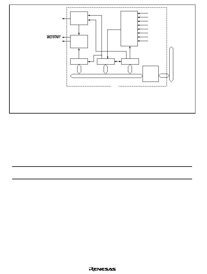
Rev. 2.0, 04/02, page 622 of 906
Overflow
Interrupt
control
WOVI
(interrupt request
signal)
Internal reset signal
*
Reset
control
RSTCSR
TCNT
TSCR
¯/2
¯/64
¯/128
¯/512
¯/2048
¯/8192
¯/32768
¯/131072
Clock
Clock
select
Internal clock
sources
Bus
interface
Module bus
TCSR
TCNT
RSTCSR
Note:
*
An internal reset signal can be generated by the register setting.
: Timer control/status register
: Timer counter
: Reset control/status register
WDT
Legend
Internal bus
Figure 14.1 Block Diagram of WDT
14.2
Input/Output Pin
Table 14.1 shows the WDT pin configuration.
Table 14.1
Pin configuration
Name
Symbol
I/O
Function
Watchdog timer overflow
:'729)
Output
Outputs counter overflow signal in watchdog
timer mode
14.3
Register Descriptions
The WDT has the following three registers. To prevent accidental overwriting, TCSR, TCNT, and
RSTCSR have to be written to in a method different from normal registers. For details, refer to
section 14.6.1, Notes on Register Access.
∑
Timer counter (TCNT)
∑
Timer control/status register (TCSR)
∑
Reset control/status register (RSTCSR)

Rev. 2.0, 04/02, page 623 of 906
14.3.1
Timer Counter (TCNT)
TCNT is an 8-bit readable/writable up-counter. TCNT is initialized to H'00 when the TME bit in
TCSR is cleared to 0.
14.3.2
Timer Control/Status Register (TCSR)
TCSR selects the clock source to be input to TCNT, and the timer mode.
Bit
Bit Name
Initial Value
R/W
Description
7
OVF
0
R/(W)
*
Overflow Flag
Indicates that TCNT has overflowed in interval
timer mode. Only a write of 0 is permitted, to clear
the flag.
[Setting condition]
When TCNT overflows in interval timer mode
(changes from H'FF to H'00)
When internal reset request generation is selected
in watchdog timer mode, OVF is cleared
automatically by the internal reset.
[Clearing conditions]
Cleared by reading TCSR when OVF = 1, then
writing 0 to OVF
6
WT/
,7
0
R/W
Timer Mode Select
Selects whether the WDT is used as a watchdog
timer or interval timer.
0: Interval timer mode
When TCNT overflows, an interval timer interrupt
(WOVI) is requested.
1: Watchdog timer mode
When TCNT overflows, the
:'729)
signal is
output.
5
TME
0
R/W
Timer Enable
When this bit is set to 1, TCNT starts counting.
When this bit is cleared, TCNT stops counting and
is initialized to H'00.

Rev. 2.0, 04/02, page 624 of 906
Bit
Bit Name
Initial Value
R/W
Description
4
3
--
--
1
1
--
--
Reserved
These bits are always read as 1 and cannot be
modified.
2
1
0
CKS2
CKS1
CKS0
0
0
0
R/W
R/W
R/W
Clock Select 2 to 0
Selects the clock source to be input to TCNT. The
overflow frequency for ¯ = 20 MHz is enclosed in
parentheses.
000: Clock ¯/2 (frequency: 25.6
µ
s)
001: Clock ¯/64 (frequency: 819.2
µ
s)
010: Clock ¯/128 (frequency: 1.6 ms)
011: Clock ¯/512 (frequency: 6.6 ms)
100: Clock ¯/2048 (frequency: 26.2 ms)
101: Clock ¯/8192 (frequency: 104.9 ms)
110: Clock ¯/32768 (frequency: 419.4 ms)
111: Clock ¯/131072 (frequency: 1.68 s)
Note: Only a write of 0 is permitted, to clear the flag.

Rev. 2.0, 04/02, page 625 of 906
14.3.3
Reset Control/Status Register (RSTCSR)
RSTCSR controls the generation of the internal reset signal when TCNT overflows, and selects
the type of internal reset signal. RSTCSR is initialized to H'1F by a reset signal from the
5(6 pin,
but not by the WDT internal reset signal caused by overflows.
Bit
Bit Name
Initial Value
R/W
Description
7
WOVF
0
R/(W)
*
Watchdog Timer Overflow Flag
This bit is set when TCNT overflows in watchdog
timer mode. This bit cannot be set in interval
timer mode, and only 0 can be written.
[Setting condition]
Set when TCNT overflows (changed from H'FF to
H'00) in watchdog timer mode
[Clearing condition]
Cleared by reading RSTCSR when WOVF = 1,
and then writing 0 to WOVF
6
RSTE
0
R/W
Reset Enable
Specifies whether or not a reset signal is
generated in the chip if TCNT overflows during
watchdog timer operation.
0: Reset signal is not generated even if TCNT
overflows
(Though this LSI is not reset, TCNT and TCSR in
WDT are reset)
1: Reset signal is generated if TCNT overflows
5
--
0
R/W
Reserved
Can be read and written, but does not affect
operation.
4
to
0
--
1
--
Reserved
These bits are always read as 1 and cannot be
modified.
Note: Only a write of 0 is permitted, to clear the flag.

Rev. 2.0, 04/02, page 626 of 906
14.4
Operation
14.4.1
Watchdog Timer Mode
To use the WDT as a watchdog timer mode, set the WT/
,7 and TME bits in TCSR to 1.
If TCNT overflows without being rewritten because of a system crash or other error, the
:'729) signal is output.
This ensures that TCNT does not overflow while the system is operating normally. Software must
prevent TCNT overflows by rewriting the TCNT value (normally be writing H'00) before
overflow occurs. This
:'729) signal can be used to reset the chip internally in watchdog timer
mode.
If TCNT overflows when 1 is set in the RSTE bit in RSTCSR, a signal that resets this LSI
internally is generated at the same time as the
:'729) signal. If a reset caused by a signal input
to the
5(6 pin occurs at the same time as a reset caused by a WDT overflow, the 5(6 pin reset
has priority and the WOVF bit in RSTCSR is cleared to 0.
The
:'729) signal is output for 132 states when RSTE = 1, and for 130 states when RSTE = 0.
The internal reset signal is output for 518 states.
When TCNT overflows in watchdog timer mode, the WOVF bit in RSTCSR is set to 1. If TCNT
overflows when 1 is set in the RSTE bit in RSTCSR, an internal reset signal is generated to the
entire chip.
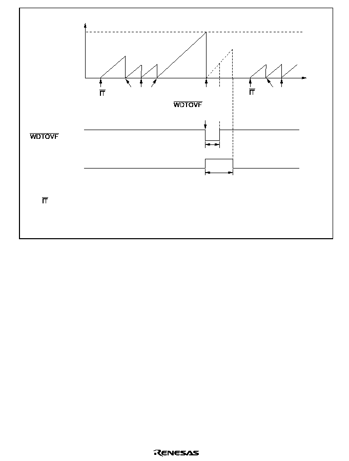
Rev. 2.0, 04/02, page 627 of 906
TCNT count
H'00
Time
H'FF
WT/ =1
TME=1
H'00 written
to TCNT
WT/ =1
TME=1
H'00 written
to TCNT
132 states
*
2
518 states
signal
Internal reset signal
*
1
WT/
TME
Notes: 1. If TCNT overflows when the RSTE bit is set to 1, an internal reset signal is generated.
2. 130 states when the RSTE bit is cleared to 0.
Overflow
and
internal reset are
generated
WOVF=1
: Timer mode select bit
: Timer enable bit
Legend
Figure 14.2 Operation in Watchdog Timer Mode
14.4.2
Interval Timer Mode
To use the WDT as an interval timer, set the WT/
,7 bit to 0 and TME bit in TCSR to 1.
When the WDT is used as an interval timer, an interval timer interrupt (WOVI) is generated each
time the TCNT overflows. Therefore, an interrupt can be generated at intervals.
When the TCNT overflows in interval timer mode, an interval timer interrupt (WOVI) is requested
at the same time the OVF bit in the TCSR is set to 1.
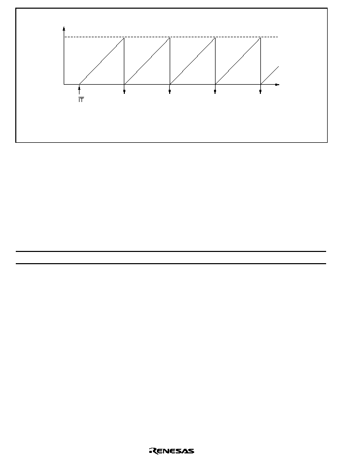
Rev. 2.0, 04/02, page 628 of 906
TCNT count
H'00
Time
H'FF
WT/ =0
TME=1
WOVI
Overflow
Overflow
Overflow
Overflow
Legend
WOVI: Interval timer interrupt request generation
WOVI
WOVI
WOVI
Figure 14.3 Operation in Interval Timer Mode
14.5
Interrupt Source
During interval timer mode operation, an overflow generates an interval timer interrupt (WOVI).
The interval timer interrupt is requested whenever the OVF flag is set to 1 in TCSR. OVF must be
cleared to 0 in the interrupt handling routine.
Table 14.2
WDT Interrupt Source
Name
Interrupt Source
Interrupt Flag
DTC Activation
WOVI
TCNT overflow
OVF
Impossible
14.6
Usage Notes
14.6.1
Notes on Register Access
The watchdog timer's TCNT, TCSR, and RSTCSR registers differ from other registers in being
more difficult to write to. The procedures for writing to and reading these registers are given
below.
Writing to TCNT, TCSR, and RSTCSR
TCNT and TCSR must be written to by a word transfer instruction. They cannot be written to by a
byte transfer instruction.
TCNT and TCSR both have the same write address. Therefore, satisfy the relative condition
shown in figure 14.4 to write to TCNT or TCSR. The transfer instruction writes the lower byte
data to TCNT or TCSR according to the satisfied condition.

Rev. 2.0, 04/02, page 629 of 906
To write to RSTCSR, execute a word transfer instruction for address H'FFBE. A byte transfer
instruction cannot perform writing to RSTCSR.
The method of writing 0 to the WOVF bit differs from that of writing to the RSTE bit. To write 0
to the WOVF bit, satisfy the lower condition shown in figure 14.4.
If satisfied, the transfer instruction clears the WOVF bit to 0, but has no effect on the RSTE bit.
To write to the RSTE bit, satisfy the above condition shown in figure 14.4. If satisfied, the transfer
instruction writes the value in bit 6 of the lower byte into the RSTE bit, but has no effect on the
WOVF bit.
TCNT write or
Writing to RSTE bit in RSTCSR
TCSR write
Address:
H'FFBC (TCNT)
H'FFBE (RSTCSR)
15
8
7
0
H'5A
Write data
Address:
H'FFBC (TCSR)
15
8
7
0
H'A5
Write data
Writing 0 to WOVF bit in RSTCSR
Address:
H'FFBE (RSTCSR)
15
8
7
0
H'A5
H'00
Figure 14.4 Writing to TCNT, TCSR, and RSTCSR
Reading TCNT, TCSR, and RSTCSR
These registers are read in the same way as other registers. The read addresses are H'FFBC for
TCSR, H'FFBD for TCNT, and H'FFBF for RSTCSR.
14.6.2
Contention between Timer Counter (TCNT) Write and Increment
If a timer counter clock pulse is generated during the next cycle after the T2 state of a TCNT write
cycle, the write takes priority and the timer counter is not incremented. Figure 14.5 shows this
operation.
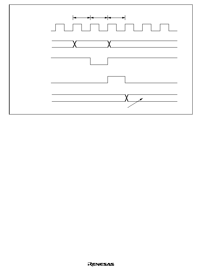
Rev. 2.0, 04/02, page 630 of 906
Address
¯
Internal write signal
TCNT input clock
TCNT
N
M
T1
T2
Next cycle
TCNT write cycle
Counter write data
Figure 14.5 Contention between TCNT Write and Increment
14.6.3
Changing Value of CKS2 to CKS0
If bits CKS2 to CKS0 in TCSR are written to while the WDT is operating, errors could occur in
the incrementation. Software must stop the watchdog timer (by clearing the TME bit to 0) before
changing the value of bits CKS2 to CKS0.
14.6.4
Switching between Watchdog Timer Mode and Interval Timer Mode
If the mode is switched from watchdog timer to interval timer, while the WDT is operating, errors
could occur in the incrementation. Software must stop the watchdog timer (by clearing the TME
bit to 0) before switching the mode.
14.6.5
Internal Reset in Watchdog Timer Mode
This LSI is not reset internally if TCNT overflows while the RSTE bit is cleared to 0 during
watchdog timer mode operation, but TCNT and TCSR of the WDT are reset.
TCNT, TCSR, and RSTCR cannot be written to while the
:'729) signal is low. Also note that
a read of the WOVF flag is not recognized during this period. To clear the WOVF flag, therefore,
read TCSR after the
:'729) signal goes high, then write 0 to the WOVF flag.
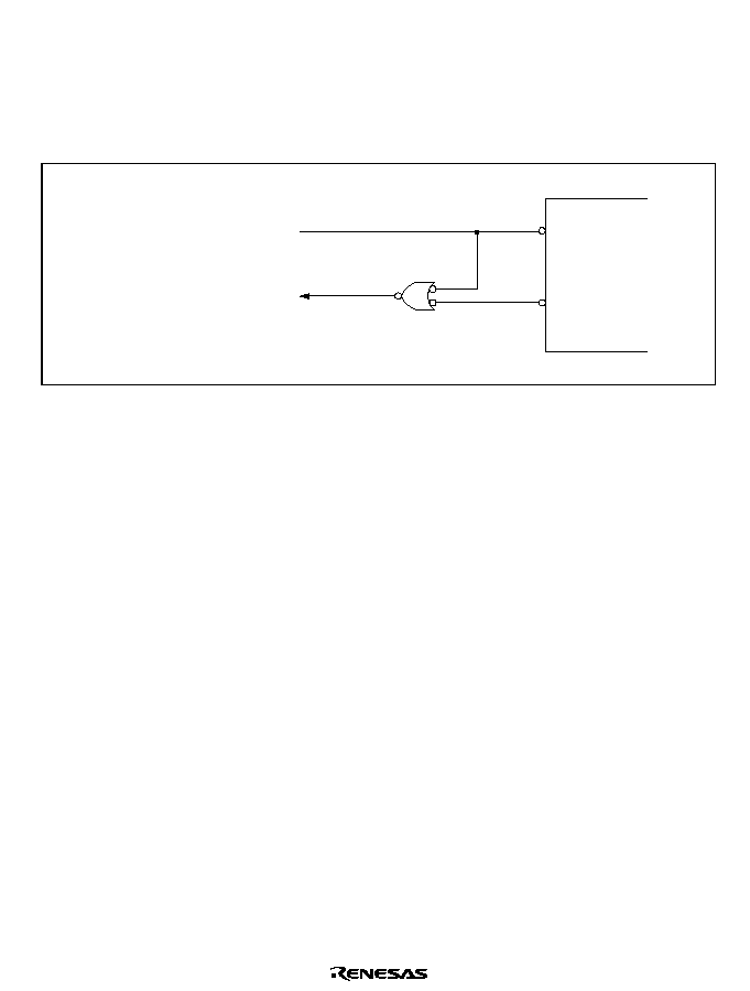
Rev. 2.0, 04/02, page 631 of 906
14.6.6
System Reset by
:'729)
:'729) Signal
If the
:'729) output signal is input to the 5(6 pin, the chip will not be initialized correctly.
Make sure that the
:'729) signal is not input logically to the 5(6 pin.
To reset the entire system by means of the
:'729) signal, use the circuit shown in figure 14.6.
Reset input
Reset signal to entire system
This LSI
RES
WDTOVF
Figure 14.6 Circuit for System Reset by
:'729)
:'729) Signal (Example)

Rev. 2.0, 04/02, page 632 of 906

Rev. 2.0, 04/02, page 633 of 906
Section 15 Serial Communication Interface (SCI, IrDA)
This LSI has three independent serial communication interface (SCI) channels. The SCI can
handle both asynchronous and clocked synchronous serial communication. Serial data
communication can be carried out with standard asynchronous communication chips such as a
Universal Asynchronous Receiver/Transmitter (UART) or Asynchronous Communication
Interface Adapter (ACIA). A function is also provided for serial communication between
processors (multiprocessor communication function) in asynchronous mode. The SCI also
supports an IC card (Smart Card) interface conforming to ISO/IEC 7816-3 (Identification Card) as
an asynchronous serial communication interface extension function. One of the three SCI channels
(SCI_0) can generate an IrDA communication waveform conforming to IrDA specification
version 1.0.
Figure 15.1 shows a block diagram of the SCI.
15.1
Features
∑
Choice of asynchronous or clocked synchronous serial communication mode
∑
Full-duplex communication capability
The transmitter and receiver are mutually independent, enabling transmission and reception to
be executed simultaneously. Double-buffering is used in both the transmitter and the receiver,
enabling continuous transmission and continuous reception of serial data.
∑
On-chip baud rate generator allows any bit rate to be selected
External clock can be selected as a transfer clock source (except for in Smart Card interface
mode).
∑
Choice of LSB-first or MSB-first transfer (except in the case of asynchronous mode 7-bit data)
∑
Four interrupt sources
Four interrupt sources -- transmit-end, transmit-data-empty, receive-data-full, and receive
error -- that can issue requests. The transmit-data-empty interrupt and receive data full
interrupts can activate the data transfer controller (DTC) or DMA controller (DMAC).
∑
Module stop mode can be set
Asynchronous mode
∑
Data length: 7 or 8 bits
∑
Stop bit length: 1 or 2 bits
∑
Parity: Even, odd, or none
∑
Receive error detection: Parity, overrun, and framing errors
∑
Break detection: Break can be detected by reading the RxD pin level directly in case of a
framing error
SCI0020A_000020020400

Rev. 2.0, 04/02, page 634 of 906
∑
Average transfer rate generator (only for H8S/2678R Series): The following transfer rate can
be selected (SCI_2 only)
115.152 or 460.606 kbps at 10.667 MHz operation
115.196, 460.784 or 720 kbps at 16 MHz operation
720 kbps at 32 MHz operation
Clocked Synchronous mode
∑
Data length: 8 bits
∑
Receive error detection: Overrun errors detected
Smart Card Interface
∑
Automatic transmission of error signal (parity error) in receive mode
∑
Error signal detection and automatic data retransmission in transmit mode
∑
Direct convention and inverse convention both supported
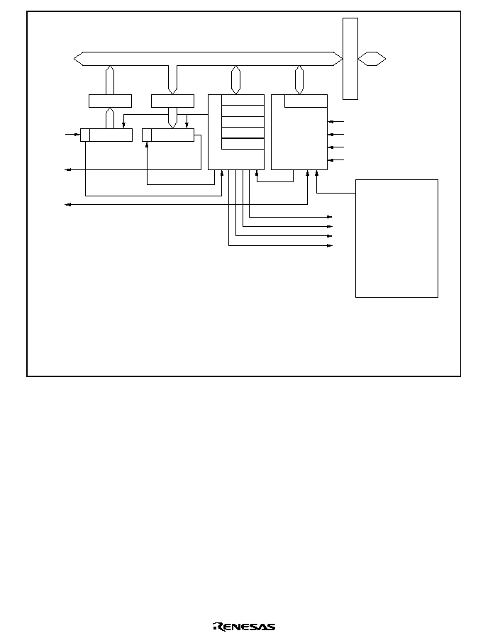
Rev. 2.0, 04/02, page 635 of 906
RxD
TxD
SCK
Clock
External clock
/4
/16
/64
TEI
TXI
RXI
ERI
SCMR
SSR
SCR
SMR
SEMR
*
Transmission/
reception control
Baud rate
generator
BRR
Module data bus
RDR
TSR
RSR
Parity generation
Parity check
TDR
Bus interface
Internal
data bus
Average transfer
rate generator
*
(SCI_2)
10.667 MHz operation
∑ 115.152 kbps
∑ 460.606 kbps
16 MHz operation
∑ 115.196 kbps
∑ 460.784 kbps
∑ 720 kbps
32 MHz operation
∑ 720 kbps
Legend
RSR
: Receive shift register
RDR
: Receive data register
TSR
: Transmit shift register
TDR
: Transmit data register
SMR
: Serial mode register
SCR
: Serial control register
SSR
: Serial status register
SCMR
: Smart card mode register
BRR
: Bit rate register
SEMR
: Serial extension mode register (only in SCI_2)
Note:
*
Only in H8S/2678R series.
Figure 15.1 Block Diagram of SCI
15.2
Input/Output Pins
Table 15.1 shows the pin configuration of the serial communication interface.

Rev. 2.0, 04/02, page 636 of 906
Table 15.1
Pin Configuration
Channel
Pin Name
*
I/O
Function
SCK0
I/O
Channel 0 clock input/output
RxD0/IrRxD
Input
Channel 0 receive data input (normal/IrDA)
0
TxD0/IrTxD
Output
Channel 0 transmit data output (normal/IrDA)
SCK1
I/O
Channel 1 clock input/output
RxD1
Input
Channel 1 receive data input
1
TxD1
Output
Channel 1 transmit data output
SCK2
I/O
Channel 2 clock input/output
RxD2
Input
Channel 2 receive data input
2
TxD2
Output
Channel 2 transmit data output
Note: Pin names SCK, RxD, and TxD are used in the text for all channels, omitting the channel
designation.
15.3
Register Descriptions
The SCI has the following registers. The serial mode register (SMR), serial status register (SSR),
and serial control register (SCR) are described separately for normal serial communication
interface mode and Smart Card interface mode because their bit functions partially differ.
∑
Receive shift register_0 (RSR_0)
∑
Transmit shift register_0 (TSR_0)
∑
Receive data register_0 (RDR_0)
∑
Transmit data register_0 (TDR_0)
∑
Serial mode register_0 (SMR_0)
∑
Serial control register_0 (SCR_0)
∑
Serial status register_0 (SSR_0)
∑
Smart card mode register_0 (SCMR_0)
∑
Bit rate register_0 (BRR_0)
∑
IrDA control register_0 (IrCR_0)
∑
Receive shift register_1 (RSR_1)
∑
Transmit shift register_1 (TSR_1)
∑
Receive data register_1 (RDR_1)
∑
Transmit data register_1 (TDR_1)
∑
Serial mode register_1 (SMR_1)
∑
Serial control register_1 (SCR_1)
∑
Serial status register_1 (SSR_1)

Rev. 2.0, 04/02, page 637 of 906
∑
Smart card mode register_1 (SCMR_1)
∑
Bit rate register_1 (BRR_1)
∑
Receive shift register_2 (RSR_2)
∑
Transmit shift register_2 (TSR_2)
∑
Receive data register_2 (RDR_2)
∑
Transmit data register_2 (TDR_2)
∑
Serial mode register_2 (SMR_2)
∑
Serial control register_2 (SCR_2)
∑
Serial status register_2 (SSR_2)
∑
Smart card mode register_2 (SCMR_2)
∑
Bit rate register_2 (BRR_2)
∑
Serial extension mode register (SEMR)*
Note: Only in H8S/2678R Series.
15.3.1
Receive Shift Register (RSR)
RSR is a shift register used to receive serial data that is input to the RxD pin and convert it into
parallel data. When one byte of data has been received, it is transferred to RDR automatically.
RSR cannot be directly accessed by the CPU.
15.3.2
Receive Data Register (RDR)
RDR is an 8-bit register that stores receive data. When the SCI has received one byte of serial
data, it transfers the received serial data from RSR to RDR where it is stored. After this, RSR is
receive-enabled. Since RSR and RDR function as a double buffer in this way, enables continuous
receive operations to be performed. After confirming that the RDRF bit in SSR is set to 1, read
RDR for only once. RDR cannot be written to by the CPU.
15.3.3
Transmit Data Register (TDR)
TDR is an 8-bit register that stores transmit data. When the SCI detects that TSR is empty, it
transfers the transmit data written in TDR to TSR and starts transmission. The double-buffered
structures of TDR and TSR enable continuous serial transmission. If the next transmit data has
already been written to TDR during serial transmission, the SCI transfers the written data to TSR
to continue transmission. Although TDR can be read or written to by the CPU at all times, to
achieve reliable serial transmission, write transmit data to TDR for only once after confirming that
the TDRE bit in SSR is set to 1.

Rev. 2.0, 04/02, page 638 of 906
15.3.4
Transmit Shift Register (TSR)
TSR is a shift register that transmits serial data. To perform serial data transmission, the SCI first
transfers transmit data from TDR to TSR, then sends the data to the TxD pin starting. TSR cannot
be directly accessed by the CPU.
15.3.5
Serial Mode Register (SMR)
SMR is used to set the SCI's serial transfer format and select the on-chip baud rate generator clock
source.
Some bit functions of SMR differ in normal serial communication interface mode and Smart Card
interface mode.

Rev. 2.0, 04/02, page 639 of 906
Normal Serial Communication Interface Mode (When SMIF in SCMR is 0)
Bit
Bit Name
Initial Value
R/W
Description
7
C/
0
R/W
Communication Mode
0: Asynchronous mode
1: Clocked synchronous mode
6
CHR
0
R/W
Character Length (enabled only in asynchronous
mode)
0: Selects 8 bits as the data length.
1: Selects 7 bits as the data length. LSB-first is
fixed and the MSB (bit 7) of TDR is not transmitted
in transmission.
In clocked synchronous mode, a fixed data length
of 8 bits is used.
5
PE
0
R/W
Parity Enable (enabled only in asynchronous
mode)
When this bit is set to 1, the parity bit is added to
transmit data before transmission, and the parity
bit is checked in reception. For a multiprocessor
format, parity bit addition and checking are not
performed regardless of the PE bit setting.
4
O/
0
R/W
Parity Mode (enabled only when the PE bit is 1 in
asynchronous mode)
0: Selects even parity.
1: Selects odd parity.
3
STOP
0
R/W
Stop Bit Length (enabled only in asynchronous
mode)
Selects the stop bit length in transmission.
0: 1 stop bit
1: 2 stop bits
In reception, only the first stop bit is checked
regardless of the STOP bit setting. If the second
stop bit is 0, it is treated as the start bit of the next
transmit character.
2
MP
0
R/W
Multiprocessor Mode (enabled only in
asynchronous mode)
When this bit is set to 1, the multiprocessor
communication function is enabled. The PE bit
and O/
bit settings are invalid in multiprocessor
mode.

Rev. 2.0, 04/02, page 640 of 906
Bit
Bit Name
Initial Value
R/W
Description
1
0
CKS1
CKS0
0
0
R/W
R/W
Clock Select 1 and 0:
These bits select the clock source for the on-chip
baud rate generator.
00: ¯ clock (n = 0)
01: ¯/4 clock (n = 1)
10: ¯/16 clock (n = 2)
11: ¯/64 clock (n = 3)
For the relation between the bit rate register
setting and the baud rate, see section 15.3.9, Bit
Rate Register (BRR). n is the decimal display of
the value of n in BRR (see section 15.3.9, Bit Rate
Register (BRR)).
Smart Card Interface Mode (When SMIF in SCMR is 1)
Bit
Bit Name
Initial Value
R/W
Description
7
GM
0
R/W
GSM Mode
When this bit is set to 1, the SCI operates in GSM
mode. In GSM mode, the timing of the TEND
setting is advanced by 11.0 etu (Elementary Time
Unit: the time for transfer of one bit), and clock
output control mode addition is performed. For
details, refer to section 15.7.8, Clock Output
Control.
6
BLK
0
R/W
When this bit is set to 1, the SCI operates in block
transfer mode. For details on block transfer mode,
refer to section 15.7.3, Block Transfer Mode.
5
PE
0
R/W
Parity Enable (enabled only in asynchronous
mode)
When this bit is set to 1, the parity bit is added to
transmit data before transmission, and the parity
bit is checked in reception. In Smart Card
interface mode, this bit must be set to 1.
4
O/
0
R/W
Parity Mode (enabled only when the PE bit is 1 in
asynchronous mode)
0: Selects even parity.
1: Selects odd parity.
For details on setting this bit in Smart Card
interface mode, refer to section 15.7.2, Data
Format (Except for Block Transfer Mode).

Rev. 2.0, 04/02, page 641 of 906
Bit
Bit Name
Initial Value
R/W
Description
3
2
BCP1
BCP0
0
0
R/W
R/W
Basic Clock Pulse 1 and 0
These bits select the number of basic clock
periods in a 1-bit transfer interval on the Smart
Card interface.
00: 32 clock (S = 32)
01: 64 clock (S = 64)
10: 372 clock (S = 372)
11: 256 clock (S = 256)
For details, refer to section 15.7.4, Receive Data
Sampling Timing and Reception Margin. S stands
for the value of S in BRR (see section 15.3.9, Bit
Rate Register (BRR)).
1
0
CKS1
CKS0
0
0
R/W
R/W
Clock Select 1 and 0:
These bits select the clock source for the on-chip
baud rate generator.
00: ¯ clock (n = 0)
01: ¯/4 clock (n = 1)
10: ¯/16 clock (n = 2)
11: ¯/64 clock (n = 3)
For the relation between the bit rate register
setting and the baud rate, see section 15.3.9, Bit
Rate Register (BRR). n is the decimal display of
the value of n in BRR (see section 15.3.9, Bit Rate
Register (BRR)).
15.3.6
Serial Control Register (SCR)
SCR performs enabling or disabling of SCI transfer operations and interrupt requests, and
selection of the transfer/receive clock source. For details on interrupt requests, refer to section
15.9, Interrupts Sources. Some bit functions of SCR differ in normal serial communication
interface mode and Smart Card interface mode.

Rev. 2.0, 04/02, page 642 of 906
Normal Serial Communication Interface Mode (When SMIF in SCMR is 0)
Bit
Bit Name
Initial Value
R/W
Description
7
TIE
0
R/W
Transmit Interrupt Enable
When this bit is set to 1, TXI interrupt request is
enabled.
6
RIE
0
R/W
Receive Interrupt Enable
When this bit is set to 1, RXI and ERI interrupt
requests are enabled.
5
TE
0
R/W
Transmit Enable
When this bit s set to 1, transmission is enabled.
4
RE
0
R/W
Receive Enable:
When this bit is set to 1, reception is enabled.
3
MPIE
0
R/W
Multiprocessor Interrupt Enable (enabled only
when the MP bit in SMR is 1 in asynchronous
mode)
When this bit is set to 1, receive data in which the
multiprocessor bit is 0 is skipped, and setting of
the RDRF, FER, and ORER status flags in SSR is
prohibited. On receiving data in which the
multiprocessor bit is 1, this bit is automatically
cleared and normal reception is resumed. For
details, refer to section 15.5, Multiprocessor
Communication Function.
2
TEIE
0
R/W
Transmit End Interrupt Enable
When this bit is set to 1, TEI interrupt request is
enabled.
1
0
CKE1
CKE0
0
0
R/W
R/W
Clock Enable 1 and 0
Selects the clock source and SCK pin function.
Asynchronous mode
00: On-chip baud rate generator
SCK pin functions as I/O port
01: On-chip baud rate generator
(Outputs a clock of the same frequency as the bit
rate from the SCK pin.)
1X: External clock
(Inputs a clock with a frequency 16 times the bit
rate from the SCK pin.)
Clocked synchronous mode
0X: Internal clock (SCK pin functions as clock
output)
1X: External clock (SCK pin functions as clock
input)
Note: X: Don't care

Rev. 2.0, 04/02, page 643 of 906
Smart Card Interface Mode (When SMIF in SCMR is 1)
Bit
Bit Name
Initial Value
R/W
Description
7
TIE
0
R/W
Transmit Interrupt Enable
When this bit is set to 1, TXI interrupt request is
enabled.
6
RIE
0
R/W
Receive Interrupt Enable
When this bit is set to 1, RXI and ERI interrupt
requests are enabled.
5
TE
0
R/W
Transmit Enable
When this bit is set to 1, transmission is enabled.
4
RE
0
R/W
Receive Enable
When this bit is set to 1, reception is enabled.
3
MPIE
0
R/W
Multiprocessor Interrupt Enable (enabled only
when the MP bit in SMR is 1 in asynchronous
mode)
Write 0 to this bit in Smart Card interface mode.
2
TEIE
0
R/W
Transmit End Interrupt Enable
Write 0 to this bit in Smart Card interface mode.
1
0
CKE1
CKE0
0
0
R/W
Clock Enable 1 and 0
Enables or disables clock output from the SCK
pin. The clock output can be dynamically switched
in GSM mode. For details, refer to section 15.7.8,
Clock Output Control.
When the GM bit in SMR is 0:
00: Output disabled (SCK pin can be used as an
I/O port pin)
01: Clock output
1X: Reserved
When the GM bit in SMR is 1:
00: Output fixed low
01: Clock output
10: Output fixed high
11: Clock output
Note: X: Don't care

Rev. 2.0, 04/02, page 644 of 906
15.3.7
Serial Status Register (SSR)
SSR is a register containing status flags of the SCI and multiprocessor bits for transfer. 1 cannot
be written to flags TDRE, RDRF, ORER, PER, and FER; they can only be cleared. Some bit
functions of SSR differ in normal serial communication interface mode and Smart Card interface
mode.
Normal Serial Communication Interface Mode (When SMIF in SCMR is 0)
Bit
Bit Name
Initial Value
R/W
Description
7
TDRE
1
R/(W)
*
Transmit Data Register Empty
Indicates whether TDR contains transmit data.
[Setting conditions]
∑
When the TE bit in SCR is 0
∑
When data is transferred from TDR to TSR
[Clearing conditions]
∑
When 0 is written to TDRE after reading TDRE
= 1
∑
When the DMAC or DTC is activated by a TXI
interrupt request and transfers data to TDR
6
RDRF
0
R/(W)
*
Receive Data Register Full
Indicates that the received data is stored in RDR.
[Setting condition]
∑
When serial reception ends normally and
receive data is transferred from RSR to RDR
[Clearing conditions]
∑
When 0 is written to RDRF after reading RDRF
= 1
∑
When the DMAC or DTC is activated by an
RXI interrupt and transferred data from RDR
The RDRF flag is not affected and retains their
previous values when the RE bit in SCR is cleared
to 0.

Rev. 2.0, 04/02, page 645 of 906
Bit
Bit Name
Initial Value
R/W
Description
5
ORER
0
R/(W)
*
Overrun Error
[Setting condition]
∑
When the next serial reception is completed
while RDRF = 1
[Clearing condition]
∑
When 0 is written to ORER after reading
ORER = 1
4
FER
0
R/(W)
*
Framing Error
[Setting condition]
∑
When the stop bit is 0
[Clearing condition]
∑
When 0 is written to FER after reading FER =
1
In 2-stop-bit mode, only the first stop bit is
checked.
3
PER
0
R/(W)
*
Parity Error
[Setting condition]
∑
When a parity error is detected during
reception
[Clearing condition]
∑
When 0 is written to PER after reading PER =
1
2
TEND
1
R
Transmit End
[Setting conditions]
∑
When the TE bit in SCR is 0
∑
When TDRE = 1 at transmission of the last bit
of a 1-byte serial transmit character
[Clearing conditions]
∑
When 0 is written to TDRE after reading TDRE
= 1
∑
When the DMAC or DTC is activated by a TXI
interrupt and writes data to TDR
1
MPB
0
R
Multiprocessor Bit
MPB stores the multiprocessor bit in the receive
data. When the RE bit in SCR is cleared to 0 its
previous state is retained.

Rev. 2.0, 04/02, page 646 of 906
Bit
Bit Name
Initial Value
R/W
Description
0
MPBT
0
R/W
Multiprocessor Bit Transfer
MPBT sets the multiprocessor bit to be added to
the transmit data.
Note: Only 0 can be written, to clear the flag.
Smart Card Interface Mode (When SMIF in SCMR is 1)
Bit
Bit Name
Initial Value
R/W
Description
7
TDRE
1
R/(W)
*
Transmit Data Register Empty
Indicates whether TDR contains transmit data.
[Setting conditions]
∑
When the TE bit in SCR is 0
∑
When data is transferred from TDR to TSR
[Clearing conditions]
∑
When 0 is written to TDRE after reading TDRE
= 1
∑
When the DMAC or DTC is activated by a TXI
interrupt request and transfers data to TDR
6
RDRF
0
R/(W)
*
Receive Data Register Full
Indicates that the received data is stored in RDR.
[Setting condition]
∑
When serial reception ends normally and
receive data is transferred from RSR to RDR
[Clearing conditions]
∑
When 0 is written to RDRF after reading RDRF
= 1
∑
When the DMAC or DTC is activated by an
RXI interrupt and transferred data from RDR
The RDRF flag is not affected and retains their
previous values when the RE bit in SCR is cleared
to 0.

Rev. 2.0, 04/02, page 647 of 906
Bit
Bit Name
Initial Value
R/W
Description
5
ORER
0
R/(W)
*
Overrun Error
[Setting condition]
∑
When the next serial reception is completed
while RDRF = 1
[Clearing condition]
∑
When 0 is written to ORER after reading
ORER = 1
4
ERS
0
R/(W)
*
Error Signal Status
[Setting condition]
∑
When the low level of the error signal is
sampled
[Clearing conditions]
∑
When 0 is written to ERS after reading ERS =
1
3
PER
0
R/(W)
*
Parity Error
[Setting condition]
∑
When a parity error is detected during
reception
[Clearing condition]
∑
When 0 is written to PER after reading PER =
1
2
TEND
1
R
Transmit End
This bit is set to 1 when no error signal has been
sent back from the receiving end and the next
transmit data is ready to be transferred to TDR.
[Setting conditions]
∑
When the TE bit in SCR is 0 and the ERS bit is
also 0
∑
If the ERS bit is 0 and the TDRE bit is 1 after
the specified interval after transmission of 1-
byte data
Timing to set this bit differs according to the
register settings.
GM = 0, BLK = 0: 2.5 etu after transmission
GM = 0, BLK = 1: 1.5 etu after transmission
GM = 1, BLK = 0: 1.0 etu after transmission
GM = 1, BLK = 1: 1.0 etu after transmission

Rev. 2.0, 04/02, page 648 of 906
Bit
Bit Name
Initial Value
R/W
Description
2
TEND
1
R
[Clearing conditions]
∑
When 0 is written to TEND after reading TEND
= 1
∑
When the DMAC or DTC is activated by a TXI
interrupt and writes data to TDR
1
MPB
0
R
Multiprocessor Bit
This bit is not used in Smart Card interface mode.
0
MPBT
0
R/W
Multiprocessor Bit Transfer
Write 0 to this bit in Smart Card interface mode.
Note: Only 0 can be written, to clear the flag.
15.3.8
Smart Card Mode Register (SCMR)
SCMR selects Smart Card interface mode and its format.
Bit
Bit Name
Initial Value
R/W
Description
7
to
4
--
1
--
Reserved
These bits are always read as 1.
3
SDIR
0
R/W
Smart Card Data Transfer Direction
Selects the serial/parallel conversion format.
0: LSB-first in transfer
1: MSB-first in transfer
The bit setting is valid only when the transfer data
format is 8 bits. For 7-bit data, LSB-first is fixed.
2
SINV
0
R/W
Smart Card Data Invert
Specifies inversion of the data logic level. The
SINV bit does not affect the logic level of the parity
bit. To invert the parity bit, invert the O/
bit in
SMR.
0: TDR contents are transmitted as they are.
Receive data is stored as it is in RDR.
1: TDR contents are inverted before being
transmitted. Receive data is stored in inverted
form in RDR.
1
--
1
--
Reserved
This bit is always read as 1.
Rev. 2.0, 04/02, page 649 of 906
Bit
Bit Name
Initial Value
R/W
Description
0
SMIF
0
R/W
Smart Card Interface Mode Select
This bit is set to 1 to make the SCI operate in
Smart Card interface mode.
0: Normal asynchronous mode or clocked
synchronous mode
1: Smart card interface mode
15.3.9
Bit Rate Register (BRR)
BRR is an 8-bit register that adjusts the bit rate. As the SCI performs baud rate generator control
independently for each channel, different bit rates can be set for each channel. Table 15.2 shows
the relationships between the N setting in BRR and bit rate B for normal asynchronous mode,
clocked synchronous mode, and Smart Card interface mode. The initial value of BRR is H'FF, and
it can be read or written to by the CPU at all times.
Table 15.2
Relationships between N Setting in BRR and Bit Rate B
Mode
Bit Rate
Error
Asynchronous
Mode
B =
64 2
2n-1
(N + 1)
¯ 10
6
Error (%) = {
B 64 2
2n-1
(N + 1)
-1 } 100
¯ 10
6
Clocked
Synchronous
Mode
B =
8 2
2n-1
(N + 1)
¯ 10
6
Smart Card
Interface Mode
B =
S 2
2n-1
(N + 1)
¯ 10
6
Error (%) = {
B S 2
2n-1
(N + 1)
-1 } 100
¯ 10
6
Note: B: Bit rate (bit/s)
N: BRR setting for baud rate generator (0
N
255)
¯: Operating frequency (MHz)
n and S: Determined by the SMR settings shown in the following tables.
SMR Setting
SMR Setting
CKS1
CKS0
n
BCP1
BCP0
S
0
0
0
0
0
32
0
1
1
0
1
64
1
0
2
1
0
372
1
1
3
1
1
256

Rev. 2.0, 04/02, page 650 of 906
Table 15.3 shows sample N settings in BRR in normal asynchronous mode. Table 15.4 shows the
maximum bit rate for each frequency in normal asynchronous mode. Table 15.6 shows sample N
settings in BRR in clocked synchronous mode. Table 15.8 shows sample N settings in BRR in
Smart Card interface mode. In Smart Card interface mode, S (the number of basic clock periods in
a 1-bit transfer interval) can be selected. For details, refer to section 15.7.4, Receive Data
Sampling Timing and Reception Margin. Tables 15.5 and 15.7 show the maximum bit rates with
external clock input.
Table 15.3
BRR Settings for Various Bit Rates (Asynchronous Mode) (1)
Operating Frequency ¯ (MHz)
2
2.097152
2.4576
3
Bit Rate
(bit/s)
n
N
Error
(%)
n
N
Error
(%)
n
N
Error
(%)
n
N
Error
(%)
110
1
141
0.03
1
148
≠0.04
1
174
≠0.26
1
212
0.03
150
1
103
0.16
1
108
0.21
1
127
0.00
1
155
0.16
300
0
207
0.16
0
217
0.21
0
255
0.00
1
77
0.16
600
0
103
0.16
0
108
0.21
0
127
0.00
0
155
0.16
1200
0
51
0.16
0
54
≠0.70
0
63
0.00
0
77
0.16
2400
0
25
0.16
0
26
1.14
0
31
0.00
0
38
0.16
4800
0
12
0.16
0
13
≠2.48
0
15
0.00
0
19
≠2.34
9600
--
--
--
0
6
≠2.48
0
7
0.00
0
9
≠2.34
19200
--
--
--
--
--
--
0
3
0.00
0
4
≠2.34
31250
0
1
0.00
--
--
--
--
--
--
0
2
0.00
38400
--
--
--
--
--
--
0
1
0.00
--
--
--

Rev. 2.0, 04/02, page 651 of 906
Table 15.3
BRR Settings for Various Bit Rates (Asynchronous Mode) (2)
Operating Frequency ¯ (MHz)
3.6864
4
4.9152
5
Bit Rate
(bit/s)
n
N
Error
(%)
n
N
Error
(%)
n
N
Error
(%)
n
N
Error
(%)
110
2
64
0.70
2
70
0.03
2
86
0.31
2
88
≠0.25
150
1
191
0.00
1
207
0.16
1
255
0.00
2
64
0.16
300
1
95
0.00
1
103
0.16
1
127
0.00
1
129
0.16
600
0
191
0.00
0
207
0.16
0
255
0.00
1
64
0.16
1200
0
95
0.00
0
103
0.16
0
127
0.00
0
129
0.16
2400
0
47
0.00
0
51
0.16
0
63
0.00
0
64
0.16
4800
0
23
0.00
0
25
0.16
0
31
0.00
0
32
≠1.36
9600
0
11
0.00
0
12
0.16
0
15
0.00
0
15
1.73
19200
0
5
0.00
--
--
--
0
7
0.00
0
7
1.73
31250
--
--
--
0
3
0.00
0
4
≠1.70
0
4
0.00
38400
0
2
0.00
--
--
--
0
3
0.00
0
3
1.73
Operating Frequency ¯ (MHz)
6
6.144
7.3728
8
Bit Rate
(bit/s)
n
N
Error
(%)
n
N
Error
(%)
n
N
Error
(%)
n
N
Error
(%)
110
2
106
≠0.44
2
108
0.08
2
130
≠0.07
2
141
0.03
150
2
77
0.16
2
79
0.00
2
95
0.00
2
103
0.16
300
1
155
0.16
1
159
0.00
1
191
0.00
1
207
0.16
600
1
77
0.16
1
79
0.00
1
95
0.00
1
103
0.16
1200
0
155
0.16
0
159
0.00
0
191
0.00
0
207
0.16
2400
0
77
0.16
0
79
0.00
0
95
0.00
0
103
0.16
4800
0
38
0.16
0
39
0.00
0
47
0.00
0
51
0.16
9600
0
19
≠2.34
0
19
0.00
0
23
0.00
0
25
0.16
19200
0
9
≠2.34
0
9
0.00
0
11
0.00
0
12
0.16
31250
0
5
0.00
0
5
2.40
--
--
--
0
7
0.00
38400
0
4
≠2.34
0
4
0.00
0
5
0.00
--
--
--

Rev. 2.0, 04/02, page 652 of 906
Table 15.3
BRR Settings for Various Bit Rates (Asynchronous Mode) (3)
Operating Frequency ¯ (MHz)
9.8304
10
12
12.288
Bit Rate
(bit/s)
n
N
Error
(%)
n
N
Error
(%)
n
N
Error
(%)
n
N
Error
(%)
110
2
174
≠0.26
2
177
≠0.25
2
212
0.03
2
217
0.08
150
2
127
0.00
2
129
0.16
2
155
0.16
2
159
0.00
300
1
255
0.00
2
64
0.16
2
77
0.16
2
79
0.00
600
1
127
0.00
1
129
0.16
1
155
0.16
1
159
0.00
1200
0
255
0.00
1
64
0.16
1
77
0.16
1
79
0.00
2400
0
127
0.00
0
129
0.16
0
155
0.16
0
159
0.00
4800
0
63
0.00
0
64
0.16
0
77
0.16
0
79
0.00
9600
0
31
0.00
0
32
≠1.36
0
38
0.16
0
39
0.00
19200
0
15
0.00
0
15
1.73
0
19
≠2.34
0
19
0.00
31250
0
9
≠1.70
0
9
0.00
0
11
0.00
0
11
2.40
38400
0
7
0.00
0
7
1.73
0
9
≠2.34
0
9
0.00
Operating Frequency ¯ (MHz)
14
14.7456
16
17.2032
Bit Rate
(bit/s)
n
N
Error
(%)
n
N
Error
(%)
n
N
Error
(%)
n
N
Error
(%)
110
2
248
≠0.17
3
64
0.70
3
70
0.03
3
75
0.48
150
2
181
0.16
2
191
0.00
2
207
0.16
2
223
0.00
300
2
90
0.16
2
95
0.00
2
103
0.16
2
111
0.00
600
1
181
0.16
1
191
0.00
1
207
0.16
1
223
0.00
1200
1
90
0.16
1
95
0.00
1
103
0.16
1
111
0.00
2400
0
181
0.16
0
191
0.00
0
207
0.16
0
223
0.00
4800
0
90
0.16
0
95
0.00
0
103
0.16
0
111
0.00
9600
0
45
≠0.93
0
47
0.00
0
51
0.16
0
55
0.00
19200
0
22
≠0.93
0
23
0.00
0
25
0.16
0
27
0.00
31250
0
13
0.00
0
14
≠1.70
0
15
0.00
0
16
1.20
38400
--
--
--
0
11
0.00
0
12
0.16
0
13
0.00

Rev. 2.0, 04/02, page 653 of 906
Table 15.3
BRR Settings for Various Bit Rates (Asynchronous Mode) (4)
Operating Frequency ¯ (MHz)
18
19.6608
20
25
Bit Rate
(bit/s)
n
N
Error
(%)
n
N
Error
(%)
n
N
Error
(%)
n
N
Error
(%)
110
3
79
≠0.12
3
86
0.31
3
88
≠0.25
3
110
≠0.02
150
2
233
0.16
2
255
0.00
3
64
0.16
3
80
≠0.47
300
2
116
0.16
2
127
0.00
2
129
0.16
2
162
0.15
600
1
233
0.16
1
255
0.00
2
64
0.16
2
80
≠0.47
1200
1
116
0.16
1
127
0.00
1
129
0.16
1
162
0.15
2400
0
233
0.16
0
255
0.00
1
64
0.16
1
80
≠0.47
4800
0
116
0.16
0
127
0.00
0
129
0.16
0
162
0.15
9600
0
58
≠0.69
0
63
0.00
0
64
0.16
0
80
≠0.47
19200
0
28
1.02
0
31
0.00
0
32
≠1.36
0
40
≠0.76
31250
0
17
0.00
0
19
≠1.70
0
19
0.00
0
24
0.00
38400
0
14
≠2.34
0
15
0.00
0
15
1.73
0
19
1.73
Operating Frequency ¯ (MHz)
30
33
Bit Rate
(bit/s)
n
N
Error
(%)
n
N
Error
(%)
110
3
132
0.13
3
145
0.33
150
3
97
≠0.35
3
106
0.39
300
2
194
0.16
2
214
≠0.07
600
2
97
≠0.35
2
106
0.39
1200
1
194
0.16
1
214
≠0.07
2400
1
97
≠0.35
1
106
0.39
4800
0
194
0.16
0
214
≠0.07
9600
0
97
≠0.35
0
106
0.39
19200
0
48
≠0.35
0
53
≠0.54
31250
0
29
0
0
32
0
38400
0
23
1.73
0
26
≠0.54

Rev. 2.0, 04/02, page 654 of 906
Table 15.4
Maximum Bit Rate for Each Frequency (Asynchronous Mode)
¯ (MHz)
Maximum Bit
Rate (bit/s)
n
N
¯ (MHz)
Maximum Bit
Rate (bit/s)
n
N
2
62500
0
0
10
312500
0
0
2.097152
65536
0
0
12
375000
0
0
2.4576
76800
0
0
12.288
384000
0
0
3
93750
0
0
14
437500
0
0
3.6864
115200
0
0
14.7456
460800
0
0
4
125000
0
0
16
500000
0
0
4.9152
153600
0
0
17.2032
537600
0
0
5
156250
0
0
18
562500
0
0
6
187500
0
0
19.6608
614400
0
0
6.144
192000
0
0
20
625000
0
0
7.3728
230400
0
0
25
781250
0
0
8
250000
0
0
30
937500
0
0
9.8304
307200
0
0
33
1031250
0
0
Table 15.5
Maximum Bit Rate with External Clock Input (Asynchronous Mode)
¯ (MHz)
External Input
Clock (MHz)
Maximum Bit
Rate (bit/s)
¯ (MHz)
External Input
Clock (MHz)
Maximum Bit
Rate (bit/s)
2
0.5000
31250
10
2.5000
156250
2.097152
0.5243
32768
12
3.0000
187500
2.4576
0.6144
38400
12.288
3.0720
192000
3
0.7500
46875
14
3.5000
218750
3.6864
0.9216
57600
14.7456
3.6864
230400
4
1.0000
62500
16
4.0000
250000
4.9152
1.2288
76800
17.2032
4.3008
268800
5
1.2500
78125
18
4.5000
281250
6
1.5000
93750
19.6608
4.9152
307200
6.144
1.5360
96000
20
5.0000
312500
7.3728
1.8432
115200
25
6.2500
390625
8
2.0000
125000
30
7.5000
468750
9.8304
2.4576
153600
33
8.2500
515625

Rev. 2.0, 04/02, page 655 of 906
Table 15.6
BRR Settings for Various Bit Rates (Clocked Synchronous Mode)
Operating Frequency ¯ (MHz)
Bit Rate
2
4
8
10
16
20
25
(bit/s)
n
N
n
N
n
N
n
N
n
N
n
N
n
N
110
3
70
--
--
250
2
124
2
249
3
124
--
--
3
249
500
1
249
2
124
2
249
--
--
3
124
--
--
1 k
1
124
1
249
2
124
--
--
2
249
--
--
3
97
2.5 k
0
199
1
99
1
199
1
249
2
99
2
124
2
155
5 k
0
99
0
199
1
99
1
124
1
199
1
249
2
77
10 k
0
49
0
99
0
199
0
249
1
99
1
124
1
155
25 k
0
19
0
39
0
79
0
99
0
159
0
199
0
249
50 k
0
9
0
19
0
39
0
49
0
79
0
99
0
124
100 k
0
4
0
9
0
19
0
24
0
39
0
49
0
62
250 k
0
1
0
3
0
7
0
9
0
15
0
19
0
24
500 k
0
0
*
0
1
0
3
0
4
0
7
0
9
--
--
1 M
0
0
*
0
1
0
3
0
4
--
--
2.5 M
0
0
*
0
1
--
--
5 M
0
0
*
--
--

Rev. 2.0, 04/02, page 656 of 906
Operating Frequency ¯
(MHz)
Bit Rate
30
33
(bit/s)
n
N
n
N
110
250
500
3
233
1 k
3
116
3
128
2.5 k
2
187
2
205
5 k
2
93
2
102
10 k
1
187
1
205
25 k
1
74
1
82
50 k
0
149
0
164
100 k
0
74
0
82
250 k
0
29
0
32
500 k
0
14
--
--
1 M
--
--
--
--
2.5 M
0
2
--
--
5 M
--
--
--
--
Legend
Blank: Cannot be set.
--:
Can be set, but there will be a degree of error.
*
:
Continuous transfer is not possible.
Table 15.7
Maximum Bit Rate with External Clock Input (Clocked Synchronous Mode)
¯ (MHz)
External Input
Clock (MHz)
Maximum Bit
Rate (bit/s)
¯ (MHz)
External Input
Clock (MHz)
Maximum Bit
Rate (bit/s)
2
0.3333
333333.3
16
2.6667
2666666.7
4
0.6667
666666.7
18
3.0000
3000000.0
6
1.0000
1000000.0
20
3.3333
3333333.3
8
1.3333
1333333.3
25
4.1667
4166666.7
10
1.6667
1666666.7
30
5.0000
5000000.0
12
2.0000
2000000.0
33
5.5000
5500000.0
14
2.3333
2333333.3

Rev. 2.0, 04/02, page 657 of 906
Table 15.8
Examples of Bit Rate for Various BRR Settings (Smart Card Interface Mode)
(when n = 0 and S = 372)
Operating Frequency ¯ (MHz)
7.1424
10.00
10.7136
13.00
Bit Rate
(bit/s)
n
N
Error
(%)
n
N
Error
(%)
n
N
Error
(%)
n
N
Error
(%)
9600
1
1
0.00
0
1
30
0
1
25
0
1
8.99
Operating Frequency ¯ (MHz)
14.2848
16.00
18.00
20.00
Bit Rate
(bit/s)
n
N
Error
(%)
n
N
Error
(%)
n
N
Error
(%)
n
N
Error
(%)
9600
0
1
0.00
0
1
12.01
0
2
15.99
0
2
6.60
Operating Frequency ¯ (MHz)
25.00
30.00
33.00
Bit Rate
(bit/s)
n
N
Error
(%)
n
N
Error
(%)
n
N
Error
(%)
9600
0
3
12.49
0
3
5.01
0
4
7.59
Table 15.9
Maximum Bit Rate at Various Frequencies (Smart Card Interface Mode)
(when S = 372)
¯ (MHz)
Maximum Bit
Rate (bit/s)
n
N
¯ (MHz)
Maximum Bit
Rate (bit/s)
n
N
7.1424
9600
0
0
18.00
24194
0
0
10.00
13441
0
0
20.00
26882
0
0
10.7136
14400
0
0
25.00
33602
0
0
13.00
17473
0
0
30.00
40323
0
0
14.2848
19200
0
0
33.00
44355
0
0
16.00
21505
0
0

Rev. 2.0, 04/02, page 658 of 906
15.3.10
IrDA Control Register (IrCR)
IrCR selects the function of SCI_0.
Bit
Bit Name
Initial Value
R/W
Description
7
IrE
0
R/W
IrDA Enable
Specifies normal SCI mode or IrDA mode for
SCI_0 input/output.
0: Pins TxD0/IrTxD and RxD0/IrRxD function as
TxD0 and RxD0
1: Pins TxD0/IrTxD and RxD0/IrRxD function as
IrTxD and IrRxD
6
5
4
IrCKS2
IrCKS1
IrCKS0
0
0
0
R/W
R/W
R/W
IrDA Clock Select 2 to 0
Specifies the high pulse width in IrTxD output
pulse encoding when the IrDA function is enabled.
000: Pulse width = B
◊
3/16 (3/16 of bit rate)
001: Pulse width = ¯/2
010: Pulse width = ¯/4
011: Pulse width = ¯/8
100: Pulse width = ¯/16
101: Pulse width = ¯/32
110: Pulse width = ¯/64
111: Pulse width = ¯/128
3
to
0
--
All 0
--
Reserved
These bits are always read as 0 and cannot be
modified.

Rev. 2.0, 04/02, page 659 of 906
15.3.11
Serial Extension Mode Register (SEMR)
SEMR selects the clock source in asynchronous mode. The basic clock can be automatically set by
selecting the average transfer rate. SEMR is supported only in SCI_2 of the H8S/2678R Series.
Bit
Bit Name
Initial Value
R/W
Description
7
to
4
--
Undefined
--
Reserved
If these bits are read, an undefined value will be
returned and cannot be modified.
3
ABCS
0
R/W
Asynchronous basic clock selection (valid only in
asynchronous mode)
Selects the basic clock for 1-bit period in
asynchronous mode.
0: Operates on a basic clock with a frequency of
16 times the transfer rate.
1: Operates on a basic clock with a frequency of 8
times the transfer rate.

Rev. 2.0, 04/02, page 660 of 906
Bit
Bit Name
Initial Value
R/W
Description
2
1
0
ACS2
ACS1
ACS0
0
0
0
R/W
R/W
R/W
Asynchronous clock source selection (valid when
CKS1 = 1 in asynchronous mode)
Selects the clock source for the average transfer
rate.
The basic clock can be automatically set by
selecting the average transfer rate in spite of the
value of ABCS.
000: External clock input
001: Selects 115.152 kbps which is the average
transfer rate dedicated for
= 10.667 MHz.
(Operates on a basic clock with a frequency
of 16 times the transfer rate.)
010: Selects 460.606 kbps which is the average
transfer rate dedicated for
= 10.667 MHz.
(Operates on a basic clock with a frequency
of 8 times the transfer rate.)
011: Selects 720 kbps which is the average
transfer rate dedicated for
= 32 MHz.
(Operates on a basic clock with a frequency
of 16 times the transfer rate.)
100: Reserved
101: Selects 115.196 kbps which is the average
transfer rate dedicated for
= 16 MHz
(Operates on a basic clock with a frequency
of 16 times the transfer rate.)
110: Selects 460.784 kbps which is the average
transfer rate dedicated for
= 16 MHz
(Operates on a basic clock with a frequency
of 16 times the transfer rate.)
111: Selects 720 kbps which is the average
transfer rate dedicated for
= 16 MHz
(Operates on a basic clock with a frequency
of 8 times the transfer rate.)
Note that the average transfer rate does not
correspond to the frequency other than 10.667,
16, or 32 MHz.
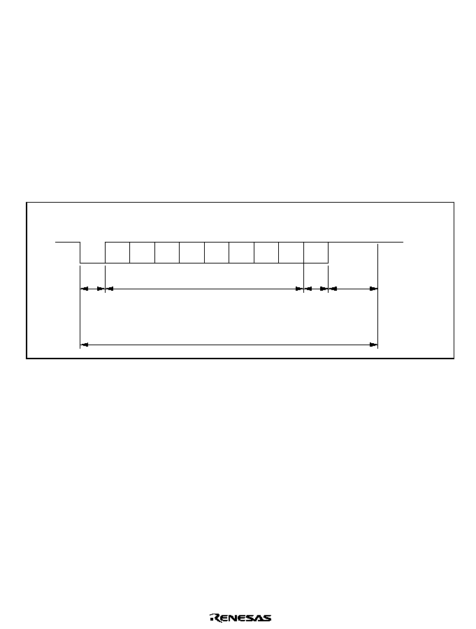
Rev. 2.0, 04/02, page 661 of 906
15.4
Operation in Asynchronous Mode
Figure 15.2 shows the general format for asynchronous serial communication. One frame consists
of a start bit (low level), followed by transfer data, a parity bit, and finally stop bits (high level). In
asynchronous serial communication, the transmission line is usually held in the mark state (high
level). The SCI monitors the transmission line, and when it goes to the space state (low level),
recognizes a start bit and starts serial communication. In asynchronous serial communication, the
communication line is usually held in the mark state (high level). The SCI monitors the
communication line, and when it goes to the space state (low level), recognizes a start bit and
starts serial communication. Inside the SCI, the transmitter and receiver are independent units,
enabling full-duplex communication. Both the transmitter and the receiver also have a double-
buffered structure, so that data can be read or written during transmission or reception, enabling
continuous data transfer.
LSB
Start
bit
MSB
Idle state
(mark state)
Stop bit(s)
0
Transmit/receive data
D0
D1
D2
D3
D4
D5
D6
D7
0/1
1
1
1
1
Serial
data
Parity
bit
1 bit
1 or
2 bits
7 or 8 bits
1 bit,
or none
One unit of transfer data (character or frame)
Figure 15.2 Data Format in Asynchronous Communication
(Example with 8-Bit Data, Parity, Two Stop Bits)
15.4.1
Data Transfer Format
Table 15.10 shows the data transfer formats that can be used in asynchronous mode. Any of 12
transfer formats can be selected according to the SMR setting. For details on the multiprocessor
bit, refer to section 15.5, Multiprocessor Communication Function.
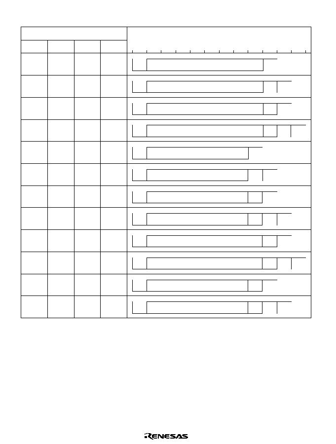
Rev. 2.0, 04/02, page 662 of 906
Table 15.10 Serial Transfer Formats (Asynchronous Mode)
PE
0
0
1
1
0
0
1
1
--
--
--
--
S
8-bit data
STOP
S
7-bit data
STOP
S
8-bit data
STOP STOP
S
8-bit data
P STOP
S
7-bit data
STOP
P
S
8-bit data
MPB STOP
S
8-bit data
MPB STOP STOP
S
7-bit data
STOP
MPB
S
7-bit data
STOP
MPB
STOP
S
7-bit data
STOP
STOP
CHR
0
0
0
0
1
1
1
1
0
0
1
1
MP
0
0
0
0
0
0
0
0
1
1
1
1
STOP
0
1
0
1
0
1
0
1
0
1
0
1
SMR Settings
1
2
3
4
5
6
7
8
9
10
11
12
Serial Transfer Format and Frame Length
STOP
S
8-bit data
P STOP
S
7-bit data
STOP
P
STOP
Legend
S
: Start bit
STOP : Stop bit
P
: Parity bit
MPB
: Multiprocessor bit
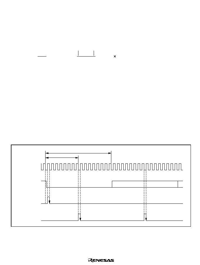
Rev. 2.0, 04/02, page 663 of 906
15.4.2
Receive Data Sampling Timing and Reception Margin in Asynchronous Mode
In asynchronous mode, the SCI operates on a basic clock with a frequency of 16 times the bit rate.
In reception, the SCI samples the falling edge of the start bit using the basic clock, and performs
internal synchronization. Receive data is latched at the middle of each bit by sampling the data at
the rising edge of the 8th pulse of the basic clock as shown in figure 15.3. Thus the reception
margin in asynchronous mode is given by formula (1) below.
M = { (0.5 ≠
) ≠ (L ≠ 0.5) F ≠
(1 + F) } 100 [%]
1
2N
D ≠ 0.5
N
... Formula (1)
Where
M: Reception Margin
N: Ratio of bit rate to clock (N = 16)
D: Clock duty cycle (D = 0.5 to 1.0)
L: Frame length (L = 9 to 12)
F: Absolute value of clock rate deviation
Assuming values of F = 0 and D = 0.5 in formula (1), a reception margin is given by formula
below.
M = {0.5 ≠ 1/(2
◊
16)}
◊
100 [%] = 46.875%
However, this is only the computed value, and a margin of 20% to 30% should be allowed in
system design.
Internal base
clock
16 clocks
8 clocks
Receive data
(RxD)
Synchronization
sampling timing
Start bit
D0
D1
Data sampling
timing
15 0
7
15 0
0
7
Figure 15.3 Receive Data Sampling Timing in Asynchronous Mode
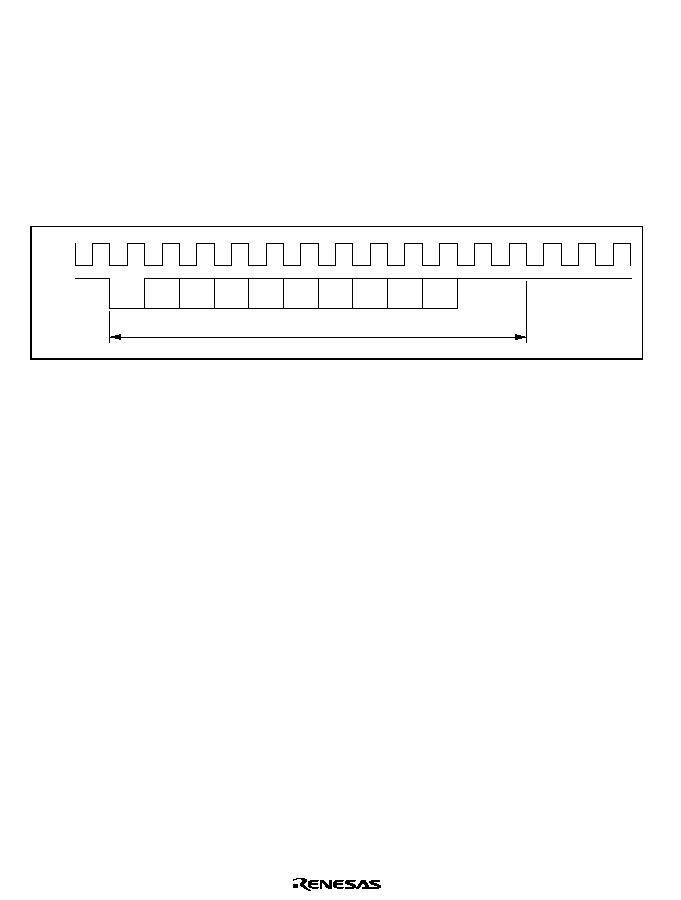
Rev. 2.0, 04/02, page 664 of 906
15.4.3
Clock
Either an internal clock generated by the on-chip baud rate generator or an external clock input at
the SCK pin can be selected as the SCI's serial clock, according to the setting of the C/
bit in
SMR and the CKE1 and CKE0 bits in SCR. When an external clock is input at the SCK pin, the
clock frequency should be 16 times the bit rate used.
When the SCI is operated on an internal clock, the clock can be output from the SCK pin. The
frequency of the clock output in this case is equal to the bit rate, and the phase is such that the
rising edge of the clock is in the middle of the transmit data, as shown in figure 15.4.
0
1 frame
SCK
TxD
D0
D1
D2
D3
D4
D5
D6
D7
0/1
1
1
Figure 15.4 Relation between Output Clock and Transfer Data Phase
(Asynchronous Mode)
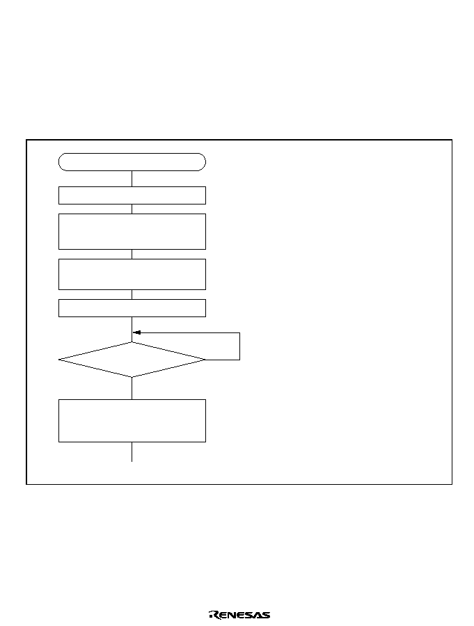
Rev. 2.0, 04/02, page 665 of 906
15.4.4
SCI Initialization (Asynchronous Mode)
Before transmitting and receiving data, you should first clear the TE and RE bits in SCR to 0, then
initialize the SCI as shown in figure 15.5. When the operating mode, transfer format, etc., is
changed, the TE and RE bits must be cleared to 0 before making the change. When the TE bit is
cleared to 0, the TDRE flag is set to 1. Note that clearing the RE bit to 0 does not initialize the
contents of the RDRF, PER, FER, and ORER flags, or the contents of RDR. When the external
clock is used in asynchronous mode, the clock must be supplied even during initialization.
Wait
<Initialization completed>
Start of initialization
Set data transfer format in
SMR and SCMR
[1]
Set CKE1 and CKE0 bits in SCR
(TE, RE bits 0)
No
Yes
Set value in BRR
Clear TE and RE bits in SCR to 0
[2]
[3]
Set TE and RE bits in
SCR to 1, and set RIE, TIE, TEIE,
and MPIE bits
[4]
1-bit interval elapsed?
[1] Set the clock selection in SCR.
Be sure to clear bits RIE, TIE,
TEIE, and MPIE, and bits TE and
RE, to 0.
When the clock is selected in
asynchronous mode, it is output
immediately after SCR settings are
made.
[2] Set the data transfer format in SMR
and SCMR.
[3] Write a value corresponding to the
bit rate to BRR. (Not necessary if
an external clock is used.)
[4] Wait at least one bit interval, then
set the TE bit or RE bit in SCR to 1.
Also set the RIE, TIE, TEIE, and
MPIE bits.
Setting the TE and RE bits enables
the TxD and RxD pins to be used.
Figure 15.5 Sample SCI Initialization Flowchart
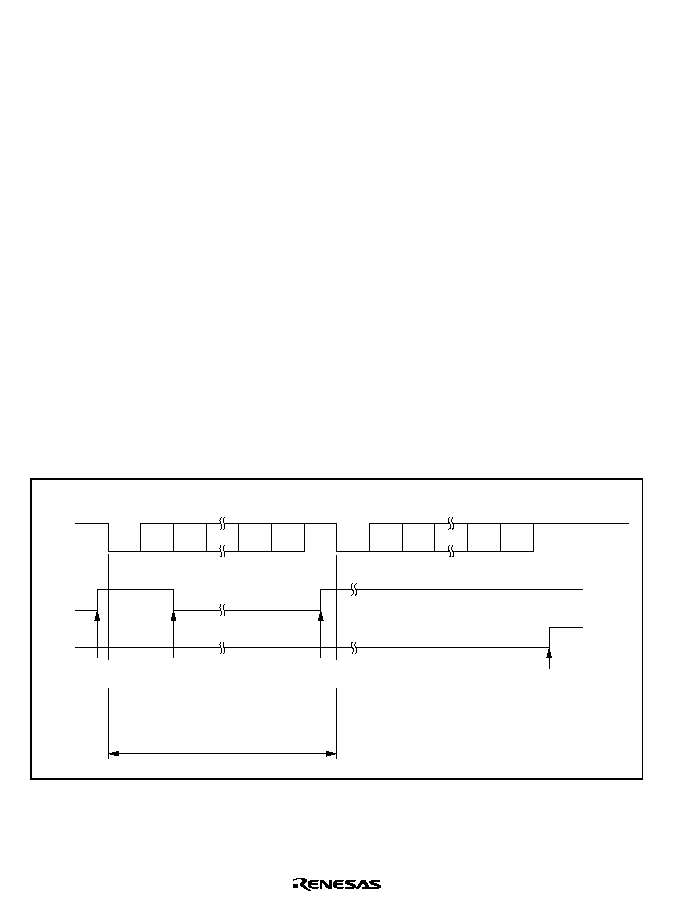
Rev. 2.0, 04/02, page 666 of 906
15.4.5
Data Transmission (Asynchronous Mode)
Figure 15.6 shows an example of the operation for transmission in asynchronous mode. In
transmission, the SCI operates as described below.
1. The SCI monitors the TDRE flag in SSR, and if is cleared to 0, recognizes that data has been
written to TDR, and transfers the data from TDR to TSR.
2. After transferring data from TDR to TSR, the SCI sets the TDRE flag to 1 and starts
transmission. If the TIE bit is set to 1 at this time, a transmit data empty interrupt request
(TXI) is generated. Because the TXI interrupt routine writes the next transmit data to TDR
before transmission of the current transmit data has finished, continuous transmission can be
enabled.
3. Data is sent from the TxD pin in the following order: start bit, transmit data, parity bit or
multiprocessor bit (may be omitted depending on the format), and stop bit.
4. The SCI checks the TDRE flag at the timing for sending the stop bit.
5. If the TDRE flag is 0, the data is transferred from TDR to TSR, the stop bit is sent, and then
serial transmission of the next frame is started.
6. If the TDRE flag is 1, the TEND flag in SSR is set to 1, the stop bit is sent, and then the "mark
state" is entered in which 1 is output. If the TEIE bit in SCR is set to 1 at this time, a TEI
interrupt request is generated.
Figure 15.7 shows a sample flowchart for transmission in asynchronous mode.
TDRE
TEND
0
1 frame
D0
D1
D7
0/1
1
0
D0
D1
D7
0/1
1
1
1
Data
Start
bit
Parity
bit
Stop
bit
Start
bit
Data Parity
bit
Stop
bit
TXI interrupt
request generated
Data written to TDR and
TDRE flag cleared to 0 in
TXI interrupt handling routine
TEI interrupt
request generated
Idle state
(mark state)
TXI interrupt
request generated
Figure 15.6 Example of Operation in Transmission in Asynchronous Mode
(Example with 8-Bit Data, Parity, One Stop Bit)
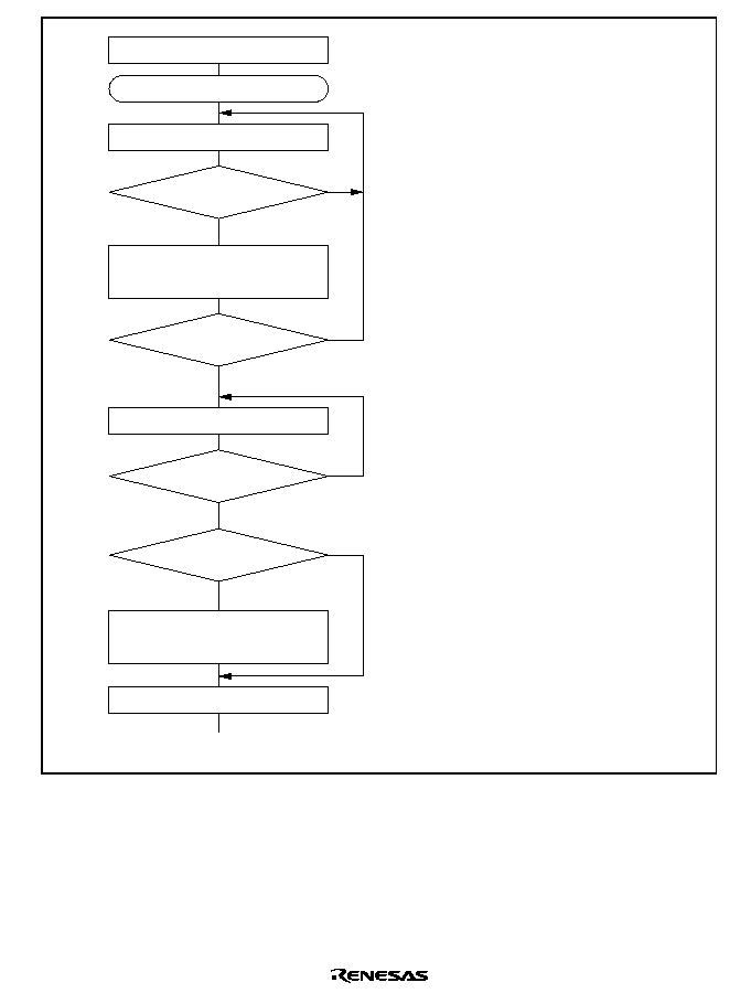
Rev. 2.0, 04/02, page 667 of 906
No
<End>
[1]
Yes
Initialization
Start of transmission
Read TDRE flag in SSR
[2]
Write transmit data to TDR
and clear TDRE flag in SSR to 0
No
Yes
No
Yes
Read TEND flag in SSR
[3]
No
Yes
[4]
Clear DR to 0 and
set DDR to 1
Clear TE bit in SCR to 0
TDRE = 1?
All data transmitted?
TEND = 1?
Break output?
[1] SCI initialization:
The TxD pin is automatically
designated as the transmit data
output pin.
After the TE bit is set to 1, a frame
of 1s is output, and transmission is
enabled.
[2] SCI status check and transmit data
write:
Read SSR and check that the
TDRE flag is set to 1, then write
transmit data to TDR and clear the
TDRE flag to 0.
[3] Serial transmission continuation
procedure:
To continue serial transmission,
read 1 from the TDRE flag to
confirm that writing is possible,
then write data to TDR, and then
clear the TDRE flag to 0. Checking
and clearing of the TDRE flag is
automatic when the DMAC or DTC
is activated by a transmit-data-
empty interrupt (TXI) request, and
data is written to TDR.
[4] Break output at the end of serial
transmission:
To output a break in serial
transmission, set DDR for the port
corresponding to the TxD pin to 1,
clear DR to 0, then clear the TE bit
in SCR to 0.
Figure 15.7 Sample Serial Transmission Flowchart
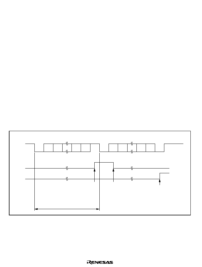
Rev. 2.0, 04/02, page 668 of 906
15.4.6
Serial Data Reception (Asynchronous Mode)
Figure 15.8 shows an example of the operation for reception in asynchronous mode. In serial
reception, the SCI operates as described below.
1. The SCI monitors the communication line, and if a start bit is detected, performs internal
synchronization, receives receive data in RSR, and checks the parity bit and stop bit.
2. If an overrun error (when reception of the next data is completed while the RDRF flag is still
set to 1) occurs, the ORER bit in SSR is set to 1. If the RIE bit in SCR is set to 1 at this time,
an ERI interrupt request is generated. Receive data is not transferred to RDR. The RDRF flag
remains to be set to 1.
3. If a parity error is detected, the PER bit in SSR is set to 1 and receive data is transferred to
RDR. If the RIE bit in SCR is set to 1 at this time, an ERI interrupt request is generated.
4. If a framing error (when the stop bit is 0) is detected, the FER bit in SSR is set to 1 and receive
data is transferred to RDR. If the RIE bit in SCR is set to 1 at this time, an ERI interrupt
request is generated.
5. If reception finishes successfully, the RDRF bit in SSR is set to 1, and receive data is
transferred to RDR. If the RIE bit in SCR is set to 1 at this time, an RXI interrupt request is
generated. Because the RXI interrupt routine reads the receive data transferred to RDR before
reception of the next receive data has finished, continuous reception can be enabled.
RDRF
FER
0
1 frame
D0
D1
D7
0/1
1
0
D0
D1
D7
0/1
0
1
1
Data
Start
bit
Parity
bit
Stop
bit
Start
bit
Data Parity
bit
Stop
bit
RXI interrupt
request
generated
ERI interrupt request
generated by framing
error
Idle state
(mark state)
RDR data read and RDRF
flag cleared to 0 in RXI
interrupt handling routine
Figure 15.8 Example of SCI Operation in Reception
(Example with 8-Bit Data, Parity, One Stop Bit)
Table 15.11 shows the states of the SSR status flags and receive data handling when a receive
error is detected. If a receive error is detected, the RDRF flag retains its state before receiving
data. Reception cannot be resumed while a receive error flag is set to 1. Accordingly, clear the

Rev. 2.0, 04/02, page 669 of 906
ORER, FER, PER, and RDRF bits to 0 before resuming reception. Figure 15.9 shows a sample
flowchart for serial data reception.
Table 15.11 SSR Status Flags and Receive Data Handling
SSR Status Flag
RDRF
*
ORER
FER
PER
Receive Data
Receive Error Type
1
1
0
0
Lost
Overrun error
0
0
1
0
Transferred to RDR
Framing error
0
0
0
1
Transferred to RDR
Parity error
1
1
1
0
Lost
Overrun error + framing error
1
1
0
1
Lost
Overrun error + parity error
0
0
1
1
Transferred to RDR
Framing error + parity error
1
1
1
1
Lost
Overrun error + framing error +
parity error
Note: The RDRF flag retains its state before data reception.
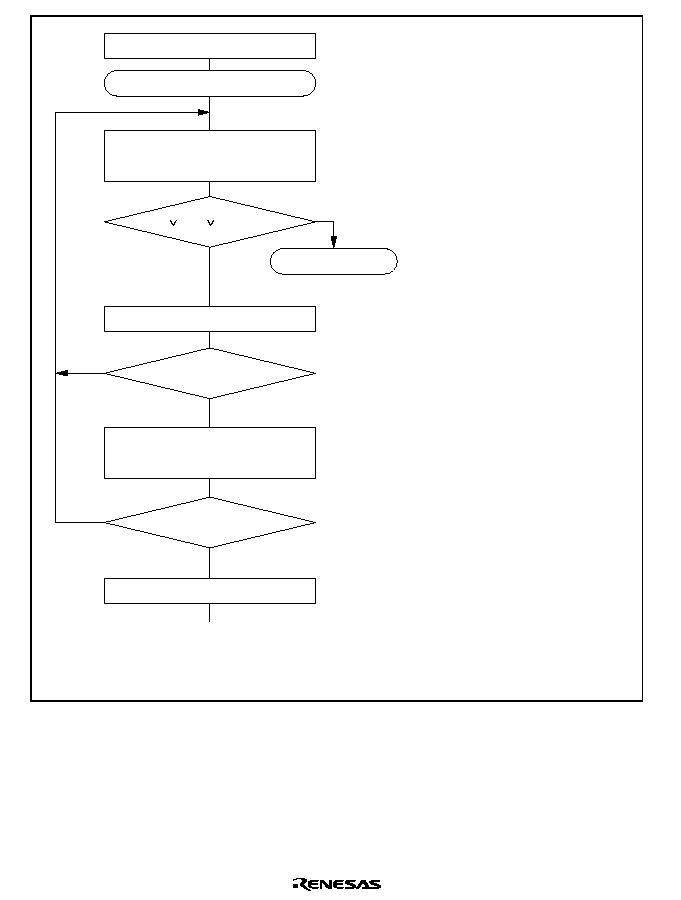
Rev. 2.0, 04/02, page 670 of 906
Yes
<End>
[1]
No
Initialization
Start of reception
[2]
No
Yes
Read RDRF flag in SSR
[4]
[5]
Clear RE bit in SCR to 0
Read ORER, PER, and
FER flags in SSR
Error handling
(Continued on next page)
[3]
Read receive data in RDR, and
clear RDRF flag in SSR to 0
No
Yes
PER
FER
ORER = 1?
RDRF = 1?
All data received?
SCI initialization:
The RxD pin is automatically
designated as the receive data
input pin.
Receive error handling and
break detection:
If a receive error occurs, read the
ORER, PER, and FER flags in
SSR to identify the error. After
performing the appropriate error
processing, ensure that the
ORER, PER, and FER flags are
all cleared to 0. Reception cannot
be resumed if any of these flags
are set to 1. In the case of a
framing error, a break can be
detected by reading the value of
the input port corresponding to
the RxD pin.
SCI status check and receive
data read :
Read SSR and check that RDRF
= 1, then read the receive data in
RDR and clear the RDRF flag to
0. Transition of the RDRF flag
from 0 to 1 can also be identified
by an RXI interrupt.
Serial reception continuation
procedure:
To continue serial reception,
before the stop bit for the current
frame is received, read the
RDRF flag, read RDR, and clear
the RDRF flag to 0. The RDRF
flag is cleared automatically
when the DMAC or DTC is
activated by an RXI interrupt and
the RDR value is read.
[1]
[2] [3]
[4]
[5]
Figure 15.9 Sample Serial Reception Data Flowchart (1)
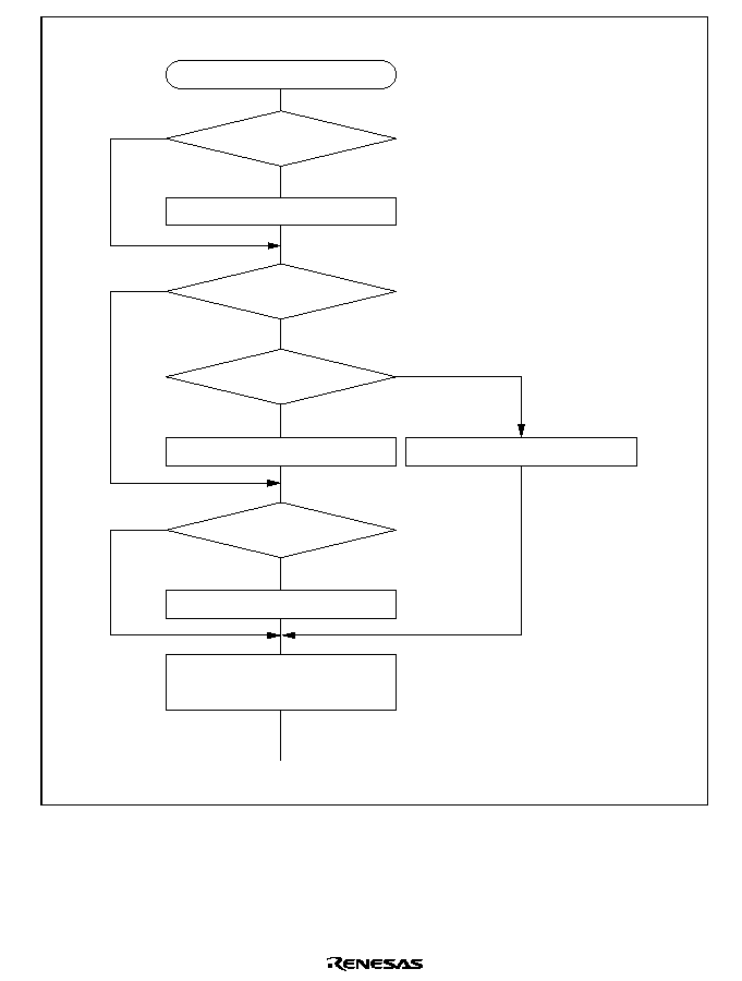
Rev. 2.0, 04/02, page 671 of 906
<End>
[3]
Error handling
Parity error handling
Yes
No
Clear ORER, PER, and
FER flags in SSR to 0
No
Yes
No
Yes
Framing error handling
No
Yes
Overrun error handling
ORER = 1?
FER = 1?
Break?
PER = 1?
Clear RE bit in SCR to 0
Figure 15.9 Sample Serial Reception Data Flowchart (2)

Rev. 2.0, 04/02, page 672 of 906
15.5
Multiprocessor Communication Function
Use of the multiprocessor communication function enables data transfer to be performed among a
number of processors sharing communication lines by means of asynchronous serial
communication using the multiprocessor format, in which a multiprocessor bit is added to the
transfer data. When multiprocessor communication is carried out, each receiving station is
addressed by a unique ID code. The serial communication cycle consists of two component
cycles: an ID transmission cycle which specifies the receiving station, and a data transmission
cycle to the specified receiving station. The multiprocessor bit is used to differentiate between the
ID transmission cycle and the data transmission cycle. If the multiprocessor bit is 1, the cycle is
an ID transmission cycle, and if the multiprocessor bit is 0, the cycle is a data transmission cycle.
Figure 15.10 shows an example of inter-processor communication using the multiprocessor
format. The transmitting station first sends communication data with a 1 multiprocessor bit added
to the ID code of the receiving station. It then sends transmit data as data with a 0 multiprocessor
bit added. When data with a 1 multiprocessor bit is received, the receiving station compares that
data with its own ID. The station whose ID matches then receives the data sent next. Stations
whose ID does not match continue to skip data until data with a 1 multiprocessor bit is again
received.
The SCI uses the MPIE bit in SCR to implement this function. When the MPIE bit is set to 1,
transfer of receive data from RSR to RDR, error flag detection, and setting the SSR status flags,
RDRF, FER, and ORER to 1 are inhibited until data with a 1 multiprocessor bit is received. On
reception of receive character with a 1 multiprocessor bit, the MPBR bit in SSR is set to 1 and the
MPIE bit is automatically cleared, thus normal reception is resumed. If the RIE bit in SCR is set to
1 at this time, an RXI interrupt is generated.
When the multiprocessor format is selected, the parity bit setting is invalid. All other bit settings
are the same as those in normal asynchronous mode. The clock used for multiprocessor
communication is the same as that in normal asynchronous mode.
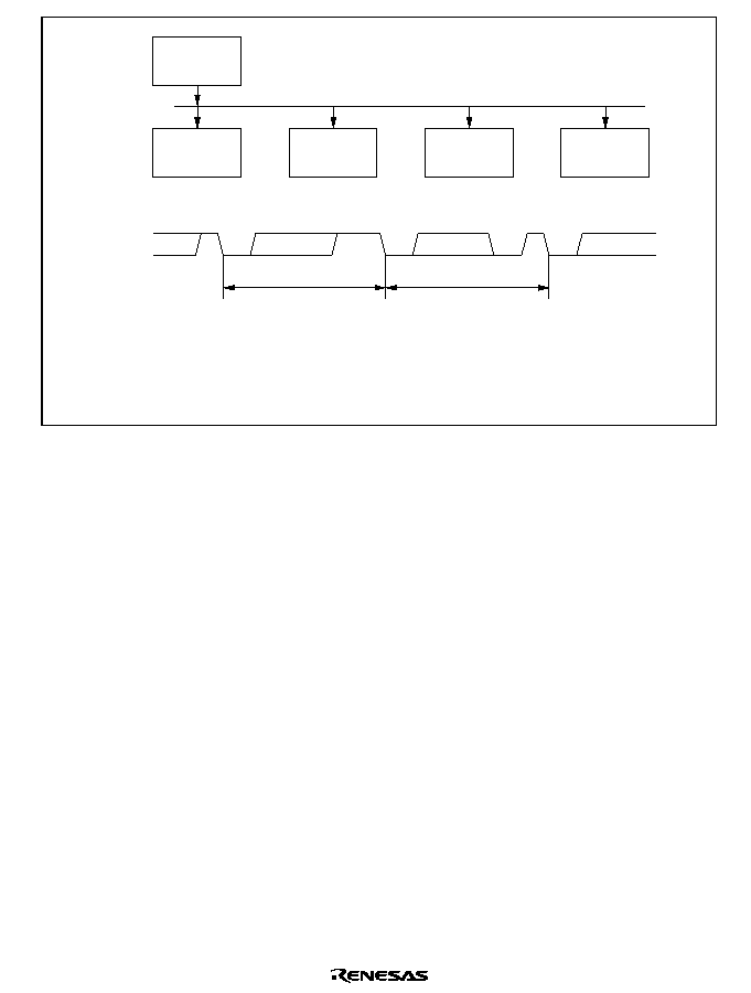
Rev. 2.0, 04/02, page 673 of 906
Transmitting
station
Receiving
station A
(ID = 01)
Receiving
station B
(ID = 02)
Receiving
station C
(ID = 03)
Receiving
station D
(ID = 04)
Serial communication line
Serial
data
ID transmission cycle =
receiving station
specification
Data transmission cycle =
data transmission to
receiving station specified by ID
(MPB= 1)
(MPB= 0)
H'01
H'AA
Legend
MPB: Multiprocessor bit
Figure 15.10 Example of Communication Using Multiprocessor Format
(Transmission of Data H'AA to Receiving Station A)

Rev. 2.0, 04/02, page 674 of 906
15.5.1
Multiprocessor Serial Data Transmission
Figure 15.11 shows a sample flowchart for multiprocessor serial data transmission. For an ID
transmission cycle, set the MPBT bit in SSR to 1 before transmission. For a data transmission
cycle, clear the MPBT bit in SSR to 0 before transmission. All other SCI operations are the same
as those in asynchronous mode.

Rev. 2.0, 04/02, page 675 of 906
No
<End>
[1]
Yes
Initialization
Start of transmission
Read TDRE flag in SSR
[2]
Write transmit data to TDR and
set MPBT bit in SSR
No
Yes
No
Yes
Read TEND flag in SSR
[3]
No
Yes
[4]
Clear DR to 0 and set DDR to 1
Clear TE bit in SCR to 0
TDRE = 1?
All data transmitted?
TEND = 1?
Break output?
Clear TDRE flag to 0
SCI initialization:
The TxD pin is automatically
designated as the transmit data
output pin.
After the TE bit is set to 1,
a frame of 1s is output, and
transmission is enabled.
SCI status check and transmit
data write:
Read SSR and check that the
TDRE flag is set to 1, then write
transmit data to TDR. Set the
MPBT bit in SSR to 0 or 1.
Finally, clear the TDRE flag to 0.
Serial transmission continuation
procedure:
To continue serial transmission,
be sure to read 1 from the TDRE
flag to confirm that writing is
possible, then write data to TDR,
and then clear the TDRE flag to
0. Checking and clearing of the
TDRE flag is automatic when the
DMAC or DTC is activated by a
transmit-data-empty interrupt
(TXI) request, and data is written
to TDR.
Break output at the end of serial
transmission:
To output a break in serial
transmission, set the port DDR to
1, clear DR to 0, then clear the
TE bit in SCR to 0.
[1]
[2]
[3]
[4]
Figure 15.11 Sample Multiprocessor Serial Transmission Flowchart
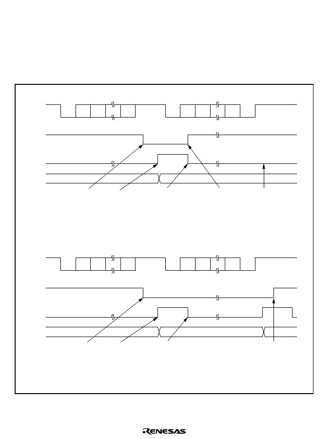
Rev. 2.0, 04/02, page 676 of 906
15.5.2
Multiprocessor Serial Data Reception
Figure 15.13 shows a sample flowchart for multiprocessor serial data reception. If the MPIE bit in
SCR is set to 1, data is skipped until data with a 1 multiprocessor bit is received. On receiving
data with a 1 multiprocessor bit, the receive data is transferred to RDR. An RXI interrupt request
is generated at this time. All other SCI operations are the same as in asynchronous mode. Figure
15.12 shows an example of SCI operation for multiprocessor format reception.
MPIE
RDR
value
0
D0
D1
D7
1
1
0
D0
D1
D7
0
1
1
1
Data (ID1)
Start
bit
MPB
Stop
bit
Start
bit
Data (Data1)
MPB
Stop
bit
RXI interrupt
request
(multiprocessor
interrupt)
generated
MPIE = 0
Idle state
(mark state)
RDRF
RDR data read
and RDRF flag
cleared to 0 in
RXI interrupt
handling routine
If not this station's ID,
MPIE bit is set to 1
again
RXI interrupt request is
not generated, and RDR
retains its state
ID1
(a) Data does not match station's ID
MPIE
RDR
value
0
D0
D1
D7
1
1
0
D0
D1
D7
0
1
1
1
Data (ID2)
Start
bit
MPB
Stop
bit
Start
bit
Data (Data2)
MPB
Stop
bit
RXI interrupt
request
(multiprocessor
interrupt)
generated
MPIE = 0
Idle state
(mark state)
RDRF
RDR data read and
RDRF flag cleared
to 0 in RXI interrupt
handling routine
Matches this station's ID,
so reception continues, and
data is received in RXI
interrupt handling routine
MPIE bit set to 1
again
ID2
(b) Data matches station's ID
Data2
ID1
Figure 15.12 Example of SCI Operation in Reception
(Example with 8-Bit Data, Multiprocessor Bit, One Stop Bit)
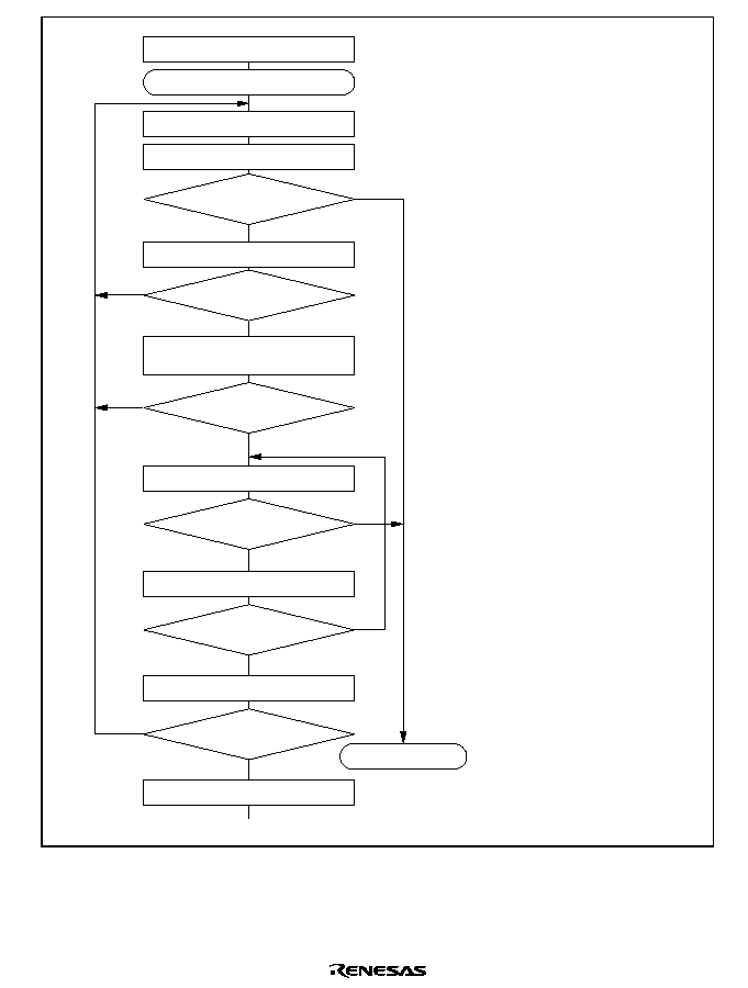
Rev. 2.0, 04/02, page 677 of 906
Yes
<End>
[1]
No
Initialization
Start of reception
No
Yes
[4]
Clear RE bit in SCR to 0
Error handling
(Continued on
next page)
[5]
No
Yes
FER
ORER = 1?
RDRF = 1?
All data received?
Set MPIE bit in SCR to 1
[2]
Read ORER and FER flags in SSR
Read RDRF flag in SSR
[3]
Read receive data in RDR
No
Yes
This station's ID?
Read ORER and FER flags in SSR
Yes
No
Read RDRF flag in SSR
No
Yes
FER
ORER = 1?
Read receive data in RDR
RDRF = 1?
SCI initialization:
The RxD pin is automatically
designated as the receive data
input pin.
ID reception cycle:
Set the MPIE bit in SCR to 1.
SCI status check, ID reception
and comparison:
Read SSR and check that the
RDRF flag is set to 1, then read
the receive data in RDR and
compare it with this station's ID.
If the data is not this station's ID,
set the MPIE bit to 1 again, and
clear the RDRF flag to 0.
If the data is this station's ID,
clear the RDRF flag to 0.
SCI status check and data
reception:
Read SSR and check that the
RDRF flag is set to 1, then read
the data in RDR.
Receive error handling and break
detection:
If a receive error occurs, read the
ORER and FER flags in SSR to
identify the error. After
performing the appropriate error
handling, ensure that the ORER
and FER flags are both cleared
to 0.
Reception cannot be resumed if
either of these flags is set to 1.
In the case of a framing error, a
break can be detected by reading
the RxD pin value.
[1]
[2]
[3]
[4]
[5]
Figure 15.13 Sample Multiprocessor Serial Reception Flowchart (1)
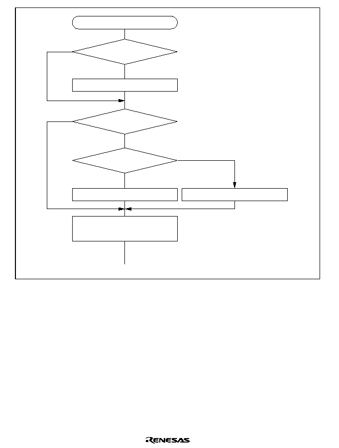
Rev. 2.0, 04/02, page 678 of 906
<End>
Error handling
Yes
No
Clear ORER, PER, and
FER flags in SSR to 0
No
Yes
No
Yes
Framing error handling
Overrun error handling
ORER = 1?
FER = 1?
Break?
Clear RE bit in SCR to 0
[5]
Figure 15.13 Sample Multiprocessor Serial Reception Flowchart (2)
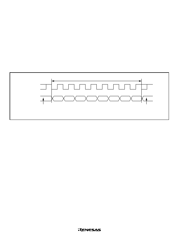
Rev. 2.0, 04/02, page 679 of 906
15.6
Operation in Clocked Synchronous Mode
Figure 15.14 shows the general format for clocked synchronous communication. In clocked
synchronous mode, data is transmitted or received in synchronization with clock pulses. One
character of communication data consists of 8-bit data. In clocked synchronous serial
communication, data on the transmission line is output from one falling edge of the serial clock to
the next. In clocked synchronous mode, the SCI receives data in synchronization with the rising
edge of the serial clock. After 8-bit data is output, the transmission line holds the MSB state. In
clocked synchronous mode, no parity or multiprocessor bit is added. Inside the SCI, the
transmitter and receiver are independent units, enabling full-duplex communication by use of a
common clock. Both the transmitter and the receiver also have a double-buffered structure, so that
data can be read or written during transmission or reception, enabling continuous data transfer.
Don't care
Don't care
One unit of transfer data (character or frame)
Bit 0
Serial
data
Serial
clock
Bit 1
Bit 3
Bit 4
Bit 5
LSB
MSB
Bit 2
Bit 6
Bit 7
*
Note:
*
High except in continuous transfer
*
Figure 15.14 Data Format in Clocked Synchronous Communication (For LSB-First)
15.6.1
Clock
Either an internal clock generated by the on-chip baud rate generator or an external
synchronization clock input at the SCK pin can be selected, according to the setting of CKE1 and
CKE0 bits in SCR. When the SCI is operated on an internal clock, the serial clock is output from
the SCK pin. Eight serial clock pulses are output in the transfer of one character, and when no
transfer is performed the clock is fixed high.
Rev. 2.0, 04/02, page 680 of 906
15.6.2
SCI Initialization (Clocked Synchronous Mode)
Before transmitting and receiving data, you should first clear the TE and RE bits in SCR to 0, then
initialize the SCI as described in a sample flowchart in figure 15.15. When the operating mode,
transfer format, etc., is changed, the TE and RE bits must be cleared to 0 before making the
change. When the TE bit is cleared to 0, the TDRE flag is set to 1. Note that clearing the RE bit
to 0 does not change the contents of the RDRF, PER, FER, and ORER flags, or the contents of
RDR.
Wait
<Transfer start>
Start of initialization
Set data transfer format in
SMR and SCMR
No
Yes
Set value in BRR
Clear TE and RE bits in SCR to 0
[2]
[3]
Set TE and RE bits in SCR to 1, and
set RIE, TIE, TEIE, and MPIE bits
Note: In simultaneous transmit and receive operations, the TE and RE bits should
both be cleared to 0 or set to 1 simultaneously.
[4]
1-bit interval elapsed?
Set CKE1 and CKE0 bits in SCR
(TE, RE bits 0)
[1]
[1] Set the clock selection in SCR. Be sure
to clear bits RIE, TIE, TEIE, and MPIE,
TE and RE, to 0.
[2] Set the data transfer format in SMR
and SCMR.
[3] Write a value corresponding to the bit
rate to BRR. (Not necessary if an
external clock is used.)
[4] Wait at least one bit interval, then set
the TE and RE bits in SCR to 1.
Also set the RIE, TIE, TEIE, and MPIE
bits.
Setting the TE and RE bits enable the
TxD and RxD pins to be used.
Figure 15.15 Sample SCI Initialization Flowchart

Rev. 2.0, 04/02, page 681 of 906
15.6.3
Serial Data Transmission (Clocked Synchronous Mode)
Figure 15.16 shows an example of SCI operation for transmission in clocked synchronous mode.
In serial transmission, the SCI operates as described below.
1. The SCI monitors the TDRE flag in SSR, and if is 0, recognizes that data has been written to
TDR, and transfers the data from TDR to TSR.
2. After transferring data from TDR to TSR, the SCI sets the TDRE flag to 1 and starts
transmission. If the TIE bit in SCR is set to 1 at this time, a TXI interrupt request is generated.
Because the TXI interrupt routine writes the next transmit data to TDR before transmission of
the current transmit data has finished, continuous transmission can be enabled.
3. 8-bit data is sent from the TxD pin synchronized with the output clock when output clock
mode has been specified and synchronized with the input clock when use of an external clock
has been specified.
4. The SCI checks the TDRE flag at the timing for sending the MSB.
5. If the TDRE flag is cleared to 0, data is transferred from TDR to TSR, and serial transmission
of the next frame is started.
6. If the TDRE flag is set to 1, the TEND flag in SSR is set to 1, and the TxD pin maintains the
output state of the last bit. If the TEIE bit in SCR is set to 1 at this time, a TEI interrupt
request is generated. The SCK pin is fixed high.
Figure 15.17 shows a sample flowchart for serial data transmission. Even if the TDRE flag is
cleared to 0, transmission will not start while a receive error flag (ORER, FER, or PER) is set to 1.
Make sure to clear the receive error flags to 0 before starting transmission. Note that clearing the
RE bit to 0 does not clear the receive error flags.
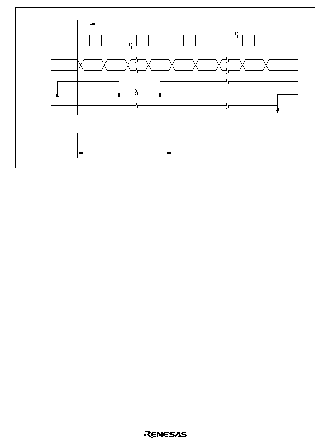
Rev. 2.0, 04/02, page 682 of 906
Transfer direction
Bit 0
Serial data
Serial clock
1 frame
TDRE
TEND
Bit 1
Bit 7
Bit 0
Bit 1
Bit 7
Bit 6
Data written to TDR
and TDRE flag
cleared to 0 in TXI
interrupt handling routine
TEI interrupt
request generated
TXI interrupt
request generated
TXI interrupt
request generated
Figure 15.16 Sample SCI Transmission Operation in Clocked Synchronous Mode
Rev. 2.0, 04/02, page 683 of 906
No
<End>
[1]
Yes
Initialization
Start of transmission
Read TDRE flag in SSR
[2]
Write transmit data to TDR and
clear TDRE flag in SSR to 0
No
Yes
No
Yes
Read TEND flag in SSR
[3]
Clear TE bit in SCR to 0
TDRE = 1?
All data transmitted?
TEND = 1?
[1] SCI initialization:
The TxD pin is automatically
designated as the transmit data output
pin.
[2] SCI status check and transmit data
write:
Read SSR and check that the TDRE
flag is set to 1, then write transmit data
to TDR and clear the TDRE flag to 0.
[3] Serial transmission continuation
procedure:
To continue serial transmission, be
sure to read 1 from the TDRE flag to
confirm that writing is possible, then
write data to TDR, and then clear the
TDRE flag to 0.
Checking and clearing of the TDRE
flag is automatic when the DMAC or
DTC is activated by a transmit-data-
empty interrupt (TXI) request and data
is written to TDR.
Figure 15.17 Sample Serial Transmission Flowchart
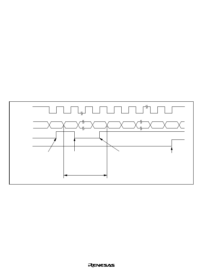
Rev. 2.0, 04/02, page 684 of 906
15.6.4
Serial Data Reception (Clocked Synchronous Mode)
Figure 15.18 shows an example of SCI operation for reception in clocked synchronous mode. In
serial reception, the SCI operates as described below.
1. The SCI performs internal initialization in synchronization with a synchronization clock input
or output, starts receiving data, and stores the received data in RSR.
2. If an overrun error (when reception of the next data is completed while the RDRF flag is still
set to 1) occurs, the ORER bit in SSR is set to 1. If the RIE bit in SCR is set to 1 at this time,
an ERI interrupt request is generated. Receive data is not transferred to RDR. The RDRF flag
remains to be set to 1.
3. If reception finishes successfully, the RDRF bit in SSR is set to 1, and receive data is
transferred to RDR. If the RIE bit in SCR is set to 1 at this time, an RXI interrupt request is
generated. Because the RXI interrupt routine reads the receive data transferred to RDR before
reception of the next receive data has finished, continuous reception can be enabled.
Bit 7
Serial
data
Serial
clock
1 frame
RDRF
ORER
Bit 0
Bit 7
Bit 0
Bit 1
Bit 6
Bit 7
RXI interrupt request
generated
RDR data read and
RDRF flag cleared to 0
in RXI interrupt handling
routine
RXI interrupt request
generated
ERI interrupt request
generated by overrun
error
Figure 15.18 Example of SCI Operation in Reception
Transfer cannot be resumed while a receive error flag is set to 1. Accordingly, clear the ORER,
FER, PER, and RDRF bits to 0 before resuming reception. Figure 15.19 shows a sample
flowchart for serial data reception.

Rev. 2.0, 04/02, page 685 of 906
Yes
<End>
[1]
No
Initialization
Start of reception
[2]
No
Yes
Read RDRF flag in SSR
[4]
[5]
Clear RE bit in SCR to 0
Error processing
(Continued below)
[3]
Read receive data in RDR, and
clear RDRF flag in SSR to 0
No
Yes
ORER = 1?
RDRF = 1?
All data received?
Read ORER flag in SSR
[1]
[2] [3]
[4]
[5]
SCI initialization:
The RxD pin is automatically
designated as the receive data
input pin.
Receive error handling:
If a receive error occurs, read the
ORER flag in SSR, and after
performing the appropriate error
handling, clear the ORER flag to
0. Transfer cannot be resumed if
the ORER flag is set to 1.
SCI status check and receive
data read:
Read SSR and check that the
RDRF flag is set to 1, then read
the receive data in RDR and
clear the RDRF flag to 0.
Transition of the RDRF flag from
0 to 1 can also be identified by
an RXI interrupt.
Serial reception continuation
procedure:
To continue serial reception,
before the MSB (bit 7) of the
current frame is received, finish
reading the RDRF flag, reading
RDR, and clearing the RDRF flag
to 0. The RDRF flag is cleared
automatically when the DMAC or
DTC is activated by a receive-
data-full interrupt (RXI) request
and the RDR value is read.
<End>
Error handling
Overrun error handling
[3]
Clear ORER flag in SSR to 0
Figure 15.19 Sample Serial Reception Flowchart

Rev. 2.0, 04/02, page 686 of 906
15.6.5
Simultaneous Serial Data Transmission and Reception (Clocked Synchronous
Mode)
Figure 15.20 shows a sample flowchart for simultaneous serial transmit and receive operations.
The following procedure should be used for simultaneous serial data transmit and receive
operations after the SCI is initialized. To switch from transmit mode to simultaneous transmit and
receive mode, after checking that the SCI has finished transmission and the TDRE and TEND
flags are set to 1, clear TE to 0. Then simultaneously set TE and RE to 1 with a single instruction.
To switch from receive mode to simultaneous transmit and receive mode, after checking that the
SCI has finished reception, clear RE to 0. Then after checking that the RDRF and receive error
flags (ORER, FER, and PER) are cleared to 0, simultaneously set TE and RE to 1 with a single
instruction.
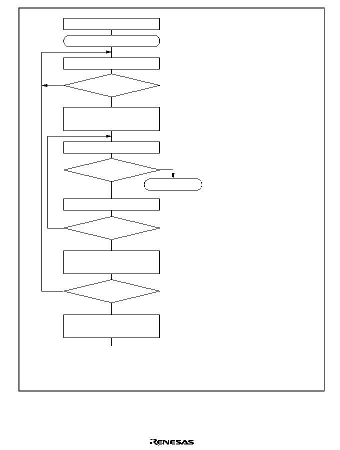
Rev. 2.0, 04/02, page 687 of 906
Yes
<End>
[1]
No
Initialization
Start of transmission/reception
[5]
Error handling
[3]
Read receive data in RDR, and
clear RDRF flag in SSR to 0
No
Yes
ORER = 1?
All data received?
[2]
Read TDRE flag in SSR
No
Yes
TDRE = 1?
Write transmit data to TDR and
clear TDRE flag in SSR to 0
No
Yes
RDRF = 1?
Read ORER flag in SSR
[4]
Read RDRF flag in SSR
Clear TE and RE bits in SCR to 0
Note: When switching from transmit or receive operation to simultaneous
transmit and receive operations, first clear the TE and RE bits to 0,
then set both these bits to 1 simultaneously.
[1]
[2]
[3]
[4]
[5]
SCI initialization:
The TxD pin is designated as the
transmit data output pin, and the
RxD pin is designated as the
receive data input pin, enabling
simultaneous transmit and receive
operations.
SCI status check and transmit data
write:
Read SSR and check that the
TDRE flag is set to 1, then write
transmit data to TDR and clear the
TDRE flag to 0.
Transition of the TDRE flag from 0 to
1 can also be identified by a TXI
interrupt.
Receive error handling:
If a receive error occurs, read the
ORER flag in SSR, and after
performing the appropriate error
handling, clear the ORER flag to 0.
Transmission/reception cannot be
resumed if the ORER flag is set to 1.
SCI status check and receive data
read:
Read SSR and check that the
RDRF flag is set to 1, then read the
receive data in RDR and clear the
RDRF flag to 0. Transition of the
RDRF flag from 0 to 1 can also be
identified by an RXI interrupt.
Serial transmission/reception
continuation procedure:
To continue serial transmission/
reception, before the MSB (bit 7) of
the current frame is received, finish
reading the RDRF flag, reading
RDR, and clearing the RDRF flag to
0. Also, before the MSB (bit 7) of
the current frame is transmitted,
read 1 from the TDRE flag to
confirm that writing is possible.
Then write data to TDR and clear
the TDRE flag to 0.
Checking and clearing of the TDRE
flag is automatic when the DMAC or
DTC is activated by a transmit-data-
empty interrupt (TXI) request and
data is written to TDR. Also, the
RDRF flag is cleared automatically
when the DMAC or DTC is activated
by a receive-data-full interrupt (RXI)
request and the RDR value is read.
Figure 15.20 Sample Flowchart of Simultaneous Serial Transmit and Receive Operations
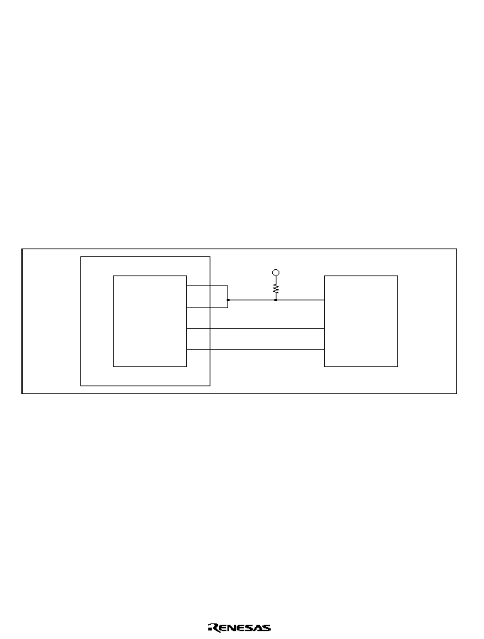
Rev. 2.0, 04/02, page 688 of 906
15.7
Operation in Smart Card Interface Mode
The SCI supports an IC card (Smart Card) interface conforming to ISO/IEC 7816-3 (Identification
Card) as a serial communication interface extension function. Switching between the normal
serial communication interface and the Smart Card interface is carried out by means of a register
setting.
15.7.1
Pin Connection Example
Figure 15.21 shows an example of connection with the Smart Card. In communication with an IC
card, since both transmission and reception are carried out on a single data transmission line, the
TxD pin and RxD pin should be connected with the LSI pin. The data transmission line should be
pulled up to the V
CC
power supply with a resistor. If an IC card is not connected, and the TE and
RE bits are both set to 1, closed transmission/reception is possible, enabling self-diagnosis to be
carried out. When the clock generated on the SCI is used by an IC card, the SCK pin output is
input to the CLK pin of the IC card. This LSI port output is used as the reset signal.
TxD
RxD
This LSI
V
CC
I/O
Connected equipment
IC card
Data line
CLK
RST
SCK
Rx (port)
Clock line
Reset line
Figure 15.21 Schematic Diagram of Smart Card Interface Pin Connections
15.7.2
Data Format (Except for Block Transfer Mode)
Figure 15.22 shows the transfer data format in Smart Card interface mode.
∑
One frame consists of 8-bit data plus a parity bit in asynchronous mode.
∑
In transmission, a guard time of at least 2 etu (Elementary Time Unit: the time for transfer of
one bit) is left between the end of the parity bit and the start of the next frame.
∑
If a parity error is detected during reception, a low error signal level is output for one etu
period, 10.5 etu after the start bit.
∑
If an error signal is sampled during transmission, the same data is retransmitted automatically
after the elapse of 2 etu or longer.
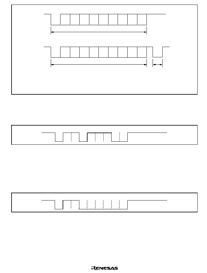
Rev. 2.0, 04/02, page 689 of 906
Ds
D0
D1
D2
D3
D4
D5
D6
D7
Dp
When there is no parity error
Transmitting station output
Ds
D0
D1
D2
D3
D4
D5
D6
D7
Dp
When a parity error occurs
Transmitting station output
DE
Receiving station
output
: Start bit
: Data bits
: Parity bit
: Error signal
Legend
Ds
D0 to D7
Dp
DE
Figure 15.22 Normal Smart Card Interface Data Format
Data transfer with the types of IC cards (direct convention and inverse convention) are performed
as described in the following.
Ds
A
Z
Z
A
Z
Z
Z
Z
A
A
(Z)
(Z)
State
D0
D1
D2
D3
D4
D5
D6
D7
Dp
Figure 15.23 Direct Convention (SDIR = SINV = O/
= 0)
As in the above sample start character, with the direct convention type, the logic 1 level
corresponds to state Z and the logic 0 level to state A, and transfer is performed in LSB-first order.
The start character data above is H'3B. For the direct convention type, clear the SDIR and SINV
bits in SCMR to 0. According to the Smart Card regulations, clear the O/
bit in SMR to 0 to
select even parity mode.
Ds
A
Z
Z
A
A
A
Z
A
A
A
(Z)
(Z)
State
D7
D6
D5
D4
D3
D2
D1
D0
Dp
Figure 15.24 Inverse Convention (SDIR = SINV = O/
= 1)
With the inverse convention type, the logic 1 level corresponds to state A and the logic 0 level to
state Z, and transfer is performed in MSB-first order. The start character data above is H'3F. For
the inverse convention type, set the SDIR and SINV bits in SCMR to 1. According to the Smart
Card regulations, even parity mode is the logic 0 level of the parity bit, and corresponds to state Z.
In this LSI, the SINV bit inverts only data bits D7 to D0. Therefore, set the O/
bit in SMR to 1
to invert the parity bit for both transmission and reception.

Rev. 2.0, 04/02, page 690 of 906
15.7.3
Block Transfer Mode
Operation in block transfer mode is the same as that in normal Smart Card interface, except for the
following points.
∑
In reception, though the parity check is performed, no error signal is output even if an error is
detected. However, the PER bit in SSR is set to 1 and must be cleared before receiving the
parity bit of the next frame.
∑
In transmission, a guard time of at least 1 etu is left between the end of the parity bit and the
start of the next frame.
∑
In transmission, because retransmission is not performed, the TEND flag is set to 1, 11.5 etu
after transmission start.
∑
As with the normal Smart Card interface, the ERS flag indicates the error signal status, but
since error signal transfer is not performed, this flag is always cleared to 0.
15.7.4
Receive Data Sampling Timing and Reception Margin
Only the internal clock generated by the on-chip baud rate generator is used as transmit/receive
clock in Smart Card interface. In Smart Card interface mode, the SCI operates on a basic clock
with a frequency of 32, 64, 372, or 256 times the bit rate (fixed at 16 times in normal
asynchronous mode) as determined by bits BCP1 and BCP0. In reception, the SCI samples the
falling edge of the start bit using the basic clock, and performs internal synchronization. As
shown in figure 15.25, by sampling receive data at the rising-edge of the 16th, 32nd, 186th, or
128th pulse of the basic clock, data can be latched at the middle of the bit. The reception margin is
given by the following formula.
M = | (0.5 ≠
) ≠ (L ≠ 0.5) F ≠
(1 + F) | 100%
1
2N
| D ≠ 0.5 |
N
Where
M: Reception margin (%)
N: Ratio of bit rate to clock (N = 32, 64, 372, and 256)
D: Clock duty cycle (D = 0 to 1.0)
L: Frame length (L = 10)
F: Absolute value of clock frequency deviation
Assuming values of F = 0, D = 0.5 and N = 372 in the above formula, the reception margin
formula is as follows.
M = (0.5 ≠ 1/2
◊
372)
◊
100%
= 49.866%

Rev. 2.0, 04/02, page 691 of 906
Internal
basic clock
372 clocks
186 clocks
Receive data
(RxD)
Synchronization
sampling timing
D0
D1
Data sampling
timing
185
371 0
371
185
0
0
Start bit
Figure 15.25 Receive Data Sampling Timing in Smart Card Mode
(Using Clock of 372 Times the Bit Rate)
15.7.5
Initialization
Before transmitting and receiving data, initialize the SCI as described below. Initialization is also
necessary when switching from transmit mode to receive mode, or vice versa.
1. Clear the TE and RE bits in SCR to 0.
2. Clear the error flags ERS, PER, and ORER in SSR to 0.
3. Set the GM, BLK, O/
, BCP1, BCP0, CKS1, and CKS0 bits in SMR. Set the PE bit to 1.
4. Set the SMIF, SDIR, and SINV bits in SCMR.
When the SMIF bit is set to 1, the TxD and RxD pins are both switched from ports to SCI pins,
and are placed in the high-impedance state.
5. Set the value corresponding to the bit rate in BRR.
6. Set the CKE0 and CKE1 bits in SCR. Clear the TIE, RIE, TE, RE, MPIE, and TEIE bits to 0.
If the CKE0 bit is set to 1, the clock is output from the SCK pin.
7. Wait at least one bit interval, then set the TIE, RIE, TE, and RE bits in SCR. Do not set the TE
bit and RE bit at the same time, except for self-diagnosis.
To switch from receive mode to transmit mode, after checking that the SCI has finished reception,
initialize the SCI, and clear RE to 0 and set TE to 1. Whether SCI has finished reception can be
checked with the RDRF, PER, or ORER flag. To switch from transmit mode to receive mode,
after checking that the SCI has finished transmission, initialize the SCI, and clear TE to 0 and set
RE to 1. Whether SCI has finished transmission can be checked with the TEND flag.

Rev. 2.0, 04/02, page 692 of 906
15.7.6
Data Transmission (Except for Block Transfer Mode)
As data transmission in Smart Card interface mode involves error signal sampling and
retransmission processing, the operations are different from those in normal serial communication
interface mode (except for block transfer mode). Figure 15.26 illustrates the retransfer operation
when the SCI is in transmit mode.
1. If an error signal is sampled from the receiving end after transmission of one frame is
completed, the ERS bit in SSR is set to 1. If the RIE bit in SCR is set at this time, an ERI
interrupt request is generated. The ERS bit in SSR should be cleared to 0 before the next
parity bit is sampled.
2. The TEND bit in SSR is not set for a frame for which an error signal is received. Data is
retransferred from TDR to TSR, and retransmitted automatically.
3. If an error signal is not sent back from the receiving end, the ERS bit in SSR is not set.
Transmission of one frame, including a retransfer, is judged to have been completed, and the
TEND bit in SSR is set to 1. If the TIE bit in SCR is set at this time, a TXI interrupt request is
generated. Writing transmit data to TDR transfers the next transmit data.
Figure 15.28 shows a flowchart for transmission. The sequence of transmit operations can be
performed automatically by specifying the DTC or DMAC to be activated with a TXI interrupt
source. In a transmit operation, the TDRE flag is also set to 1 at the same time as the TEND flag in
SSR, and a TXI interrupt will be generated if the TIE bit in SCR has been set to 1. If the TXI
request is designated beforehand as a DTC or DMAC activation source, the DTC or DMAC will
be activated by the TXI request, and transfer of the transmit data will be carried out. The TDRE
and TEND flags are automatically cleared to 0 when data transfer is performed by the DTC or
DMAC. In the event of an error, the SCI retransmits the same data automatically. During this
period, the TEND flag remains cleared to 0 and the DTC or DMAC is not activated. Therefore,
the SCI and DTC or DMAC will automatically transmit the specified number of bytes in the event
of an error, including retransmission. However, the ERS flag is not cleared automatically when an
error occurs, and so the RIE bit should be set to 1 beforehand so that an ERI request will be
generated in the event of an error, and the ERS flag will be cleared.
When performing transfer using the DTC or DMAC, it is essential to set and enable the DTC or
DMAC before carrying out SCI setting. For details on the DTC or DMAC setting procedures,
refer to section 9, Data Transfer Controller (DTC) or section 7, DMA Controller (DMAC).
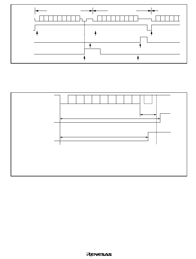
Rev. 2.0, 04/02, page 693 of 906
D0 D1 D2 D3 D4 D5 D6 D7 Dp
DE
Ds D0 D1 D2 D3 D4 D5 D6 D7 Dp
(DE)
Ds D0 D1 D2 D3 D4
Ds
Transfer
frame n+1
Retransferred frame
nth transfer frame
TDRE
TEND
[6]
FER/ERS
Transfer to TSR from TDR
Transfer to TSR from TDR
Transfer to TSR
from TDR
[7]
[9]
[8]
Figure 15.26 Retransfer Operation in SCI Transmit Mode
The timing for setting the TEND flag depends on the value of the GM bit in SMR. The TEND
flag generation timing is shown in figure 15.27.
Ds
D0
D1
D2
D3
D4
D5
D6
D7
Dp
I/O data
12.5etu
TXI
(TEND interrupt)
11.0etu
DE
Guard
time
When GM = 0
When GM = 1
: Start bit
: Data bits
: Parity bit
: Error signal
Legend
Ds
D0 to D7
Dp
DE
Figure 15.27 TEND Flag Generation Timing in Transmission Operation
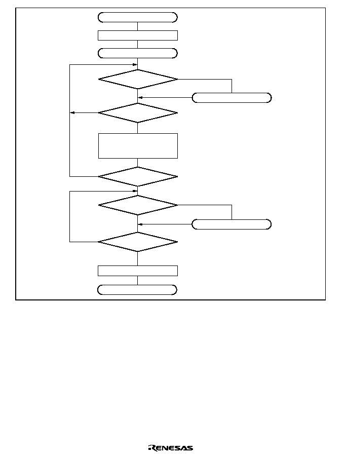
Rev. 2.0, 04/02, page 694 of 906
Initialization
No
Yes
Clear TE bit to 0
Start transmission
Start
No
No
No
Yes
Yes
Yes
Yes
No
End
Write data to TDR,
and clear TDRE flag
in SSR to 0
Error processing
Error processing
TEND = 1?
All data transmitted ?
TEND = 1?
ERS = 0?
ERS = 0?
Figure 15.28 Example of Transmission Processing Flow
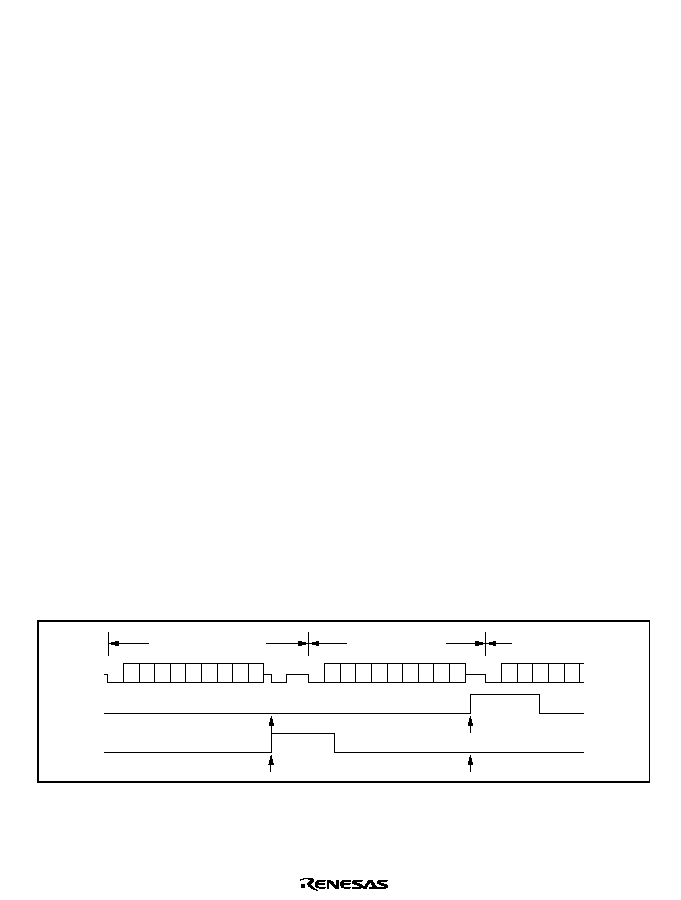
Rev. 2.0, 04/02, page 695 of 906
15.7.7
Serial Data Reception (Except for Block Transfer Mode)
Data reception in Smart Card interface mode uses the same operation procedure as for normal
serial communication interface mode. Figure 15.29 illustrates the retransfer operation when the
SCI is in receive mode.
1. If an error is found when the received parity bit is checked, the PER bit in SSR is
automatically set to 1. If the RIE bit in SCR is set at this time, an ERI interrupt request is
generated. The PER bit in SSR should be cleared to 0 before the next parity bit is sampled.
2. The RDRF bit in SSR is not set for a frame in which an error has occurred.
3. If no error is found when the received parity bit is checked, the PER bit in SSR is not set to 1.
The receive operation is judged to have been completed normally, and the RDRF flag in SSR
is automatically set to 1. If the RIE bit in SCR is set at this time, an RXI interrupt request is
generated.
Figure 15.30 shows a flowchart for reception. The sequence of receive operations can be
performed automatically by specifying the DTC or DMAC to be activated with an RXI interrupt
source. In a receive operation, an RXI interrupt request is generated when the RDRF flag in SSR
is set to 1. If the RXI request is designated beforehand as a DTC or DMAC activation source, the
DTC or DMAC will be activated by the RXI request, and transfer of the receive data will be
carried out. The RDRF flag is cleared to 0 automatically when data transfer is performed by the
DTC or DMAC. If an error occurs in receive mode and the ORER or PER flag is set to 1, a
transfer error interrupt (ERI) request will be generated, and so the error flag must be cleared to 0.
In the event of an error, the DTC or DMAC is not activated and receive data is skipped.
Therefore, receive data is transferred for only the specified number of bytes in the event of an
error. Even when a parity error occurs in receive mode and the PER flag is set to 1, the data that
has been received is transferred to RDR and can be read from there.
Note:
For details on receive operations in block transfer mode, refer to section 15.4, Operation in
Asynchronous Mode.
D0 D1 D2 D3 D4 D5 D6 D7 Dp DE
Ds D0 D1 D2 D3 D4 D5 D6 D7 Dp
(DE)
Ds D0 D1 D2 D3 D4
Ds
Transfer
frame n+1
Retransferred frame
nth transfer frame
RDRF
[1]
PER
[2]
[3]
[4]
Figure 15.29 Retransfer Operation in SCI Receive Mode
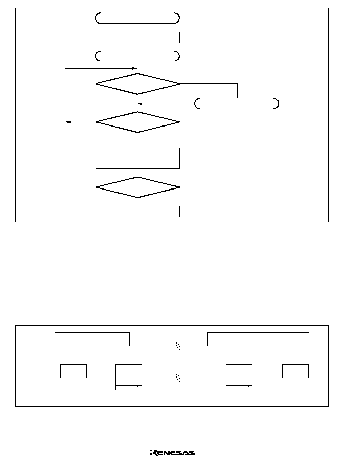
Rev. 2.0, 04/02, page 696 of 906
Initialization
Read RDR and clear
RDRF flag in SSR to 0
Clear RE bit to 0
Start reception
Start
Error processing
No
No
No
Yes
Yes
ORER = 0 and
PER = 0
RDRF = 1?
All data received?
Yes
Figure 15.30 Example of Reception Processing Flow
15.7.8
Clock Output Control
When the GM bit in SMR is set to 1, the clock output level can be fixed with bits CKE1 and
CKE0 in SCR. At this time, the minimum clock pulse width can be made the specified width.
Figure 15.31 shows the timing for fixing the clock output level. In this example, GM is set to 1,
CKE1 is cleared to 0, and the CKE0 bit is controlled.
Specified pulse width
SCK
CKE0
Specified pulse width
Figure 15.31 Timing for Fixing Clock Output Level
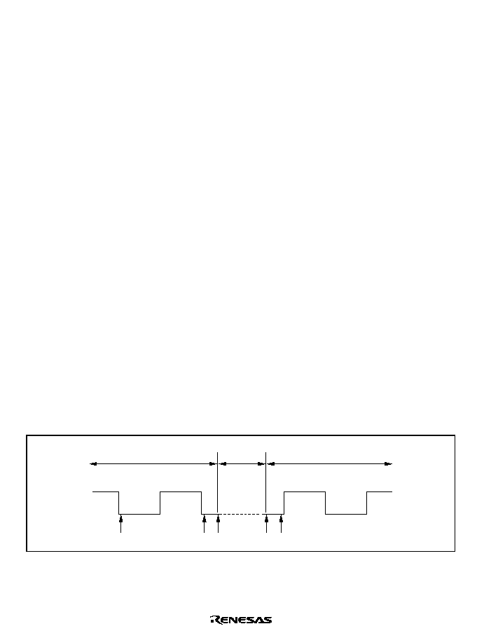
Rev. 2.0, 04/02, page 697 of 906
When turning on the power or switching between Smart Card interface mode and software standby
mode, the following procedures should be followed in order to maintain the clock duty cycle.
Powering On: To secure the clock duty cycle from power-on, the following switching procedure
should be followed.
1. The initial state is port input and high impedance. Use a pull-up resistor or pull-down
resistor to fix the potential.
2. Fix the SCK pin to the specified output level with the CKE1 bit in SCR.
3. Set SMR and SCMR, and switch to smart card mode operation.
4. Set the CKE0 bit in SCR to 1 to start clock output.
When changing from smart card interface mode to software standby mode:
1. Set the data register (DR) and data direction register (DDR) corresponding to the SCK pin
to the value for the fixed output state in software standby mode.
2. Write 0 to the TE bit and RE bit in the serial control register (SCR) to halt transmit/receive
operation. At the same time, set the CKE1 bit to the value for the fixed output state in
software standby mode.
3. Write 0 to the CKE0 bit in SCR to halt the clock.
4. Wait for one serial clock period.
During this interval, clock output is fixed at the specified level, with the duty cycle
preserved.
5. Make the transition to the software standby state.
When returning to smart card interface mode from software standby mode:
1. Exit the software standby state.
2. Write 1 to the CKE0 bit in SCR and output the clock. Signal generation is started with the
normal duty cycle.
[1] [2] [3]
[4] [5]
[7]
Software
standby
Normal operation
Normal operation
[6]
Figure 15.32 Clock Halt and Restart Procedure
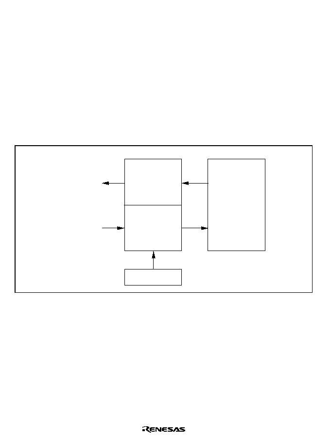
Rev. 2.0, 04/02, page 698 of 906
15.8
IrDA Operation
When the IrDA function is enabled with bit IrE in IrCR, the SCI_0 TxD0 and RxD0 signals are
subjected to waveform encoding/decoding conforming to IrDA specification version 1.0 (IrTxD
and IrRxD pins). By connecting these pins to an infrared transceiver/receiver, it is possible to
implement infrared transmission/reception conforming to the IrDA specification version 1.0
system.
In the IrDA specification version 1.0 system, communication is started at a transfer rate of 9600
bps, and subsequently the transfer rate can be varied as necessary. As the IrDA interface in this
LSI does not include a function for varying the transfer rate automatically, the transfer rate setting
must be changed by software.
Figure 15.33 shows a block diagram of the IrDA function.
IrDA
Pulse encoder
Pulse decoder
TxD0/IrTxD
RxD0/IrRxD
SCI0
TxD
RxD
IrCR
Figure 15.33 Block Diagram of IrDA
Transmission: In transmission, the output signal (UART frame) from the SCI is converted to an
IR frame by the IrDA interface (see figure 15.34).
When the serial data is 0, a high pulse of 3/16 the bit rate (interval equivalent to the width of one
bit) is output (initial value). The high-level pulse can be varied according to the setting of bits
IrCKS2 to IrCKS0 in IrCR.
In the specification, the high pulse width is fixed at a minimum of 1.41 µs, and a maximum of
(3/16 + 2.5%)
◊
bit rate or (3/16
◊
bit rate) + 1.08 µs. When system clock ¯ is 20 MHz, 1.6 µs can
be set for a high pulse width with a minimum value of 1.41 µs.

Rev. 2.0, 04/02, page 699 of 906
When the serial data is 1, no pulse is output.
UART frame
Data
IR frame
Data
0
0
0
0
0
1
1
1
1
1
0
0
0
0
0
1
1
1
1
1
Start
bit
Transmit
Receive
Stop
bit
Start
bit
Stop
bit
Bit
cycle
Pulse width
1.6
µ
s to 3/16 bit cycle
Figure 15.34 IrDA Transmit/Receive Operations
Reception: In reception, IR frame data is converted to a UART frame by the IrDA interface, and
input to the SCI.
When a high pulse is detected, 0 data is output, and if there is no pulse during a one-bit interval, 1
data is output. Note that a pulse shorter than the minimum pulse width of 1.41 µs will be identified
as a 0 signal.
High Pulse Width Selection: Table 15.12 shows possible settings for bits IrCKS2 to IrCKS0
(minimum pulse width), and operating frequencies of this LSI and bit rates, for making the pulse
width shorter than 3/16 times the bit rate in transmission.

Rev. 2.0, 04/02, page 700 of 906
Table 15.12 Settings of Bits IrCKS2 to IrCKS0
Operating
Bit Rate (bps) (Above) /Bit Period
◊
3/16 (µs) (Below)
Frequency
2400
9600
19200
38400
57600
115200
¯ (MHz)
78.13
19.53
9.77
4.88
3.26
1.63
2
010
010
010
010
010
--
2.097152
010
010
010
010
010
--
2.4576
010
010
010
010
010
--
3
011
011
011
011
011
--
3.6864
011
011
011
011
011
011
4.9152
011
011
011
011
011
011
5
011
011
011
011
011
011
6
100
100
100
100
100
100
6.144
100
100
100
100
100
100
7.3728
100
100
100
100
100
100
8
100
100
100
100
100
100
9.8304
100
100
100
100
100
100
10
100
100
100
100
100
100
12
101
101
101
101
101
101
12.288
101
101
101
101
101
101
14
101
101
101
101
101
101
14.7456
101
101
101
101
101
101
16
101
101
101
101
101
101
16.9344
101
101
101
101
101
101
17.2032
101
101
101
101
101
101
18
101
101
101
101
101
101
19.6608
101
101
101
101
101
101
20
101
101
101
101
101
101
25
110
110
110
110
110
110
Legend
--: A bit rate setting cannot be made on the SCI side.

Rev. 2.0, 04/02, page 701 of 906
15.9
Interrupt Sources
15.9.1
Interrupts in Normal Serial Communication Interface Mode
Table 15.13 shows the interrupt sources in normal serial communication interface mode. A
different interrupt vector is assigned to each interrupt source, and individual interrupt sources can
be enabled or disabled using the enable bits in SCR.
When the TDRE flag in SSR is set to 1, a TXI interrupt request is generated. When the TEND
flag in SSR is set to 1, a TEI interrupt request is generated. A TXI interrupt can activate the DTC
or DMAC to perform data transfer. The TDRE flag is cleared to 0 automatically when data
transfer is performed by the DTC or DMAC.
When the RDRF flag in SSR is set to 1, an RXI interrupt request is generated. When the ORER,
PER, or FER flag in SSR is set to 1, an ERI interrupt request is generated. An RXI interrupt
request can activate the DTC or DMAC to perform data transfer. The RDRF flag is cleared to 0
automatically when data transfer is performed by the DTC or DMAC.
A TEI interrupt is generated when the TEND flag is set to 1 while the TEIE bit is set to 1. If a TEI
interrupt and a TXI interrupt are generated simultaneously, the TXI interrupt has priority for
acceptance. However, note that if the TDRE and TEND flags are cleared simultaneously by the
TXI interrupt routine, the SCI cannot branch to the TEI interrupt routine later.
Table 15.13 SCI Interrupt Sources
Channel
Name
Interrupt Source
Interrupt Flag
DTC
Activation
DMAC
Activation
Priority
ERI0
Receive Error
ORER, FER, PER
Not possible
Not possible
High
RXI0
Receive Data Full
RDRF
Possible
Possible
TXI0
Transmit Data Empty
TDRE
Possible
Possible
0
TEI0
Transmission End
TEND
Not possible
Not possible
ERI1
Receive Error
ORER, FER, PER
Not possible
Not possible
RXI1
Receive Data Full
RDRF
Possible
Possible
TXI1
Transmit Data Empty
TDRE
Possible
Possible
1
TEI1
Transmission End
TEND
Not possible
Not possible
ERI2
Receive Error
ORER, FER, PER
Not possible
Not possible
RXI2
Receive Data Full
RDRF
Possible
Not possible
TXI2
Transmit Data Empty
TDRE
Possible
Not possible
2
TEI2
Transmission End
TEND
Not possible
Not possible
Low

Rev. 2.0, 04/02, page 702 of 906
15.9.2
Interrupts in Smart Card Interface Mode
Table 15.14 shows the interrupt sources in Smart Card interface mode. The transmit end interrupt
(TEI) request cannot be used in this mode.
Table 15.14 SCI Interrupt Sources
Channel
Name
Interrupt Source
Interrupt Flag
DTC
Activation
DMAC
Activation
Priority
ERI0
Receive Error, detection
ORER, PER, ERS
Not possible
Not possible
High
RXI0
Receive Data Full
RDRF
Possible
Possible
0
TXI0
Transmit Data Empty
TEND
Possible
Possible
ERI1
Receive Error, detection
ORER, PER, ERS
Not possible
Not possible
RXI1
Receive Data Full
RDRF
Possible
Possible
1
TXI1
Transmit Data Empty
TEND
Possible
Possible
ERI2
Receive Error, detection
ORER, PER, ERS
Not possible
Not possible
RXI2
Receive Data Full
RDRF
Possible
Not possible
2
TXI2
Transmit Data Empty
TEND
Possible
Not possible
Low
In Smart Card interface mode, as in normal serial communication interface mode, transfer can be
carried out using the DTC or DMAC. In transmit operations, the TDRE flag is also set to 1 at the
same time as the TEND flag in SSR, and a TXI interrupt is generated. If the TXI request is
designated beforehand as a DTC or DMAC activation source, the DTC or DMAC will be activated
by the TXI request, and transfer of the transmit data will be carried out. The TDRE and TEND
flags are automatically cleared to 0 when data transfer is performed by the DTC or DMAC. In the
event of an error, the SCI retransmits the same data automatically. During this period, the TEND
flag remains cleared to 0 and the DTC or DMAC is not activated. Therefore, the SCI and DTC or
DMAC will automatically transmit the specified number of bytes in the event of an error,
including retransmission. However, the ERS flag is not cleared automatically when an error
occurs, and so the RIE bit should be set to 1 beforehand so that an ERI request will be generated in
the event of an error, and the ERS flag will be cleared.
When performing transfer using the DTC or DMAC, it is essential to set and enable the DTC or
DMAC before carrying out SCI setting. For details on the DTC or DMAC setting procedures,
refer to section 9, Data Transfer Controller (DTC) or section 7, DMA Controller (DMAC).
In receive operations, an RXI interrupt request is generated when the RDRF flag in SSR is set to
1. If the RXI request is designated beforehand as a DTC or DMAC activation source, the DTC or
DMAC will be activated by the RXI request, and transfer of the receive data will be carried out.
The RDRF flag is cleared to 0 automatically when data transfer is performed by the DTC or
DMAC. If an error occurs, an error flag is set but the RDRF flag is not. Consequently, the DTC or

Rev. 2.0, 04/02, page 703 of 906
DMAC is not activated, but instead, an ERI interrupt request is sent to the CPU. Therefore, the
error flag should be cleared.
15.10
Usage Notes
15.10.1
Module Stop Mode Setting
SCI operation can be disabled or enabled using the module stop control register. The initial setting
is for SCI operation to be halted. Register access is enabled by clearing module stop mode. For
details, refer to section 22, Power-Down Modes.
15.10.2
Break Detection and Processing
When framing error detection is performed, a break can be detected by reading the RxD pin value
directly. In a break, the input from the RxD pin becomes all 0s, and so the FER flag is set, and the
PER flag may also be set. Note that, since the SCI continues the receive operation after receiving
a break, even if the FER flag is cleared to 0, it will be set to 1 again.
15.10.3
Mark State and Break Sending
When TE is 0, the TxD pin is used as an I/O port whose direction (input or output) and level are
determined by DR and DDR. This can be used to set the TxD pin to mark state or send a break
during serial data transmission. To maintain the communication line at mark state until TE is set
to 1, set both PCR and PDR to 1. Since TE is cleared to 0 at this point, the TxD pin becomes an
I/O port, and 1 is output from the TxD pin. To send a break during serial transmission, first set
PCR to 1 and clear PDR to 0, and then clear TE to 0. When TE is cleared to 0, the transmitter is
initialized regardless of the current transmission state, the TxD pin becomes an I/O port, and 0 is
output from the TxD pin.
15.10.4
Receive Error Flags and Transmit Operations (Clocked Synchronous Mode Only)
Transmission cannot be started when a receive error flag (ORER, PER, or FER) is set to 1, even if
the TDRE flag is cleared to 0. Be sure to clear the receive error flags to 0 before starting
transmission. Note also that receive error flags cannot be cleared to 0 even if the RE bit is cleared
to 0.
15.10.5
Relation between Writes to TDR and the TDRE Flag
The TDRE flag in SSR is a status flag that indicates that transmit data has been transferred from
TDR to TSR. When the SCI transfers data from TDR to TSR, the TDRE flag is set to 1.
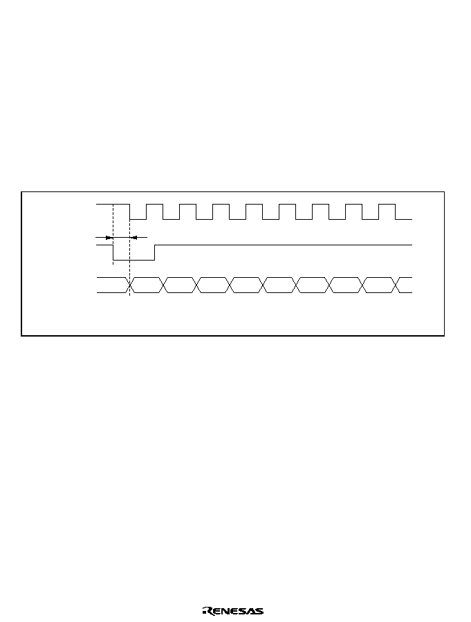
Rev. 2.0, 04/02, page 704 of 906
Data can be written to TDR regardless of the state of the TDRE flag. However, if new data is
written to TDR when the TDRE flag is cleared to 0, the data stored in TDR will be lost since it has
not yet been transferred to TSR. It is therefore essential to check that the TDRE flag is set to 1
before writing transmit data to TDR.
15.10.6
Restrictions on Use of DMAC or DTC
∑
When an external clock source is used as the serial clock, the transmit clock should not be
input until at least 5 ¯ clock cycles after TDR is updated by the DMAC or DTC. Misoperation
may occur if the transmit clock is input within 4 ¯ clocks after TDR is updated. (Figure 15.35)
∑
When RDR is read by the DMAC or DTC, be sure to set the activation source to the relevant
SCI receive-data-full interrupt (RXI).
t
D0
LSB
Serial data
SCK
D1
D3
D4
D5
D2
D6
D7
Note: When operating on an external clock, set t > 4 clocks.
TDRE
Figure 15.35 Example of Synchronous Transmission Using DTC
15.10.7
Operation in Case of Mode Transition
∑
Transmission
Operation should be stopped (by clearing TE, TIE, and TEIE to 0) before making a module
stop mode or software standby mode transition. TSR, TDR, and SSR are reset. The output pin
states in module stop mode or software standby mode depend on the port settings, and become
high-level output after the relevant mode is cleared. If a transition is made during
transmission, the data being transmitted will be undefined.
When transmitting without changing the transmit mode after the relevant mode is cleared,
transmission can be started by setting TE to 1 again, and performing the following sequence:
SSR read
TDR write
TDRE clearance. To transmit with a different transmit mode after
clearing the relevant mode, the procedure must be started again from initialization.
Figure 15.36 shows a sample flowchart for mode transition during transmission. Port pin states
during mode transition are shown in figures 15.37 and 15.38.

Rev. 2.0, 04/02, page 705 of 906
Operation should also be stopped (by clearing TE, TIE, and TEIE to 0) before making a
transition from transmission by DTC transfer to module stop mode or software standby mode
transition. To perform transmission with the DTC after the relevant mode is cleared, setting
TE and TIE to 1 will set the TXI flag and start DTC transmission.
∑
Reception
Receive operation should be stopped (by clearing RE to 0) before making a module stop mode
or software standby mode transition. RSR, RDR, and SSR are reset. If a transition is made
during reception, the data being received will be invalid.
To continue receiving without changing the reception mode after the relevant mode is cleared,
set RE to 1 before starting reception. To receive with a different receive mode, the procedure
must be started again from initialization.
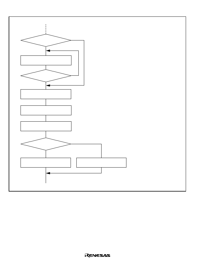
Rev. 2.0, 04/02, page 706 of 906
Figure 15.39 shows a sample flowchart for mode transition during reception.
Read TEND flag in SSR
TE = 0
Transition to software
standby mode
Exit from software
standby mode
Change
operating mode?
No
All data
transmitted?
TEND = 1
Yes
Yes
Yes
<Transmission>
No
No
[1]
[3]
[2]
TE = 1
Initialization
<Start of transmission>
[1]
Data being transmitted is interrupted.
After exiting software standby mode,
normal CPU transmission is possible
by setting TE to 1, reading SSR,
writing TDR, and clearing TDRE to 0,
but note that if the DTC has been
activated, the remaining data in
DTCRAM will be transmitted when
TE and TIE are set to 1.
[2]
If TIE and TEIE are set to 1, clear
them to 0 in the same way.
[3]
Includes module stop mode.
Figure 15.36 Sample Flowchart for Mode Transition during Transmission
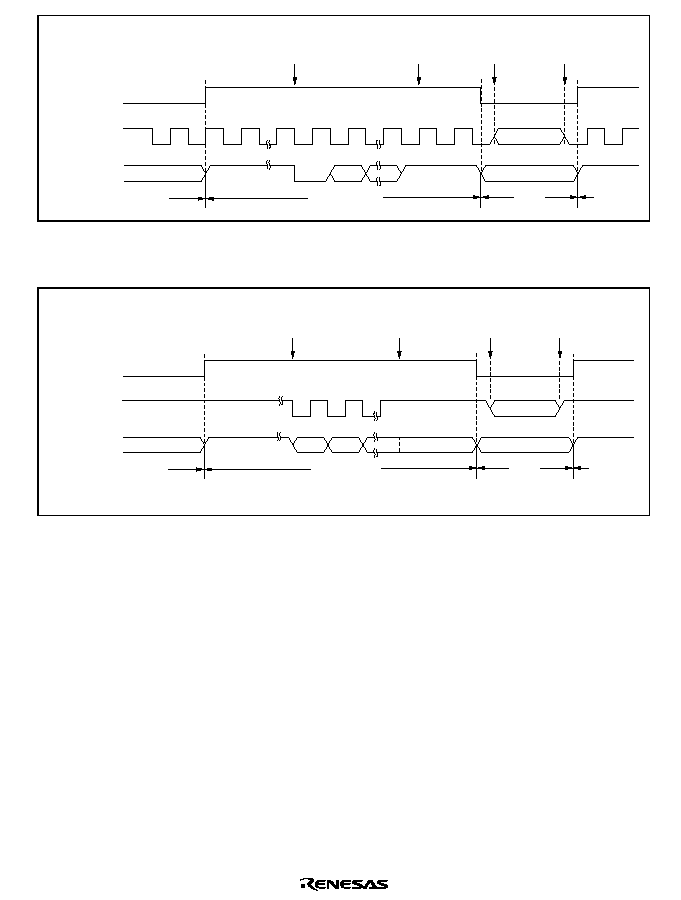
Rev. 2.0, 04/02, page 707 of 906
SCK output pin
TE bit
TxD output pin
Port input/output
High output
Port input/output
High output
Start
Stop
Start of transmission
End of
transmission
Port input/output
SCI TxD output
Port
SCI TxD
output
Port
Transition
to software
standby
Exit from
software
standby
Figure 15.37 Port Pin States during Mode Transition
(Internal Clock, Asynchronous Transmission)
Port input/output
Last TxD bit held
High output
*
Port input/output
Marking output
Port input/output
SCI TxD output
Port
Port
Note:
*
Initialized by software standby.
SCK output pin
TE bit
TxD output pin
SCI TxD
output
Start of transmission
End of
transmission
Transition
to software
standby
Exit from
software
standby
Figure 15.38 Port Pin States during Mode Transition
(Internal Clock, Synchronous Transmission)
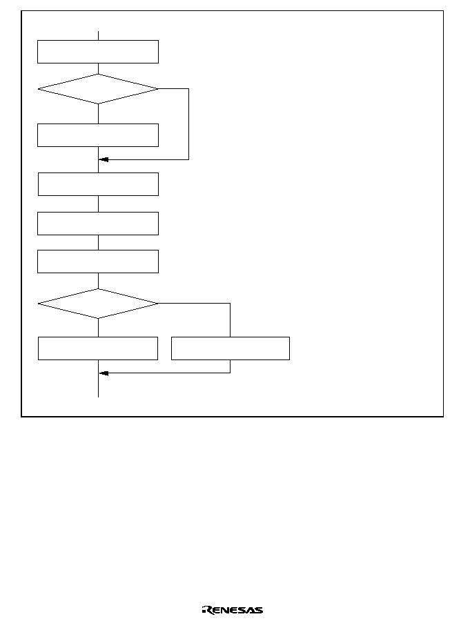
Rev. 2.0, 04/02, page 708 of 906
RE = 0
Transition to software
standby mode
Read receive data in RDR
Read RDRF flag in SSR
Exit from software
standby mode
Change
operating mode?
No
RDRF = 1
Yes
Yes
<Reception>
No
[1]
[2]
RE = 1
Initialization
<Start of reception>
[1]
Receive data being received
becomes invalid.
[2]
Includes module stop mode.
Figure 15.39 Sample Flowchart for Mode Transition during Reception

Rev. 2.0, 04/02, page 709 of 906
Section 16 A/D Converter
This LSI includes a successive approximation type 10-bit A/D converter that allows up to twelve
analog input channels to be selected. The block diagram of A/D converter is shown in figure 16.1.
16.1
Features
∑
10-bit resolution
∑
Twelve input channels
∑
Conversion time: 6.7 µs per channel (at 20 MHz operation)
∑
Two kinds of operating modes
Single mode: Single-channel A/D conversion
Scan mode: Continuous A/D conversion on 1 to 4 channels, or 1 to 8 channels (H8S/2678R
Series)
∑
Four data registers (H8S/2678 Series) or eight data registers (H8S/2678R Series)
Conversion results are held in a 16-bit data register for each channel
∑
Sample and hold function
∑
Three kinds of conversion start
Conversion can be started by software, 16-bit timer pulse unit (TPU), conversion start
trigger by 8-bit timer (TMR), or external trigger signal.
∑
Interrupt request
A/D conversion end interrupt (ADI) request can be generated
∑
Module stop mode can be set
ADCMS01A_010020020400

Rev. 2.0, 04/02, page 710 of 906
Module data bus
Control circuit
Internal data bus
10-bit D/A
Comparator
+
≠
Sample-and-
hold circuit
ADI interrupt
signal
Bus interface
A
D
C
S
R
A
D
C
R
A
D
D
R
D
A
D
D
R
C
A
D
D
R
G
A
D
D
R
F
A
D
D
R
E
A
D
D
R
H
A
D
D
R
B
A
D
D
R
A
AVCC
Vref
AVSS
AN0
AN1
AN2
AN3
AN4
AN5
AN6
AN7
AN12
AN13
AN14
AN15
Conversion start
trigger from 8-bit
timer or TPU
Successive approximations
register
Multiplexer
Legend
ADCR:
A/D control register
ADCSR: A/D control/status register
ADDRA: A/D data register A
ADDRB: A/D data register B
ADDRC: A/D data register C
Note:
*
Only in H8S/2678R series.
ADDRD: A/D data register D
ADDRE: A/D data register E
ADDRF: A/D data register F
ADDRG: A/D data register G
ADDRH: A/D data register H
*
*
*
*
Figure 16.1 Block Diagram of A/D Converter
16.2
Input/Output Pins
Table 16.1 shows the pin configuration of the A/D converter.
The twelve analog input pins are divided into two channel sets: channel set 0 (AN0 to AN7) and
channel set 1 (AN12 to AN15).

Rev. 2.0, 04/02, page 711 of 906
In the H8S/2678 Series, each channel set is divided into four channels
◊
two groups: group 0 in
channel set 0 (AN0 to AN3), group 1 in channel set 0 (AN4 to AN7), and group1 in channel set 1
(AN12 to AN15).
The AV
CC
and AV
SS
pins are the power supply pins for the analog block in the A/D converter. The
Vref pin is the A/D conversion reference voltage pin.
Table 16.1
A/D Converter Pins
Pin Name
Symbol
I/O
Function
Analog power supply pin
AV
CC
Input
Analog block power supply
Analog ground pin
AV
SS
Input
Analog block ground
Reference voltage pin
Vref
Input
A/D conversion reference voltage
Analog input pin 0
AN0
Input
Channel set 0 analog inputs
Analog input pin 1
AN1
Input
Analog input pin 2
AN2
Input
Analog input pin 3
AN3
Input
Analog input pin 4
AN4
Input
Analog input pin 5
AN5
Input
Analog input pin 6
AN6
Input
Analog input pin 7
AN7
Input
Analog input pin 12
AN12
Input
Channel set 1 analog inputs
Analog input pin 13
AN13
Input
Analog input pin 14
AN14
Input
Analog input pin 15
AN15
Input
A/D external trigger input
pin
$'75*
Input
External trigger input for starting A/D
conversion
16.3
Register Descriptions
The A/D converter has the following registers.
∑
A/D data register A (ADDRA)
∑
A/D data register B (ADDRB)
∑
A/D data register C (ADDRC)
∑
A/D data register D (ADDRD)
∑
A/D data register E (ADDRE)
∑
A/D data register F (ADDRF)
∑
A/D data register G (ADDRG)

Rev. 2.0, 04/02, page 712 of 906
∑
A/D data register H (ADDRH)
∑
A/D control/status register (ADCSR)
∑
A/D control register (ADCR)
16.3.1
A/D Data Registers A to H (ADDRA to ADDRH)
There are four 16-bit read-only ADDR registers, ADDRA to ADDRD (H8S/2678 Series) and
eight 16-bit read-only ADDR registers, ADDRA to ADDRH (H8S/2678R Series), used to store
the results of A/D conversion. The ADDR registers, which store a conversion result for each
channel, are shown in table 16.2.
The converted 10-bit data is stored to bits 15 to 6. The lower 6-bit data is always read as 0.
ADDR must not be accessed in 8-bit units and must be accessed in 16-bit units.
In the H8S/2678 Series, the data bus between the CPU and the A/D converter is 8-bit width. The
upper byte can be read directly from the CPU, but the lower byte should be read via a temporary
register. The temporary register contents are transferred from the ADDR when the upper byte data
is read. When reading the ADDR, read the only upper byte, or read in word unit.
In the H8S/2678R Series, the data bus between the CPU and the A/D converter is 16-bit width.
The data can be read directly from the CPU.
Table 16.2
Analog Input Channels and Corresponding ADDR Registers
∑
H8S/2678 Series
Analog Input Channel
Channel Set 0 (CH3 = 1)
Channel Set 1 (CH3 = 0)
Group 0
(CH2 = 0)
Group 1
(CH2 = 1)
Group 0
(CH2 = 0)
Group 1
(CH2 = 1)
A/D Data Register
which stores
conversion result
AN0
AN4
Setting prohibited
AN12
ADDRA
AN1
AN5
Setting prohibited
AN13
ADDRB
AN2
AN6
Setting prohibited
AN14
ADDRC
AN3
AN7
Setting prohibited
AN15
ADDRD

Rev. 2.0, 04/02, page 713 of 906
∑
H8S/2678R Series
Analog Input Channel
Channel Set 0 (CH3 = 0)
Channel Set 1 (CH3 = 1)
A/D Data Register which stores
conversion result
AN0
Nothing
ADDRA
AN1
Nothing
ADDRB
AN2
Nothing
ADDRC
AN3
Nothing
ADDRD
AN4
AN12
ADDRE
AN5
AN13
ADDRF
AN6
AN14
ADDRG
AN7
AN15
ADDRH
16.3.2
A/D Control/Status Register (ADCSR)
ADCSR controls A/D conversion operations.
∑
H8S/2678 Series
Bit
Bit Name
Initial Value
R/W
Description
7
ADF
0
R/(W)
*
A/D End Flag
A status flag that indicates the end of A/D
conversion.
[Setting conditions]
∑
When A/D conversion ends in single mode
∑
When A/D conversion ends on all specified
channels in scan mode
[Clearing conditions]
∑
When 0 is written after reading ADF = 1
∑
When the DTC or DMAC is activated by an
ADI interrupt and ADDR is read
6
ADIE
0
R/W
A/D Interrupt Enable
A/D conversion end interrupt (ADI) request
enabled when 1 is set

Rev. 2.0, 04/02, page 714 of 906
Bit
Bit Name
Initial Value
R/W
Description
5
ADST
0
R/W
A/D Start
Clearing this bit to 0 stops A/D conversion, and
the A/D converter enters wait state. When this bit
is set to 1 by software, TPU (trigger), TMR
(trigger), or the
$'75*
pin, A/D conversion starts.
This bit remains set to 1 during A/D conversion. In
single mode, cleared to 0 automatically when
conversion on the specified channel ends. In
scan mode, conversion continues sequentially on
the specified channels until this bit is cleared to 0
by a reset, or a transition to hardware standby
mode or software.
4
SCAN
0
R/W
Scan Mode
Selects single mode or scan mode as the A/D
conversion operating mode.
0: Single mode
1: Scan mode
3
CKS
0
R/W
Clock Select
Used together with the CKS1 bit in ADCR to set
the A/D conversion time.
When CKS1 = 0
0: 530 states (max)
1: 68 states (max)
When CKS = 1
0: 266 states (max)
1: 134 states (max)

Rev. 2.0, 04/02, page 715 of 906
Bit
Bit Name
Initial Value
R/W
Description
2
1
0
CH2
CH1
CH0
0
0
0
R/W
R/W
R/W
Channel Select 2 to 0
These bits are used together with the SCAN bit in
ADCSR and the CH3 bit in ADCR to select the
analog input channels.
When SCAN = 0,
When SCAN = 1,
CH3 = 0
CH3 = 0
0XXX: Setting prohibited 0XXX: Setting prohibited
100: AN12
100: AN12
101: AN13
101: AN12 and AN13
110: AN14
110: AN12 to AN14
111: AN15
111: AN12 to AN15
When SCAN = 0, When SCAN = 1,
CH3 = 1
CH3 = 1
000: AN0
000: AN0
001: AN1
001: AN0 and AN1
010: AN2
010: AN0 to AN2
011: AN3
011: AN0 to AN3
100: AN4
100: AN4
101: AN5
101: AN4 and AN5
110: AN6
110: AN4 to AN6
111: AN7
111: AN4 to AN7
Note:
Only 0 can be written in bit 7, to clear the flag.
Legend:
X: Don't care.

Rev. 2.0, 04/02, page 716 of 906
∑
H8S/2678R Series
Bit
Bit Name
Initial Value
R/W
Description
7
ADF
0
R/(W)
*
A/D End Flag
A status flag that indicates the end of A/D
conversion.
[Setting conditions]
∑
When A/D conversion ends in single mode
∑
When A/D conversion ends on all specified
channels in scan mode
[Clearing conditions]
∑
When 0 is written after reading ADF = 1
∑
When the DTC or DMAC is activated by an
ADI interrupt and ADDR is read
6
ADIE
0
R/W
A/D Interrupt Enable
A/D conversion end interrupt (ADI) request
enabled when 1 is set
5
ADST
0
R/W
A/D Start
Clearing this bit to 0 stops A/D conversion, and
the A/D converter enters wait state.
Setting this bit to 1 starts an A/D conversion. In
single mode, cleared to 0 automatically when
conversion on the specified channel ends. In
scan mode, conversion continues sequentially on
the specified channels until this bit is cleared to 0
by software, a reset, or a transition to software
standby mode, hardware standby mode or module
stop mode.
4
--
0
--
Reserved
This bit is always read as 0 and cannot be
modified.

Rev. 2.0, 04/02, page 717 of 906
Bit
Bit Name
Initial Value
R/W
Description
3
2
1
0
CH3
CH2
CH1
CH0
0
0
0
0
R/W
R/W
R/W
R/W
Channel select 3 to 0
Selects analog input together with bits SCANE
and SCANS in ADCR.
When SCANE = 0 and SCANS = X
0000: AN0
1000: Setting prohibited
0001: AN1
1001: Setting prohibited
0010: AN2
1010: Setting prohibited
0011: AN3
1011: Setting prohibited
0100: AN4
1100: AN12
0101: AN5
1101: AN13
0110: AN6
1110: AN14
0111: AN7
1111: AN15
When SCANE = 1 and SCANS = 0
0000: AN0
1000: Setting prohibited
0001: AN0 and AN1
1001: Setting prohibited
0010: AN0 to AN2
1010: Setting prohibited
0011: AN0 to AN3
1011: Setting prohibited
0100: AN4
1100: AN12
0101: AN4 and AN5
1101: AN12 and AN13
0110: AN4 to AN6
1110: AN12 to AN14
0111: AN4 to AN7
1111: AN12 to AN15
When SCANE = 1 and SCANS = 1
0000: AN0
1000: Setting prohibited
0001: AN0 and AN1
1001: Setting prohibited
0010: AN0 to AN2
1010: Setting prohibited
0011: AN0 to AN3
1011: Setting prohibited
0100: AN0 to AN4
1100: Setting prohibited
0101: AN0 to AN5
1101: Setting prohibited
0110: AN0 to AN6
1110: Setting prohibited
0111: AN0 to AN7
1111: Setting prohibited
Note:
Only 0 can be written in bit 7, to clear the flag.
Legend:
X: Don't care.

Rev. 2.0, 04/02, page 718 of 906
16.3.3
A/D Control Register (ADCR)
ADCR enables A/D conversion start by an external trigger input.
∑
H8S/2678 Series
Bit
Bit Name
Initial Value
R/W
Description
7
6
TRGS1
TRGS0
0
0
R/W
R/W
Timer Trigger Select 1 and 0:
These bits select enabling or disabling of the start
of A/D conversion by a trigger signal.
00: A/D conversion start by external trigger is
disabled
01: A/D conversion start by external trigger (TPU)
is enabled
10: A/D conversion start by external trigger (TMR)
is enabled
11: A/D conversion start by external trigger pin
(
$'75*
) is enabled
5
4
--
--
1
1
--
--
Reserved
These bits are always read as 1 and cannot be
modified.
3
CKS1
1
R/W
Clock Select 1
Used together with the CKS bit in ADCSR to set
the A/D conversion time. See the description of the
CKS bit for details.
2
CH3
1
R/W
Channel Select 3
Used together with bits CH2, CH1, and CH0 in
ADCSR to select the analog input channel(s). See
the description of bits CH2, CH1, and CH0 for
details.
1
0
--
--
1
1
--
--
Reserved
These bits are always read as 1 and cannot be
modified.

Rev. 2.0, 04/02, page 719 of 906
∑
H8S/2678R Series
Bit
Bit Name
Initial Value
R/W
Description
7
6
TRGS1
TRGS0
0
0
R/W
R/W
Timer Trigger Select 1 and 0
These bits select enabling or disabling of the start
of A/D conversion by a trigger signal.
00: A/D conversion start by external trigger is
disabled
01: A/D conversion start by external trigger (TPU)
is enabled
10: A/D conversion start by external trigger (TMR)
is enabled
11: A/D conversion start by external trigger pin
(
$'75*
) is enabled
5
4
SCANE
SCANS
0
0
R/W
R/W
Scan Mode
Selects single mode or scan mode as the A/D
conversion operating mode.
0x: Single mode
10: Scan mode. A/D conversion is performed
continuously for channels 1 to 4
11: Scan mode. A/D conversion is performed
continuously for channels 1 to 8.
3
2
CKS1
CKS0
0
0
R/W
R/W
Clock Select 1 to 0
Sets the A/D conversion time.
Only set bits CKS1 and CKS0 while conversion is
stopped (ADST = 0).
00: A/D conversion time = 530 states (max)
01: A/D conversion time = 266 states (max)
10: A/D conversion time = 134 states (max)
11: A/D conversion time = 68 states (max)
1
0
--
--
0
0
--
--
Reserved
These bits are always read as 0 and cannot be
modified.
Legend:
X: Don't care.

Rev. 2.0, 04/02, page 720 of 906
16.4
Operation
The A/D converter operates by successive approximation with 10-bit resolution. It has two
operating modes: single mode and scan mode. When changing the operating mode or analog input
channel, to prevent incorrect operation, first clear the bit ADST to 0 in ADCSR to halt A/D
conversion. The ADST bit can be set at the same time as the operating mode or analog input
channel is changed.
16.4.1
Single Mode
In single mode, A/D conversion is to be performed only once on the specified single channel.
Operations are as follows.
1. A/D conversion is started when the ADST bit in ADCSR is set to 1, according to the software
or external trigger input.
2. When A/D conversion is completed, the result is transferred to the corresponding A/D data
register to the channel.
3. On completion of conversion, the ADF bit in ADCSR is set to 1. If the ADIE bit is set to 1 at
this time, an ADI interrupt request is generated.
4. The ADST bit remains set to 1 during A/D conversion, and is automatically cleared to 0 when
conversion ends. When the ADST bit is cleared to 0 during A/D conversion, A/D conversion
stops and the A/D converter enters wait state.
16.4.2
Scan Mode
In scan mode, A/D conversion is to be performed sequentially on the specified channels:
maximum four channels or maximum eight channels (H8S/2678R Series). Operations are as
follows.
1. When the ADST bit in ADCSR is set to 1 by a software, TPU or external trigger input, A/D
conversion starts on the first channel in the group.
In the H8S/2678 Series, the A/D conversion starts on AN0 when CH3 and CH2 =10, AN4
when CH3 and CH2 = 11, or AN12 when CH3 and CH2 = 01.
In the H8S/2678R Series, the consecutive A/D conversion on maximum four channels
(SCANE and SCANS = 10) or on maximum eight channels (SCANE and SCANS = 11) can be
selected. When the consecutive A/D conversion is performed on the four channels, the A/D
conversion starts on AN0 when CH3 and CH2 =00, AN4 when CH3 and CH2 = 01, or AN12
when CH3 and CH2 = 11. When the consecutive A/D conversion is performed on the eight
channels, the A/D conversion starts on AN0 when SH3 and SH2 =00.
2. When A/D conversion for each channel is completed, the result is sequentially transferred to
the corresponding A/D data register to each channel.

Rev. 2.0, 04/02, page 721 of 906
3. When conversion of all the selected channels is completed, the ADF bit in ADCSR is set to 1.
If the ADIE bit is set to 1 at this time, an ADI interrupt is requested. Conversion of the first
channel in the group starts again.
4. The ADST bit is not cleared automatically, and steps [2] to [3] are repeated as long as the
ADST bit remains set to 1. When the ADST bit is cleared to 0, A/D conversion stops and the
A/D converter enters wait state. If the ADST bit is later set to 1, A/D conversion starts again
from the first channel in the group.
16.4.3
Input Sampling and A/D Conversion Time
The A/D converter has a built-in sample-and-hold circuit. The A/D converter samples the analog
input when A/D conversion start delay time (t
D
) passes after the ADST bit is set to 1, then starts
conversion. Figure 16.2 shows the A/D conversion timing. Table 16.3 indicates the A/D
conversion time.
As indicated in figure 16.2, the A/D conversion time (t
CONV
) includes t
D
and the input sampling time
(t
SPL
). The length of t
D
varies depending on the timing of the write access to ADCSR. The total
conversion time therefore varies within the ranges indicated in tables 16.3.
In scan mode, the values given in tables 16.3 apply to the first conversion time. The values given
in tables 16.4 apply to the second and subsequent conversions. The conversion time must be
within the ranges indicated in the descriptions, A/D Conversion Characteristics in section 24,
Electrical Characteristics. Therefore the CKS and CKS1 bits (H8S/2678 Series) or CKS1 and
CKS0 bits (H8S/2678R Series) must be set to satisfy this condition.
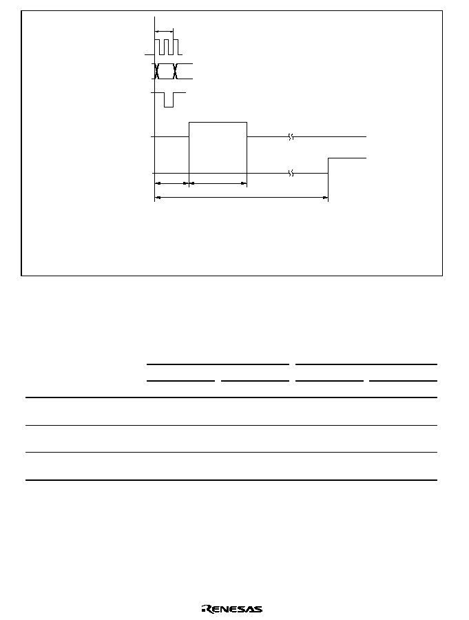
Rev. 2.0, 04/02, page 722 of 906
(1)
(2)
t
D
t
SPL
t
CONV
¯
Address
Write signal
Input sampling
timing
ADF
Legend
(1)
: ADCSR write cycle
(2)
: ADCSR address
t
D
: A/D conversion start delay time
t
SPL
: Input sampling time
t
CONV
: A/D conversion time
Figure 16.2 A/D Conversion Timing
Table 16.3
A/D Conversion Time (Single Mode)
∑
H8S/2678 Series
CKS1 = 0
CKS1 = 1
CKS = 0
CKS = 1
CKS = 0
CKS = 1
Item
Symbol
Min Typ Max
Min Typ Max
Min Typ Max
Min Typ Max
A/D conversion
start delay time
t
D
18
--
33
4
--
5
10
--
17
6
--
9
Input sampling
time
t
SPL
--
127 --
--
15
--
--
63
--
--
31
--
A/D conversion
time
t
CONV
515 --
530
67
--
68
259 --
266
131 --
134
Note: Values in the table are the number of states.

Rev. 2.0, 04/02, page 723 of 906
∑
H8S/2678R Series
CKS1 = 0
CKS1 = 1
CKS0 = 0
CKS0 = 1
CKS0 = 0
CKS0 = 1
Item
Symbol
Min Typ Max
Min Typ Max
Min Typ Max
Min Typ Max
A/D conversion
start delay time
t
D
18
--
33
10
--
17
6
--
9
4
--
5
Input sampling
time
t
SPL
--
127 --
--
63
--
--
31
--
--
15
--
A/D conversion
time
t
CONV
515 --
530
259 --
266
131 --
134
67
--
68
Note: Values in the table are the number of states.
Table 16.4
A/D Conversion Time (Scan Mode)
∑
H8S/2678 Series
CKS1
CKS
Conversion Time (State)
0
512 (Fixed)
0
1
64 (Fixed)
0
256 (Fixed)
1
1
128 (Fixed)
∑
H8S/2678R Series
CKS1
CKS0
Conversion Time (State)
0
512 (Fixed)
0
1
256 (Fixed)
0
128 (Fixed)
1
1
64 (Fixed)
16.4.4
External Trigger Input Timing
A/D conversion can be externally triggered. When the TRGS1 and TRGS0 bits are set to 11 in
ADCR, external trigger input is enabled at the
$'75* pin. A falling edge at the $'75* pin sets
the ADST bit to 1 in ADCSR, starting A/D conversion. Other operations, in both single and scan
modes, are the same as when the bit ADST has been set to 1 by software. Figure 16.3 shows the
timing.
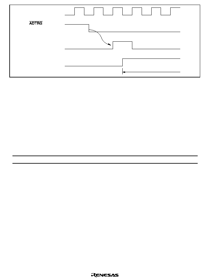
Rev. 2.0, 04/02, page 724 of 906
¯
Internal trigger signal
ADST
A/D conversion
Figure 16.3 External Trigger Input Timing
16.5
Interrupt Source
The A/D converter generates an A/D conversion end interrupt (ADI) at the end of A/D conversion.
Setting the ADIE bit to 1 enables an ADI interrupt requests while the bit ADF in ADCSR is set to
1 after A/D conversion is completed. The DTC or DMAC can be activated by an ADI interrupt.
Having the converted data read by the DTC or DMAC in response to an ADI interrupt enables
continuous conversion to be achieved without imposing a load on software.
Table 16.5
A/D Converter Interrupt Source
Name
Interrupt Source
Interrupt Flag
DTC Activation
DMAC Activation
ADI
End of conversion
ADF
Possible
Possible
16.6
A/D Conversion Accuracy Definitions
This LSI's A/D conversion accuracy definitions are given below.
∑
Resolution
The number of A/D converter digital output codes
∑
Quantization error
The deviation inherent in the A/D converter, given by 1/2 LSB (see figure 16.4).
∑
Offset error
The deviation of the analog input voltage value from the ideal A/D conversion characteristic
when the digital output changes from the minimum voltage value B'0000000000 (H'000) to
B'0000000001 (H'001) (see figure 16.5).
∑
Full-scale error
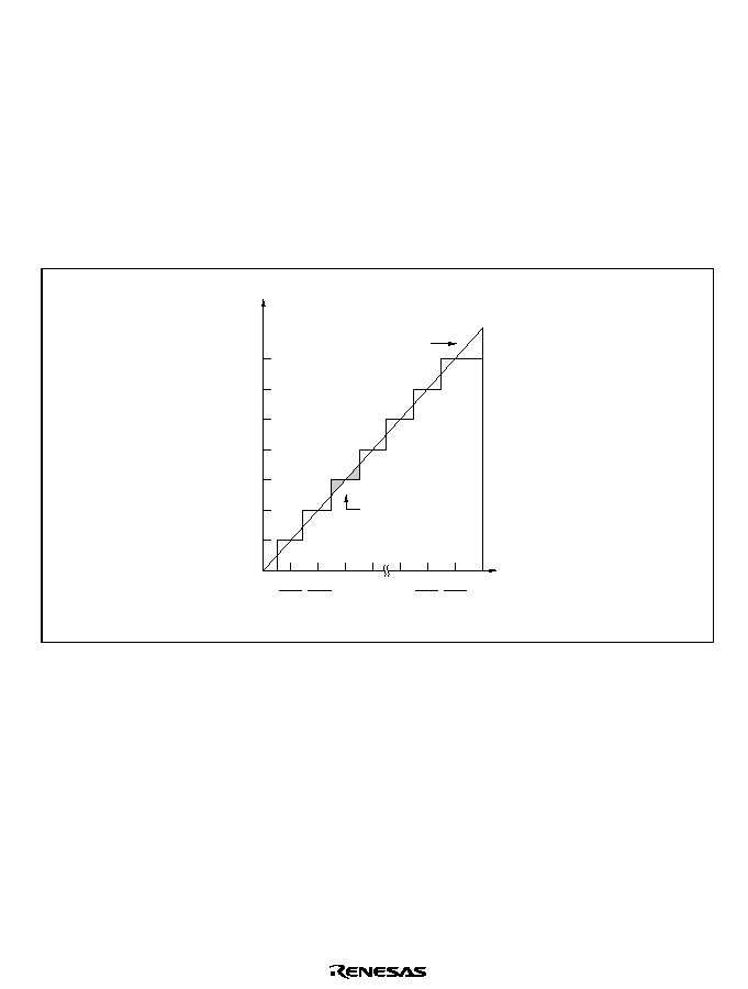
Rev. 2.0, 04/02, page 725 of 906
The deviation of the analog input voltage value from the ideal A/D conversion characteristic
when the digital output changes from B'1111111110 (H'3FE) to B'1111111111 (H'3FF) (see
figure 16.5).
∑
Nonlinearity error
The error with respect to the ideal A/D conversion characteristic between the zero voltage and
the full-scale voltage. Does not include the offset error, full-scale error, or quantization error
(see figure 16.5).
∑
Absolute precision
The deviation between the digital value and the analog input value. Includes the offset error,
full-scale error, quantization error, and nonlinearity error.
111
110
101
100
011
010
001
000
1
1024
2
1024
1022
1024
1023
1024
FS
Quantization error
Digital output
Ideal A/D conversion
characteristic
Analog
input voltage
Figure 16.4 A/D Conversion Accuracy Definitions
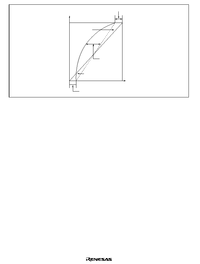
Rev. 2.0, 04/02, page 726 of 906
FS
Digital output
Ideal A/D conversion
characteristic
Nonlinearity
error
Analog
input voltage
Offset error
Actual A/D conversion
characteristic
Full-scale error
Figure 16.5 A/D Conversion Accuracy Definitions
16.7
Usage Notes
16.7.1
Module Stop Mode Setting
Operation of the A/D converter can be disabled or enabled using the module stop control register.
The initial setting is for operation of the A/D converter to be halted. Register access is enabled by
clearing module stop mode. For details, refer to section 22, Power-Down Modes.
16.7.2
Permissible Signal Source Impedance
This LSI's analog input is designed so that conversion precision is guaranteed for an input signal
for which the signal source impedance is 10 k
or less. This specification is provided to enable
the A/D converter's sample-and-hold circuit input capacitance to be charged within the sampling
time; if the sensor output impedance exceeds 10 k
, charging may be insufficient and it may not
be possible to guarantee the A/D conversion accuracy. However, if a large capacitance is
provided externally for conversion in single mode, the input load will essentially comprise only
the internal input resistance of 10 k
, and the signal source impedance is ignored. However, since
a low-pass filter effect is obtained in this case, it may not be possible to follow an analog signal
with a large differential coefficient (e.g., 5 mV/
µ
s or greater) (see figure 16.6). When converting a
high-speed analog signal or conversion in scan mode, a low-impedance buffer should be inserted.
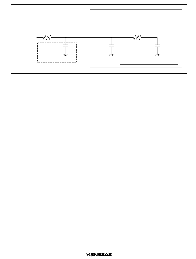
Rev. 2.0, 04/02, page 727 of 906
Equivalent circuit of A/D converter
This LSI
20 pF
Cin =
15 pF
10 k
Up to 10 k
Low-pass
filter
C to 0.1
µ
F
Sensor output
impedance
Sensor input
Figure 16.6 Example of Analog Input Circuit
16.7.3
Influences on Absolute Precision
Adding capacitance results in coupling with GND, and therefore noise in GND may adversely
affect absolute precision. Be sure to make the connection to an electrically stable GND such as
AVss.
Care is also required to insure that filter circuits do not communicate with digital signals on the
mounting board, so acting as antennas.
16.7.4
Setting Range of Analog Power Supply and Other Pins
If conditions shown below are not met, the reliability of the device may be adversely affected.
∑
Analog input voltage range
The voltage applied to analog input pin ANn during A/D conversion should be in the range
AVss
V
A
n
Vref.
∑
Relation between AVcc, AVss and Vcc, Vss
As the relationship between AVcc, AVss and Vcc, Vss, set AVcc
Vcc and AVss = Vss. If
the A/D converter is not used, the AVcc and AVss pins must not be left open.
∑
Vref setting range
The reference voltage at the Vref pin should be set in the range Vref
AVcc.

Rev. 2.0, 04/02, page 728 of 906
16.7.5
Notes on Board Design
In board design, digital circuitry and analog circuitry should be as mutually isolated as possible,
and layout in which digital circuit signal lines and analog circuit signal lines cross or are in close
proximity should be avoided as far as possible. Failure to do so may result in incorrect operation
of the analog circuitry due to inductance, adversely affecting A/D conversion values.
Also, digital circuitry must be isolated from the analog input signals (AN0 to AN7 and AN12 to
AN15), analog reference power supply (Vref), and analog power supply (AVcc) by the analog
ground (AVss). Also, the analog ground (AVss) should be connected at one point to a stable
digital ground (Vss) on the board.
16.7.6
Notes on Noise Countermeasures
A protection circuit connected to prevent damage due to an abnormal voltage such as an excessive
surge at the analog input pins (AN0 to AN7 and AN12 to AN15) should be connected between
AVcc and AVss as shown in figure 16.7. Also, the bypass capacitors connected to AVcc and the
filter capacitor connected to AN0 to AN7 and AN12 to AN15 must be connected to AVss.
If a filter capacitor is connected, the input currents at the analog input pins (AN0 to AN7 and
AN12 to AN15) are averaged, and so an error may arise. Also, when A/D conversion is
performed frequently, as in scan mode, if the current charged and discharged by the capacitance of
the sample-and-hold circuit in the A/D converter exceeds the current input via the input impedance
(R
in
), an error will arise in the analog input pin voltage. Careful consideration is therefore required
when deciding the circuit constants.
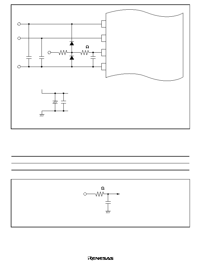
Rev. 2.0, 04/02, page 729 of 906
AV
CC
*
1
*
1
Vref
AN0 to AN7, AN12 to AN15
AV
SS
Notes:
Values are reference values.
1.
2. R
in
: Input impedance
R
in
*
2
100
0.1 µF
0.01 µF
10 µF
Figure 16.7 Example of Analog Input Protection Circuit
Table 16.6
Analog Pin Specifications
Item
Min
Max
Unit
Analog input capacitance
--
20
pF
Permissible signal source impedance
--
10
k
20 pF
To A/D
converter
AN0 to AN7,
AN12 to AN15
10 k
Note: Values are reference values.
Figure 16.8 Analog Input Pin Equivalent Circuit

Rev. 2.0, 04/02, page 730 of 906

Rev. 2.0, 04/02, page 731 of 906
Section 17 D/A Converter
17.1
Features
D/A converter features are listed below.
∑
8-bit resolution
∑
Four output channels
∑
Maximum conversion time of 10 µs (with 20 pF load)
∑
Output voltage of 0 V to Vref
∑
D/A output hold function in software standby mode
∑
Setting the module stop mode
DAC0001A_000020020400
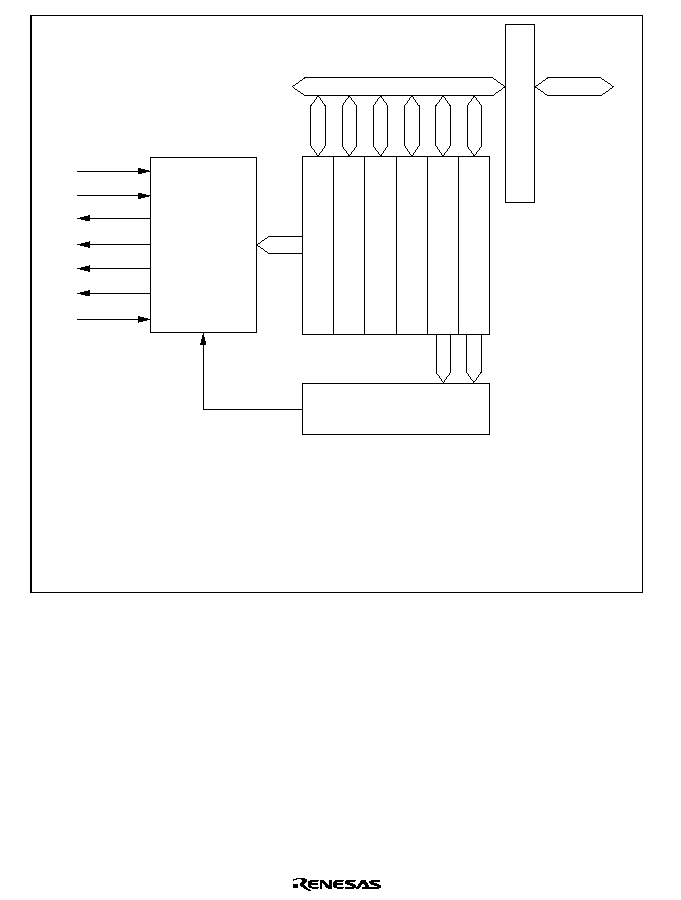
Rev. 2.0, 04/02, page 732 of 906
Module data bus
Internal data bus
Vref
AV
CC
DA3
DA2
DA1
DA0
AV
SS
8-bit
D/A
Control circuit
DADR0
DADR1
DADR2
DADR3
DACR01
DACR23
Bus interface
Legend
DADR0: D/A data register 0
DADR1: D/A data register 1
DADR2: D/A data register 2
DADR3: D/A data register 3
DACR01: D/A control register 01
DACR23: D/A control register 23
Figure 17.1 Block Diagram of D/A Converter
17.2
Input/Output Pins
Table 17.1 shows the pin configuration of the D/A converter.

Rev. 2.0, 04/02, page 733 of 906
Table 17.1
Pin Configuration
Pin Name
Symbol
I/O
Function
Analog power pin
AV
CC
Input
Analog power
Analog ground pin
AV
SS
Input
Analog ground
Reference voltage pin
Vref
Input
Reference voltage of D/A converter
Analog output pin 0
DA0
Output
Channel 0 analog output
Analog output pin 1
DA1
Output
Channel 1 analog output
Analog output pin 2
DA2
Output
Channel 2 analog output
Analog output pin 3
DA3
Output
Channel 3 analog output
17.3
Register Descriptions
The D/A converter has the following registers.
∑
D/A data register 0 (DADR0)
∑
D/A data register 1 (DADR1)
∑
D/A data register 2 (DADR2)
∑
D/A data register 3 (DADR3)
∑
D/A control register 01 (DACR01)
∑
D/A control register 23 (DACR23)
17.3.1
D/A Data Registers 0 to 3 (DADR0 to DADR3)
DADR0 to DADR3 are 8-bit readable/writable registers that store data for conversion.
Whenever output is enabled, the values in DADR are converted and output to the analog output
pins.
17.3.2
D/A Control Registers 01 and 23 (DACR01, DACR23)
DACR01 and DACR23 control the operation of the D/A converter.

Rev. 2.0, 04/02, page 734 of 906
DACR01
Bit
Bit Name
Initial Value
R/W
Description
7
DAOE1
0
R/W
D/A Output Enable 1
Controls D/A conversion and analog output.
0: Analog output (DA1) is disabled
1: Channel 1 D/A conversion is enabled; analog
output (DA1) is enabled
6
DAOE0
0
R/W
D/A Output Enable 0
Controls D/A conversion and analog output.
0: Analog output (DA0) is disabled
1: Channel 0 D/A conversion is enabled; analog
output (DA0) is enabled
5
DAE
0
R/W
D/A Enable
Used together with the DAOE0 and DAOE1 bits to
control D/A conversion. When the DAE bit is
cleared to 0, channel 0 and 1 D/A conversions are
controlled independently. When the DAE bit is set
to 1, channel 0 and 1 D/A conversions are
controlled together.
Output of conversion results is always controlled
independently by the DAOE0 and DAOE1 bits. For
details, see table 17.2 Control of D/A Conversion.
4
to
0
--
All 1
--
Reserved
These bits are always read as 1 and cannot be
modified.

Rev. 2.0, 04/02, page 735 of 906
Table 17.2
Control of D/A Conversion
Bit 5
DAE
Bit 7
DAOE1
Bit 6
DAOE0
Description
0
0
0
D/A conversion disabled
1
Channel 0 D/A conversion enabled, channel1 D/A conversion
disabled
1
0
Channel 1 D/A conversion enabled, channel0 D/A conversion
disabled
1
Channel 0 and 1 D/A conversions enabled
1
0
0
D/A conversion disabled
1
Channel 0 and 1 D/A conversions enabled
1
0
1

Rev. 2.0, 04/02, page 736 of 906
DACR23
Bit
Bit Name
Initial Value
R/W
Description
7
DAOE3
0
R/W
D/A Output Enable 3
Controls D/A conversion and analog output.
0: Analog output (DA3) is disabled
1: Channel 3 D/A conversion is enabled; analog
output (DA3) is enabled
6
DAOE2
0
R/W
D/A Output Enable 2
Controls D/A conversion and analog output.
0: Analog output (DA2) is disabled
1: Channel 2 D/A conversion is enabled; analog
output (DA2) is enabled
5
DAE
0
R/W
D/A Enable
Used together with the DAOE2 and DAOE3 bits to
control D/A conversion. When the DAE bit is
cleared to 0, channel 2 and 3 D/A conversions are
controlled independently. When the DAE bit is set
to 1, channel 2 and 3 D/A conversions are
controlled together.
Output of conversion results is always controlled
independently by the DAOE2 and DAOE3 bits. For
details, see table 17.3 Control of D/A Conversion.
4
to
0
--
All 1
--
Reserved
These bits are always read as 1 and cannot be
modified.

Rev. 2.0, 04/02, page 737 of 906
Table 17.3
Control of D/A Conversion
Bit 5
DAE
Bit 7
DAOE3
Bit 6
DAOE2
Description
0
0
0
D/A conversion disabled
1
Channel 2 D/A conversion enabled, channel3 D/A conversion
disabled
1
0
Channel 3 D/A conversion enabled, channel2 D/A conversion
disabled
1
Channel 2 and 3 D/A conversions enabled
1
0
0
D/A conversion disabled
1
Channel 2 and 3 D/A conversions enabled
1
0
1
17.4
Operation
The D/A converter includes D/A conversion circuits for four channels, each of which can operate
independently.
When DAOE bit in DACR01 or DACR23 is set to 1, D/A conversion is enabled and the
conversion result is output.
The operation example concerns D/A conversion on channel 0. Figure 17.2 shows the timing of
this operation.
[1] Write the conversion data to DADR0.
[2] Set the DAOE0 bit in DACR01 to 1. D/A conversion is started. The conversion result is output
from the analog output pin DA0 after the conversion time t
DCONV
has elapsed. The conversion
result is continued to output until DADR0 is written to again or the DAOE0 bit is cleared to 0.
The output value is expressed by the following formula:
[3] If DADR0 is written to again, the conversion is immediately started. The conversion result is
output after the conversion time t
DCONV
has elapsed.
[4] If the DAOE0 bit is cleared to 0, analog output is disabled.
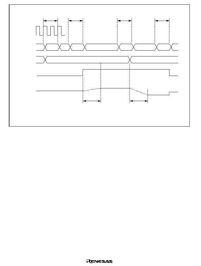
Rev. 2.0, 04/02, page 738 of 906
Conversion data 1
Conversion
result 1
High-impedance state
t
DCONV
DADR0
write cycle
DA0
DAOE0
DADR0
Address
¯
DACR01
write cycle
Conversion data 2
Conversion
result 2
t
DCONV
Legend
t
DCONV
: D/A conversion time
DADR0
write cycle
DACR01
write cycle
Figure 17.2 Example of D/A Converter Operation
17.5
Usage Notes
17.5.1
Setting for Module Stop Mode
It is possible to enable/disable the D/A converter operation using the module stop control register,
the D/A converter does not operate by the initial value of the register. The register can be accessed
by releasing the module stop mode. For details, see section 22, Power-Down Modes.
17.5.2
D/A Output Hold Function in Software Standby Mode
If D/A conversion is enabled and this LSI enters software standby mode, D/A output is held and
analog power supply current remains at the same level during D/A conversion. When the analog
power supply current is required to go low in software standby mode, bits DAOE0 to DAOE3 and
DAE should be cleared to 0, and D/A output should be disabled.

Rev. 2.0, 04/02, page 739 of 906
Section 18 RAM
This LSI has an on-chip high-speed static RAM. The RAM is connected to the CPU by a 16-bit
data bus, enabling one-state access by the CPU to both byte data and word data.
The on-chip RAM can be enabled or disabled by means of the RAME bit in the system control
register (SYSCR). For details on the system control register (SYSCR), refer to section 3.2.2,
System Control Register (SYSCR).
Product Type Name
ROM Type
RAM
Capacitance
RAM Address
HD64F2676
Flash memory version
8 kbytes
H
FFA000 to H
FFBFFF
HD6432676
Masked ROM version
8 kbytes
H
FFA000 to H
FFBFFF
HD6432675
8 kbytes
H
FFA000 to H
FFBFFF
HD6432673
8 kbytes
H
FFA000 to H
FFBFFF
H8S/2678
Series
HD6412670
ROMless version
8 kbytes
H
FFA000 to H
FFBFFF
H8S/2678R
Series
HD6412674R
ROMless version
32 kbytes
H
FF4000 to H
FFBFFF

Rev. 2.0, 04/02, page 740 of 906

Rev. 2.0, 04/02, page 741 of 906
Section 19 Flash Memory (F-ZTAT Version)
The features of the flash memory included in the flash memory version are summarized below.
The block diagram of the flash memory is shown in figure 19.1.
19.1
Features
∑
Size
Product Classification
ROM Size
ROM Address
H8S/2678 Series
HD64F2676
256 kbytes
H'000000 to H'03FFFF (Modes 3, 4, 7, 10, and 11)
H'100000 to H'13FFFF (Modes 5, 6, 13, and 14)
∑
Programming/erase methods
The flash memory is programmed 128 bytes at a time. Erase is performed in single-block
units. The flash memory of 384 kbytes is configured as follows: 64 kbytes
◊
5 blocks, 32
kbytes
◊
1 block, and 4 kbytes
◊
8 block. The 256-kbyte flash memory is configured as
follows: 64 kbytes
◊
3 blocks, 32 kbytes
◊
1 block, and 4 kbytes
◊
8 blocks. To erase the
entire flash memory, each block must be erased in turn.
∑
Reprogramming capability
The flash memory can be reprogrammed up to 100 times.
∑
Two on-board programming modes
Boot mode
User program mode
On-board programming/erasing can be done in boot mode in which the on-chip boot program
is started for erase or programming of the entire flash memory. In normal user program mode,
individual blocks can be erased or programmed.
∑
Programmer mode
Flash memory can be programmed/erased in programmer mode, using a PROM programmer,
as well as in on-board programming mode.
∑
Automatic bit rate adjustment
With data transfer in boot mode, the bit rate of this LSI can be automatically adjusted to match
the transfer bit rate of the host.
∑
Flash memory emulation by RAM
Part of the RAM area can be overlapped onto flash memory, to emulate flash memory updates
in real time.
∑
Programming/erasing protection
There are three protect modes, hardware, software, and error protect, which allow protected
status to be designated for flash memory program/erase operations.
ROMF251A_000020020400
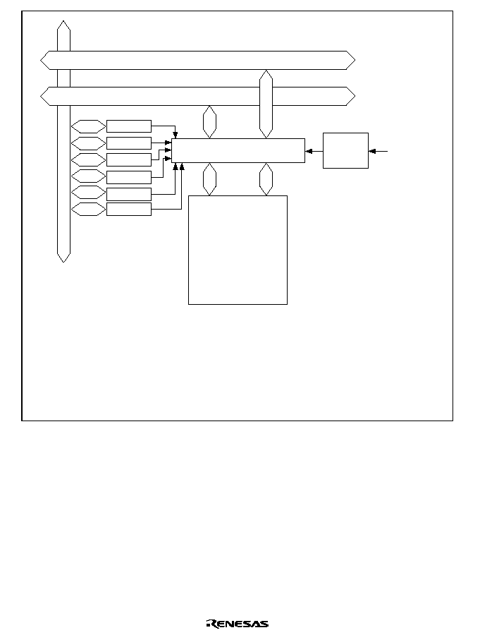
Rev. 2.0, 04/02, page 742 of 906
Module bus
Bus interface/controller
Flash memory
Operating
mode
EBR1
Internal address bus
Internal data bus (16 bits)
FWE pin
*
Mode pins
EBR2
SYSCR
FLMCR2
FLMCR1
RAMER
Legend
FLMCR1: Flash memory control register 1
FLMCR2: Flash memory control register 2
EBR1:
Erase block register 1
EBR2:
Erase block register 2
RAMER:
RAM emulation register
SYSCR:
System control register
Note:
*
Only in H8S/2678 series.
Figure 19.1 Block Diagram of Flash Memory
19.2
Mode Transitions
When the mode pins and the FWE pin* are set in the reset state and a reset-start is executed, this
LSI enters an operating mode as shown in figure 19.2. In user mode, flash memory can be read but
not programmed or erased.
The boot, user program and programmer modes are provided as modes to write and erase the flash
memory.
The differences between boot mode and user program mode are shown in table 19.1. Figure 19.3
shows boot mode. Figure 19.4 shows user program mode.
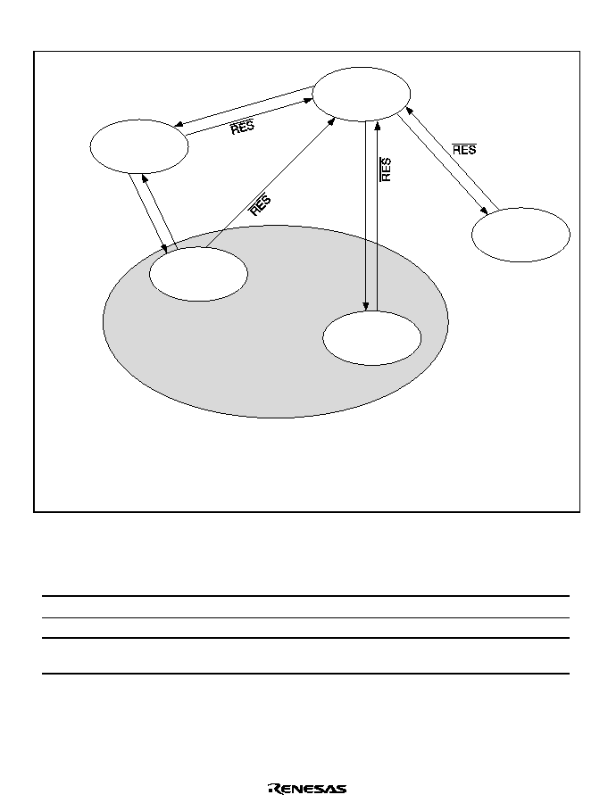
Rev. 2.0, 04/02, page 743 of 906
Note:
Only in the H8S/2678 Series.
Boot mode
On-board programming mode
User
program mode
User mode
(on-chip ROM
enabled)
Reset state
Programmer
mode
= 0
FWE = 1, MD2 = 1,
SWE = 1
*
1
SWE = 1
*
2
FWE = 0, MD2 = 1,
SWE = 0
*
1
SWE = 0
*
2
Notes: Only make a transition between user mode and user program mode when the CPU is
not accessing the flash memory.
*
1 Only in H8S/2678 series.
*
2 Only in H8S/2678R series.
= 0
= 0
= 0
MD2 = 1,
FWE = 0
*
1
MD2 = 1
*
2
MD1 = 1, MD2 = 0, FWE = 1
*
1
MD0 = 1, MD1 = 1, MD2 = 0
*
2
MD0 = 0, MD1 = 0,
MD2 = 0, P50 = 0,
P51 = 0, P52 = 1
Figure 19.2 Flash Memory State Transitions
Table 19.1
Differences between Boot Mode and User Program Mode
Boot Mode
User Program Mode
Total erase
Yes
Yes
Block erase
No
Yes
Programming control program
*
Program/program-verify Erase/erase-verify/program/
program-verify emulation
Note: To be provided by the user, in accordance with the recommended algorithm.
Rev. 2.0, 04/02, page 744 of 906
Flash memory
This LSI
RAM
Host
Programming control
program
SCI
Application program
(old version)
�
U
Z
`
New application
program
Flash memory
This LSI
RAM
Host
SCI
Application program
(old version)
Boot program area
New application
program
Flash memory
This LSI
RAM
Host
SCI
Flash memory
prewrite-erase
Boot program
New application
program
Flash memory
This LSI
Program execution state
RAM
Host
SCI
New application
program
Boot program
Programming control
program
"
|
~
S
`a
,
y
P
P
Q
R
V
W
!
"
|
^
_
c
1. Initial state
The old program version or data remains written
in the flash memory. The user should prepare the
programming control program and new
application program beforehand in the host.
2. Programming control program transfer
When boot mode is entered, the boot program in
the chip (originally incorporated in the chip) is
started and the programming control program in
the host is transferred to RAM via SCI
communication. The boot program required for
flash memory erasing is automatically transferred
to the RAM boot program area.
3. Flash memory initialization
The erase program in the boot program area (in
RAM) is executed, and the flash memory is
initialized (to H'FF). In boot mode, entire flash
memory erasure is performed, without regard to
blocks.
4. Writing new application program
The programming control program transferred
from the host to RAM is executed, and the new
application program in the host is written into the
flash memory.
Programming control
program
Boot program
Boot program
Boot program area
Boot program area
Programming control
program
Figure 19.3 Boot Mode
Rev. 2.0, 04/02, page 745 of 906
Flash memory
This LSI
RAM
Host
Programming/
erase control program
SCI
Boot program
New application
program
Flash memory
This LSI
RAM
Host
SCI
New application
program
Flash memory
This LSI
RAM
Host
SCI
Flash memory
erase
Boot program
New application
program
Flash memory
This LSI
Program execution state
RAM
Host
SCI
Boot program
!
,
Boot program
FWE assessment
program
Application program
(old version)
,
New application
program
1. Initial state
(1) The FWE assessment program that confirms
that user program mode is entered, and (2) the
program that will transfer the programming/ erase
control program to on-chip RAM should be
written into the flash memory by the user
beforehand. (3) The programming/erase control
program should be prepared in the host or in the
flash memory.
2. Programming/erase control program transfer
When user program mode is entered, user
software confirms this fact, executes the transfer
program in the flash memory, and transfers the
programming/erase control program to RAM.
3. Flash memory initialization
The programming/erase program in RAM is
executed, and the flash memory is initialized (to
H'FF). Erasing can be performed in block units,
but not in byte units.
4. Writing new application program
Next, the new application program in the host is
written into the erased flash memory blocks. Do
not write to unerased blocks.
Programming/
erase control program
Programming/
erase control program
Programming/
erase control program
Transfer program
Application program
(old version)
Transfer program
FWE assessment
program
FWE assessment
program
Transfer program
FWE assessment
program
Transfer program
Note: The FWE assessment program is not available in the H8S/2678R series.
Figure 19.4 User Program Mode

Rev. 2.0, 04/02, page 746 of 906
19.3
Block Configuration
Figure 19.5 shows the block configuration of 384-kbyte flash memory and figure 19.6 shows that
of 256-kbyte flash memory. The thick lines indicate erasing units, the narrow lines indicate
programming units, and the values are addresses. The 384-kbyte flash memory is divided into 64
kbytes (5 blocks), 32 kbytes (1 block), and 4 kbytes (8 blocks). The 256-kbyte flash memory is
divided into 64 kbytes (3 blocks), 32 kbytes (1 block), and 4 kbytes (8 blocks). Erasing is
performed in these divided units. Programming is performed in 128-byte units starting from an
address whose lower eight bits are H'00 or H'80.
Rev. 2.0, 04/02, page 747 of 906
EB0
Erase unit
4 kbytes
EB1
Erase unit
4 kbytes
EB2
Erase unit
4 kbytes
EB3
Erase unit
4 kbytes
EB4
Erase unit
4 kbytes
EB7
Erase unit
4 kbytes
EB8
Erase unit
32 kbytes
EB9
Erase unit
64 kbytes
EB10
Erase unit
64 kbytes
EB11
Erase unit
64 kbytes
H'000000
H'000001
H'000002
H'00007F
H'000FFF
H'00107F
H'00207F
H'00307F
H'00407F
H'00707F
H'007FFF
H'001FFF
H'002FFF
H'003FFF
H'03FFFF
H'00807F
H'00FFFF
H'01007F
H'01FFFF
H'02007F
H'02FFFF
H'03007F
H'001000
H'001001
H'001002
H'002000
H'002001
H'002002
H'003000
H'003001
H'003002
H'004000
H'004001
H'004002
H'007000
H'007001
H'007002
H'008000
H'008001
H'008002
H'010000
H'010001
H'010002
H'020000
H'020001
H'020002
H'030000
H'030001
H'030002
Programming unit: 128 bytes
Programming unit: 128 bytes
EB12
Erase unit
64 kbytes
EB13
Erase unit
64 kbytes
H'05FFFF
H'04007F
H'04FFFF
H'05007F
H'040000
H'040001
H'040002
H'050000
H'050001
H'050002
Programming unit: 128 bytes
Programming unit: 128 bytes
Programming unit: 128 bytes
Programming unit: 128 bytes
Programming unit: 128 bytes
Programming unit: 128 bytes
Programming unit: 128 bytes
Programming unit: 128 bytes
Programming unit: 128 bytes
Programming unit: 128 bytes
Note: Addresses H'100000 to H'15FFFF are allocated in modes 5 and 6.
Figure 19.5 384-Kbyte Flash Memory Block Configuration (Modes 3, 4, and 7)
Rev. 2.0, 04/02, page 748 of 906
EB0
Erase unit
4 kbytes
EB1
Erase unit
4 kbytes
EB2
Erase unit
4 kbytes
EB3
Erase unit
4 kbytes
EB4
Erase unit
4 kbytes
EB7
Erase unit
4 kbytes
EB8
Erase unit
32 kbytes
EB9
Erase unit
64 kbytes
EB10
Erase unit
64 kbytes
EB11
Erase unit
64 kbytes
H'000000
H'000001
H'000002
H'00007F
H'000FFF
H'00107F
H'00207F
H'00307F
H'00407F
H'00707F
H'007FFF
H'001FFF
H'002FFF
H'003FFF
H'03FFFF
H'00807F
H'00FFFF
H'01007F
H'01FFFF
H'02007F
H'02FFFF
H'03007F
H'001000
H'001001
H'001002
H'002000
H'002001
H'002002
H'003000
H'003001
H'003002
H'004000
H'004001
H'004002
H'007000
H'007001
H'007002
H'008000
H'008001
H'008002
H'010000
H'010001
H'010002
H'020000
H'020001
H'020002
H'030000
H'030001
H'030002
Programming unit: 128 bytes
Programming unit: 128 bytes
Programming unit: 128 bytes
Programming unit: 128 bytes
Programming unit: 128 bytes
Programming unit: 128 bytes
Programming unit: 128 bytes
Programming unit: 128 bytes
Programming unit: 128 bytes
Programming unit: 128 bytes
Note: Addresses H'100000 to H'13FFFF are allocated in modes 5, 6, 13, and 14.
Figure 19.6 256-Kbyte Flash Memory Block Configuration (Modes 4, 7, 10, and 11)

Rev. 2.0, 04/02, page 749 of 906
19.4
Input/Output Pins
Table 19.2 shows the pin configuration of the flash memory.
Table 19.2
Pin Configuration
Pin Name
I/O
Function
#$
Input
Reset
FWE
*
Input
Flash program/erase protection by hardware
MD2
Input
Sets this LSI's operating mode
MD1
Input
Sets this LSI's operating mode
MD0
Input
Sets this LSI's operating mode
P52
Input
Sets operating mode in programmer mode
P51
Input
Sets operating mode in programmer mode
P50
Input
Sets operating mode in programmer mode
TxD1
Output
Serial transmit data output
RxD1
Input
Serial receive data input
Note: Only in H8S/2678 Series.
19.5
Register Descriptions
The flash memory has the following registers. For details on the system control register, refer to
section 3.2.2, System Control Register (SYSCR).
∑
Flash memory control register 1 (FLMCR1)
∑
Flash memory control register 2 (FLMCR2)
∑
Erase block register 1 (EBR1)
∑
Erase block register 2 (EBR2)
∑
RAM emulation register (RAMER)
19.5.1
Flash Memory Control Register 1 (FLMCR1)
FLMCR1 is a register that makes the flash memory transit to program mode, program-verify
mode, erase mode, or erase-verify mode. For details on register setting, refer to section 19.8,
Flash Memory Programming/Erasing.

Rev. 2.0, 04/02, page 750 of 906
Bit
Bit Name
Initial Value
R/W
Description
7
FWE
0/1
R
Flash Write Enable
Reflects the input level at the FWE pin. It is set to 1
when a high level is input to the FWE pin, and
cleared to 0 when a low level is input. When this bit
is cleared to 0, the flash memory transits to the
hardware protection state.
Note: In the H8S/2678R Series, this bit is
reserved. This bit is always read as 0 in
modes 1 and 2. This bit is always read as 1
in modes 3 to 7. The initial value should not
be changed.
6
SWE
0
R/W
Software Write Enable
When this bit is set to 1, flash memory
programming/erasing is enabled. When this bit is
cleared to 0, other FLMCR1 register bits and all
EBR1 and EBR2 bits cannot be set.
5
ESU
0
R/W
Erase Setup
When this bit is set to 1
while
FWE
= 1
*
and SWE
= 1, the flash memory transits to the erase setup
state. When it is cleared to 0, the erase setup state
is cancelled.
4
PSU
0
R/W
Program Setup
When this bit is set to 1 while
FWE
= 1
*
and SWE
= 1, the flash memory transits to the program setup
state. When it is cleared to 0, the program setup
state is cancelled.
3
EV
0
R/W
Erase-Verify
When this bit is set to 1 while
FWE
= 1
*
and SWE
= 1, the flash memory transits to erase-verify
mode. When it is cleared to 0, erase-verify mode is
cancelled.
2
PV
0
R/W
Program-Verify
When this bit is set to 1 while
FWE
= 1
*
and SWE
= 1, the flash memory transits to program-verify
mode. When it is cleared to 0, program-verify
mode is cancelled.
1
E
0
R/W
Erase
When this bit is set to 1 while FWE
= 1
*
, SWE = 1,
and ESU = 1, the flash memory transits to erase
mode. When it is cleared to 0, erase mode is
cancelled.

Rev. 2.0, 04/02, page 751 of 906
Bit
Bit Name
Initial Value
R/W
Description
0
P
0
R/W
Program
When this bit is set to 1 while FWE
= 1
*
, SWE = 1,
and PSU = 1, the flash memory transits to program
mode. When it is cleared to 0, program mode is
cancelled.
Note: Only in H8S/2678 Series.
19.5.2
Flash Memory Control Register 2 (FLMCR2)
FLMCR2 is a register that displays the state of flash memory programming/erasing. FLMCR2 is a
read-only register, and should not be written to. When the on-chip flash memory is disabled, the
contents of FLMCR2 are always read as H'00.
Bit
Bit Name
Initial Value
R/W
Description
7
FLER
0
R
Indicates that an error has occurred during an
operation on flash memory (programming or
erasing). When FLER is set to 1, flash memory
goes to the error-protection state.
See 19.9.3 Error Protection, for details.
6
to
0
--
All 0
R
Reserved
These bits always read as 0.
19.5.3
Erase Block Register 1 (EBR1)
EBR1 specifies the flash memory erase area block. EBR1 is initialized to H'00 when the SWE bit
in FLMCR1 is 0. Set only one bit in EBR1 and EBR2 together (do not set more than one bit at the
same time). Setting more than one bit will automatically clear all EBR1 and EBR2 bits to 0. For
details, see table 19.3, Erase Blocks.

Rev. 2.0, 04/02, page 752 of 906
Bit
Bit Name
Initial Value
R/W
Description
7
EB7
0
R/W
When this bit is set to 1, 4 kbytes of EB7 are to be
erased.
6
EB6
0
R/W
When this bit is set to 1, 4 kbytes of EB6 are to be
erased.
5
EB5
0
R/W
When this bit is set to 1, 4 kbytes of EB5 are to be
erased.
4
EB4
0
R/W
When this bit is set to 1, 4 kbytes of EB4 are to be
erased.
3
EB3
0
R/W
When this bit is set to 1, 4 kbytes of EB3 is to be
erased.
2
EB2
0
R/W
When this bit is set to 1, 4 kbytes of EB2 is to be
erased.
1
EB1
0
R/W
When this bit is set to 1, 4 kbytes of EB1 is to be
erased.
0
EB0
0
R/W
When this bit is set to 1, 4 kbytes of EB0 is to be
erased.
19.5.4
Erase Block Register 2 (EBR2)
EBR2 specifies the flash memory erase area block. EBR2 is initialized to H'00 when the SWE bit
in FLMCR1 is 0. Set only one bit in EBR2 and EBR1 together (do not set more than one bit at the
same time). Setting more than one bit will automatically clear all EBR1 and EBR2 bits to 0. For
details, see table 19.3, Erase Blocks.

Rev. 2.0, 04/02, page 753 of 906
Bit
Bit Name
Initial Value
R/W
Description
7, 6
--
0
R/W
Reserved
The initial value should not be changed.
5
EB13
0
R/W
When this bit is set to 1, 64 kbytes of EB13 are to
be erased.
Note: In the H8S/2678 Series, this bit is reserved.
The initial value should not be changed.
4
EB12
0
R/W
When this bit is set to 1, 64 kbytes of EB12 are to
be erased.
Note: In the H8S/2678 Series, this bit is reserved.
The initial value should not be changed.
3
EB11
0
R/W
When this bit is set to 1, 64 kbytes of EB11 are to
be erased.
2
EB10
0
R/W
When this bit is set to 1, 64 kbytes of EB10 are to
be erased.
1
EB9
0
R/W
When this bit is set to 1, 64 kbytes of EB9 are to be
erased.
0
EB8
0
R/W
When this bit is set to 1, 32 kbytes of EB8 are to be
erased.

Rev. 2.0, 04/02, page 754 of 906
Table 19.3
Erase Blocks
Address
Block (Size)
H8S/2678R Series: Modes 3, 4, and 7
H8S/2678 Series: Modes 4, 7, 10, and 11
H8S/2678R Series: Modes 5 and 6
H8S/2678 Series: Modes 5, 6, 13, and 14
EB0 (4 kbytes)
H'000000 to H'000FFF
H'100000 to H'100FFF
EB1 (4 kbytes)
H'001000 to H'001FFF
H'101000 to H'101FFF
EB2 (4 kbytes)
H'002000 to H'002FFF
H'102000 to H'102FFF
EB3 (4 kbytes)
H'003000 to H'003FFF
H'103000 to H'103FFF
EB4 (4 kbytes)
H'004000 to H'004FFF
H'104000 to H'104FFF
EB5 (4 kbytes)
H'005000 to H'005FFF
H'105000 to H'105FFF
EB6 (4 kbytes)
H'006000 to H'006FFF
H'106000 to H'106FFF
EB7 (4 kbytes)
H'007000 to H'007FFF
H'107000 to H'107FFF
EB8 (32 kbytes)
H'008000 to H'00FFFF
H'108000 to H'10FFFF
EB9 (64 kbytes)
H'010000 to H'01FFFF
H'110000 to H'11FFFF
EB10 (64 kbytes) H'020000 to H'02FFFF
H'120000 to H'12FFFF
EB11 (64 kbytes) H'030000 to H'03FFFF
H'130000 to H'13FFFF
EB12 (64 kbytes) H'040000 to H'04FFFF
H'140000 to H'14FFFF
EB13 (64 kbytes) H'050000 to H'05FFFF
H'150000 to H'15FFFF
Note: The erase blocks of the 384-kbyte flash memory are EB0 to EB13.
The erase blocks of the 256-kbyte flash memory are EB0 to EB11.
19.5.5
RAM Emulation Register (RAMER)
RAMER specifies the area of flash memory to be overlapped with part of RAM when emulating
real-time flash memory programming. RAMER settings should be made in user mode or user
program mode. To ensure correct operation of the emulation function, the ROM for which RAM
emulation is performed should not be accessed immediately after this register has been modified.
Normal execution of an access immediately after register modification is not guaranteed.

Rev. 2.0, 04/02, page 755 of 906
Bit
Bit Name
Initial Value
R/W
Description
7
and
5
--
All 0
R
Reserved
These bits always read as 0.
4
--
0
R/W
Reserved
The initial value should not be changed.
3
RAMS
0
R/W
RAM Select
Specifies selection or non-selection of flash
memory emulation in RAM. When RAMS = 1, the
flash memory is overlapped with part of RAM, and
all flash memory block are in the program/erase-
protect state. When this bit is cleared to 0, the RAM
emulation function is invalid.
2
1
0
RAM2
RAM1
RAM0
0
0
0
R/W
R/W
R/W
Flash Memory Area Selection
When the RAMS bit is set to 1, selects one of the
following flash memory areas to overlap the RAM
area. The areas correspond with 4-kbyte erase
blocks.
H8S/2678R Series: Modes 3, 4, and 7
H8S/2678 Series: Modes 4, 7, 10, and 11
000: H'000000 to H'000FFF (EB0)
001: H'001000 to H'001FFF (EB1)
010: H'002000 to H'002FFF (EB2)
011: H'003000 to H'003FFF (EB3)
100: H'004000 to H'004FFF (EB4)
101: H'005000 to H'005FFF (EB5)
110: H'006000 to H'006FFF (EB6)
111: H'007000 to H'007FFF (EB7)
H8S/2678R Series: Modes 5 and 6
H8S/2678 Series: Modes 5, 6, 13, and 14
000: H'100000 to H'100FFF (EB0)
001: H'101000 to H'101FFF (EB1)
010: H'102000 to H'102FFF (EB2)
011: H'103000 to H'103FFF (EB3)
100: H'104000 to H'104FFF (EB4)
101: H'105000 to H'105FFF (EB5)
110: H'106000 to H'106FFF (EB6)
111: H'107000 to H'107FFF (EB7)

Rev. 2.0, 04/02, page 756 of 906
19.6
On-Board Programming Modes
In an on-board programming mode, programming, erasing, and verification for the on-chip flash
memory can be performed. There are two on-board programming modes: boot mode and user
program mode. Table 19.4 shows how to select boot mode. User program mode can be selected by
setting the control bits by software. For a diagram that shows mode transitions of flash memory,
see figure 19.2.
Table 19.4
Setting On-Board Programming Modes
∑
H8S/2678 Series
Mode Setting
FWE
MD2
MD1
MD0
Boot mode
Expanded mode with on-chip
ROM enabled
1
0
1
0
Single-chip activation expanded
mode with on-chip ROM enabled
1
0
1
1
User program mode
Expanded mode with on-chip
ROM enabled
1
1
0
0
External ROM activation expanded
mode with on-chip ROM enabled
*
1
1
1
0
1
External ROM activation expanded
mode with on-chip ROM enabled
*
2
1
1
1
0
Single-chip activation expanded
mode with on-chip ROM enabled
1
1
1
1
Notes: 1. The initial setting for the external bus width is 16 bits.
2. The initial setting for the external bus width is 8 bits
∑
H8S/2678R Series
Mode Setting
MD2
MD1
MD0
Boot mode
Single-chip activation expanded
mode with on-chip ROM enabled
0
1
1
19.6.1
Boot Mode
When this LSI enters boot mode, the embedded boot program is started. The boot program
transfers the programming control program from the externally connected host to the on-chip
RAM via the SCI_1. When the flash memory is all erased, the programming control program is
executed.
Table 19.5 shows the boot mode operations between reset end and branching to the programming
control program.

Rev. 2.0, 04/02, page 757 of 906
1. When the boot program is initiated, the SCI_1 should be set to asynchronous mode, the chip
measures the low-level period of asynchronous SCI communication data (H'00) transmitted
continuously from the host. The chip then calculates the bit rate of transmission from the host,
and adjusts the SCI_1 bit rate to match that of the host. The transfer format is 8-bit data, 1 stop
bit, and no parity. The reset should end with the RxD pin high. The RxD and TxD pins should
be pulled up on the board if necessary. After the reset ends, it takes approximately 100 states
before the chip is ready to measure the low-level period.
2. After matching the bit rates, the chip transmits one H'00 byte to the host to indicate the end of
bit rate adjustment. The host should confirm that this adjustment end indication (H'00) has
been received normally, and transmit one H'55 byte to the chip. If reception could not be
performed normally, initiate boot mode again by a reset. Depending on the host's transfer bit
rate and system clock frequency of this LSI, there will be a discrepancy between the bit rates
of the host and the chip. To operate the SCI properly, set the host's transfer bit rate and system
clock frequency of this LSI within the ranges listed in table 19.6.
3. When boot mode is used, the flash memory programming control program must be prepared in
the host beforehand. Prepare a programming control program in accordance with the
description in section 19.8, Flash Memory Programming/Erasing.
4. Before branching to the programming control program, the chip terminates transfer operations
by the SCI_1 (by clearing the RE and TE bits in SCR to 0), but the adjusted bit rate value
remains set in BRR. Therefore, the programming control program can still use it for transfer
of program data or verify data with the host. The TxD pin is high. The contents of the CPU
general registers are undefined immediately after branching to the programming control
program. These registers must be initialized at the beginning of the programming control
program, since the stack pointer (SP), in particular, is used implicitly in subroutine calls, etc.
5. In boot mode, if flash memory contains data (all data is not 1), all blocks of flash memory are
erased. Boot mode is used for the initial programming in the on-board state or for a forcible
return when a program that is to be initiated in user program mode was accidentally erased and
could not be executed in user program mode.
Notes: 1. In boot mode, a part of the on-chip RAM area (H'FF8000 to H'FF87FF) is used by the
boot program. Addresses H'FF8800 to H'FFBFFF is the area to which the
programming control program is transferred from the host. The boot program area
cannot be used until the execution state in boot mode switches to the programming
control program.
2. Boot mode can be cleared by a reset. Release the reset by setting the MD pins, after
waiting at least 20 states since driving the reset pin low. Boot mode is also cleared
when the WDT overflow reset occurs.
3. Do not change the MD pin input levels in boot mode.
4.
All interrupts are disabled during programming or erasing of the flash memory.
Rev. 2.0, 04/02, page 758 of 906
Table 19.5
Boot Mode Operation
Communication Contents
Processing Contents
Host Operation
LSI Operation
Processing Contents
Continuously transmits data H'00
at specified bit rate.
Branches to boot program at reset-start.
Boot program initiation
H'00, H'00 . . . H'00
H'00
H'55
Transmits data H'55 when data H'00
is received error-free.
H'AA reception
H'XX
Transmits number of bytes (N) of
programming control program to be
transferred as 2-byte data
(low-order byte following high-order
byte)
Transmits 1-byte of programming
control program (repeated for N times)
H'AA reception.
Upper bytes, lower bytes
Echoback
Echoback
H'AA
Branches to programming control program
transferred to on-chip RAM and starts
execution.
Checks flash memory data, erases all flash
memory blocks in case of written data
existing, and transmits data H'AA to host.
(If erase could not be done, transmits data
H'FF to host and aborts operation.)
H'FF
Boot program
erase error
H'AA
Item
Boot mode initiation
∑ Measures low-level period of receive data H'00.
∑ Calculates bit rate and sets BRR in SCI_1.
∑ Transmits data H'00 to host as adjustment end
indication.
Transmits data H'AA to host when data H'55 is
received.
Bit rate adjustment
Echobacks the 2-byte data
received to host.
Echobacks received data to host and also
transfers it to RAM.
(repeated for N times)
Transfer of number of bytes of
programming control program
Flash memory erase
Table 19.6
System Clock Frequencies for which Automatic Adjustment of LSI Bit Rate is
Possible
Host Bit Rate
System Clock Frequency Range of LSI
19,200 bps
8 to 25 MHz
9,600 bps
8 to 25 MHz
Rev. 2.0, 04/02, page 759 of 906
19.6.2
User Program Mode
On-board programming/erasing of an individual flash memory block can also be performed in user
program mode by branching to a user program/erase program. The user must set branching
conditions and provide on-board means of supplying programming data. The flash memory must
contain the program/erase program or a program which provides the program/erase program from
external memory. Because the flash memory itself cannot be read during programming/erasing,
transfer the program/erase program to on-chip RAM, as like in boot mode. Figure 19.7 shows a
sample procedure for programming/erasing in user program mode. Prepare a program/erase
program in accordance with the description in section 19.8, Flash Memory Programming/Erasing.
Yes
No
Program/erase?
Transfer user program/erase control
program to RAM
Reset-start
Branch to user program/erase control
program in RAM
Execute user program/erase control
program (flash memory programming)
Branch to flash memory application
program
Branch to flash memory application
program
FWE=high
*
Clear FWE*
Not available in H8S/2678R series.
Note:
*
Figure 19.7 Programming/Erasing Flowchart Example in User Program Mode
Rev. 2.0, 04/02, page 760 of 906
19.7
Flash Memory Emulation in RAM
Making a setting in the RAM emulation register (RAMER) enables RAM to be overlapped onto
the part of flash memory area so that data to be programmed to flash memory can be emulated in
the on-chip RAM in real time. Emulation can be performed in user mode or user program mode.
Figure 19.8 shows an example of emulation of real-time flash memory programming.
1. Set RAMER to overlap RAM onto the area for which real-time programming is required.
2. Emulation is performed using the overlapping RAM.
3. After the program data has been confirmed, the RAMS bit is cleared, thus releasing RAM
overlap.
4. The data written in the overlapping RAM is written into the flash memory space (EB0).
Start of emulation program
Set RAMER
Write tuning data to overlap
RAM
Execute application program
Tuning OK?
Clear RAMER
Write to flash memory
emulation block
End of emulation program
No
Yes
Figure 19.8 Flowchart for Flash Memory Emulation in RAM
Example in which flash memory block is overlapped is shown in figure 19.9.
1. The RAM area to be overlapped is fixed at a 4-kbyte area in the range of H'FFA000 to
H'FFAFFF.
2. The flash memory area to overlap is selected by RAMER from a 4-kbyte area among one of
the EB0 to EB7 blocks.
Rev. 2.0, 04/02, page 761 of 906
3. The overlapped RAM area can be accessed from both the flash memory addresses and RAM
addresses.
Notes: 1. When the RAMS bit in RAMER is set to 1, program/erase protection is enabled for all
flash memory blocks (emulation protection). In this state, setting the P or E bit in
FLMCR1 to 1 does not cause a transition to program mode or erase mode.
2. A RAM area cannot be erased by execution of software in accordance with the erase
algorithm.
3. Block area EB0 contains the vector table. When performing RAM emulation, the
vector table is needed in the overlap RAM.
H'00000
H'01000
H'02000
H'03000
H'04000
H'05000
H'06000
H'07000
H'08000
H'5FFFF
Flash memory
EB8 to EB13
This area can be accessed
from both the RAM area
and flash memory area
EB0
EB1
EB2
EB3
EB4
EB5
EB6
EB7
H'FFA000
H'FFAFFF
H'FFBFFF
On-chip RAM
384-kbyte flash memory
Figure 19.9 Example of RAM Overlap Operation

Rev. 2.0, 04/02, page 762 of 906
19.8
Flash Memory Programming/Erasing
A software method, using the CPU, is employed to program and erase flash memory in the on-
board programming modes. Depending on the FLMCR1 and FLMCR2 setting, the flash memory
operates in one of the following four modes: program mode, erase mode, program-verify mode,
and erase-verify mode. The programming control program in boot mode and the user
program/erase program in user mode use these operating modes in combination to perform
programming/erasing. Flash memory programming and erasing should be performed in
accordance with the descriptions in section 19.8.1, Program/Program-Verify and section 19.8.2,
Erase/Erase-Verify, respectively.
19.8.1
Program/Program-Verify
When programming data or programs to the flash memory, the program/program-verify flowchart
shown in figure 19.10 should be followed. Performing programming operations according to this
flowchart will enable data or programs to be programmed to the flash memory without subjecting
the chip to voltage stress or sacrificing program data reliability.
1. Programming must be done to an empty address. Do not reprogram an address to which
programming has already been performed.
2. Programming should be carried out 128 bytes at a time. A 128-byte data transfer must be
performed even if programming fewer than 128 bytes. In this case, H'FF data must be written
to the extra addresses.
3. Prepare the following data storage areas in RAM: a 128-byte programming data area, a 128-
byte reprogramming data area, and a 128-byte additional-programming data area. Perform
reprogramming data computation and additional programming data computation according to
figure 19.10.
4. Consecutively transfer 128 bytes of data in byte units from the programming data area,
reprogramming data area, or additional-programming data area to the flash memory. The
program address and 128-byte data are latched in the flash memory. The lower 8 bits of the
start address in the flash memory destination area must be H'00 or H'80.
5. The time during which the P bit is set to 1 is the programming time. Figure 19.10 shows the
allowable programming times.
6. The watchdog timer (WDT) is set to prevent overprogramming due to program runaway, etc.
Set a value greater than (y + z2 +
+
) µs as the WDT overflow period.
7. For a dummy write to a verify address, write 1-byte data H'FF to an address whose lower 2
bits are B'00. Verify data can be read in words from the address to which a dummy write was
performed.
8. The maximum number of repetitions of the program/program-verify sequence to the same bit
(N) must not be exceeded.
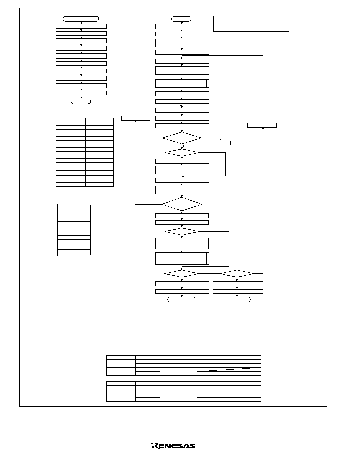
Rev. 2.0, 04/02, page 763 of 906
Start
End of programming
End sub
Set SWE bit in FLMCR1
Wait (x) ms
n = 1
m = 0
Sub-routine-call
Sub-routine-call
See Note 7 for pulse width
Note 7: Write Pulse Width
Start of programming
Write pulse application
Set PSU bit in FLMCR1
Enable WDT
Set P bit in FLMCR1
Wait (y)
µ
s
Clear P bit in FLMCR1
Wait (z1) ms or (z2) ms or (z3) ms
Clear PSU bit in FLMCR1
Wait (
) ms
Disable WDT
Wait (
) ms
Write pulse application subroutine
NG
NG
NG
NG
NG
NG
OK
OK
OK
OK
OK
Wait (
) ms
Wait (
) ms
*
2
*
4
*
6
*
6
*
6
*
6
*
6
*
6
*
6
*
5
*
6
*
6
*
1
Set PV bit in FLMCR1
H'FF dummy write to verify address
Read verify data
Additional program data computation
Transfer additional program data to
additional program data area
Write data = verify
data?
*
4
*
1
*
4
*
3
Reprogram data computation
Clear PV bit in FLMCR1
Clear SWE bit in FLMCR1
m = 1
128-byte
data verification
completed?
m = 0?
6
n ?
6
n ?
Increment address
Programming failure
OK
Clear SWE bit in FLMCR1
n
(N)?
Reprogram Data (X')
0
1
Verify Data (V)
0
1
0
1
Additional Program Data (Y)
0
1
Comments
Additional programming executed
Additional programming not executed
Additional programming not executed
Additional programming not executed
Additional Program Data Operation Chart
Write 128-byte data in RAM reprogram
data area consecutively to flash memory
Write pulse application
(z1)
µ
s or (z2)
µ
s
Perform programming in the erased state.
Do not perform additional programming
on previously programmed addresses.
RAM
Program data storage
area (128 bytes)
Reprogram data storage
area (128 bytes)
Additional program data
storage area (128 bytes)
Store 128-byte program data in program
data area and reprogram data area
Number of Writes (n)
1
2
3
4
5
6
7
8
9
10
11
12
13
.
.
.
998
999
1000
Write Time (z) ms
z1
z1
z1
z1
z1
z1
z2
z2
z2
z2
z2
z2
z2
.
.
.
z2
z2
z2
Notes: 1. Data transfer is performed by byte transfer. The lower 8 bits of the first address written to must be H'00 or H'80. A 128-byte data transfer must
be performed even if writing fewer than 128 bytes; in this case, H'FF data must be written to the extra addresses.
2. Verify data is read in 16-bit (W) units.
3. The reprogram data is given by the operation of the following tables (comparison between stored data in the program data area and verify data).
Programming is executed for the bits of reprogram data 0 in the next reprogram loop. Even bits for which programming has been completed will
be subjected to additional programming if they fail the subsequent verify operation.
4. A 128-byte areas for storing program data, reprogram data, and additional program data must be provided in the RAM. The contents of the
reprogram and additional program data are modified as programming proceeds.
5. A write pulse of (z1) or (z2) µs should be applied according to the progress of the programming operation. See Note 7 for the pulse widths.
When writing of additional-programming data is executed, a (z3)
µ
s write pulse should be applied.
Reprogram data X' means reprogram data when the write pulse is applied.
6. For the values of x, y, z1, z2, z3, a, b, g, e, h, q, and N, see section 24.6, Flash Memory Characteristics.
Original Data (D)
0
1
Verify Data (V)
0
1
0
1
Reprogram Data (X)
1
0
1
Comments
Programming completed
Programming incomplete; reprogram
Still in erased state; no action
Program Data Operation Chart
Transfer reprogram data to reprogram
data area
n ¨ n + 1
Note: Use a z3 µs write pulse for additional
programming.
Sequentially write 128-byte data in
additional program data area in RAM to
flash memory
Write pulse application
(z3) µs
(additional programming)
Wait (
) ms
Wait (
) ms
Wait (
) ms
Figure 19.10 Program/Program-Verify Flowchart

Rev. 2.0, 04/02, page 764 of 906
19.8.2
Erase/Erase-Verify
When erasing flash memory, the erase/erase-verify flowchart shown in figure 19.11 should be
followed.
1. Prewriting (setting erase block data to all 0s) is not necessary.
2. Erasing is performed in block units. Make only a single-bit specification in the erase block
registers (EBR1 and EBR2). To erase multiple blocks, each block must be erased in turn.
3. The time during which the E bit is set to 1 is the flash memory erase time.
4. The watchdog timer (WDT) is set to prevent overprogramming due to program runaway, etc.
Set a value greater than (y + z +
+
) ms as the WDT overflow period.
5. For a dummy write to a verify address, write 1-byte data H'FF to an address whose lower two
bits are B'00. Verify data can be read in longwords from the address to which a dummy write
was performed.
6. If the read data is unerased, set erase mode again, and repeat the erase/erase-verify sequence as
before. The maximum number of repetitions of the erase/erase-verify sequence (N) must not
be exceeded.
19.8.3
Interrupt Handling when Programming/Erasing Flash Memory
All interrupts, including NMI input, are disabled when flash memory is being programmed or
erased, and while the boot program is executing in boot mode. There are three reasons for this:
1. Interrupt during programming or erasing might cause a violation of the programming or
erasing algorithm, with the result that normal operation could not be assured.
2. If the interrupt exception handling is started when the vector address has not been programmed
yet or the flash memory is being programmed or erased, the vector would not be read correctly,
possibly resulting in CPU runaway.
3. If an interrupt occurred during boot program execution, it would not be possible to execute the
normal boot mode sequence.
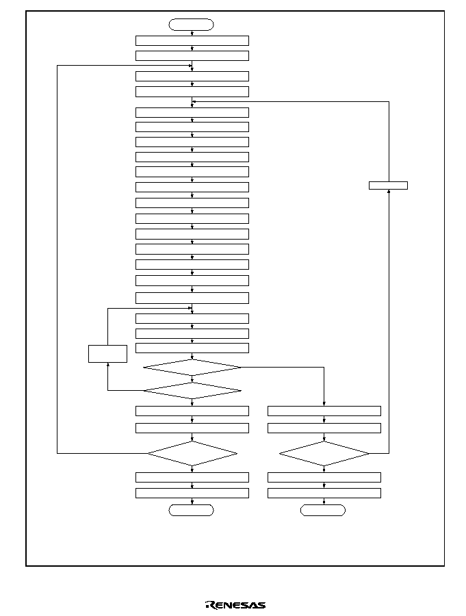
Rev. 2.0, 04/02, page 765 of 906
End of erasing
Start
Set SWE bit in FLMCR1
Set ESU bit in FLMCR1
Set E bit in FLMCR1
Wait (x)
µ
s
Wait (y)
µ
s
n = 1
Set EBR1, EBR2
Enable WDT
2
2
4
Wait (z) ms
2
Wait (
)
µ
s
2
Wait (
)
µ
s
2
Wait (
)
µ
s
Set block start address to verify address
2
Wait (
)
µ
s
2
3
2
2
2
Wait (
)
µ
s
2
2
5
Start of erase
Clear E bit in FLMCR1
Clear ESU bit in FLMCR1
Set EV bit in FLMCR1
H'FF dummy write to verify address
Read verify data
Clear EV bit in FLMCR1
Wait (
)
µ
s
Clear EV bit in FLMCR1
Clear SWE bit in FLMCR1
Disable WDT
Halt erase
1
Verify data = all 1?
Last address of block?
End of
erasing of all erase
blocks?
Erase failure
Clear SWE bit in FLMCR1
n
N?
NG
NG
NG
NG
OK
OK
OK
OK
n ¨ n + 1
Increment
address
Notes: 1. Prewriting (setting erase block data to all 0) is not necessary.
2. The values of x, y, z,
,
,
,
,
,
, and N are shown in section 24.6, Flash Memory Characteristics.
3. Verify data is read in 16-bit (W) units.
4. Set only one bit in EBR1or EBR2. More than one bit cannot be set.
5. Erasing is performed in block units. To erase a number of blocks, the individual blocks must be erased sequentially.
Wait (
)
µ
s
Wait (
)
µ
s
Figure 19.11 Erase/Erase-Verify Flowchart

Rev. 2.0, 04/02, page 766 of 906
19.9
Program/Erase Protection
There are three kinds of flash memory program/erase protection: hardware protection, software
protection, and error protection.
19.9.1
Hardware Protection
Hardware protection refers to a state in which programming/erasing of flash memory is forcibly
disabled or aborted because of a transition to reset (including an overflow reset by the WDT) or
standby mode. Flash memory control register 1 (FLMCR1), flash memory control register 2
(FLMCR2), erase block register 1 (EBR1), and erase block register 2 (EBR2) are initialized. In a
reset via the
#$ pin, the reset state is not entered unless the #$ pin is held low until oscillation
stabilizes after powering on. In the case of a reset during operation, hold the
#$ pin low for the
#$ pulse width specified in the AC Characteristics section.
19.9.2
Software Protection
Software protection can be implemented against programming/erasing of all flash memory blocks
by clearing the SWE bit in FLMCR1 (this operation must be executed in the on-chip RAM or
external memory). When software protection is in effect, setting the P or E bit in FLMCR1 does
not cause a transition to program mode or erase mode. By setting the erase block register 1
(EBR1) and erase block register 2 (EBR2), erase protection can be set for individual blocks.
When EBR1 and EBR2 are set to H'00, erase protection is set for all blocks.
19.9.3
Error Protection
In error protection, an error is detected when the CPU's runaway occurs during flash memory
programming/erasing, or operation is not performed in accordance with the program/erase
algorithm, and the program/erase operation is forcibly aborted. Aborting the program/erase
operation prevents damage to the flash memory due to overprogramming or overerasing.
When the following errors are detected during programming/erasing of flash memory, the FLER
bit in FLMCR2 is set to 1, and the error protection state is entered.
∑
When flash memory is read during programming/erasing (including a vector read or instruction
fetch)
∑
When an exception handling (excluding a reset) is started during programming/erasing
∑
When a SLEEP instruction is executed during programming/erasing
∑
When the CPU releases the bus mastership during programming/erasing
The FLMCR1, FLMCR2, EBR1, and EBR2 settings are retained, but program mode or erase
mode is forcibly aborted at the point at which the error occurred. Program mode or erase mode
cannot be re-entered by re-setting the P or E bit. However, PV and EV bit setting is enabled, and a

Rev. 2.0, 04/02, page 767 of 906
transition can be made to verify mode. The error protection state can be canceled by a power-on
reset or in hardware standby mode.
19.10
Programmer Mode
In programmer mode, a PROM programmer can perform programming/erasing via a socket
adapter, just like for a discrete flash memory. Use a PROM programmer which supports the
Hitachi 512-kbyte flash memory on-chip MCU device type (FZTAT512V3A). A 12-MHz input
clock is needed.
19.11
Power-Down States for Flash Memory
In user mode, the flash memory will operate in either of the following states:
∑
Normal operating mode
The flash memory can be read.
∑
Standby mode
All flash memory circuits are halted.
Table 19.7 shows the correspondence between the operating modes of this LSI and the flash
memory. When the flash memory returns to normal operation from a standby state, a power
supply circuit stabilization period is needed. When the flash memory returns to its normal
operating state, bits STS3 to STS0 in SBYCR must be set to provide a wait time of at least 100 µs,
even when the external clock is being used.
Table 19.7
Flash Memory Operating States
Operating Mode
Flash Memory Operating State
Active mode
Normal operating state
Sleep mode
Normal operating state
Standby mode
Standby state
19.12
Usage Notes
Precautions concerning the use of on-board programming mode, the RAM emulation function, and
programmer mode are summarized below.
1. Use the specified voltages and timing for programming and erasing.
Applied voltages in excess of the rating can permanently damage the device. Use a PROM
programmer that supports the Hitachi microcomputer device type with 512-kbyte on-chip flash
memory (FZTAT512V3A).

Rev. 2.0, 04/02, page 768 of 906
Do not select the HN27C4096 setting for the PROM programmer, and only use the specified
socket adapter.
2. Reset the flash memory before turning on/off the power.
When applying or disconnecting Vcc power, fix the
#$ pin low and place the flash memory
in the hardware protection state. The power-on and power-off timing requirements should also
be satisfied in the event of a power failure and subsequent recovery.
3. Powering on and off.
Do not apply a high level to the FWE pin until V
CC
has stabilized. Also, drive the FWE pin low
before turning off V
CC
.
When applying or disconnecting V
CC
power, fix the FWE pin low and place the flash memory
in the hardware protection state.
The power-on and power-off timing requirements should also be satisfied in the event of a
power failure and subsequent recovery. The power-on and power-off timing in the H8S/2678
Series is shown in figure 19.12.
4. FWE application/disconnection.
FWE application should be carried out when this LSI operation is in a stable condition. If this
LSI operation is not stable, fix the FWE pin low and set the protection state.
The following points must be observed concerning FWE application and disconnection to prevent
unintentional programming or erasing of flash memory:
∑
Apply FWE when the V
CC
voltage has stabilized within its rated voltage range.
∑
In boot mode, apply and disconnect FWE during a reset.
∑
In user program mode, FWE can be switched between high and low level regardless of the
reset state. FWE input can also be switched during execution of a program in flash memory.
∑
Do not apply FWE if program runaway has occurred.
∑
Disconnect FWE only when the SWE, ESU, PSU, EV, PV, and E bits in FLMCR1 are cleared.
5. Do not apply a constant high level to the FWE pin.
Apply a high level to the FWE pin only when programming or erasing flash memory. Also,
while a high level is applied to the FWE pin, the watchdog timer should be activated to prevent
overprogramming or overerasing due to program runaway, etc.
6. Use the recommended algorithm when programming and erasing flash memory.
The recommended algorithm enables programming and erasing to be carried out without
subjecting the device to voltage stress or sacrificing program data reliability. When setting the
P or E bit in FLMCR1, the watchdog timer should be set beforehand as a precaution against
program runaway, etc.
7. Do not set or clear the SWE bit during execution of a program in flash memory.
Wait for at least 100 µs after clearing the SWE bit before executing a program or reading data
in flash memory.

Rev. 2.0, 04/02, page 769 of 906
When the SWE bit is set, data in flash memory can be rewritten. When the SWE bit is set to 1,
data in flash memory can be read only in program-verify/erase-verify mode. Access flash
memory only for verify operations (verification during programming/erasing). Also, do not
clear the SWE bit during programming, erasing, or verifying. Similarly, when using the RAM
emulation function, the SWE bit must be cleared before executing a program or reading data in
flash memory.
However, the RAM area overlapping flash memory space can be read and written to regardless
of whether the SWE bit is set or cleared.
8. Do not use interrupts while flash memory is being programmed or erased.
All interrupt requests, including NMI, should be disabled during programming/erasing the
flash memory to give priority to program/erase operations.
9. Do not perform additional programming. Erase the memory before reprogramming.
In on-board programming, perform only one programming operation on a 128-byte
programming unit block. In programmer mode, too, perform only one programming operation
on a 128-byte programming unit block. Programming should be carried out with the entire
programming unit block erased.
10. Before programming, check that the chip is correctly mounted in the PROM programmer.
Overcurrent damage to the device can result if the index marks on the PROM programmer
socket, socket adapter, and chip are not correctly aligned.
11. Do not touch the socket adapter or chip during programming.
Touching either of these can cause contact faults and write errors.
12. Apply the reset signal after the SWE, bit is cleared during its operation.
The reset signal is applied at least 100 µs after the SWE bit has been cleared.
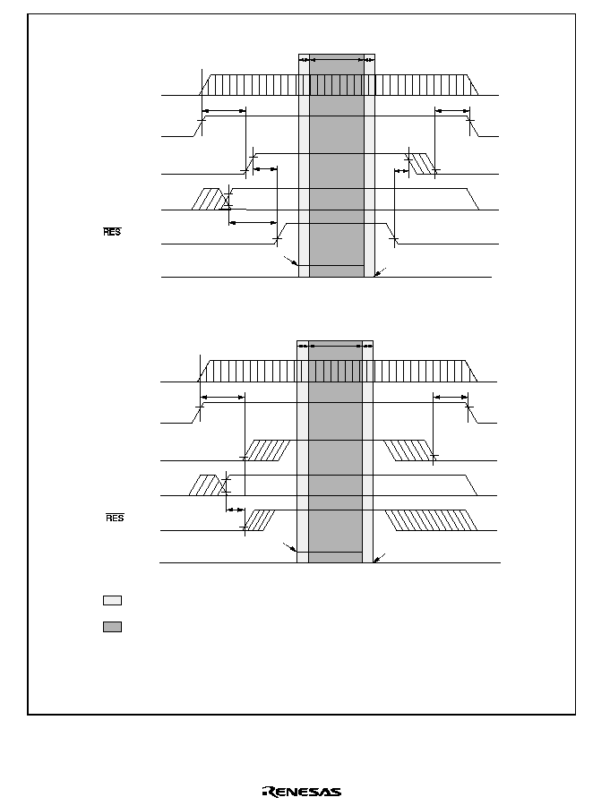
Rev. 2.0, 04/02, page 770 of 906
Period during which flash memory access is prohibited
(x: Wait time after setting SWE bit)
*
2
Period during which flash memory can be programmed
(Execution of program in flash memory prohibited, and data reads other than verify operations
prohibited)
¯
VCC
FWE
t
OSC1
Min 0
µ
s
Min 0
µ
s
t
MDS
*
3
t
MDS
*
3
MD2 to MD0
*
1
SWE bit
SWE set
SWE cleared
Programming/
erasing
possible
Wait time: x
Wait time: 100
µ
s
Notes: 1. Except when switching modes, the level of the mode pins (MD2 to MD0) must be fixed until
power-off by pulling the pins up or down.
2. See section 24.6, Flash Memory Characteristics.
3. Mode programming setup time t
MDS
(min) = 200 ns
SWE set
SWE cleared
¯
VCC
FWE
t
OSC1
Min 0
µ
s
MD2 to MD0
*
1
SWE bit
(2) User Program Mode
(1) Boot Mode
Programming/
erasing
possible
Wait time: x
Wait time: 100
µ
s
t
MDS
*
3
Figure 19.12 Power-On/Off Timing (H8S/2678 Series)
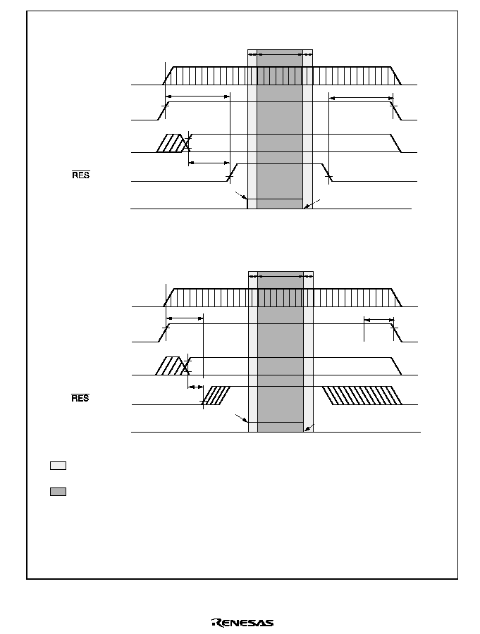
Rev. 2.0, 04/02, page 771 of 906
V
CC
t
OSC1
Min 0
µ
s
t
MDS
*
3
MD2 to MD0
*
1
SWE bit
SWE set
(1) Boot Mode
(2) User Program Mode
SWE cleared
Programming/
erasing
possible
Wait time: x
Wait time: 100
µ
s
Period during which flash memory access is prohibited
(x: Wait time after setting SWE bit)
*
2
Period during which flash memory can be programmed
(Execution of program in flash memory prohibited, and data reads other than verify operations
prohibited)
Notes: 1. Except when switching modes, the level of the mode pins (MD2 to MD0) must be fixed until
power-off by pulling the pins up or down.
2. See section 24.6, Flash Memory Characteristics.
3. Mode programming setup time t
MDS
(min) = 200 ns
SWE set
SWE cleared
V
CC
t
OSC1
MD2 to MD0
*
1
SWE bit
Programming/
erasing
possible
Wait time: x
t
MDS
*
3
Wait time: 100
µ
s
Min 0
µ
s
Figure 19.13 Power-On/Off Timing (H8S/2678R Series)
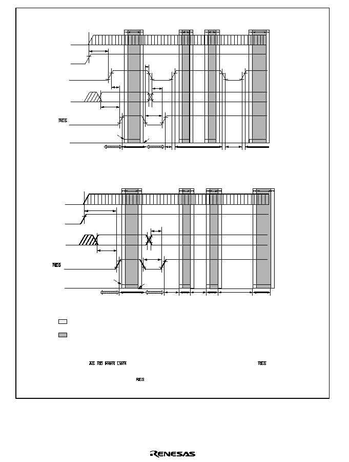
Rev. 2.0, 04/02, page 772 of 906
Period during which flash memory access is prohibited
(x: Wait time after setting SWE bit)
*
3
Period during which flash memory can be programmed
(Execution of program in flash memory prohibited, and data reads other than verify operations prohibited)
V
CC
FWE
t
OSC1
Min 0
µ
s
t
MDS
t
MDS
t
MDS
*
2
t
RESW
MD2 to MD0
SWE bit
Mode
change
*
1
Mode
change
*
1
Boot
mode
User
mode
User program mode
(1) H8S/2678 Series
(2) H8S/2678R Series
SWE
set
SWE
cleared
Programming/erasing
possible
Wait time: x
Programming/erasing
possible
Wait time: x
Programming/erasing
possible
Wait time: x
Programming/erasing
possible
Wait time: x
User
mode
User program
mode
Notes: 1. When entering boot mode or making a transition from boot mode to another mode, mode switching must be
carried out by means of RES input. The state of ports with multiplexed address functions and bus control output
pins (
,
,
,
) will change during this switchover interval (the interval during which the
pin
input is low), and therefore these pins should not be used as output signals during this time.
2. When making a transition from boot mode to another mode, a mode programming setup time t
MDS
(min) of 200
ns is necessary with respect to
clearance timing.
3. See section 24.6, Flash Memory Characteristics.
4. Wait time: 100
µ
s
V
CC
t
OSC1
t
MDS
t
MDS
Wait time: x
Programming/erasing
possible
Wait time: x
Programming/erasing
possible
Wait time: x
Programming/erasing
possible
Wait time: x
Programming/erasing
possible
t
RESW
MD2 to MD0
SWE bit
Boot
mode
Mode
change
*
1
Mode
change
*
1
User
program
mode
User
program
mode
User
program
mode
User mode
User
mode
User
mode
SWE
set
SWE
cleared
*
4
*
4
*
4
*
2
Figure 19.14 Mode Transition Timing
(Example: Boot Mode
User Mode
User Program Mode)

Rev. 2.0, 04/02, page 773 of 906
19.13
Note on Switching from F-ZTAT Version to Masked ROM Version
Care is required if application software developed on the F-ZTAT version is used when the F-
ZTAT version is switched to the masked ROM version product.
If an address in which a register for the F-ZTAT version is present is read (see section 23.1,
Register Addresses) in the masked ROM version, an undefined value will be returned.
If application software developed on the F-ZTAT version is used in the masked ROM version
product, the state of the FWE pin cannot be judged. The program must be modified so that the part
of reprogramming (erasing/programming) the flash memory and the part of the RAM emulation
are not started.
Also, the mode pin of boot mode must not be set in the masked ROM version.
Note:
This note is applied to all products in the F-ZTAT version and in the masked ROM
version of same series with the different ROM size.

Rev. 2.0, 04/02, page 774 of 906
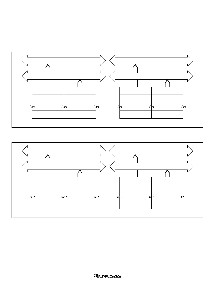
Rev. 2.0, 04/02, page 775 of 906
Section 20 Masked ROM
This series microcomputer has 64, 128, or 256 kbytes of on-chip masked ROM. The on-chip ROM
is connected to the CPU, data transfer controller (DTC), and DMA controller (DMAC) with a 16-
bit data bus. The on-chip ROM can be accessed by the CPU, DTC, and DMAC in 8 or 16-bit
units. The data in the on-chip ROM can always be accessed in one state.
H'000000
H'000002
H'03FFFE
H'000001
H'000003
H'03FFFF
Internal data bus (upper 8 bits)
Modes 4 and 7
Modes 5 and 6
Internal data bus (lower 8 bits)
H'100000
H'100002
H'13FFFE
H'100001
H'100003
H'13FFFF
Internal data bus (upper 8 bits)
Internal data bus (lower 8 bits)
Figure 20.1 Block Diagram of 256-Kbyte Masked ROM (HD6432676)
H'000000
H'000002
H'01FFFE
H'000001
H'000003
H'01FFFF
Internal data bus (upper 8 bits)
Modes 4 and 7
Modes 5 and 6
Internal data bus (lower 8 bits)
H'100000
H'100002
H'11FFFE
H'100001
H'100003
H'11FFFF
Internal data bus (upper 8 bits)
Internal data bus (lower 8 bits)
Figure 20.2 Block Diagram of 128-Kbyte Masked ROM (HD6432675)
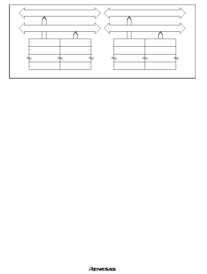
Rev. 2.0, 04/02, page 776 of 906
H'000000
H'000002
H'00FFFE
H'000001
H'000003
H'00FFFF
Internal data bus (upper 8 bits)
Modes 4 and 7
Modes 5 and 6
Internal data bus (lower 8 bits)
H'100000
H'100002
H'10FFFE
H'100001
H'100003
H'10FFFF
Internal data bus (upper 8 bits)
Internal data bus (lower 8 bits)
Figure 20.3 Block Diagram of 64-Kbyte Masked ROM (HD6432673)
The operating mode enables or disables the on-chip ROM. The operating mode is selected by the
mode setting pins, such as the FWE and MD3 to MD0 pins as shown in table 3.1. Select modes 4
to 7 when the on-chip ROM is used, and mode 1 or 2 when the on-chip ROM is not used. The on-
chip ROM is allocated in area 0.
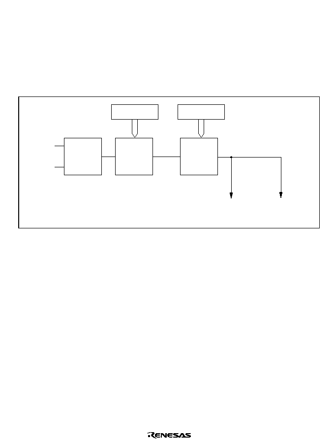
Rev. 2.0, 04/02, page 777 of 906
Section 21 Clock Pulse Generator
This LSI has an on-chip clock pulse generator (CPG) that generates the system clock (¯) and
internal clocks.
The clock pulse generator consists of an oscillator circuit, PLL circuit, and divider.
Figure 21.1 shows a block diagram of the clock pulse generator.
EXTAL
PLL circuit
(
◊
1, 2, 4)
Oscillator
Divider
System clock
to ¯ pin
Internal clock
to peripheral
modules
SCK2 to SCK0
SCKCR
STC0, STC1
PLLCR
XTAL
Legend
PLLCR: PLL system control register
SCKCR: System clock control register
Figure 21.1 Block Diagram of Clock Pulse Generator
The frequency can be changed by means of the PLL circuit. Frequency changes are made by
software by means of settings in the PLL control register (PLLCR) and the system clock control
register (SCKCR).
21.1
Register Descriptions
The clock pulse generator has the following registers.
∑
System clock control register (SCKCR)
∑
PLL control register (PLLCR)
21.1.1
System Clock Control Register (SCKCR)
SCKCR controls ¯ clock output and selects operation when the frequency multiplication factor
used by the PLL circuit is changed, and the division ratio used by the divider.
CPG0400A_010020020400

Rev. 2.0, 04/02, page 778 of 906
Bit
Bit Name
Initial Value
R/W
Description
7
PSTOP
0
R/W
¯ Clock Output Disable
Controls ¯ output.
Normal Operation
0: ¯ output
1: Fixed high
Sleep Mode
0: ¯ output
1: Fixed high
Software Standby Mode
0: Fixed high
1: Fixed high
Hardware Standby Mode
0: High impedance
1: High impedance
All module clock stop mode
0: ¯ output
1: Fixed high
6
--
0
R/W
Reserved
This bit can be read from or written to. However, The
write value should always be 0.
5
4
--
--
0
0
R/W
R/W
Reserved
These bits are always read as 0. However, the write
value should always be 0.
3
STCS
0
R/W
Frequency Multiplication Factor Switching Mode Select
Selects the operation when the PLL circuit frequency
multiplication factor is changed.
0: Specified multiplication factor is valid after transition
to software standby mode
1: Specified multiplication factor is valid immediately
after STC1 and STC0 bits are rewritten

Rev. 2.0, 04/02, page 779 of 906
Bit
Bit Name
Initial Value
R/W
Description
2
1
0
SCK2
SCK1
SCK0
0
0
0
R/W
R/W
R/W
System Clock Select 2 to 0
Select the division ratio.
000: 1/1
001: 1/2
010: 1/4
011: 1/8
100: 1/16
101: 1/32
11X: Setting prohibited
X: Don't care
21.1.2
PLL Control Register (PLLCR)
PLLCR sets the frequency multiplication factor used by the PLL circuit.
Bit
Bit Name
Initial Value
R/W
Description
7
to
4
--
0
--
Reserved
These bits are always read as 0 and cannot be
modified.
3
--
0
R/W
Reserved
This bit can be read from or written to. However,
the write value should always be 0.
2
--
0
R/W
Reserved
This bit is always read as 0 and cannot be
modified.
1
0
STC1
STC0
0
0
R/W
R/W
Frequency Multiplication Factor
The STC bits specify the frequency multiplication
factor used by the PLL circuit.
00:
◊
1
01:
◊
2
10:
◊
4
11: Setting prohibited
21.2
Oscillator
Clock pulses can be supplied by connecting a crystal resonator, or by input of an external clock.
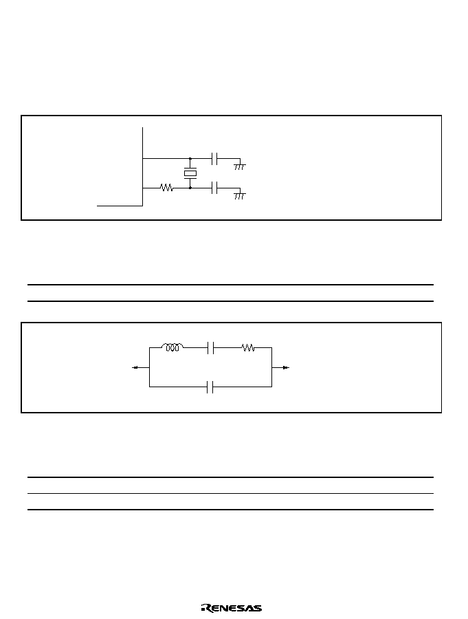
Rev. 2.0, 04/02, page 780 of 906
21.2.1
Connecting a Crystal Resonator
A crystal resonator can be connected as shown in the example in figure 21.2. Select the damping
resistance R
d
according to table 20.1. An AT-cut parallel-resonance type should be used.
Figure 21.3 shows the equivalent circuit of the crystal resonator. Use a crystal resonator that has
the characteristics shown in table 21.2.
EXTAL
XTAL
R
d
C
L2
C
L1
C
L1
= C
L2
= 10 to 22 pF
Figure 21.2 Connection of Crystal Resonator (Example)
Table 21.1
Damping Resistance Value
Frequency (MHz)
8
12
16
20
25
R
d
(
)
200
0
0
0
0
XTAL
C
L
AT-cut parallel-resonance type
EXTAL
C
0
L
R
s
Figure 21.3 Crystal Resonator Equivalent Circuit
Table 21.2
Crystal Resonator Characteristics
Frequency (MHz)
8
12
16
20
25
R
S
max (
)
80
60
50
40
40
C
0
max (pF)
7
7
7
7
7
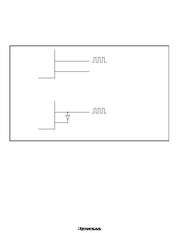
Rev. 2.0, 04/02, page 781 of 906
21.2.2
External Clock Input
An external clock signal can be input as shown in the examples in figure 21.4. If the XTAL pin is
left open, make sure that parasitic capacitance is no more than 10 pF. When the counter clock is
input to the XTAL pin, make sure that the external clock is held high in standby mode.
Table 21.3 shows the input conditions for the external clock
EXTAL
XTAL
External clock input
Open
(a) XTAL pin left open
EXTAL
XTAL
External clock input
(b) Counter clock input at XTAL pin
Figure 21.4 External Clock Input (Examples)
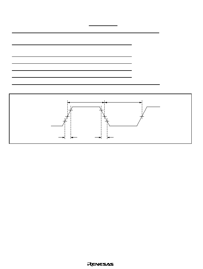
Rev. 2.0, 04/02, page 782 of 906
Table 21.3
External Clock Input Conditions
V
CC
= 3.0 V
to 3.6 V
Test
Item
Symbol
Min
Max
Unit
Conditions
External clock input
low pulse width
t
EXL
15
--
ns
Figure 21.5
External clock input
high pulse width
t
EXH
15
--
ns
External clock rise time
t
EXr
--
5
ns
External clock fall time
t
EXf
--
5
ns
Clock low pulse width
t
CL
0.4
0.6
t
cyc
Clock high pulse width
t
CH
0.4
0.6
t
cyc
t
EXH
t
EXL
t
EXr
t
EXf
V
CC
◊
0.5
EXTAL
Figure 21.5 External Clock Input Timing
21.3
PLL Circuit
The PLL circuit has the function of multiplying the frequency of the clock from the oscillator by a
factor of 1, 2, or 4. The multiplication factor is set with the STC1 and the STC0 bits in PLLCR.
The phase of the rising edge of the internal clock is controlled so as to match that of the rising
edge of the EXTAL pin.
When the multiplication factor of the PLL circuit is changed, the operation varies according to the
setting of the STCS bit in SCKCR.
When STCS = 0, the setting becomes valid after a transition to software standby mode. The
transition time count is performed in accordance with the setting of bits STS3 to STS0 in SBYCR.
For details on SBYCR, refer to section 22.1.1, Standby Control Register (SBYCR).
1. The initial PLL circuit multiplication factor is 1.
2. A value is set in bits STS3 to STS0 to give the specified transition time.

Rev. 2.0, 04/02, page 783 of 906
3. The target value is set in bits STC1 and STC0, and a transition is made to software standby
mode.
4. The clock pulse generator stops and the value set in STC1 and STC0 becomes valid.
5. Software standby mode is cleared, and a transition time is secured in accordance with the
setting in STS3 to STS0.
6. After the set transition time has elapsed, this LSI resumes operation using the target
multiplication factor.
When STCS = 1, this LSI operates using the new multiplication factor immediately after bits
STC1 and STC0 are rewritten.
21.4
Frequency Divider
The frequency divider divides the PLL output clock to generate a 1/2, 1/4, 1/8, 1/16, or 1/32 clock.
21.5
Usage Notes
21.5.1
Notes on Clock Pulse Generator
1. The following points should be noted since the frequency of
changes according to the
setting of SCKCR and PLLCR.
Select the clock division ratio that is within the operation guaranteed range of clock cycle time
tcyc shown in the AC timing of Electrical Characteristics. In other words, the range of
must
be specified from 8 MHz (min) to 33 MHz (max); outside of this range must be prevented.
2. All the on-chip peripheral modules operate on the
. Therefore, note that the time processing
of modules such as a timer and SCI differ before and after changing the clock division ratio. In
addition, wait time for clearing software standby mode differs by changing the clock division
ratio. See the description, Setting Oscillation Stabilization Time after Clearing Software
Standby Mode in section 22.2.3, Software Standby Mode, for details.
3. Note that the frequency of
will be changed when setting SCKCR or PLLCR while executing
the external bus cycle with the write-data-buffer function or the EXDMAC.
21.5.2
Notes on Resonator
Since various characteristics related to the resonator are closely linked to the user's board design,
thorough evaluation is necessary on the user's part, using the oscillator connection examples
shown in this section as a guide. As the parameters for the oscillation circuit will depend on the
floating capacitance of the resonator and the user board, the parameters should be determined in
consultation with the resonator manufacturer. The design must ensure that a voltage exceeding the
maximum rating is not applied to the oscillator pin.

Rev. 2.0, 04/02, page 784 of 906
21.5.3
Notes on Board Design
When using the crystal resonator, place the crystal resonator and its load capacitors as close as
possible to the XTAL and EXTAL pins. Other signal lines should be routed away from the
oscillation circuit to prevent induction from interfering with correct oscillation. See figure 21.6.
C
L2
Signal A Signal B
C
L1
This LSI
XTAL
EXTAL
Avoid
Figure 21.6 Note on Board Design for Oscillation Circuit
Figure 21.7 shows the external circuitry recommended for the PLL circuit. Separate PLLVcc and
PLLVss from the other Vcc and Vss lines at the board power supply source, and be sure to insert
bypass capacitors CPB and CB close to the pins.
PLLV
CC
PLLV
SS
V
CC
V
SS
Rp: 200
CPB: 0.1 µF
*
CB: 0.1 µF
*
Note:
*
CB and CPB are laminated ceramic capacitors.
Figure 21.7 Recommended External Circuitry for PLL Circuit

Rev. 2.0, 04/02, page 785 of 906
Section 22 Power-Down Modes
In addition to the normal program execution state, this LSI has power-down modes in which
operation of the CPU and oscillator is halted and power dissipation is reduced. Low-power
operation can be achieved by individually controlling the CPU, on-chip peripheral modules, and
so on.
This LSI's operating modes are high-speed mode and six power down modes:
∑
Clock division mode
∑
Sleep mode
∑
Module stop mode
∑
All module clock stop mode
∑
Software standby mode
∑
Hardware standby mode
Sleep mode is a CPU state, clock division mode is a CPU and bus master state, and module stop
mode is an on-chip peripheral function (including bus masters other than the CPU) state. A
combination of these modes can be set.
After a reset, this LSI is in high-speed mode.
Table 22.1 shows the internal states of this LSI in each mode. Figure 21.1 shows the mode
transition diagram.
LPWS261A_010020020400

Rev. 2.0, 04/02, page 786 of 906
Table 22.1
Operating Modes
Operating State
High
Speed
Mode
Clock
Division
Mode
Sleep
Mode
Module
Stop Mode
All Module
Clock Stop
Mode
Software
Standby
Mode
Hardware
Standby
Mode
Clock pulse generator
Functions
Functions
Functions
Functions
Functions
Halted
Halted
Instruction
execution
Halted
Halted
Halted
CPU
Register
Functions
Functions
Retained
Functions
Halted
Retained
Undefined
NMI
External
interrupts
IRQ0 to 15
Functions
Functions
Functions
Functions
Functions
Functions
Halted
Peripheral
functions
WDT
Functions
Functions
Functions
Functions
Functions
Halted
(Retained)
Halted
(Reset)
TMR
Functions
Functions
Functions
Halted
(Retained)
Functions/
Halted
(Retained)
*
Halted
(Retained)
Halted
(Reset)
EXDMAC
Functions
Functions
Functions
Halted
(Retained)
Halted
(Retained)
Halted
(Retained)
Halted
(Reset)
DMAC
Functions
Functions
Functions
Halted
(Retained)
Halted
(Retained)
Halted
(Retained)
Halted
(Reset)
DTC
Functions
Functions
Functions
Halted
(Retained)
Halted
(Retained)
Halted
(Retained)
Halted
(Reset)
TPU
Functions
Functions
Functions
Halted
(Retained)
Halted
(Retained)
Halted
(Retained)
Halted
(Reset)
PPG
Functions
Functions
Functions
Halted
(Retained)
Halted
(Retained)
Halted
(Retained)
Halted
(Reset)
D/A
Functions
Functions
Functions
Halted
(Retained)
Halted
(Retained)
Halted
(Retained)
Halted
(Reset)
A/D
Functions
Functions
Functions
Halted
(Retained)
Halted
(Retained)
Halted
(Reset)
Halted
(Reset)
SCI
Functions
Functions
Functions
Halted
(Reset)
Halted
(Reset)
Halted
(Reset)
Halted
(Reset)
RAM
Functions
Functions
Functions
Functions
Functions
Retained
Retained
I/O
Functions
Functions
Functions
Functions
Retained
Retained
High
impedance
Notes: "Halted (Retained)" in the table means that internal register values are retained and internal
operations are suspended.
"Halted (Reset)" in the table means that internal register values and internal states are
initialized.
In module stop mode, only modules for which a stop setting has been made are halted
(reset or retained).
*
The active or halted state can be selected by means of the MSTP0 bit in MSTPCR.
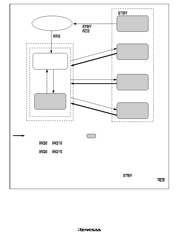
Rev. 2.0, 04/02, page 787 of 906
Program-halted state
Program execution state
High-speel mode
(Internal clock is PLL
circuit output clock)
Reset state
pin = low
pin = high
pin = low
SSBY = 0
MSTPCR =
H'FFFF (H'FFFE),
SSBY = 0
SSBY = 1
SCK2 to
SCK0
0
pin = high
SCK2 to
SCK0 = 0
SLEEP
instruction
Interrupt
*
1
: Transition after exception handling
: Power- down mode
SLEEP
instruction
Any interrupt
SLEEP
instruction
External
interrupt
*
2
Notes: 1. NMI,
to
, 8-bit timer interrupts, watchdog timer interrupts.
(8-bit timer interrupts are valid when MSTP0 = 0.)
2. NMI,
to
(IRQ0 to IRQ15 are valid when the corresponding bit in SSIER is 1.)
∑ When a transition is made between modes by means of an interrupt, the transition cannot be
made on interrupt source generation alone. Ensure that interrupt handling is performed after
accepting the interrupt request.
∑ From any state, a transition to hardware standby mode occurs when
is driven low.
∑ From any state except hardware standby mode, a transition to the reset state occurs when
is driven low.
Hardware
standby mode
Sleep mode
All
module-clocks-stop
mode
Software
standby mode
Clock division
mode
Figure 22.1 Mode Transitions

Rev. 2.0, 04/02, page 788 of 906
22.1
Register Descriptions
The registers relating to the power-down mode are shown below. For details on the system clock
control register (SCKCR), refer to section 21.1.1, System Clock Control Register (SCKCR).
∑
System clock control register (SCKCR)
∑
Standby control register (SBYCR)
∑
Module stop control register H (MSTPCRH)
∑
Module stop control register L (MSTPCRL)
22.1.1
Standby Control Register (SBYCR)
SBYCR performs software standby mode control.
Bit
Bit Name
Initial Value
R/W
Description
7
SSBY
0
R/W
Software Standby
This bit specifies the transition mode after
executing the SLEEP instruction
0: Shifts to sleep mode after the SLEEP instruction
is executed
1: Shifts to software standby mode after the SLEEP
instruction is executed
This bit does not change when clearing the
software standby mode by using external interrupts
and shifting to normal operation. This bit should be
written 0 when clearing.
6
OPE
1
R/W
Output Port Enable
Specifies whether the output of the address bus
and bus control signals (
&6
to
&6
,
$6
,
5'
,
+:5
,
/:5
,
8&$6
,
/&$6
) is retained or set to the
high-impedance state in software standby mode.
0: In software standby mode, address bus and bus
control signals are high-impedance
1: In software standby mode, address bus and bus
control signals retain output state

Rev. 2.0, 04/02, page 789 of 906
Bit
Bit Name
Initial Value
R/W
Description
5
4
--
--
0
0
--
--
Reserved
These bits are always read as 0.
The initial value
should not be changed.
3
2
1
0
STS3
STS2
STS1
STS0
1
1
1
1
R/W
R/W
R/W
R/W
Standby Timer Select 3 to 0
These bits select the time the MCU waits for the
clock to stabilize when software standby mode is
cleared by an external interrupt. With crystal
oscillation, refer to table 22.2 and make a selection
according to the operating frequency so that the
standby time is at least the oscillation stabilization
time. With an external clock, a PLL circuit
stabilization time is necessary. Refer to table 22.2
to set the wait time. When DRAM is used and self-
refreshing in the software standby state is selected,
note that the DRAM's tRAS (self-refresh RAS pulse
width) specification must be satisfied.
With the F-ZTAT version, a flash memory
stabilization time must be provided.
0000: Setting prohibited
0001: Setting prohibited
0010: Setting prohibited
0011: Setting prohibited
0100: Setting prohibited
0101: Standby time = 64 states
0110: Standby time = 512 states
0111: Standby time = 1024 states
1000: Standby time = 2048 states
1001: Standby time = 4096 states
1010: Standby time = 16384 states
1011: Standby time = 32768 states
1100: Standby time = 65536 states
1101: Standby time = 131072 states
1110: Standby time = 262144 states
1111: Standby time = 524288 states

Rev. 2.0, 04/02, page 790 of 906
22.1.2
Module Stop Control Registers H and L (MSTPCRH, MSTPCRL)
MSTPCR performs module stop mode control.
Setting a bit to 1, the corresponding module enters module stop mode, while clearing the bit to 0
clears the module stop mode.
MSTPCRH
Bit
Bit Name
Initial Value
R/W
Module
15
ACSE
0
R/W
All-Module-Clocks-Stop Mode Enable
Enables or disables all-module-clocks-stop mode,
in which, when the CPU executes a SLEEP
instruction after module stop mode has been set
for all the on-chip peripheral functions controlled by
MSTPCR or the on-chip peripheral functions
except the TMR.
0: All-module-clocks-stop mode disabled
1: All-module-clocks-stop mode enabled
14
MSTP14
0
R/W
EXDMA controller (EXDMAC)
13
MSTP13
0
R/W
DMA controller (DMAC)
12
MSTP12
0
R/W
Data transfer controller (DTC)
11
MSTP11
1
R/W
16-bit timer-pulse unit (TPU)
10
MSTP10
1
R/W
Programmable pulse generator (PPG)
9
MSTP9
1
R/W
D/A converter (channels 0 and 1)
8
MSTP8
1
R/W
D/A converter (channels 2 and 3)
MSTPCRL
Bit
Bit Name
Initial Value
R/W
Module
7
MSTP7
1
R/W
--
6
MSTP6
1
R/W
A/D converter
5
MSTP5
1
R/W
--
4
MSTP4
1
R/W
--
3
MSTP3
1
R/W
Serial communication interface 2 (SCI_2)
2
MSTP2
1
R/W
Serial communication interface 1 (SCI_1)
1
MSTP1
1
R/W
Serial communication interface 0 (SCI_0)
0
MSTP0
1
R/W
8-bit timer (TMR)

Rev. 2.0, 04/02, page 791 of 906
22.2
Operation
22.2.1
Clock Division Mode
When bits SCK2 to SCK0 in SCKCR are set to a value from 001 to 101, a transition is made to
clock division mode at the end of the bus cycle. In clock division mode, the CPU, bus masters, and
on-chip peripheral functions all operate on the operating clock (1/2, 1/4, 1/8, 1/16, or 1/32)
specified by bits SCK2 to SCK0.
Clock division mode is cleared by clearing all of bits SCK2 to SCK0 to 0. A transition is made to
high-speed mode at the end of the bus cycle, and clock division mode is cleared.
If a SLEEP instruction is executed while the SSBY bit in SBYCR is cleared to 0, the chip enters
sleep mode. When sleep mode is cleared by an interrupt, clock division mode is restored.
If a SLEEP instruction is executed while the SSBY bit in SBYCR is set to 1, the chip enters
software standby mode. When software standby mode is cleared by an external interrupt, clock
division mode is restored.
When the
5(6 pin is driven low, the reset state is entered and clock division mode is cleared. The
same applies to a reset caused by watchdog timer overflow.
When the
67%< pin is driven low, a transition is made to hardware standby mode.
22.2.2
Sleep Mode
Transition to Sleep Mode: When the SLEEP instruction is executed when the SSBY bit is 0 in
SBYCR, the CPU enters the sleep mode. In sleep mode, CPU operation stops but the contents of
the CPU's internal registers are retained. Other peripheral functions do not stop.
Exiting Sleep Mode: Sleep mode is exited by any interrupt, or signals at the
5(6, or 67%< pins.
∑
Exiting Sleep Mode by Interrupts:
When an interrupt occurs, sleep mode is exited and interrupt exception processing starts. Sleep
mode is not exited if the interrupt is disabled, or interrupts other than NMI are masked by the
CPU.
∑
Exiting Sleep Mode by
5(6 pin:
Setting the
5(6 pin level low selects the reset state. After the stipulated reset input duration,
driving the
5(6 pin high starts the CPU performing reset exception processing.
∑
Exiting Sleep Mode by
67%< Pin:
When the
67%< pin level is driven low, a transition is made to hardware standby mode.

Rev. 2.0, 04/02, page 792 of 906
22.2.3
Software Standby Mode
Transition to Software Standby Mode: If a SLEEP instruction is executed when the SSBY bit in
SBYCR is set to 1, software standby mode is entered. In this mode, the CPU, on-chip peripheral
functions, and oscillator all stop. However, the contents of the CPU's internal registers, RAM
data, and the states of on-chip peripheral functions other than the SCI and A/D converter, and I/O
ports, are retained. Whether the address bus and bus control signals are placed in the high-
impedance state or retain the output state can be specified by the OPE bit in SBYCR.
In this mode the oscillator stops, and therefore power dissipation is significantly reduced.
Clearing Software Standby Mode: Software standby mode is cleared by an external interrupt
(NMI pin, or pins
,54 to ,54), or by means of the 5(6 pin or 67%< pin. Setting the SSI bit
in SSIER to 1 enables
,54 to ,54 to be used as software standby mode clearing sources.
Clearing with an Interrupt:
When an NMI or IRQ0 to IRQ15 interrupt request signal is input, clock oscillation starts, and after
the elapse of the time set in bits STS2 to STS0 in SBYCR, stable clocks are supplied to the entire
LSI, software standby mode is cleared, and interrupt exception handling is started.
When clearing software standby mode with an IRQ0 to IRQ15 interrupt, set the corresponding
enable bit to 1 and ensure that no interrupt with a higher priority than interrupts IRQ0 to IRQ15 is
generated. Software standby mode cannot be cleared if the interrupt has been masked on the CPU
side or has been designated as a DTC activation source.
Clearing with the
5(6 Pin:
When the
5(6 pin is driven low, clock oscillation is started. At the same time as clock oscillation
starts, clocks are supplied to the entire LSI. Note that the
5(6 pin must be held low until clock
oscillation stabilizes. When the
5(6 pin goes high, the CPU begins reset exception handling.
Clearing with the
67%< Pin:
When the
67%< pin is driven low, a transition is made to hardware standby mode.

Rev. 2.0, 04/02, page 793 of 906
Setting Oscillation Stabilization Time after Clearing Software Standby Mode: Bits STS3 to
STS0 in SBYCR should be set as described below.
Using a Crystal Oscillator:
Set bits STS3 to STS0 so that the standby time is more than the oscillation stabilization time.
Table 22.2 shows the standby times for operating frequencies and settings of bits STS3 to STS0.
Using an External Clock:
A PLL circuit stabilization time is necessary. Refer to table 22.2 to set the wait time.
Table 22.2
Oscillation Stabilization Time Settings
¯
*
[MHz]
STS3 STS2 STS1 STS0
Standby
Time
33
25
20
13
10
8
Unit
0
0
0
0
Reserved
--
--
--
--
--
--
µs
1
Reserved
--
--
--
--
--
--
1
0
Reserved
--
--
--
--
--
--
1
Reserved
--
--
--
--
--
--
1
0
0
Reserved
--
--
--
--
--
--
1
64
1.9
2.6
3.2
4.9
6.4
8.0
1
0
512
15.5
20.5
25.6
39.4
51.2
64.0
1
1024
31.0
41.0
51.2
78.8
102.4
128.0
1
0
0
0
2048
62.1
81.9
102.4
157.5
204.8
256.0
1
4096
0.12
0.16
0.20
0.32
0.41
0.51
ms
1
0
16384
0.50
0.66
0.82
1.26
1.64
2.05
1
32765
0.99
1.31
1.64
2.52
3.28
4.10
1
0
0
65536
1.99
2.62
3.28
5.04
6.55
8.19
1
131072
3.97
5.24
6.55
10.08
13.11
16.38
1
0
262144
7.94
10.49
13.11
20.16
26.21
32.77
1
524288
15.89
20.97
26.21
40.33
52.43
65.54
:
Recommended time setting
Note: ¯ is the frequency divider output.
Software Standby Mode Application Example: Figure 22.2 shows an example in which a
transition is made to software standby mode at the falling edge on the NMI pin, and software
standby mode is cleared at the rising edge on the NMI pin.
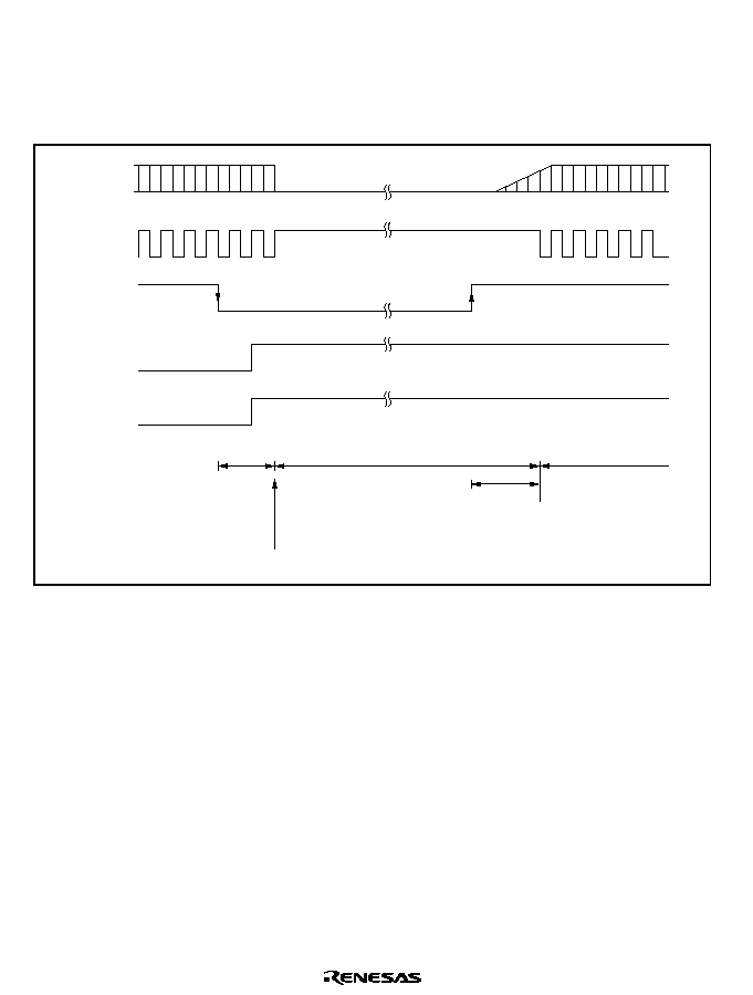
Rev. 2.0, 04/02, page 794 of 906
In this example, an NMI interrupt is accepted with the NMIEG bit in INTCR cleared to 0 (falling
edge specification), then the NMIEG bit is set to 1 (rising edge specification), the SSBY bit is set
to 1, and a SLEEP instruction is executed, causing a transition to software standby mode.
Software standby mode is then cleared at the rising edge on the NMI pin.
Oscillator
¯
NMI
NMIEG
SSBY
NMI exception
handling
NMIEG=1
SSBY=1
SLEEP instruction
Software standby mode
(power-down mode)
Oscillation
stabilization
time t
OSC2
NMI exception
handling
Figure 22.2 Software Standby Mode Application Example
22.2.4
Hardware Standby Mode
Transition to Hardware Standby Mode: When the
67%< pin is driven low, a transition is made
to hardware standby mode from any mode.
In hardware standby mode, all functions enter the reset state and stop operation, resulting in a
significant reduction in power dissipation. As long as the prescribed voltage is supplied, on-chip
RAM data is retained. I/O ports are set to the high-impedance state.
In order to retain on-chip RAM data, the RAME bit in SYSCR should be cleared to 0 before
driving the
67%< pin low. Do not change the state of the mode pins (MD2 to MD0) while this
LSI is in hardware standby mode.
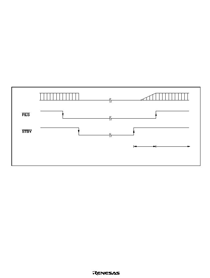
Rev. 2.0, 04/02, page 795 of 906
Clearing Hardware Standby Mode: Hardware standby mode is cleared by means of the
67%<
pin and the
5(6 pin. When the 67%< pin is driven high while the 5(6 pin is low, the reset state is
set and clock oscillation is started. Ensure that the
5(6 pin is held low until the clock oscillator
stabilizes (for details on the oscillation stabilization time, refer to table 22.2). When the
5(6 pin is
subsequently driven high, a transition is made to the program execution state via the reset
exception handling state.
Hardware Standby Mode Timing: Figure 22.3 shows an example of hardware standby mode
timing.
When the
67%< pin is driven low after the 5(6 pin has been driven low, a transition is made to
hardware standby mode. Hardware standby mode is cleared by driving the
67%< pin high, waiting
for the oscillation stabilization time, then changing the
5(6 pin from low to high.
Oscillator
Oscillation
stabilization
time
Reset
exception
handling
Figure 22.3 Hardware Standby Mode Timing
22.2.5
Module Stop Mode
Module stop mode can be set for individual on-chip peripheral modules.
When the corresponding MSTP bit in MSTPCR is set to 1, module operation stops at the end of
the bus cycle and a transition is made to module stop mode. The CPU continues operating
independently.
When the corresponding MSTP bit is cleared to 0, module stop mode is cleared and the module
starts operating at the end of the bus cycle. In module stop mode, the internal states of modules
other than the SCI are retained.
After reset clearance, all modules other than the EXDMAC, DMAC, and DTC are in module stop
mode.

Rev. 2.0, 04/02, page 796 of 906
The module registers which are set in module stop mode cannot be read or written to.
22.2.6
All-Module-Clocks-Stop Mode
When the ACSE bit in MSTPCRH is set to 1 and module stop mode is set for all the on-chip
peripheral functions controlled by MSTPCR (MSTPCR = H'FFFF), or for all the on-chip
peripheral functions except the 8-bit timer (MSTPCR = H'FFFE), executing a SLEEP instruction
while the SSBY bit in SBYCR is cleared to 0 will cause all the on-chip peripheral functions
(except the 8-bit timer and watchdog timer), the bus controller, and the I/O ports to stop operating,
and a transition to be made to all-module-clocks-stop mode, at the end of the bus cycle.
Operation or halting of the 8-bit timer can be selected by means of the MSTP0 bit.
All-module-clocks-stop mode is cleared by an external interrupt (NMI,
,54 to ,54 pins), 5(6
pin input, or an internal interrupt (8-bit timer, watchdog timer), and the CPU returns to the normal
program execution state via the exception handling state. All-module-clocks-stop mode is not
cleared if interrupts are disabled, if interrupts other than NMI are masked by the CPU, or if the
relevant interrupt is designated as a DTC activation source.
When the
67%< pin is driven low, a transition is made to hardware standby mode.
22.3
¯ Clock Output Control
Output of the ¯ clock can be controlled by means of the PSTOP bit in SCKCR, and DDR for the
corresponding port. When the PSTOP bit is set to 1, the ¯ clock stops at the end of the bus cycle,
and ¯ output goes high. ¯ clock output is enabled when the PSTOP bit is cleared to 0. When DDR
for the corresponding port is cleared to 0, ¯ clock output is disabled and input port mode is set.
Table 22.3 shows the state of the ¯ pin in each processing state.
Table 22.3 ¯ Pin State in Each Processing State
Register Setting
DDR
PSTOP
Normal
operating state
Sleep mode
Software
standby mode
Hardware
standby mode
All-module-
clocks-stop
mode
0
X
High impedance
High impedance
High impedance
High impedance
High impedance
1
0
¯ output
¯ output
Fixed high
High impedance
¯ output
1
1
Fixed high
Fixed high
Fixed high
High impedance
Fixed high

Rev. 2.0, 04/02, page 797 of 906
22.4
Usage Notes
22.4.1
I/O Port Status
In software standby mode, I/O port states are retained. Therefore, there is no reduction in current
dissipation for the output current when a high-level signal is output.
22.4.2
Current Dissipation during Oscillation Stabilization Standby Period
Current dissipation increases during the oscillation stabilization standby period.
22.4.3
EXDMAC/DMAC/DTC Module Stop
Depending on the operating status of the EXDMAC, DMAC, or DTC, the MSTP14 to MSTP12
bits may not be set to 1. Setting of the EXDMAC, DMAC, or DTC module stop mode should be
carried out only when the respective module is not activated.
For details, refer to section 8, EXDMA Controller (EXDMAC), section 7, DMA Controller
(DMAC), and section 9, Data Transfer Controller (DTC).
22.4.4
On-Chip Peripheral Module Interrupts
Relevant interrupt operations cannot be performed in module stop mode. Consequently, if module
stop mode is entered when an interrupt has been requested, it will not be possible to clear the CPU
interrupt source or the EXDMAC, DMAC, or DTC activation source.
Interrupts should therefore be disabled before entering module stop mode.
22.4.5
Writing to MSTPCR
MSTPCR should only be written to by the CPU.

Rev. 2.0, 04/02, page 798 of 906

Rev. 2.0, 04/02, page 799 of 906
Section 23 List of Registers
This section gives information on the on-chip I/O registers and is configured as described below.
1. Register Addresses (by functional module, in order of the corresponding section numbers)
∑
Descriptions by functional module, in order of the corresponding section numbers
Entries that consist of
lines are for separation of the functional modules.
∑
Access to reserved addresses which are not described in this list is prohibited.
∑
When registers consist of 16 or 32 bits, the addresses of the MSBs are given, on the
presumption of a big-endian system.
2. Register Bits
∑
Bit configurations of the registers are described in the same order as the Register Addresses
(by functional module, in order of the corresponding section numbers).
∑
Reserved bits are indicated by
in the bit name.
∑
No entry in the bit-name column indicates that the whole register is allocated as a counter or
for holding data.
∑
When registers consist of 16 or 32 bits, bits are described from the MSB side.
The order in which bytes are described is on the presumption of a big-endian system.
3. Register States in Each Operating Mode
∑
Register states are described in the same order as the Register Addresses (by functional
module, in order of the corresponding section numbers).
∑
For the initial state of each bit, refer to the description of the register in the corresponding
section.
∑
The register states described are for the basic operating modes. If there is a specific reset for an
on-chip module, refer to the section on that on-chip module.

Rev. 2.0, 04/02, page 800 of 906
23.1
Register Addresses
(by functional module, in order of the corresponding section
numbers)
Entries under Access size indicates numbers of bits.
Note:
Access to undefined or reserved addresses is prohibited. Since operation or continued
operation is not guaranteed when these registers are accessed, do not attempt such access.

Rev. 2.0, 04/02, page 801 of 906
Register Name
Abbrevia-
tion
Bit No.
Address
Module
Data
Width
Access
States
DTC mode register A
MRA
8
H'BC00 to DTC
16/32
2
DTC source address register
SAR
24
H'BFFF
DTC
16/32
2
DTC mode register B
MRB
8
DTC
16/32
2
DTC destination address register
DAR
24
DTC
16/32
2
DTC transfer count register A
CRA
16
DTC
16/32
2
DTC transfer count register B
CRB
18
DTC
16/32
2
Serial expansion mode register
*
1
SEMR
8
H'FDA8
SCI_2
8
2
EXDMA source address register_0
EDSAR_0
32
H'FDC0
EXDMAC_0 16
2
EXDMA destination address register_0
EDDAR_0
32
H'FDC4
EXDMAC_0 16
2
EXDMA transfer count register_0
EDTCR_0
32
H'FDC8
EXDMAC_0 16
2
EXDMA mode control register_0
EDMDR_0
16
H'FDCC
EXDMAC_0 16
2
EXDMA address control register_0
EDACR_0
16
H'FDCE
EXDMAC_0 16
2
EXDMA source address register_1
EDSAR_1
32
H'FDD0
EXDMAC_1 16
2
EXDMA destination address register_1
EDDAR_1
32
H'FDD4
EXDMAC_1 16
2
EXDMA transfer count register_1
EDTCR_1
32
H'FDD8
EXDMAC_1 16
2
EXDMA mode control register_1
EDMDR_1
16
H'FDDC
EXDMAC_1 16
2
EXDMA address control register_1
EDACR_1
16
H'FDDE
EXDMAC_1 16
2
EXDMA source address register_2
EDSAR_2
32
H'FDE0
EXDMAC_2 16
2
EXDMA destination address register_2
EDDAR_2
32
H'FDE4
EXDMAC_2 16
2
EXDMA transfer count register_2
EDTCR_2
32
H'FDE8
EXDMAC_2 16
2
EXDMA mode control register_2
EDMDR_2
16
H'FDEC
EXDMAC_2 16
2
EXDMA address control register_2
EDACR_2
16
H'FDEE
EXDMAC_2 16
2
EXDMA source address register_3
EDSAR_3
32
H'FDF0
EXDMAC_3 16
2
EXDMA destination address register_3
EDDAR_3
32
H'FDF4
EXDMAC_3 16
2
EXDMA transfer count register 3
EDTCR_3
32
H'FDF8
EXDMAC_3 16
2
EXDMA mode control register 3
EDMDR_3
16
H'FDFC
EXDMAC_3 16
2
EXDMA address control register 3
EDACR_3
16
H'FDFE
EXDMAC_3 16
2
Interrupt priority register A
IPRA
16
H'FE00
INT
16
2
Interrupt priority register B
IPRB
16
H'FE02
INT
16
2
Interrupt priority register C
IPRC
16
H'FE04
INT
16
2
Interrupt priority register D
IPRD
16
H'FE06
INT
16
2
Interrupt priority register E
IPRE
16
H'FE08
INT
16
2
Interrupt priority register F
IPRF
16
H'FE0A
INT
16
2

Rev. 2.0, 04/02, page 802 of 906
Register Name
Abbrevia-
tion
Bit No.
Address
Module
Data
Width
Access
States
Interrupt priority register G
IPRG
16
H'FE0C
INT
16
2
Interrupt priority register H
IPRH
16
H'FE0E
INT
16
2
Interrupt priority register I
IPRI
16
H'FE10
INT
16
2
Interrupt priority register J
IPRJ
16
H'FE12
INT
16
2
Interrupt priority register K
IPRK
16
H'FE14
INT
16
2
IRQ pin select register
ITSR
16
H'FE16
INT
16
2
Software standby release IRQ enable
register
SSIER
16
H'FE18
INT
16
2
IRQ sense control register H
ISCRH
16
H'FE1A
INT
16
2
IRQ sense control register L
ISCRL
16
H'FE1C
INT
16
2
IrDA control register_0
IrCR_0
8
H'FE1E
IrDA_0
8
2
Port 1 data direction register
P1DDR
8
H'FE20
PORT
8
2
Port 2 data direction register
P2DDR
8
H'FE21
PORT
8
2
Port 3 data direction register
P3DDR
8
H'FE22
PORT
8
2
Port 5 data direction register
P5DDR
8
H'FE24
PORT
8
2
Port 6 data direction register
P6DDR
8
H'FE25
PORT
8
2
Port 7 data direction register
P7DDR
8
H'FE26
PORT
8
2
Port 8 data direction register
P8DDR
8
H'FE27
PORT
8
2
Port A data direction register
PADDR
8
H'FE29
PORT
8
2
Port B data direction register
PBDDR
8
H'FE2A
PORT
8
2
Port C data direction register
PCDDR
8
H'FE2B
PORT
8
2
Port D data direction register
PDDDR
8
H'FE2C
PORT
8
2
Port E data direction register
PEDDR
8
H'FE2D
PORT
8
2
Port F data direction register
PFDDR
8
H'FE2E
PORT
8
2
Port G data direction register
PGDDR
8
H'FE2F
PORT
8
2
Port function control register 0
PFCR0
8
H'FE32
PORT
8
2
Port function control register 1
PFCR1
8
H'FE33
PORT
8
2
Port function control register 2
PFCR2
8
H'FE34
PORT
8
2
Port A pull-up MOS control register
PAPCR
8
H'FE36
PORT
8
2
Port B pull-up MOS control register
PBPCR
8
H'FE37
PORT
8
2
Port C pull-up MOS control register
PCPCR
8
H'FE38
PORT
8
2
Port D pull-up MOS control register
PDPCR
8
H'FE39
PORT
8
2

Rev. 2.0, 04/02, page 803 of 906
Register Name
Abbrevia-
tion
Bit No.
Address
Module
Data
Width
Access
States
Port E pull-up MOS control register
PEPCR
8
H'FE3A
PORT
8
2
Port 3 open drain control register
P3ODR
8
H'FE3C
PORT
8
2
Port A open drain control register
PAODR
8
H'FE3D
PORT
8
2
Timer control register_3
TCR_3
8
H'FE80
TPU_3
16
2
Timer mode register_3
TMDR_3
8
H'FE81
TPU_3
16
2
Timer I/O control register H_3
TIORH_3
8
H'FE82
TPU_3
16
2
Timer I/O control register L_3
TIORL_3
8
H'FE83
TPU_3
16
2
Timer interrupt enable register_3
TIER_3
8
H'FE84
TPU_3
16
2
Timer status register_3
TSR_3
8
H'FE85
TPU_3
16
2
Timer counter_3
TCNT_3
16
H'FE86
TPU_3
16
2
Timer general register A_3
TGRA_3
16
H'FE88
TPU_3
16
2
Timer general register B_3
TGRB_3
16
H'FE8A
TPU_3
16
2
Timer general register C_3
TGRC_3
16
H'FE8C
TPU_3
16
2
Timer general register D_3
TGRD_3
16
H'FE8E
TPU_3
16
2
Timer control register_4
TCR_4
8
H'FE90
TPU_4
16
2
Timer mode register_4
TMDR_4
8
H'FE91
TPU_4
16
2
Timer I/O control register_4
TIOR_4
8
H'FE92
TPU_4
16
2
Timer interrupt enable register_4
TIER_4
8
H'FE94
TPU_4
16
2
Timer status register_4
TSR_4
8
H'FE95
TPU_4
16
2
Timer counter_4
TCNT_4
16
H'FE96
TPU_4
16
2
Timer general register A_4
TGRA_4
16
H'FE98
TPU_4
16
2
Timer general register B_4
TGRB_4
16
H'FE9A
TPU_4
16
2
Timer control register_5
TCR_5
8
H'FEA0
TPU_5
16
2
Timer mode register_5
TMDR_5
8
H'FEA1
TPU_5
16
2
Timer I/O control register_5
TIOR_5
8
H'FEA2
TPU_5
16
2
Timer interrupt enable register_5
TIER_5
8
H'FEA4
TPU_5
16
2
Timer status register_5
TSR_5
8
H'FEA5
TPU_5
16
2
Timer counter_5
TCNT_5
16
H'FEA6
TPU_5
16
2
Timer general register A_5
TGRA_5
16
H'FEA8
TPU_5
16
2
Timer general register B_5
TGRB_5
16
H'FEAA
TPU_5
16
2
Bus width control register
ABWCR
8
H'FEC0
BSC
16
2
Access state control register
ASTCR
8
H'FEC1
BSC
16
2
Wait control register AH
WTCRAH
8
H'FEC2
BSC
16
2

Rev. 2.0, 04/02, page 804 of 906
Register Name
Abbrevia-
tion
Bit No.
Address
Module
Data
Width
Access
States
Wait control register AL
WTCRAL
8
H'FEC3
BSC
16
2
Wait control register BH
WTCRBH
8
H'FEC4
BSC
16
2
Wait control register BL
WTCRBL
8
H'FEC5
BSC
16
2
Read strobe timing control register
RDNCR
8
H'FEC6
BSC
16
2
Chip select assertion period control
registers H
CSACRH
8
H'FEC8
BSC
16
2
Chip select assertion period control
register L
CSACRL
8
H'FEC9
BSC
16
2
Burst ROM interface control register H
BROMCRH
8
H'FECA
BSC
16
2
Burst ROM interface control register L
BROMCRL
8
H'FECB
BSC
16
2
Bus control register
BCR
16
H'FECC
BSC
16
2
RAM emulation register
*
3
RAMER
8
H'FECE
FLASH
16
2
DRAM control register L
DRAMCR
16
H'FED0
BSC
16
2
DRAM access control register
DRACCR
8/16
*
2
H'FED2
BSC
16
2
Refresh control register
REFCR
16
H'FED4
BSC
16
2
Refresh timer counter
RTCNT
8
H'FED6
BSC
16
2
Refresh time constant register
RTCOR
8
H'FED7
BSC
16
2
Memory address register 0AH
MAR0AH
16
H'FEE0
DMAC
16
2
Memory address register 0AL
MAR_0AL
16
H'FEE2
DMAC
16
2
I/O address register 0A
IOAR_0A
16
H'FEE4
DMAC
16
2
Transfer count register 0A
ETCR_0A
16
H'FEE6
DMAC
16
2
Memory address register 0BH
MAR_0BH
16
H'FEE8
DMAC
16
2
Memory address register 0BL
MAR_0BL
16
H'FEEA
DMAC
16
2
I/O address register 0B
IOAR_0B
16
H'FEEC
DMAC
16
2
Transfer count register 0B
ETCR_0B
16
H'FEEE
DMAC
16
2
Memory address register 1AH
MAR_1AH
16
H'FEF0
DMAC
16
2
Memory address register 1AL
MAR_1AL
16
H'FEF2
DMAC
16
2
I/O address register 1A
IOAR_1A
16
H'FEF4
DMAC
16
2
Transfer count register 1A
ETCR_1A
16
H'FEF6
DMAC
16
2
Memory address register 1BH
MAR_1BH
16
H'FEF8
DMAC
16
2
Memory address register 1BL
MAR_1BL
16
H'FEFA
DMAC
16
2
I/O address register 1B
IOAR_1B
16
H'FEFC
DMAC
16
2
Transfer count register 1B
ETCR_1B
16
H'FEFE
DMAC
16
2

Rev. 2.0, 04/02, page 805 of 906
Register Name
Abbrevia-
tion
Bit No.
Address
Module
Data
Width
Access
States
DMA write enable register
DMAWER
8
H'FF20
DMAC
8
2
DMA terminal control register
DMATCR
8
H'FF21
DMAC
8
2
DMA control register 0A
DMACR_0A 8
H'FF22
DMAC
16
2
DMA control register 0B
DMACR_0B 8
H'FF23
DMAC
16
2
DMA control register 1A
DMACR_1A 8
H'FF24
DMAC
16
2
DMA control register 1B
DMACR_1B 8
H'FF25
DMAC
16
2
DMA band control register H
DMABCRH
8
H'FF26
DMAC
16
2
DMA band control register L
DMABCRL
8
H'FF27
DMAC
16
2
DTC enable register A
DTCERA
8
H'FF28
DTC
16
2
DTC enable register B
DTCERB
8
H'FF29
DTC
16
2
DTC enable register C
DTCERC
8
H'FF2A
DTC
16
2
DTC enable register D
DTCERD
8
H'FF2B
DTC
16
2
DTC enable register E
DTCERE
8
H'FF2C
DTC
16
2
DTC enable register F
DTCERF
8
H'FF2D
DTC
16
2
DTC enable register G
DTCERG
8
H'FF2E
DTC
16
2
DTC vector register
DTVECR
8
H'FF30
DTC
16
2
Interrupt control register
INTCR
8
H'FF31
INT
16
2
IRQ enable register
IER
16
H'FF32
INT
16
2
IRQ status register
ISR
16
H'FF34
INT
16
2
Standby control register
SBYCR
8
H'FF3A
SYSTEM
8
2
System clock control register
SCKCR
8
H'FF3B
SYSTEM
8
2
System control register
SYSCR
8
H'FF3D
SYSTEM
8
2
Mode control register
MDCR
8
H'FF3E
SYSTEM
8
2
Module stop control register H
MSTPCRH
8
H'FF40
SYSTEM
8
2
Module stop control register L
MSTPCRL
8
H'FF41
SYSTEM
8
2
PLL control register
PLLCR
8
H'FF45
SYSTEM
8
2
PPG output control register
PCR
8
H'FF46
PPG
8
2
PPG output mode register
PMR
8
H'FF47
PPG
8
2
Next data enable register H
NDERH
8
H'FF48
PPG
8
2
Next data enable register L
NDERL
8
H'FF49
PPG
8
2
Output data register H
PODRH
8
H'FF4A
PPG
8
2
Output data register L
PODRL
8
H'FF4B
PPG
8
2
Next data register H
*
4
NDRH
8
H'FF4C
PPG
8
2

Rev. 2.0, 04/02, page 806 of 906
Register Name
Abbrevia-
tion
Bit No.
Address
Module
Data
Width
Access
States
Next data register L
*
4
NDRL
8
H'FF4D
PPG
8
2
Next data register H
*
4
NDRH
8
H'FF4E
PPG
8
2
Next data register L
*
4
NDRL
8
H'FF4F
PPG
8
2
Port 1 register
PORT1
8
H'FF50
PORT
8
2
Port 2 register
PORT2
8
H'FF51
PORT
8
2
Port 3 register
PORT3
8
H'FF52
PORT
8
2
Port 4 register
PORT4
8
H'FF53
PORT
8
2
Port 5 register
PORT5
8
H'FF54
PORT
8
2
Port 6 register
PORT6
8
H'FF55
PORT
8
2
Port 7 register
PORT7
8
H'FF56
PORT
8
2
Port 8 register
PORT8
8
H'FF57
PORT
8
2
Port A register
PORTA
8
H'FF59
PORT
8
2
Port B register
PORTB
8
H'FF5A
PORT
8
2
Port C register
PORTC
8
H'FF5B
PORT
8
2
Port D register
PORTD
8
H'FF5C
PORT
8
2
Port E register
PORTE
8
H'FF5D
PORT
8
2
Port F register
PORTF
8
H'FF5E
PORT
8
2
Port G register
PORTG
8
H'FF5F
PORT
8
2
Port 1 data register
P1DR
8
H'FF60
PORT
8
2
Port 2 data register
P2DR
8
H'FF61
PORT
8
2
Port 3 data register
P3DR
8
H'FF62
PORT
8
2
Port 5 data register
P5DR
8
H'FF64
PORT
8
2
Port 6 data register
P6DR
8
H'FF65
PORT
8
2
Port 7 data register
P7DR
8
H'FF66
PORT
8
2
Port 8 data register
P8DR
8
H'FF67
PORT
8
2
Port A data register
PADR
8
H'FF69
PORT
8
2
Port B data register
PBDR
8
H'FF6A
PORT
8
2
Port C data register
PCDR
8
H'FF6B
PORT
8
2
Port D data register
PDDR
8
H'FF6C
PORT
8
2
Port E data register
PEDR
8
H'FF6D
PORT
8
2
Port F data register
PFDR
8
H'FF6E
PORT
8
2
Port G data register
PGDR
8
H'FF6F
PORT
8
2

Rev. 2.0, 04/02, page 807 of 906
Register Name
Abbrevia-
tion
Bit No.
Address
Module
Data
Width
Access
States
Port H register
PORTH
8
H'FF70
PORT
8
2
Port H data register
PHDR
8
H'FF72
PORT
8
2
Port H data direction register
PHDDR
8
H'FF74
PORT
8
2
Serial mode register_0
SMR_0
8
H'FF78
SCI_0
8
2
Bit rate register_0
BRR_0
8
H'FF79
SCI_0
8
2
Serial control register_0
SCR_0
8
H'FF7A
SCI_0
8
2
Transmit data register_0
TDR_0
8
H'FF7B
SCI_0
8
2
Serial status register_0
SSR_0
8
H'FF7C
SCI_0
8
2
Receive data register_0
RDR_0
8
H'FF7D
SCI_0
8
2
Smart card mode register_0
SCMR_0
8
H'FF7E
SCI_0
8
2
Serial mode register_1
SMR_1
8
H'FF80
SCI_1
8
2
Bit rate register_1
BRR_1
8
H'FF81
SCI_1
8
2
Serial control register_1
SCR_1
8
H'FF82
SCI_1
8
2
Transmit data register_1
TDR_1
8
H'FF83
SCI_1
8
2
Serial status register_1
SSR_1
8
H'FF84
SCI_1
8
2
Receive data register_1
RDR_1
8
H'FF85
SCI_1
8
2
Smart card mode register_1
SCMR_1
8
H'FF86
SCI_1
8
2
Serial mode register_2
SMR_2
8
H'FF88
SCI_2
8
2
Bit rate register_2
BRR_2
8
H'FF89
SCI_2
8
2
Serial control register_2
SCR_2
8
H'FF8A
SCI_2
8
2
Transmit data register_2
TDR_2
8
H'FF8B
SCI_2
8
2
Serial status register_2
SSR_2
8
H'FF8C
SCI_2
8
2
Receive data register_2
RDR_2
8
H'FF8D
SCI_2
8
2
Smart card mode register_2
SCMR_2
8
H'FF8E
SCI_2
8
2
A/D data register A
(H8S/2678R Series)
ADDRA
16
H'FF90
A/D
16
2
A/D data register AH
(H8S/2678 Series)
ADDRAH
8
H'FF90
A/D
8
2
A/D data register AL
(H8S/2678 Series)
ADDRAL
8
H'FF91
A/D
8
2
A/D data register B
(H8S/2678R Series)
ADDRB
16
H'FF92
A/D
16
2
A/D data register BH
(H8S/2678 Series)
ADDRBH
8
H'FF92
A/D
8
2

Rev. 2.0, 04/02, page 808 of 906
Register Name
Abbrevia-
tion
Bit No.
Address
Module
Data
Width
Access
States
A/D data register BL
(H8S/2678 Series)
ADDRBL
8
H'FF93
A/D
8
2
A/D data register C
(H8S/2678R Series)
ADDRC
16
H'FF94
A/D
16
2
A/D data register CH
(H8S/2678 Series)
ADDRCH
8
H'FF94
A/D
8
2
A/D data register CL
(H8S/2678 Series)
ADDRCL
8
H'FF95
A/D
8
2
A/D data register D
(H8S/2678R Series)
ADDRD
16
H'FF96
A/D
16
2
A/D data register DH
(H8S/2678 Series)
ADDRDH
8
H'FF96
A/D
8
2
A/D data register DL
(H8S/2678 Series)
ADDRDL
8
H'FF97
A/D
8
2
A/D control/status register
(H8S/2678 Series)
ADCSR
8
H'FF98
A/D
8
2
A/D data register E
(H8S/2678R Series)
ADDRE
16
H'FF98
A/D
16
2
A/D control register
(H8S/2678 Series)
ADCR
8
H'FF99
A/D
8
2
A/D data register F
(H8S/2678R Series)
ADDRF
16
H'FF9A
A/D
16
2
A/D data register G
(H8S/2678R Series)
ADDRG
16
H'FF9C
A/D
16
2
A/D data register H
(H8S/2678R Series)
ADDRH
16
H'FF9E
A/D
16
2
A/D control/status register
(H8S/2678R Series)
ADCSR
8
H'FFA0
A/D
16
2
A/D control register
(H8S/2678R Series)
ADCR
8
H'FFA1
A/D
16
2
D/A data register 0
DADR0
8
H'FFA4
D/A
8
2
D/A data register 1
DADR1
8
H'FFA5
D/A
8
2
D/A control register 01
DACR01
8
H'FFA6
D/A
8
2
D/A data register 2
DADR2
8
H'FFA8
D/A
8
2
D/A data register 3
DADR3
8
H'FFA9
D/A
8
2
D/A control register 23
DACR23
8
H'FFAA
D/A
8
2
Timer control register 0
TCR_0
8
H'FFB0
TMR_0
16
2
Timer control register 1
TCR_1
8
H'FFB1
TMR_1
16
2

Rev. 2.0, 04/02, page 809 of 906
Register Name
Abbrevia-
tion
Bit No.
Address
Module
Data
Width
Access
States
Timer control/status register 0
TCSR_0
8
H'FFB2
TMR_0
16
2
Timer control/status register 1
TCSR_1
8
H'FFB3
TMR_1
16
2
Time constant register A0
TCORA_0
8
H'FFB4
TMR_0
16
2
Time constant register A1
TCORA_1
8
H'FFB5
TMR_1
16
2
Time constant register B0
TCORB_0
8
H'FFB6
TMR_0
16
2
Time constant register B1
TCORB_1
8
H'FFB7
TMR_1
16
2
Timer counter 0
TCNT_0
8
H'FFB8
TMR_0
16
2
Timer counter 1
TCNT_1
8
H'FFB9
TMR_1
16
2
Timer control/status register
TCSR
8
H'FFBC
*
4
(Write)
WDT
16
2
H'FFBC
(Read)
Timer counter
TCNT
8
H'FFBC
*
4
(Write)
WDT
16
2
H'FFBD
(Read)
Reset control/status register
RSTCSR
8
H'FFBE
*
4
(Write)
WDT
16
2
H'FFBF
(Read)
Timer start register
TSTR
8
H'FFC0
TPU
16
2
Timer synchronous register
TSYR
8
H'FFC1
TPU
16
2
Flash memory control register 1
*
3
FLMCR1
8
H'FFC8
FLASH
8
2
Flash memory control register 2
*
3
FLMCR2
8
H'FFC9
FLASH
8
2
Erase block register 1
*
3
EBR1
8
H'FFCA
FLASH
8
2
Erase block register 2
*
3
EBR2
8
H'FFCB
FLASH
8
2
Timer control register_0
TCR_0
8
H'FFD0
TPU_0
16
2
Timer mode register_0
TMDR_0
8
H'FFD1
TPU_0
16
2
Timer I/O control register H_0
TIORH_0
8
H'FFD2
TPU_0
16
2
Timer I/O control register L_0
TIORL_0
8
H'FFD3
TPU_0
16
2
Timer interrupt enable register_0
TIER_0
8
H'FFD4
TPU_0
16
2
Timer status register_0
TSR_0
8
H'FFD5
TPU_0
16
2
Timer counter_0
TCNT_0
16
H'FFD6
TPU_0
16
2
Timer general register A_0
TGRA_0
16
H'FFD8
TPU_0
16
2
Timer general register B_0
TGRB_0
16
H'FFDA
TPU_0
16
2

Rev. 2.0, 04/02, page 810 of 906
Register Name
Abbrevia-
tion
Bit No.
Address
Module
Data
Width
Access
States
Timer general register C_0
TGRC_0
16
H'FFDC
TPU_0
16
2
Timer general register D_0
TGRD_0
16
H'FFDE
TPU_0
16
2
Timer control register_1
TCR_1
8
H'FFE0
TPU_1
16
2
Timer mode register_1
TMDR_1
8
H'FFE1
TPU_1
16
2
Timer I/O control register_1
TIOR_1
8
H'FFE2
TPU_1
16
2
Timer interrupt enable register_1
TIER_1
8
H'FFE4
TPU_1
16
2
Timer status register_1
TSR_1
8
H'FFE5
TPU_1
16
2
Timer counter_1
TCNT_1
16
H'FFE6
TPU_1
16
2
Timer general register A_1
TGRA_1
16
H'FFE8
TPU_1
16
2
Timer general register B_1
TGRB_1
16
H'FFEA
TPU_1
16
2
Timer control register_2
TCR_2
8
H'FFF0
TPU_2
16
2
Timer mode register_2
TMDR_2
8
H'FFF1
TPU_2
16
2
Timer I/O control register_2
TIOR_2
8
H'FFF2
TPU_2
16
2
Timer interrupt enable register_2
TIER_2
8
H'FFF4
TPU_2
16
2
Timer status rgister_2
TSR_2
8
H'FFF5
TPU_2
16
2
Timer counter_2
TCNT_2
16
H'FFF6
TPU_2
16
2
Timer general register A_2
TGRA_2
16
H'FFF8
TPU_2
16
2
Timer general register B_2
TGRB_2
16
H'FFFA
TPU_2
16
2
Notes: 1.
Not available in the H8S/2678 Series.
2. In the H8S/2678 Series: 8 bits, in the H8S/2678R Series: 16 bits.
3. Register of the flash memory version. Not available in the masked ROM version and
ROM-less version.
4. If the pulse output group 2 and pulse output group 3 output triggers are the same
according to the PCR setting, the NDRH address will be H'FF4C, and if different, the
address of NDRH for group 2 will be H'FF4E, and that for group 3 will be H'FF4C.
Similarly, if the pulse output group 0 and pulse output group 1 output triggers are the
same according to the PCR setting, the NDRL address will be H'FF4D, and if different,
the address of NDRL for group 0 will be H'FF4F, and that for group 1 will be H'FF4D.
5. For writing, refer to section 14.6.1, Notes on register access.

Rev. 2.0, 04/02, page 811 of 906
23.2
Register Bits
Register addresses and bit names of the on-chip peripheral modules are described below.
Each line covers eight bits, and 16-bit and 32-bit registers are shown as 2 or 4 lines, respectively.
Register
Abbreviation
Bit 7
Bit 6
Bit 5
Bit 4
Bit 3
Bit 2
Bit 1
Bit 0
Module
MRA
AM1
SM0
DM1
DM0
MD1
MD0
DTS
Sz
DTC
*
9
SAR
--
--
--
--
--
--
--
--
--
--
--
--
--
--
--
--
--
--
--
--
--
--
--
--
MRB
CHNE
DISEL
CHNS
--
--
--
--
--
DAR
--
--
--
--
--
--
--
--
--
--
--
--
--
--
--
--
--
--
--
--
--
--
--
--
CRA
--
--
--
--
--
--
--
--
--
--
--
--
--
--
--
--
--
--
--
--
--
--
--
--
CRB
--
--
--
--
--
--
--
--
--
--
--
--
--
--
--
--
--
--
--
--
--
--
--
--
SEMR
*
8
--
--
--
--
ABCS
ACS2
ACS1
ACS0
SCI_2
Smart card
interface 2
EDSAR_0
--
--
--
--
--
--
--
--
EXDMAC_0
EDDAR_0
--
--
--
--
--
--
--
--
EDTCR_0
--
--
--
--
--
--
--
--
EDA
BEF
EDRAKE
ETENDE
EDREQS
AMS
MDS1
MDS0
EDMDR_0
EDIE
IRF
TCEIE
SDIR
DTSIZE
BGUP
--
--
SAT1
SAT0
SARIE
SARA4
SARA3
SARA2
SARA1
SARA0
EDACR_0
DAT1
DAT0
DARIE
DARA4
DARA3
DARA2
DARA1
DARA0
EDSAR_1
--
--
--
--
--
--
--
--
EDDAR_1
--
--
--
--
--
--
--
--
EDTCR_1
--
--
--
--
--
--
--
--
EDA
BEF
EDRAKE
ETENDE
EDREQS
AMS
MDS1
MDS0
EDMDR_1
EDIE
IRF
TCEIE
SDIR
DTSIZE
BGUP
--
--
SAT1
SAT0
SARIE
SARA4
SARA3
SARA2
SARA1
SARA0
EDACR_1
DAT1
DAT0
DARIE
DARA4
DARA3
DARA2
DARA1
DARA0
EXDMAC_1

Rev. 2.0, 04/02, page 812 of 906
Register
Abbreviation
Bit 7
Bit 6
Bit 5
Bit 4
Bit 3
Bit 2
Bit 1
Bit 0
Module
EDSAR_2
--
--
--
--
--
--
--
--
EDDAR_2
--
--
--
--
--
--
--
--
EDTCR_2
--
--
--
--
--
--
--
--
EDA
BEF
EDRAKE
ETENDE
EDREQS
AMS
MDS1
MDS0
EDMDR_2
EDIE
IRF
TCEIE
SDIR
DTSIZE
BGUP
--
--
SAT1
SAT0
SARIE
SARA4
SARA3
SARA2
SARA1
SARA0
EDACR_2
DAT1
DAT0
DARIE
DARA4
DARA3
DARA2
DARA1
DARA0
EXDMAC_2
EDSAR_3
--
--
--
--
--
--
--
--
EDDAR_3
--
--
--
--
--
--
--
--
EDTCR_3
--
--
--
--
--
--
--
--
EDA
BEF
EDRAKE
ETENDE
EDREQS
AMS
MDS1
MDS0
EDMDR_3
EDIE
IRF
TCEIE
SDIR
DTSIZE
BGUP
--
--
SAT1
SAT0
SARIE
SARA4
SARA3
SARA2
SARA1
SARA0
EDACR_3
DAT1
DAT0
DARIE
DARA4
DARA3
DARA2
DARA1
DARA0
EXDMAC_3

Rev. 2.0, 04/02, page 813 of 906
Register
Abbreviation
Bit 7
Bit 6
Bit 5
Bit 4
Bit 3
Bit 2
Bit 1
Bit 0
Module
--
IPRA14
IPRA13
IPRA12
--
IPRA10
IPRA9
IPRA8
IPRA
--
IPRA6
IPRA5
IPRA4
--
IPRA2
IPRA1
IPRA0
--
IPRB14
IPRB13
IPRB12
--
IPRB10
IPRB9
IPRB8
IPRB
--
IPRB6
IPRB5
IPRB4
--
IPRB2
IPRB1
IPRB0
--
IPRC14
IPRC13
IPRC12
--
IPRC10
IPRC9
IPRC8
IPRC
--
IPRC6
IPRC5
IPRC4
--
IPRC2
IPRC1
IPRC0
--
IPRD14
IPRD13
IPRD12
--
IPRD10
IPRD9
IPRD8
IPRD
--
IPRD6
IPRD5
IPRD4
--
IPRD2
IPRD1
IPRD0
--
IPRE14
IPRE13
IPRE12
--
IPRE10
IPRE9
IPRE8
IPRE
--
IPRE6
IPRE5
IPRE4
--
IPRE2
IPRE1
IPRE0
--
IPRF14
IPRF13
IPRF12
--
IPRF10
IPRF9
IPRF8
IPRF
--
IPRF6
IPRF5
IPRF4
--
IPRF2
IPRF1
IPRF0
--
IPRG14
IPRG13
IPRG12
--
IPRG10
IPRG9
IPRG8
IPRG
--
IPRG6
IPRG5
IPRG4
--
IPRG2
IPRG1
IPRG0
--
IPRH14
IPRH13
IPRH12
--
IPRH10
IPRH9
IPRH8
IPRH
--
IPRH6
IPRH5
IPRH4
--
IPRH2
IPRH1
IPRH0
--
IPRI14
IPRI13
IPRI12
--
IPRI10
IPRI9
IPRI8
IPRI
--
IPRI6
IPRI5
IPRI4
--
IPRI2
IPRI1
IPRI0
--
IPRJ14
IPRJ13
IPRJ12
--
IPRJ10
IPRJ9
IPRJ8
IPRJ
--
IPRJ6
IPRJ5
IPRJ4
--
IPRJ2
IPRJ1
IPRJ0
--
IPRK14
IPRK13
IPRK12
--
IPRK10
IPRK9
IPRK8
IPRK
--
IPRK6
IPRK5
IPRK4
--
IPRK2
IPRK1
IPRK0
ITS15
ITS14
ITS13
ITS12
ITS11
ITS10
ITS9
ITS8
ITSR
ITS7
ITS6
ITS5
ITS4
ITS3
ITS2
ITS1
ITS0
SSI15
SSI14
SSI13
SSI12
SSI11
SSI10
SSI9
SSI8
SSIER
SSI7
SSI6
SSI5
SSI4
SSI3
SSI2
SSI1
SSI0
IRQ15SCB IRQ15SCA IRQ14SCB IRQ14SCA IRQ13SCB IRQ13SCA IRQ12SCB IRQ12SCA
ISCRH
IRQ11SCB IRQ11SCA IRQ10SCB IRQ10SCA IRQ9SCB
IRQ9SCA
IRQ8SCB
IRQ8SCA
IRQ7SCB
IRQ7SCA
IRQ6SCB
IRQ6SCA
IRQ5SCB
IRQ5SCA
IRQ4SCB
IRQ4SCA
ISCRL
IRQ3SCB
IRQ3SCA
IRQ2SCB
IRQ2SCA
IRQ1SCB
IRQ1SCA
IRQ0SCB
IRQ0SCA
INT
IrCR_0
IrE
IrCKS2
IrCKS1
IrCKS0
--
--
--
--
IrDA_0

Rev. 2.0, 04/02, page 814 of 906
Register
Abbreviation
Bit 7
Bit 6
Bit 5
Bit 4
Bit 3
Bit 2
Bit 1
Bit 0
Module
P1DDR
P17DDR
P16DDR
P15DDR
P14DDR
P13DDR
P12DDR
P11DDR
P10DDR
P2DDR
P27DDR
P26DDR
P25DDR
P24DDR
P23DDR
P22DDR
P21DDR
P20DDR
P3DDR
--
--
P35DDR
P34DDR
P33DDR
P32DDR
P31DDR
P30DDR
P5DDR
--
--
--
--
P53DDR
P52DDR
P51DDR
P50DDR
P6DDR
--
--
P65DDR
P64DDR
P63DDR
P62DDR
P61DDR
P60DDR
P7DDR
--
--
P75DDR
P74DDR
P73DDR
P72DDR
P71DDR
P70DDR
P8DDR
--
--
P85DDR
P84DDR
P83DDR
P82DDR
P81DDR
P80DDR
PADDR
PA7DDR
PA6DDR
PA5DDR
PA4DDR
PA3DDR
PA2DDR
PA1DDR
PA0DDR
PBDDR
PB7DDR
PB6DDR
PB5DDR
PB4DDR
PB3DDR
PB2DDR
PB1DDR
PB0DDR
PCDDR
PC7DDR
PC6DDR
PC5DDR
PC4DDR
PC3DDR
PC2DDR
PC1DDR
PC0DDR
PDDDR
PD7DDR
PD6DDR
PD5DDR
PD4DDR
PD3DDR
PD2DDR
PD1DDR
PD0DDR
PEDDR
PE7DDR
PE6DDR
PE5DDR
PE4DDR
PE3DDR
PE2DDR
PE1DDR
PE0DDR
PFDDR
PF7DDR
PF6DDR
PF5DDR
PF4DDR
PF3DDR
PF2DDR
PF1DDR
PF0DDR
PGDDR
--
PG6DDR
PG5DDR
PG4DDR
PG3DDR
PG2DDR
PG1DDR
PG0DDR
PFCR0
CS7E
CS6E
CS5E
CS4E
CS3E
CS2E
CS1E
CS0E
PFCR1
A23E
A22E
A21E
A20E
A19E
A18E
A17E
A16E
PFCR2
--
--
--
--
ASOE
LWROE
OES
DMACS
PAPCR
PA7PCR
PA6PCR
PA5PCR
PA4PCR
PA3PCR
PA2PCR
PA1PCR
PA0PCR
PBPCR
PB7PCR
PB6PCR
PB5PCR
PB4PCR
PB3PCR
PB2PCR
PB1PCR
PB0PCR
PCPCR
PC7PCR
PC6PCR
PC5PCR
PC4PCR
PC3PCR
PC2PCR
PC1PCR
PC0PCR
PDPCR
PD7PCR
PD6PCR
PD5PCR
PD4PCR
PD3PCR
PD2PCR
PD1PCR
PD0PCR
PEPCR
PE7PCR
PE6PCR
PE5PCR
PE4PCR
PE3PCR
PE2PCR
PE1PCR
PE0PCR
P3ODR
--
--
P35ODR
P34ODR
P33ODR
P32ODR
P31ODR
P30ODR
PAODR
PA7ODR
PA6ODR
PA5ODR
PA4ODR
PA3ODR
PA2ODR
PA1ODR
PA0ODR
PORT
TCR_3
CCLR2
CCLR1
CCLR0
CKEG1
CKEG0
TPSC2
TPSC1
TPSC0
TMDR_3
--
--
BFB
BFA
MD3
MD2
MD1
MD0
TIORH_3
IOB3
IOB2
IOB1
IOB0
IOA3
IOA2
IOA1
IOA0
TIORL_3
IOD3
IOD2
IOD1
IOD0
IOC3
IOC2
IOC1
IOC0
TIER_3
TTGE
--
--
TCIEV
TGIED
TGIEC
TGIEB
TGIEA
TSR_3
--
--
--
TCFV
TGFD
TGFC
TGFB
TGFA
Bit15
Bit14
Bit13
Bit12
Bit11
Bit10
Bit9
Bit8
TCNT_3
Bit7
Bit6
Bit5
Bit4
Bit3
Bit2
Bit1
Bit0
TPU_3

Rev. 2.0, 04/02, page 815 of 906
Register
Abbreviation Bit 7
Bit 6
Bit 5
Bit 4
Bit 3
Bit 2
Bit 1
Bit 0
Module
Bit15
Bit14
Bit13
Bit12
Bit11
Bit10
Bit9
Bit8
TGRA_3
Bit7
Bit6
Bit5
Bit4
Bit3
Bit2
Bit1
Bit0
Bit15
Bit14
Bit13
Bit12
Bit11
Bit10
Bit9
Bit8
TGRB_3
Bit7
Bit6
Bit5
Bit4
Bit3
Bit2
Bit1
Bit0
Bit15
Bit14
Bit13
Bit12
Bit11
Bit10
Bit9
Bit8
TGRC_3
Bit7
Bit6
Bit5
Bit4
Bit3
Bit2
Bit1
Bit0
Bit15
Bit14
Bit13
Bit12
Bit11
Bit10
Bit9
Bit8
TGRD_3
Bit7
Bit6
Bit5
Bit4
Bit3
Bit2
Bit1
Bit0
TPU_3
TCR_4
--
CCLR1
CCLR0
CKEG1
CKEG0
TPSC2
TPSC1
TPSC0
TMDR_4
--
--
--
--
MD3
MD2
MD1
MD0
TIOR_4
IOB3
IOB2
IOB1
IOB0
IOA3
IOA2
IOA1
IOA0
TIER_4
TTGE
--
TCIEU
TCIEV
--
--
TGIEB
TGIEA
TSR_4
TCFD
--
TCFU
TCFV
--
--
TGFB
TGFA
Bit15
Bit14
Bit13
Bit12
Bit11
Bit10
Bit9
Bit8
TCNT_4
Bit7
Bit6
Bit5
Bit4
Bit3
Bit2
Bit1
Bit0
Bit15
Bit14
Bit13
Bit12
Bit11
Bit10
Bit9
Bit8
TGRA_4
Bit7
Bit6
Bit5
Bit4
Bit3
Bit2
Bit1
Bit0
Bit15
Bit14
Bit13
Bit12
Bit11
Bit10
Bit9
Bit8
TGRB_4
Bit7
Bit6
Bit5
Bit4
Bit3
Bit2
Bit1
Bit0
TPU_4
TCR_5
--
CCLR1
CCLR0
CKEG1
CKEG0
TPSC2
TPSC1
TPSC0
TMDR_5
--
--
--
--
MD3
MD2
MD1
MD0
TIOR_5
IOB3
IOB2
IOB1
IOB0
IOA3
IOA2
IOA1
IOA0
TIER_5
TTGE
--
TCIEU
TCIEV
--
--
TGIEB
TGIEA
TSR_5
TCFD
--
TCFU
TCFV
--
--
TGFB
TGFA
Bit15
Bit14
Bit13
Bit12
Bit11
Bit10
Bit9
Bit8
TCNT_5
Bit7
Bit6
Bit5
Bit4
Bit3
Bit2
Bit1
Bit0
Bit15
Bit14
Bit13
Bit12
Bit11
Bit10
Bit9
Bit8
TGRA_5
Bit7
Bit6
Bit5
Bit4
Bit3
Bit2
Bit1
Bit0
Bit15
Bit14
Bit13
Bit12
Bit11
Bit10
Bit9
Bit8
TGRB_5
Bit7
Bit6
Bit5
Bit4
Bit3
Bit2
Bit1
Bit0
TPU_5
ABWCR
ABW7
ABW6
ABW5
ABW4
ABW3
ABW2
ABW1
ABW0
ASTCR
AST7
AST6
AST5
AST4
AST3
AST2
AST1
AST0
WTCRAH
--
W72
W71
W70
--
W62
W61
W60
BSC

Rev. 2.0, 04/02, page 816 of 906
Register
Abbreviation
Bit 7
Bit 6
Bit 5
Bit 4
Bit 3
Bit 2
Bit 1
Bit 0
Module
WTCRAL
--
W52
W51
W50
--
W42
W41
W40
WTCRBH
--
W32
W31
W30
--
W22
W21
W20
WTCRBL
--
W12
W11
W10
--
W02
W01
W00
RDNCR
RDN7
RDN6
RDN5
RDN4
RDN3
RDN2
RDN1
RDN0
CSACRH
CSXH7
CSXH6
CSXH5
CSXH4
CSXH3
CSXH2
CSXH1
CSXH0
CSACRL
CSXT7
CSXT6
CSXT5
CSXT4
CSXT3
CSXT2
CSXT1
CSXT0
BROMCRH
BSRM0
BSTS02
BSTS01
BSTS00
--
--
BSWD01
BSWD00
BROMCRL
BSRM1
BSTS12
BSTS11
BSTS10
--
--
BSWD11
BSWD10
BRLE
BREQ0E
--
IDLC
ICIS1
ICIS0
WDBE
WAITE
BCR
--
--
--
--
--
ICIS2
*
8
--
--
BSC
RAMER
*
7
--
--
--
--
RAMS
RAM2
RAM1
RAM0
FLASH
0EE
RAST
--
CAST
--
RMTS2
RMTS1
RMTS0
DRAMCR
BE
RCDM
DDS
EDDS
--
MXC2
MXC1
MXC0
DRACCR
*
1
DRMI
--
TPC1
TPC0
SDWCD
*
8
--
RCD1
RCD0
--
--
--
--
CKSPE
*
8
--
RDXC1
*
8
RDXC0
*
8
CMF
CMIE
RCW1
RCW0
--
RTCK2
RTCK1
RTCK0
REFCR
RFSHE
CBRM
RLW1
RLW0
SLFRF
TPCS2
TPCS1
TPCS0
RTCNT
Bit7
Bit6
Bit5
Bit4
Bit3
Bit2
Bit1
Bit0
RTCOR
Bit7
Bit6
Bit5
Bit4
Bit3
Bit2
Bit1
Bit0
BSC
--
--
--
--
--
--
--
--
MAR_0AH
Bit7
Bit6
Bit5
Bit4
Bit3
Bit2
Bit1
Bit0
Bit15
Bit14
Bit13
Bit12
Bit11
Bit10
Bit9
Bit8
MAR_0AL
Bit7
Bit6
Bit5
Bit4
Bit3
Bit2
Bit1
Bit0
Bit15
Bit14
Bit13
Bit12
Bit11
Bit10
Bit9
Bit8
IOAR_0A
Bit7
Bit6
Bit5
Bit4
Bit3
Bit2
Bit1
Bit0
Bit15
Bit14
Bit13
Bit12
Bit11
Bit10
Bit9
Bit8
ETCR_0A
Bit7
Bit6
Bit5
Bit4
Bit3
Bit2
Bit1
Bit0
--
--
--
--
--
--
--
--
MAR_0BH
Bit7
Bit6
Bit5
Bit4
Bit3
Bit2
Bit1
Bit0
Bit15
Bit14
Bit13
Bit12
Bit11
Bit10
Bit9
Bit8
MAR_0BL
Bit7
Bit6
Bit5
Bit4
Bit3
Bit2
Bit1
Bit0
Bit15
Bit14
Bit13
Bit12
Bit11
Bit10
Bit9
Bit8
IOAR_0B
Bit7
Bit6
Bit5
Bit4
Bit3
Bit2
Bit1
Bit0
DMAC

Rev. 2.0, 04/02, page 817 of 906
Register
Abbreviation Bit 7
Bit 6
Bit 5
Bit 4
Bit 3
Bit 2
Bit 1
Bit 0
Module
Bit15
Bit14
Bit13
Bit12
Bit11
Bit10
Bit9
Bit8
ETCR_0B
Bit7
Bit6
Bit5
Bit4
Bit3
Bit2
Bit1
Bit0
--
--
--
--
--
--
--
--
MAR_1AH
Bit7
Bit6
Bit5
Bit4
Bit3
Bit2
Bit1
Bit0
Bit15
Bit14
Bit13
Bit12
Bit11
Bit10
Bit9
Bit8
MAR_1AL
Bit7
Bit6
Bit5
Bit4
Bit3
Bit2
Bit1
Bit0
Bit15
Bit14
Bit13
Bit12
Bit11
Bit10
Bit9
Bit8
IOAR_1A
Bit7
Bit6
Bit5
Bit4
Bit3
Bit2
Bit1
Bit0
Bit15
Bit14
Bit13
Bit12
Bit11
Bit10
Bit9
Bit8
ETCR_1A
Bit7
Bit6
Bit5
Bit4
Bit3
Bit2
Bit1
Bit0
--
--
--
--
--
--
--
--
MAR_1BH
Bit7
Bit6
Bit5
Bit4
Bit3
Bit2
Bit1
Bit0
Bit15
Bit14
Bit13
Bit12
Bit11
Bit10
Bit9
Bit8
MAR_1BL
Bit7
Bit6
Bit5
Bit4
Bit3
Bit2
Bit1
Bit0
Bit15
Bit14
Bit13
Bit12
Bit11
Bit10
Bit9
Bit8
IOAR_1B
Bit7
Bit6
Bit5
Bit4
Bit3
Bit2
Bit1
Bit0
Bit15
Bit14
Bit13
Bit12
Bit11
Bit10
Bit9
Bit8
ETCR_1B
Bit7
Bit6
Bit5
Bit4
Bit3
Bit2
Bit1
Bit0
DMAWER
--
--
--
--
WE1B
WE1A
WE0B
WE0A
DMATCR
--
--
TEE1
TEE0
--
--
--
--
DMACR_0A
*
11
DTSZ
DTID
RPE
DTDIR
DTF3
DTF2
DTF1
DTF0
DMACR_0A
*
12
DTSZ
SAID
SAIDE
BLKDIR
BLKE
--
--
--
DMACR_0B
*
11
DTSZ
DTID
RPE
DTDIR
DTF3
DTF2
DTF1
DTF0
DMACR_0B
*
12
--
DAID
DAIDE
--
DTF3
DTF2
DTF1
DTF0
DMACR_1A
*
11
DTSZ
DTID
RPE
DTDIR
DTF3
DTF2
DTF1
DTF0
DMACR_1A
*
12
DTSZ
SAID
SAIDE
BLKDIR
BLKE
--
--
--
DMACR_1B
*
11
DTSZ
DTID
RPE
DTDIR
DTF3
DTF2
DTF1
DTF0
DMACR_1B
*
12
--
DAID
DAIDE
--
DTF3
DTF2
DTF1
DTF0
DMABCRH
*
11
FAE1
FAE0
SAE1
SAE0
DTA1B
DTA1A
DTA0B
DTA0A
DMABCRH
*
12
FAE1
FAE0
--
--
DTA1
--
DTA0
--
DMABCRL
*
11
DTE1B
DTE1A
DTE0B
DTE0A
DTIE1B
DTIE1A
DTIE0B
DTIE0A
DMABCRL
*
12
DTME1
DTE1
DTME0
DTE0
DTIE1B
DTIE1A
DTIE0B
DTIE0A
DMAC

Rev. 2.0, 04/02, page 818 of 906
Register
Abbreviation Bit 7
Bit 6
Bit 5
Bit 4
Bit 3
Bit 2
Bit 1
Bit 0
Module
DTCERA
DTCEA7
DTCEA6
DTCEA5
DTCEA4
DTCEA3
DTCEA2
DTCEA1
DTCEA0
DTCERB
DTCEB7
DTCEB6
DTCEB5
DTCEB4
DTCEB3
DTCEB2
DTCEB1
DTCEB0
DTCERC
--
DTCEC6
DTCEC5
DTCEC4
DTCEC3
DTCEC2
DTCEC1
DTCEC0
DTCERD
DTCED7
DTCED6
DTCED5
DTCED4
DTCED3
DTCED2
DTCED1
DTCED0
DTCERE
DTCEE7
DTCEE6
DTCEE5
DTCEE4
DTCEE3
DTCEE2
DTCEE1
DTCEE0
DTCERF
DTCEF7
DTCEF6
DTCEF5
DTCEF4
DTCEF3
DTCEF2
DTCEF1
DTCEF0
DTCERG
DTCEG7
DTCEG6
--
--
--
--
--
--
DTVECR
SWDTE
DTVEC6
DTVEC5
DTVEC4
DTVEC3
DTVEC2
DTVEC1
DTVEC0
DTC
*
10
INTCR
--
--
INTM1
INTM0
NMIEG
--
--
--
IRQ15E
IRQ14E
IRQ13E
IRQ12E
IRQ11E
IRQ10E
IRQ9E
IRQ8E
IER
IRQ7E
IRQ6E
IRQ5E
IRQ4E
IRQ3E
IRQ2E
IRQ1E
IRQ0E
IRQ15F
IRQ14F
IRQ13F
IRQ12F
IRQ11F
IRQ10F
IRQ9F
IRQ8F
ISR
IRQ7F
IRQ6F
IRQ5F
IRQ4F
IRQ3F
IRQ2F
IRQ1F
IRQ0F
INT
SBYCR
SSBY
OPE
--
--
STS3
STS2
STS1
STS0
SCKCR
PSTOP
--
--
--
STCS
SCK2
SCK1
SCK0
SYSCR
--
--
MACS
--
FLSHE
--
EXPE
RAME
MDCR
--
--
--
--
--
MDS2
MDS1
MDS0
MSTPCRH
ACSE
MSTP14
MSTP13
MSTP12
MSTP11
MSTP10
MSTP9
MSTP8
MSTPCRL
MSTP7
MSTP6
MSTP5
MSTP4
MSTP3
MSTP2
MSTP1
MSTP0
PLLCR
--
--
--
--
--
--
STC1
STC0
SYSTEM
PCR
G3CMS1
G3CMS0
G2CMS1
G2CMS0
G1CMS1
G1CMS0
G0CMS1
G0CMS0
PMR
G3INV
G2INV
G1INV
G0INV
G3NOV
G2NOV
G1NOV
G0NOV
NDERH
NDER15
NDER14
NDER13
NDER12
NDER11
NDER10
NDER9
NDER8
NDERL
NDER7
NDER6
NDER5
NDER4
NDER3
NDER2
NDER1
NDER0
PODRH
POD15
POD14
POD13
POD12
POD11
POD10
POD9
POD8
PODRL
POD7
POD6
POD5
POD4
POD3
POD2
POD1
POD0
NDRH
NDR15
NDR14
NDR13
NDR12
NDR11
NDR10
NDR9
NDR8
NDRL
NDR7
NDR6
NDR5
NDR4
NDR3
NDR2
NDR1
NDR0
NDRH
--
--
--
--
NDR11
NDR10
NDR9
NDR8
NDRL
--
--
--
--
NDR3
NDR2
NDR1
NDR0
PPG
PORT1
P17
P16
P15
P14
P13
P12
P11
P10
PORT2
P27
P26
P25
P24
P23
P22
P21
P20
PORT3
--
--
P35
P34
P33
P32
P31
P30
PORT

Rev. 2.0, 04/02, page 819 of 906
Register
Abbreviation
Bit 7
Bit 6
Bit 5
Bit 4
Bit 3
Bit 2
Bit 1
Bit 0
Module
PORT4
P47
P46
P45
P44
P43
P42
P41
P40
PORT5
P57
P56
P55
P54
P53
P52
P51
P50
PORT6
--
--
P65
P64
P63
P62
P61
P60
PORT7
--
--
P75
P74
P73
P72
P71
P70
PORT8
--
--
P85
P84
P83
P82
P81
P80
PORTA
PA7
PA6
PA5
PA4
PA3
PA2
PA1
PA0
PORTB
PB7
PB6
PB5
PB4
PB3
PB2
PB1
PB0
PORTC
PC7
PC6
PC5
PC4
PC3
PC2
PC1
PC0
PORTD
PD7
PD6
PD5
PD4
PD3
PD2
PD1
PD0
PORTE
PE7
PE6
PE5
PE4
PE3
PE2
PE1
PE0
PORTF
PF7
PF6
PF5
PF4
PF3
PF2
PF1
PF0
PORTG
--
PG6
PG5
PG4
PG3
PG2
PG1
PG0
P1DR
P17DR
P16DR
P15DR
P14DR
P13DR
P12DR
P11DR
P10DR
P2DR
P27DR
P26DR
P25DR
P24DR
P23DR
P22DR
P21DR
P20DR
P3DR
--
--
P35DR
P34DR
P33DR
P32DR
P31DR
P30DR
P5DR
--
--
--
--
P53DR
P52DR
P51DR
P50DR
P6DR
--
--
P65DR
P64DR
P63DR
P62DR
P61DR
P60DR
P7DR
--
--
P75DR
P74DR
P73DR
P72DR
P71DR
P70DR
P8DR
--
--
P85DR
P84DR
P83DR
P82DR
P81RD
P80DR
PADR
PA7DR
PA6DR
PA5DR
PA4DR
PA3DR
PA2DR
PA1DR
PA0DR
PBDR
PB7DR
PB6DR
PB5DR
PB4DR
PB3DR
PB2DR
PB1DR
PB0DR
PCDR
PC7DR
PC6DR
PC5DR
PC4DR
PC3DR
PC2DR
PC1DR
PC0DR
PDDR
PD7DR
PD6DR
PD5DR
PD4DR
PD3DR
PD2DR
PD1DR
PD0DR
PEDR
PE7DR
PE6DR
PE5DR
PE4DR
PE3DR
PE2DR
PE1DR
PE0DR
PFDR
PF7DR
PF6DR
PF5DR
PF4DR
PF3DR
PF2DR
PF1DR
PF0DR
PGDR
--
PG6DR
PG5DR
PG4DR
PG3DR
PG2DR
PG1DR
PG0DR
PORTH
--
--
--
--
PH3
PH2
PH1
PH0
PHDR
--
--
--
--
PH3DR
PH2DR
PH1DR
PH0DR
PHDDR
--
--
--
--
PH3DDR
PH2DDR
PH1DDR
PH0DDR
PORT
SMR_0
C/
$
/
GM
*
2
CHR/
BLK
*
3
PE
O/
(
STOP/
BCP1
*
4
MP/
BCP0
*
5
CKS1
CKS0
BRR_0
Bit7
Bit6
Bit5
Bit4
Bit3
Bit2
Bit1
Bit0
SCR_0
TIE
RIE
TE
RE
MPIE
TEIE
CKE1
CKE0
SCI_0,
Smart card
interface 0

Rev. 2.0, 04/02, page 820 of 906
Register
Abbreviation Bit 7
Bit 6
Bit 5
Bit 4
Bit 3
Bit 2
Bit 1
Bit 0
Module
TDR_0
Bit7
Bit6
Bit5
Bit4
Bit3
Bit2
Bit1
Bit0
SSR_0
TDRE
RDRF
ORER
FER/
ERS
*
6
PER
TEND
MPB
MPBT
RDR_0
Bit7
Bit6
Bit5
Bit4
Bit3
Bit2
Bit1
Bit0
SCMR_0
--
--
--
--
SDIR
SINV
--
SMIF
SCI_0,
Smart card
interface 0
SMR_1
C/
$
/
GM
*
2
CHR/
BLK
*
3
PE
O/
(
STOP/
BCP1
*
4
MP/
BCP0
*
5
CKS1
CKS0
BRR_1
Bit7
Bit6
Bit5
Bit4
Bit3
Bit2
Bit1
Bit0
SCR_1
TIE
RIE
TE
RE
MPIE
TEIE
CKE1
CKE0
TDR_1
Bit7
Bit6
Bit5
Bit4
Bit3
Bit2
Bit1
Bit0
SSR_1
TDRE
RDRF
ORER
FER/
ERS*
6
PER
TEND
MPB
MPBT
RDR_1
Bit7
Bit6
Bit5
Bit4
Bit3
Bit2
Bit1
Bit0
SCMR_1
--
--
--
--
SDIR
SINV
--
SMIF
SCI_1,
Smart card
interface 1
SMR_2
C/
$
/
GM
*
2
CHR/
BLK
*
3
PE
O/
(
STOP/
BCP1
*
4
MP/
BCP0
*
5
CKS1
CKS0
BRR_2
Bit7
Bit6
Bit5
Bit4
Bit3
Bit2
Bit1
Bit0
SCR_2
TIE
RIE
TE
RE
MPIE
TEIE
CKE1
CKE0
TDR_2
SSR_2
TDRE
RDRF
ORER
FER/
ERS
*
6
PER
TEND
MPB
MPBT
RDR_2
Bit7
Bit6
Bit5
Bit4
Bit3
Bit2
Bit1
Bit0
SCMR_2
--
--
--
--
SDIR
SINV
--
SMIF
SCI_2,
Smart card
interface 2
ADDRA
AD9
AD8
AD7
AD6
AD5
AD4
AD3
AD2
AD1
AD0
--
--
--
--
--
--
ADDRB
AD9
AD8
AD7
AD6
AD5
AD4
AD3
AD2
AD1
AD0
--
--
--
--
--
--
ADDRC
AD9
AD8
AD7
AD6
AD5
AD4
AD3
AD2
AD1
AD0
--
--
--
--
--
--
ADDRD
AD9
AD8
AD7
AD6
AD5
AD4
AD3
AD2
AD1
AD0
--
--
--
--
--
--
ADDRE
*
8
AD9
AD8
AD7
AD6
AD5
AD4
AD3
AD2
AD1
AD0
--
--
--
--
--
--
ADDRF
*
8
AD9
AD8
AD7
AD6
AD5
AD4
AD3
AD2
AD1
AD0
--
--
--
--
--
--
A/D

Rev. 2.0, 04/02, page 821 of 906
Register
Abbreviation Bit 7
Bit 6
Bit 5
Bit 4
Bit 3
Bit 2
Bit 1
Bit 0
Module
ADDRG
*
8
AD9
AD8
AD7
AD6
AD5
AD4
AD3
AD2
AD1
AD0
--
--
--
--
--
--
ADDRH
*
8
AD9
AD8
AD7
AD6
AD5
AD4
AD3
AD2
AD1
AD0
--
--
--
--
--
--
ADCSR
ADF
ADIE
ADST
SCAN
*
9
/
--
*
8
CKS
*
9
/
CH3
*
8
CH2
CH1
CH0
ADCR
TRGS1
TRGS0
--
*
9
/
SCANE
*
8
--
*
9
/
SCANS
*
8
CKS1
CH3
*
9
/
CKS0
*
8
--
--
A/D
DADR0
Bit7
Bit6
Bit5
Bit4
Bit3
Bit2
Bit1
Bit0
DADR1
Bit7
Bit6
Bit5
Bit4
Bit3
Bit2
Bit1
Bit0
DACR01
DAOE1
DAOE0
DAE
--
--
--
--
--
DADR2
Bit7
Bit6
Bit5
Bit4
Bit3
Bit2
Bit1
Bit0
DADR3
Bit7
Bit6
Bit5
Bit4
Bit3
Bit2
Bit1
Bit0
DACR23
DAOE3
DAOE2
DAE
--
--
--
--
--
D/A
TCR_0
CMIEB
CMIEA
OVIE
CCLR1
CCLR0
CKS2
CKS1
CKS0
TCR_1
CMIEB
CMIEA
OVIE
CCLR1
CCLR0
CKS2
CKS1
CKS0
TCSR_0
CMFB
CMFA
OVF
ADTE
OS3
OS2
OS1
OS0
TCSR_1
CMFB
CMFA
OVF
--
OS3
OS2
OS1
OS0
TCORA_0
Bit7
Bit6
Bit5
Bit4
Bit3
Bit2
Bit1
Bit0
TCORA_1
Bit7
Bit6
Bit5
Bit4
Bit3
Bit2
Bit1
Bit0
TCORB_0
Bit7
Bit6
Bit5
Bit4
Bit3
Bit2
Bit1
Bit0
TCORB_1
Bit7
Bit6
Bit5
Bit4
Bit3
Bit2
Bit1
Bit0
TCNT_0
Bit7
Bit6
Bit5
Bit4
Bit3
Bit2
Bit1
Bit0
TCNT_1
Bit7
Bit6
Bit5
Bit4
Bit3
Bit2
Bit1
Bit0
TMR_0
TMR_1
TCSR
OVF
WT/
,7
TME
--
--
CKS2
CKS1
CKS0
TCNT
Bit7
Bit6
Bit5
Bit4
Bit3
Bit2
Bit1
Bit0
RSTCSR
WOVF
RSTE
--
--
--
--
--
--
WDT
TSTR
--
--
CST5
CST4
CST3
CST2
CST1
CST0
TSYR
--
--
SYNC5
SYNC4
SYNC3
SYNC2
SYNC1
SYNC0
TPU
FLMCR1
*
7
FWE
SWE
ESU
PSU
EV
PV
E
P
FLMCR2
*
7
FLER
--
--
--
--
--
--
--
EBR1
*
7
EB7
EB6
EB5
EB4
EB3
EB2
EB1
EB0
EBR2
*
7
--
--
EB13
EB12
EB11
EB10
EB9
EB8
FLASH
TCR_0
CCLR2
CCLR1
CCLR0
CKEG1
CKEG0
TPSC2
TPSC1
TPSC0
TPU_0

Rev. 2.0, 04/02, page 822 of 906
Register
Abbreviation
Bit 7
Bit 6
Bit 5
Bit 4
Bit 3
Bit 2
Bit 1
Bit 0
Module
TMDR_0
--
--
BFB
BFA
MD3
MD2
MD1
MD0
TIORH_0
IOB3
IOB2
IOB1
IOB0
IOA3
IOA2
IOA1
IOA0
TIORL_0
IOD3
IOD2
IOD1
IOD0
IOC3
IOC2
IOC1
IOC0
TIER_0
TTGE
--
--
TCIEV
TGIED
TGIEC
TGIEB
TGIEA
TSR_0
--
--
--
TCFV
TGFD
TGFC
TGFB
TGFA
Bit15
Bit14
Bit13
Bit12
Bit11
Bit10
Bit9
Bit8
TCNT_0
Bit7
Bit6
Bit5
Bit4
Bit3
Bit2
Bit1
Bit0
Bit15
Bit14
Bit13
Bit12
Bit11
Bit10
Bit9
Bit8
TGRA_0
Bit7
Bit6
Bit5
Bit4
Bit3
Bit2
Bit1
Bit0
Bit15
Bit14
Bit13
Bit12
Bit11
Bit10
Bit9
Bit8
TGRB_0
Bit7
Bit6
Bit5
Bit4
Bit3
Bit2
Bit1
Bit0
Bit15
Bit14
Bit13
Bit12
Bit11
Bit10
Bit9
Bit8
TGRC_0
Bit7
Bit6
Bit5
Bit4
Bit3
Bit2
Bit1
Bit0
Bit15
Bit14
Bit13
Bit12
Bit11
Bit10
Bit9
Bit8
TGRD_0
Bit7
Bit6
Bit5
Bit4
Bit3
Bit2
Bit1
Bit0
TPU_0
TCR_1
--
CCLR1
CCLR0
CKEG1
CKEG0
TPSC2
TPSC1
TPSC0
TMDR_1
--
--
--
--
MD3
MD2
MD1
MD0
TIOR_1
IOB3
IOB2
IOB1
IOB0
IOA3
IOA2
IOA1
IOA0
TIER_1
TTGE
--
TCIEU
TCIEV
--
--
TGIEB
TGIEA
TSR_1
TCFD
--
TCFU
TCFV
--
--
TGFB
TGFA
Bit15
Bit14
Bit13
Bit12
Bit11
Bit10
Bit9
Bit8
TCNT_1
Bit7
Bit6
Bit5
Bit4
Bit3
Bit2
Bit1
Bit0
Bit15
Bit14
Bit13
Bit12
Bit11
Bit10
Bit9
Bit8
TGRA_1
Bit7
Bit6
Bit5
Bit4
Bit3
Bit2
Bit1
Bit0
Bit15
Bit14
Bit13
Bit12
Bit11
Bit10
Bit9
Bit8
TGRB_1
Bit7
Bit6
Bit5
Bit4
Bit3
Bit2
Bit1
Bit0
TPU_1
TCR_2
--
CCLR1
CCLR0
CKEG1
CKEG0
TPSC2
TPSC1
TPSC0
TMDR_2
--
--
--
--
MD3
MD2
MD1
MD0
TIOR_2
IOB3
IOB2
IOB1
IOB0
IOA3
IOA2
IOA1
IOA0
TIER_2
TTGE
--
TCIEU
TCIEV
--
--
TGIEB
TGIEA
TSR_2
TCFD
--
TCFU
TCFV
--
--
TGFB
TGFA
Bit15
Bit14
Bit13
Bit12
Bit11
Bit10
Bit9
Bit8
TCNT_2
Bit7
Bit6
Bit5
Bit4
Bit3
Bit2
Bit1
Bit0
TPU_2

Rev. 2.0, 04/02, page 823 of 906
Register
Abbreviation Bit 7
Bit 6
Bit 5
Bit 4
Bit 3
Bit 2
Bit 1
Bit 0
Module
Bit15
Bit14
Bit13
Bit12
Bit11
Bit10
Bit9
Bit8
TGRA_2
Bit7
Bit6
Bit5
Bit4
Bit3
Bit2
Bit1
Bit0
Bit15
Bit14
Bit13
Bit12
Bit11
Bit10
Bit9
Bit8
TGRB_2
Bit7
Bit6
Bit5
Bit4
Bit3
Bit2
Bit1
Bit0
TPU_2
Notes: 1.
In the H8S/2678 Series: 8 bits, in the H8S/2678R Series: 16 bits.
2. Functions as C/
for SCI use, and as GM for smart card interface use.
3. Functions as CHR for SCI use, and as BLK for smart card interface use.
4. Functions as STOP for SCI use, and as BCP1 for smart card interface use.
5. Functions as MP for SCI use, and as BCP0 for smart card interface use.
6. Functions as FER for SCI use, and as ERS for smart card interface use.
7. Register of the flash memory version. Not available in the masked ROM version and
ROM-less version.
8. Not available in the H8S/2678 Series.
9. Not available in the H8S/2678R Series.
10. Loaded in on-chip RAM. The bus width is 32 bits when the DTC accesses this area as
register information, and 16 bits otherwise.
11. For short address mode
12. For full address mode

Rev. 2.0, 04/02, page 824 of 906
23.3
Register States in Each Operating Mode
Register
Abbreviation
Reset
High-Speed
Clock
Division
Sleep
Module
Stop
All Module
Clock Stop
Software
Standby
Hardware
Standby
Module
MRA
Initialized
--
--
--
--
--
--
Initialized
DTC
SAR
Initialized
--
--
--
--
--
--
Initialized
MRB
Initialized
--
--
--
--
--
--
Initialized
DAR
Initialized
--
--
--
--
--
--
Initialized
CRA
Initialized
--
--
--
--
--
--
Initialized
CRB
Initialized
--
--
--
--
--
--
Initialized
SEMR
*
1
Initialized
--
--
--
Initialized
Initialized
Initialized
Initialized
SCI2
EDSAR_0
Initialized
--
--
--
--
--
--
Initialized
EXDMA_C
EDDAR_0
Initialized
--
--
--
--
--
--
Initialized
EDTCR_0
Initialized
--
--
--
--
--
--
Initialized
EDMDR_0
Initialized
--
--
--
--
--
--
Initialized
EDACR_0
Initialized
--
--
--
--
--
--
Initialized
EDSAR_1
Initialized
--
--
--
--
--
--
Initialized
EXDMA_1
EDDAR_1
Initialized
--
--
--
--
--
--
Initialized
EDTCR_1
Initialized
--
--
--
--
--
--
Initialized
EDMDR_1
Initialized
--
--
--
--
--
--
Initialized
EDACR_1
Initialized
--
--
--
--
--
--
Initialized
EDSAR_2
Initialized
--
--
--
--
--
--
Initialized
EDDAR_2
Initialized
--
--
--
--
--
--
Initialized
EDTCR_2
Initialized
--
--
--
--
--
--
Initialized
EDMDR_2
Initialized
--
--
--
--
--
--
Initialized
EDACR_2
Initialized
--
--
--
--
--
--
Initialized
EXDMA_2
EDSAR_3
Initialized
--
--
--
--
--
--
Initialized
EDDAR_3
Initialized
--
--
--
--
--
--
Initialized
EDTCR_3
Initialized
--
--
--
--
--
--
Initialized
EDMDR_3
Initialized
--
--
--
--
--
--
Initialized
EDACR_3
Initialized
--
--
--
--
--
--
Initialized
EXDMA_3

Rev. 2.0, 04/02, page 825 of 906
Register
Abbreviation
Reset
High-Speed
Clock
Division
Sleep
Module
Stop
All Module
Clock Stop
Software
Standby
Hardware
Standby
Module
IPRA
Initialized
--
--
--
--
--
--
Initialized
IPRB
Initialized
--
--
--
--
--
--
Initialized
IPRC
Initialized
--
--
--
--
--
--
Initialized
IPRD
Initialized
--
--
--
--
--
--
Initialized
IPRE
Initialized
--
--
--
--
--
--
Initialized
INT
IPRF
Initialized
--
--
--
--
--
--
Initialized
IPRG
Initialized
--
--
--
--
--
--
Initialized
IPRH
Initialized
--
--
--
--
--
--
Initialized
IPRI
Initialized
--
--
--
--
--
--
Initialized
IPRJ
Initialized
--
--
--
--
--
--
Initialized
IPRK
Initialized
--
--
--
--
--
--
Initialized
ITSR
Initialized
--
--
--
--
--
--
Initialized
SSIER
Initialized
--
--
--
--
--
--
Initialized
ISCRH
Initialized
--
--
--
--
--
--
Initialized
ISCRL
Initialized
--
--
--
--
--
--
Initialized
IrCR_0
Initialized
--
--
--
--
--
--
Initialized
IrDA_0

Rev. 2.0, 04/02, page 826 of 906
Register
Abbreviation
Reset
High-Speed
Clock
Division
Sleep
Module
Stop
All Module
Clock Stop
Software
Standby
Hardware
Standby
Module
P1DDR
--
--
--
--
--
--
--
Initialized
P2DDR
--
--
--
--
--
--
--
Initialized
P3DDR
--
--
--
--
--
--
--
Initialized
P5DDR
--
--
--
--
--
--
--
Initialized
P6DDR
--
--
--
--
--
--
--
Initialized
P7DDR
--
--
--
--
--
--
--
Initialized
P8DDR
--
--
--
--
--
--
--
Initialized
PADDR
--
--
--
--
--
--
--
Initialized
PBDDR
--
--
--
--
--
--
--
Initialized
PCDDR
--
--
--
--
--
--
--
Initialized
PDDDR
--
--
--
--
--
--
--
Initialized
PEDDR
--
--
--
--
--
--
--
Initialized
PFDDR
--
--
--
--
--
--
--
Initialized
PGDDR
--
--
--
--
--
--
--
Initialized
PFCR0
--
--
--
--
--
--
--
Initialized
PFCR1
--
--
--
--
--
--
--
Initialized
PFCR2
--
--
--
--
--
--
--
Initialized
PAPCR
--
--
--
--
--
--
--
Initialized
PBPCR
--
--
--
--
--
--
--
Initialized
PCPCR
--
--
--
--
--
--
--
Initialized
PDPCR
--
--
--
--
--
--
--
Initialized
PEPCR
--
--
--
--
--
--
--
Initialized
P3ODR
--
--
--
--
--
--
--
Initialized
PAODR
--
--
--
--
--
--
--
Initialized
PORT
TCR_3
Initialized
--
--
--
--
--
--
Initialized
TMDR_3
Initialized
--
--
--
--
--
--
Initialized
TIORH_3
Initialized
--
--
--
--
--
--
Initialized
TIORL_3
Initialized
--
--
--
--
--
--
Initialized
TPU_3

Rev. 2.0, 04/02, page 827 of 906
Register
Abbreviation
Reset
High-Speed
Clock
Division
Sleep
Module
Stop
All Module
Clock Stop
Software
Standby
Hardware
Standby
Module
TIER_3
Initialized
--
--
--
--
--
--
Initialized
TSR_3
Initialized
--
--
--
--
--
--
Initialized
TCNT_3
Initialized
--
--
--
--
--
--
Initialized
TGRA_3
Initialized
--
--
--
--
--
--
Initialized
TGRB_3
Initialized
--
--
--
--
--
--
Initialized
TGRC_3
Initialized
--
--
--
--
--
--
Initialized
TGRD_3
Initialized
--
--
--
--
--
--
Initialized
TPU_3
TCR_4
Initialized
--
--
--
--
--
--
Initialized
TMDR_4
Initialized
--
--
--
--
--
--
Initialized
TIOR_4
Initialized
--
--
--
--
--
--
Initialized
TIER_4
Initialized
--
--
--
--
--
--
Initialized
TSR_4
Initialized
--
--
--
--
--
--
Initialized
TCNT_4
Initialized
--
--
--
--
--
--
Initialized
TGRA_4
Initialized
--
--
--
--
--
--
Initialized
TGRB_4
Initialized
--
--
--
--
--
--
Initialized
TPU_4
TCR_5
Initialized
--
--
--
--
--
--
Initialized
TMDR_5
Initialized
--
--
--
--
--
--
Initialized
TIOR_5
Initialized
--
--
--
--
--
--
Initialized
TIER_5
Initialized
--
--
--
--
--
--
Initialized
TSR_5
Initialized
--
--
--
--
--
--
Initialized
TCNT_5
Initialized
--
--
--
--
--
--
Initialized
TGRA_5
Initialized
--
--
--
--
--
--
Initialized
TGRB_5
Initialized
--
--
--
--
--
--
Initialized
TPU_5
ABWCR
Initialized
--
--
--
--
--
--
Initialized
ASTCR
Initialized
--
--
--
--
--
--
Initialized
WTCRAH
Initialized
--
--
--
--
--
--
Initialized
WTCRAL
Initialized
--
--
--
--
--
--
Initialized
WTCRBH
Initialized
--
--
--
--
--
--
Initialized
WTCRBL
Initialized
--
--
--
--
--
--
Initialized
RDNCR
Initialized
--
--
--
--
--
--
Initialized
CSACRH
Initialized
--
--
--
--
--
--
Initialized
CSACRL
Initialized
--
--
--
--
--
--
Initialized
BROMCRH
Initialized
--
--
--
--
--
--
Initialized
BSC

Rev. 2.0, 04/02, page 828 of 906
Register
Abbreviation
Reset
High-Speed
Clock
Division
Sleep
Module
Stop
All Module
Clock Stop
Software
Standby
Hardware
Standby
Module
BROMCRL
Initialized
--
--
--
--
--
--
Initialized
BCR
Initialized
--
--
--
--
--
--
Initialized
BSC
RAMER
*
2
Initialized
--
--
--
--
--
--
Initialized
FLASH
DRAMCR
Initialized
--
--
--
--
--
--
Initialized
DRACCR
Initialized
--
--
--
--
--
--
Initialized
REFCR
Initialized
--
--
--
--
--
--
Initialized
RTCNT
Initialized
--
--
--
--
--
--
Initialized
RTCOR
Initialized
--
--
--
--
--
--
Initialized
MAR_0AH
Initialized
--
--
--
--
--
--
Initialized
MAR_0AL
Initialized
--
--
--
--
--
--
Initialized
IOAR_0A
Initialized
--
--
--
--
--
--
Initialized
ETCR_0A
Initialized
--
--
--
--
--
--
Initialized
MAR_0BH
Initialized
--
--
--
--
--
--
Initialized
MAR_0BL
Initialized
--
--
--
--
--
--
Initialized
IOAR_0B
Initialized
--
--
--
--
--
--
Initialized
ETCR_0B
Initialized
--
--
--
--
--
--
Initialized
MAR_1AH
Initialized
--
--
--
--
--
--
Initialized
MAR_1AL
Initialized
--
--
--
--
--
--
Initialized
IOAR_1A
Initialized
--
--
--
--
--
--
Initialized
BSC
ETCR_1A
Initialized
--
--
--
--
--
--
Initialized
MAR_1BH
Initialized
--
--
--
--
--
--
Initialized
MAR_1BL
Initialized
--
--
--
--
--
--
Initialized
IOAR_1B
Initialized
--
--
--
--
--
--
Initialized
ETCR_1B
Initialized
--
--
--
--
--
--
Initialized
DMAWER
Initialized
--
--
--
--
--
--
Initialized
DMATCR
Initialized
--
--
--
--
--
--
Initialized
DMACR_0A
Initialized
--
--
--
--
--
--
Initialized
DMACR_0B
Initialized
--
--
--
--
--
--
Initialized
DMACR_1A
Initialized
--
--
--
--
--
--
Initialized
DMACR_1B
Initialized
--
--
--
--
--
--
Initialized
DMABCRH
Initialized
--
--
--
--
--
--
Initialized
DMABCRL
Initialized
--
--
--
--
--
--
Initialized
DMAC

Rev. 2.0, 04/02, page 829 of 906
Register
Abbreviation
Reset
High-Speed
Clock
Division
Sleep
Module
Stop
All Module
Clock Stop
Software
Standby
Hardware
Standby
Module
DTCERA
Initialized
--
--
--
--
--
--
Initialized
DTCERB
Initialized
--
--
--
--
--
--
Initialized
DTCERC
Initialized
--
--
--
--
--
--
Initialized
DTCERD
Initialized
--
--
--
--
--
--
Initialized
DTCERE
Initialized
--
--
--
--
--
--
Initialized
DTCERF
Initialized
--
--
--
--
--
--
Initialized
DTCERG
Initialized
--
--
--
--
--
--
Initialized
DTVECR
Initialized
--
--
--
--
--
--
Initialized
DTC
INTCR
Initialized
--
--
--
--
--
--
Initialized
IER
Initialized
--
--
--
--
--
--
Initialized
ISR
Initialized
--
--
--
--
--
--
Initialized
INT
SBYCR
Initialized
--
--
--
--
--
--
Initialized
SCKCR
Initialized
--
--
--
--
--
--
Initialized
SYSCR
Initialized
--
--
--
--
--
--
Initialized
MDCR
Initialized
--
--
--
--
--
--
Initialized
MSTPCRH
Initialized
--
--
--
--
--
--
Initialized
MSTPCRL
Initialized
--
--
--
--
--
--
Initialized
PLLCR
Initialized
--
--
--
--
--
--
Initialized
SYSTEM
PCR
Initialized
--
--
--
--
--
--
Initialized
PMR
Initialized
--
--
--
--
--
--
Initialized
NDERH
Initialized
--
--
--
--
--
--
Initialized
NDERL
Initialized
--
--
--
--
--
--
Initialized
PODRH
Initialized
--
--
--
--
--
--
Initialized
PODRL
Initialized
--
--
--
--
--
--
Initialized
NDRH
Initialized
--
--
--
--
--
--
Initialized
NDRL
Initialized
--
--
--
--
--
--
Initialized
NDRH
Initialized
--
--
--
--
--
--
Initialized
NDRL
Initialized
--
--
--
--
--
--
Initialized
PPG
PORT1
--
--
--
--
--
--
--
--
PORT2
--
--
--
--
--
--
--
--
PORT3
--
--
--
--
--
--
--
--
PORT4
--
--
--
--
--
--
--
--
PORT5
--
--
--
--
--
--
--
--
PORT

Rev. 2.0, 04/02, page 830 of 906
Register
Abbreviation
Reset
High-Speed
Clock
Division
Sleep
Module
Stop
All Module
Clock Stop
Software
Standby
Hardware
Standby
Module
PORT6
--
--
--
--
--
--
--
--
PORT7
--
--
--
--
--
--
--
--
PORT8
--
--
--
--
--
--
--
--
PORTA
--
--
--
--
--
--
--
--
PORTB
--
--
--
--
--
--
--
--
PORTC
--
--
--
--
--
--
--
--
PORTD
--
--
--
--
--
--
--
--
PORTE
--
--
--
--
--
--
--
--
PORTF
--
--
--
--
--
--
--
--
PORTG
--
--
--
--
--
--
--
--
P1DR
Initialized
--
--
--
--
--
Initialized
--
P2DR
Initialized
--
--
--
--
--
Initialized
--
P3DR
Initialized
--
--
--
--
--
Initialized
--
P5DR
Initialized
--
--
--
--
--
Initialized
--
P6DR
Initialized
--
--
--
--
--
Initialized
--
P7DR
Initialized
--
--
--
--
--
Initialized
--
P8DR
Initialized
--
--
--
--
--
Initialized
--
PADR
Initialized
--
--
--
--
--
Initialized
--
PBDR
Initialized
--
--
--
--
--
Initialized
--
PCDR
Initialized
--
--
--
--
--
Initialized
--
PDDR
Initialized
--
--
--
--
--
Initialized
--
PEDR
Initialized
--
--
--
--
--
Initialized
--
PFDR
Initialized
--
--
--
--
--
Initialized
--
PGDR
Initialized
--
--
--
--
--
Initialized
--
PORTH
Initialized
--
--
--
--
--
--
--
PHDR
Initialized
--
--
--
--
--
Initialized
--
PHDDR
Initialized
--
--
--
--
--
Initialized
--
PORT
SMR_0
Initialized
--
--
--
Initialized
Initialized
Initialized
Initialized
BRR_0
Initialized
--
--
--
Initialized
Initialized
Initialized
Initialized
SCR_0
Initialized
--
--
--
Initialized
Initialized
Initialized
Initialized
TDR_0
Initialized
--
--
--
Initialized
Initialized
Initialized
Initialized
SSR_0
Initialized
--
--
--
Initialized
Initialized
Initialized
Initialized
RDR_0
Initialized
--
--
--
Initialized
Initialized
Initialized
Initialized
SCI_0

Rev. 2.0, 04/02, page 831 of 906
Register
Abbreviation
Reset
High-Speed
Clock
Division
Sleep
Module
Stop
All Module
Clock Stop
Software
Standby
Hardware
Standby
Module
SCMR_0
Initialized
--
--
--
Initialized
Initialized
Initialized
Initialized
SCI_0
SMR_1
Initialized
--
--
--
Initialized
Initialized
Initialized
Initialized
BRR_1
Initialized
--
--
--
Initialized
Initialized
Initialized
Initialized
SCR_1
Initialized
--
--
--
Initialized
Initialized
Initialized
Initialized
TDR_1
Initialized
--
--
--
Initialized
Initialized
Initialized
Initialized
SSR_1
Initialized
--
--
--
Initialized
Initialized
Initialized
Initialized
RDR_1
Initialized
--
--
--
Initialized
Initialized
Initialized
Initialized
SCMR_1
Initialized
--
--
--
Initialized
Initialized
Initialized
Initialized
SCI_1
SMR_2
Initialized
--
--
--
Initialized
Initialized
Initialized
Initialized
BRR_2
Initialized
--
--
--
Initialized
Initialized
Initialized
Initialized
SCR_2
Initialized
--
--
--
Initialized
Initialized
Initialized
Initialized
TDR_2
Initialized
--
--
--
Initialized
Initialized
Initialized
Initialized
SSR_2
Initialized
--
--
--
Initialized
Initialized
Initialized
Initialized
RDR_2
Initialized
--
--
--
Initialized
Initialized
Initialized
Initialized
SCMR_2
Initialized
--
--
--
Initialized
Initialized
Initialized
Initialized
SCI_2
ADDRA
Initialized
--
--
--
Initialized
Initialized
Initialized
Initialized
ADDRB
Initialized
--
--
--
Initialized
Initialized
Initialized
Initialized
ADDRC
Initialized
--
--
--
Initialized
Initialized
Initialized
Initialized
ADDRD
Initialized
--
--
--
Initialized
Initialized
Initialized
Initialized
ADDRE
*
1
Initialized
--
--
--
Initialized
Initialized
Initialized
Initialized
ADDRF
*
1
Initialized
--
--
--
Initialized
Initialized
Initialized
Initialized
ADDRG
*
1
Initialized
--
--
--
Initialized
Initialized
Initialized
Initialized
ADDRH
*
1
Initialized
--
--
--
Initialized
Initialized
Initialized
Initialized
ADCSR
Initialized
--
--
--
Initialized
Initialized
Initialized
Initialized
ADCR
Initialized
--
--
--
Initialized
Initialized
Initialized
Initialized
A/D
DADR0
Initialized
--
--
--
--
--
--
Initialized
DADR1
Initialized
--
--
--
--
--
--
Initialized
DACR01
Initialized
--
--
--
--
--
--
Initialized
DADR2
Initialized
--
--
--
--
--
--
Initialized
DADR3
Initialized
--
--
--
--
--
--
Initialized
DACR23
Initialized
--
--
--
--
--
--
Initialized
D/A
TCR_0
Initialized
--
--
--
--
--
--
Initialized
TCR_1
Initialized
--
--
--
--
--
--
Initialized
TMR_0
TMR_1

Rev. 2.0, 04/02, page 832 of 906
Register
Abbreviation
Reset
High-Speed
Clock
Division
Sleep
Module
Stop
All Module
Clock Stop
Software
Standby
Hardware
Standby
Module
TCSR_0
Initialized
--
--
--
--
--
--
Initialized
TCSR_1
Initialized
--
--
--
--
--
--
Initialized
TCORA_0
Initialized
--
--
--
--
--
--
Initialized
TCORA_1
Initialized
--
--
--
--
--
--
Initialized
TCORB_0
Initialized
--
--
--
--
--
--
Initialized
TCORB_1
Initialized
--
--
--
--
--
--
Initialized
TCNT_0
Initialized
--
--
--
--
--
--
Initialized
TCNT_1
Initialized
--
--
--
--
--
--
Initialized
TMR_0
TMR_1
TCSR
Initialized
--
--
--
--
--
--
Initialized
TCNT
Initialized
--
--
--
--
--
--
Initialized
RSTCSR
Initialized
--
--
--
--
--
--
--
WDT
TSTR
Initialized
--
--
--
--
--
--
Initialized
TSYR
Initialized
--
--
--
--
--
--
Initialized
TPU
FLMCR1
*
2
Initialized
--
--
--
--
--
--
Initialized
FLMCR2
*
2
Initialized
--
--
--
--
--
--
Initialized
EBR1
*
2
Initialized
--
--
--
--
--
--
Initialized
EBR2
*
2
Initialized
--
--
--
--
--
--
Initialized
FLASH
TCR_0
Initialized
--
--
--
--
--
--
Initialized
TMDR_0
Initialized
--
--
--
--
--
--
Initialized
TIORH_0
Initialized
--
--
--
--
--
--
Initialized
TIORL_0
Initialized
--
--
--
--
--
--
Initialized
TIER_0
Initialized
--
--
--
--
--
--
Initialized
TSR_0
Initialized
--
--
--
--
--
--
Initialized
TCNT_0
Initialized
--
--
--
--
--
--
Initialized
TGRA_0
Initialized
--
--
--
--
--
--
Initialized
TGRB_0
Initialized
--
--
--
--
--
--
Initialized
TGRC_0
Initialized
--
--
--
--
--
--
Initialized
TGRD_0
Initialized
--
--
--
--
--
--
Initialized
TPU_0
TCR_1
Initialized
--
--
--
--
--
--
Initialized
TMDR_1
Initialized
--
--
--
--
--
--
Initialized
TIOR_1
Initialized
--
--
--
--
--
--
Initialized
TIER_1
Initialized
--
--
--
--
--
--
Initialized
TSR_1
Initialized
--
--
--
--
--
--
Initialized
TPU_1

Rev. 2.0, 04/02, page 833 of 906
Register
Abbreviation
Reset
High-Speed
Clock
Division
Sleep
Module
Stop
All Module
Clock Stop
Software
Standby
Hardware
Standby
Module
TCNT_1
Initialized
--
--
--
--
--
--
Initialized
TGRA_1
Initialized
--
--
--
--
--
--
Initialized
TGRB_1
Initialized
--
--
--
--
--
--
Initialized
TPU_1
TCR_2
Initialized
--
--
--
--
--
--
Initialized
TMDR_2
Initialized
--
--
--
--
--
--
Initialized
TIOR_2
Initialized
--
--
--
--
--
--
Initialized
TIER_2
Initialized
--
--
--
--
--
--
Initialized
TSR_2
Initialized
--
--
--
--
--
--
Initialized
TCNT_2
Initialized
--
--
--
--
--
--
Initialized
TGRA_2
Initialized
--
--
--
--
--
--
Initialized
TGRB_2
Initialized
--
--
--
--
--
--
Initialized
TPU_2
Notes: 1.
Not available in the H8S/2678 Series.
2.
Register of the flash memory version. Not available in the masked ROM version and
ROM-less version.

Rev. 2.0, 04/02, page 834 of 906

Rev. 2.0, 04/02, page 835 of 906
Section 24 Electrical Characteristics
24.1
Absolute Maximum Ratings
Table 24.1 lists the absolute maximum ratings.
Table 24.1
Absolute Maximum Ratings
Item
Symbol
Value
Unit
Power supply voltage
V
CC
PLLV
CC
≠0.3 to + 4.6
*
V
Input voltage (except port 4, P54 to P57)
V
in
≠0.3 to V
CC
+ 0.3
V
Input voltage (port 4, P54 to P57)
V
in
≠0.3 to AV
CC
+ 0.3
V
Reference power supply voltage
V
ref
≠0.3 to AV
CC
+ 0.3
V
Analog power supply voltage
AV
CC
≠0.3 to + 4.6
*
V
Analog input voltage
V
AN
≠0.3 to AV
CC
+ 0.3
V
Operating temperature
T
opr
Regular specifications:
≠20 to + 75
*
∞C
Wide-range specifications:
≠40 to + 85
∞C
Storage temperature
T
stg
≠55 to + 125
*
∞C
Caution: Permanent damage to the LSI may result if absolute maximum ratings are exceeded.
Note: F-ZTAT version:
Ranges of power supply voltage and analog power supply voltage:
-
0.3 to 4.0 V
Ranges of operating temperature when flash memory is programmed/erased:
Regular specifications: 0 to +75
∞
C
Wide-range specifications: 0 to +85
∞
C

Rev. 2.0, 04/02, page 836 of 906
24.2
DC Characteristics
Table 24.2
DC Characteristics
Conditions: V
CC
= 3.0 V to 3.6 V, AV
CC
= 3.0 V to 3.6 V, V
ref
= 3.0 V to AV
CC
,
V
SS
= AV
SS
= 0 V*
1
, T
a
= ≠20∞C to +75∞C (regular specifications),
T
a
= ≠40∞C to +85∞C (wide-range specifications)
Item
Symbol
Min
Typ
Max
Unit
Test
Conditions
Schmitt
trigger input
voltage
VT
≠
V
CC
◊
0.2
--
--
V
Port 1, port 2,
P50 to P53
*
2
,
port 6
*
2
, port 8
*
2
,
PF1
*
2
, PF2
*
2
,
PH2
*
2
, PH3
*
2
VT
+
--
--
V
CC
◊
0.7
V
VT
+
≠ VT
≠
V
CC
◊
0.07
--
--
V
P54 to P57
*
2
VT
≠
AV
CC
◊
0.2
--
--
V
VT
+
--
--
AV
CC
◊
0.7
V
VT
+
≠ VT
≠
AV
CC
◊
0.07 --
--
V
Input high
voltage
67%<
,
MD2 to MD0,
DCTL
*
4
V
IH
V
CC
◊
0.9
--
V
CC
+ 0.3
V
5(6
, NMI
V
CC
◊
0.9
--
V
CC
+ 0.3
V
EXTAL
V
CC
◊
0.7
--
V
CC
+ 0.3
V
Port 3,
P50 to P53
*
3
,
ports 6 to 8
*
3
,
ports A to H
*
3
V
CC
◊
0.7
--
V
CC
+ 0.3
V
Port 4,
P54 to P57
*
3
AV
CC
◊
0.7
--
AV
CC
+ 0.3 V
Input low
voltage
5(6
,
67%<
,
MD2 to MD0,
DCTL
*
4
V
IL
≠0.3
--
V
CC
◊
0.1
V
NMI, EXTAL
≠0.3
--
V
CC
◊
0.2
V
Ports 3 to 8,
ports A to H
*
3
≠0.3
--
V
CC
◊
0.2
V
All output pins
V
OH
V
CC
≠ 0.5
--
--
V
I
OH
= ≠200
µ
A
Output high
voltage
V
CC
≠ 1.0
--
--
V
I
OH
= ≠1 mA
Output low
voltage
All output pins
V
OL
--
--
0.4
V
I
OL
= 1.6 mA

Rev. 2.0, 04/02, page 837 of 906
Item
Symbol
Min
Typ
Max
Unit
Test
Conditions
5(6
|I
in
|
--
--
10.0
µ
A
V
in
= 0.5 to
V
CC
≠ 0.5 V
Input
leakage
current
67%<
, NMI,
MD2 to MD0,
DCTL
*
4
--
--
1.0
µ
A
Port 4,
P54 to P57
--
--
1.0
µ
A
V
in
= 0.5 to
AV
CC
≠ 0.5 V
Notes: 1. If the A/D and D/A converters are not used, do not leave the AV
CC
, V
ref
, and AV
SS
pins
open. Connect the AV
CC
and V
ref
pins to V
CC
, and the AV
SS
pin to V
SS
.
2. When used as
,54
to
,54
.
3. When used as other than
,54
to
,54
.
4. Not supported in the H8S/2678 Series.

Rev. 2.0, 04/02, page 838 of 906
Table 24.3
DC Characteristics
Conditions: V
CC
= 3.0 V to 3.6 V, AV
CC
= 3.0 V to 3.6 V, V
ref
= 3.0 V to AV
CC
,
V
SS
= AV
SS
= 0 V*
1
, T
a
= ≠20∞C to +75∞C (regular specifications),
T
a
= ≠40∞C to +85∞C (wide-range specifications)
Item
Symbol
Min
Typ
Max
Unit
Test
Conditions
Three-state
leakage
current
(off state)
Ports 1 to 3,
P50 to P53,
ports 6 to 8,
ports A to H
| I
TSI
|
--
--
1.0
µ
A
V
in
= 0.5 to
V
CC
≠ 0.5 V
Input pull-up
MOS current
Ports A to E
≠I
p
10
--
300
µ
A
V
CC
= 2.7 to
3.6 V
V
in
= 0 V
5(6
C
in
--
--
30
pF
V
in
= 0 V
Input
capacitance
NMI
--
--
30
pF
f = 1 MHz
All input pins
except
5(6
and NMI
--
--
15
pF
T
a
= 25∞C
Current
consamption
*
2
Normal operation I
CC
*
4
--
80
(3.3 V)
150
mA
f = 33 MHz
Sleep mode
--
70
(3.3 V)
125
mA
f = 33 MHz
Standby mode
*
3
--
0.01
10
µ
A
T
a
50∞C
--
--
80
µ
A
50∞C < T
a
All module clocks
stopped
*
5
--
50
(3.3 V)
125
µ
A
During A/D and
D/A conversion
AI
CC
--
0.2
(3.0 V)
2.0
mA
Analog
power
supply
current
Idle
--
0.01
5.0
µ
A
During A/D and
D/A conversion
AI
CC
--
1.4
(3.0 V)
4.0
mA
Reference
power
supply
current
Idle
--
0.01
5.0
µ
A
RAM standby voltage
V
RAM
2.0
--
--
V
Notes: 1. If the A/D and D/A converters are not used, do not leave the AV
CC
, V
ref
, and AV
SS
pins
open. Connect the AV
CC
and V
ref
pins to V
CC
, and the AV
SS
pin to V
SS
.
2. Current dissipation values are for V
IH
min = V
CC
≠ 0.5 V and V
IL
max = 0.5 V with all output
pins unloaded and all input pull-up MOSs in the off state.
3. The values are for V
RAM
V
CC
< 3.0 V, V
IH
min = V
CC
◊
0.9, and V
IL
max = 0.3 V.
4. I
CC
depends on V
CC
and f as follows:

Rev. 2.0, 04/02, page 839 of 906
I
CC
max = 1.0 (mA) + 1.2 (mA/(MHz
◊
V))
◊
V
CC
◊
f (normal operation)
I
CC
max = 1.0 (mA) + 1.0 (mA/(MHz
◊
V))
◊
V
CC
◊
f (sleep mode)
5. The values are for reference.
Table 24.4
Permissible Output Currents
Conditions: V
CC
= 3.0 V to 3.6 V, AV
CC
= 3.0 V to 3.6 V, V
ref
= 3.0 V to AV
CC
,
V
SS
= AV
SS
= 0 V*, T
a
= ≠20∞C to +75∞C (regular specifications),
T
a
= ≠40∞C to +85∞C (wide-range specifications)
Item
Symbol
Min
Typ
Max
Unit
Permissible output low
current (per pin)
All output pins
I
OL
--
--
2.0
mA
Permissible output low
current (total)
Total of all output
pins
I
OL
--
--
80
mA
Permissible output high
current (per pin)
All output pins
≠I
OH
--
--
2.0
mA
Permissible output high
current (total)
Total of all output
pins
≠I
OH
--
--
40
mA
Caution: To protect the LSI's reliability, do not exceed the output current values in table 24.3.
Note: If the A/D and D/A converters are not used, do not leave the AV
CC
, V
ref
, and AV
SS
pins open.
Connect the AV
CC
and V
ref
pins to V
CC
, and the AV
SS
pin to V
SS
.
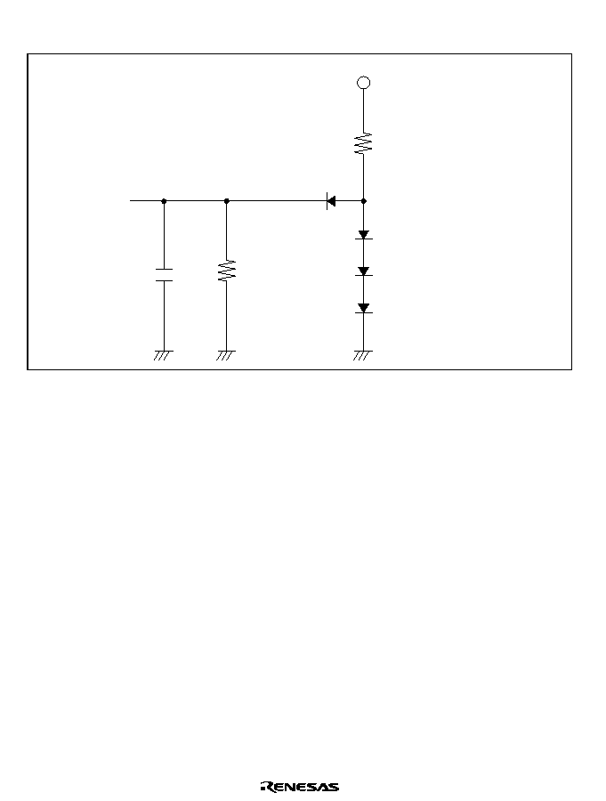
Rev. 2.0, 04/02, page 840 of 906
24.3
AC Characteristics
LSI output pin
C
RH
RL
3 V
C = 50 pF: ports A to H
C = 30 pF: ports 1 to 3,
P50 to P53,
ports 6 to 8
RL = 2.4 k
RH = 12 k
Input/output timing
measurement level:
1.5 V (V
CC
= 2.7 V to 3.6 V)
Figure 24.1 Output Load Circuit

Rev. 2.0, 04/02, page 841 of 906
Clock Timing
Table 24.5
Clock Timing
Conditions: V
CC
= 3.0 V to 3.6 V, AV
CC
= 3.0 V to 3.6 V, V
ref
= 3.0 V to AV
CC
, V
SS
= AV
SS
= 0 V,
¯ = 8 MHz to 33 MHz, T
a
= ≠20∞C to +75∞C (regular specifications),
T
a
= ≠40∞C to +85∞C (wide-range specifications)
Item
Symbol
Min
Max
Unit
Test Conditions
Clock cycle time
t
cyc
30.3
500
ns
Figure 24.2
Clock pulse high width
t
CH
10
--
ns
Figure 24.2
Clock pulse low width
t
CL
10
--
ns
Clock rise time
t
Cr
--
5
ns
Clock fall time
t
Cf
--
5
ns
Reset oscillation stabilization time
(crystal)
t
OSC1
10
--
ms
Figure 24.4 (1)
Software standby oscillation
stabilization time (crystal)
t
OSC2
10
--
ms
Figure 24.4 (2)
External clock output delay
stabilization time
t
DEXT
500
--
µ
s
Figure 24.4 (1)
Clock phase difference
*
t
cdif
1/4
◊
t
cyc
-
3 1/4
◊
t
cyc
+
3 ns
Figure 24.3
Clock pulse high width (SDRAM
)
*
t
SDCH
10
--
ns
Figure 24.3
Clock pulse low width (SDRAM
)
*
t
SDCL
10
--
ns
Figure 24.3
Clock rise time (SDRAM
)
*
t
sdcr
--
5
ns
Figure 24.3
Clock fall time (SDRAM
)
*
t
sdcf
--
5
ns
Figure 24.3
Note: Not supported in the H8S/2678 Series.
t
cyc
¯
t
CH
t
Cf
t
CL
t
Cr
Figure 24.2 System Clock Timing
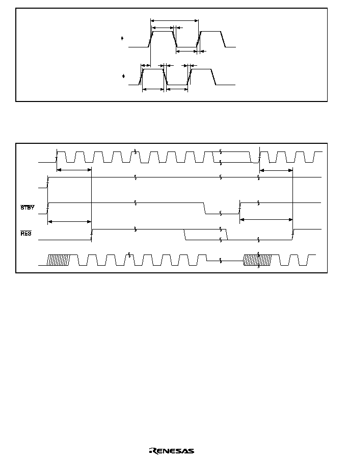
Rev. 2.0, 04/02, page 842 of 906
t
cyc
t
CH
t
Cf
t
CL
t
Cr
SDRAM
t
cdif
t
sdcf
t
sdcr
t
SDCH
t
SDCL
Figure 24.3 SDRAM
Timing*
Note:
Not supported in the H8S/2678 Series.
EXTAL
V
CC
¯
t
DEXT
t
OSC1
t
DEXT
t
OSC1
Figure 24.4 (1) Oscillation Stabilization Timing
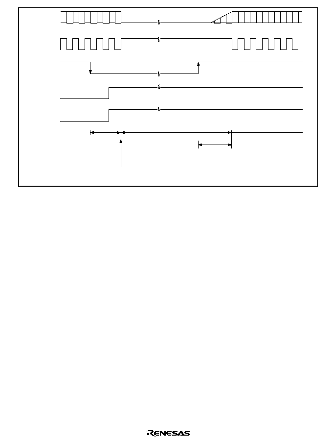
Rev. 2.0, 04/02, page 843 of 906
Oscillator
Software standby mode
(power-down mode)
Oscillation
stabilization time
t
OSC2
¯
NMI
NMI exception
handling
NMIEG = 1
SSBY = 1
NMI exception handling
SLEEP
instruction
NMIEG
SSBY
Figure 24.4 (2) Oscillation Stabilization Timing
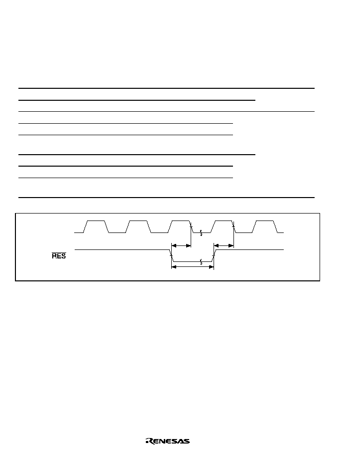
Rev. 2.0, 04/02, page 844 of 906
Control Signal Timing
Table 24.6
Control Signal Timing
Conditions: V
CC
= 3.0 V to 3.6 V, AV
CC
= 3.0 V to 3.6 V, V
ref
= 3.0 V to AV
CC
, V
SS
= AV
SS
= 0 V,
¯ = 8 MHz to 33 MHz, T
a
= ≠20∞C to +75∞C (regular specifications),
T
a
= ≠40∞C to +85∞C (wide-range specifications)
Item
Symbol
Min
Max
Unit
Test Conditions
5(6
setup time
t
RESS
200
--
ns
Figure 24.5
5(6
pulse width
t
RESW
20
--
t
cyc
NMI setup time
t
NMIS
150
--
ns
Figure 24.6
NMI hold time
t
NMIH
10
--
NMI pulse width (in recovery from
software standby mode)
t
NMIW
200
--
,54
setup time
t
IRQS
150
--
ns
,54
hold time
t
IRQH
10
--
,54
pulse width (in recovery from
software standby mode)
t
IRQW
200
--
¯
t
RESS
t
RESS
t
RESW
Figure 24.5 Reset Input Timing
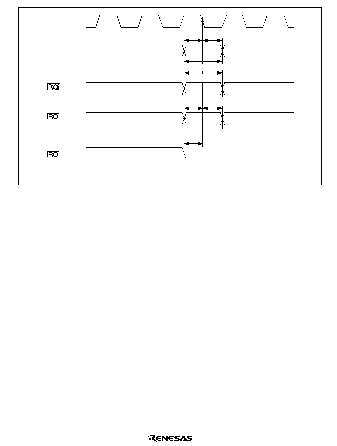
Rev. 2.0, 04/02, page 845 of 906
¯
NMI
(i = 0 to 15)
*
(edge input)
(level input)
Note:
*
Necessary for SSIER setting to clear software standby mode.
t
NMIS
t
NMIH
t
IRQS
t
IRQS
t
IRQH
t
NMIW
t
IRQW
Figure 24.6 Interrupt Input Timing

Rev. 2.0, 04/02, page 846 of 906
Bus Timing
Table 24.7
Bus Timing
Conditions: V
CC
= 3.0 V to 3.6 V, AV
CC
= 3.0 V to 3.6 V, V
ref
= 3.0 V to AV
CC
, V
SS
= AV
SS
= 0 V,
¯ = 8 MHz to 33 MHz, T
a
= ≠20∞C to +75∞C (regular specifications),
T
a
= ≠40∞C to +85∞C (wide-range specifications)
Item
Symbol
Min
Max
Unit
Test Conditions
Address delay time
t
AD
--
20
ns
Address setup time 1
t
AS1
0.5
◊
t
cyc
≠ 13
--
ns
Figures 24.7 to
24.21
Address setup time 2
t
AS2
1.0
◊
t
cyc
≠ 13
--
ns
Address setup time 3
t
AS3
1.5
◊
t
cyc
≠ 13
--
ns
Address setup time 4
t
AS4
2.0
◊
t
cyc
≠ 13
--
ns
Address hold time 1
t
AH1
0.5
◊
t
cyc
≠ 8
--
ns
Address hold time 2
t
AH2
1.0
◊
t
cyc
≠ 8
--
ns
Address hold time 3
t
AH3
1.5
◊
t
cyc
≠ 8
--
ns
&6
delay time 1
t
CSD1
--
15
ns
&6
delay time 2
t
CSD2
--
15
ns
&6
delay time 3
t
CSD3
--
20
ns
$6
delay time
t
ASD
--
15
ns
5'
delay time 1
t
RSD1
--
15
ns
5'
delay time 2
t
RSD2
--
15
ns
Read data setup time 1
t
RDS1
15
--
ns
Read data setup time 2
t
RDS2
15
--
ns
Read data hold time 1
t
RDH1
0
--
ns
Read data hold time 2
t
RDH2
0
--
ns
Read data access time 1
t
AC1
--
1.0
◊
t
cyc
≠ 20
ns
Read data access time 2
t
AC2
--
1.5
◊
t
cyc
≠ 20
ns
Read data access time 3
t
AC3
--
2.0
◊
t
cyc
≠ 20
ns
Read data access time 4
t
AC4
--
2.5
◊
t
cyc
≠ 20
ns
Read data access time 5
t
AC5
--
1.0
◊
t
cyc
≠ 20
ns
Read data access time 6
t
AC6
--
2.0
◊
t
cyc
≠ 20
ns
Read data access time 7
t
AC7
--
4.0
◊
t
cyc
≠ 20
ns
Read data access time 8
t
AC8
--
3.0
◊
t
cyc
≠ 20
ns
Address read data access time 1
t
AA1
--
1.0
◊
t
cyc
≠ 20
ns
Address read data access time 2
t
AA2
--
1.5
◊
t
cyc
≠ 20
ns
Address read data access time 3
t
AA3
--
2.0
◊
t
cyc
≠ 20
ns
Address read data access time 4
t
AA4
--
2.5
◊
t
cyc
≠ 20
ns
Address read data access time 5
t
AA5
--
3.0
◊
t
cyc
≠ 20
ns

Rev. 2.0, 04/02, page 847 of 906
Table 24.8
Bus Timing
Conditions: V
CC
= 3.0 V to 3.6 V, AV
CC
= 3.0 V to 3.6 V, V
ref
= 3.0 V to AV
CC
, V
SS
= AV
SS
= 0 V,
¯ = 8 MHz to 33 MHz, T
a
= ≠20∞C to +75∞C (regular specifications),
T
a
= ≠40∞C to +85∞C (wide-range specifications)
Item
Symbol
Min
Max
Unit
Test Conditions
:5
delay time 1
t
WRD1
--
15
ns
:5
delay time 2
t
WRD2
--
15
ns
Figures 24.7 to
24.21
:5
pulse width 1
t
WSW1
1.0
◊
t
cyc
≠ 13
--
ns
:5
pulse width 2
t
WSW2
1.5
◊
t
cyc
≠ 13
--
ns
Write data delay time
t
WDD
--
20
ns
Write data setup time 1
t
WDS1
0.5
◊
t
cyc
≠ 13
--
ns
Write data setup time 2
t
WDS2
1.0
◊
t
cyc
≠ 13
--
ns
Write data setup time 3
t
WDS3
1.5
◊
t
cyc
≠ 13
--
ns
Write data hold time 1
t
WDH1
0.5
◊
t
cyc
≠ 8
--
ns
Write data hold time 2
t
WDH2
1.0
◊
t
cyc
≠ 8
--
ns
Write data hold time 3
t
WDH3
1.5
◊
t
cyc
≠ 8
--
ns
Write command setup time 1
t
WCS1
0.5
◊
t
cyc
≠ 10
--
ns
Write command setup time 2
t
WCS2
1.0
◊
t
cyc
≠ 10
--
ns
Write command hold time 1
t
WCH1
0.5
◊
t
cyc
≠ 10
--
ns
Write command hold time 2
t
WCH2
1.0
◊
t
cyc
≠ 10
--
ns
Read command setup time 1
t
RCS1
1.5
◊
t
cyc
≠ 10
--
ns
Read command setup time 2
t
RCS2
2.0
◊
t
cyc
≠ 10
--
ns
Read command hold time
t
RCH
0.5
◊
t
cyc
≠ 10
--
ns
&$6
delay time 1
t
CASD1
--
15
ns
&$6
delay time 2
t
CASD2
--
15
ns
&$6
setup time 1
t
CSR1
0.5
◊
t
cyc
≠ 10
--
ns
&$6
setup time 2
t
CSR2
1.5
◊
t
cyc
≠ 10
--
ns
&$6
pulse width 1
t
CASW1
1.0
◊
t
cyc
≠ 20
--
ns
&$6
pulse width 2
t
CASW2
1.5
◊
t
cyc
≠ 20
--
ns
&$6
precharge time 1
t
CPW1
1.0
◊
t
cyc
≠ 20
--
ns
&$6
precharge time 2
t
CPW2
1.5
◊
t
cyc
≠ 20
--
ns
2(
delay time 1
t
OED1
--
15
ns
2(
delay time 2
t
OED2
--
15
ns
Precharge time 1
t
PCH1
1.0
◊
t
cyc
≠ 20
--
ns
Precharge time 2
t
PCH2
1.5
◊
t
cyc
≠ 20
--
ns

Rev. 2.0, 04/02, page 848 of 906
Item
Symbol
Min
Max
Unit
Test Conditions
Self-refresh precharge time 1
t
RPS1
2.5
◊
t
cyc
≠ 20
--
ns
Self-refresh precharge time 2
t
RPS2
3.0
◊
t
cyc
≠ 20
--
ns
Figure 24.22
Figure 24.23
:$,7
setup time
t
WTS
25
--
ns
Figure 24.15
:$,7
hold time
t
WTH
5
--
ns
%5(4
setup time
t
BREQS
30
--
ns
Figure 24.24
%$&.
delay time
t
BACD
--
15
ns
Bus floating time
t
BZD
--
40
ns
%5(42
delay time
t
BRQOD
--
25
ns
Figure 24.25
Address delay time 2
*
t
AD2
--
16.5
ns
Figure 24.26
CS delay time 4
*
t
CSD4
--
16.5
ns
Figure 24.26
DQM delay time
*
t
DQMD
--
16.5
ns
Figure 24.26
CKE delay time
*
t
CKED
--
16.5
ns
Figure 24.27
Read data setup time 3
*
t
RDS3
15
--
ns
Figure 24.26
Read data hold time 3
*
t
RDH3
0
--
ns
Figure 24.26
Write data delay time 2
*
t
WDD2
--
31.5
ns
Figure 24.26
Write data hold time 4
*
t
WDH3
2
--
ns
Figure 24.26
Note: Not supported in the H8S/2678 Series.
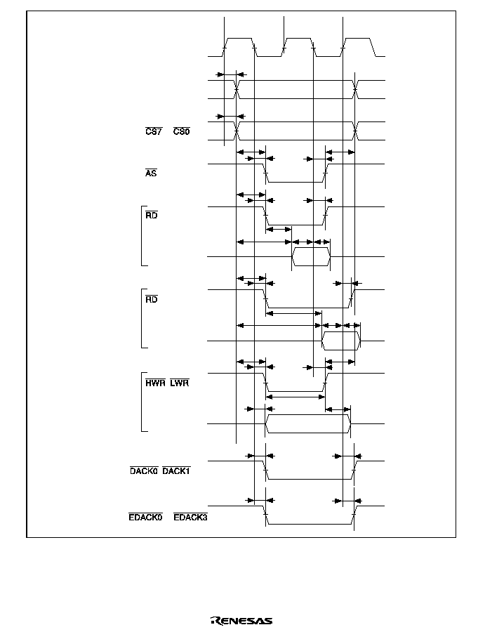
Rev. 2.0, 04/02, page 849 of 906
¯
T1
T2
A23 to A0
to
D15 to D0
D15 to D0
,
D15 to D0
Read
(RDNn = 1)
Read
(RDNn = 0)
Write
t
AD
t
CSD1
t
AS1
t
AS1
t
AS1
t
AS1
t
RSD1
t
RSD1
t
AC5
t
AA2
t
RSD1
t
WRD2
t
WSW1
t
WDH1
t
WDD
t
WRD2
t
AH1
t
AC2
t
RDS2
t
AA3
t
RSD2
t
RDS1
t
RDH1
t
AH1
t
ASD
t
ASD
,
to
t
DACD1
t
DACD2
t
EDACD1
t
EDACD2
t
RDH2
Figure 24.7 Basic Bus Timing: Two-State Access
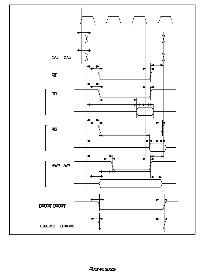
Rev. 2.0, 04/02, page 850 of 906
T1
¯
A23 to A0
to
D15 to D0
D15 to D0
,
D15 to D0
T2
T3
Read
(RDNn = 1)
Read
(RDNn = 0)
Write
t
AD
t
AS1
t
AH1
t
RSD1
t
RDS1
t
RDH1
t
RSD2
t
RDS2
t
RDH2
t
ASD
t
ASD
t
RSD1
t
RSD1
t
AC6
t
AC4
t
AA5
t
AS2
t
WSW2
t
WDS1
t
WRD1
t
WRD2
t
AH1
t
AA4
t
AS1
t
AS1
t
CSD1
,
to
t
DACD1
t
DACD2
t
EDACD1
t
EDACD2
t
WDH1
t
WDD
Figure 24.8 Basic Bus Timing: Three-State Access
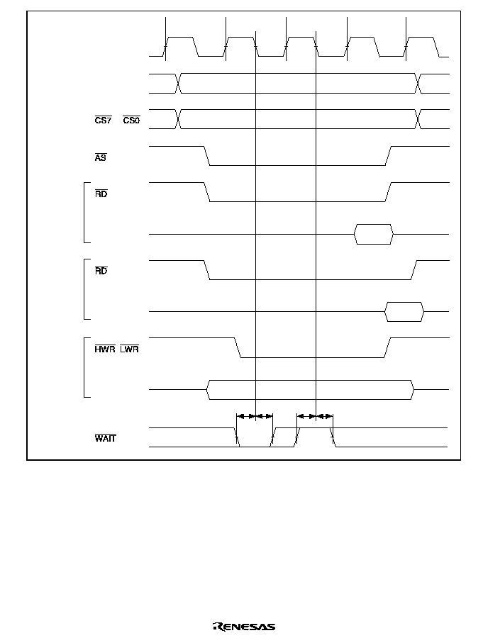
Rev. 2.0, 04/02, page 851 of 906
T1
¯
A23 to A0
to
D15 to D0
D15 to D0
,
D15 to D0
t
WTS
t
WTH
t
WTS
t
WTH
T2
Tw
T3
Read
(RDNn = 1)
Read
(RDNn = 0)
Write
Figure 24.9 Basic Bus Timing: Three-State Access, One Wait
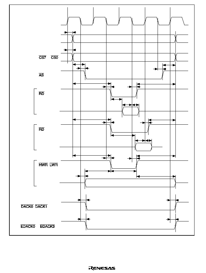
Rev. 2.0, 04/02, page 852 of 906
Th
t
AD
t
CSD1
t
AS1
t
ASD
t
AS3
t
RSD1
t
AC5
t
RDS1
t
RDH1
t
AH2
t
AH3
t
WDH3
t
WSW1
t
WDS2
t
WDD
t
AS3
t
WRD2
t
WRD2
t
RSD2
t
RSD1
t
AC2
t
RDS2
t
RDH2
t
AS3
t
RSD1
t
AH3
t
AH1
t
ASD
¯
A23 to A0
to
D15 to D0
D15 to D0
,
D15 to D0
T1
T2
Tt
Read
(RDNn = 1)
Read
(RDNn = 0)
Write
,
to
t
DACD1
t
DACD2
t
EDACD1
t
EDACD2
Figure 24.10 Basic Bus Timing: Two-State Access
(
$
$ Assertion Period Extended)
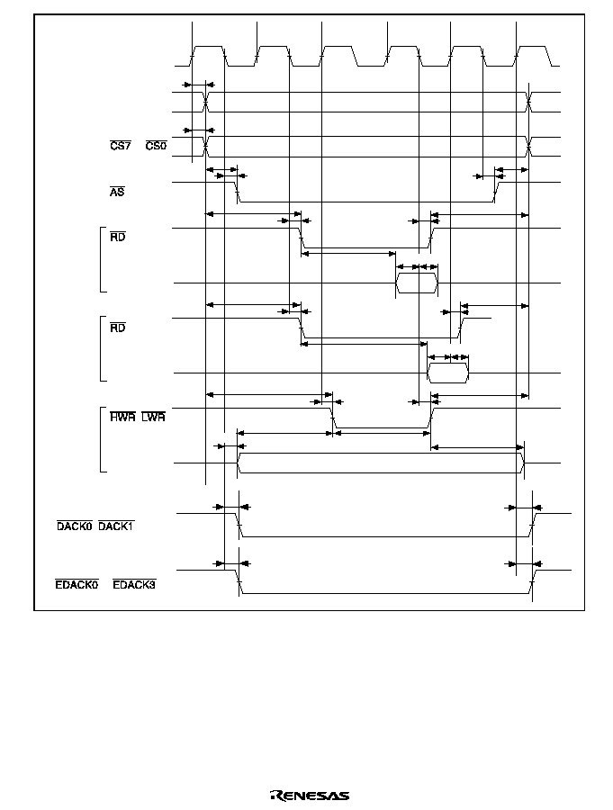
Rev. 2.0, 04/02, page 853 of 906
Th
t
AD
t
CSD1
t
AS1
t
ASD
t
AS3
t
RSD1
t
RSD1
t
ASD
t
AH1
t
AH3
t
AH2
t
AH3
t
WDH3
t
WSW2
t
WDS3
t
AS4
t
AS3
t
RSD1
t
WRD2
t
WRD1
t
AC4
t
RDH2
t
RSD2
t
AC6
t
RDH1
T1
T2
T3
Tt
¯
A23 to A0
to
D15 to D0
D15 to D0
D15 to D0
,
Read
(RDNn = 1)
Read
(RDNn = 0)
Write
,
to
t
DACD1
t
DACD2
t
EDACD1
t
EDACD2
t
RDS2
t
WDD
t
RDS1
Figure 24.11 Basic Bus Timing: Three-State Access
(
$
$ Assertion Period Extended)
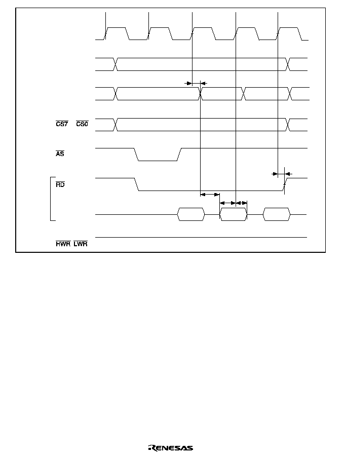
Rev. 2.0, 04/02, page 854 of 906
T1
¯
A23 to A6,
A0
A5 to A1
to
D15 to D0
,
T2
T1
t
AD
t
RSD2
t
AA1
t
RDS2
t
RDH2
T1
Read
Figure 24.12 Burst ROM Access Timing: One-State Burst Access
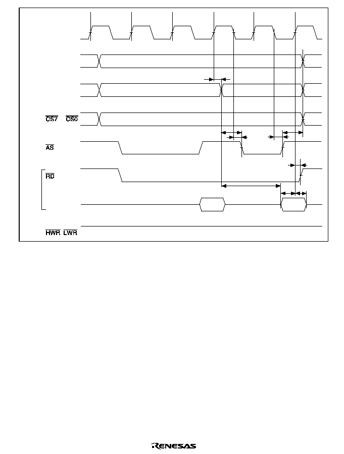
Rev. 2.0, 04/02, page 855 of 906
T1
¯
A23 to A6,
A0
A5 to A1
to
D15 to D0
,
T2
T3
T1
t
AD
t
AS1
t
ASD
t
AA3
t
RSD2
t
RDS2
t
RDH2
t
ASD
t
AH1
T2
Read
Figure 24.13 Burst ROM Access Timing: Two-State Burst Access
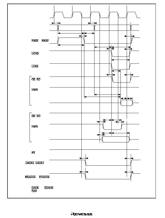
Rev. 2.0, 04/02, page 856 of 906
Tp
t
AD
t
AS3
t
AH1
t
CSD2
t
PCH2
t
AS2
t
AC1
t
OED1
t
OED1
t
AA3
t
AC4
t
WCS1
t
WCH1
t
WRD2
t
WDD
t
WDS1
t
WDH2
t
RDS2
t
RDH2
t
AH2
t
CSD3
t
CASD1
t
CASD1
t
CASW1
t
AD
¯
A23 to A0
to
,
D15 to D0
,
D15 to D0
Tr
Tc1
Tc2
Read
Write
,
to
t
DACD1
t
DACD2
t
EDACD1
t
EDACD2
Note:
and
timing: when DDS = 0 and EDDS = 0
timing: when RAST = 0
t
WRD2
Figure 24.14 DRAM Access Timing: Two-State Access
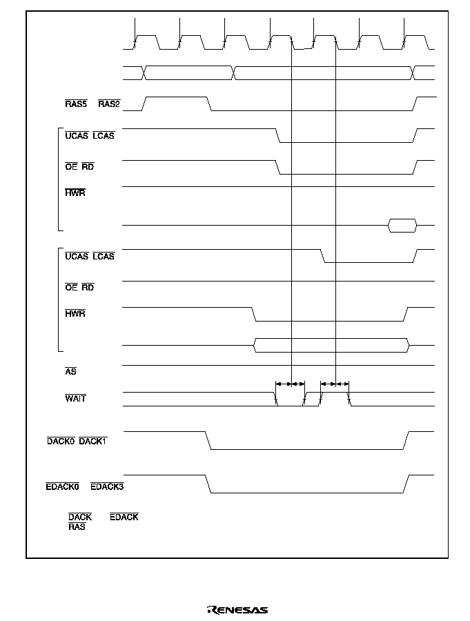
Rev. 2.0, 04/02, page 857 of 906
Tp
Tr
Tc1
Tcw
Tcwp
Tc2
¯
A23 to A0
to
,
,
D15 to D0
,
,
t
WTS
t
WTH
t
WTS
t
WTH
D15 to D0
Read
Write
Tcw : Wait cycle inserted by programmable wait function
Tcwp: Wait cycle inserted by pin wait function
,
to
and
timing: when DDS = 0 and EDDS = 0
timing: when RAST = 0
Note:
Figure 24.15 DRAM Access Timing: Two-State Access, One Wait
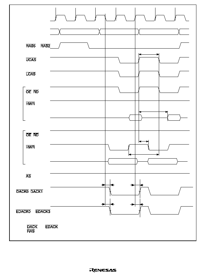
Rev. 2.0, 04/02, page 858 of 906
Tp
¯
A23 to A0
to
,
D15 to D0
,
D15 to D0
Tr
Tc1
t
CPW1
t
AC3
t
RCH
t
RCS1
Tc2
Tc1
Tc2
Read
Write
and
timing: when DDS = 1 and EDDS = 1
timing: when RAST = 0
Note:
,
to
t
DACD1
t
DACD2
t
EDACD1
t
EDACD2
Figure 24.16 DRAM Access Timing: Two-State Burst Access
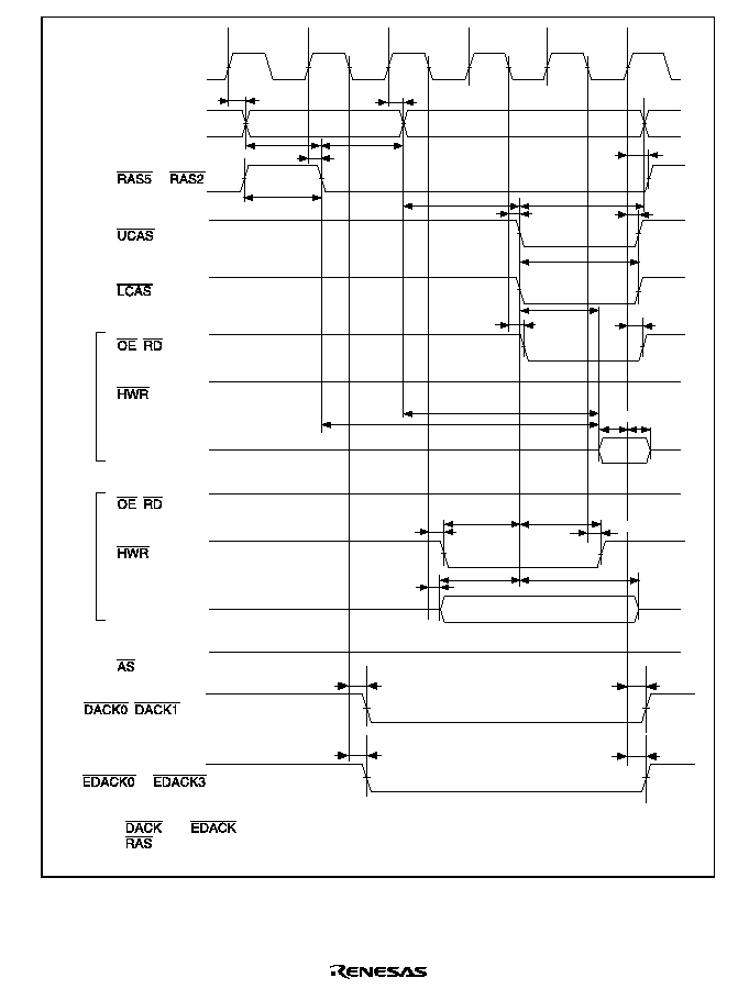
Rev. 2.0, 04/02, page 859 of 906
Tp
t
AD
t
AD
t
AS2
t
AH2
t
CSD2
t
PCH1
t
AS3
t
CSD3
t
CASD1
t
AH3
t
CASD2
t
CASW2
t
AC2
t
AA5
t
AC7
t
WRD2
t
WDD
t
WDS2
t
WDH3
t
WCS2
t
WCH2
t
RDH2
t
OED2
t
OED1
¯
A23 to A0
to
,
D15 to D0
,
D15 to D0
Tr
Tc1
Tc2
Tc3
Write
Read
and
timing: when DDS = 0 and EDDS = 0
timing: when RAST = 1
Note:
,
to
t
DACD1
t
DACD2
t
EDACD1
t
EDACD2
t
WRD2
t
RDS2
Figure 24.17 DRAM Access Timing: Three-State Access (RAST = 1)
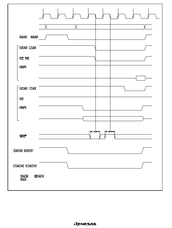
Rev. 2.0, 04/02, page 860 of 906
Tp
Tr
Tc1
Tcw
Tcwp
Tc2
Tc3
¯
A23 to A0
to
,
,
D15 to D0
,
t
WTS
t
WTH
t
WTS
t
WTH
D15 to D0
Read
Write
Tcw :
Wait cycle inserted by programmable wait function
Tcwp:
Wait cycle inserted by pin wait function
,
,
and
timing: when DDS = 0 and EDDS = 0
timing: when RAST = 0
Note:
Figure 24.18 DRAM Access Timing: Three-State Access, One Wait
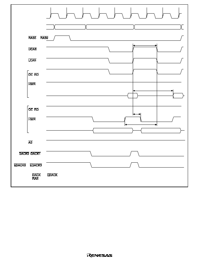
Rev. 2.0, 04/02, page 861 of 906
Tp
Tr
Tc1
Tc2
Tc3
Tc1
Tc2
Tc3
¯
A23 to A0
to
,
D15 to D0
,
t
RCH
t
RCS2
t
AC8
t
CPW2
D15 to D0
Read
Write
and
timing: when DDS = 1 and EDDS = 1
timing: when RAST = 1
Note:
,
to
Figure 24.19 DRAM Access Timing: Three-State Burst Access
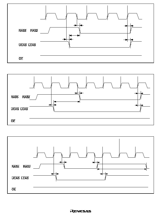
Rev. 2.0, 04/02, page 862 of 906
TRp
¯
to
,
TRr
t
CSD2
t
CSR1
t
CASD1
t
CASD1
t
CSD1
TRc1
TRc2
Figure 24.20 CAS-Before-RAS Refresh Timing
TRp
¯
to
,
TRrw
t
CSD2
t
CSR2
t
CASD1
t
CSD1
t
CASD1
TRr
TRc1
TRcw
TRc2
Figure 24.21 CAS-Before-RAS Refresh Timing (with Wait Cycle Insertion)
TRp
¯
to
,
TRr
t
CSD2
t
CASD1
t
CSD2
t
CASD1
t
RPS2
TRc
TRc
Tpsr
Tp
Tr
DRAM access
Self-refresh
Figure 24.22 Self-Refresh Timing
(Return from Software Standby Mode: RAST = 0)
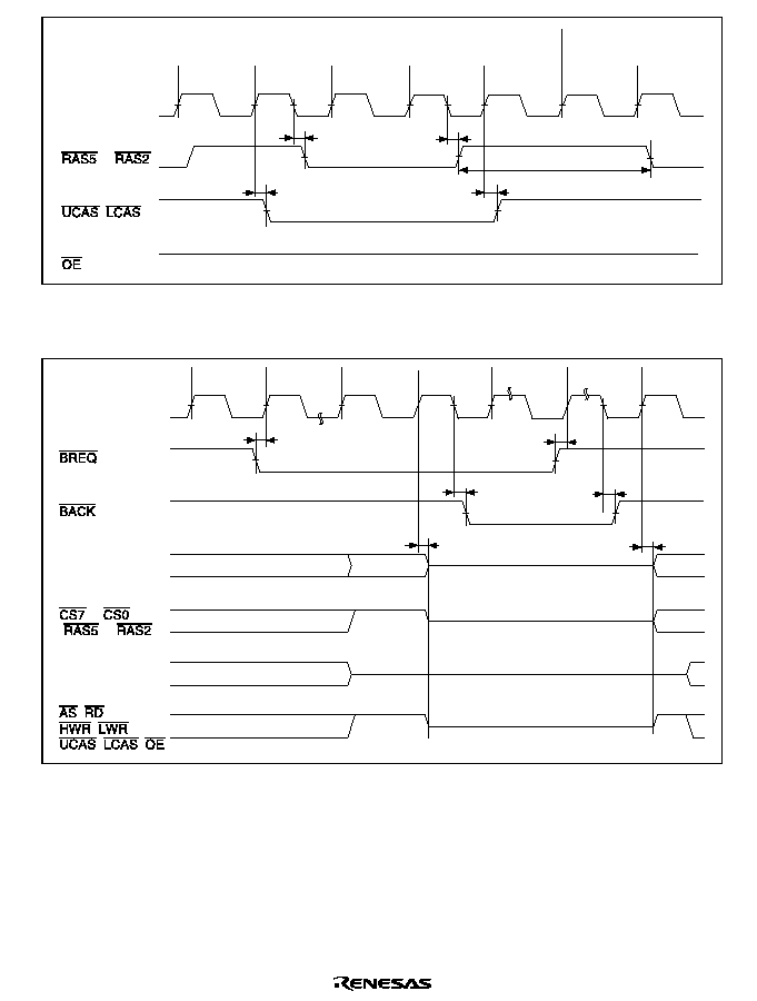
Rev. 2.0, 04/02, page 863 of 906
TRp
¯
to
,
TRr
t
CSD2
t
CASD1
t
CSD2
t
CASD1
t
RPS1
TRc
TRc
Tpsr
Tp
Tr
DRAM access
Self-refresh
Figure 24.23 Self-Refresh Timing
(Return from Software Standby Mode: RAST = 1)
¯
t
BREQS
t
BREQS
t
BACD
t
BZD
t
BACD
t
BZD
A23 to A0
to
(
to
)
D15 to D0
,
,
,
,
Figure 24.24 External Bus Release Timing
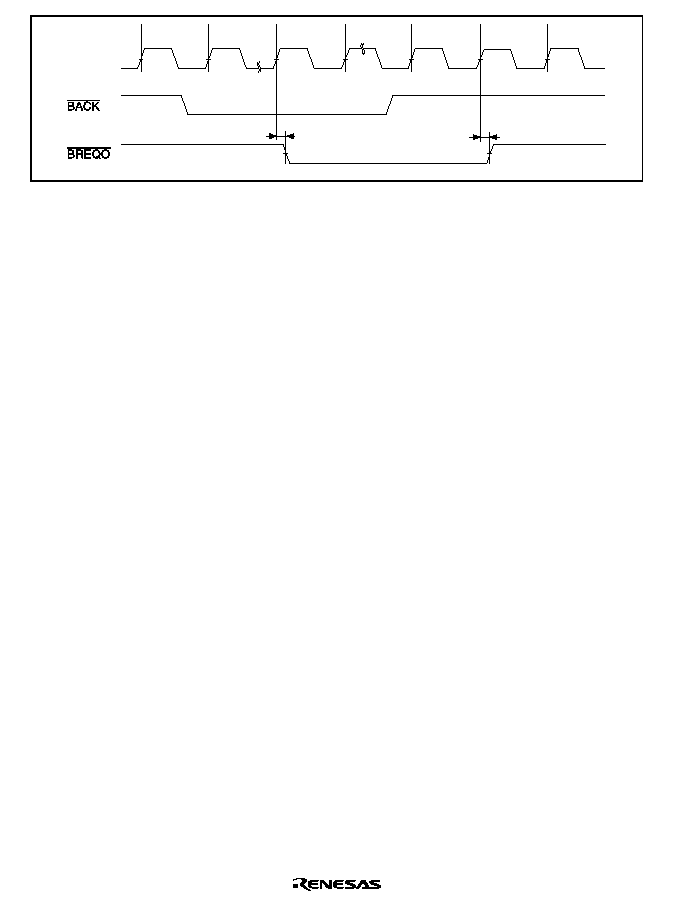
Rev. 2.0, 04/02, page 864 of 906
¯
t
BRQOD
t
BRQOD
Figure 24.25 External Bus Request Output Timing
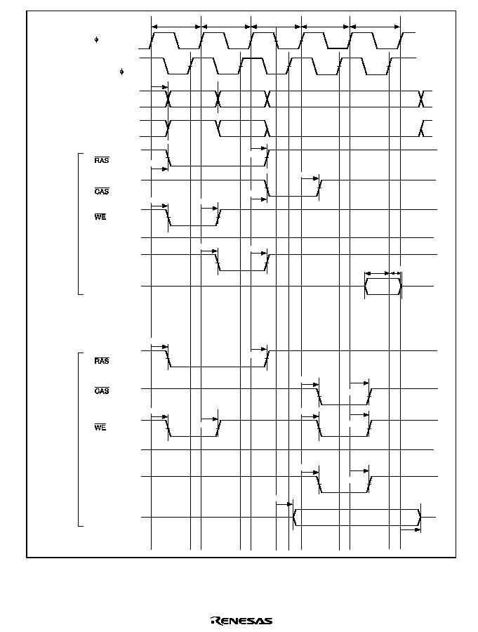
Rev. 2.0, 04/02, page 865 of 906
Tp
t
AD2
SDRAM
Address bus
Data bus
CKE
CKE
Precharge-sel
DQMU,
DQML
Data bus
DQMU,
DQML
Tr
Tc1
Tw
Tc2
Write
Read
t
CSD4
t
DQMD
t
RDS3
t
RDH3
t
CSD4
t
CSD4
t
CSD4
t
CSD4
t
CSD4
t
CSD4
t
CSD4
t
DQMD
t
CSD4
t
CSD4
t
CSD4
t
CSD4
t
DQMD
t
DQMD
t
WDD
t
WDH4
t
CSD4
t
CSD4
High
High
Figure 24.26 Synchronous DRAM Basic Access Timing (CAS Latency 2)
Note:
Not supported in the H8S/2678 Series.
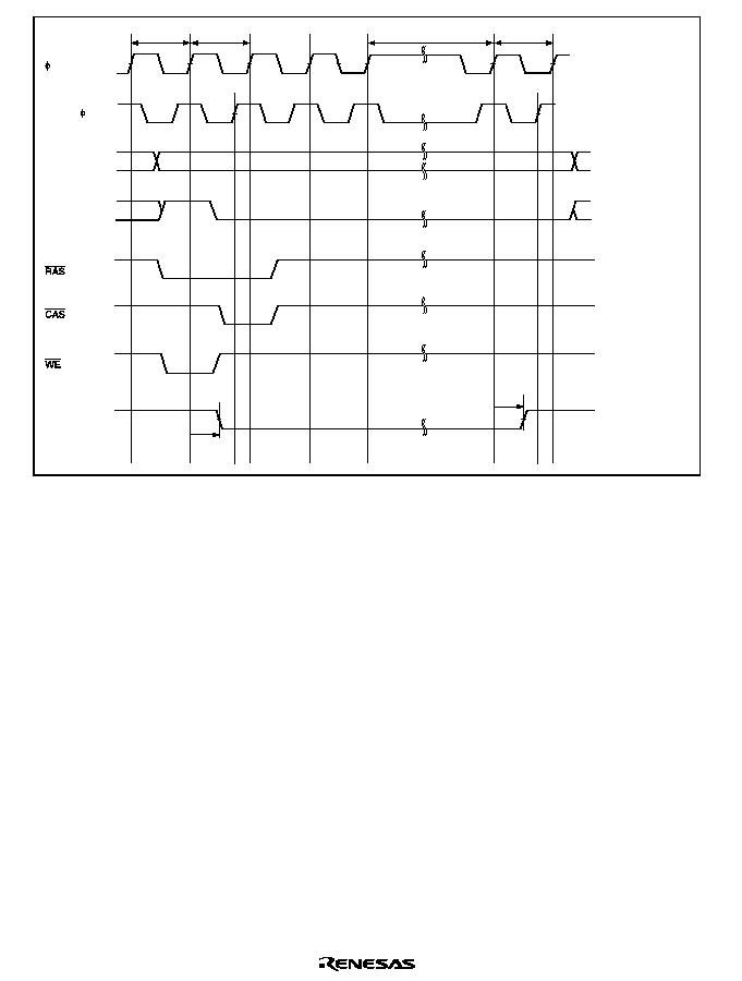
Rev. 2.0, 04/02, page 866 of 906
T
Rp
SDRAM
Address bus
Precharge-sel
CKE
T
Rr
T
Rr2
t
CKED
t
CKED
Software standby
Figure 24.27 Synchronous DRAM Self-Refresh Timing
Note:
Not supported in the H8S/2678 Series.
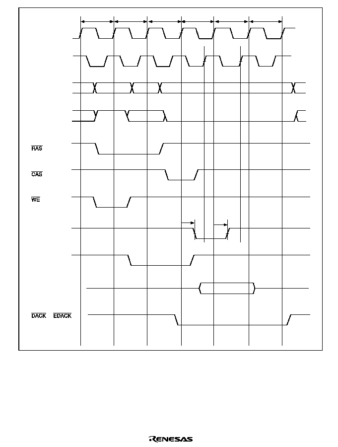
Rev. 2.0, 04/02, page 867 of 906
T
p
SDRAM
or
Address bus
Data bus
Precharge-sel
CKE
DQMU,
DQML
T
r
T
c1
T
c2
T
Rr
Ttp
2
t
CKED
t
CKED
Figure 24.28 Read Data: Two-State Expansion (CAS Latency 2)
Note:
Not supported in the H8S/2678 Series.

Rev. 2.0, 04/02, page 868 of 906
DMAC and EXDMAC Timing
Table 24.9
DMAC and EXDMAC Timing
Conditions: V
CC
= 3.0 V to 3.6 V, AV
CC
= 3.0 V to 3.6 V, V
ref
= 3.0 V to AV
CC
, V
SS
= AV
SS
= 0 V,
¯ = 8 MHz to 33 MHz, T
a
= ≠20∞C to +75∞C (regular specifications),
T
a
= ≠40∞C to +85∞C (wide-range specifications)
Item
Symbol
Min
Max
Unit
Test Conditions
'5(4
setup time
t
DRQS
25
--
ns
Figure 24.32
'5(4
hold time
t
DRQH
10
--
7(1'
delay time
t
TED
--
18
ns
Figure 24.31
'$&.
delay time 1
t
DACD1
--
18
Figure 24.29
'$&.
delay time 2
t
DACD2
--
18
Figure 24.30
('5(4
setup time
t
EDRQS
25
--
ns
Figure 24.32
('5(4
hold time
t
EDRQH
10
--
(7(1'
delay time
t
ETED
--
18
ns
Figure 24.31
('$&.
delay time 1
t
EDACD1
--
18
Figure 24.29
('$&.
delay time 2
t
EDACD2
--
18
Figure 24.30
('5$.
delay time
t
EDRKD
--
18
ns
Figure 24.33
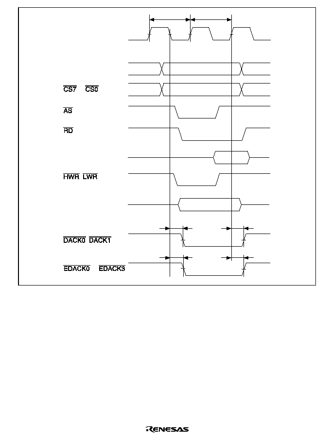
Rev. 2.0, 04/02, page 869 of 906
T1
¯
A23 to A0
to
t
DACD1
t
DACD2
t
EDACD1
t
EDACD2
(read)
D15 to D0
(read)
,
(write)
D15 to D0
(write)
,
to
T2
Figure 24.29 DMAC and EXDMAC Single Address Transfer Timing:
Two-State Access
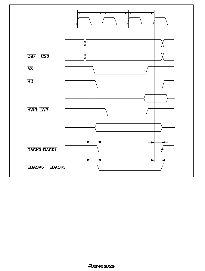
Rev. 2.0, 04/02, page 870 of 906
T1
t
DACD1
t
EDACD1
t
DACD2
t
EDACD2
¯
A23 to A0
to
(read)
D15 to D0
(read)
,
(write)
D15 to D0
(write)
,
to
T2
T3
Figure 24.30 DMAC and EXDMAC Single Address Transfer Timing:
Three-State Access
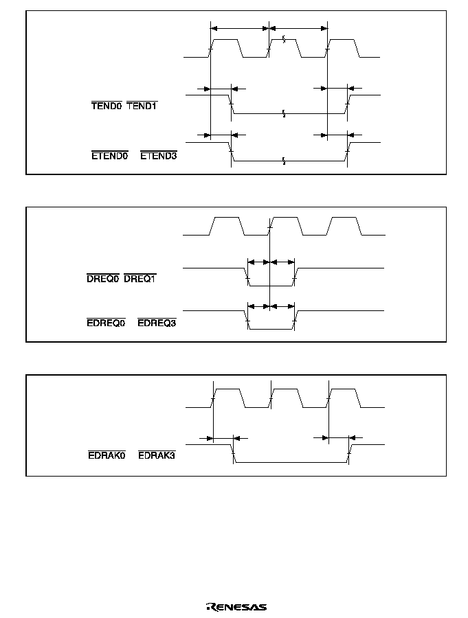
Rev. 2.0, 04/02, page 871 of 906
T1
t
TED
t
ETED
t
TED
t
ETED
¯
,
to
T2 or T3
Figure 24.31 DMAC and EXDMAC
7(1'
7(1'/((77(1'
(1' Output Timing
¯
,
t
DRQS
t
EDRQS
t
DRQH
t
DERQH
to
Figure 24.32 DMAC and EXDMAC
'
'55(4
(4/('
('55(4
(4 Input Timing
¯
to
t
EDRKD
t
EDRKD
Figure 24.33 EXDMAC
('5$.
('5$. Output Timing

Rev. 2.0, 04/02, page 872 of 906
Timing of On-Chip Peripheral Modules
Table 24.10 Timing of On-Chip Peripheral Modules
Conditions: V
CC
= 3.0 V to 3.6 V, AV
CC
= 3.0 V to 3.6 V, V
ref
= 3.0 V to AV
CC
, V
SS
= AV
SS
= 0 V,
¯ = 8 MHz to 33 MHz, T
a
= ≠20∞C to +75∞C (regular specifications),
T
a
= ≠40∞C to +85∞C (wide-range specifications)
Item
Symbol
Min
Max
Unit
Test Conditions
I/O ports
Output data delay time
t
PWD
--
40
ns
Figure 24.34
Input data setup time
t
PRS
25
--
ns
Input data hold time
t
PRH
25
--
ns
PPG
Pulse output delay time
t
POD
--
40
ns
Figure 24.35
TPU
Timer output delay time
t
TOCD
--
40
ns
Figure 24.36
Timer input setup time
t
TICS
25
--
ns
Timer clock input setup time
t
TCKS
25
--
ns
Figure 24.37
Single-edge
specification
t
TCKWH
1.5
--
t
cyc
Timer clock
pulse width
Both-edge
specification
t
TCKWL
2.5
--
t
cyc
8-bit timer Timer output delay time
t
TMOD
--
40
ns
Figure 24.38
Timer reset input setup time
t
TMRS
25
--
ns
Figure 24.40
Timer clock input setup time
t
TMCS
25
--
ns
Figure 24.39
Single-edge
specification
t
TMCWH
1.5
--
t
cyc
Timer clock
pulse width
Both-edge
specification
t
TMCWL
2.5
--
t
cyc
WDT
Overflow output delay time
t
WOVD
--
40
ns
Figure 24.41
SCI
Asynchronous
4
--
Figure 24.42
Input clock
cycle
Synchronous
t
Scyc
6
--
t
cyc
Input clock pulse width
t
SCKW
0.4
0.6
t
Scyc
Input clock rise time
t
SCKr
--
1.5
t
cyc
Input clock fall time
t
SCKf
--
1.5
Transmit data delay time
t
TXD
--
40
ns
Figure 24.43
Receive data setup time
(synchronous)
t
RXS
40
--
ns
Receive data hold time
(synchronous)
t
RXH
40
--
ns
A/D
converter
Trigger input setup time
t
TRGS
30
--
ns
Figure 24.44

Rev. 2.0, 04/02, page 873 of 906
T1
t
PRS
t
PRH
t
PWD
T2
¯
Ports 1 to 8, A to H
(read)
Ports 1 to 3, 6 to 9,
P53 to P50,
ports A to H
(write)
Figure 24.34 I/O Port Input/Output Timing
¯
PO15 to PO0
t
POD
Figure 24.35 PPG Output Timing
¯
Output compare
output
*
Input capture
input
*
t
TOCD
t
TICS
Note:
*
TIOCA0 to TIOCA5, TIOCB0 to TIOCB5, TIOCC0, TIOCC3, TIOCD0, TIOCD3
Figure 24.36 TPU Input/Output Timing
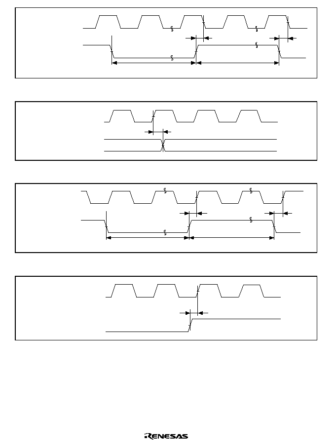
Rev. 2.0, 04/02, page 874 of 906
¯
TCLKA to TCLKD
t
TCKWL
t
TCKWH
t
TCKS
t
TCKS
Figure 24.37 TPU Clock Input Timing
¯
TMO0, TMO1
t
TMOD
Figure 24.38 8-Bit Timer Output Timing
¯
TMCI0, TMCI1
t
TMCWL
t
TMCWH
t
TMCS
t
TMCS
Figure 24.39 8-Bit Timer Clock Input Timing
¯
TMRI0, TMRI1
t
TMRS
Figure 24.40 8-Bit Timer Reset Input Timing
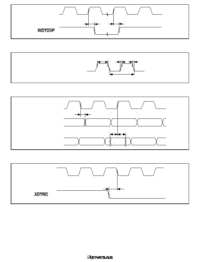
Rev. 2.0, 04/02, page 875 of 906
¯
t
WOVD
t
WOVD
Figure 24.41 WDT Output Timing
SCK0 to SCK2
t
SCKW
t
SCKr
t
SCKf
t
Scyc
Figure 24.42 SCK Clock Input Timing
SCK0 to SCK2
t
TXD
t
RXS
t
RXH
TxD0 to TxD2
(transmit data)
RxD0 to RxD2
(receive data)
Figure 24.43 SCI Input/Output Timing: Synchronous Mode
¯
t
TRGS
Figure 24.44 A/D Converter External Trigger Input Timing

Rev. 2.0, 04/02, page 876 of 906
24.4
A/D Conversion Characteristics
Table 24.11 A/D Conversion Characteristics
Conditions: V
CC
= 3.0 V to 3.6 V, AV
CC
= 3.0 V to 3.6 V, V
ref
= 3.0 V to AV
CC
, V
SS
= AV
SS
= 0 V,
¯ = 8 MHz to 33 MHz, T
a
= ≠20∞C to +75∞C (regular specifications),
T
a
= ≠40∞C to +85∞C (wide-range specifications)
Item
Min
Typ
Max
Unit
Resolution
10
10
10
Bit
Conversion time
--
--
8.1
µ
s
Analog input capacitance
--
--
20
pF
Permissible signal source impedance
--
--
5
k
Nonlinearity error
--
--
±7.5
LSB
Offset error
--
--
±7.5
LSB
Full-scale error
--
--
±7.5
LSB
Quantization error
--
±0.5
--
LSB
Absolute accuracy
--
--
±8.0
LSB
24.5
D/A Conversion Characteristics
Table 24.12 D/A Conversion Characteristics
Conditions: V
CC
= 3.0 V to 3.6 V, AV
CC
= 3.0 V to 3.6 V, V
ref
= 3.0 V to AV
CC
, V
SS
= AV
SS
= 0 V,
¯ = 8 MHz to 33 MHz, T
a
= ≠20∞C to +75∞C (regular specifications),
T
a
= ≠40∞C to +85∞C (wide-range specifications)
Item
Min
Typ
Max
Unit
Test Conditions
Resolution
8
8
8
Bit
Conversion time
--
--
10
µ
s
20 pF capacitive load
Absolute accuracy
--
±2.0
±3.0
LSB
2 M
resistive load
--
--
±2.0
LSB
4 M
resistive load

Rev. 2.0, 04/02, page 877 of 906
24.6
Flash Memory Characteristics
Table 24.13 Flash Memory Characteristics
Conditions: V
CC
= 3.0 V to 3.6 V, AV
CC
= 2.7 V to 3.6 V, V
ref
= 2.7 V to AV
CC
,
V
SS
= AV
SS
= 0 V, T
a
= 0∞C to 75∞C (program/erase operating temperature range:
regular specifications), T
a
= 0∞C to 85∞C (program/erase operating temperature
range: wide-range specifications)
Item
Symbol
Min
Typ
Max
Unit
Test
Conditions
Programming time
*
1,
*
2,
*
4
t
P
--
10
200
ms/
128 bytes
Erase time
*
1,
*
3,
*
6
t
E
--
50
1000
ms/
128 bytes
Rewrite times
N
WEC
--
--
100
Times
Programming Wait time after
SWE bit setting
*
1
x
1
--
--
µ
s
Wait time after
PSU bit setting
*
1
y
50
--
--
µ
s
Wait time after
P bit setting
*
1,
*
4
z
z1
--
--
30
µ
s
1
n
6
z2
--
--
200
µ
s
7
n
1000
z3
--
--
10
µ
s
Additional
program-
ming wait
Wait time after
P bit clearing
*
1
5
--
--
µ
s
Wait time after
PSU bit clearing
*
1
5
--
--
µ
s
Wait time after
PV bit setting
*
1
4
--
--
µ
s
Wait time after
H'FF dummy
write
*
1
2
--
--
µ
s
Wait time after
PV bit clearing
*
1
2
--
--
µ
s
Wait time after
SWE bit clearing
*
1
100
--
--
µ
s
Maximum number
of writes
*
1,
*
4
N
--
--
1000
*
5
Times

Rev. 2.0, 04/02, page 878 of 906
Item
Symbol
Min
Typ
Max
Unit
Test
Conditions
Erasing
Wait time after
SWE bit setting
*
1
x
1
--
--
µ
s
Wait time after
ESU bit setting
*
1
y
100
--
--
µ
s
Wait time after
E bit setting
*
1,
*
6
z
--
--
10
µ
s
Erase time
wait
Wait time after
E bit clearing
*
1
10
--
--
µ
s
Wait time after
ESU bit clearing
*
1
10
--
--
µ
s
Wait time after
EV bit setting
*
1
20
--
--
µ
s
Wait time after
H'FF dummy
write
*
1
2
--
--
µ
s
Wait time after
EV bit clearing
*
1
4
--
--
µ
s
Wait time after
SWE bit clearing
*
1
100
--
--
µ
s
Maximum number
of erases
*
1,
*
6
N
--
--
100
Times
Notes: 1. Follow the program/erase algorithms when making the time settings.
2. Programming time per 128 bytes. (Indicates the total time during which the P bit is set
in flash memory control register 1 (FLMCR1). Does not include the program-verify
time.)
3. Time to erase one block. (Indicates the time during which the E bit is set in FLMCR1.
Does not include the erase-verify time.)
4. Maximum programming time
t
P
(max) = wait time after P bit setting (z)
N
i=1
5. The maximum number of writes (N) should be set as shown below according to the
actual set value of (z) so as not to exceed the maximum programming time (t
P
(max)).
The wait time after P bit setting (z) should be changed as follows according to the
number of writes (n).
Number of writes (n)
1
n
6
z = 30 µs
7
n
1000
z = 200 µs
(Additional programming)
Number of writes (n)
1
n
6
z = 10 µs
6. For the maximum erase time (t
E
(max)), the following relationship applies between the
wait time after E bit setting (z) and the maximum number of erases (N):
t
E
(max) = Wait time after E bit setting (z)
◊
maximum number of erases (N)

Rev. 2.0, 04/02, page 879 of 906
24.7
Usage Note
The F-ZTAT and masked ROM versions both satisfy the electrical characteristics shown in this
manual, but actual electrical characteristic values, operating margins, noise margins, and other
properties may vary due to differences in manufacturing process, on-chip ROM, layout patterns,
and so on.
When system evaluation testing is carried out using the F-ZTAT version, the same evaluation
testing should also be conducted for the masked ROM version when changing over to that version.

Rev. 2.0, 04/02, page 880 of 906

Rev. 2.0, 04/02, page 881 of 906
Appendix
A.
I/O Port States in Each Pin State
Port Name
MCU
Operating
Mode*
1
Reset
Hardware
Standby
Mode
Software
Standby Mode
Bus Release
State
Program
Execution
State Sleep
Mode
Port 1
1 to 7
T
T
Keep
Keep
I/O port
Port 2
1 to 7
T
T
Keep
Keep
I/O port
P34 to P30
1 to 7
T
T
Keep
Keep
I/O port
P35/
2(
/
CKE
1 to 7
T
T
[OPE = 0,
2(
(CKE)
*
2
output]
T
[OPE = 1,
2(
(CKE)
*
2
output]
H
[Other than the
above]
Keep
[
2(
(CKE)
*
2
output]
T
[Other than the
above]
Keep
[
2(
(CKE)
*
2
output]
2(
(CKE)*
2
[Other than
the above]
I/O port
P47/DA1
1 to 7
T
T
[DAOE1 = 1]
Keep
[DAOE1 = 0]
T
Keep
Input port
P46/DA0
1 to 7
T
T
[DAOE0 = 1]
Keep
[DAOE0 = 0]
T
Keep
Input port
P45 to P40
1 to 7
T
T
T
T
Input port
P57/DA3
1 to 7
T
T
[DAOE3 = 1]
Keep
[DAOE3 = 0]
T
Keep
Input port
P56/DA2
1 to 7
T
T
[DAOE2 = 1]
Keep
[DAOE2 = 0]
T
Keep
Input port

Rev. 2.0, 04/02, page 882 of 906
Port Name
MCU
Operating
Mode*
1
Reset
Hardware
Standby
Mode
Software
Standby Mode
Bus Release
State
Program
Execution
State Sleep
Mode
P55, P54
1 to 7
T
T
T
T
Input port
P53 to P50
1 to 7
T
T
Keep
Keep
I/O port
Port 6
1 to 7
T
T
Keep
Keep
I/O port
Port 7
1 to 7
T
T
Keep
Keep
I/O port
Port 8
1 to 7
T
T
Keep
Keep
I/O port
PA7/A23
PA6/A22
PA5/A21
1 to 7
T
T
[OPE = 0,
address output]
T
[OPE = 1,
address output]
Keep
[Other than the
above]
Keep
[Address output]
T
[Other than the
above]
Keep
[Address
output]
A23 to A21
[Other than
the above]
I/O port
PA4/A20
PA3/A19
PA2/A18
PA1/A17
PA0/A16
1, 2, 5, 6
L
T
[OPE = 0]
T
[OPE = 1]
Keep
T
Address
output
A20 to A16
3, 4, 7
T
T
[OPE = 0,
address output]
T
[OPE = 1,
address output]
Keep
[Other than the
above]
Keep
[Address output]
T
[Other than the
above]
Keep
[Address
output]
A20 to A16
[Other than
the above]
I/O port
Port B
1, 2, 5, 6
L
T
[OPE = 0]
T
[OPE = 1]
Keep
T
Address
output
A15 to A8

Rev. 2.0, 04/02, page 883 of 906
Port Name
MCU
Operating
Mode*
1
Reset
Hardware
Standby
Mode
Software
Standby Mode
Bus Release
State
Program
Execution
State Sleep
Mode
Port B
3, 4
T
T
[OPE = 0,
address output]
T
[OPE = 1,
address output]
Keep
[Other than the
above]
Keep
[Address output]
T
[Other than the
above]
Keep
[Address
output]
A15 to A8
[Other than
the above]
I/O port
3, 7
T
T
[OPE = 0,
address output]
T
[OPE = 1,
address output]
Keep
[Other than the
above]
Keep
[Address output]
T
[Other than the
above]
Keep
[Address
output]
A15 to A8
[Other than
the above]
I/O port
Port C
1, 2, 5, 6
L
T
[OPE = 0]
T
[OPE = 1]
Keep
T
Address
output
A7 to A0
4
T
T
[OPE = 0,
address output]
T
[OPE = 1,
address output]
Keep
[Other than the
above]
Keep
[Address output]
T
[Other than the
above]
Keep
[Address
output]
A7 to A0
[Other than
the above]
I/O port

Rev. 2.0, 04/02, page 884 of 906
Port Name
MCU
Operating
Mode*
1
Reset
Hardware
Standby
Mode
Software
Standby Mode
Bus Release
State
Program
Execution
State Sleep
Mode
Port C
3, 7
T
T
[OPE = 0,
address output]
T
[OPE = 1,
address output]
Keep
[Other than the
above]
Keep
[Address output]
T
[Other than the
above]
Keep
[Address
output]
A7 to A0
[Other than
the above]
I/O port
Port D
1, 2, 4 to 6
T
T
T
T
D15 toD8
3, 7
T
T
[Data bus]
T
[Other than the
above]
Keep
[Data bus]
T
[Other than the
above]
Keep
[Data bus]
D15 to D8
[Other than
the above]
I/O port
Port E
1, 2,
4 to 6
8-bit
bus
T
T
Keep
Keep
I/O port
16-bit
bus
T
T
T
T
D7 to D0
3, 7
8-bit
bus
T
T
Keep
Keep
I/O port
16-bit
bus
T
T
[Data bus]
T
[Other than the
above]
Keep
[Data bus]
T
[Other than the
above]
Keep
[Data bus]
D7 to D0
[Other than
the above]
I/O port
1, 2, 4 to 6
Clock
output
PF7/¯
3, 7
T
T
[Clock output]
H
[Other than the
above]
Keep
[Clock output]
Clock output
[Other than the
above]
Keep
[Clock
output]
Clock output
[Other than
the above]
Input port

Rev. 2.0, 04/02, page 885 of 906
Port Name
MCU
Operating
Mode*
1
Reset
Hardware
Standby
Mode
Software
Standby Mode
Bus Release
State
Program
Execution
State Sleep
Mode
1, 2, 4 to 6
H
PF6/
$6
3, 7
T
T
[OPE = 0,
$6
output]
T
[OPE = 1,
$6
output]
H
[Other than the
above]
Keep
[
$6
output]
T
[Other than the
above]
Keep
[
$6
output]
$6
[Other than
the above]
I/O port
1, 2, 4 to 6
H
[OPE = 0]
T
[OPE = 1]
H
T
5'
,
+:5
PF5/
5'
PF4/
+:5
3, 7
T
T
[OPE = 0,
5'
,
+:5
output]
T
[OPE = 1,
5'
,
+:5
output]
H
[Other than the
above]
Keep
[
5'
,
+:5
output]
T
[Other than the
above]
Keep
[
5'
,
+:5
output]
5'
,
+:5
[Other than
the above]
I/O port
1, 2, 4 to 6
H
PF3/
/:5
3, 7
T
T
[OPE = 0,
/:5
output]
T
[OPE = 1,
/:5
output]
H
[Other than the
above]
Keep
[
/:5
output]
T
[Other than the
above]
Keep
[
/:5
output]
/:5
[Other than
the above]
I/O port

Rev. 2.0, 04/02, page 886 of 906
Port Name
MCU
Operating
Mode*
1
Reset
Hardware
Standby
Mode
Software
Standby Mode
Bus Release
State
Program
Execution
State Sleep
Mode
PF2/
/&$6
/
DQML*
2
1 to 7
T
T
[OPE = 0,
/&$6
(
'40/
)
output]
T
[OPE = 1,
/&$6
(
'40/
)
output]
H
[Other than the
above]
Keep
[
/&$6
(
'40/
)
output]
T
[Other than the
above]
Keep
[
/&$6
(
'40/
)
output]
/&$6
(
'40/
)
[Other than
the above]
I/O port
PF1/
8&$6
/
(
'408
)*
2
1 to 7
T
T
[OPE = 0,
8&$6
(
'408
)
output]
T
[OPE = 1,
8&$6
(
'408
)
output]
H
[Other than the
above]
Keep
[
8&$6
(
'408
)
output]
T
[Other than the
above]
Keep
[
8&$6
(
'408
)
output]
8&$6
[Other than
the above]
I/O port
PF0/
:$,7
1 to 7
T
T
[
:$,7
input]
T
[Other than the
above]
Keep
[
:$,7
input]
T
[Other than the
above]
Keep
[
:$,7
input]
:$,7
[Other than
the above]
I/O port
PG6/
%5(4
1 to 7
T
T
[
%5(4
input]
T
[Other than the
above]
Keep
[
%5(4
input]
%5(4
[
%5(4
input]
%5(4
[Other than
the above]
I/O port

Rev. 2.0, 04/02, page 887 of 906
Port Name
MCU
Operating
Mode*
1
Reset
Hardware
Standby
Mode
Software
Standby Mode
Bus Release
State
Program
Execution
State Sleep
Mode
PG5/
%$&.
1 to 7
T
T
[
%$&.
output]
T
[Other than the
above]
Keep
%$&.
[
%$&.
output]
%$&.
[Other than
the above]
I/O port
PG4/
%5(42
1 to 7
T
T
[
%5(42
output]
T
[Other than the
above]
Keep
[
%5(42
output]
%5(42
[Other than the
above]
Keep
[
%5(42
output]
%5(42
[Other than
the above]
I/O port
PG3/
&6
PG2/
&6
PG1/
&6
1 to 7
T
T
[OPE = 0,
&6
output]
T
[OPE = 1,
&6
output]
H
[Other than the
above]
Keep
[
&6
output]
T
[Other than the
above]
Keep
[
&6
output]
&6
[Other than
the above]
I/O port
1, 2, 5, 6
H
3, 4, 7
T
PG0/
&6
T
[OPE = 0,
&6
output]
T
[OPE = 1,
&6
output]
H
[Other than the
above]
Keep
[
&6
output]
T
[Other than the
above]
Keep
[
&6
output]
&6
[Other than
the above]
I/O port

Rev. 2.0, 04/02, page 888 of 906
Port Name
MCU
Operating
Mode*
1
Reset
Hardware
Standby
Mode
Software
Standby Mode
Bus Release
State
Program
Execution
State Sleep
Mode
PH3/
2(
/
CKE/
&6
1 to 7
T
T
[OPE = 0,
2(
output]
T
[OPE = 1,
2(
output]
H
[OPE = 0,
&6
output]
T
[OPE = 1,
&6
output]
H
[Other than the
above]
Keep
[
2(
output]
T
[
&6
output]
T
[Other than the
above]
Keep
[
2(
output]
2(
[
&6
output]
&6
[Other than
the above]
I/O port
PH2/
&6
1 to 7
T
T
[OPE = 0,
&6
output]
T
[OPE = 1,
&6
output]
H
[Other than the
above]
Keep
[
&6
output]
T
[Other than the
above]
Keep
[
&6
output]
&6
[Other than
the above]
I/O port
PH1/
&6
/
SDRAM
*
2
1 to 7
[DCTL
= 1]
Clock
output
[DCTL
= 0]
T
[DCTL = 1]
L
[DCTL = 0]
T
[DCTL = 1]
L
[DCTL = 0,
OPE = 0,
&6
output]
T
[DCTL = 0,
OPE = 1,
&6
output]
H
[Other than the
above]
Keep
[DCTL = 1]
Clock output
[DCTL = 0,
&6
output]
T
[Other than the
above]
Keep
[DCTL = 1]
Clock output
[DCTL = 0,
&6
output]
&6
[Other than
the above]
I/O port

Rev. 2.0, 04/02, page 889 of 906
Port Name
MCU
Operating
Mode*
1
Reset
Hardware
Standby
Mode
Software
Standby Mode
Bus Release
State
Program
Execution
State Sleep
Mode
PH0/
&6
1 to 7
T
T
[OPE = 0,
&6
output]
T
[OPE = 1,
&6
output]
H
[Other than the
above]
Keep
[
&6
output]
T
[Other than the
above]
Keep
[
&6
output]
&6
[Other than
the above]
I/O port
Legend:
L: Low level
H: High level
Keep: Input port becomes high-impedance, output port retains state
T: High impedance
DDR: Data direction register
OPE: Output port enable
Notes: 1. Mode 3 is not supported in the H8S/2678 Series.
2. Not available in the H8S/2678 Series.

Rev. 2.0, 04/02, page 890 of 906
B.
Product Lineup
Product
Type Name
Model Marking
Package (Code)
H8S/2676
Flash memory
version
HD64F2676
HD64F2676
144-pin QFP (FP-144G)
Masked ROM
version
HD6432676
HD64F2676(***)
144-pin QFP (FP-144G)
H8S/2675
Masked ROM
version
HD6432675
HD6432675(***)
144-pin QFP (FP-144G)
H8S/2674R
ROM-less
version
HD6412674R
HD6412674
144-pin LQFP (FP-144H)
H8S/2673
Masked ROM
version
HD6432673
HD6432673(***)
144-pin QFP (FP-144G)
H8S/2670
ROM-less
version
HD6412670
HD6412670
144-pin QFP (FP-144G)
[Symbols]
(***): ROM code
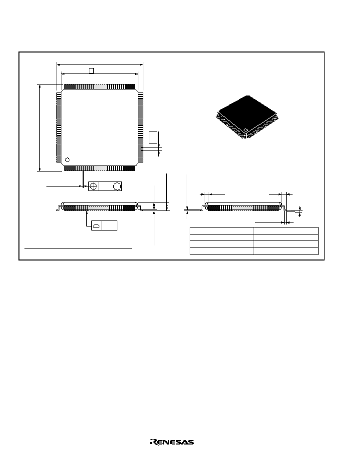
Rev. 2.0, 04/02, page 891 of 906
C.
Package Dimensions
For package dimensions, dimensions described in Hitachi Semiconductor Packages have priority.
Hitachi Code
JEDEC
JEITA
Mass (reference value)
FP-144H
--
Conforms
1.4 g
*Dimension including the plating thickness
Base material dimension
0.08
0.10
0.5
20
22.0 ± 0.3
108
73
109
72
37
144
1
36
22.0 ± 0.3
1.0
0.5 ± 0.1
1.70 Max
1.45
0.12 ± 0.08
0∞ ≠ 8∞
M
*0.17 ± 0.05
*0.22 ± 0.05
1.25
0.20 ± 0.04
0.15 ± 0.04
As of July, 2001
Unit: mm
Figure C.1 Package Dimensions (FP-144H)
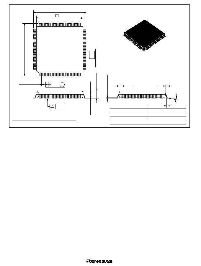
Rev. 2.0, 04/02, page 892 of 906
Hitachi Code
JEDEC
JEITA
Mass (reference value)
FP-144G
--
Conforms
2.4 g
*Dimension including the plating thickness
Base material dimension
0.10 M
20
22.0 ± 0.2
73
36
144
0.5
0.10
3.05 Max
0∞ ≠ 8∞
22.0 ± 0.2
108
72
37
109
1
0.17 ± 0.05
2.70
0.22 ± 0.05
0.5 ± 0.1
1.0
0.10
+0.15
≠0.10
1.25
0.20 ± 0.04
0.15 ± 0.04
*
*
As of July, 2001
Unit: mm
Figure C.2 Package Dimensions (FP-144G)
Rev. 2.0, 04/02, page 893 of 906
Main Revisions and Additions in this Edition
Item
Page
Revisions (See Manual for Details)
1.1 Features
1
The following product deleted.
Model: HD64F2677R
3.4 Memory Map in Each
Operating Mode
65
Address map for H8S/2677R deleted.
5.3.1 Interrupt Control
Register (INTCR)
Bits 7 to 6
88
Bit
R/W
Description
7
6
R/W
R/W
Reserved
These bits can be read from or written to.
However, the write value should always be 0.
5.3.1 Interrupt Control
Register (INTCR)
Bits 2 to 0
88
Bit
R/W
Description
2 to
0
R/W
Reserved
These bits can be read from or written to.
However, the write value should always be 0.
5.7.6 Note on IRQ Status
Register (ISR)
118
Section 5.7.6 added.
6.3.7 Bus Control
Register (BCR)
134
Description changed.
Bit 15: External Bus Release Enable
6.3.7 Bus Control
Register (BCR)
134
Description changed.
Bit 13: This bit can be read from or written to. However, the
write value should always be 0.
6.3.8 DRAM Control
Register (DRAMCR)
136
Descriptions changed.
Bits 13, 11, 3: This bit can be read from or written to.
However, the write value should always be 0.
6.3.9 DRAM Access
Control Register
(DRACCR)
143 to
145
Descriptions changed.
H8S/2678 Series
Bit 6: This bit can be read from or written to. However, the
write value should always be 0.
H8S/2678R Series
Bits 14, 10, 7 to 4, 2: This bit (These bits) can be read from or
written to. However, the write value should always be 0.
Figure 6.5 CAS Latency
Control Cycle Disable
Timing during Continuous
Synchronous DRAM
Space Write Access (for
CAS Latency 2)
146
Error in figure 6.5 corrected.
(Error)
'408
,
'40/
(Correction) DQMU, DQML
6.3.10 Refresh Control
Register (REFCR)
148
Description changed.
Bit 11: This bit can be read from or written to. However, the
write value should always be 0.

Rev. 2.0, 04/02, page 894 of 906
Item
Page
Revisions (See Manual for Details)
7.3.4 DMA Control
Registers (DMACRA and
DMACRB)
Full Address Mode
266
Description of DMACR changed.
Bits 10 to 8, 7, 4: This bit (These bits) can be read from or
written to. However, the write value should always be 0.
7.3.4 DMA Control
Registers (DMACRA and
DMACRB)
Full Address Mode
DMACR_0B and
DMACR_1B
267
Desctiption of bits DTF3 to DTF0 added.
0010: Activated by
'5(4
pin falling edge input (detected as
a low level in the first transfer after transfer is enabled)
7.3.5
DMA Band
Control Registers H and L
(DMABCRH and
DMABCRL)
Full Address Mode
271 to
273
Descriptions of DMABCRH changed.
Bits 13, 12, 10, 8: This bit (These bits) can be read from or
written to. However, the write value should always be 0.
7.3.5 DMA Band Control
Registers H and L
(DMABCRH and
DMABCRL)
Full Address Mode
277,
278
Descriptions of bits 3 to 0 in DMABCRL changed.
Bit 3: (Error) If the DTIE1B bit is set to 1 when DTME1 = 0,
(Correction) If the DTME1 bit is cleared to 0 when DTIE1B =
1,
Bit 2: (Error) If the DTIE1A bit is set to 1 when DTE1 = 0,
(Correction) If the DTE1 bit is cleared to 0 when DTIE1A= 1,
Bit 1: (Error) If the DTIE0B bit is set to 1 when DTME0 = 0,
(Correction) If the DTME0 bit is cleared to 0 when DTIE0B=
1,
Bit 0: (Error) If the DTIE0A bit is set to 1 when DTE0 = 0,
(Correction) If the DTE0 bit is cleared to 0 when DTIE0A = 1,
7.3.7 DMA Terminal
Control Register
(DMATCR)
281
Description on DMATCR added.
7.4.1 Activation by
Internal Interrupt Request
283
With ADI, TXI, and RXI interrupts,
...
When an interrupt request signal for DMAC activation is also
used for an interrupt request to the CPU or DTC activation
(DTA = 0),
7.5.11 Write Data Buffer
Function
319
DMAC internal-to-external dual address transfers and single
address transfers can be executed
...
...
, dual address transfer external write cycles or single
transfer and internal accesses
...
8.3.4 EXDMA Mode
Control Register (EDMDR)
340
Desription changed.
Bits 1, 0: These bits are always read as 0. The initial values
should not be modified.
9.2.6 DTC Transfer
Count Register B (CRB)
397
Description added.
This register is not available in normal and repeat modes.

Rev. 2.0, 04/02, page 895 of 906
Item
Page
Revisions (See Manual for Details)
10.1.4 Pin Functions
P17/PO15/TIOCB2/TCLK
D/
('5$.
425
TPU channel 2
settings
(2)
(1)
(2)
MD3 to MD0
IOB3 to IOB0
B'0011
B'xx00
Other than B'xx00
10.1.4 Pin Functions
P15/PO13/TIOCB1/
TCLKC
426
Notes amended.
(Error) TIOCB1 input when MD3 to MD0 = B'0000 or B'01XX
and IOB3 = B'10xx.
(Correction) TIOCB1 input when MD3 to MD0 = B'0000 or
B'01xx and IOB3 to IOB0 = B'10xx.
10.1.4 Pin Functions
P14/PO12/TIOCA1
427
Notes amended.
(Error) TIOCA1 input when MD3 to MD0 = B'0000, B'000,
and B'01xx and IOA3 = B'10xx.
(Correction) TIOCA1 input when MD3 to MD0 = B'0000 or
B'01xx and IOA3 to IOA0 = B'10xx.
10.2.4 Pin Functions
P27/PO7/TIOCB5/(
,54
)/
('5$.
434
The values of MD3 to MD0 in the subordinated table
amended.
(Error) B'0000 to B'0011
(Correction) B'0000, B'01xx
10.2.4 Pin Functions
P26/PO6/TIOCA5/(
,54
)
/
('5$.
435
The following values in the subordinated table amended.
MD3 to MD0: (Error) B'0000 to B'0011
(Correction)
B'0000, B'01xx
MD3 to MD0: (Error) B'0010
(Correction) B'001x
CCLR1, CCLR0: (Error) Other than B'10
(Correction)
Other than B'01
CCLR1, CCLR0: (Error) B'10
(Correction) B'01
10.2.4 Pin Functions
P25/PO5/TIOCB4/(
,54
)
436
The values of MD3 to MD0 in the subordinated table
amended.
(Error) B'0000 to B'0011
(Correction) B'0000, B'01xx
10.2.4 Pin Functions
P24/PO4/TIOCA4/
RxD4/(
,54
)
437
The following values in the subordinated table amended.
MD3 to MD0: (Error) B'0000 to B'0011
(Correction)
B'0000, B'01xx
CCLR1, CCLR0: (Error) Other than B'10
(Correction)
Other than B'01
CCLR1, CCLR0: (Error) B'10
(Correction) B'01
10.2.4 Pin Functions
P23/PO3/TIOCD3/TxD4/
(
,54
)
438
The values of MD3 to MD0 in the subordinated table
amended.
(Error) B'0001 to B'0011
(Correction) B'0000
10.2.4 Pin Functions
P22/PO2/TIOCC3/(
,54
)
439
The values of MD3 to MD0 in the subordinated table
amended.
(Error) B'0001 to B'01xx
(Correction) B'0000
Rev. 2.0, 04/02, page 896 of 906
Item
Page
Revisions (See Manual for Details)
10.2.4 Pin Functions
P21/PO1/TIOCB3/(
,54
)
440
The values of MD3 to MD0 in the subordinated table
amended.
(Error) B'0001 to B'0011
(Correction) B'0000
10.2.4 Pin Functions
P20/PO0/TIOCA3/(
,54
)
441
The values of MD3 to MD0 in the subordinated table
amended.
(Error) B'0001 to B'01xx
(Correction) B'0000
10.3.6 Pin Functions
P35/SCK1/SCL0/(
2(
)/
(CKE
*3
)
444
(Correction)
...
bits CKE0 and CKE1 in SCR, bits OEE and
RMTS2 to RMTS0 in DRAMCR, bit OES in PFCR2, and bit
P35DDR.
10.6.4 Pin Functions
P63/TMCI1/
7(1'
/
,54
456
Note added.
When used as the external clock input pin for the TMR, its pin
function should be specified to the external clock input by the
CKS2 to CKS0 bits in TCR_1.
10.6.4 Pin Functions
P62/TMCI0/
7(1'
/
,54
456
Note added.
When used as the external clock input pin for the TMR, its pin
function should be specified to the external clock input by the
CKS2 to CKS0 bits in TCR_1.
10.6.4 Pin Functions
P61/TMRI1/
'5(4
/
,54
457
Note added.
When used as the counter reset input pin for the TMR, both
the CCLR1 and CCLR0 bits in TCR_1 should be set to 1.
10.6.4 Pin Functions
P60/TMRI0/
'5(4
/
,54
457
Note added.
When used as the counter reset input pin for the TMR, both
the CCLR1 and CCLR0 bits in TCR_1 should be set to 1.
10.14.4 Pin Functions
PF0/
:$,7
491
(Correction)
...
bit EXPE, bit WAITE in BCR, and bit PF0DDR.
10.15.5 Pin Functions
PG3/CS3/RAS3*/CAS*,
PG2/CS2/RAS2*/RAS*
496
Operating
mode
3
*
, 7
PGnDDR
0
Pin function PGn
input
1
PGn
output
0
PGn
input
1
PGn
output
0
PGn
input
1
output output output output
*
*
14.6.2 Contention
between Timer Counter
(TCNT) Write and
Increment
629
If a timer counter clock pulse is generated during the next
cycle after the T2 state of a TCNT write cycle,
16.3.2 I2C Bus Control
Register B (ICCRB)
714
Bit
Description
5
A/D Start
Clearing this bit to 0 stops A/D conversion, and
the A/D converter enters wait state. When this bit
is set to 1 by software, TPU (trigger), TMR
(trigger), or the ADTRG pin, A/D conversion starts.
This bit remains set to 1 during A/D conversion. In
single mode, cleared to 0 automatically when
conversion on the specified channel ends. In
scan mode, conversion continues sequentially on
the specified channels until this bit is cleared to 0
by a reset, or a transition to hardware standby
mode or software.

Rev. 2.0, 04/02, page 897 of 906
Item
Page
Revisions (See Manual for Details)
16.4.2 Scan Mode
721
Description added to item 4.
If the ADST bit is later set to 1, A/D conversion starts again
from the first channel in the group.
Section 18 RAM
739
The following product of the H8S/2678R Series deleted.
Product type name: H8S/2677R
19.1 Features
741
The following product of the H8S/2678R Series deleted.
Product type name: H8S/2677R
19.5.2 Flash Memory
Control Register 2
(FLMCR2)
751
Description added.
When the on-chip flash memory is disabled, the contents of
FLMCR2 are always read as H'00.
19.6 On-Board
Programming Modes
756
Description amended.
19.6.1 Boot Mode
756
Description amended.
19.6.1 Boot Mode
Table 19.6 System Clock
Frequencies for which
Automatic Adjustment of
LSI Bit Rate is Possible
758
Table 19.6 amended.
19,200 bps
(Correction) 8 to 25 MHz
9,600 bps
(Correction) 8 to 25 MHz
4,800 bps
(Correction) deleted
19.8.1 Program/Program-
Verify
762
4. Consecutively transfer 128 bytes of data in byte units from
the programming data area,
21.1.1 System Clock
Control Register (SCKCR)
778
Description of bit 6 amended.
This bit can be read from or written to. However, The write
value should always be 0.
21.1.2 PLL Control
Register (PLLCR)
779
Description of bit 3 amended.
This bit can be read from or written to. However, The write
value should always be 0.
21.2.2 External Clock
Input
Table 21.3 External Clock
Input Conditions
782
Item
External clock input
low pulse width
External clock input
high pulse width
Min
Max
Vcc = 3.0 V
to 3.6 V
15
15
21.5.2 Notes on
Resonator
783
As the parameters for the oscillation circuit will depend on the
floating capacitance of the resonator and the user board, the
parameters should be determined in consultation with the
resonator manufacturer.

Rev. 2.0, 04/02, page 898 of 906
Item
Page
Revisions (See Manual for Details)
23.3 Register States in
Each Operating Mode
826
Register
Abbreviation
P1DDR
P2DDR
PAODR
Reset
High-Speed
Clock
Division
Hardware
Standby
Initialized
Initialized
Sleep
Initialized
23.3 Register States in
Each Operating Mode
829,
830
Register
Abbreviation
PORT1
PORT2
PORTG
Reset
High-Speed
Clock
Division
Hardware
Standby
Sleep
23.3 Register States in
Each Operating Mode
831,
832
Register
Abbreviation
TCR_0
TCR_1
TCNT
Reset
Initialized
Initialized
High-Speed
Clock
Division
Hardware
Standby
Initialized
Initialized
Sleep
Initialized
Initialized
RSTCSR
Initialized
Section 24 Electrical
Characteristics
836
TBD deleted.
24.2 DC Characteristics
Table 24.2 DC
Characteristics
836,
837
Pin added.
Input high voltage:
67%<
, MD2 to MD0, DCTL
*
4
Input low voltage:
5(6
,
67%<
, MD2 to MD0, DCTL
*
4
Input leakage current:
67%<
, NMI, MD2 to MD0, DCTL
*
4
24.3 AC Characteristics
Figure 24.4 (1) Oscillation
Stabilization Timing
842
All timing stipulated at 1/2 Vcc.
24.3 AC Characteristics
Table 24.8 Bus Timing
848
Item
Address delay time 2
*
CS delay time 4
*
Symbol
tAD2
tCSD4
Min
Max
16.5
16.5
Test Conditions
Figure 24.26
Figure 24.26
Unit
ns
ns
Read data setup time 3
*
tRDS3
15
Figure 24.26
ns
Read data hold time 3
*
Write data delay time 2
*
tRDH3
tWDD2
0
31.5
Figure 24.26
Figure 24.26
ns
ns
Write data hold time 4
*
tWDH3
2
Figure 24.26
ns
24.3 AC Characteristics
Figure 24.26
Synchronous DRAM Basic
Access Timing (CAS
Latency 2)
Figure 24.27
Synchronous DRAM Self-
Refresh Timing
Figure 24.28 Read Data:
Two-State Expansion
(CAS Latency 2)
865 to
867
All timing stipulated at 1/2 Vcc.
Rev. 2.0, 04/02, page 899 of 906
Item
Page
Revisions (See Manual for Details)
A.
I/O Port States in
Each Pin State
881
Port Name
P35/
/
CKE
Software
Standby Mode
[OPE = 0,
(
)
*
2
output]
T
[OPE = 1,
(
)
*
2
output]
H
[Other than the
above]
Keep
[
(
)
*
2
output]
T
[Other than the
above]
Keep
[
(
)
*
2
output]
(CKE)
*
2
[Other than
the above]
I/O port
Bus Release
State
Program
Execution
State Sleep
Mode
A.
I/O Port States in
Each Pin State
888
Port Name
Reset
PH3/
/
CKE/
Software
Standby Mode
Hardware
Standby
Mode
[OPE = 0,
output]
T
[OPE = 1,
output]
H
[OPE = 0,
output]
T
[OPE = 1,
output]
H
[Other than the
above]
Keep
MCU
Operating
Mode
1 to 7
T
T
[
output]
T
[
output]
T
[Other than the
above]
Keep
[
output]
[
output]
[Other than
the above]
I/O port
Bus Release
State
Program
Execution
State Sleep
Mode
PH1/
/
SDRAM
*
2
[DCTL = 1]
L
[DCTL = 0,
OPE = 0,
output]
T
[DCTL = 0,
OPE = 1,
output]
H
[Other than the
above]
Keep
1 to 7
[DCTL
= 1]
Clock
output
[DCTL
= 0]
T
[DCTL = 1]
L
[DCTL = 0]
T
[DCTL = 1]
Clock output
[DCTL = 0,
output]
T
[Other than the
above]
Keep
[DCTL = 1]
Clock output
[DCTL = 0,
output]
[Other than
the above]
I/O port

Rev. 2.0, 04/02, page 900 of 906

Rev. 2.0, 04/02, page 901 of 906
Index
16-Bit Timer Pulse Unit......................... 501
Buffer Operation ............................... 546
Cascaded Operation........................... 549
Free-running count operation ............. 540
Input Capture Function ...................... 543
periodic count operation .................... 540
Phase Counting Mode........................ 556
PWM Modes ..................................... 551
Synchronous Operation...................... 544
toggle output ..................................... 542
Waveform Output by Compare Match 541
8-Bit Timers.......................................... 599
16-Bit Counter Mode......................... 611
Compare Match Count Mode ............. 612
Operation with Cascaded Connection. 611
Pulse Output...................................... 607
TCNT Incrementation Timing............ 608
Toggle output .................................... 616
A/D Converter....................................... 709
Conversion Time ............................... 721
DTC Activation ................................. 564
External Trigger ................................ 723
Scan Mode ........................................ 720
Single Mode ...................................... 720
Address Space ......................................... 28
Addressing Modes................................... 48
Absolute Address ................................ 50
Immediate ........................................... 50
Memory Indirect.................................. 51
Program-Counter Relative ................... 51
Register Direct .................................... 49
Register Indirect .................................. 49
Register Indirect with Displacement..... 49
Register indirect with post-increment ... 49
Register indirect with pre-decrement.... 50
Bcc ................................................... 37, 45
Bus Controller ....................................... 119
Auto Refreshing ................................214
Basic Bus Interface ............................156
Basic Operation Timing ............. 158, 199
Basic Timing .....................................226
Burst ROM Interface .........................226
Bus Arbitration ..................................251
Bus Release .......................................246
Chip Select (CS) Assertion Period
Extension States.............................153
Data Size and Data Alignment ...........156
DRAM Interface ................................170
Idle Cycle ..........................................229
Read Strobe (RD) Timing ..................168
Self-Refreshing..................................217
Synchronous DRAM Interface ...........195
Valid Strobes.....................................158
Wait Control......................................166
Write Data Buffer Function................245
Clock Pulse Generator ...........................777
PLL Circuit .......................................782
Condition Field........................................48
Condition-Code Register (CCR) ..............32
CPU Operating Modes.............................23
Advanced Mode...................................25
Normal Mode ................................ 23, 25
D/A Converter.......................................731
data direction register ............................417
data register...........................................417
Data Transfer Controller ........................393
Activation by Software .............. 408, 411
Block Transfer Mode .........................406
Chain Transfer........................... 407, 412
Chain Transfer when Counter = 0.......413
DTC Vector Table .............................399
Normal Mode ............................ 404, 411
Register Information ..........................399
Repeat Mode .....................................405
Software Activation ...........................414

Rev. 2.0, 04/02, page 902 of 906
vector number for the software activation
...................................................... 397
DMA Controller.................................... 255
Activation by Auto-Request............... 283
Activation by External Request.......... 283
Block Transfer Mode..................299, 308
Burst Mode ....................................... 307
Idle Mode.......................................... 288
Interrupt Sources ............................... 324
Multi-Channel Operation ................... 320
Normal Mode .................................... 296
Repeat Mode ..................................... 290
Sequential Mode................................ 286
Single Address Mode .................293, 313
Transfer Modes ................................. 284
Write Data Buffer Function ........319, 327
Effective Address Extension.................... 48
Exception Handling........................... 75, 76
Interrupts............................................. 80
Reset exception handling ..................... 77
Stack Status after Exception Handling . 82
Traces ................................................. 80
Trap Instruction................................... 81
Exception Vector Table ........................... 75
EXDMA Controller............................... 331
Auto Request Mode........................... 350
Block Transfer Mode......................... 353
Burst Mode ....................................... 351
Cycle Steal Mode .............................. 350
Dual Address Mode........................... 346
External Request Mode...................... 350
Normal Transfer Mode ...................... 352
Single Address Mode ........................ 347
Extended Register (EXR) ........................ 31
Flash Memory ....................................... 741
Boot Mode ........................................ 756
Erase Block ....................................... 751
Erase/Erase-Verify ............................ 764
Error Protection................................. 766
Hardware Protection.......................... 766
Program/Program-Verify ................... 762
Programmer Mode............................. 767
Programming is performed in 128-byte
units .............................................. 746
Software Protection ........................... 766
General Registers .................................... 30
input pull-up MOS ................................ 417
Instruction Set ......................................... 37
Arithmetic operations .................... 37, 40
Bit Manipulation Instructions............... 43
Block Data Transfer Instructions.......... 47
Branch Instructions.............................. 45
Data Transfer Instructions.................... 39
Logic Operations Instructions .............. 42
Shift Instructions ................................. 42
System Control Instructions ................. 46
Interrupt Control Modes ........................ 107
Interrupt Controller.................................. 85
Interrupt Exception Handling Vector Table
.......................................................... 102
Interrupt Mask Bit ................................... 32
interrupt mask level ................................. 31
interrupt priority register (IPR) ................ 85
Interrupts
ADI................................................... 724
CMIA................................................ 613
CMIB................................................ 613
EXDMTEND .................................... 388
NMI .................................................. 117
NMI Interrupt .................................... 100
OVI................................................... 613
SWDTEND ....................................... 408
TCI1U............................................... 563
TCI1V............................................... 563
TCI2U............................................... 563
TCI2V............................................... 563
TCI3V............................................... 563
TCI4U............................................... 563
TCI4V............................................... 563
TCI5U............................................... 563
TCI5V............................................... 563
TGI0A............................................... 563

Rev. 2.0, 04/02, page 903 of 906
TGI0B............................................... 563
TGI0C............................................... 563
TGI0D............................................... 563
TGI0V............................................... 563
TGI1A............................................... 563
TGI1B............................................... 563
TGI2A............................................... 563
TGI2B............................................... 563
TGI3A............................................... 563
TGI3B............................................... 563
TGI3C............................................... 563
TGI3D............................................... 563
TGI4A............................................... 563
TGI4B............................................... 563
TGI5A............................................... 563
TGI5B............................................... 563
WOVI ............................................... 628
List of Registers .................................... 799
Register Addresses ............................ 800
Register Bits...................................... 811
Register States in Each Operating Mode
...................................................... 824
MCU Operating Modes ........................... 57
Multiply-Accumulate Register (MAC)..... 33
On-Board Programming ........................ 756
open-drain control register ..................... 417
Operation Field ....................................... 48
port register ........................................... 417
Program Counter (PC) ............................. 31
Programmable Pulse Generator.............. 579
Non-Overlapping Pulse Output .......... 593
output trigger..................................... 586
RAM..................................................... 739
Register Field .......................................... 48
Registers
ABWCR..................... 124, 803, 815, 827
ADCR ........................ 718, 808, 821, 831
ADCSR ...................... 713, 808, 821, 831
ADDR ......... 712, 807, 808, 820, 821, 831
ASTCR ...................... 124, 803, 815, 827
BCR ........................... 134, 804, 816, 828
BROMCR .......... 133, 804, 816, 827, 828
BRR ............ 649, 807, 819, 820, 830, 831
CRA........................... 396, 801, 811, 824
CRB ........................... 397, 801, 811, 824
CSACR ...................... 131, 804, 816, 827
DACR ........................ 733, 808, 821, 831
DADR ........................ 733, 808, 821, 831
DAR........................... 396, 801, 811, 824
DMABCR .................. 268, 805, 817, 828
DMACR..................... 261, 805, 817, 828
DMATCR .................. 281, 805, 817, 828
DMAWER ................. 279, 805, 817, 828
DRACCR ................... 143, 804, 816, 828
DRAMCR .................. 136, 804, 816, 828
DTCER ...................... 397, 805, 818, 829
DTVECR ................... 397, 805, 818, 829
EBR1 ......................... 751, 809, 821, 832
EBR2 ......................... 752, 809, 821, 832
EDACR.............. 341, 801, 811, 812, 824
EDDAR.............. 335, 801, 811, 812, 824
EDMDR ..................... 801, 811, 812, 824
EDSAR .............. 334, 801, 811, 812, 824
EDTCR .............. 335, 801, 811, 812, 824
ETCR ......................... 259, 804, 817, 828
FLMCR1 .................... 749, 809, 821, 832
FLMCR2 .................... 751, 809, 821, 832
IER............................... 90, 805, 818, 829
INTCR ......................... 87, 805, 818, 829
IOAR ................. 259, 804, 816, 817, 828
IPR....................... 88, 801, 802, 813, 825
IrCR ........................... 658, 802, 813, 825
ISCR ............................ 92, 802, 813, 825
ISR............................... 97, 805, 818, 829
ITSR ............................ 98, 802, 813, 825
MAR .................. 258, 804, 816, 817, 828
MDCR.......................... 59, 805, 818, 829
MRA .......................... 395, 801, 811, 824
MRB .......................... 396, 801, 811, 824
MSTPCR.................... 790, 805, 818, 829
NDER ........................ 582, 805, 818, 829

Rev. 2.0, 04/02, page 904 of 906
NDR ...................584, 805, 806, 818, 829
P1DDR ...................... 422, 802, 814, 826
P1DR ......................... 423, 806, 819, 830
P2DDR ...................... 431, 802, 814, 826
P2DR ......................... 432, 806, 819, 830
P3DDR ...................... 442, 802, 814, 826
P3DR ......................... 442, 806, 819, 830
P3ODR ...................... 443, 803, 814, 826
P5DDR ...................... 449, 802, 814, 826
P5DR ......................... 449, 806, 819, 830
P6DDR ...................... 452, 802, 814, 826
P6DR ......................... 454, 806, 819, 830
P7DDR ...................... 458, 802, 814, 826
P7DR ......................... 458, 806, 819, 830
P8DDR ...................... 462, 802, 814, 826
P8DR ......................... 463, 806, 819, 830
PADDR...................... 468, 802, 814, 826
PADR ........................ 469, 806, 819, 830
PAODR...................... 470, 803, 814, 826
PAPCR ...................... 470, 802, 814, 826
PBDDR...................... 473, 802, 814, 826
PBDR ........................ 474, 806, 819, 830
PBPCR....................... 475, 802, 814, 826
PCDDR...................... 476, 802, 814, 826
PCDR ........................ 477, 806, 819, 830
PCPCR....................... 477, 802, 814, 826
PCR ........................... 586, 805, 818, 829
PDDDR...................... 479, 802, 814, 826
PDDR ........................ 480, 806, 819, 830
PDPCR ...................... 481, 802, 814, 826
PEDDR ...................... 482, 802, 814, 826
PEDR......................... 483, 806, 819, 830
PEPCR....................... 484, 803, 814, 826
PFCR0 ....................... 494, 802, 814, 826
PFCR1 ....................... 470, 802, 814, 826
PFCR2 ....................... 444, 802, 814, 826
PFDDR ...................... 486, 802, 814, 826
PFDR ......................... 487, 806, 819, 830
PGDDR...................... 492, 802, 814, 826
PGDR ........................ 493, 806, 819, 830
PHDDR...................... 497, 807, 819, 830
PHDR ........................ 498, 807, 819, 830
PLLCR ...................... 779, 805, 818, 829
PMR........................... 587, 805, 818, 829
PODR ........................ 583, 805, 818, 829
PORT1 ....................... 423, 806, 818, 829
PORT2 ....................... 432, 806, 818, 829
PORT3 ....................... 443, 806, 818, 829
PORT4 ....................... 447, 806, 819, 829
PORT5 ....................... 450, 806, 819, 829
PORT6 ....................... 454, 806, 819, 830
PORT7 ....................... 459, 806, 819, 830
PORT8 ....................... 464, 806, 819, 830
PORTA ...................... 469, 806, 819, 830
PORTB ...................... 474, 806, 819, 830
PORTC ...................... 477, 806, 819, 830
PORTD ...................... 480, 806, 819, 830
PORTE ...................... 484, 806, 819, 830
PORTF....................... 488, 806, 819, 830
PORTG ...................... 493, 806, 819, 830
PORTH ...................... 498, 807, 819, 830
RAMER ..................... 754, 804, 816, 828
RDNCR ..................... 130, 804, 816, 827
RDR....................637, 807, 820, 830, 831
REFCR ...................... 147, 804, 816, 828
RSTCSR .................... 625, 809, 821, 832
RTCNT ...................... 150, 804, 816, 828
RTCOR...................... 150, 804, 816, 828
SAR ........................... 396, 801, 811, 824
SBYCR ...................... 788, 805, 818, 829
SCKCR ...................... 777, 805, 818, 829
SCMR ........................ 648, 807, 820, 831
SCR ............ 641, 807, 819, 820, 830, 831
SEMR ........................ 659, 801, 811, 824
SMR............ 638, 807, 819, 820, 830, 831
SSIER ........................ 100, 802, 813, 825
SSR.....................644, 807, 820, 830, 831
SYSCR......................... 59, 805, 818, 829
TCNT.................536, 601, 623, 803, 810,
814, 821, 822, 827, 832
TCORA...................... 602, 809, 821, 832
TCORB...................... 602, 809, 821, 832
TCR ...................507, 602, 803, 809, 810,
814, 821, 822, 826, 831, 832
TCSR ..................604, 623, 809, 821, 832
TDR ....................637, 807, 820, 830, 831

Rev. 2.0, 04/02, page 905 of 906
TGR .......................... 537, 803, 810, 815,
822, 823, 827, 832
TIER ......................... 532, 803, 809, 810,
814, 822, 827,832
TIOR..................514, 803, 809, 810, 814,
822, 826, 827, 832
TMDR....................... 513, 803, 809, 810,
814, 822, 826, 832
TSR........................... 534, 638, 803, 809,
810, 814, 822, 827, 832
TSTR ......................... 537, 809, 821, 832
TSYR......................... 538, 809, 821, 832
WTCR......... 125, 803, 804, 815, 816, 827
Reset....................................................... 77
Serial Communication Interface............. 633
Asynchronous Mode.......................... 661
Bit Rate .............................................649
Break.................................................703
framing error .....................................668
Mark State .........................................703
Operation in Clocked Synchronous Mode
......................................................679
overrun error......................................668
parity error ........................................668
stack pointer (SP) ....................................30
Trace Bit .................................................31
TRAPA instruction ..................................50
Watchdog Timer....................................621
Interval Timer Mode ..........................627
Watchdog Timer Mode ......................626

Rev. 2.0, 04/02, page 906 of 906

H8S/2678 Series, H8S/2678R Series Hardware Manual
Publication Date: 1st Edition, September 2001
2nd Edition, April 2002
Published by:
Business Operation Division
Semiconductor & Integrated Circuits
Hitachi, Ltd.
Edited by:
Technical Documentation Group
Hitachi Kodaira Semiconductor Co., Ltd.
Copyright © Hitachi, Ltd., 2002. All rights reserved. Printed in Japan.