
To all our customers
Regarding the change of names mentioned in the document, such as
Hitachi Electric and Hitachi XX, to Renesas Technology Corp.
The semiconductor operations of Mitsubishi Electric and Hitachi were
transferred to Renesas Technology Corporation on April 1st 2003.
These operations include microcomputer, logic, analog and discrete devices,
and memory chips other than DRAMs (flash memory, SRAMs etc.)
Accordingly, although Hitachi, Hitachi, Ltd., Hitachi Semiconductors,
and other Hitachi brand names are mentioned in the document, these names
have in fact all been changed to Renesas Technology Corp.
Thank you for your understanding. Except for our corporate trademark,
logo and corporate statement, no changes whatsoever have been made to the
contents of the document, and these changes do not constitute any alteration
to the contents of the document itself.
Renesas Technology Home Page: www.renesas.com
Renesas Technology Corp.
Customer Support Dept.
April 1, 2003
Renesas Technology Corp.

ADE-602-078E
Rev. 6.0
3/14/02
Hitachi, Ltd.
Hitachi Single≠Chip Microcomputer
H8/3397 Series
H8/3397
HD6433397
H8/3396
HD6433396
H8/3394
HD6433394
H8/3337 Series
H8/3337Y
HD6473337Y, HD6433337Y
H8/3336Y
HD6433336Y
H8/3334Y
HD6473334Y, HD6433334Y
H8/3337W
HD6433337W
H8/3336W
HD6433336W
H8/3337YF-ZTATTM
HD64F3337Y
H8/3337SF-ZTATTM
HD64F3337S
H8/3334YF-ZTATTM
HD64F3334Y
Hardware Manual

Cautions
1. Hitachi neither warrants nor grants licenses of any rights of Hitachi's or any third party's
patent, copyright, trademark, or other intellectual property rights for information contained in
this document. Hitachi bears no responsibility for problems that may arise with third party's
rights, including intellectual property rights, in connection with use of the information
contained in this document.
2. Products and product specifications may be subject to change without notice. Confirm that you
have received the latest product standards or specifications before final design, purchase or
use.
3. Hitachi makes every attempt to ensure that its products are of high quality and reliability.
However, contact Hitachi's sales office before using the product in an application that
demands especially high quality and reliability or where its failure or malfunction may directly
threaten human life or cause risk of bodily injury, such as aerospace, aeronautics, nuclear
power, combustion control, transportation, traffic, safety equipment or medical equipment for
life support.
4. Design your application so that the product is used within the ranges guaranteed by Hitachi
particularly for maximum rating, operating supply voltage range, heat radiation characteristics,
installation conditions and other characteristics. Hitachi bears no responsibility for failure or
damage when used beyond the guaranteed ranges. Even within the guaranteed ranges,
consider normally foreseeable failure rates or failure modes in semiconductor devices and
employ systemic measures such as fail-safes, so that the equipment incorporating Hitachi
product does not cause bodily injury, fire or other consequential damage due to operation of
the Hitachi product.
5. This product is not designed to be radiation resistant.
6. No one is permitted to reproduce or duplicate, in any form, the whole or part of this document
without written approval from Hitachi.
7. Contact Hitachi's sales office for any questions regarding this document or Hitachi
semiconductor products.

General Precautions on Handling of Product
1. Treatment of NC Pins
Note:
Do not connect anything to the NC pins.
The NC (not connected) pins are either not connected to any of the internal circuitry or are
they are used as test pins or to reduce noise. If something is connected to the NC pins, the
operation of the LSI is not guaranteed.
2. Treatment of Unused Input Pins
Note:
Fix all unused input pins to high or low level.
Generally, the input pins of CMOS products are high-impedance input pins. If unused pins
are in their open states, intermediate levels are induced by noise in the vicinity, a pass-
through current flows internally, and a malfunction may occur.
3. Processing before Initialization
Note:
When power is first supplied, the product's state is undefined.
The states of internal circuits are undefined until full power is supplied throughout the
chip and a low level is input on the reset pin. During the period where the states are
undefined, the register settings and the output state of each pin are also undefined. Design
your system so that it does not malfunction because of processing while it is in this
undefined state. For those products which have a reset function, reset the LSI immediately
after the power supply has been turned on.
4. Prohibition of Access to Undefined or Reserved Addresses
Note:
Access to undefined or reserved addresses is prohibited.
The undefined or reserved addresses may be used to expand functions, or test registers
may have been be allocated to these addresses. Do not access these registers; the system's
operation is not guaranteed if they are accessed.


Preface
The H8/3337 Series and H8/3397 Series is a high-performance single-chip microcomputer that
integrates peripheral functions necessary for system configuration with an H8/300 CPU featuring a
32-bit internal architecture as its core.
On-chip peripheral functions include ROM, RAM, four kinds of timers, a serial communication
interface (SCI), host interface (HIF), keyboard controller, D/A converter, A/D converter, and I/O
ports, enabling the H8/3337 Series and H8/3397 Series to be used as a microcontroller for
embedding in high-speed control systems. Flash memory (F-ZTATTM*), PROM (ZTATÆ*), and
mask ROM are available as on-chip ROM, enabling users to respond quickly and flexibly to
changing application specifications and the demands of the transition from initial to full-fledged
volume production.
Note: * F-ZTAT is a trademark of Hitachi, Ltd.
ZTAT is a registered trademark of Hitachi, Ltd.
Intended Readership: This manual is intended for users undertaking the design of an application
system using a H8/3337 Series and H8/3397 Series microcomputer.
Readers using this manual require a basic knowledge of electrical circuits,
logic circuits, and microcomputers.
Purpose:
The purpose of this manual is to give users an understanding of the
hardware functions and electrical characteristics of the H8/3337 Series and
H8/3397 Series. Details of execution instructions can be found in the
H8/300 Series Programming Manual, which should be read in conjunction
with the present manual.
Using this Manual:
∑
For an overall understanding of the H8/3337 Series' and H8/3397 Series' functions
Follow the Table of Contents. This manual is broadly divided into sections on the CPU, system
control functions, peripheral functions, and electrical characteristics.
∑
For a detailed understanding of CPU functions
Refer to the separate publication H8/300 Series Programming Manual.
∑
For a detailed description of a register's function when the register name is known.
Information on addresses, bit contents, and initialization is summarized in Appendix B,
Internal I/O Register.
Note on bit notation: Bits are shown in high-to-low order from left to right.
Related Material: The latest information is available at our Web Site. Please make sure that you
have the most up-to-date information available.
http://www.hitachisemiconductor.com/

User's Manuals on the H8/3337 Series and H8/3397 Series:
Manual Title
ADE No.
H8/3337 Series and H8/3397 Series Hardware Manual
This manual
H8/300 Series Programming Manual
ADE-602-025
Users manuals for development tools:
Manual Title
ADE No.
C/C++ Compiler, Assembler, Optimized Linkage Editor User's Manual
ADE-702-247
Simulator Debugger Users Manual
ADE-702-282
Hitachi Debugging Interface Users Manual
ADE-702-161
Hitachi Embedded Workshop Users Manual
ADE-702-201
H8S, H8/300 Series Hitachi Embedded Workshop, Hitachi Debugging
Interface Users Manual
ADE-702-231

Notes on S-Mask Model
(Single-Power-Supply Specification)
There are two versions of the H8/3337F with on-chip flash memory: a dual-power-supply version
and a single-power-supply (S-mask) version. Points to be noted when using the H8/3337F single-
power-supply S-mask model are given below.
1.
Notes on Voltage Application
12 V must not be applied to the S-mask model (single-power-supply specification), as this may
permanently damage the device.
The flash memory programming power supply for the S-mask model (single-power-supply
specification) is V
CC
. The programming power supply for the dual-power-supply model is the FV
PP
pin (12 V), but the single-power-supply model (S-mask model) does not have an FV
PP
pin.
Also, in boot mode, 12 V has to be applied to the MD
1
pin in the dual-power-supply model, but 12
V application is not necessary in the single-power-supply model (S-mask model).
The maximum rating of the MD
1
pin is V
CC
+0.3 V. Applying a voltage in excess of the
maximum rating will permanently damage the device.
Do not select the HN28F101 programmer setting for the S-mask model (single-power-supply
specification). If this setting is made by mistake, 12 V will be applied to the STBY pin, possibly
causing permanent damage to the device.
When using a PROM programmer to program the on-chip flash memory in the S-mask model
(single-power-supply specification), use a PROM programmer that supports Hitachi
microcomputer devices with 64-kbyte on-chip flash memory. Also, only use the specified socket
adapter. Using the wrong PROM programmer or socket adapter may damage the device.
The following PROM programmers support the S-mask model (single-power-supply
specification).
DATA I/O: UNISITE, 2900, 3900, etc.
Minato: 1892, 1891, 1890, etc.

2.
Product Type Names and Markings
Table 1 shows examples of product type names and markings for the H8/3337YF (dual-power-
supply specification) and H8/3337SF (single-power-supply specification), and the differences in
flash memory programming power supply.
Table 1
Differences in H8/3337YF and H8/3337F S-Mask Model Markings
Dual-Power-Supply Model:
H8/3337YF
Single-Power-Supply Model:
H8/3337F S-Mask Model
Product type name
HD64F3337YF16/TF16
HD64F3337SF16/TF16
Sample markings
H8/3337
HD
64F3337F16
8M3
JAPAN
H8/3337
HD S
64F3337F16
8M3
JAPAN
"S" is printed above the type name
Flash memory
programming power
supply
V
PP
power supply
(12.0 V ±0.6 V)
V
CC
power supply
(5.0 V ±10%)

3.
Differences in S-Mask Model
Table 2 shows the differences between the H8/3337F (dual-power-supply specification) and
H8/3337SF (single-power-supply specification).
Table 2
Differences between H8/3337F and H8/3337F S-Mask Model
Item
Dual-Power-Supply Model:
H8/3337F
Single-Power-Supply Model:
H8/3337F S-Mask Model
Program/
erase voltage
12 V must be applied from off-chip
V
PP
(12.0 V ±0.6 V)
12 V application not required
V
CC
single-power-supply programming
V
CC
(5.0 V ±10%)
FV
PP
(FWE)
pin function
Dual function as FV
PP
power supply
and STBY function
No programming control pin
Programming
modes
∑
Writer mode
∑
On-board
Boot mode
User programming mode
(See section 21 for the use of these
modes)
Operating
modes allowing
on-board
programming
∑
Writer mode
∑
Boot mode
∑
User programming mode
(See section 21 for the use of these
modes)
On-board
programming
unit
1-byte-unit programming
32-byte-unit programming
Programming
with PROM
programmer
Select Hitachi stand-alone flash
memory HN28F101 setting
Special programming mode setting
required. Use of PROM programmer
that supports Hitachi microcomputer
device types with 64-kbyte on-chip flash
memory. (128-byte-unit fast page
programming)
Boot mode
setting
method
Reset release after MD
1
= FV
PP
/STBY =
12 V application
MD
1
0
MD
0
0
P9
2
1
P9
1
1
P9
0
1
Pin
Setting level
Reset release after above pin settings
User program
mode setting
method
FV
PP
= 12 V application
Control bits set by software
Item
Dual-Power-Supply Model:
H8/3337F
Single-Power-Supply Model:
H8/3337F S-Mask Model
Programming
mode timing
RES
MD
0
MD
1
12 V
12 V
Min 0
µ
s
tMDS
tMDS: 4tcyc (min.)
V
PP
RES
MD
1
,
MD
1
P9
2
,
P9
1
,
P9
0
tMDS
tMDS: 4tcyc (min.)
Prewrite
processing
Required before erasing
Not required
Programming
processing
Block corresponding to programming
address must be set in EBR1/EBR2
registers before programming
Settings at left not required
EBR register
configuration
EBR1, EBR2EBR2
Memory map
(block
configuration)
LB0 (4 kbytes)
LB1(8 kbytes)
LB2 (8 kbytes)
LB3 (8 kbytes)
LB4 (8 kbytes)
LB5 (8 kbytes)
LB6 (12 kbytes)
LB7 (2 kbytes)
SB0 (128 bytes)
SB1 (128 bytes)
SB2 (128 bytes)
SB3 (128 bytes)
SB4 (512 bytes)
SB5 (1 kbyte)
SB6 (1 kbyte)
SB7 (1 kbyte)
60 kbytes
EB4 (24 kbytes)
EB5 (16 kbytes)
EB6 (12 kbytes)
EB7 (2 kbytes)
EB0 (1 kbyte)
EB1 (1 kbyte)
EB2 (1 kbyte)
EB3 (1 kbyte)
60 kbytes
Reset during
operation
Drive
RES
pin low for at least 10
system clock cycles (10¯). (
RES
pulse
width t
RESW
= min. 10t
cyc
)
Drive
RES
pin low for at least 20
system clock cycles (20¯). (
RES
pulse
width t
RESW
= min. 20t
cyc
)

Item
Dual-Power-Supply Model:
H8/3337F
Single-Power-Supply Model:
H8/3337F S-Mask Model
MDCR
7
6
3
2
1
MDS1
0
MDS0
5
--
--
--
4
--
--
--
7
6
3
2
1
MDS1
0
MDS0
5
--
--
EXPE
4
--
--
--
Bit 7: Expanded mode enable (EXPE)
WSCR
7
6
3
2
1
WC1
0
WC0
5
RAMS RAM0 CKDBL
4
--
WMS1WMS0
7
6
3
2
1
WC1
0
WC0
5
CKDBL
4
FLSHE
--
--
WMS1 WMS0
Bit 4: Flash memory control register
enable (FLSHE)
FLMCR1
7
V
PP
6
3
EV
2
PV
1
E
0
P
5
--
--
4
--
7
FWE
SWE
6
3
EV
2
PV
1
E
0
P
5
--
4
--
Bit 7: Flash write enable (FWE)
Bit 6: Software write enable (SWE)
FLMCR2--
7
FLER
6
3
2
1
ESU
0
PSU
5
--
--
4
--
--
--
Bit 7: Flash memory error (FLER)
Bit 1: Erase setup (ESU)
Bit 0: Program setup (PSU)
EBR1
7
6
3
2
1
0
5
4
LB7
LB6
LB5
LB4
LB3
LB2LB1
LB0
--
This address is not used.
EBR2
7
6
3
2
1
0
5
4
SB7
SB6
SB5
SB4
SB3
SB2SB1
SB0
7
6
3
2
1
0
5
4
EB7
EB6
EB5
EB4
EB3
EB2EB1
EB0
Erase block register (EBR2)
EB0 (1 kbyte):
H'0000 to H'03FF
EB1 (1 kbyte):
H'0400 to H'07FF
EB2 (1 kbyte):
H'0800 to H'0BFF
EB3 (1 kbyte):
H'0C00 to H'0FFF
EB4 (28 kbytes): H'1000 to H'7FFF
EB5 (16 kbytes): H'8000 to H'BFFF
EB6 (12 kbytes): H'C000 to H'EF7F
EB7 (2 kbytes):
H'EF00 to H'F77F
Details
concerning
flash memory
See section 20, ROM (Dual-Power-
Supply 60-Kbyte Flash Memory
Version)
See section 21, ROM (Single-Power-
Supply 60-Kbyte Flash Memory
Version)
Electrical
characteristics
See section 23, Electrical
Characteristics
See section 23, Electrical
Characteristics
Registers
See Appendix B, Registers
See Appendix B, Registers
Table 3 shows differences in the development environments of the H8/3337YF (dual-power-
supply specification) and H8/3337SF (single-power-supply specification).
Table 3
H8/3337YF and H8/3337F S-Mask Model Development Environments
Item
Dual-Power-Supply Model:
H8/3337YF
Single-Power-Supply Model:
H8/3337F S-Mask Model
E6000
emulator
Emulator
unit
Hitachi
HS3008EPI60H
Hitachi
HS3008EPI60H
User
cable
Hitachi
HS3437ECH61H
Hitachi
HS3437ECH61H
Programming
socket adapter
Hitachi
HS3434ESHF1H
Minato
DATA I/O
Adapter board
Hitachi
HS0008EASF1H/2H
Hitachi
HS0008EASF3H
Windows interface
software
Hitachi
HS6400FWIW2SF
Hitachi
HS6400FWIW2SF
Table 4 shows differences in the pin settings of the H8/3337YF (dual-power-supply specification)
and H8/3337SF (single-power-supply specification).
Table 4
H8/3337YF and H8/3337F S-Mask Model Pin Settings
Item
Dual-Power-Supply Model:
H8/3337YF
Single-Power-Supply Model:
H8/3337F S-Mask Model
Boot mode
8
12 V
H8/3337YF
FV
PP
/
STBY
MD
1
5
23
24
25
5
6
V
CC
(5 V)
V
SS
(GND)
H8/3337SF
P9
2
P9
1
P9
0
MD
1
MD
0
User programming
mode
8
12 V
H8/3337YF
FV
PP
/
STBY
There are no state transitions due to pin
states. Transitions should be implemented
by means of register settings by software.

List of Items Revised or Added for This Version
Section
Page
Item
Description
(see Manual for details)
Notes on S-Mask Model
(Single-Power-Supply
Specification)
Table 1 Differences in
H8/3337YF and H8/3337F S-
Mask Model Markings
Single-Power-Supply
Model: H8/3337F S-
mask model sample
marking amended
1.1 Overview
1
Comment added to note
3
Table 1.1 Features
"Other features"
specifications amended.
4
H8/3337Y ZTAT
HD6473337YCG16
deleted from series
lineup item
5
H8/3334F-ZTAT ROM
amended in "Series
Lineup" specifications.
Notes 1, 3 deleted
1.3.1 Pin Arrangement
8Figure 1.2 (a) Pin
Arrangement for H8/3337
Series (FP-80A, TFP-80C, Top
View)
Rotated 90 degrees to
the left, so that pin 1 is at
the bottom left.
9
Figure 1.2 (b) Pin
Arrangement for H8/3397
Series (FP-80A, TFP-80C, Top
View)
10
Figure 1.3 (a) Pin
Arrangement for H8/3337
Series (CP-84, CG-84, Top
View)
11
Figure 1.3 (b) Pin
Arrangement for H8/3397
Series (CP-84, Top View)
4.3.1 Overview
75
Table 4.2 Interrupts
Note numbers amended
6.2.2 Oscillator Circuit
(H8/3337SF)
101 to 105
Added
12.3.2 Asynchronous
Mode
263
Figure 12.5 Sample Flowchart
for Transmitting Serial Data
∑ Flowchart amended.
∑ Procedure 1
description added.
Section 13 I
2
C Bus
Interface (H8/3337 Series
Only) [Option]
281
Descriptions 1 and 3
deleted

Section
Page
Item
Description
(see Manual for details)
13.4 Application Notes
309
4. Note on Issuance of
Retransmission Start
Condition
5. Note on Issuance of Stop
Condition
6. Countermeasure
7. Additional Note
8. Precautions when Clearing
the IRIC Flag when Using
the Wait Function
Added
15.6.6 Effect on Absolute
Accuracy
352
Figure 15.10 Example of
Analog Input Circuit
Figure amended
18.3.2 Notes on
Programming
371
(1) description added.
21.1.7 Flash Memory
Operating Modes
500
Figure 21.2 Flash Memory
Related State Transitions
"SWE" amended to
"FLSHE".
501
Figure 21.3 Boot Mode
Procedure 2 amended.
502
Figure 21.4 User
Programming Mode (Example)
Procedure 2 amended.
21.2.3 Erase Block
Register 2 (EBR2)
507
Bit 7
*
and Note
description added.
21.3.1 Boot Mode
512
RAM Area Allocation in Boot
Mode
Description amended.
513
Figure 21.9 RAM Areas in
Boot Mode
Amended
Notes on Use of Boot Mode
5 description amended.
21.4 to 21.4.4
516 to 520
Entire description
amended.
21.5.1 Writer Mode
Setting
524
*
and Note description
added.
21.5.3 Operation in
Writer Mode
534
Figure 21.22 Status Read
Mode Timing Waveforms
Table 21.19 Status Read
Mode Return Codes
Note amended
21.6 Flash Memory
Programming and Erasing
536
(1) Program with the specified
voltage and timing
Description amended.
Precautions
537
Table 21.22 Area Accessed in
Each Mode with FLSHE = 0
and FLSHE = 1
FLSHE = 1 mode 2
amended

Section
Page
Item
Description
(see Manual for details)
22.3.5 Application Notes 546
2 description deleted.
23 Electrical
Characteristics
549 to 596
Heading number
amended
23.3 Absolute Maximum
Ratings (H8/3337SF Low-
Voltage Version
573
Newly added
23.4 Electrical
Characteristics
(H8/3337SF Low-Voltage
Version)
574 to 586
Newly added
B.2 Function
661
I
2
C Bus Control Register
Bit 2 to 0: I
2
C Transfer Rate
Select
Table amended and note
added


i
Contents
Section 1
Overview
............................................................................................................
1
1.1
Overview............................................................................................................................
1
1.2
Block Diagram ...................................................................................................................
6
1.3
Pin Assignments and Functions .........................................................................................
8
1.3.1
Pin Arrangement ...................................................................................................
8
1.3.2
Pin Functions ........................................................................................................ 12
Section 2 CPU
........................................................................................................................ 25
2.1
Overview............................................................................................................................ 25
2.1.1
Features .................................................................................................................
25
2.1.2
Address Space.......................................................................................................
26
2.1.3
Register Configuration.......................................................................................... 26
2.2
Register Descriptions .........................................................................................................
27
2.2.1
General Registers.................................................................................................. 27
2.2.2
Control Registers .................................................................................................. 27
2.2.3
Initial Register Values .......................................................................................... 28
2.3
Data Formats...................................................................................................................... 29
2.3.1
Data Formats in General Registers .......................................................................
30
2.3.2
Memory Data Formats.......................................................................................... 31
2.4
Addressing Modes.............................................................................................................. 32
2.4.1
Addressing Mode.................................................................................................. 32
2.4.2
Calculation of Effective Address.......................................................................... 34
2.5
Instruction Set .................................................................................................................... 38
2.5.1
Data Transfer Instructions .................................................................................... 40
2.5.2
Arithmetic Operations .......................................................................................... 42
2.5.3
Logic Operations .................................................................................................. 43
2.5.4
Shift Operations .................................................................................................... 43
2.5.5
Bit Manipulations.................................................................................................. 45
2.5.6
Branching Instructions.......................................................................................... 50
2.5.7
System Control Instructions.................................................................................. 52
2.5.8
Block Data Transfer Instruction............................................................................ 53
2.6
CPU States .........................................................................................................................
55
2.6.1
Overview...............................................................................................................
55
2.6.2
Program Execution State ...................................................................................... 56
2.6.3
Exception-Handling State .....................................................................................
56
2.6.4
Power-Down State ................................................................................................ 57
2.7
Access Timing and Bus Cycle ...........................................................................................
57
2.7.1
Access to On-Chip Memory (RAM and ROM).................................................... 57
2.7.2
Access to On-Chip Supporting Modules and External Devices ...........................
59

ii
Section 3 MCU Operating Modes and Address Space
.............................................. 63
3.1
Overview............................................................................................................................ 63
3.1.1
Mode Selection .....................................................................................................
63
3.1.2
Mode and System Control Registers .................................................................... 63
3.2
System Control Register (SYSCR).................................................................................... 64
3.3
Mode Control Register (MDCR) .......................................................................................
66
3.4
Address Space Map in Each Operating Mode ...................................................................
66
Section 4 Exception Handling
.......................................................................................... 71
4.1
Overview............................................................................................................................ 71
4.2
Reset...................................................................................................................................
71
4.2.1
Overview...............................................................................................................
71
4.2.2
Reset Sequence .....................................................................................................
71
4.2.3
Disabling of Interrupts after Reset........................................................................ 74
4.3
Interrupts ............................................................................................................................ 74
4.3.1
Overview...............................................................................................................
74
4.3.2
Interrupt-Related Registers ...................................................................................
76
4.3.3
External Interrupts ................................................................................................ 80
4.3.4
Internal Interrupts.................................................................................................. 80
4.3.5
Interrupt Handling ................................................................................................ 81
4.3.6
Interrupt Response Time.......................................................................................
86
4.3.7
Precaution .............................................................................................................
86
4.4
Note on Stack Handling .....................................................................................................
87
Section 5 Wait-State Controller
.......................................................................................
89
5.1
Overview............................................................................................................................ 89
5.1.1
Features .................................................................................................................
89
5.1.2
Block Diagram...................................................................................................... 89
5.1.3
Input/Output Pins.................................................................................................. 90
5.1.4
Register Configuration.......................................................................................... 90
5.2
Register Description...........................................................................................................
90
5.2.1
Wait-State Control Register (WSCR)...................................................................
90
5.3
Wait Modes........................................................................................................................ 92
Section 6 Clock Pulse Generator
.....................................................................................
95
6.1
Overview............................................................................................................................ 95
6.1.1
Block Diagram...................................................................................................... 95
6.1.2
Wait-State Control Register (WSCR)...................................................................
96
6.2
Oscillator Circuit................................................................................................................ 97
6.2.1
Oscillator (Generic Device) .................................................................................. 97
6.2.2
Oscillator Circuit (H8/3337SF) ............................................................................ 101
6.3
Duty Adjustment Circuit.................................................................................................... 105
6.4
Prescaler ............................................................................................................................. 105

iii
Section 7 I/O Ports
............................................................................................................... 107
7.1
Overview............................................................................................................................ 107
7.2
Port 1.................................................................................................................................. 112
7.2.1
Overview............................................................................................................... 112
7.2.2
Register Configuration and Descriptions.............................................................. 113
7.2.3
Pin Functions in Each Mode ................................................................................. 115
7.2.4
Input Pull-Up Transistors...................................................................................... 117
7.3
Port 2.................................................................................................................................. 118
7.3.1
Overview............................................................................................................... 118
7.3.2
Register Configuration and Descriptions.............................................................. 119
7.3.3
Pin Functions in Each Mode ................................................................................. 121
7.3.4
Input Pull-Up Transistors...................................................................................... 123
7.4
Port 3.................................................................................................................................. 123
7.4.1
Overview............................................................................................................... 123
7.4.2
Register Configuration and Descriptions.............................................................. 125
7.4.3
Pin Functions in Each Mode ................................................................................. 127
7.4.4
Input Pull-Up Transistors...................................................................................... 129
7.5
Port 4.................................................................................................................................. 129
7.5.1
Overview............................................................................................................... 129
7.5.2
Register Configuration and Descriptions.............................................................. 131
7.5.3
Pin Functions ........................................................................................................ 133
7.6
Port 5.................................................................................................................................. 135
7.6.1
Overview............................................................................................................... 135
7.6.2
Register Configuration and Descriptions.............................................................. 135
7.6.3
Pin Functions ........................................................................................................ 137
7.7
Port 6.................................................................................................................................. 138
7.7.1
Overview............................................................................................................... 138
7.7.2
Register Configuration and Descriptions.............................................................. 138
7.7.3
Pin Functions ........................................................................................................ 141
7.7.4
Input Pull-Up Transistors...................................................................................... 143
7.8
Port 7.................................................................................................................................. 144
7.8.1
Overview............................................................................................................... 144
7.8.2
Register Configuration and Descriptions.............................................................. 144
7.9
Port 8.................................................................................................................................. 145
7.9.1
Overview............................................................................................................... 145
7.9.2
Register Configuration and Descriptions.............................................................. 146
7.9.3
Pin Functions ........................................................................................................ 148
7.10
Port 9.................................................................................................................................. 151
7.10.1 Overview............................................................................................................... 151
7.10.2 Register Configuration and Descriptions.............................................................. 152
7.10.3 Pin Functions ........................................................................................................ 154

iv
Section 8
16-Bit Free-Running Timer
......................................................................... 157
8.1
Overview............................................................................................................................ 157
8.1.1
Features ................................................................................................................. 157
8.1.2
Block Diagram...................................................................................................... 158
8.1.3
Input and Output Pins ........................................................................................... 159
8.1.4
Register Configuration.......................................................................................... 160
8.2
Register Descriptions ......................................................................................................... 161
8.2.1
Free-Running Counter (FRC) ............................................................................... 161
8.2.2
Output Compare Registers A and B (OCRA and OCRB).................................... 161
8.2.3
Input Capture Registers A to D (ICRA to ICRD)................................................. 162
8.2.4
Timer Interrupt Enable Register (TIER)............................................................... 164
8.2.5
Timer Control/Status Register (TCSR)................................................................. 166
8.2.6
Timer Control Register (TCR).............................................................................. 168
8.2.7
Timer Output Compare Control Register (TOCR) ............................................... 170
8.3
CPU Interface..................................................................................................................... 172
8.4
Operation............................................................................................................................ 175
8.4.1
FRC Increment Timing ......................................................................................... 175
8.4.2
Output Compare Timing ....................................................................................... 177
8.4.3
FRC Clear Timing ................................................................................................ 178
8.4.4
Input Capture Timing............................................................................................ 178
8.4.5
Timing of Input Capture Flag (ICF) Setting ......................................................... 181
8.4.6
Setting of Output Compare Flags A and B (OCFA and OCFB) .......................... 181
8.4.7
Setting of Timer Overflow Flag (OVF)................................................................ 182
8.5
Interrupts ............................................................................................................................ 183
8.6
Sample Application............................................................................................................ 184
8.7
Application Notes .............................................................................................................. 185
Section 9
8-Bit Timers
...................................................................................................... 191
9.1
Overview............................................................................................................................ 191
9.1.1
Features ................................................................................................................. 191
9.1.2
Block Diagram...................................................................................................... 192
9.1.3
Input and Output Pins ........................................................................................... 193
9.1.4
Register Configuration.......................................................................................... 193
9.2
Register Descriptions ......................................................................................................... 194
9.2.1
Timer Counter (TCNT)......................................................................................... 194
9.2.2
Time Constant Registers A and B (TCORA and TCORB) .................................. 194
9.2.3
Timer Control Register (TCR).............................................................................. 195
9.2.4
Timer Control/Status Register (TCSR) ................................................................ 198
9.2.5
Serial/Timer Control Register (STCR) ................................................................. 200
9.3
Operation............................................................................................................................ 201
9.3.1
TCNT Increment Timing ...................................................................................... 201
9.3.2
Compare-Match Timing........................................................................................ 203
9.3.3
External Reset of TCNT ....................................................................................... 205

v
9.3.4
Setting of Overflow Flag (OVF)........................................................................... 205
9.4
Interrupts ............................................................................................................................ 206
9.5
Sample Application............................................................................................................ 206
9.6
Application Notes .............................................................................................................. 207
9.6.1
Contention between TCNT Write and Clear ....................................................... 207
9.6.2
Contention between TCNT Write and Increment ................................................ 208
9.6.3
Contention between TCOR Write and Compare-Match ...................................... 209
9.6.4
Contention between Compare-Match A and Compare-Match B.......................... 210
9.6.5
Increment Caused by Changing of Internal Clock Source.................................... 210
Section 10 PWM Timers
.................................................................................................... 213
10.1
Overview............................................................................................................................ 213
10.1.1 Features ................................................................................................................. 213
10.1.2 Block Diagram...................................................................................................... 214
10.1.3 Input and Output Pins ........................................................................................... 214
10.1.4 Register Configuration.......................................................................................... 215
10.2
Register Descriptions ......................................................................................................... 215
10.2.1 Timer Counter (TCNT)......................................................................................... 215
10.2.2 Duty Register (DTR) ............................................................................................ 216
10.2.3 Timer Control Register (TCR).............................................................................. 217
10.3
Operation............................................................................................................................ 219
10.3.1 Timer Incrementation............................................................................................ 219
10.3.2 PWM Operation.................................................................................................... 220
10.4
Application Notes .............................................................................................................. 221
Section 11 Watchdog Timer
.............................................................................................. 223
11.1
Overview............................................................................................................................ 223
11.1.1 Features ................................................................................................................. 223
11.1.2 Block Diagram...................................................................................................... 224
11.1.3 Register Configuration.......................................................................................... 224
11.2
Register Descriptions ......................................................................................................... 225
11.2.1 Timer Counter (TCNT)......................................................................................... 225
11.2.2 Timer Control/Status Register (TCSR) ................................................................ 225
11.2.3 System Control Register (SYSCR)....................................................................... 227
11.2.4 Register Access..................................................................................................... 228
11.3
Operation............................................................................................................................ 229
11.3.1 Watchdog Timer Mode ......................................................................................... 229
11.3.2 Interval Timer Mode ............................................................................................. 230
11.3.3 Setting the Overflow Flag..................................................................................... 230
11.4
Application Notes .............................................................................................................. 231
11.4.1 Contention between TCNT Write and Increment................................................. 231
11.4.2 Changing the Clock Select Bits (CKS2 to CKS0)................................................ 231
11.4.3 Recovery from Software Standby Mode .............................................................. 231

vi
11.4.4 Switching between Watchdog Timer Mode and Interval Timer Mode ................ 232
11.4.5 Detection of Program Runaway............................................................................ 232
Section 12 Serial Communication Interface
................................................................. 233
12.1
Overview............................................................................................................................ 233
12.1.1 Features ................................................................................................................. 233
12.1.2 Block Diagram...................................................................................................... 234
12.1.3 Input and Output Pins ........................................................................................... 235
12.1.4 Register Configuration.......................................................................................... 236
12.2
Register Descriptions ......................................................................................................... 237
12.2.1 Receive Shift Register (RSR) ............................................................................... 237
12.2.2 Receive Data Register (RDR)............................................................................... 237
12.2.3 Transmit Shift Register (TSR).............................................................................. 237
12.2.4 Transmit Data Register (TDR).............................................................................. 238
12.2.5 Serial Mode Register (SMR) ................................................................................ 238
12.2.6 Serial Control Register (SCR) .............................................................................. 240
12.2.7 Serial Status Register (SSR) ................................................................................. 243
12.2.8 Bit Rate Register (BRR) ....................................................................................... 246
12.2.9 Serial/Timer Control Register (STCR) ................................................................. 256
12.3
Operation............................................................................................................................ 257
12.3.1 Overview............................................................................................................... 257
12.3.2 Asynchronous Mode ............................................................................................. 259
12.3.3 Synchronous Mode ............................................................................................... 272
12.4
Interrupts ............................................................................................................................ 278
12.5
Application Notes .............................................................................................................. 278
Section 13 I
2
C Bus Interface (H8/3337 Series Only) [Option]
.............................. 281
13.1 Overview............................................................................................................................ 281
13.1.1 Features ................................................................................................................. 281
13.1.2 Block Diagram...................................................................................................... 283
13.1.3 Input/Output Pins.................................................................................................. 284
13.1.4 Register Configuration.......................................................................................... 284
13.2 Register Descriptions ......................................................................................................... 285
13.2.1 I
2
C Bus Data Register (ICDR).............................................................................. 285
13.2.2 Slave Address Register (SAR).............................................................................. 285
13.2.3 I
2
C Bus Mode Register (ICMR)............................................................................ 286
13.2.4 I
2
C Bus Control Register (ICCR).......................................................................... 287
13.2.5 I
2
C Bus Status Register (ICSR) ............................................................................ 290
13.2.6 Serial/Timer Control Register (STCR) ................................................................. 294
13.3 Operation............................................................................................................................ 295
13.3.1 I
2
C Bus Data Format ............................................................................................. 295
13.3.2 Master Transmit Operation ................................................................................... 296
13.3.3 Master Receive Operation .................................................................................... 298

vii
13.3.4 Slave Transmit Operation ..................................................................................... 300
13.3.5 Slave Receive Operation....................................................................................... 302
13.3.6 IRIC Set Timing and SCL Control ....................................................................... 303
13.3.7 Noise Canceler...................................................................................................... 304
13.3.8 Sample Flowcharts................................................................................................ 305
13.4 Application Notes .............................................................................................................. 309
Section 14 Host Interface (H8/3337 Series Only)
...................................................... 315
14.1 Overview............................................................................................................................ 315
14.1.1 Block Diagram...................................................................................................... 316
14.1.2 Input and Output Pins ........................................................................................... 317
14.1.3 Register Configuration.......................................................................................... 318
14.2 Register Descriptions ......................................................................................................... 319
14.2.1 System Control Register (SYSCR)....................................................................... 319
14.2.2 Host Interface Control Register (HICR) ............................................................... 319
14.2.3 Input Data Register 1 (IDR1)................................................................................ 320
14.2.4 Output Data Register 1 (ODR1) ........................................................................... 321
14.2.5 Status Register 1 (STR1) ...................................................................................... 321
14.2.6 Input Data Register 2 (IDR2)................................................................................ 322
14.2.7 Output Data Register 2 (ODR2) ........................................................................... 323
14.2.8 Status Register 2 (STR2) ...................................................................................... 323
14.2.9 Serial/Timer Control Register (STCR) ................................................................. 325
14.3 Operation............................................................................................................................ 326
14.3.1 Host Interface Operation....................................................................................... 326
14.3.2 Control States........................................................................................................ 326
14.3.3 A
20
Gate................................................................................................................. 327
14.4 Interrupts ............................................................................................................................ 330
14.4.1 IBF1, IBF2............................................................................................................ 330
14.4.2 HIRQ
11
, HIRQ
1
, and HIRQ
12
................................................................................. 330
14.5 Application Note................................................................................................................ 331
Section 15 A/D Converter
.................................................................................................. 333
15.1 Overview............................................................................................................................ 333
15.1.1 Features ................................................................................................................. 333
15.1.2 Block Diagram...................................................................................................... 334
15.1.3 Input Pins .............................................................................................................. 335
15.1.4 Register Configuration.......................................................................................... 336
15.2 Register Descriptions ......................................................................................................... 337
15.2.1 A/D Data Registers A to D (ADDRA to ADDRD).............................................. 337
15.2.2 A/D Control/Status Register (ADCSR) ................................................................ 338
15.2.3 A/D Control Register (ADCR) ............................................................................. 340
15.3 CPU Interface..................................................................................................................... 340
15.4 Operation............................................................................................................................ 342

viii
15.4.1 Single Mode (SCAN = 0) ..................................................................................... 342
15.4.2 Scan Mode (SCAN = 1)........................................................................................ 344
15.4.3 Input Sampling and A/D Conversion Time .......................................................... 346
15.4.4 External Trigger Input Timing.............................................................................. 347
15.5 Interrupts ............................................................................................................................ 348
15.6 Useage Notes...................................................................................................................... 348
15.6.1 Setting Ranges of Analog Power Supply Pins, Etc. ............................................. 348
15.6.2 Notes on Board Design ......................................................................................... 348
15.6.3 Notes on Noise...................................................................................................... 348
15.6.4 A/D Conversion Accuracy Definitions................................................................. 349
15.6.5 Allowable Signal-Source Impedance.................................................................... 351
15.6.6 Effect on Absolute Accuracy................................................................................ 352
Section 16 D/A Converter (H8/3337 Series Only)
..................................................... 353
16.1 Overview............................................................................................................................ 353
16.1.1 Features ................................................................................................................. 353
16.1.2 Block Diagram...................................................................................................... 354
16.1.3 Input and Output Pins ........................................................................................... 355
16.1.4 Register Configuration.......................................................................................... 355
16.2 Register Descriptions ......................................................................................................... 356
16.2.1 D/A Data Registers 0 and 1 (DADR0, DADR1).................................................. 356
16.2.2 D/A Control Register (DACR) ............................................................................. 356
16.3 Operation............................................................................................................................ 358
Section 17 RAM
.................................................................................................................... 359
17.1 Overview............................................................................................................................ 359
17.1.1 Block Diagram...................................................................................................... 359
17.1.2 RAM Enable Bit (RAME) in System Control Register (SYSCR) ....................... 360
17.2 Operation............................................................................................................................ 360
17.2.1 Expanded Modes (Modes 1 and 2) ....................................................................... 360
17.2.2 Single-Chip Mode (Mode 3)................................................................................. 360
Section 18 ROM (Mask ROM Version/ZTAT Version)
.......................................... 361
18.1 Overview............................................................................................................................ 361
18.1.1 Block Diagram...................................................................................................... 362
18.2 Writer Mode (H8/3337Y, H8/3334Y) ............................................................................... 362
18.2.1 Writer Mode Setup................................................................................................ 362
18.2.2 Socket Adapter Pin Assignments and Memory Map............................................ 363
18.3 PROM Programming ......................................................................................................... 366
18.3.1 Programming and Verification ............................................................................. 366
18.3.2 Notes on Programming ......................................................................................... 371
18.3.3 Reliability of Programmed Data ........................................................................... 371
18.3.4 Erasing Data.......................................................................................................... 372

ix
Section 19 ROM (32-kbyte Dual-Power-Supply Flash Memory Version)
......... 373
19.1 Flash Memory Overview ................................................................................................... 373
19.1.1 Flash Memory Operating Principle ...................................................................... 373
19.1.2 Mode Programming and Flash Memory Address Space ...................................... 374
19.1.3 Features ................................................................................................................. 374
19.1.4 Block Diagram...................................................................................................... 375
19.1.5 Input/Output Pins.................................................................................................. 376
19.1.6 Register Configuration.......................................................................................... 376
19.2 Flash Memory Register Descriptions................................................................................. 377
19.2.1 Flash Memory Control Register (FLMCR) .......................................................... 377
19.2.2 Erase Block Register 1 (EBR1) ............................................................................ 378
19.2.3 Erase Block Register 2 (EBR2) ............................................................................ 379
19.2.4 Wait-State Control Register (WSCR)................................................................... 380
19.3 On-Board Programming Modes......................................................................................... 383
19.3.1 Boot Mode ............................................................................................................ 384
19.3.2 User Programming Mode...................................................................................... 390
19.4 Programming and Erasing Flash Memory ......................................................................... 392
19.4.1 Program Mode ...................................................................................................... 392
19.4.2 Program-Verify Mode .......................................................................................... 393
19.4.3 Programming Flowchart and Sample Program .................................................... 394
19.4.4 Erase Mode ........................................................................................................... 396
19.4.5 Erase-Verify Mode................................................................................................ 396
19.4.6 Erasing Flowchart and Sample Program .............................................................. 397
19.4.7 Prewrite Verify Mode ........................................................................................... 410
19.4.8 Protect Modes ....................................................................................................... 410
19.4.9 Interrupt Handling during Flash Memory Programming and Erasing.................. 411
19.5 Flash Memory Emulation by RAM ................................................................................... 413
19.6 Flash Memory Writer Mode (H8/3334YF)........................................................................ 416
19.6.1 Writer Mode Setting ............................................................................................. 416
19.6.2 Socket Adapter and Memory Map........................................................................ 416
19.6.3 Operation in Writer Mode .................................................................................... 418
19.7 Flash Memory Programming and Erasing Precautions...................................................... 426
Section 20 ROM (60-kbyte Dual-Power-Supply Flash Memory Version)
......... 433
20.1 Flash Memory Overview ................................................................................................... 433
20.1.1 Flash Memory Operating Principle ...................................................................... 433
20.1.2 Mode Programming and Flash Memory Address Space ...................................... 434
20.1.3 Features ................................................................................................................. 434
20.1.4 Block Diagram...................................................................................................... 435
20.1.5 Input/Output Pins.................................................................................................. 436
20.1.6 Register Configuration.......................................................................................... 436
20.2 Flash Memory Register Descriptions................................................................................. 437
20.2.1 Flash Memory Control Register (FLMCR) .......................................................... 437

x
20.2.2 Erase Block Register 1 (EBR1) ............................................................................ 438
20.2.3 Erase Block Register 2 (EBR2) ............................................................................ 439
20.2.4 Wait-State Control Register (WSCR)................................................................... 440
20.3 On-Board Programming Modes......................................................................................... 443
20.3.1 Boot Mode ............................................................................................................ 444
20.3.2 User Programming Mode...................................................................................... 450
20.4 Programming and Erasing Flash Memory ......................................................................... 452
20.4.1 Program Mode ...................................................................................................... 452
20.4.2 Program-Verify Mode .......................................................................................... 453
20.4.3 Programming Flowchart and Sample Program..................................................... 454
20.4.4 Erase Mode ........................................................................................................... 456
20.4.5 Erase-Verify Mode................................................................................................ 456
20.4.6 Erasing Flowchart and Sample Program .............................................................. 457
20.4.7 Prewrite Verify Mode ........................................................................................... 470
20.4.8 Protect Modes ....................................................................................................... 470
20.4.9 Interrupt Handling during Flash Memory Programming and Erasing.................. 471
20.5 Flash Memory Emulation by RAM ................................................................................... 473
20.6 Flash Memory Writer Mode (H8/3337YF)........................................................................ 476
20.6.1 Writer Mode Setting ............................................................................................. 476
20.6.2 Socket Adapter and Memory Map........................................................................ 476
20.6.3 Operation in Writer Mode .................................................................................... 478
20.7 Flash Memory Programming and Erasing Precautions...................................................... 486
Section 21 ROM (60-kbyte Single-Power-Supply Flash Memory Version)
...... 495
21.1 Flash Memory Overview ................................................................................................... 495
21.1.1 Mode Pin Settings and ROM Space...................................................................... 495
21.1.2 Features ................................................................................................................. 496
21.1.3 Block Diagram...................................................................................................... 497
21.1.4 Input/Output Pins.................................................................................................. 498
21.1.5 Register Configuration.......................................................................................... 498
21.1.6 Mode Control Register (MDCR) .......................................................................... 499
21.1.7 Flash Memory Operating Modes .......................................................................... 500
21.2 Flash Memory Register Descriptions................................................................................. 504
21.2.1 Flash Memory Control Register 1 (FLMCR1) ..................................................... 504
21.2.2 Flash Memory Control Register 2 (FLMCR2) ..................................................... 506
21.2.3 Erase Block Register 2 (EBR2) ............................................................................ 507
21.2.4 Wait-State Control Register (WSCR)................................................................... 508
21.3 On-Board Programming Modes......................................................................................... 509
21.3.1 Boot Mode ............................................................................................................ 509
21.3.2 User Programming Mode...................................................................................... 515
21.4 Programming/Erasing Flash Memory................................................................................ 516
21.4.1 Program Mode ...................................................................................................... 516
21.4.2 Program-Verify Mode .......................................................................................... 517

xi
21.4.3 Erase Mode ........................................................................................................... 519
21.4.4 Erase-Verify Mode................................................................................................ 519
21.4.5 Protect Modes ....................................................................................................... 521
21.4.6 Interrupt Handling during Flash Memory Programming and Erasing.................. 523
21.5 Flash Memory Writer Mode (H8/3337SF) ........................................................................ 524
21.5.1 Writer Mode Setting ............................................................................................. 524
21.5.2 Socket Adapter and Memory Map........................................................................ 524
21.5.3 Operation in Writer Mode .................................................................................... 525
21.6 Flash Memory Programming and Erasing Precautions...................................................... 536
Section 22 Power-Down State
.......................................................................................... 539
22.1 Overview............................................................................................................................ 539
22.1.1 System Control Register (SYSCR)....................................................................... 540
22.2 Sleep Mode ........................................................................................................................ 542
22.2.1 Transition to Sleep Mode...................................................................................... 542
22.2.2 Exit from Sleep Mode........................................................................................... 542
22.3 Software Standby Mode..................................................................................................... 543
22.3.1 Transition to Software Standby Mode.................................................................. 543
22.3.2 Exit from Software Standby Mode ....................................................................... 543
22.3.3 Clock Settling Time for Exit from Software Standby Mode................................ 544
22.3.4 Sample Application of Software Standby Mode .................................................. 545
22.3.5 Application Notes ................................................................................................. 546
22.4 Hardware Standby Mode ................................................................................................... 547
22.4.1 Transition to Hardware Standby Mode................................................................. 547
22.4.2 Recovery from Hardware Standby Mode ............................................................. 547
22.4.3 Timing Relationships in Hardware Standby Mode .............................................. 548
Section 23 Electrical Characteristics
.............................................................................. 549
23.1 Absolute Maximum Ratings .............................................................................................. 549
23.2 Electrical Characteristics.................................................................................................... 550
23.2.1 DC Characteristics ................................................................................................ 550
23.2.2 AC Characteristics ................................................................................................ 561
23.2.3 A/D Converter Characteristics.............................................................................. 569
23.2.4 D/A Converter Characteristics (H8/3337 Series Only) ........................................ 570
23.2.5 Flash Memory Characteristics (H8/3337SF Only) ............................................... 571
23.3 Absolute Maximum Ratings (H8/3337SF Low-Voltage Version) .................................... 573
23.4 Electrical Characteristics (H8/3337SF Low-Voltage Version).......................................... 574
23.4.1 DC Characteristics ................................................................................................ 574
23.4.2 AC Characteristics ................................................................................................ 578
23.4.3 A/D Converter Characteristics.............................................................................. 583
23.4.4 D/A Converter Characteristics (H8/3337 Series Only) ........................................ 584
23.4.5 Flash Memory Characteristics .............................................................................. 585
23.5 MCU Operational Timing.................................................................................................. 587

xii
23.5.1 Bus Timing ........................................................................................................... 587
23.5.2 Control Signal Timing .......................................................................................... 588
23.5.3 16-Bit Free-Running Timer Timing...................................................................... 590
23.5.4 8-Bit Timer Timing............................................................................................... 591
23.5.5 Pulse Width Modulation Timer Timing................................................................ 592
23.5.6 Serial Communication Interface Timing .............................................................. 593
23.5.7 I/O Port Timing..................................................................................................... 594
23.5.8 Host Interface Timing (H8/3337 Series Only)...................................................... 594
23.5.9 I
2
C Bus Timing (Option) (H8/3337 Series Only) ................................................. 595
23.5.10 External Clock Output Timing.............................................................................. 596
Appendix A
CPU Instruction Set
.................................................................................... 597
A.1
Instruction Set List ............................................................................................................. 597
A.2
Operation Code Map.......................................................................................................... 605
A.3
Number of States Required for Execution ......................................................................... 607
Appendix B
Interrupt I/O Register
................................................................................. 613
B.1
Addresses ........................................................................................................................... 613
B.1.1 Addresses for H8/3337 Series .............................................................................. 613
B.1.2 Addresses for H8/3397 Series .............................................................................. 618
B.2
Function ............................................................................................................................. 623
Appendix C
I/O Port Block Diagrams
.......................................................................... 680
C.1
Port 1 Block Diagram ........................................................................................................ 680
C.2
Port 2 Block Diagram ........................................................................................................ 681
C.3
Port 3 Block Diagram ........................................................................................................ 682
C.4
Port 4 Block Diagrams ....................................................................................................... 683
C.5
Port 5 Block Diagrams ....................................................................................................... 687
C.6
Port 6 Block Diagrams ....................................................................................................... 690
C.7
Port 7 Block Diagrams ....................................................................................................... 694
C.8
Port 8 Block Diagrams ....................................................................................................... 695
C.9
Port 9 Block Diagrams ....................................................................................................... 701
Appendix D
Port States in Each Processing State
..................................................... 707
Appendix E
Timing of Transition to and Recovery
from Hardware Standby Mode
................................................................ 709
Appendix F
Option List
.................................................................................................... 710
Appendix G
Product Code Lineup
................................................................................. 712
Appendix H
Package Dimensions
.................................................................................. 714

1
Section 1 Overview
1.1
Overview
The H8/3337 Series and the H8/3397 Series of single-chip microcomputers feature an H8/300
CPU core and a complement of on-chip supporting modules implementing a variety of system
functions.
The H8/300 CPU is a high-speed processor with an architecture featuring powerful bit-
manipulation instructions, ideally suited for realtime control applications. The on-chip supporting
modules implement peripheral functions needed in system configurations. These include ROM,
RAM, four types of timers (a 16-bit free-running timer, 8-bit timers, PWM timers, and a watchdog
timer), a serial communication interface (SCI), an I
2
C bus interface (option), a host interface
(HIF), an A/D converter, a D/A converter, and I/O ports. The H8/3397 Series is a subset of the
H8/3337 Series and does not include an I
2
C bus interface, host interface, and D/A converter.
The H8/3337 Series can operate in single-chip mode or in two expanded modes, depending on the
requirements of the application.
Besides the mask-ROM versions of the H8/3337 Series, there are ZTATTM versions with on-chip
PROM, and F-ZTATTM versions with on-chip flash memory. The F-ZTATTM version can be
programmed or reprogrammed on-board in application systems.
Notes: 1. ZTATTM (zero turn-around time) is a trademark of Hitachi, Ltd.
2. F-ZTATTM (flexible-ZTAT) is a trademark of Hitachi, Ltd.
The H8/3397 Series is only available in a mask-ROM version. For applications with
ZTAT, F-ZTAT, and emulator versions, use the H8/3337 Series instead. In such cases, do
not access registers of deleted functions. Also, do not write 1 to the following bits: HIE bit
of SYSCR; IICS, IICD, IICX, IICE and STAC bits of STCR; RAMS and RAM0 bits of
WSCR.
The guaranteed voltage range is different for the F-ZTAT LH version.
LH Version
General Version
V
CC
AV
CC
3.0 V to 5.5 V
2.7 V to 5.5 V
Table 1.1 lists the features of the H8/3337 Series.

2
Table 1.1
Features
Item
Specification
CPU
Two-way general register configuration
∑
Eight 16-bit registers, or
∑
Sixteen 8-bit registers
High-speed operation
∑
Maximum clock rate (¯ clock): 16 MHz at 5 V, 12MHz at 4 V or 10 MHz
at 3 V
∑
8- or 16-bit register-register add/subtract: 125 ns (16 MHz), 167 ns
(12MHz), 200 ns (10 MHz)
∑
8
◊
8-bit multiply: 875 ns (16 MHz), 1167 ns (12MHz), 1400 ns (10 MHz)
∑
16 ˜ 8-bit divide: 875 ns (16 MHz), 1167 ns (12MHz), 1400 ns (10 MHz)
Streamlined, concise instruction set
∑
Instruction length: 2 or 4 bytes
∑
Register-register arithmetic and logic operations
∑
MOV instruction for data transfer between registers and memory
Instruction set features
∑
Multiply instruction (8 bits
◊
8 bits)
∑
Divide instruction (16 bits ˜ 8 bits)
∑
Bit-accumulator instructions
∑
Register-indirect specification of bit positions
Memory
∑
H8/3337Y, H8/3397: 60-kbyte ROM; 2-kbyte RAM
∑
H8/3336Y, H8/3396: 48-kbyte ROM; 2-kbyte RAM
∑
H8/3334Y, H8/3394: 32-kbyte ROM; 1-kbyte RAM
16-bit free-running
timer (1 channel)
∑
One 16-bit free-running counter (can also count external events)
∑
Two output-compare lines
∑
Four input capture lines (can be buffered)
8-bit timer
(2 channels)
Each channel has
∑
One 8-bit up-counter (can also count external events)
∑
Two time constant registers
PWM timer
(2 channels)
∑
Duty cycle can be set from 0 to 100%
∑
Resolution: 1/250
Watchdog timer
(WDT) (1 channel)
∑
Overflow can generate a reset or NMI interrupt
∑
Also usable as interval timer

3
Item
Specification
Serial communication
interface (SCI)
(2 channels)
∑
Asynchronous or synchronous mode (selectable)
∑
Full duplex: can transmit and receive simultaneously
∑
On-chip baud rate generator
I
2
C bus interface
(1 channel) [option]
∑
Conforms to Philips I
2
C bus interface
∑
Includes single master mode and slave mode
Host interface (HIF)
∑
8-bit host interface port
∑
Three host interrupt requests (HIRQ
1
, HIRQ
11
, HIRQ
12
)
∑
Regular and fast A
20
gate output
∑
Two register sets, each with two data registers and a status register
Keyboard controller
∑
Controls a matrix-scan keyboard by providing a keyboard scan function
with wake-up interrupts and sense ports
A/D converter
∑
10-bit resolution
∑
Eight channels: single or scan mode (selectable)
∑
Start of A/D conversion can be externally triggered
∑
Sample-and-hold function
D/A converter
∑
8-bit resolution
∑
Two channels
I/O ports
∑
74 input/output lines (16 of which can drive LEDs)
∑
8 input-only lines
Interrupts
∑
Nine external interrupt lines:
NMI
,
IRQ
0
to
IRQ
7
∑
26 on-chip interrupt sources
Wait control
∑
Three selectable wait modes
Operating modes
∑
Expanded mode with on-chip ROM disabled (mode 1)
∑
Expanded mode with on-chip ROM disabled (mode 1)
∑
Single-chip mode (mode 3)
Power-down modes
∑
Sleep mode
∑
Software standby mode
∑
Hardware standby mode
Other features
∑
On-chip clock pulse generator

4
Item
Specification
Series lineup
Part Number
Product
Name
5-V Version (16 MHz)
4-V Version (12 MHz)
3-V Version (10 MHz)
Package
ROM
H8/3337Y
F-ZTAT
HD64F3337YF16
HD64F3337YFLH16
HD64F3337YF16
HD64F3337YFLH16
80-pin QFP
(FP-80A)
Flash memory
(dual-power-
HD64F3337YTF16
HD64F3337YTFLH16
HD64F3337YTF16
HD64F3337YTFLH16
80-pin TQFP
(TFP-80C)
supply product)
HD64F3337YCP16
HD64F3337YCP16
84-pin PLCC
(CP-84)
HD64F3337SF16
HD64F3337SF16
80-pin QFP
(FP-80A)
Flash memory
(single-power-
HD64F3337STF16
HD64F3337STF16
80-pin TQFP
(TFP-80C)
supply product)
H8/3337Y
ZTAT
HD6473337YF16
HD6473337YF16
80-pin QFP
(FP-80A)
PROM
HD6473337YTF16
HD6473337YTF16
80-pin TQFP
(TFP-80C)
HD6473337YCP16
HD6473337YCP16
84-pin PLCC
(CP-84)
H8/3337Y
H8/3397
HD6433337YF16
HD6433337YF12
HD6433397F16
HD6433397F12
HD6433337YVF10
HD6433397VF10
80-pin QFP
(FP-80A)
Mask ROM
HD6433337YTF16
HD6433337YTF12
HD6433397TF16
HD6433397TF12
HD6433337YVTF10
HD6433397VTF10
80-pin TQFP
(TFP-80C)
HD6433337YCP16
HD6433337YCP12
HD6433397CP16
HD6433397CP12
HD6433337YVCP10
HD6433397VCP10
84-pin PLCC
(CP-84)
H8/3336Y
H8/3396
HD6433336YF16
HD6433336YF12
HD6433396F16
HD6433396F12
HD6433336YVF10
HD6433396VF10
80-pin QFP
(FP-80A)
Mask ROM
HD6433336YTF16
HD6433336YTF12
HD6433396TF16
HD6433396TF12
HD6433336YVTF10
HD6433396VTF10
80-pin TQFP
(TFP-80C)
HD6433336YCP16
HD6433336YCP12
HD6433396CP16
HD6433396C12
HD6433336YVCP10
HD6433396VCP10
84-pin PLCC
(CP-84)

5
Item
Specification
Series lineup
Part Number
Product
Name
5-V Version (16 MHz)
4-V Version (12 MHz)
3-V Version (10 MHz)
Package
ROM
H8/3334Y
F-ZTAT
HD64F3334YF16
HD64F3334YFLH16
HD64F3334YF16
HD64F3334YFLH16
80-pin QFP
(FP-80A)
Flash memory
(dual-power-
HD64F3334YTF16
HD64F3334YTFLH16
HD64F3334YTF16
HD64F3334YTFLH16
80-pin TQFP
(TFP-80C)
supply product)
HD64F3334YCP16
HD64F3334YCP16
84-pin PLCC
(CP-84)
H8/3334Y
ZTAT
HD6473334YF16
HD6473334YF16
80-pin QFP
(FP-80A)
PROM
HD6473334YTF16
HD6473334YTF16
80-pin TQFP
(TFP-80C)
HD6473334YCP16
HD6473334YCP16
84-pin PLCC
(CP-84)
H8/3334Y
H8/3394
HD6433334YF16
HD6433334YF12
HD6433394F16
HD6433394F12
HD6433334YVF10
HD6433394VF10
80-pin QFP
(FP-80A)
Mask ROM
HD6433334YTF16
HD6433334YTF12
HD6433394TF16
HD6433394TF12
HD6433334YVTF10
HD6433394VTF10
80-pin TQFP
(TFP-80C)
HD6433334YCP16
HD6433334YCP12
HD6433394CP16
HD6433394CP12
HD6433334YVCP10
HD6433394VCP10
84-pin PLCC
(CP-84)
Note: The I
2
C bus interface is an available option. Please note the following points regarding this
option.
∑ In mask ROM versions, the Y in the part number becomes a W in products in which this
optional function is used.
Example: HD6433337WF, HD6433334WF
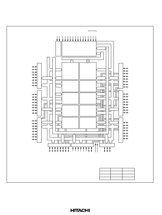
6
1.2
Block Diagram
Figure 1.1 (a) shows a block diagram of the H8/3337 Series. Figure 1.1 (b) shows a block diagram
of the H8/3397 Series.
P9
0
/
ADTRG
/
IRQ
2
/
ECS
2
P9
1
/
IRQ
1
/
EIOW
P9
2
/
IRQ
0
P9
3
/
RD
P9
4
/
WR
P9
5
/
AS
P9
6
/¯
P9
7
/
WAIT
/SDA
P3
0
/D
0
/HDB
0
P3
1
/D
1
/HDB
1
P3
2
/D
2
/HDB
2
P3
3
/D
3
/HDB
3
P3
4
/D
4
/HDB
4
P3
5
/D
5
/HDB
5
P3
6
/D
6
/HDB
6
P3
7
/D
7
/HDB
7
P8
0
/HA
0
P8
1
/GA
20
P8
2
/
CS
1
P8
3
/
IOR
P8
4
/TxD
1
/
IRQ
3
/
IOW
P8
5
/RxD
1
/
IRQ
4
/
CS
2
P8
6
/SCK
1
/
IRQ
5
/SCL
P1
0
/A
0
P1
1
/A
1
P1
2
/A
2
P1
3
/A
3
P1
4
/A
4
P1
5
/A
5
P1
6
/A
6
P1
7
/A
7
P2
0
/A
8
P2
1
/A
9
P2
2
/A
10
P2
3
/A
11
P2
4
/A
12
P2
5
/A
13
P2
6
/A
14
P2
7
/A
15
P6
0
/FTCI/
KEYIN
0
P6
1
/FTOA/
KEYIN
1
P6
2
/FTIA/
KEYIN
2
P6
3
/FTIB/
KEYIN
3
P6
4
/FTIC/
KEYIN
4
P6
5
/FTID/
KEYIN
5
P6
6
/FTOB/
IRQ
6
/
KEYIN
6
P6
7
/
IRQ
7
/
KEYIN
7
P4
0
/TMCI
0
P4
1
/TMO
0
P4
2
/TMRI
0
P4
3
/TMCI
1
/HIRQ
11
P4
4
/TMO
1
/HIRQ
1
P4
5
/TMRI
1
/HIRQ
12
P4
6
/PW
0
P4
7
/PW
1
P7
0
/AN
0
P7
1
/AN
1
P7
2
/AN
2
P7
3
/AN
3
P7
4
/AN
4
P7
5
/AN
5
P7
6
/AN
6
/DA
0
P7
7
/AN
7
/DA
1
P5
0
/TxD
0
P5
1
/RxD
0
P5
2
/SCK
0
AV
CC
AV
SS
RES
STBY
NMI
MD
0
MD
1
V
CC
V
CC
V
SS
V
SS
V
SS
V
SS
V
SS
V
SS
V
SS
XTAL
EXTAL
Port 9
Port 3
Port 8
Port 6
Port 2
Port 1
Port 4
Port 7
Port 5
Data bus (low)
RAM
H8/3337Y: 2 kbytes
H8/3336Y: 2 kbytes
H8/3334Y: 1 kbyte
10-bit
A/D converter
(8 channels)
8-bit
D/A converter
(2 channels)
16-bit
free-running
timer
8-bit timer
(2 channels)
PWM timer
(2 channels)
Clock pulse
generator
ROM
Flash memory,
PROM or mask ROM
H8/3337Y: 60 kbytes
H8/3336Y: 48 kbytes
H8/3334Y: 32 kbytes
Watchdog
timer
Host
interface
Serial communi-
cation interface
(2 channels)
I
2
C bus interface
(1 channel) (option)
CPU
H8/300
*
Data bus (high)
Address bus
Memory Sizes
ROM
60 kbytes
48 kbytes
32 kbytes
H8/3337Y
H8/3336Y
H8/3334Y
RAM
2 kbytes
2 kbytes
1 kbyte
Note:
*
In the case of the CP-84 and CG-84
Figure 1.1 (a) Block Diagram for H8/3337 Series
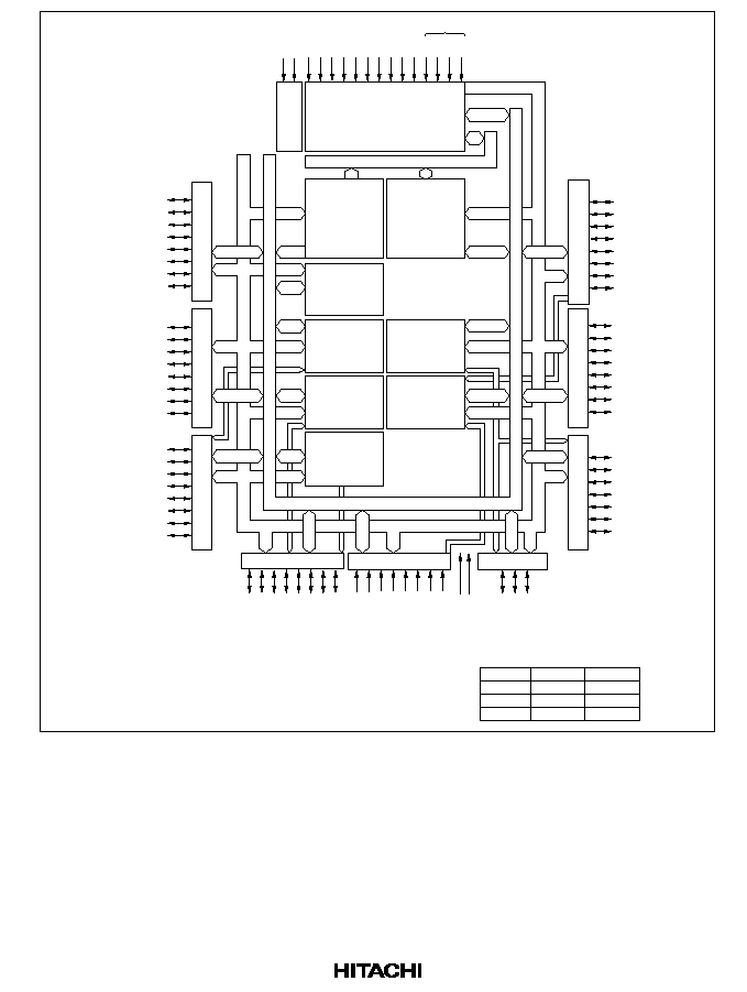
7
P9
0
/
ADTRG
/
IRQ
2
P9
1
/
IRQ
1
P9
2
/
IRQ
0
P9
3
/
RD
P9
4
/
WR
P9
5
/
AS
P9
6
/¯
P9
7
/
WAIT
P3
0
/D
0
P3
1
/D
1
P3
2
/D
2
P3
3
/D
3
P3
4
/D
4
P3
5
/D
5
P3
6
/D
6
P3
7
/D
7
P8
0
P8
1
P8
2
P8
3
P8
4
/TxD
1
/
IRQ
3
P8
5
/RxD
1
/
IRQ
4
P8
6
/SCK
1
/
IRQ
5
P1
0
/A
0
P1
1
/A
1
P1
2
/A
2
P1
3
/A
3
P1
4
/A
4
P1
5
/A
5
P1
6
/A
6
P1
7
/A
7
P2
0
/A
8
P2
1
/A
9
P2
2
/A
10
P2
3
/A
11
P2
4
/A
12
P2
5
/A
13
P2
6
/A
14
P2
7
/A
15
P6
0
/FTCI/
KEYIN
0
P6
1
/FTOA/
KEYIN
1
P6
2
/FTIA/
KEYIN
2
P6
3
/FTIB/
KEYIN
3
P6
4
/FTIC/
KEYIN
4
P6
5
/FTID/
KEYIN
5
P6
6
/FTOB/
IRQ
6
/
KEYIN
6
P6
7
/
IRQ
7
/
KEYIN
7
P4
0
/TMCI
0
P4
1
/TMO
0
P4
2
/TMRI
0
P4
3
/TMCI
1
P4
4
/TMO
1
P4
5
/TMRI
1
P4
6
/PW
0
P4
7
/PW
1
P7
0
/AN
0
P7
1
/AN
1
P7
2
/AN
2
P7
3
/AN
3
P7
4
/AN
4
P7
5
/AN
5
P7
6
/AN
6
P7
7
/AN
7
P5
0
/TxD
0
P5
1
/RxD
0
P5
2
/SCK
0
AV
CC
AV
SS
XTAL
EXTAL
Port 9
Port 3
Port 8
Port 6
Port 2
Port 1
Port 4
Port 7
Port 5
Data bus (low)
10-bit
A/D converter
(8 channels)
16-bit
free-running
timer
8-bit timer
(2 channels)
PWM timer
(2 channels)
Clock pulse
generator
Watchdog
timer
Serial
communication
interface
(2 channels)
CPU
H8/300
Data bus (high)
Address bus
RAM
H8/3397: 2 kbytes
H8/3396: 2 kbytes
H8/3394: 1 kbyte
ROM
(Mask ROM)
H8/3397: 60 kbytes
H8/3396: 48 kbytes
H8/3394: 32 kbytes
RES
STBY
NMI
MD
0
MD
1
V
CC
V
CC
V
SS
V
SS
V
SS
V
SS
V
SS
V
SS
V
SS
*
Memory Sizes
ROM
60 kbytes
48 kbytes
32 kbytes
H8/3397
H8/3396
H8/3394
RAM
2 kbytes
2 kbytes
1 kbyte
Note:
*
In the case of the CP-84 and CG-84
Figure 1.1 (b) Block Diagram for H8/3397 Series

8
1.3Pin Assignments and Functions
1.3.1
Pin Arrangement
Figure 1.2 (a) shows the pin arrangement of the FP-80A and TFP-80C packages for the H8/3337
Series, and figure 1.2 (b) shows the packages for the H8/3397 Series.
Figure 1.3 (a) shows the pin arrangement of the CP-84 and CG-84 packages for the H8/3337
Series, and figure 1.3 (b) shows the packages for the H8/3397 Series.
P1
4
/A
4
P1
5
/A
5
P1
6
/A
6
P1
7
/A
7
V
SS
P2
0
/A
8
P2
1
/A
9
P2
2
/A
10
P2
3
/A
11
P2
4
/A
12
P2
5
/A
13
P2
6
/A
14
P2
7
/A
15
V
CC
P4
7
/PW
1
P4
6
/PW
0
P4
5
/TMRI
1
/HIRQ
12
P4
4
/TMO
1
/HIRQ
1
P4
3
/TMCI
1
/HIRQ
11
P4
2
/TMRI
0
RES
XTAL
EXTAL
MD
1
MD
0
NMI
STBY
/FV
PP
*
V
CC
SCK
0
/P5
2
RxD
0
/P5
1
TxD
0
/P5
0
V
SS
WAIT
/SDA/P9
7
¯/P9
6
AS
/P9
5
WR
/P9
4
RD
/P9
3
IRQ
0
/P9
2
EIOW
/
IRQ
1
/P9
1
ADTRG
/
ECS
2
/
IRQ
2
/P9
0
1
2
3
4
5
6
7
8
9
10
11
12
13
14
15
16
17
18
19
20
61
62
63
64
65
66
67
68
69
70
71
72
73
74
75
76
77
78
79
80
A
3
/
P1
3
A
2
/
P1
2
A
1
/
P1
1
A
0
/
P1
0
D
0
/
HDB
0
/
P3
0
D
1
/
HDB
1
/
P3
1
D
2
/
HDB
2
/
P3
2
D
3
/
HDB
3
/
P3
3
D
4
/
HDB
4
/
P3
4
D
5
/
HDB
5
/
P3
5
D
6
/
HDB
6
/
P3
6
D
7
/
HDB
7
/
P3
7
V
SS
HA
0
/
P8
0
GA
20
/
P8
1
CS
1
/
P8
2
IOR
/
P8
3
TxD
1
/
IRQ
3
/
IOW
/
P8
4
RxD
1
/
IRQ
4
/
CS
2
/
P8
5
SCL
/
SCK
1
/
IRQ
5
/
P8
6
40
39
38
37
36
35
34
33
32
31
30
29
28
27
26
25
24
23
22
21
P4
1
/
TMO
0
P4
0
/
TMCI
0
AV
SS
P7
7
/
AN
7
/DA
1
P7
6
/
AN
6
/DA
0
P7
5
/
AN
5
P7
4
/
AN
4
P7
3
/
AN
3
P7
2
/
AN
2
P7
1
/
AN
1
P7
0
/
AN
0
AV
CC
P6
7
/
KEYIN
7
/
IRQ
7
P6
6
/
FTOB
/
KEYIN
6
/
IRQ
6
P6
5
/
FTID/
KEYIN
5
P6
4
/
FTIC/
KEYIN
4
P6
3
/
FTIB
/
KEYIN
3
P6
2
/
FTIA
/
KEYIN
2
P6
1
/
FTOA
/
KEYIN
1
P6
0
/
FTCI
/
KEYIN
0
60
59
58
57
56
55
54
53
52
51
50
49
48
47
46
45
44
43
42
41
H8/3337 Series
FP-80A, TFP-80C
(top view)
Note:
*
In the S-mask model (single-power-supply model), pin 7 functions only as the
STBY
pin.
Figure 1.2 (a) Pin Arrangement for H8/3337 Series (FP-80A, TFP-80C, Top View)
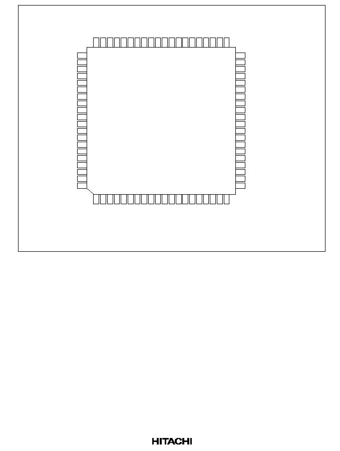
9
P1
4
/A
4
P1
5
/A
5
P1
6
/A
6
P1
7
/A
7
V
SS
P2
0
/A
8
P2
1
/A
9
P2
2
/A
10
P2
3
/A
11
P2
4
/A
12
P2
5
/A
13
P2
6
/A
14
P2
7
/A
15
V
CC
P4
7
/PW
1
P4
6
/PW
0
P4
5
/TMRI
1
P4
4
/TMO
1
P4
3
/TMCI
1
P4
2
/TMRI
0
RES
XTAL
EXTAL
MD
1
MD
0
NMI
STBY
V
CC
SCK
0
/P5
2
RxD
0
/P5
1
TxD
0
/P5
0
V
SS
WAIT
/P9
7
¯/P9
6
AS
/P9
5
WR
/P9
4
RD
/P9
3
IRQ
0
/P9
2
IRQ
1
/P9
1
A
DTRG
/
IRQ
2
/P9
0
1
2
3
4
5
6
7
8
9
10
11
12
13
14
15
16
17
18
19
20
61
62
63
64
65
66
67
68
69
70
71
72
73
74
75
76
77
78
79
80
A
3
/
P1
3
A
2
/
P1
2
A
1
/
P1
1
A
0
/
P1
0
D
0
/
P3
0
D
1
/
P3
1
D
2
/
P3
2
D
3
/
P3
3
D
4
/
P3
4
D
5
/
P3
5
D
6
/
P3
6
D
7
/
P3
7
V
SS
P8
0
P8
1
P8
2
P8
3
TxD
1
/
IRQ
3
/
P8
4
RxD
1
/
IRQ
4
/
P8
5
SCK
1
/
IRQ
5
/
P8
6
40
39
38
37
36
35
34
33
32
31
30
29
28
27
26
25
24
23
22
21
P4
1
/
TMO
0
P4
0
/
TMCI
0
AV
SS
P7
7
/
AN
7
P7
6
/
AN
6
P7
5
/
AN
5
P7
4
/
AN
4
P7
3
/
AN
3
P7
2
/
AN
2
P7
1
/
AN
1
P7
0
/
AN
0
AV
CC
P6
7
/
KEYIN
7
/
IRQ
7
P6
6
/
FTOB
/
KEYIN
6
/
IRQ
6
P6
5
/
FTID
/
KEYIN
5
P6
4
/
FTIC
/
KEYIN
4
P6
3
/
FTIB
/
KEYIN
3
P6
2
/
FTIA
/
KEYIN
2
P6
1
/
FTOA
/
KEYIN
1
P6
0
/
FTCI
/
KEYIN
0
60
59
58
57
56
55
54
53
52
51
50
49
48
47
46
45
44
43
42
41
H8/3397 Series
FP-80A, TFP-80C
(top view)
Figure 1.2 (b) Pin Arrangement for H8/3397 Series (FP-80A, TFP-80C, Top View)
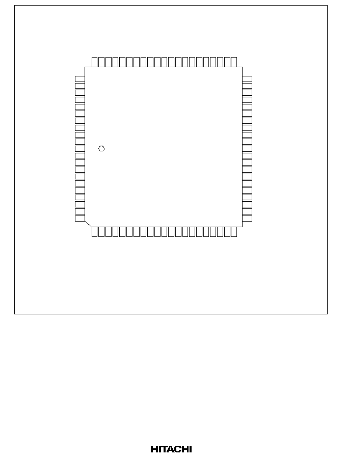
10
P1
4
/A
4
P1
5
/A
5
P1
6
/A
6
P1
7
/A
7
V
SS
P2
0
/A
8
P2
1
/A
9
P2
2
/A
10
P2
3
/A
11
P2
4
/A
12
V
SS
P2
5
/A
13
P2
6
/A
14
P2
7
/A
15
V
CC
P4
7
/PW
1
P4
6
/PW
0
P4
5
/TMRI
1
/HIRQ
12
P4
4
/TMO
1
/HIRQ
1
P4
3
/TMCI
1
/HIRQ
11
P4
2
/TMRI
0
RES
XTAL
EXTAL
MD
1
MD
0
NMI
STBY
/FV
PP
*
V
CC
SCK
0
/P5
2
RxD
0
/P5
1
TxD
0
/P5
0
V
SS
V
SS
WAIT
/SDA/P9
7
¯/P9
6
AS
/P9
5
WR
/P9
4
RD
/P9
3
IRQ
0
/P9
2
EIOW
/
IRQ
1
/P9
1
ADTRG
/
ECS
2
/
IRQ
2
/P9
0
12
13
14
15
16
17
18
19
20
21
22
23
24
25
26
27
28
29
30
31
32
75
76
77
78
79
80
81
82
83
84
1
2
3
4
5
6
7
8
9
10
11
A
3
/
P1
3
A
2
/
P1
2
A
1
/
P1
1
A
0
/
P1
0
D
0
/
HDB
0
/
P3
0
D
1
/
HDB
1
/
P3
1
D
2
/
HDB
2
/
P3
2
D
3
/
HDB
3
/
P3
3
D
4
/
HDB
4
/
P3
4
D
5
/
HDB
5
/
P3
5
D
6
/
HDB
6
/
P3
6
V
SS
D
7
/
HDB
7
/
P3
7
V
SS
HA
0
/
P8
0
GA
20
/
P8
1
CS
1
/
P8
2
IOR
/
P8
3
TxD
1
/
IRQ
3
/
IOW
/P8
4
RxD
1
/
IRQ
4
/
CS
2
/
P8
5
SCL
/
SCK
1
/
IRQ
5
/
P8
6
53
52
51
50
49
48
47
46
45
44
43
42
41
40
39
38
37
36
35
34
33
P4
1
/
TMO
0
P4
0
/
TMCI
0
AV
SS
P7
7
/
AN
7
/DA
1
P7
6
/
AN
6
/DA
0
P7
5
/
AN
5
P7
4
/
AN
4
P7
3
/
AN
3
P7
2
/
AN
2
P7
1
/
AN
1
P7
0
/
AN
0
AV
CC
V
SS
P6
7
/
KEYIN
7
/
IRQ
7
P6
6
/
FTOB
/
KEYIN
6
/
IRQ
6
P6
5
/
FTID
/
KEYIN
5
P6
4
/
FTIC
/
KEYIN
4
P6
3
/
FTIB
/
KEYIN
3
P6
2
/
FTIA
/
KEYIN
2
P6
1
/
FTOA
/
KEYIN
1
P6
0
/
FTCI
/
KEYIN
0
74
73
72
71
70
69
68
67
66
65
64
63
62
61
60
59
58
57
56
55
54
H8/3337 Series
CP-84, CG-84
(top view)
Note:
*
In the S-mask model (single-power-supply model), pin 18 functions only as the
STBY
pin.
Figure 1.3 (a) Pin Arrangement for H8/3337 Series (CP-84, CG-84, Top View)
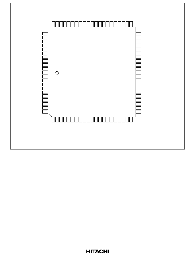
11
P1
4
/A
4
P1
5
/A
5
P1
6
/A
6
P1
7
/A
7
V
SS
P2
0
/A
8
P2
1
/A
9
P2
2
/A
10
P2
3
/A
11
P2
4
/A
12
V
SS
P2
5
/A
13
P2
6
/A
14
P2
7
/A
15
V
CC
P4
7
/PW
1
P4
6
/PW
0
P4
5
/TMRI
1
P4
4
/TMO
1
P4
3
/TMCI
1
P4
2
/TMRI
0
RES
XTAL
EXTAL
MD
1
MD
0
NMI
STBY
V
CC
SCK
0
/P5
2
RxD
0
/P5
1
TxD
0
/P5
0
V
SS
V
SS
WAIT
/P9
7
¯/P9
6
AS
/P9
5
WR
/P9
4
RD
/P9
3
IRQ
0
/P9
2
IRQ
1
/P9
1
A
DTRG
/
IRQ
2
/P9
0
12
13
14
15
16
17
18
19
20
21
22
23
24
25
26
27
28
29
30
31
32
74
73
72
71
70
69
68
67
66
65
64
63
62
61
60
59
58
57
56
55
54
75
76
77
78
79
80
81
82
83
84
1
2
3
4
5
6
7
8
9
10
11
53
52
51
50
49
48
47
46
45
44
43
42
41
40
39
38
37
36
35
34
33
P4
1
/
TMO
0
P4
0
/
TMCI
0
AV
SS
P7
7
/
AN
7
P7
6
/
AN
6
P7
5
/
AN
5
P7
4
/
AN
4
P7
3
/
AN
3
P7
2
/
AN
2
P7
1
/
AN
1
P7
0
/
AN
0
AV
CC
V
SS
P6
7
/
KEYIN
7
/
IRQ
7
P6
6
/
FTOB
/
KEYIN
6
/
IRQ
6
P6
5
/
FTID
/
KEYIN
5
P6
4
/
FTIC
/
KEYIN
4
P6
3
/
FTIB
/
KEYIN
3
P6
2
/
FTIA
/
KEYIN
2
P6
1
/
FTOA
/
KEYIN
1
P6
0
/
FTCI
/
KEYIN
0
A
3
/P1
3
A
2
/P1
2
A
1
/P1
1
A
0
/P1
0
D
0
/P3
0
D
1
/P3
1
D
2
/P3
2
D
3
/P3
3
D
4
/P3
4
D
5
/P3
5
D
6
/P3
6
V
SS
D
7
/P3
7
V
SS
P8
0
P8
1
P8
2
P8
3
TxD
1
/
IRQ
3
/P8
4
RxD
1
/
IRQ
4
/P8
5
SCK
1
/
IRQ
5
/P8
6
H8/3397 Series
CP-84
(top view)
Figure 1.3 (b) Pin Arrangement for H8/3397 Series (CP-84, Top View)

12
1.3.2
Pin Functions
Pin Assignments in Each Operating Mode: Table 1.2 (a) and table 1.2 (b) lists the assignments
of the pins of the FP-80A, TFP-80, CP-84, and CG-84 packages in each operating mode.
Table 1.2 (a) Pin Assignments for H8/3337 Series in Each Operating Mode
Pin No.
Expanded Modes
Single-Chip Mode
Flash
Mode 3
EPROM Memory
FP-80A,
TFP-80C
CP-84,
CG-84
Mode 1
Mode 2
HIF
Disabled
HIF
Enabled
Writer
Mode
Writer
Mode
1
12
RES
RES
RES
RES
V
PP
RES
2
13
XTAL
XTAL
XTAL
XTAL
NC
XTAL
3
14
EXTAL
EXTAL
EXTAL
EXTAL
NC
EXTAL
4
15
MD
1
MD
1
MD
1
MD
1
V
SS
V
SS
5
16
MD
0
MD
0
MD
0
MD
0
V
SS
V
SS
6
17
NMI
NMI
NMI
NMI
EA
9
FA
9
7
18
STBY
STBY
/FV
PP
STBY
/FV
PP
STBY
/FV
PP
V
SS
FV
PP
8
19
V
CC
V
CC
V
CC
V
CC
V
CC
V
CC
9
20
P5
2
/SCK
0
P5
2
/SCK
0
P5
2
/SCK
0
P5
2
/SCK
0
NC
NC
10
21
P5
1
/RxD
0
P5
1
/RxD
0
P5
1
/RxD
0
P5
1
/RxD
0
NC
NC
11
22
P5
0
/TxD
0
P5
0
/TxD
0
P5
0
/TxD
0
P5
0
/TxD
0
NC
NC
12
23
V
SS
V
SS
V
SS
V
SS
V
SS
V
SS
--
24
V
SS
V
SS
V
SS
V
SS
V
SS
V
SS
13
25
P9
7
/
WAIT
/SDA P9
7
/
WAIT
/SDA P9
7
/SDA
P9
7
/SDA
NC
V
CC
14
26
¯
¯
P9
6
/¯
P9
6
/¯
NC
NC
15
27
AS
AS
P9
5
P9
5
NC
FA
16
16
28
WR
WR
P9
4
P9
4
NC
FA
15
17
29
RD
RD
P9
3
P9
3
NC
WE
18
30
P9
2
/
IRQ
0
P9
2
/
IRQ
0
P9
2
/
IRQ
0
P9
2
/
IRQ
0
PGM
V
SS
19
31
P9
1
/
IRQ
1
when HIF is disabled or STAC bit is 0 in STCR;
EIOW
/
IRQ
1
when HIF is enabled and STAC bit is 1
EA
15
V
CC
20
32
P9
0
/
IRQ
2
/
ADTRG
when HIF is disabled or STAC bit is 0 in
STCR;
ECS
2
/
IRQ
2
when HIF is enabled and STAC bit is 1
EA
16
V
CC
21
33
P6
0
/FTCI/
KEYIN
0
P6
0
/FTCI/
KEYIN
0
P6
0
/FTCI/
KEYIN
0
P6
0
/FTCI/
KEYIN
0
NC
NC

13
Pin No.
Expanded Modes
Single-Chip Mode
Flash
Mode 3
EPROM Memory
FP-80A,
TFP-80C
CP-84,
CG-84
Mode 1
Mode 2
HIF
Disabled
HIF
Enabled
Writer
Mode
Writer
Mode
22
34
P6
1
/FTOA/
KEYIN
1
P6
1
/FTOA/
KEYIN
1
P6
1
/FTOA/
KEYIN
1
P6
1
/FTOA/
KEYIN
1
NC
NC
23
35
P6
2
/FTIA/
KEYIN
2
P6
2
/FTIA/
KEYIN
2
P6
2
/FTIA/
KEYIN
2
P6
2
/FTIA/
KEYIN
2
NC
NC
24
36
P6
3
/FTIB/
KEYIN
3
P6
3
/FTIB/
KEYIN
3
P6
3
/FTIB/
KEYIN
3
P6
3
/FTIB/
KEYIN
3
V
CC
V
CC
25
37
P6
4
/FTIC/
KEYIN
4
P6
4
/FTIC/
KEYIN
4
P6
4
/FTIC/
KEYIN
4
P6
4
/FTIC/
KEYIN
4
V
CC
V
CC
26
38
P6
5
/FTID/
KEYIN
5
P6
5
/FTID/
KEYIN
5
P6
5
/FTID/
KEYIN
5
P6
5
/FTID/
KEYIN
5
NC
NC
27
39
P6
6
/FTOB/
IRQ
6
/
KEYIN
6
P6
6
/FTOB/
IRQ
6
/
KEYIN
6
P6
6
/FTOB/
IRQ
6
/
KEYIN
6
P6
6
/FTOB/
IRQ
6
/
KEYIN
6
NC
NC
28
40
P6
7
/
IRQ
7
/
KEYIN
7
P6
7
/
IRQ
7
/
KEYIN
7
P6
7
/
IRQ
7
/
KEYIN
7
P6
7
/
IRQ
7
/
KEYIN
7
NC
V
SS
--
41
V
SS
V
SS
V
SS
V
SS
V
SS
V
SS
29
42
AV
CC
AV
CC
AV
CC
AV
CC
V
CC
V
CC
30
43
P7
0
/AN
0
P7
0
/AN
0
P7
0
/AN
0
P7
0
/AN
0
NC
NC
31
44
P7
1
/AN
1
P7
1
/AN
1
P7
1
/AN
1
P7
1
/AN
1
NC
NC
32
45
P7
2
/AN
2
P7
2
/AN
2
P7
2
/AN
2
P7
2
/AN
2
NC
NC
33
46
P7
3
/AN
3
P7
3
/AN
3
P7
3
/AN
3
P7
3
/AN
3
NC
NC
34
47
P7
4
/AN
4
P7
4
/AN
4
P7
4
/AN
4
P7
4
/AN
4
NC
NC
35
48
P7
5
/AN
5
P7
5
/AN
5
P7
5
/AN
5
P7
5
/AN
5
NC
NC
36
49
P7
6
/AN
6
/DA
0
P7
6
/AN
6
/DA
0
P7
6
/AN
6
/DA
0
P7
6
/AN
6
/DA
0
NC
NC
37
50
P7
7
/AN
7
/DA
1
P7
7
/AN
7
/DA
1
P7
7
/AN
7
/DA
1
P7
7
/AN
7
/DA
1
NC
NC
38
51
AV
SS
AV
SS
AV
SS
AV
SS
V
SS
V
SS
39
52
P4
0
/TMCI
0
P4
0
/TMCI
0
P4
0
/TMCI
0
P4
0
/TMCI
0
NC
NC
40
53
P4
1
/TMO
0
P4
1
/TMO
0
P4
1
/TMO
0
P4
1
/TMO
0
NC
NC
41
54
P4
2
/TMRI
0
P4
2
/TMRI
0
P4
2
/TMRI
0
P4
2
/TMRI
0
NC
NC
42
55
P4
3
/TMCI
1
/
HIRQ
11
*
P4
3
/TMCI
1
/
HIRQ
11
*
P4
3
/TMCI
1
HIRQ
11
/
TMCI
1
NC
NC

14
Pin No.
Expanded Modes
Single-Chip Mode
Flash
Mode 3
EPROM Memory
FP-80A,
TFP-80C
CP-84,
CG-84
Mode 1
Mode 2
HIF
Disabled
HIF
Enabled
Writer
Mode
Writer
Mode
43
56
P4
4
/TMO
1
/
HIRQ
1
*
P4
4
/TMO
1
/
HIRQ
1
*
P4
4
/TMO
1
HIRQ
1
/TMO
1
NC
NC
44
57
P4
5
/TMRI
1
/
HIRQ
12
*
P4
5
/TMRI
1
/
HIRQ
12
*
P4
5
/TMRI
1
HIRQ
12
/
TMRI
1
NC
NC
45
58
P4
6
/PW
0
P4
6
/PW
0
P4
6
/PW
0
P4
6
/PW
0
NC
NC
46
59
P4
7
/PW
1
P4
7
/PW
1
P4
7
/PW
1
P4
7
/PW
1
NC
NC
47
60
V
CC
V
CC
V
CC
V
CC
V
CC
V
CC
48
61
A
15
P2
7
/A
15
P2
7
P2
7
CE
CE
49
62
A
14
P2
6
/A
14
P2
6
P2
6
EA
14
FA
14
50
63
A
13
P2
5
/A
13
P2
5
P2
5
EA
13
FA
13
--
64
V
SS
V
SS
V
SS
V
SS
V
SS
V
SS
51
65
A
12
P2
4
/A
12
P2
4
P2
4
EA
12
FA
12
52
66
A
11
P2
3
/A
11
P2
3
P2
3
EA
11
FA
11
53
67
A
10
P2
2
/A
10
P2
2
P2
2
EA
10
FA
10
54
68
A
9
P2
1
/A
9
P2
1
P2
1
OE
OE
55
69
A
8
P2
0
/A
8
P2
0
P2
0
EA
8
FA
8
56
70
V
SS
V
SS
V
SS
V
SS
V
SS
V
SS
57
71
A
7
P1
7
/A
7
P1
7
P1
7
EA
7
FA
7
58
72
A
6
P1
6
/A
6
P1
6
P1
6
EA
6
FA
6
59
73
A
5
P1
5
/A
5
P1
5
P1
5
EA
5
FA
5
60
74
A
4
P1
4
/A
4
P1
4
P1
4
EA
4
FA
4
61
75
A
3
P1
3
/A
3
P1
3
P1
3
EA
3
FA
3
62
76
A
2
P1
2
/A
2
P1
2
P1
2
EA
2
FA
2
63
77
A
1
P1
1
/A
1
P1
1
P1
1
EA
1
FA
1
64
78
A
0
P1
0
/A
0
P1
0
P1
0
EA
0
FA
0
65
79
D
0
D
0
P3
0
HDB
0
EO
0
FO
0
66
80
D
1
D
1
P3
1
HDB
1
EO
1
FO
1
67
81
D
2
D
2
P3
2
HDB
2
EO
2
FO
2
68
82
D
3
D
3
P3
3
HDB
3
EO
3
FO
3

15
Pin No.
Expanded Modes
Single-Chip Mode
Flash
Mode 3
EPROM Memory
FP-80A,
TFP-80C
CP-84,
CG-84
Mode 1
Mode 2
HIF
Disabled
HIF
Enabled
Writer
Mode
Writer
Mode
69
83
D
4
D
4
P3
4
HDB
4
EO
4
FO
4
70
84
D
5
D
5
P3
5
HDB
5
EO
5
FO
5
71
1
D
6
D
6
P3
6
HDB
6
EO
6
FO
6
--
2
V
SS
V
SS
V
SS
V
SS
V
SS
V
SS
72
3
D
7
D
7
P3
7
HDB
7
EO
7
FO
7
73
4
V
SS
V
SS
V
SS
V
SS
V
SS
V
SS
74
5
P8
0
/HA
0
*
P8
0
/HA
0
*
P8
0
HA
0
NC
NC
75
6
P8
1
/GA
20
*
P8
1
/GA
20
*
P8
1
P8
1
/GA
20
NC
NC
76
7
P8
2
/CS
1
*
P8
2
/CS
1
*
P8
2
CS
1
NC
NC
77
8
P8
3
/
IOR*
P8
3
/
IOR*
P8
3
IOR
NC
NC
78
9
P8
4
/
IRQ
3
/TxD
1
when HIF is disabled or STAC bit is 1 in
STCR;
IOW
/
IRQ
3
when HIF is enabled and STAC bit is 0
NC
NC
79
10
P8
5
/
IRQ
4
/RxD
1
when HIF is disabled or STAC bit is 1 in
STCR;
CS
2
/
IRQ
4
when HIF is enabled and STAC bit is 0
NC
NC
80
11
P8
6
/SCK
1
/
IRQ
5
/SCL
P8
6
/SCK
1
/
IRQ
5
/SCL
P8
6
/SCK
1
/
IRQ
5
/SCL
P8
6
/SCK
1
/
IRQ
5
/SCL
NC
NC
Notes: 1. Pins marked NC should be left unconnected.
2. For details on witer mode, refer to 18.2, Writer Mode, 19.6 Flash Memory Writer Mode
(H8/3334YF), 20.6 Flash Memory Writer Mode (H8/3337YF) and 21.5, Flash Memory
Writer Mode (H8/3337SF).
3. In this chip, except for the S-mask model (single-power-supply specification), the same
pin is used for STBY and FV
PP
. When this pin is driven low, a transition is made to
hardware standby mode. This happens not only in the normal operating modes (modes
1, 2, and 3), but also when programming the flash memory with a PROM writer. When
using a PROM programmer to program dual-power-supply flash memory, therefore, the
PROM programmer specifications should provide for this pin to be held at the V
CC
level
except when programming (FV
PP
= 12 V).
*
Differs as in mode 3, depending on whether the host interface is enabled or disabled.

16
Table 1.2 (b) Pin Assignments for H8/3397 Series in Each Operating Mode
Pin No.
Expanded Modes
Single-Chip Mode
FP-80A,
TFP-80C
CP-84,
CG-84
Mode 1
Mode 2
Mode 3
1
12
RES
RES
RES
2
13
XTAL
XTAL
XTAL
3
14
EXTAL
EXTAL
EXTAL
4
15
MD
1
MD
1
MD
1
5
16
MD
0
MD
0
MD
0
6
17
NMI
NMI
NMI
7
18
STBY
STBY
STBY
8
19
V
CC
V
CC
V
CC
9
20
P5
2
/SCK
0
P5
2
/SCK
0
P5
2
/SCK
0
10
21
P5
1
/RxD
0
P5
1
/RxD
0
P5
1
/RxD
0
11
22
P5
0
/TxD
0
P5
0
/TxD
0
P5
0
/TxD
0
12
23
V
SS
V
SS
V
SS
--
24
V
SS
V
SS
V
SS
13
25
P9
7
/
WAIT
P9
7
/
WAIT
P9
7
14
26
¯
¯
P9
6
/¯
15
27
AS
AS
P9
5
16
28
WR
WR
P9
4
17
29
RD
RD
P9
3
18
30
P9
2
/
IRQ
0
P9
2
/
IRQ
0
P9
2
/
IRQ
0
19
31
P9
1
/
IRQ
1
P9
1
/
IRQ
1
P9
1
/
IRQ
1
20
32
P9
0
/
IRQ
2
/
ADTRG
P9
0
/
IRQ
2
/
ADTRG
P9
0
/
IRQ
2
/
ADTRG
21
33
P6
0
/FTCI/
KEYIN
0
P6
0
/FTCI/
KEYIN
0
P6
0
/FTCI/
KEYIN
0
22
34
P6
1
/FTOA/
KEYIN
1
P6
1
/FTOA/
KEYIN
1
P6
1
/FTOA/
KEYIN
1
23
35
P6
2
/FTIA/
KEYIN
2
P6
2
/FTIA/
KEYIN
2
P6
2
/FTIA/
KEYIN
2
24
36
P6
3
/FTIB/
KEYIN
3
P6
3
/FTIB/
KEYIN
3
P6
3
/FTIB/
KEYIN
3
25
37
P6
4
/FTIC/
KEYIN
4
P6
4
/FTIC/
KEYIN
4
P6
4
/FTIC/
KEYIN
4
26
38
P6
5
/FTID/
KEYIN
5
P6
5
/FTID/
KEYIN
5
P6
5
/FTID/
KEYIN
5
27
39
P6
6
/FTOB/
IRQ
6
/
KEYIN
6
P6
6
/FTOB/
IRQ
6
/
KEYIN
6
P6
6
/FTOB/
IRQ
6
/
KEYIN
6

17
Pin No.
Expanded Modes
Single-Chip Mode
FP-80A,
TFP-80C
CP-84,
CG-84
Mode 1
Mode 2
Mode 3
28
40
P6
7
/
IRQ
7
/
KEYIN
7
P6
7
/
IRQ
7
/
KEYIN
7
P6
7
/
IRQ
7
/
KEYIN
7
--
41
V
SS
V
SS
V
SS
29
42
AV
CC
AV
CC
AV
CC
30
43
P7
0
/AN
0
P7
0
/AN
0
P7
0
/AN
0
31
44
P7
1
/AN
1
P7
1
/AN
1
P7
1
/AN
1
32
45
P7
2
/AN
2
P7
2
/AN
2
P7
2
/AN
2
33
46
P7
3
/AN
3
P7
3
/AN
3
P7
3
/AN
3
34
47
P7
4
/AN
4
P7
4
/AN
4
P7
4
/AN
4
35
48
P7
5
/AN
5
P7
5
/AN
5
P7
5
/AN
5
36
49
P7
6
/AN
6
P7
6
/AN
6
P7
6
/AN
6
37
50
P7
7
/AN
7
P7
7
/AN
7
P7
7
/AN
7
38
51
AV
SS
AV
SS
AV
SS
39
52
P4
0
/TMCI
0
P4
0
/TMCI
0
P4
0
/TMCI
0
40
53
P4
1
/TMO
0
P4
1
/TMO
0
P4
1
/TMO
0
41
54
P4
2
/TMRI
0
P4
2
/TMRI
0
P4
2
/TMRI
0
42
55
P4
3
/TMCI
1
P4
3
/TMCI
1
P4
3
/TMCI
1
43
56
P4
4
/TMO
1
P4
4
/TMO
1
P4
4
/TMO
1
44
57
P4
5
/TMRI
1
P4
5
/TMRI
1
P4
5
/TMRI
1
45
58
P4
6
/PW
0
P4
6
/PW
0
P4
6
/PW
0
46
59
P4
7
/PW
1
P4
7
/PW
1
P4
7
/PW
1
47
60
V
CC
V
CC
V
CC
48
61
A
15
P2
7
/A
15
P2
7
49
62
A
14
P2
6
/A
14
P2
6
50
63
A
13
P2
5
/A
13
P2
5
--
64
V
SS
V
SS
V
SS
51
65
A
12
P2
4
/A
12
P2
4
52
66
A
11
P2
3
/A
11
P2
3
53
67
A
10
P2
2
/A
10
P2
2
54
68
A
9
P2
1
/A
9
P2
1

18
Pin No.
Expanded Modes
Single-Chip Mode
FP-80A,
TFP-80C
CP-84,
CG-84
Mode 1
Mode 2
Mode 3
55
69
A
8
P2
0
/A
8
P2
0
56
70
V
SS
V
SS
V
SS
57
71
A
7
P1
7
/A
7
P1
7
58
72
A
6
P1
6
/A
6
P1
6
59
73
A
5
P1
5
/A
5
P1
5
60
74
A
4
P1
4
/A
4
P1
4
61
75
A
3
P1
3
/A
3
P1
3
62
76
A
2
P1
2
/A
2
P1
2
63
77
A
1
P1
1
/A
1
P1
1
64
78
A
0
P1
0
/A
0
P1
0
65
79
D
0
D
0
P3
0
66
80
D
1
D
1
P3
1
67
81
D
2
D
2
P3
2
68
82
D
3
D
3
P3
3
69
83
D
4
D
4
P3
4
70
84
D
5
D
5
P3
5
71
1
D
6
D
6
P3
6
--
2
V
SS
V
SS
V
SS
72
3
D
7
D
7
P3
7
73
4
V
SS
V
SS
V
SS
74
5
P8
0
P8
0
P8
0
75
6
P8
1
P8
1
P8
1
76
7
P8
2
P8
2
P8
2
77
8
P8
3
P8
3
P8
3
78
9
P8
4
/
IRQ
3
/TxD
1
P8
4
/
IRQ
3
/TxD
1
P8
4
/
IRQ
3
/TxD
1
79
10
P8
5
/
IRQ
4
/RxD
1
P8
5
/
IRQ
4
/RxD
1
P8
5
/
IRQ
4
/RxD
1
80
11
P8
6
/
IRQ
5
/SCK
1
P8
6
/
IRQ
5
/SCK
1
P8
6
/
IRQ
5
/SCK
1

19
Pin Functions: Table 1.3 gives a concise description of the function of each pin.
Table 1.3Pin Functions
Pin No.
Type
Symbol
FP-80A,
TFP-80C
CP-84,
CG-84
I/O
Name and Function
Power
V
CC
8, 47
19, 60
I
Power: Connected to the power
supply.
Connect both V
CC
pins to the system
power supply.
V
SS
12, 56,
73
2, 4, 23,
24, 41,
64, 70
I
Ground: Connected to ground (0 V).
Connect all V
SS
pins to system ground
(0 V).
Clock
XTAL
2
13
I
Crystal: Connected to a crystal
oscillator. The crystal frequency should
be the same as the desired system
clock frequency. If an external clock is
input at the EXTAL pin, a reverse-
phase clock should be input at the
XTAL pin.
EXTAL
3
14
I
External crystal: Connected to a
crystal oscillator or external clock. The
frequency of the external clock should
be the same as the desired system
clock frequency. See section 6.2,
Oscillator Circuit, for examples of
connections to a crystal and external
clock.
¯
14
26
O
System clock: Supplies the system
clock to peripheral devices.
System control
RES
1
12
I
Reset: A low input causes the chip to
reset.
STBY
7
18
I
Standby: A transition to the hardware
standby mode (a power-down state)
occurs when a low input is received at
the
STBY
pin.
Address bus
A
15
to A
0
48 to 55,
57 to 64
61 to 63,
65 to 69,
71 to 78
O
Address bus: Address output pins.
Data bus
D
7
to D
0
72 to 65
3, 1,
84 to 79
I/O
Data bus: 8-bit bidirectional data bus.

20
Pin No.
Type
Symbol
FP-80A,
TFP-80C
CP-84,
CG-84
I/O
Name and Function
Bus control
WAIT
13
25
I
Wait: Requests the CPU to insert wait
states into the bus cycle when an
external address is accessed.
RD
17
29
O
Read: Goes low to indicate that the
CPU is reading an external address.
WR
16
28
O
Write: Goes low to indicate that the
CPU is writing to an external address.
AS
15
27
O
Address strobe: Goes low to indicate
that there is a valid address on the
address bus.
Interrupt signals
NMI
6
17
I
Nonmaskable interrupt: Highest-
priority interrupt request. The NMIEG
bit in the system control register
(SYSCR) determines whether the
interrupt is recognized at the rising or
falling edge of the NMI input.
IRQ
0
to
IRQ
7
18 to 20,
78 to 80,
27, 28
30 to 32,
9 to 11,
39, 40
I
Interrupt request 0 to 7: Maskable
interrupt request pins.
Operating control MD
1
MD
0
4,
5
15,
16
I
Mode: Input pins for setting the MCU
mode operating mode according to the
table below.
MD
1
MD
0
Mode
Description
0
0
Mode 0
Illegal setting
*
0
1
Mode 1
Expanded mode
with on-chip ROM
disabled
1
0
Mode 2
Expanded mode
with on-chip ROM
enabled
1
1
Mode 3
Single-chip mode
Note:
*
In the H8/3337SF (S-mask model,
single-power-supply on-chip flash
memory version), the settings MD
1
= MD
0
= 0 are used when boot
mode is set. For details, see
section 21.3, On-Board
Programming Modes.
Do not change the mode pin settings while
the chip is operating.

21
Pin No.
Type
Symbol
FP-80A,
TFP-80C
CP-84,
CG-84
I/O
Name and Function
16-bit free-
running timer
(FRT)
FTOA
FTOB
22
27
34
39
O
FRT output compare A and B:
Output pins controlled by comparators
A and B of the free-running timer.
FTCI
21
33
I
FRT counter clock input: Input pin for
an external clock signal for the free-
running timer.
FTIA to
FTID
23 to 26
35 to 38
I
FRT input capture A to D: Input
capture pins for the free-running timer.
8-bit timer
TMO
0
TMO
1
40
43
53
56
O
8-bit timer output (channels 0 and
1): Compare-match output pins for the
8-bit timers.
TMCI
0
TMCI
1
39
42
52
55
I
8-bit timer counter clock input
(channels 0 and 1): External clock
input pins for the 8-bit timer counters.
TMRI
0
TMRI
1
41
44
54
57
I
8-bit timer counter reset input
(channels 0 and 1): A high input at
these pins resets the 8-bit timer
counters.
PWM timer
PW
0
PW
1
45
46
58
59
O
PWM timer output (channels 0 and
1): Pulse-width modulation timer
output pins.
Serial communi-
cation interface
(SCI)
TxD
0
TxD
1
11
78
22
9
O
Transmit data (channels 0 and 1):
Data output pins for the serial
communication interface.
RxD
0
RxD
1
10
79
21
10
I
Receive data (channels 0 and 1):
Data input pins for the serial
communication interface.
SCK
0
SCK
1
9
80
20
11
I/O
Serial clock (channels 0 and 1):
Input/output pins for the serial clock.

22
Pin No.
Type
Symbol
FP-80A,
TFP-80C
CP-84,
CG-84
I/O
Name and Function
Host interface
(HIF) (H8/3337
Series only)
HDB
0
to
HDB
7
65 to 72
79 to 84,
1, 3
I/O
Host interface data bus: 8-bit
bidirectional bus by which a host
processor accesses the host interface.
CS
1
,
CS
2
76, 79
7, 10
I
Chip select 1 and 2: Input pins for
selecting host interface channels 1 and
2.
IOR
77
8
I
I/O read: Read strobe input pin for the
host interface.
IOW
78
9
I
I/O write: Write strobe input pin for the
host interface.
HA
0
74
5
I
Command/data: Input pin indicating
data access or command access.
GA
20
75
6
O
Gate A
20
: A
20
gate control signal output
pin.
HIRQ
1
HIRQ
11
HIRQ
12
43
42
44
56
55
57
O
Host interrupts 1, 11, and 12: Output
pins for interrupt request signals to the
host processor.
Keyboard control
KEYIN
0
to
KEYIN
7
21 to 28
33 to 40
I
Keyboard input: Input pins from a
matrix keyboard. (Keyboard scan
signals are normally output from P1
0
to
P1
7
and P2
0
to P2
7
, allowing a
maximum 16
◊
8 key matrix. The
number of keys can be further
increased by use of other output
ports.)
Host interface
(if enabled when
ECS
2
20
32
I
Host chip select 2: Input pin for
selecting host interface channel 2.
STAC bit is 1 in
STCR) (H8/3337
Series only)
EIOW
19
31
I
I/O write: Write strobe input pin for the
host interface.
A/D converter
AN
7
to
AN
0
37 to 30
50 to 43
I
Analog input: Analog signal input pins
for the A/D converter.
ADTRG
20
32
I
A/D trigger: External trigger input for
starting the A/D converter.
D/A converter
(H8/3337 Series
only)
DA
0
DA
1
36
37
49
50
O
Analog output: Analog signal output
pins for the D/A converter.

23
Pin No.
Type
Symbol
FP-80A,
TFP-80C
CP-84,
CG-84
I/O
Name and Function
A/D and D/A
converters
AV
CC
29
42
I
Analog reference voltage: Reference
voltage pin for the A/D and D/A
converters. If the A/D and D/A
converters are not used, connect AV
CC
to the system power supply.
AV
SS
38
51
I
Analog ground: Ground pin for the
A/D and D/A converters. Connect to
system ground (0 V).
Flash memory
[H8/3334YF-ZTAT]
[H8/3337YF-ZTAT]
FV
PP
7
18
I
Programming power supply for on-
board programming: Connect to a
flash memory programming power
supply (+12 V).
I
2
C bus interface
(option)
SCL
80
11
I/O
I
2
C clock I/O: Input/output pin for I
2
C
clock. Features a bus drive function.
(H8/3337 Series
only)
SDA
13
25
I/O
I
2
C data I/O: Input/output pin for I
2
C
data. Features a bus drive function.
I/O ports
P1
7
to P1
0
57 to 64
71 to 78
I/O
Port 1: An 8-bit input/output port with
programmable MOS input pull-ups and
LED driving capability. The direction of
each bit can be selected in the port 1
data direction register (P1DDR).
P2
7
to P2
0
48 to 55
61 to 63,
65 to 69
I/O
Port 2: An 8-bit input/output port with
programmable MOS input pull-ups and
LED driving capability. The direction of
each bit can be selected in the port 2
data direction register (P2DDR).
P3
7
to P3
0
72 to 65
3, 1,
84 to 79
I/O
Port 3: An 8-bit input/output port with
programmable MOS input pull-ups.
The direction of each bit can be
selected in the port 3 data direction
register (P3DDR).
P4
7
to P4
0
46 to 39
59 to 52
I/O
Port 4: An 8-bit input/output port. The
direction of each bit can be selected in
the port 4 data direction register
(P4DDR).
P5
2
to P5
0
9 to 11
20 to 22
I/O
Port 5: A 3-bit input/output port. The
direction of each bit can be selected in
the port 5 data direction register
(P5DDR).

24
Pin No.
Type
Symbol
FP-80A,
TFP-80C
CP-84,
CG-84
I/O
Name and Function
I/O ports
P6
7
to P6
0
28 to 21
40 to 33
I/O
Port 6: An 8-bit input/output port with
programmable MOS input pull-ups.
The direction of each bit can be
selected in the port 6 data direction
register (P6DDR).
P7
7
to P7
0
37 to 30
50 to 43
I
Port 7: An 8-bit input port.
P8
6
to P8
0
80 to 74
11 to 5
I/O
Port 8: A 7-bit input/output port. The
direction of each bit can be selected in
the port 8 data direction register
(P8DDR).
P9
7
to P9
0
13 to 20
25 to 32
I/O
Port 9: An 8-bit input/output port. The
direction of each bit (except for P9
6
)
can be selected in the port 9 data
direction register (P9DDR).
Note:
In this chip, except for the S-mask model (single-power-supply specification), the same pin
is used for STBY and FV
PP
. When this pin is driven low, a transition is made to hardware
standby mode. This happens not only in the normal operating modes (modes 1, 2, and 3),
but also when programming the flash memory with a PROM writer. When using a PROM
programmer to program dual-power-supply flash memory, therefore, the PROM
programmer specifications should provide for this pin to be held at the V
CC
level except
when programming (FV
PP
= 12 V).

25
Section 2 CPU
2.1
Overview
The H8/300 CPU is a fast central processing unit with eight 16-bit general registers (also
configurable as 16 eight-bit registers) and a concise instruction set designed for high-speed
operation.
2.1.1
Features
The main features of the H8/300 CPU are listed below.
∑
Two-way register configuration
Sixteen 8-bit general registers, or
Eight 16-bit general registers
∑
Instruction set with 57 basic instructions, including:
Multiply and divide instructions
Powerful bit-manipulation instructions
∑
Eight addressing modes
Register direct (Rn)
Register indirect (@Rn)
Register indirect with displacement (@(d:16, Rn))
Register indirect with post-increment or pre-decrement (@Rn+ or @≠Rn)
Absolute address (@aa:8 or @aa:16)
Immediate (#xx:8 or #xx:16)
PC-relative (@(d:8, PC))
Memory indirect (@@aa:8)
∑
Maximum 64-kbyte address space
∑
High-speed operation
All frequently-used instructions are executed in two to four states
∑
Maximum clock rate (¯ clock): 16 MHz at 5 V, 12 MHz at 4 V or 10 MHz at 3 V
8- or 16-bit register-register add or subtract: 125 ns (16 MHz), 167 ns (12 MHz),
200 ns (10 MHz)
8
◊
8-bit multiply: 875 ns (16 MHz), 1167 ns (12 MHz), 1400 ns (10 MHz)
16 ˜ 8-bit divide: 875 ns (16 MHz), 1167 ns (12 MHz), 1400 ns (10 MHz)
∑
Power-down mode
SLEEP instruction
26
2.1.2
Address Space
The H8/300 CPU supports an address space with a maximum size of 64 kbytes for program code
and data combined. The memory map differs depending on the mode (mode 1, 2, or 3). For details,
see section 3.4, Address Space Map in Each Operating Mode.
2.1.3
Register Configuration
Figure 2.1 shows the internal register structure of the H8/300 CPU. There are two groups of
registers: the general registers and control registers.
7
0 7
0
15
0
PC
R0H
R1H
R2H
R3H
R4H
R5H
R6H
R7H
R0L
R1L
R2L
R3L
R4L
R5L
R6L
R7L
(SP)
SP: Stack pointer
PC: Program counter
CCR: Condition code register
Carry flag
Overflow flag
Zero flag
Negative flag
Half-carry flag
Interrupt mask bit
User bit
User bit
CCR
I U H U N Z V C
General registers (Rn)
Control registers
7
5
3 2 1 0
6
4
Figure 2.1 CPU Registers
27
2.2
Register Descriptions
2.2.1
General Registers
All the general registers can be used as both data registers and address registers. When used as
address registers, the general registers are accessed as 16-bit registers (R0 to R7). When used as
data registers, they can be accessed as 16-bit registers, or the high and low bytes can be accessed
separately as 8-bit registers (R0H to R7H and R0L to R7L).
R7 also functions as the stack pointer, used implicitly by hardware in processing interrupts and
subroutine calls. In assembly-language coding, R7 can also be denoted by the letters SP. As
indicated in figure 2.2, R7 (SP) points to the top of the stack.
Unused area
Stack area
SP (R7)
Figure 2.2 Stack Pointer
2.2.2
Control Registers
The CPU control registers include a 16-bit program counter (PC) and an 8-bit condition code
register (CCR).
(1) Program Counter (PC): This 16-bit register indicates the address of the next instruction the
CPU will execute. Each instruction is accessed in 16 bits (1 word), so the least significant bit of
the PC is ignored (always regarded as 0).
(2) Condition Code Register (CCR): This 8-bit register contains internal status information,
including carry (C), overflow (V), zero (Z), negative (N), and half-carry (H) flags and the interrupt
mask bit (I).
Bit 7--Interrupt Mask Bit (I): When this bit is set to 1, all interrupts except NMI are masked.
This bit is set to 1 automatically by a reset and at the start of interrupt handling.
Bit 6--User Bit (U): This bit can be written and read by software (using the LDC, STC, ANDC,
ORC, and XORC instructions).

28
Bit 5--Half-Carry Flag (H): This flag is set to 1 when the ADD.B, ADDX.B, SUB.B, SUBX.B,
NEG.B, or CMP.B instruction causes a carry or borrow out of bit 3, and is cleared to 0 otherwise.
Similarly, it is set to 1 when the ADD.W, SUB.W, or CMP.W instruction causes a carry or borrow
out of bit 11, and cleared to 0 otherwise. It is used implicitly in the DAA and DAS instructions.
Bit 4--User Bit (U): This bit can be written and read by software (using the LDC, STC, ANDC,
ORC, and XORC instructions).
Bit 3--Negative Flag (N): This flag indicates the most significant bit (sign bit) of the result of an
instruction.
Bit 2--Zero Flag (Z): This flag is set to 1 to indicate a zero result and cleared to 0 to indicate a
nonzero result.
Bit 1--Overflow Flag (V): This flag is set to 1 when an arithmetic overflow occurs, and cleared
to 0 at other times.
Bit 0--Carry Flag (C): This flag is used by:
∑
Add and subtract instructions, to indicate a carry or borrow at the most significant bit of the
result
∑
Shift and rotate instructions, to store the value shifted out of the most significant or least
significant bit
∑
Bit manipulation and bit load instructions, as a bit accumulator
The LDC, STC, ANDC, ORC, and XORC instructions enable the CPU to load and store the CCR,
and to set or clear selected bits by logic operations. The N, Z, V, and C flags are used in
conditional branching instructions (Bcc).
For the action of each instruction on the flag bits, see the H8/300 Series Programming Manual.
2.2.3
Initial Register Values
When the CPU is reset, the program counter (PC) is loaded from the vector table and the interrupt
mask bit (I) in the CCR is set to 1. The other CCR bits and the general registers are not initialized.
In particular, the stack pointer (R7) is not initialized. The stack pointer and CCR should be
initialized by software, by the first instruction executed after a reset.

29
2.3
Data Formats
The H8/300 CPU can process 1-bit data, 4-bit (BCD) data, 8-bit (byte) data, and 16-bit (word)
data.
∑
Bit manipulation instructions operate on 1-bit data specified as bit n (n = 0, 1, 2, ..., 7) in a byte
operand.
∑
All arithmetic and logic instructions except ADDS and SUBS can operate on byte data.
∑
The DAA and DAS instruction perform decimal arithmetic adjustments on byte data in packed
BCD form. Each nibble of the byte is treated as a decimal digit.
∑
The MOV.W, ADD.W, SUB.W, CMP.W, ADDS, SUBS, MULXU (8 bits
◊
8 bits), and
DIVXU (16 bits ˜ 8 bits) instructions operate on word data.

30
2.3.1
Data Formats in General Registers
Data of all the sizes above can be stored in general registers as shown in figure 2.3.
7
6
5
4
3
2
1
0
Don't care
Data Type
Register No.
Data Format
7
0
1-bit data
RnH
7
6
5
4
3
2
1
0
Don't care
7
0
1-bit data
RnL
MSB
LSB
Don't care
7
0
Byte data
RnH
Byte data
RnL
Word data
Rn
4-bit BCD data
RnH
4-bit BCD data
RnL
Legend:
RnH:
RnL:
MSB:
LSB:
Upper digit of general register
Lower digit of general register
Most significant bit
Least significant bit
MSB
LSB
Don't care
7
0
MSB
LSB
15
0
Upper digit
Lower digit
Don't care
7
0
3
4
Don't care
Upper digit
Lower digit
7
0
3
4
Figure 2.3 Register Data Formats
31
2.3.2
Memory Data Formats
Figure 2.4 indicates the data formats in memory.
Word data stored in memory must always begin at an even address. In word access the least
significant bit of the address is regarded as 0. If an odd address is specified, no address error
occurs but the access is performed at the preceding even address. This rule affects MOV.W
instructions and branching instructions, and implies that only even addresses should be stored in
the vector table.
Data Format
7
6
5
4
3
2
1
0
Address
Data Type
7
0
Address n
MSB
LSB
MSB
LSB
Upper 8 bits
Lower 8 bits
MSB
LSB
CCR
CCR
*
MSB
LSB
MSB
LSB
Address n
Even address
Odd address
Even address
Odd address
Even address
Odd address
1-bit data
Byte data
Word data
Byte data (CCR) on stack
Word data on stack
Note:
*
Ignored on return
Legend:
CCR: Condition code register
Figure 2.4 Memory Data Formats
When the stack is addressed by register R7, it must always be accessed a word at a time. When the
CCR is pushed on the stack, two identical copies of the CCR are pushed to make a complete word.
When they are restored, the lower byte is ignored.

32
2.4
Addressing Modes
2.4.1
Addressing Mode
The H8/300 CPU supports eight addressing modes. Each instruction uses a subset of these
addressing modes.
Table 2.1
Addressing Modes
No.
Addressing Mode
Symbol
(1)
Register direct
Rn
(2)
Register indirect
@Rn
(3)
Register indirect with displacement
@(d:16, Rn)
(4)
Register indirect with post-increment
Register indirect with pre-decrement
@Rn+
@≠Rn
(5)
Absolute address
@aa:8 or @aa:16
(6)
Immediate
#xx:8 or #xx:16
(7)
Program-counter-relative
@(d:8, PC)
(8)
Memory indirect
@@aa:8
(1) Register Direct--Rn: The register field of the instruction specifies an 8- or 16-bit general
register containing the operand. In most cases the general register is accessed as an 8-bit register.
Only the MOV.W, ADD.W, SUB.W, CMP.W, ADDS, SUBS, MULXU (8 bits
◊
8 bits), and
DIVXU (16 bits ˜ 8 bits) instructions have 16-bit operands.
(2) Register Indirect--@Rn: The register field of the instruction specifies a 16-bit general
register containing the address of the operand.
(3) Register Indirect with Displacement--@(d:16, Rn): This mode, which is used only in
MOV instructions, is similar to register indirect but the instruction has a second word (bytes 3 and
4) which is added to the contents of the specified general register to obtain the operand address.
For the MOV.W instruction, the resulting address must be even.
(4) Register Indirect with Post-Increment or Pre-Decrement--@Rn+ or @≠Rn:
∑
Register indirect with Post-Increment--@Rn+
The @Rn+ mode is used with MOV instructions that load registers from memory.
It is similar to the register indirect mode, but the 16-bit general register specified in the register
field of the instruction is incremented after the operand is accessed. The size of the increment
is 1 or 2 depending on the size of the operand: 1 for MOV.B; 2 for MOV.W. For MOV.W, the
original contents of the 16-bit general register must be even.

33
∑
Register Indirect with Pre-Decrement--@≠Rn
The @≠Rn mode is used with MOV instructions that store register contents to memory.
It is similar to the register indirect mode, but the 16-bit general register specified in the register
field of the instruction is decremented before the operand is accessed. The size of the
decrement is 1 or 2 depending on the size of the operand: 1 for MOV.B; 2 for MOV.W. For
MOV.W, the original contents of the 16-bit general register must be even.
(5) Absolute Address--@aa:8 or @aa:16: The instruction specifies the absolute address of the
operand in memory. The MOV.B instruction uses an 8-bit absolute address of the form H'FFxx.
The upper 8 bits are assumed to be 1, so the possible address range is H'FF00 to H'FFFF (65280 to
65535). The MOV.B, MOV.W, JMP, and JSR instructions can use 16-bit absolute addresses.
(6) Immediate--#xx:8 or #xx:16: The instruction contains an 8-bit operand in its second byte, or
a 16-bit operand in its third and fourth bytes. Only MOV.W instructions can contain 16-bit
immediate values.
The ADDS and SUBS instructions implicitly contain the value 1 or 2 as immediate data. Some bit
manipulation instructions contain 3-bit immediate data (#xx:3) in the second or fourth byte of the
instruction, specifying a bit number.
(7) Program-Counter-Relative--@(d:8, PC): This mode is used to generate branch addresses
in the Bcc and BSR instructions. An 8-bit value in byte 2 of the instruction code is added as a
sign-extended value to the program counter contents. The result must be an even number. The
possible branching range is ≠126 to +128 bytes (≠63 to +64 words) from the current address.
(8) Memory Indirect--@@aa:8: This mode can be used by the JMP and JSR instructions. The
second byte of the instruction code specifies an 8-bit absolute address from H'0000 to H'00FF (0
to 255). The word located at this address contains the branch address. The upper 8 bits of the
absolute address are 0 (H'00), thus the branch address is limited to values from 0 to 255 (H'0000 to
H'00FF). Note that some of the addresses in this range are also used in the vector table. Refer to
section 3.4, Address Space Map in Each Operating Mode.
If an odd address is specified as a branch destination or as the operand address of a MOV.W
instruction, the least significant bit is regarded as 0, causing word access to be performed at the
address preceding the specified address. See section 2.3.2, Memory Data Formats, for further
information.

34
2.4.2
Calculation of Effective Address
Table 2.2 shows how the H8/300 calculates effective addresses in each addressing mode.
Arithmetic, logic, and shift instructions use register direct addressing (1). The ADD.B, ADDX.B,
SUBX.B, CMP.B, AND.B, OR.B, and XOR.B instructions can also use immediate addressing (6).
The MOV instruction uses all the addressing modes except program-counter relative (7) and
memory indirect (8).
Bit manipulation instructions use register direct (1), register indirect (2), or 8-bit absolute (5)
addressing to identify a byte operand, and 3-bit immediate addressing to identify a bit within the
byte. The BSET, BCLR, BNOT, and BTST instructions can also use register direct addressing (1)
to identify the bit.
35
Table 2.2
Effective Address Calculation
No.
Addressing Mode and
Instruction Format
Effective Address
Calculation
Effective Address
1
Register direct, Rn
Operands are contained in
registers regm and regn
op
regm regn
8 7
3
4
0
15
regm
3
0
regn
3
0
2
op
reg
7 6
3
4
0
15
Register indirect, @Rn
16-bit register contents
0
15
0
15
3
Register indirect with
displacement, @(d:16, Rn)
op
reg
7 6
3
4
0
15
disp
0
15
disp
0
15
16-bit register contents
4
op
reg
7 6
3
4
0
15
Register indirect with
post-increment, @Rn+
op
reg
7 6
3
4
0
15
Register indirect with
pre-decrement, @≠Rn
Note:
*
1 for a byte operand,
2 for a word operand
0
15
1 or 2
*
1 or 2
*
0
15
0
15
0
15
16-bit register contents
16-bit register contents
36
No.
Addressing Mode and
Instruction Format
Effective Address
Calculation
Effective Address
5
Absolute address
@aa:8
@aa:16
op
8 7
0
15
0
15
abs
H'FF
8 7
0
15
0
15
abs
op
6
op
0
15
IMM
#xx:16
op
8 7
0
15
IMM
Immediate
#xx:8
Operand is 1- or 2-byte
immediate data
7
op
disp
7
0
15
PC-relative
@(d:8, PC)
PC contents
0
15
0
15
8
Sign
extension
disp
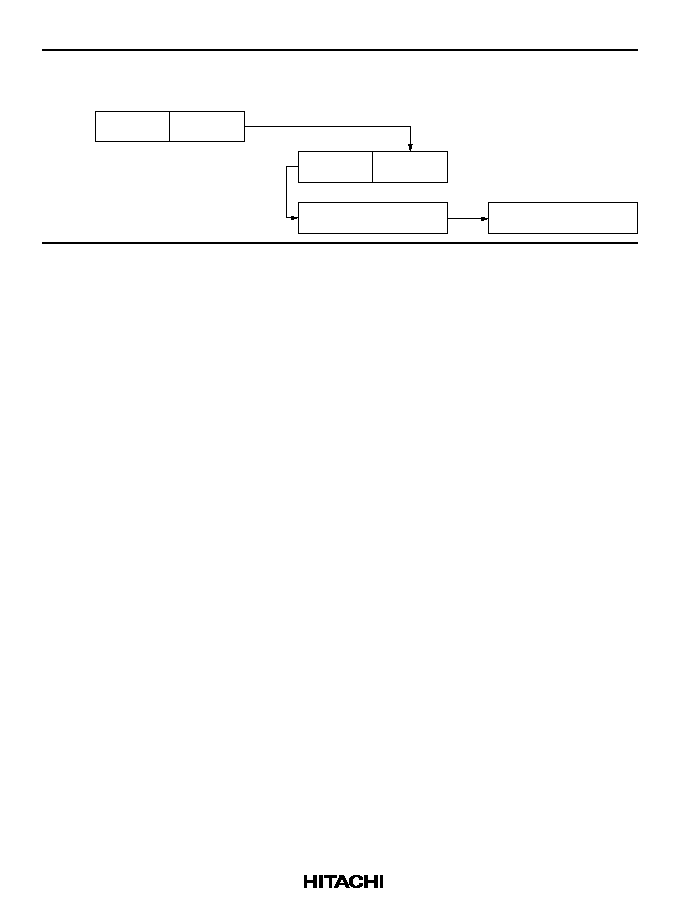
37
No.
Addressing Mode and
Instruction Format
Effective Address
Calculation
Effective Address
8
Memory indirect, @@aa:8
op
8 7
0
15
Memory contents
(16 bits)
0
15
abs
H'00
8 7
0
15
Legend:
reg, regm, regn: Register field
op:
Operation field
disp:
Displacement
IMM:
Immediate data
abs:
Absolute address

38
2.5
Instruction Set
The H8/300 CPU has 57 types of instructions, which are classified by function in table 2.3.
Table 2.3
Instruction Classification
Function
Instructions
Types
Data transfer
MOV, MOVTPE
*
3
, MOVFPE
*
3
, PUSH
*
1
, POP
*
1
3
Arithmetic operations
ADD, SUB, ADDX, SUBX, INC, DEC, ADDS, SUBS,
DAA, DAS, MULXU, DIVXU, CMP, NEG
14
Logic operations
AND, OR, XOR, NOT
4
Shift
SHAL, SHAR, SHLL, SHLR, ROTL, ROTR, ROTXL,
ROTXR
8
Bit manipulation
BSET, BCLR, BNOT, BTST, BAND, BIAND, BOR,
14
BIOR, BXOR, BIXOR, BLD, BILD, BST, BIST
Branch
Bcc
*
2
, JMP, BSR, JSR, RTS
5
System control
RTE, SLEEP, LDC, STC, ANDC, ORC, XORC, NOP
8
Block data transfer
EEPMOV
1
Total 57
Notes:
*
1 PUSH Rn is equivalent to MOV.W Rn, @≠SP.
POP Rn is equivalent to MOV.W @SP+, Rn.
*
2 Bcc is a conditional branch instruction in which cc represents a condition code.
*
3 Not supported by the H8/3337 Series and H8/3397 Series.

39
The following sections give a concise summary of the instructions in each category, and indicate
the bit patterns of their object code. The notation used is defined next.
Operation Notation
RdGeneral register (d
estination)
Rs
General register (source)
Rn
General register
(EAd)
Destination operand
(EAs)
Source operand
SP
Stack pointer
PC
Program counter
CCR
Condition code register
N
N (negative) flag of CCR
Z
Z (zero) flag of CCR
V
V (overflow) flag of CCR
C
C (carry) flag of CCR
#imm
Immediate data
#xx:3
3-bit immediate data
#xx:8
8-bit immediate data
#xx:16
16-bit immediate data
disp
Displacement
+
Addition
≠
Subtraction
◊
Multiplication
˜
Division
Logical AND
Logical OR
Exclusive Logical OR
Move
¨
NOT (logical complement)

40
2.5.1
Data Transfer Instructions
Table 2.4 describes the data transfer instructions. Figure 2.5 shows their object code formats.
Table 2.4
Data Transfer Instructions
Instruction
Size
*
Function
MOV
B/W
(EAs)
Rd, Rs
(EAd)
Moves data between two general registers or between a general
register and memory, or moves immediate data to a general register.
The Rn, @Rn, @(d:16, Rn), @aa:16, #xx:8 or #xx:16, @≠Rn, and
@Rn+ addressing modes are available for byte or word data. The
@aa:8 addressing mode is available for byte data only.
The @≠R7 and @R7+ modes require word operands. Do not specify
byte size for these two modes.
MOVTPE
B
Not supported by the H8/3337 Series and H8/3397 Series.
MOVFPE
B
Not supported by the H8/3337 Series and H8/3397 Series.
PUSH
W
Rn
@≠SP
Pushes a 16-bit general register onto the stack. Equivalent to
MOV.W Rn, @≠SP.
POP
W
@SP+
Rn
Pops a 16-bit general register from the stack. Equivalent to MOV.W
@SP+, Rn.
Note:
*
Size: Operand size
B: Byte
W: Word
41
15
0
8
7
op
rm
rn
MOV
Rm
Rn
15
0
8
7
op
rm
rn
@Rm
Rn
15
0
8
7
op
rm
rn
@(d:16, Rm)
Rn
disp
15
0
8
7
op
rm
rn
@Rm+
Rn,
Rn
@≠Rm
15
0
8
7
op
rn
abs
@aa:8
Rn
15
0
8
7
op
rn
@aa:16
Rn
abs
15
0
8
7
op
rn
IMM
#xx:8
Rn
15
0
8
7
op
rn
#xx:16
Rn
IMM
15
0
8
7
op
rn
POP, PUSH
Legend:
op:
rm, rn:
disp:
abs:
IMM:
Operation field
Register field
Displacement
Absolute address
Immediate data
15
0
8
7
op
rn
MOVFPE, MOVTPE
abs
Figure 2.5 Data Transfer Instruction Codes

42
2.5.2
Arithmetic Operations
Table 2.5 describes the arithmetic instructions. See figure 2.6 in section 2.5.4, Shift Operations,
for their object codes.
Table 2.5
Arithmetic Instructions
Instruction
Size
*
Function
ADD
SUB
B/W
Rd ± Rs
Rd, Rd + #imm
Rd
Performs addition or subtraction on data in two general registers, or
addition on immediate data and data in a general register.
Immediate data cannot be subtracted from data in a general register.
Word data can be added or subtracted only when both words are in
general registers.
ADDX
SUBX
B
Rd ± Rs ± C
Rd, Rd ± #imm ± C
Rd
Performs addition or subtraction with carry or borrow on byte data in
two general registers, or addition or subtraction on immediate data
and data in a general register.
INC
DEC
B
Rd ± #1
Rd
Increments or decrements a general register.
ADDS
SUBS
W
Rd ± #imm
Rd
Adds or subtracts immediate data to or from data in a general
register. The immediate data must be 1 or 2.
DAA
DAS
B
Rd decimal adjust
Rd
Decimal-adjusts (adjusts to packed BCD) an addition or subtraction
result in a general register by referring to the CCR.
MULXU
B
Rd
◊
Rs
Rd
Performs 8-bit
◊
8-bit unsigned multiplication on data in two general
registers, providing a 16-bit result.
DIVXU
B
Rd ˜ Rs
Rd
Performs 16-bit ˜ 8-bit unsigned division on data in two general
registers, providing an 8-bit quotient and 8-bit remainder.
CMP
B/W
Rd ≠ Rs, Rd ≠ #imm
Compares data in a general register with data in another general
register or with immediate data. Word data can be compared only
between two general registers.
NEG
B
0 ≠ Rd
Rd
Obtains the two's complement (arithmetic complement) of data in a
general register.
Note:
*
Size: Operand size
B: Byte
W: Word

43
2.5.3
Logic Operations
Table 2.6 describes the four instructions that perform logic operations. See figure 2.6 in section
2.5.4, Shift Operations, for their object codes.
Table 2.6
Logic Operation Instructions
Instruction
Size
*
Function
AND
B
Rd
Rs
Rd, Rd
#imm
Rd
Performs a logical AND operation on a general register and another
general register or immediate data.
OR
B
Rd
Rs
Rd, Rd
#imm
Rd
Performs a logical OR operation on a general register and another
general register or immediate data.
XOR
B
Rd
Rs
Rd, Rd
#imm
Rd
Performs a logical exclusive OR operation on a general register and
another general register or immediate data.
NOT
B
¨ (Rd)
(Rd)
Obtains the one's complement (logical complement) of general
register contents.
Note:
*
Size: Operand size
B: Byte
2.5.4
Shift Operations
Table 2.7 describes the eight shift instructions. Figure 2.6 shows the object code formats of the
arithmetic, logic, and shift instructions.
Table 2.7
Shift Instructions
Instruction
Size
*
Function
SHAL
B
Rd shift
Rd
SHAR
Performs an arithmetic shift operation on general register contents.
SHLL
B
Rd shift
Rd
SHLR
Performs a logical shift operation on general register contents.
ROTL
B
Rd rotate
Rd
ROTR
Rotates general register contents.
ROTXL
B
Rd rotate through carry
Rd
ROTXR
Rotates general register contents through the C (carry) bit.
Note:
*
Size: Operand size
B: Byte
44
15
0
8
7
op
rm
rn
ADD, SUB, CMP,
ADDX, SUBX (Rm)
Legend:
op:
rm, rn:
IMM:
Operation field
Register field
Immediate data
15
0
8
7
op
rn
ADDS, SUBS, INC, DEC,
DAA, DAS, NEG, NOT
15
0
8
7
op
rn
MULXU, DIVXU
rm
15
0
8
7
rn
IMM
ADD, ADDX, SUBX,
CMP (#xx:8)
op
15
0
8
7
op
rn
AND, OR, XOR (Rm)
rm
15
0
8
7
rn
IMM
AND, OR, XOR (#xx:8)
op
15
0
8
7
rn
SHAL, SHAR, SHLL, SHLR,
ROTL, ROTR, ROTXL, ROTXR
op
Figure 2.6 Arithmetic, Logic, and Shift Instruction Codes

45
2.5.5
Bit Manipulations
Table 2.8 describes the bit-manipulation instructions. Figure 2.7 shows their object code formats.
Table 2.8
Bit-Manipulation Instructions
Instruction
Size
*
Function
BSET
B
1
(<bit no.> of <EAd>)
Sets a specified bit in a general register or memory to 1. The bit is
specified by a bit number, given in 3-bit immediate data or the lower
three bits of a general register.
BCLR
B
0
(<bit no.> of <EAd>)
Clears a specified bit in a general register or memory to 0. The bit is
specified by a bit number, given in 3-bit immediate data or the lower
three bits of a general register.
BNOT
B
¨ (<bit no.> of <EAd>)
(<bit no.> of <EAd>)
Inverts a specified bit in a general register or memory. The bit is
specified by a bit number, given in 3-bit immediate data or the lower
three bits of a general register.
BTST
B
¨ (<bit no.> of <EAd>)
Z
Tests a specified bit in a general register or memory and sets or
clears the Z flag accordingly. The bit is specified by a bit number,
given in 3-bit immediate data or the lower three bits of a general
register.
BAND
B
C
(<bit no.> of <EAd>)
C
ANDs the C flag with a specified bit in a general register or memory.
BIAND
C
[¨ (<bit no.> of <EAd>)]
C
ANDs the C flag with the inverse of a specified bit in a general
register or memory.
The bit number is specified by 3-bit immediate data.
BOR
B
C
(<bit no.> of <EAd>)
C
ORs the C flag with a specified bit in a general register or memory.
BIOR
C
[¨ (<bit no.> of <EAd>)]
C
ORs the C flag with the inverse of a specified bit in a general register
or memory.
The bit number is specified by 3-bit immediate data.
BXOR
B
C
(<bit no.> of <EAd>)
C
XORs the C flag with a specified bit in a general register or memory.
Note:
*
Size: Operand size
B: Byte

46
Instruction
Size
*
Function
BIXOR
B
C
¨ [(<bit no.> of <EAd>)]
C
XORs the C flag with the inverse of a specified bit in a general
register or memory.
The bit number is specified by 3-bit immediate data.
BLD
B
(<bit no.> of <EAd>)
C
Copies a specified bit in a general register or memory to the C flag.
BILD
¨ (<bit no.> of <EAd>)
C
Copies the inverse of a specified bit in a general register or memory
to the C flag.
The bit number is specified by 3-bit immediate data.
BST
B
C
(<bit no.> of <EAd>)
Copies the C flag to a specified bit in a general register or memory.
BIST
¨ C
(<bit no.> of <EAd>)
Copies the inverse of the C flag to a specified bit in a general
register or memory.
The bit number is specified by 3-bit immediate data.
Note:
*
Size: Operand size
B: Byte
Notes on Bit Manipulation Instructions: BSET, BCLR, BNOT, BST, and BIST are read-
modify-write instructions. They read a byte of data, modify one bit in the byte, then write the byte
back. Care is required when these instructions are applied to registers with write-only bits and to
the I/O port registers.
Step
Description
1
Read
Read one data byte at the specified address
2
Modify
Modify one bit in the data byte
3
Write
Write the modified data byte back to the specified address
Example 1: BCLR is executed to clear bit 0 in the port 4 data direction register (P4DDR) under
the following conditions.
P4
7
:
Input pin, low
P4
6
:
Input pin, high
P4
5
≠ P4
0
: Output pins, low
The intended purpose of this BCLR instruction is to switch P4
0
from output to input.
47
Before Execution of BCLR Instruction
P4
7
P4
6
P4
5
P4
4
P4
3
P4
2
P4
1
P4
0
Input/output
Input
Input
Output
Output
Output
Output
Output
Output
Pin state
Low
High
Low
Low
Low
Low
Low
Low
DDR
0
0
1
1
1
1
1
1
DR
1
0
0
0
0
0
0
0
Execution of BCLR Instruction
BCLR #0, @P4DDR
; Clear bit 0 in data direction register
After Execution of BCLR Instruction
P4
7
P4
6
P4
5
P4
4
P4
3
P4
2
P4
1
P4
0
Input/output
Output
Output
Output
Output
Output
Output
Output
Input
Pin state
Low
High
Low
Low
Low
Low
Low
High
DDR
1
1
1
1
1
1
1
0
DR
1
0
0
0
0
0
0
0
Explanation: To execute the BCLR instruction, the CPU begins by reading P4DDR. Since
P4DDR is a write-only register, it is read as H'FF, even though its true value is H'3F.
Next the CPU clears bit 0 of the read data, changing the value to H'FE.
Finally, the CPU writes this value (H'FE) back to P4DDR to complete the BCLR instruction.
As a result, P4
0
DDR is cleared to 0, making P4
0
an input pin. In addition, P4
7
DDR and P4
6
DDR
are set to 1, making P4
7
and P4
6
output pins.
48
15
0
8
7
op
IMM
rn
Operand:
Bit no.:
Legend:
op:
rm, rn:
abs:
IMM:
Operation field
Register field
Absolute address
Immediate data
15
0
8
7
op
rn
BSET, BCLR, BNOT, BTST
register direct (Rn)
immediate (#xx:3)
Operand:
Bit no.:
register direct (Rn)
register direct (Rm)
rm
15
0
8
7
op
0
Operand:
Bit no.:
register indirect (@Rn)
immediate (#xx:3)
rn
0
0
0
0
0
0
0
IMM
15
0
8
7
op
0
Operand:
Bit no.:
register indirect (@Rn)
register direct (Rm)
rn
0
0
0
0
0
0
0
rm
op
15
0
8
7
op
Operand:
Bit no.:
absolute (@aa:8)
immediate (#xx:3)
abs
0
0
0
0
IMM
op
op
15
0
8
7
op
Operand:
Bit no.:
absolute (@aa:8)
register direct (Rm)
abs
0
0
0
0
rm
op
15
0
8
7
op
IMM
rn
Operand:
Bit no.:
register direct (Rn)
immediate (#xx:3)
BAND, BOR, BXOR, BLD, BST
15
0
8
7
op
0
Operand:
Bit no.:
register indirect (@Rn)
immediate (#xx:3)
rn
0
0
0
0
0
0
0
IMM
op
15
0
8
7
op
Operand:
Bit no.:
absolute (@aa:8)
immediate (#xx:3)
abs
0
0
0
0
IMM
op
Figure 2.7 Bit Manipulation Instruction Codes
49
Legend:
op:
rm, rn:
abs:
IMM:
Operation field
Register field
Absolute address
Immediate data
15
0
8
7
op
IMM
rn
Operand:
Bit no.:
register direct (Rn)
immediate (#xx:3)
BIAND, BIOR, BIXOR, BILD, BIST
15
0
8
7
op
0
Operand:
Bit no.:
register indirect (@Rn)
immediate (#xx:3)
rn
0
0
0
0
0
0
0
IMM
op
15
0
8
7
op
Operand:
Bit no.:
absolute (@aa:8)
immediate (#xx:3)
abs
0
0
0
0
IMM
op
Figure 2.7 Bit Manipulation Instruction Codes (cont)

50
2.5.6
Branching Instructions
Table 2.9 describes the branching instructions. Figure 2.8 shows their object code formats.
Table 2.9
Branching Instructions
Instruction
Size
Function
Bcc
--
Branches if condition cc is true.
Mnemonic
cc field
Description
Condition
BRA (BT)
0 0 0 0
Always (true)
Always
BRN (BF)
0 0 0 1
Never (false)
Never
BHI
0 0 1 0
High
C
Z = 0
BLS
0 0 1 1
Low or same
C
Z = 1
BCC (BHS)
0 1 0 0
Carry clear
(High or same)
C = 0
BCS (BLO)
0 1 0 1
Carry set (low)
C = 1
BNE
0 1 1 0
Not equal
Z = 0
BEQ
0 1 1 1
Equal
Z = 1
BVC
1 0 0 0
Overflow clear
V = 0
BVS
1 0 0 1
Overflow set
V = 1
BPL
1 0 1 0
Plus
N = 0
BMI
1 0 1 1
Minus
N = 1
BGE
1 1 0 0
Greater or equal
N
V = 0
BLT
1 1 0 1
Less than
N
V = 1
BGT
1 1 1 0
Greater than
Z
(N
V) = 0
BLE
1 1 1 1
Less or equal
Z
(N
V) = 1
JMP
--
Branches unconditionally to a specified address.
JSR
--
Branches to a subroutine at a specified address.
BSR
--
Branches to a subroutine at a specified displacement from the
current address.
RTS
--
Returns from a subroutine.
51
Legend:
op:
cc:
rm:
disp:
abs:
Operation field
Condition field
Register field
Displacement
Absolute address
15
0
8
7
op
cc
disp
Bcc
15
0
8
7
op
rm
0
JMP (@Rm)
0
0
0
15
0
8
7
op
JMP (@aa:16)
abs
15
0
8
7
op
abs
JMP (@@aa:8)
15
0
8
7
op
disp
BSR
15
0
8
7
op
rm
0
JSR (@Rm)
0
0
0
15
0
8
7
op
JSR (@aa:16)
abs
15
0
8
7
op
abs
JSR (@@aa:8)
15
0
8
7
op
RTS
Figure 2.8 Branching Instruction Codes

52
2.5.7
System Control Instructions
Table 2.10 describes the system control instructions. Figure 2.9 shows their object code formats.
Table 2.10
System Control Instructions
Instruction
Size
*
Function
RTE
--
Returns from an exception-handling routine.
SLEEP
--
Causes a transition to the power-down state.
LDC
B
Rs
CCR, #imm
CCR
Moves immediate data or general register contents to the condition
code register.
STC
B
CCR
Rd
Copies the condition code register to a specified general register.
ANDC
B
CCR
#imm
CCR
Logically ANDs the condition code register with immediate data.
ORC
B
CCR
#imm
CCR
Logically ORs the condition code register with immediate data.
XORC
B
CCR
#imm
CCR
Logically exclusive-ORs the condition code register with immediate
data.
NOP
--
PC + 2
PC
Only increments the program counter.
Note:
*
Size: Operand size
B: Byte
Legend:
op:
rn:
IMM:
Operation field
Register field
Immediate data
15
0
8
7
op
RTE, SLEEP, NOP
15
0
8
7
op
rn
LDC, STC (Rn)
15
0
8
7
op
IMM
ANDC, ORC,
XORC, LDC (#xx:8)
Figure 2.9 System Control Instruction Codes

53
2.5.8
Block Data Transfer Instruction
Table 2.11 describes the EEPMOV instruction. Figure 2.10 shows its object code format.
Table 2.11
Block Data Transfer Instruction
Instruction
Size
Function
EEPMOV
--
if R4L
0 then
repeat
@R5+
@R6+
R4L ≠ 1
R4L
until
R4L = 0
else next;
Moves a data block according to parameters set in general registers
R4L, R5, and R6.
R4L: size of block (bytes)
R5:
starting source address
R6:
starting destination address
Execution of the next instruction starts as soon as the block transfer
is completed.
Legend:
op:
Operation field
15
0
8
7
op
op
Figure 2.10 Block Data Transfer Instruction
54
Notes on EEPMOV Instruction
1. The EEPMOV instruction is a block data transfer instruction. It moves the number of bytes
specified by R4L from the address specified by R5 to the address specified by R6.
R6
R6 + R4L
R5
R5 + R4L
2. When setting R4L and R6, make sure that the final destination address (R6 + R4L) does not
exceed H'FFFF. The value in R6 must not change from H'FFFF to H'0000 during execution of
the instruction.
H'FFFF
Not allowed
R6
R6 + R4L
R5
R5 + R4L

55
2.6
CPU States
2.6.1
Overview
The CPU has three states: the program execution state, exception-handling state, and power-down
state. The power-down state is further divided into three modes: sleep mode, software standby
mode, and hardware standby mode. Figure 2.11 summarizes these states, and figure 2.12 shows a
map of the state transitions.
State
Program execution state
The CPU executes successive program instructions.
Exception-handling state
A transient state triggered by a reset or interrupt. The CPU executes
a hardware sequence that includes loading the program counter from
the vector table.
Power-down state
A state in which some or
all of the chip functions are
stopped to conserve power.
Sleep mode
Software standby mode
Hardware standby mode
Figure 2.11 Operating States

56
Reset state
Hardware
standby mode
Interrupt request
RES
= 1
Power-down state
Sleep mode
Exception-
handling state
Program
execution state
Exception
handling
request
End of exception
handing
SLEEP instruction
with SSBY bit set
STBY
= 1,
RES
= 0
SLEEP
instruction
Software
standby mode
NMI, IRQ
0
to IRQ
2
or IRQ
6
Notes: 1.
2.
A transition to the reset state occurs when
RES
goes low, except when the chip
is in the hardware standby mode.
A transition from any state to the hardware standby mode occurs when
STBY
goes low.
Figure 2.12 State Transitions
2.6.2
Program Execution State
In this state the CPU executes program instructions.
2.6.3
Exception-Handling State
The exception-handling state is a transient state that occurs when the CPU is reset or interrupted
and changes its normal processing flow. In interrupt exception handling, the CPU references the
stack pointer (R7) and saves the program counter and condition code register on the stack. For
further details see section 4, Exception Handling.

57
2.6.4
Power-Down State
The power-down state includes three modes: sleep mode, software standby mode, and hardware
standby mode.
Sleep Mode: Is entered when a SLEEP instruction is executed. The CPU halts, but CPU register
contents remain unchanged and the on-chip supporting modules continue to function.
Software Standby Mode: Is entered if the SLEEP instruction is executed while the SSBY
(Software Standby) bit in the system control register (SYSCR) is set. The CPU and all on-chip
supporting modules halt. The on-chip supporting modules are initialized, but the contents of the
on-chip RAM and CPU registers remain unchanged as long as a specified voltage is supplied. I/O
port outputs also remain unchanged.
Hardware Standby Mode: Is entered when the input at the
STBY
pin goes low. All chip
functions halt, including I/O port output. The on-chip supporting modules are initialized, but on-
chip RAM contents are held.
See section 22, Power-Down State, for further information.
2.7
Access Timing and Bus Cycle
The CPU is driven by the system clock (¯). The period from one rising edge of the system clock to
the next is referred to as a "state." Memory access is performed in a two- or three-state bus cycle.
On-chip memory, on-chip supporting modules, and external devices are accessed in different bus
cycles as described below.
2.7.1
Access to On-Chip Memory (RAM and ROM)
On-chip ROM and RAM are accessed in a cycle of two states designated T
1
and T
2
. Either byte or
word data can be accessed, via a 16-bit data bus. Figure 2.13 shows the on-chip memory access
cycle. Figure 2.14 shows the associated pin states.

58
Bus cycle
Internal data bus (read)
Internal address bus
Internal read signal
Internal write signal
Internal data bus (write)
Address
T
1
state
T
2
state
¯
Write data
Read data
Figure 2.13 On-Chip Memory Access Cycle
Bus cycle
T
1
state
T
2
state
Address
¯
Address bus
AS
: High
RD
: High
WR
: High
Data bus:
High impedance state
Figure 2.14 Pin States during On-Chip Memory Access Cycle
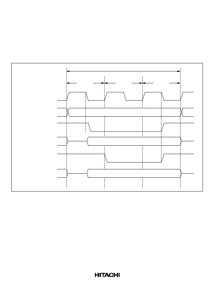
59
2.7.2
Access to On-Chip Supporting Modules and External Devices
The on-chip supporting module registers and external devices are accessed in a cycle consisting of
three states: T
1
, T
2
, and T
3
. Only one byte of data can be accessed per cycle, via an 8-bit data bus.
Access to word data or instruction codes requires two consecutive cycles (six states).
Figure 2.15 shows the access cycle for the on-chip supporting modules. Figure 2.16 shows the
associated pin states. Figures 2.17 (a) and (b) show the read and write access timing for external
devices.
Bus cycle
Internal data bus
(read)
Internal address
bus
Internal read
signal
Internal write
signal
Internal data bus
(write)
¯
Address
Write data
T
1
state
T
2
state
T
3
state
Read data
Figure 2.15 On-Chip Supporting Module Access Cycle
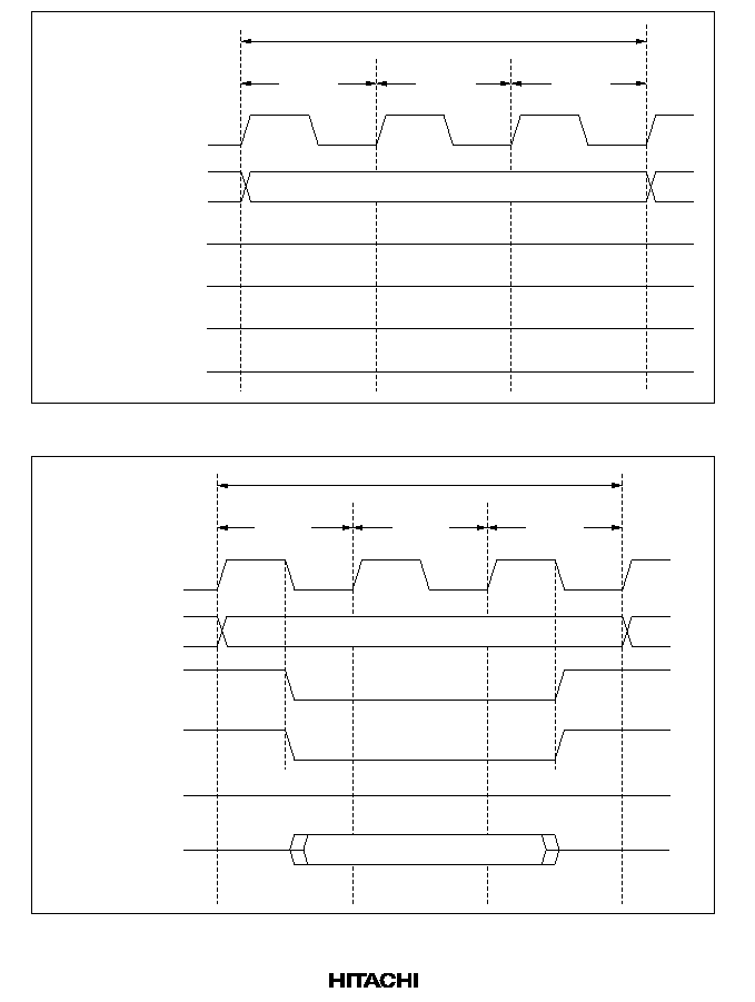
60
Address
Bus cycle
T
3
state
T
2
state
T
1
state
¯
Address bus
AS
: High
RD
: High
WR
: High
Data bus:
High impedance state
Figure 2.16 Pin States during On-Chip Supporting Module Access Cycle
Read cycle
Address
Read data
T
1
state
T
2
state
T
3
state
¯
Address bus
AS
WR
: High
Data bus
RD
Figure 2.17 (a) External Device Access Timing (Read)
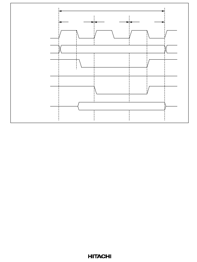
61
Write cycle
Address
Write data
T
1
state
T
2
state
T
3
state
¯
Address bus
AS
WR
Data bus
RD
: High
Figure 2.17 (b) External Device Access Timing (Write)

62

63
Section 3 MCU Operating Modes and Address Space
3.1
Overview
3.1.1
Mode Selection
The H8/3397 and H8/3337 Series operate in three modes numbered 1, 2, and 3. The mode is
selected by the inputs at the mode pins (MD
1
and MD
0
). See table 3.1.
Table 3.1
Operating Modes
Mode
MD
1
MD
0
Address Space
On-Chip ROM
On-chip RAM
Mode 0
Low
Low
--
--
--
Mode 1
Low
High
Expanded
Disabled
Enabled
*
Mode 2
High
Low
Expanded
Enabled
Enabled
*
Mode 3
High
High
Single-chip
Enabled
Enabled
Note:
*
If the RAME bit in the system control register (SYSCR) is cleared to 0, off-chip memory can
be accessed instead.
Modes 1 and 2 are expanded modes that permit access to off-chip memory and peripheral devices.
The maximum address space supported by these externally expanded modes is 64 kbytes.
In mode 3 (single-chip mode), only on-chip ROM and RAM and the on-chip register field are
used. All ports are available for general-purpose input and output.
Mode 0 is inoperative in the H8/3397 and H8/3337 Series. Avoid setting the mode pins to mode 0.
Avoid setting the mode pins to mode 0, and do not change the mode pin settings while the chip is
operating.
3.1.2
Mode and System Control Registers
Table 3.2 lists the registers related to the chip's operating mode: the system control register
(SYSCR) and mode control register (MDCR). The mode control register indicates the inputs to the
mode pins MD
1
and MD
0
.
Table 3.2
Mode and System Control Registers
Name
Abbreviation
Read/Write
Address
System control register
SYSCR
R/W
H'FFC4
Mode control register
MDCR
R
H'FFC5

64
3.2
System Control Register (SYSCR)
Bit
7
6
5
4
3
2
1
0
SSBY
STS2
STS1
STS0
XRST
NMIEG
HIE
RAME
Initial value
0
0
0
0
1
0
0
1
Read/Write
R/W
R/W
R/W
R/W
R
R/W
R/W
R/W
The system control register (SYSCR) is an 8-bit register that controls the operation of the chip.
Bit 7--Software Standby (SSBY): Enables transition to the software standby mode. For details,
see section 22, Power-Down State.
On recovery from software standby mode by an external interrupt, the SSBY bit remains set to 1.
It can be cleared by writing 0.
Bit 7: SSBY
Description
0
The SLEEP instruction causes a transition to sleep mode.
(Initial value)
1
The SLEEP instruction causes a transition to software standby mode.
Bits 6 to 4--Standby Timer Select 2 to 0 (STS2 to STS0): These bits select the clock settling
time when the chip recovers from the software standby mode by an external interrupt. During the
selected time the CPU and on-chip supporting modules continue to stand by. These bits should be
set according to the clock frequency so that the settling time is at least 8 ms. For specific settings,
see section 22.3.3, Clock Settling Time for Exit from Software Standby Mode.
ZTAT and Mask ROM Versions
Bit 6: STS2
Bit 5: STS1
Bit 4: STS0
Description
0
0
0
Settling time = 8,192 states
(Initial value)
1
Settling time = 16,384 states
1
0
Settling time = 32,768 states
1
Settling time = 65,536 states
1
0
--
Settling time = 131,072 states
1
--
Unused

65
F-ZTAT Version
Bit 6: STS2
Bit 5: STS1
Bit 4: STS0
Description
0
0
0
Settling time = 8,192 states
(Initial value)
1
Settling time = 16,384 states
1
0
Settling time = 32,768 states
1
Settling time = 65,536 states
1
0
0
Settling time = 131,072 states
1
Settling time = 1,024 states
1
--
Unused
Note:When 1,024 states (STS2 to STS0 = 101) is selected, the following points should be noted.
If a period exceeding ¯p/1,024 (e.g. ¯p/2,048) is specified when selecting the 8-bit timer,
PWM timer, or watchdog timer clock, the counter in the timer will not count up normally
when 1,024 states is specified for the settling time. To avoid this problem, set the STS value
just before the transition to software standby mode (before executing the SLEEP
instruction), and re-set the value of STS2 to STS0 to a value from 000 to 100 directly after
software standby mode is cleared by an interrupt.
Bit 3--External Reset (XRST): Indicates the source of a reset. A reset can be generated by input
of an external reset signal, or by a watchdog timer overflow when the watchdog timer is used.
XRST is a read-only bit. It is set to 1 by an external reset, and cleared to 0 by watchdog timer
overflow.
Bit 3: NMIEG
Description
0
Reset was caused by watchdog timer overflow.
1
Reset was caused by external input.
(Initial value)
Bit 2--NMI Edge (NMIEG): Selects the valid edge of the
NMI
input.
Bit 2: NMIEG
Description
0
An interrupt is requested on the falling edge of the
NMI
input.
(Initial value)
1
An interrupt is requested on the rising edge of the
NMI
input.
Bit 1--Host Interface Enable (HIE): Enables or disables the host interface function. When
enabled, the host interface processes host-slave data transfers, operating in slave mode.
Bit 1: HIE
Description
0
The host interface is disabled.
(Initial value)
1
The host interface is enabled (slave mode).

66
Bit 0--RAM Enable (RAME): Enables or disables the on-chip RAM. The RAME bit is
initialized by a reset, but is not initialized in the software standby mode.
Bit 0: RAME
Description
0
The on-chip RAM is disabled.
1
The on-chip RAM is enabled.
(Initial value)
3.3
Mode Control Register (MDCR)
Bit
7
6
5
4
3
2
1
0
EXPE
*
1
--
--
--
--
--
MDS1
MDS0
Initial value
--
*
2
1
1
0
0
1
--
*
2
--
*
2
Read/Write
R/W
*
2
--
--
--
--
--
R
R
Notes:
*
1 H8/3337SF (S-mask model, single-power-supply on-chip flash memory version) only.
Otherwise, this is a reserved bit that is always read as 1.
*
2 Determined by the mode pins (MD
1
and MD
0
).
The mode control register (MDCR) is an 8-bit register that indicates the operating mode of the
chip.
Bit 7--Expanded Mode Enable (EXPE): Functions only in the H8/3337SF (S-mask model,
single-power-supply on-chip flash memory version). For details, see section 21.1.6, Mode Control
Register (MDCR).
In models other than the H8/3337SF, this is a reserved bit that cannot be modified and is always
read as 1.
Bits 6 and 5--Reserved: These bits cannot be modified and are always read as 1.
Bits 4 and 3--Reserved: These bits cannot be modified and are always read as 0.
Bit 2--Reserved: This bit cannot be modified and is always read as 1.
Bits 1 and 0--Mode Select 1 and 0 (MDS1 and MDS0): These bits indicate the values of the
mode pins (MD
1
and MD
0
), thereby indicating the current operating mode of the chip. MDS1
corresponds to MD
1
and MDS0 to MD
0
. These bits can be read but not written. When the mode
control register is read, the levels at the mode pins (MD
1
and MD
0
) are latched in these bits.
3.4
Address Space Map in Each Operating Mode
Figures 3.1 to 3.3 show memory maps of the H8/3337Y, H8/3336Y, H8/3334Y, H8/3397,
H8/3396, and H8/3394 in modes 1, 2, and 3.
67
H'FFFF
H'FF88
H'FF87
H'FF80
H'FF7F
H'F780
H'F77F
H'004C
H'004B
H'0000
H'FFFF
H'FF88
H'FF87
H'FF80
H'FF7F
H'F780
H'F77F
H'FFFF
H'FF88
H'FF7F
H'F780
H'EF80
H'EF7F
H'004C
H'004B
H'0000
H'004C
H'004B
H'0000
Mode 1
Expanded Mode without
On-Chip ROM
Mode 2
Expanded Mode with
On-Chip ROM
Mode 3
Single-Chip Mode
Vector table
On-chip ROM,
61,312 bytes
Vector table
Vector table
External address space
On-chip RAM
*
,
2,048 bytes
On-chip RAM,
2,048 bytes
External address space
External address space
External address space
On-chip RAM
*
,
2,048 bytes
On-chip register field
On-chip register field
On-chip register field
External memory can be accessed at these addresses when the RAME bit in
the system control register (SYSCR) is cleared to 0.
Note:
*
On-chip ROM,
63,360 bytes
H'F77F
Figure 3.1 H8/3337Y and H8/3397 Address Space Map
68
H'FFFF
H'FF88
H'FF87
H'FF80
H'FF7F
H'F780
H'F77F
H'004C
H'004B
H'0000
H'FFFF
H'FF88
H'FF87
H'FF80
H'FF7F
H'F780
H'F77F
H'FFFF
H'FF88
H'FF7F
H'F780
H'EF80
H'EF7F
H'004C
H'004B
H'0000
H'004C
H'004B
H'0000
Mode 1
Expanded Mode without
On-Chip ROM
Mode 2
Expanded Mode with
On-Chip ROM
Mode 3
Single-Chip Mode
Vector table
On-chip ROM,
49,152 bytes
Vector table
Vector table
External address space
On-chip RAM
*
,
2,048 bytes
On-chip RAM,
2,048 bytes
External address space
External address space
External address space
On-chip RAM
*
,
2,048 bytes
On-chip register field
On-chip register field
On-chip register field
*
1 Do not access reserved areas.
*
2 External memory can be accessed at these addresses when the RAME bit in
the system control register (SYSCR) is cleared to 0.
Notes:
On-chip ROM,
49,152 bytes
H'F77F
Reserved
*
1
2
Reserved
*
1
2
H'C000
H'C000
H'BFFF
H'BFFF
Figure 3.2 H8/3336Y, H8/3396 Address Space Map
69
H'FFFF
H'FF88
H'FF87
H'FF80
H'FF7F
H'FB80
H'FB7F
H'F780
H'F77F
H'004C
H'004B
H'0000
H'FFFF
H'FF88
H'FF87
H'FF80
H'FF7F
H'FB80
H'FB7F
H'F780
H'F77F
H'FFFF
H'FF88
H'FF7F
H'EF80
H'EF7F
H'8000
H'7FFF
H'8000
H'7FFF
H'004C
H'004B
H'0000
H'004C
H'004B
H'0000
Mode 1
Expanded Mode without
On-Chip ROM
Mode 2
Expanded Mode with
On-Chip ROM
Mode 3
Single-Chip Mode
Vector table
On-chip ROM,
32,768 bytes
Vector table
Vector table
Reserved
*
1
Reserved
*
1,
*
2
Reserved
*
1,
*
2
External address space
On-chip RAM
*
2
,
1,024 bytes
On-chip RAM,
1,024 bytes
External address space
External address space
External address space
On-chip RAM
*
2
,
1,024 bytes
On-chip register field
On-chip register field
On-chip register field
Do not access reserved areas.
External memory can be accessed at these addresses when the RAME bit in
the system control register (SYSCR) is cleared to 0.
Notes:
*
1
*
2
On-chip ROM,
32,768 bytes
Reserved
*
1
Reserved
*
1
H'F780
H'F77F
H'FB80
H'FB7F
Figure 3.3 H8/3334Y, H8/3394 Address Space Map

70

71
Section 4 Exception Handling
4.1
Overview
The H8/3337 Series and H8/3397 Series recognize two kinds of exceptions: interrupts and the
reset. Table 4.1 indicates their priority and the timing of their hardware exception-handling
sequence.
Table 4.1
Hardware Exception-Handling Sequences and Priority
Priority
Type of
Exception
Detection
Timing
Timing of Exception-Handling Sequence
High
Reset
Synchronized
with clock
The hardware exception-handling sequence begins
as soon as
RES
changes from low to high.
Low
Interrupt
End of instruction
execution
*
When an interrupt is requested, the hardware
exception-handling sequence begins at the end of
the current instruction, or at the end of the current
hardware exception-handling sequence.
Note:
*
Not detected after ANDC, ORC, XORC, and LDC instructions.
4.2Reset
4.2.1
Overview
A reset has the highest exception-handling priority. When the
RES pin goes low or when there is a
watchdog timer reset (when the reset option is selected for watchdog timer overflow), all current
processing stops and the chip enters the reset state. The internal state of the CPU and the registers
of the on-chip supporting modules are initialized. The reset exception-handling sequence starts
when
RES returns from low to high, or at the end of a watchdog reset pulse.
4.2.2
Reset Sequence
The reset state begins when
RES goes low or a watchdog reset is generated. To ensure correct
resetting, at power-on the
RES pin should be held low for at least 20 ms. In a reset during
operation, the
RES pin should be held low for at least 10 system clock cycles. The watchdog reset
pulse width is always 518 system clocks. For the pin states during a reset, see appendix D, Port
States in Each Mode.
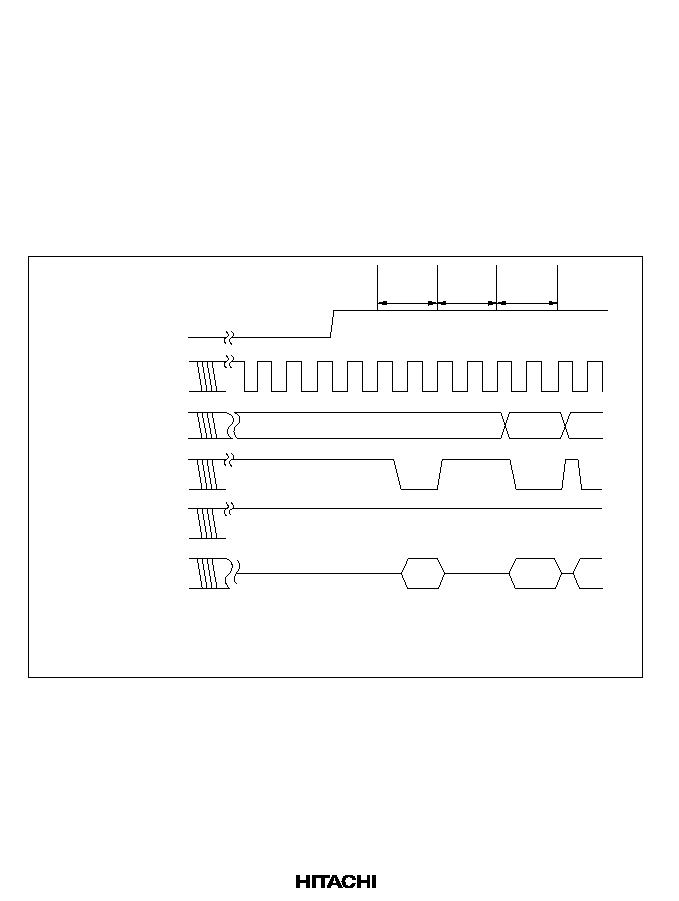
72
The following sequence is carried out when reset exception handling begins.
1. The internal state of the CPU and the registers of the on-chip supporting modules are
initialized, and the I bit in the condition code register (CCR) is set to 1.
2. The CPU loads the program counter with the first word in the vector table (stored at addresses
H'0000 and H'0001) and starts program execution.
The
RES pin should be held low when power is switched off, as well as when power is switched
on.
Figure 4.1 indicates the timing of the reset sequence in modes 2 and 3. Figure 4.2 indicates the
timing in mode 1.
(1)
¯
RES
/watchdog timer
reset (internal)
(2)
Internal address
bus
Internal read
signal
Internal write
signal
Internal data bus
(16 bits)
(1) Reset vector address (H'0000)
(2) Starting address of program
(3) First instruction of program
Vector
fetch
Internal
processing
Instruction
prefetch
(2)
(3)
Figure 4.1 Reset Sequence (Mode 2 or 3, Program Stored in On-Chip ROM)
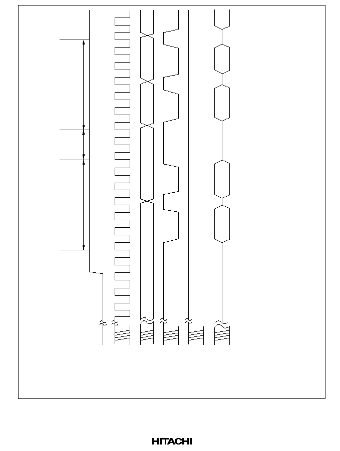
73
(1)
(3)
(5)
(7)
(1), (3) Reset vector address: (1) = H'0000, (3) = H'0001
(2), (4) Starting address of program (contents of reset vector): (2) = upper byte, (4) = lower byte
(5), (7) Starting address of program: (5) = (2) (4), (7) = (2) (4) + 1
(6), (8) First instruction of program: (6) = first byte, (8) = second byte
Vector fetch
Internal
process-
ing
Instruction prefetch
RES
/watchdog timer
reset (internal)
D
7
to D
0
(8 bits)
A
15
to A
0
¯
RD
WR
(2)
(4)
(6)
(8)
Figure 4.2 Reset Sequence (Mode 1)

74
4.2.3
Disabling of Interrupts after Reset
After a reset, if an interrupt were to be accepted before initialization of the stack pointer (SP: R7),
the program counter and condition code register might not be saved correctly, leading to a
program crash. To prevent this, all interrupts, including NMI, are disabled immediately after a
reset. The first program instruction is therefore always executed. This instruction should initialize
the stack pointer (example: MOV.W #xx:16, SP).
After reset exception handling, in order to initialize the contents of CCR, a CCR manipulation
instruction can be executed before an instruction to initialize the stack pointer. Immediately after
execution of a CCR manipulation instruction, all interrupts including NMI are disabled. Use the
next instruction to initialize the stack pointer.
4.3
Interrupts
4.3.1
Overview
The interrupt sources include nine external sources from 23 input pins (NMI, IRQ
0
to IRQ
7
, and
KEYIN
0
to KEYIN
7
), and 26 (H8/3337 Series) or 23 (H8/3397 Series) internal sources in the on-
chip supporting modules. Table 4.2 lists the interrupt sources in priority order and gives their
vector addresses. When two or more interrupts are requested, the interrupt with highest priority is
served first.
The features of these interrupts are:
∑
NMI has the highest priority and is always accepted. All internal and external interrupts except
NMI can be masked by the I bit in the CCR. When the I bit is set to 1, interrupts other than
NMI are not accepted.
∑
IRQ
0
to IRQ
7
can be sensed on the falling edge of the input signal, or level-sensed. The type of
sensing can be selected for each interrupt individually. NMI is edge-sensed, and either the
rising or falling edge can be selected.
∑
All interrupts are individually vectored. The software interrupt-handling routine does not have
to determine what type of interrupt has occurred.
∑
IRQ
6
is multiplexed with 8 external sources (KEYIN
0
to KEYIN
7
). KEYIN
0
to KEYIN
7
can be
masked individually by user software.
∑
The watchdog timer can generate either an NMI or overflow interrupt, depending on the needs
of the application. For details, see section 11, Watchdog Timer.

75
Table 4.2Interrupts
Interrupt source
No.
Vector Table Address
Priority
NMI
IRQ
0
IRQ
1
IRQ
2
IRQ
3
IRQ
4
IRQ
5
IRQ
6
IRQ
7
3
4
5
6
7
8
9
10
11
H'0006 to H'0007
H'0008 to H'0009
H'000A to H'000B
H'000C to H'000D
H'000E to H'000F
H'0010 to H'0011
H'0012 to H'0013
H'0014 to H'0015
H'0016 to H'0017
High
16-bit free-running
timer
ICIA (Input capture A)
ICIB (Input capture B)
ICIC (Input capture C)
ICID (Input capture D)
OCIA (Output compare A)
OCIB (Output compare B)
FOVI (Overflow)
12
13
14
15
16
17
18
H'0018 to H'0019
H'001A to H'001B
H'001C to H'001D
H'001E to H'001F
H'0020 to H'0021
H'0022 to H'0023
H'0024 to H'0025
8-bit timer 0
CMI0A (Compare-match A)
CMI0B (Compare-match B)
OVI0 (Overflow)
19
20
21
H'0026 to H'0027
H'0028 to H'0029
H'002A to H'002B
8-bit timer 1
CMI1A (Compare-match A)
CMI1B (Compare-match B)
OVI1 (Overflow)
22
23
24
H'002C to H'002D
H'002E to H'002F
H'0030 to H'0031
Host interface
*
1
IBF1 (IDR1 receive end)
IBF2 (IDR2 receive end)
25
26
H'0032 to H'0033
H'0034 to H'0035
Serial
communication
interface 0
ERI0 (Receive error)
RXI0 (Receive end)
TXI0 (TDR empty)
TEI0 (TSR empty)
27
28
29
30
H'0036 to H'0037
H'0038 to H'0039
H'003A to H'003B
H'003C to H'003D
Serial
communication
interface 1
ERI1 (Receive error)
RXI1 (Receive end)
TXI1 (TDR empty)
TEI1 (TSR empty)
31
32
33
34
H'003E to H'003F
H'0040 to H'0041
H'0042 to H'0043
H'0044 to H'0045
A/D converter
ADI (Conversion end)
35
H'0046 to H'0047
Watchdog timer
WOVF (WDT overflow)
36
H'0048 to H'0049
I
2
C bus interface
*
2
IICI (Transfer end)
37
H'004A to H'004B
Low
Notes: 1. H'0000 and H'0001 contain the reset vector.
2. H'0002 to H'0005 are reserved in the H8/3337 Series and H8/3397 Series are not
available to the user.
*
1 H8/3337 Series only.
*
2 H8/3337 Series only (option).
76
4.3.2Interrupt-Related Registers
The interrupt-related registers are the system control register (SYSCR), IRQ sense control register
(ISCR), IRQ enable register (IER), and keyboard matrix interrupt mask register (KMIMR).
Table 4.3
Registers Read by Interrupt Controller
Name
Abbreviation
Read/Write
Address
System control register
SYSCR
R/W
H'FFC4
IRQ sense control register
ISCR
R/W
H'FFC6
IRQ enable register
IER
R/W
H'FFC7
Keyboard matrix interrupt mask register
KMIMR
R/W
H'FFF1
System Control Register (SYSCR)
Bit
7
6
5
4
3
2
1
0
SSBY
STS2
STS1
STS0
XRST
NMIEG
HIE
RAME
Initial value
0
0
0
0
1
0
0
1
Read/Write
R/W
R/W
R/W
R/W
R
R/W
R/W
R/W
The valid edge on the
NMI line is controlled by bit 2 (NMIEG) in the system control register.
Bit 2--NMI Edge (NMIEG): Determines whether a nonmaskable interrupt is generated on the
falling or rising edge of the
NMI input signal.
Bit 2: NMIEG
Description
0
An interrupt is generated on the falling edge of
NMI
.
(Initial state)
1
An interrupt is generated on the rising edge of
NMI
.
See section 3.2, System Control Register, for information on the other SYSCR bits.
IRQ Sense Control Register (ISCR)
Bit
7
6
5
4
3
2
1
0
IRQ7SC
IRQ6SC IRQ5SC
IRQ4SC IRQ3SC
IRQ2SC IRQ1SC
IRQ0SC
Initial value
0
0
0
0
0
0
0
0
Read/Write
R/W
R/W
R/W
R/W
R/W
R/W
R/W
R/W

77
Bits 7 to 0--IRQ
7
to IRQ
0
Sense Control (IRQ7SC to IRQ0SC): These bits determine whether
IRQ
7
to
IRQ
0
are level-sensed or sensed on the falling edge.
Bits 7 to 0:
IRQ7SC to IRQ0SC
Description
0
An interrupt is generated when
IRQ
7
to
IRQ
0
inputs are low.
(Initial state)
1
An interrupt is generated by the falling edge of the
IRQ
7
to
IRQ
0
inputs.
IRQ Enable Register (IER)
Bit
7
6
5
4
3
2
1
0
IRQ7E
IRQ6E
IRQ5E
IRQ4E
IRQ3E
IRQ2E
IRQ1E
IRQ0E
Initial value
0
0
0
0
0
0
0
0
R/W
R/W
R/W
R/W
R/W
R/W
R/W
R/W
R/W
Bits 7 to 0--IRQ7 to IRQ0 Enable (IRQ7E to IRQ0E): These bits enable or disable the IRQ
7
to
IRQ
0
interrupts individually.
Bits 7 to 0:
IRQ0E to IRQ7E
Description
0
IRQ
7
to IRQ
0
interrupt requests are disabled.
(Initial state)
1
IRQ
7
to IRQ
0
interrupt requests are enabled.
When edge sensing is selected (by setting bits IRQ7SC to IRQ0SC to 1), it is possible for an
interrupt-handling routine to be executed even though the corresponding enable bit (IRQ7E to
IRQ0E) is cleared to 0 and the interrupt is disabled. If an interrupt is requested while the enable bit
(IRQ7E to IRQ0E) is set to 1, the request will be held pending until served. If the enable bit is
cleared to 0 while the request is still pending, the request will remain pending, although new
requests will not be recognized. If the interrupt mask bit (I) in the CCR is cleared to 0, the
interrupt-handling routine can be executed even though the enable bit is now 0.
If execution of interrupt-handling routines under these conditions is not desired, it can be avoided
by using the following procedure to disable and clear interrupt requests.
1. Set the I bit to 1 in the CCR, masking interrupts. Note that the I bit is set to 1 automatically
when execution jumps to an interrupt vector.
2. Clear the desired bits from IRQ7E to IRQ0E to 0 to disable new interrupt requests.
3. Clear the corresponding IRQ7SC to IRQ0SC bits to 0, then set them to 1 again. Pending IRQn
interrupt requests are cleared when I = 1 in the CCR, IRQnSC = 0, and IRQnE = 0.

78
Keyboard Matrix Interrupt Mask Register (KMIMR)
KMIMR is provided as a register for keyboard matrix interrupt masking. This register controls
interrupts from the
KEYIN
7
to
KEYIN
0
key sense input pins for a 16
◊
8 matrix keyboard.
Bits KMIMR7 to KMIMR0 of KMIMR correspond to key sense inputs
KEYIN
7
to
KEYIN
0
.
In interrupt mask bit initialization, bit KMIMR6 corresponding to the
IRQ
6
/
KEYIN
6
pin is set to
enable interrupt requests, while the other mask bits are set to disable interrupts.
KMIMR is an 8-bit readable/writable register used in keyboard matrix scan/sense. This register
initializes to a state in which only the input at the
IRQ
6
pin is enabled. To enable key sense input
interrupts from two or more pins in keyboard matrix scanning and sensing, clear the corresponding
mask bits to 0.
Figure 4.3 shows the relationship between the IRQ
6
interrupt, KMIMR, and KMIMRA.
Bit
7
6
5
4
3
2
1
0
KMIMR7 KMIMR6 KMIMR5 KMIMR4 KMIMR3 KMIMR2 KMIMR1 KMIMR0
Initial value
1
0
1
1
1
1
1
1
Read/Write
R/W
R/W
R/W
R/W
R/W
R/W
R/W
R/W
Bits 7 to 0--Keyboard Matrix Interrupt Mask (KMIMR7 to KMIMR0): These bits control
key sense input interrupt requests KEYIN
7
to KEYIN
0
.
Bits 7 to 0:
KMIMR7 to KMIMR0
Description
0
Key sense input interrupt request is enabled.
1
Key sense input interrupt request is disabled.
(Initial value)
*
Note:
*
Except KMIMR6, which is initially 0.
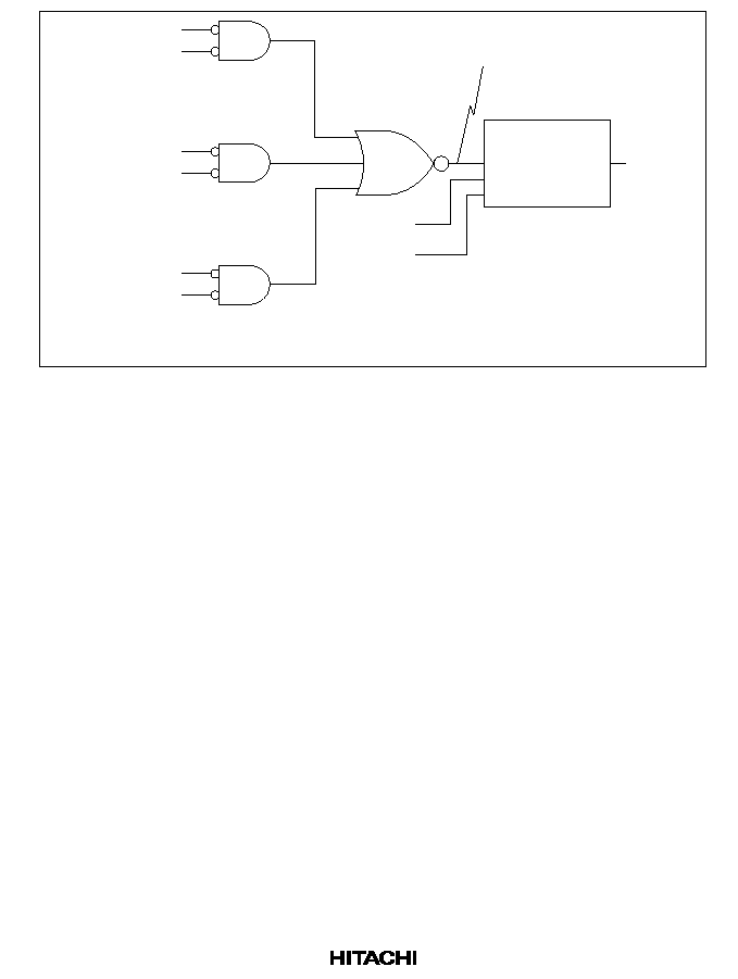
79
IRQ
6
E
IRQ
6
SC
KMIMR0 (1)
P6
0
/
KEYIN
0
KMIMR7 (1)
P6
7
/
KEYIN
7
KMIMR6 (0)
P6
6
/
KEYIN
6
/
IRQ
6
.
.
.
.
.
.
.
.
IRQ
6
internal signal
Edge/level select
and enable/
disable control
IRQ
6
interrupt
Initial values are given in parentheses
Figure 4.3 KMIMR and IRQ
6
Interrupt

80
4.3.3
External Interrupts
The nine external interrupts are NMI and IRQ
0
to IRQ
7
. NMI, IRQ
0
, IRQ
1
, IRQ
2
, and IRQ
6
can be
used to recover from software standby mode.
NMI: A nonmaskable interrupt is generated on the rising or falling edge of the
NMI
input signal
regardless of whether the I (interrupt mask) bit is set in the CCR. The valid edge is selected by the
NMIEG bit in the system control register. The NMI vector number is 3. In the NMI hardware
exception-handling sequence the I bit in the CCR is set to 1.
IRQ
0
to IRQ
7
: These interrupt signals are level-sensed or sensed on the falling edge of the input,
as selected by ISCR bits IRQ0SC to IRQ7SC. These interrupts can be masked collectively by the I
bit in the CCR, and can be enabled and disabled individually by setting and clearing bits IRQ0E to
IRQ7E in the IRQ enable register.
The
IRQ
6
input signal can be logically ORed internally with the key sense input signals. When
KEYIN
0
to
KEYIN
7
pins (P6
0
to P6
7
) are used for key sense input, the corresponding KMIMR bits
should be cleared to 0 to enable the corresponding key sense input interrupts. KMIMR bits
corresponding to unused key sense inputs should be set to 1 to disable the interrupts. All 8 key
sense input interrupts are combined into a single IRQ
6
interrupt.
When one of these interrupts is accepted, the I bit is set to 1. IRQ
0
to IRQ
7
have interrupt vector
numbers 4 to 11. They are prioritized in order from IRQ
7
(low) to IRQ
0
(high). For details, see
table 4.2.
Interrupts IRQ
0
to IRQ
7
do not depend on whether pins
IRQ
0
to
IRQ
7
are input or output pins.
When using external interrupts IRQ
0
to IRQ
7
, clear the corresponding DDR bits to 0 to set these
pins to the input state, and do not use these pins as input or output pins for the timers, serial
communication interface, or A/D converter.
4.3.4
Internal Interrupts
Twenty-six (H8/3337 Series) or twenty-three (H8/3397 Series) internal interrupts can be requested
by the on-chip supporting modules. Each interrupt source has its own vector number, so the
interrupt-handling routine does not have to determine which interrupt has occurred. All internal
interrupts are masked when the I bit in the CCR is set to 1. When one of these interrupts is
accepted, the I bit is set to 1 to mask further interrupts (except
NMI). The vector numbers are 12 to
37. For the priority order, see table 4.2.

81
4.3.5
Interrupt Handling
Interrupts are controlled by an interrupt controller that arbitrates between simultaneous interrupt
requests, commands the CPU to start the hardware interrupt exception-handling sequence, and
furnishes the necessary vector number. Figure 4.4 shows a block diagram of the interrupt
controller.
IRQ0
flag
IRQ0E
IRIC
IEIC
CPU
I (CCR)
NMI interrupt
Interrupt
controller
Priority
decision
IRQ0
interrupt
Interrupt request
Vector number
IICI
interrupt
Note:
*
*
For edge-sensed interrupts, these AND gates change to the circuit shown below.
IRQ0 edge
IRQ0E
S
Q
IRQ0 flag
IRQ0 interrupt
Figure 4.4 Block Diagram of Interrupt Controller
The IRQ interrupts and interrupts from the on-chip supporting modules (except for reset selected
for a watchdog timer overflow) all have corresponding enable bits. When the enable bit is cleared
to 0, the interrupt signal is not sent to the interrupt controller, so the interrupt is ignored. These
interrupts can also all be masked by setting the CPU's interrupt mask bit (I) to 1. Accordingly,
these interrupts are accepted only when their enable bit is set to 1 and the I bit is cleared to 0.
The nonmaskable interrupt (NMI) is always accepted, except in the reset state and hardware
standby mode.

82
When an NMI or another enabled interrupt is requested, the interrupt controller transfers the
interrupt request to the CPU and indicates the corresponding vector number. (When two or more
interrupts are requested, the interrupt controller selects the vector number of the interrupt with the
highest priority.) When notified of an interrupt request, at the end of the current instruction or
current hardware exception-handling sequence, the CPU starts the hardware exception-handling
sequence for the interrupt and latches the vector number.
Figure 4.5 shows the interrupt operation flow.
1. An interrupt request is sent to the interrupt controller when an NMI interrupt occurs, and when
an interrupt occurs on an IRQ input line or in an on-chip supporting module provided the
enable bit of that interrupt is set to 1.
2. The interrupt controller checks the I bit in CCR and accepts the interrupt request if the I bit is
cleared to 0. If the I bit is set to 1 only NMI requests are accepted; other interrupt requests
remain pending.
3. Among all accepted interrupt requests, the interrupt controller selects the request with the
highest priority and passes it to the CPU. Other interrupt requests remain pending.
4. When it receives the interrupt request, the CPU waits until completion of the current
instruction or hardware exception-handling sequence, then starts the hardware exception-
handling sequence for the interrupt and latches the interrupt vector number.
5. In the hardware exception-handling sequence, the CPU first pushes the PC and CCR onto the
stack. See figure 4.6. The stacked PC indicates the address of the first instruction that will be
executed on return from the software interrupt-handling routine.
6. Next the I bit in CCR is set to 1, masking all further interrupts except NMI.
7. The vector address corresponding to the vector number is generated, the vector table entry at
this vector address is loaded into the program counter, and execution branches to the software
interrupt-handling routine at the address indicated by that entry.
Figure 4.7 shows the interrupt timing sequence for the case in which the software interrupt-
handling routine is in on-chip ROM and the stack is in on-chip RAM.
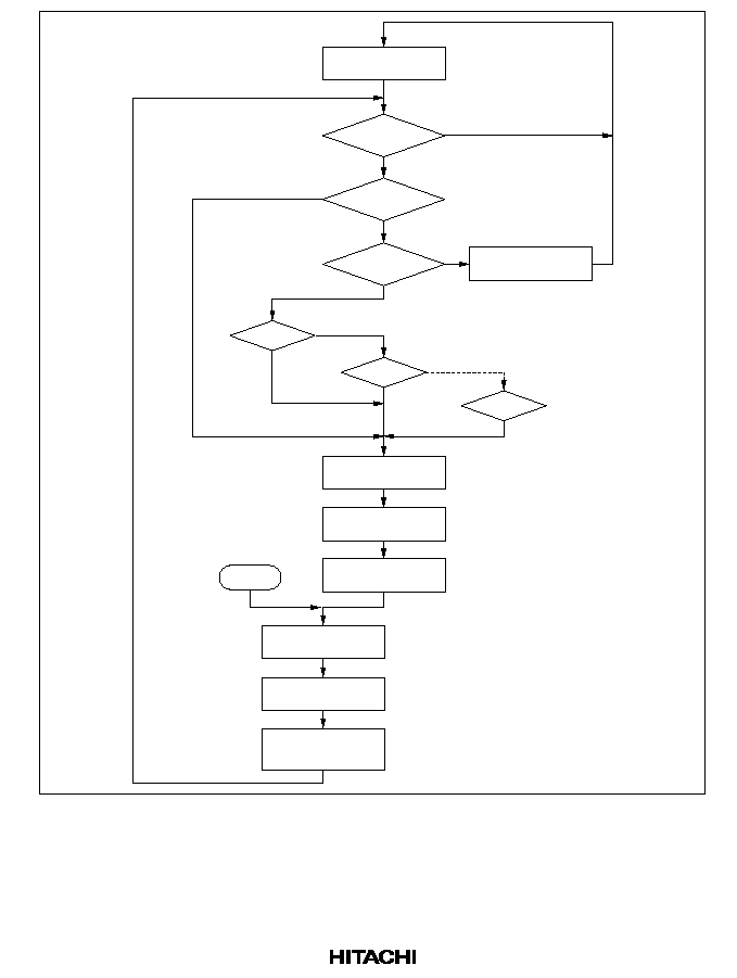
83
Program execution
No
No
No
Yes
No
Yes
Yes
Yes
No
Yes
NMI?
I = 0?
IRQ
0
?
IRQ
1
?
IICI?
Reset
I
1
Interrupt
requested?
Pending
Latch vector no.
Save PC
Save CCR
Read vector address
Branch to software
interrupt-handling
routine
Yes
Figure 4.5 Hardware Interrupt-Handling Sequence

84
SP(R7)
SP ≠ 4
SP ≠ 3
SP ≠ 2
SP ≠ 1
SP (R7)
SP + 1
SP + 2
SP + 3
SP + 4
Even address
CCR
CCR
*
PC
H
Before interrupt
is accepted
After interrupt
is accepted
Pushed onto stack
Upper byte of progam counter
Lower byte of progam counter
Condition code register
Stack pointer
PC
H
:
PC
L
:
CCR:
SP:
The PC contains the address of the first instruction executed after return.
Registers must be saved and restored by word access at an even address.
Notes: 1.
2.
*
Ignored on return.
Stack area
PC
L
Figure 4.6 Usage of Stack in Interrupt Handling
The CCR is comprised of one byte, but when it is saved to the stack, it is treated as one word of
data. During interrupt processing, two identical bytes of CCR data are saved to the stack to create
one word of data. When the RTE instruction is executed to restore the value from the stack, the
byte located at the even address is loaded into CCR, and the byte located at the odd address is
ignored.
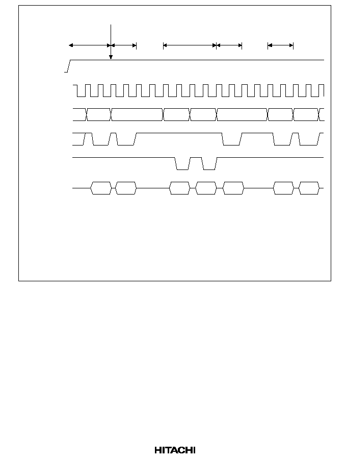
85
(3)
(5)
(6)
(8)
(9)
(1)
Interrupt priority
decision. Wait for
end of instruction.
Interrupt
accepted
Internal
process-
ing
Stack
Vector
fetch
Internal
process-
ing
Instruction prefetch
(first instruction of
interrupt-handling
routine)
Interrupt request
signal
Internal address
bus
Internal write
signal
Internal read
signal
Internal 16-bit
data bus
¯
(1)
(2)
(4)
(7)
(9)
(10)
Instruction
prefetch
(1)
(2) (4)
(3)
(5)
(6)
(7)
(8)
(9)
(10)
Instruction prefetch address (Pushed on stack. Instruction is executed on return from interrupt-handling
routine.)
Instruction code (Not executed)
Instruction prefetch address (Not executed)
SP≠2
SP≠4
CCR
Address of vector table entry
Vector table entry (address of first instruction of interrupt-handling routine)
First instruction of interrupt-handling routine
Figure 4.7 Timing of Interrupt Sequence

86
4.3.6
Interrupt Response Time
Table 4.4 indicates the number of states that elapse from an interrupt request signal until the first
instruction of the software interrupt-handling routine is executed. Since on-chip memory is
accessed 16 bits at a time, very fast interrupt service can be obtained by placing interrupt-handling
routines in on-chip ROM and the stack in on-chip RAM.
Table 4.4
Number of States before Interrupt Service
Number of States
No.
Reason for Wait
On-Chip Memory
External Memory
1
Interrupt priority decision
2
*
3
2
*
3
2
Wait for completion of current
instruction
*
1
1 to 13
5 to 17
*
2
3
Save PC and CCR
4
12
*
2
4
Fetch vector
2
6
*
2
5
Fetch instruction
4
12
*
2
6
Internal processing
4
4
Total
17 to 29
41 to 53
*
2
Notes:
*
1 These values do not apply if the current instruction is EEPMOV.
*
2 If wait states are inserted in external memory access, add the number of wait states.
*
3 1 for internal interrupts.
4.3.7
Precaution
Note that the following type of contention can occur in interrupt handling.
When software clears the enable bit of an interrupt to 0 to disable the interrupt, the interrupt
becomes disabled after execution of the clearing instruction. If an enable bit is cleared by a BCLR
or MOV instruction, for example, and the interrupt is requested during execution of that
instruction, at the instant when the instruction ends the interrupt is still enabled, so after execution
of the instruction, the hardware exception-handling sequence is executed for the interrupt. If a
higher-priority interrupt is requested at the same time, however, the hardware exception-handling
sequence is executed for the higher-priority interrupt and the interrupt that was disabled is ignored.
Similar considerations apply when an interrupt request flag is cleared to 0.

87
Figure 4.8 shows an example in which the OCIAE bit is cleared to 0.
¯
Internal address bus
OCIAE
OCIA exception handling
OCIA interrupt signal
OCFA
CPU write
cycle to TIER
Internal write signal
TIER address
Figure 4.8 Contention between Interrupt and Disabling Instruction
The above contention does not occur if the enable bit or flag is cleared to 0 while the interrupt
mask bit (I) is set to 1.
4.4
Note on Stack Handling
In word access, the least significant bit of the address is always assumed to be 0. The stack is
always accessed by word access. Care should be taken to keep an even value in the stack pointer
(general register R7). Use the PUSH Rn and POP Rn (or MOV.W Rn, @≠SP and MOV.W @SP+,
Rn) instructions to push and pop registers on the stack.
Setting the stack pointer to an odd value can cause programs to crash. Figure 4.9 shows an
example of damage caused when the stack pointer contains an odd address.

88
PC
H
SP
PC
L
H'FECD
H'FECF
H'FECC
BSR instruction
MOV.B R1L, @≠R7
PC is improperly stored
beyond top of stack
H'FECF set in SP
PC
H
is lost
PC
H
:
PC
L
:
R1L:
SP:
Upper byte of program counter
Lower byte of program counter
General register
Stack pointer
SP
R1L
SP
PC
L
Figure 4.9 Example of Damage Caused by Setting an Odd Address in SP

89
Section 5 Wait-State Controller
5.1
Overview
The H8/3337 Series and H8/3397 Series have an on-chip wait-state controller that enables
insertion of wait states into bus cycles for interfacing to low-speed external devices.
5.1.1
Features
Features of the wait-state controller are listed below.
∑
Three selectable wait modes: programmable wait mode, pin auto-wait mode, and pin wait
mode
∑
Automatic insertion of zero to three wait states
5.1.2
Block Diagram
Figure 5.1 shows a block diagram of the wait-state controller.
WAIT
Wait-state controller
(WSC)
WSCR
Internal data bus
Wait request
signal
Legend:
WSCR: Wait-state control register
Figure 5.1 Block Diagram of Wait-State Controller

90
5.1.3
Input/Output Pins
Table 5.1 summarizes the wait-state controller's input pin.
Table 5.1
Wait-State Controller Pins
Name
Abbreviation
I/O
Function
Wait
WAIT
Input
Wait request signal for access to external addresses
5.1.4
Register Configuration
Table 5.2 summarizes the wait-state controller's register.
Table 5.2
Register Configuration
Address
Name
Abbreviation
R/W
Initial Value
H'FFC2
Wait-state control register
WSCR
R/W
H'08
5.2
Register Description
5.2.1
Wait-State Control Register (WSCR)
WSCR is an 8-bit readable/writable register that selects the wait mode for the wait-state controller
(WSC) and specifies the number of wait states. It also controls RAM area setting for dual-power-
supply flash memory, selection/non-selection of single-power-supply flash memory control
registers, and frequency division of the clock signals supplied to the supporting modules.
Bit
7
6
5
4
3
2
1
0
RAMS
*
1
RAM0
*
1
CKDBL
FLSHE
*
2
WMS1
WMS0
WC1
WC0
Initial value
0
0
0
0
1
0
0
0
Read/Write
R/W
R/W
R/W
R/W
R/W
R/W
R/W
R/W
Notes:
*
1 These bits are valid only in the H8/3337YF (dual-power-supply on-chip flash memory
versions).
*
2 This bit is valid only in the H8/3337SF (S-mask model, single-power-supply on-chip
flash memory version).
WSCR is initialized to H'08 by a reset and in hardware standby mode. It is not initialized in
software standby mode.

91
Bit 7--RAM Select (RAMS)
Bit 6--RAM Area Select (RAM0)
Bits 7 and 6 select a RAM area for emulation of dual-power-supply flash memory updates. For
details, see the flash memory description in section 19 and 20, ROM.
Bit 5--Clock Double (CKDBL): Controls frequency division of clock signals supplied to
supporting modules. For details, see section 6, Clock Pulse Generator.
Bit 4--Flash Memory Control Register Enable (FLSHE): Controls selection/non-selection of
single-power-supply flash memory control registers. For details, see the description of flash
memory in section 21, ROM. In models other than the H8/3337SF, this bit is reserved, but it can
be written and read; its initial value is 0.
Bits 3 and 2--Wait Mode Select 1 and 0 (WMS1/0): These bits select the wait mode.
Bit 3: WMS1
Bit 2: WMS0
Description
0
0
Programmable wait mode
1
No wait states inserted by wait-state controller
1
0
Pin wait mode
(Initial value)
1
Pin auto-wait mode
Bits 1 and 0--Wait Count 1 and 0 (WC1/0): These bits select the number of wait states inserted
in access to external address areas.
Bit 1: WC1
Bit 0: WC0
Description
0
0
No wait states inserted by wait-state controller
(Initial value)
1
1 state inserted
1
0
2 states inserted
1
3 states inserted
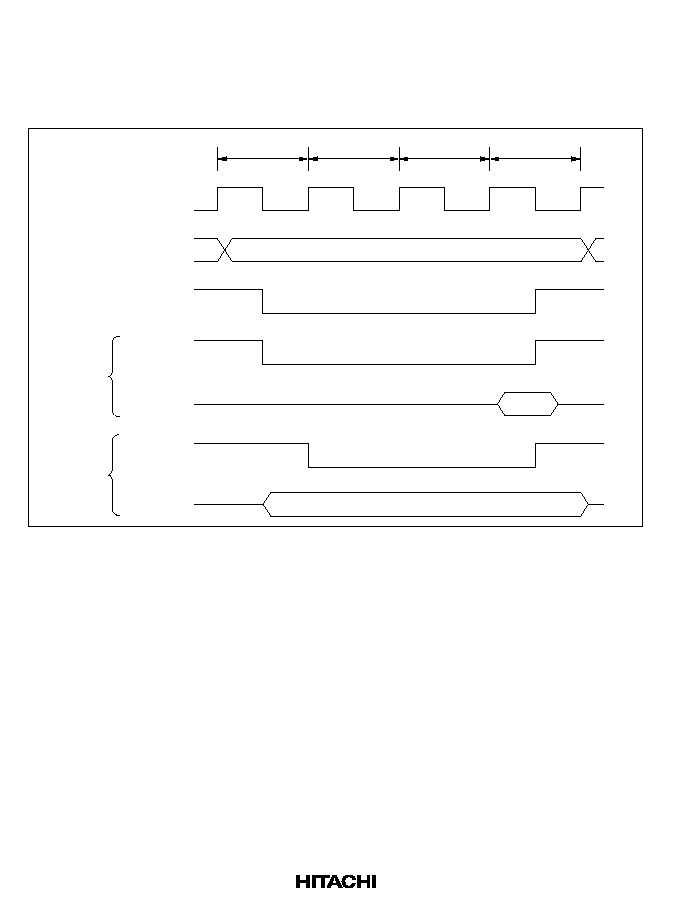
92
5.3
Wait Modes
Programmable Wait Mode: The number of wait states (T
W
) selected by bits WC1 and WC0 are
inserted in all accesses to external addresses. Figure 5.2 shows the timing when the wait count is 1
(WC1 = 0, WC0 = 1).
T
1
T
2
T
W
T
3
¯
Address bus
AS
RD
WR
Data bus
Data bus
External address
Read data
Write data
Read
access
Write
access
Figure 5.2 Programmable Wait Mode
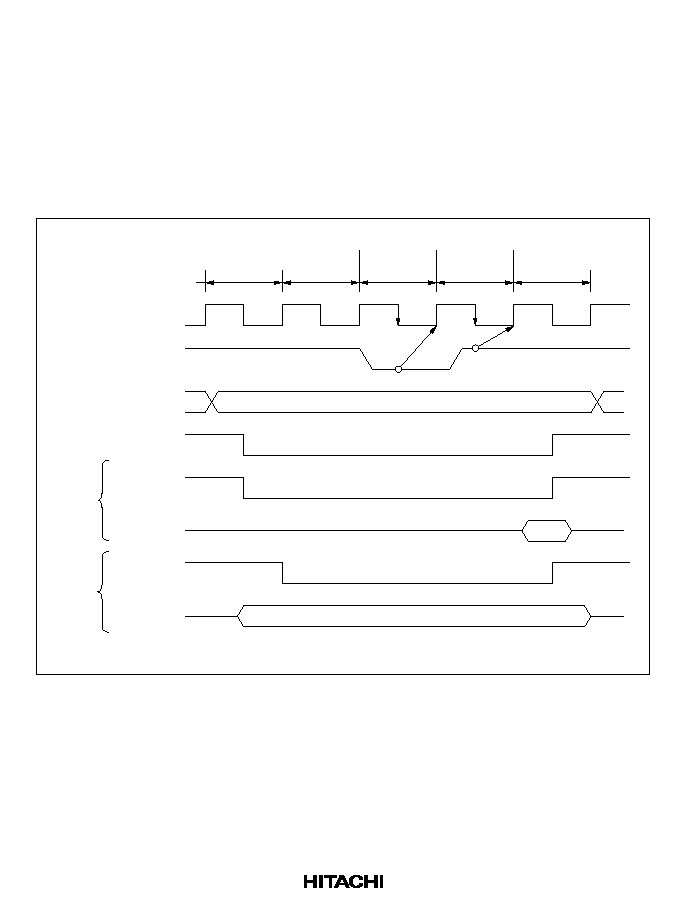
93
Pin Wait Mode: In all accesses to external addresses, the number of wait states (T
W
) selected by
bits WC1 and WC0 are inserted. If the
WAIT pin is low at the fall of the system clock (¯) in the
last of these wait states, an additional wait state is inserted. If the
WAIT pin remains low, wait
states continue to be inserted until the
WAIT signal goes high.
Pin wait mode is useful for inserting four or more wait states, or for inserting different numbers of
wait states for different external devices.
Figure 5.3 shows the timing when the wait count is 1 (WC1 = 0, WC0 = 1) and one additional wait
state is inserted by
WAIT input.
Address bus
Data bus
AS
RD
WR
T
1
T
2
T
W
T
W
T
3
Write data
*
Read data
*
Read
access
Write
access
Note: Arrows indicate time of sampling of the pin.
*
WAIT
¯
pin
WAIT
Data bus
External address
Write data
Inserted by
wait count
Inserted by
signal
WAIT
Figure 5.3 Pin Wait Mode
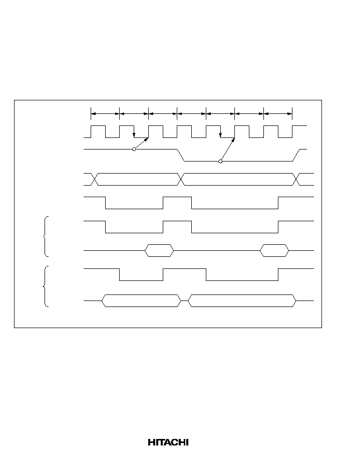
94
Pin Auto-Wait Mode: If the
WAIT pin is low, the number of wait states (T
W
) selected by bits
WC1 and WC0 are inserted.
In pin auto-wait mode, if the
WAIT pin is low at the fall of the system clock (¯) in the T
2
state, the
number of wait states (T
W
) selected by bits WC1 and WC0 are inserted. No additional wait states
are inserted even if the
WAIT pin remains low. Pin auto-wait mode can be used for an easy
interface to low-speed memory, simply by routing the chip select signal to the
WAIT pin.
Figure 5.4 shows the timing when the wait count is 1.
¯
Address bus
Data bus
AS
RD
WR
Data bus
T
1
T
2
T
3
T
1
T
2
T
W
T
3
*
*
Read data
Read data
Write data
Write data
Read
access
Write
access
Note: Arrows indicate time of sampling of the pin.
*
WAIT
External address
External address
WAIT
Figure 5.4 Pin Auto-Wait Mode

95
Section 6 Clock Pulse Generator
6.1
Overview
The H8/3337 Series and H8/3397 Series have a built-in clock pulse generator (CPG) consisting of
an oscillator circuit, a duty adjustment circuit, and a divider and a prescaler that generates clock
signals for the on-chip supporting modules.
6.1.1
Block Diagram
Figure 6.1 shows a block diagram of the clock pulse generator.
XTAL
EXTAL
Oscillator
circuit
Duty
adjustment
circuit
Frequency
divider (1/2)
CKDBL
¯
(system
clock)
¯
P
(for sup-
porting
modules)
Prescaler
¯
P
/2 to ¯
P
/4096
Figure 6.1 Block Diagram of Clock Pulse Generator
Input an external clock signal to the EXTAL pin, or connect a crystal resonator to the XTAL and
EXTAL pins. The system clock frequency (¯) will be the same as the input frequency. This same
system clock frequency (¯
P
) can be supplied to timers and other supporting modules, or it can be
divided by two. The selection is made by software, by controlling the CKDBL bit.

96
6.1.2
Wait-State Control Register (WSCR)
WSCR is an 8-bit readable/writable register that controls frequency division of the clock signals
supplied to the supporting modules. It also controls wait state controller wait settings, RAM area
setting for dual-power-supply flash memory, and selection/non-selection of single-power-supply
flash memory control registers.
WSCR is initialized to H'08 by a reset and in hardware standby mode. It is not initialized in
software standby mode.
Bit
7
6
5
4
3
2
1
0
RAMS
*
1
RAM0
*
1
CKDBL
FLSHE
*
2
WMS1
WMS0
WC1
WC0
Initial value
0
0
0
0
1
0
0
0
Read/Write
R/W
R/W
R/W
R/W
R/W
R/W
R/W
R/W
Notes:
*
1 These bits are valid only in the H8/3337YF (dual-power-supply on-chip flash memory
versions).
*
2This bit is valid only in the H8/3337SF (S-mask model, single-power-supply on-chip
flash memory version).
Bit 7--RAM Select (RAMS)
Bit 6--RAM Area Select (RAM0)
Bits 7 and 6 select a RAM area for emulation of dual-power-supply flash memory updates. For
details, see the flash memory description in section 18, ROM.
Bit 5--Clock Double (CKDBL): Controls the frequency division of clock signals supplied to
supporting modules.
Bit 5: CKDBL
Description
0
The undivided system clock (¯) is supplied as the clock (¯
P
) for supporting
modules.
(Initial value)
1
The system clock (¯) is divided by two and supplied as the clock (¯
P
) for
supporting modules.
Bit 4--Flash Memory Control Register Enable (FLSHE): Controls selection/non-selection of
single-power-supply flash memory control registers. For details, see the description of flash
memory in section 21, ROM. In models other than the H8/3337SF, this bit is reserved, but it can
be written and read; its initial value is 0.
Bits 3 and 2--Wait Mode Select 1 and 0 (WMS1/0)
Bits 1 and 0--Wait Count 1 and 0 (WC1/0)
These bits control wait-state insertion. For details, see section 5, Wait-State Controller.

97
6.2
Oscillator Circuit
6.2.1
Oscillator (Generic Device)
If an external crystal is connected across the EXTAL and XTAL pins, the on-chip oscillator circuit
generates a system clock signal. Alternatively, an external clock signal can be applied to the
EXTAL pin.
Connecting an External Crystal
Circuit Configuration: An external crystal can be connected as in the example in figure 6.2.
Table 6.1 indicates the appropriate damping resistance Rd. An AT-cut parallel resonance crystal
should be used.
EXTAL
XTAL
C
L1
C
L2
C = C = 10 pF to 22 pF
L1 L2
Rd
Figure 6.2 Connection of Crystal Oscillator (Example)
Table 6.1
Damping Resistance
Frequency (MHz)
24
8
10
12
16
Rd max (
)
1 k
500
200
0
0
0
Crystal Oscillator: Figure 6.3 shows an equivalent circuit of the crystal resonator. The crystal
resonator should have the characteristics listed in table 6.2.
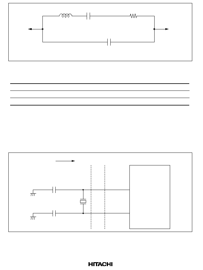
98
XTAL
L
Rs
C
L
C
0
EXTAL
AT-cut parallel resonating crystal
Figure 6.3 Equivalent Circuit of External Crystal
Table 6.2
External Crystal Parameters
Frequency (MHz)
24
8
10
12
16
Rd max (
)
500
12 0
80
70
60
50
C
0
(pF)
7 pF max
7 pF max
7 pF max
7 pF max
7 pF max
7 pF max
Use a crystal with the same frequency as the desired system clock frequency (¯).
Note on Board Design: When an external crystal is connected, other signal lines should be kept
away from the crystal circuit to prevent induction from interfering with correct oscillation. See
figure 6.4. The crystal and its load capacitors should be placed as close as possible to the XTAL
and EXTAL pins.
XTAL
EXTAL
C
L2
C
L1
Not allowed
Signal A
Signal B
Figure 6.4 Board Design around External Crystal
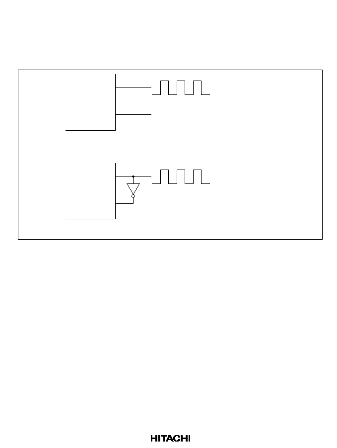
99
Input of External Clock Signal
Circuit Configuration: An external clock signal can be input as shown in the examples in figure
6.5. In example (b) in figure 6.5, the external clock signal should be kept high during standby.
If the XTAL pin is left open, make sure the stray capacitance does not exceed 10 pF.
EXTAL
XTAL
EXTAL
XTAL
74HC04
External clock input
Open
External clock input
(a) Connections with XTAL pin left open
(b) Connections with inverted clock input at XTAL pin
Figure 6.5 External Clock Input (Example)
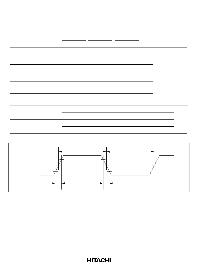
100
External Clock Input: The external clock signal should have the same frequency as the desired
system clock (¯). Clock timing parameters are given in table 6.3 and figure 6.6.
Table 6.3
Clock Timing
V
CC
= 2.7 to
5.5 V
V
CC
= 4.0 to
5.5 V
V
CC
= 5.0 V
±10%
Item
Symbol
Min
Max
Min
Max
Min
Max
Unit
Test Conditions
Low pulse
width of external
clock input
t
EXL
40
--
30
--
20
--
ns
Figure 6.6
High pulse
width of external
clock input
t
EXH
40
--
30
--
20
--
ns
External clock
rise time
t
EXr
--
10
--
10
--
5
ns
External clock
fall time
t
EXf
--
10
--
10
--
5
ns
Clock pulse
t
CL
0.3
0.7
0.3
0.7
0.3
0.7
t
cyc
¯
5 MHz Figure
width low
0.4
0.6
0.4
0.6
0.4
0.6
t
cyc
¯ < 5 MHz 20-4
Clock pulse
t
CH
0.3
0.7
0.3
0.7
0.3
0.7
t
cyc
¯
5 MHz
width high
0.4
0.6
0.4
0.6
0.4
0.6
t
cyc
¯ < 5 MHz
t
EXH
t
EXL
t
EXt
t
EXr
V
CC
◊
0.5
EXTAL
Figure 6.6 External Clock Input Timing
Table 6.4 shows the external clock output settling delay time. Figure 6.7 shows the timing for the
external clock output settling delay time. The oscillator and duty correction circuit have the
function of regulating the waveform of the external clock input to the EXTAL pin. When the
specified clock signal is input to the EXTAL pin, internal clock signal output is confirmed after
the elapse of the external clock output settling delay time (t
DEXT
). As clock signal output is not
confirmed during the t
DEXT
period, the reset signal should be driven low and the reset state
maintained during this time.

101
Table 6.4
External Clock Output Settling Delay Time
Conditions: V
CC
= 2.7 to 5.5 V, AV
CC
= 2.7 to 5.5 V, V
SS
= AV
SS
= 0 V
Item
Symbol
Min
Max
Unit
Notes
External clock output settling
delay time
t
DEXT
*
500
--
µs
Figure 6.7
Note:
*
t
DEXT
includes a 10 t
cyc
RES
pulse width (t
RESW
).
V
CC
STBY
EXTAL
¯ (internal or
external)
RES
t
DEXT
*
Note:
*
t
DEXT
includes a 10 t
cyc
RES
pulse width (t
RESW
).
2.7 V
V
IH
Figure 6.7 External Clock Output Settling Delay Time
6.2.2
Oscillator Circuit (H8/3337SF)
If an external crystal is connected across the EXTAL and XTAL pins, the on-chip oscillator circuit
generates a system clock signal. Alternatively, an external clock signal can be applied to the
EXTAL pin.
Connecting an External Crystal
Circuit Configuration: An external crystal can be connected as in the example in figure 6.8.
Table 6.5 indicates the appropriate damping resistance Rd. An AT-cut parallel resonance crystal
should be used.
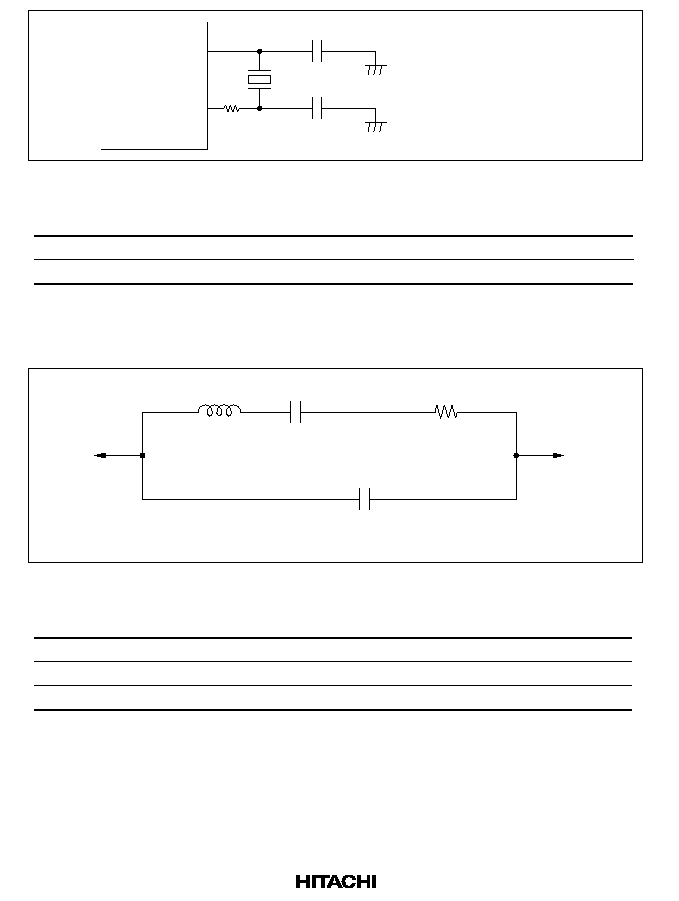
102
EXTAL
XTAL
C
L1
C
L2
C
L1
= C
L2
= 10 pF to 22 pF
Rd
Figure 6.8 Connection of Crystal Oscillator (Example)
Table 6.5
Damping Resistance
Frequency (MHz)
24
8
10
Rd max (
)
1 k
500
200
0
Crystal Oscillator: Figure 6.9 shows an equivalent circuit of the crystal resonator. The crystal
resonator should have the characteristics listed in table 6.6.
XTAL
L
Rs
C
L
C
0
EXTAL
AT-cut parallel resonating crystal
Figure 6.9 Equivalent Circuit of External Crystal
Table 6.6
External Crystal Parameters
Frequency (MHz)
24
8
10
Rs max (
)
500
120
80
70
C
0
(pF)
7 pF max
7 pF max
7 pF max
7 pF max
Use a crystal with the same frequency as the desired system clock frequency (¯).
Note on Board Design: When an external crystal is connected, other signal lines should be kept
away from the crystal circuit to prevent induction from interfering with correct oscillation. See
figure 6.10. The crystal and its load capacitors should be placed as close as possible to the XTAL
and EXTAL pins.
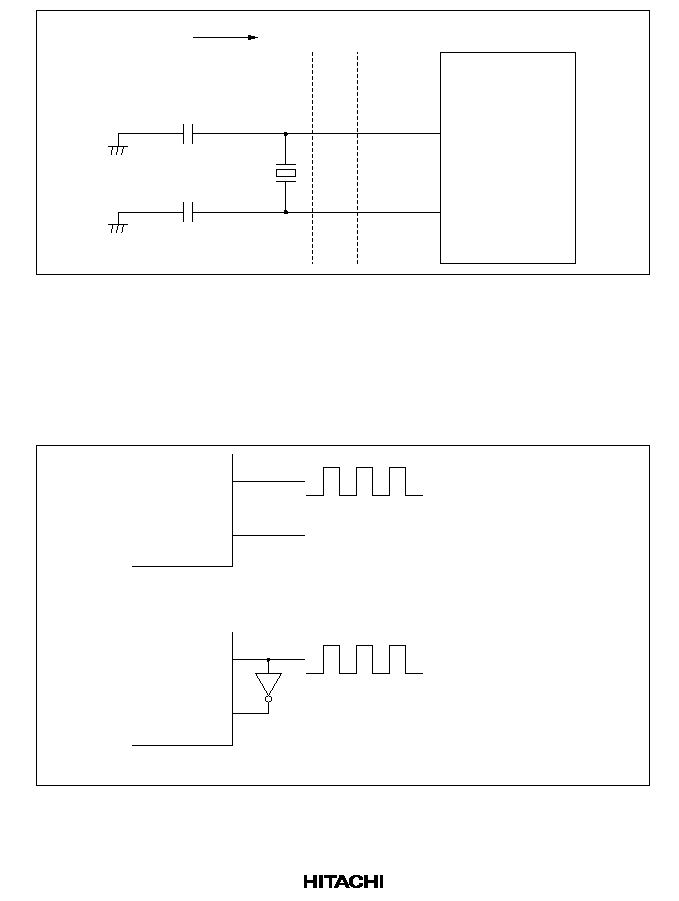
103
XTAL
EXTAL
C
L2
C
L1
Not allowed
Signal A
Signal B
Figure 6.10 Notes on Board Design around External Crystal
Input of External Clock Signal
Circuit Configuration: An external clock signal can be input as shown in the examples in figure
6.11. In example (b) in figure 6.11, the external clock signal should be kept high during standby.
If the XTAL pin is left open, make sure the stray capacitance does not exceed 10 pF.
EXTAL
XTAL
EXTAL
XTAL
74HC04
External clock input
Open
External clock input
(a) Connections with XTAL pin left open
(b) Connections with inverted clock input at XTAL pin
Figure 6.11 External Clock Input (Example)

104
External Clock Input: The external clock signal should have the same frequency as the desired
system clock (¯). Clock timing parameters are given in table 6.7 and figure 6.12.
Table 6.7
Clock Timing
V
CC
= 3.0 to 5.5 V
Item
Symbol
Min
Max
Unit
Test Conditions
Low pulse width of external
clock input
t
EXL
40
--
ns
Figure 6.12
High pulse width of external
clock input
t
EXH
40
--
ns
External clock rise time
t
EXr
--
10
ns
External clock fall time
t
EXf
--
10
ns
Clock pulse
t
CL
0.3
0.7
t
cyc
¯
5 MHz
Figure 23.7
width low
0.4
0.6
t
cyc
¯ < 5 MHz
Clock pulse
t
CH
0.3
0.7
t
c yc
¯
5 MHz
width high
0.4
0.6
t
cyc
¯ < 5 MHz
t
EXH
t
EXL
t
EXt
t
EXr
V
CC
◊
0.5
EXTAL
Figure 6.12 External Clock Input Timing
Table 6.8 lists the external clock output stabilization delay time. Figure 6.13 shows the timing for
the external clock output stabilization delay time. The oscillator and duty correction circuit have
the function of regulating the waveform of the external clock input to the EXTAL pin. When the
specified clock signal is input to the EXTAL pin, internal clock signal output is confirmed after
the elapse of the external clock output stabilization delay time (t
DEXT
). As clock signal output is not
confirmed during the t
DEXT
period, the reset signal should be driven low and the reset state
maintained during this time.
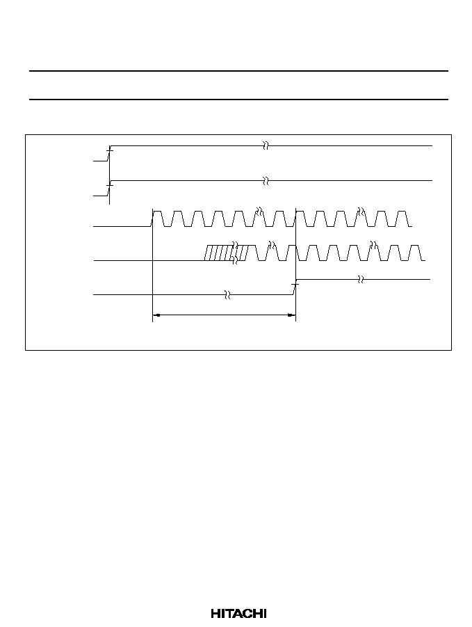
105
Table 6.8
External Clock Output Stabilization Delay Time
Conditions: V
CC
= 3.0 to 5.5 V, AV
CC
= 2.7 to 5.5 V, V
SS
= AV
SS
= 0 V
Item
Symbol
Min
Max
Unit
Notes
External clock output stabilization
delay time
t
DEXT
*
500
--
µs
Figure 6.13
Note:
*
t
DEXT
includes a 10 t
cyc
RES
pulse width (t
RESW
).
V
CC
STBY
EXTAL
¯ (internal and
external)
RES
t
DEXT
*
Note:
*
t
DEXT
includes a 10 t
cyc
RES
pulse width (t
RESW
).
3.0 V
V
IH
Figure 6.13 External Clock Output Stabilization Delay Time
6.3
Duty Adjustment Circuit
When the clock frequency is 5 MHz or above, the duty adjustment circuit adjusts the duty cycle of
the signal from the oscillator circuit to generate the system clock (¯).
6.4
Prescaler
The clock for the on-chip supporting modules (¯
P
) has either the same frequency as the system
clock (¯) or this frequency divided by two, depending on the CKDBL bit. The prescaler divides
the frequency of ¯
P
to generate internal clock signals with frequencies from ¯
P
/2 to ¯
P
/4096.

106

107
Section 7 I/O Ports
7.1
Overview
The H8/3337 Series and H8/3397 Series have six 8-bit input/output ports, one 7-bit input/output
port, and one 3-bit input/output port, and one 8-bit dedicated input port.
Table 7.1 lists the functions of each port in each operating mode. As table 7.1 indicates, the port
pins are multiplexed, and the pin functions differ depending on the operating mode.
Each port has a data direction register (DDR) that selects input or output, and a data register (DR)
that stores output data. If bit manipulation instructions will be executed on the port data direction
registers, see "Notes on Bit Manipulation Instructions" in section 2.5.5, Bit Manipulation
Instructions.
Ports 1, 2, 3, 4, 6, and 9 can drive one TTL load and a 90-pF capacitive load. Ports 5 and 8 can
drive one TTL load and a 30-pF capacitive load. Ports 1 and 2 can drive LEDs (with 10-mA
current sink). Ports 1 to 6, 8, and 9 can drive a darlington pair. Ports 1 to 3, and 6 have built-in
MOS pull-up transistors.
For block diagrams of the ports, see appendix C, I/O Port Block Diagrams.
Pin P8
6
of port 8 and pin P9
7
of port 9 can drive a bus buffer. For details of bus buffer drive, see
section 13, I
2
C Bus Interface.

108
Table 7.1 (a) Port Functions for H8/3337 Series
Expanded
Modes
Single-Chip
Mode
Port
Description
Pins
Mode 1
Mode 2
Mode 3
Port 1
∑
8-bit I/O port
∑
Can drive LEDs
∑
Built-in input
pull-ups
P1
7
to P1
0
/A
7
to A
0
Lower address
output (A
7
to A
0
)
Lower address
output (A
7
to A
0
)
or general input
General
input/output
(Can also be
used as Key-
scan output
port)
Port 2
∑
8-bit I/O port
∑
Can drive LEDs
∑
Built-in input
pull-ups
P2
7
to P2
0
/A
15
to A
8
Upper address
output (A
15
to A
8
)
Upper address
output (A
15
to A
8
)
or general input
General
input/output
(Can also be
used as Key-
scan output
port)
Port 3
∑
8-bit I/O port
∑
Built-in input
pull-ups
∑
HIF data bus
P3
7
to P3
0
/
HDB
7
to HDB
0
/
D
7
to D
0
Data bus
(D
7
to D
0
)
Data bus
(D
7
to D
0
)
HIF data bus
(HDB
7
to
HDB
0
) or
general input/
output
Port 4
∑
8-bit I/O port
P4
7
/PW
1
P4
6
/PW
0
PWM timer 0/1 output (PW
0
, PW
1
), or general input/
output
P4
5
/TMRI
1
/HIRQ
12
P4
4
/TMO
1
/HIRQ
1
P4
3
/TMCI
1
/HIRQ
11
8-bit timer 1 input/output (TMCI
1
, TMO
1
, TMRI
1
), host
processor interrupt request output from HIF (HIRQ
11
,
HIRQ
1
, HIRQ
12
), or general input/output
P4
2
/TMRI
0
P4
1
/TMO
0
P4
0
/TMCI
0
8-bit timer 0 input/output (TMCI
0
, TMO
0
, TMRI
0
) or
general input/output
Port 5
∑
3-bit I/O port
P5
2
/SCK
0
P5
1
/RxD
0
P5
0
/TxD
0
Serial communication interface 0 input/output (TxD
0
,
RxD
0
, SCK
0
) or general input/output
Port 6
∑
8-bit I/O port
∑
Built-in input
pull-ups
∑
Key sense
interrupt input
P6
7
/
IRQ
7
/
KEYIN
7
P6
6
/FTOB/
IRQ
6
/
KEYIN
6
P6
5
/FTID/
KEYIN
5
P6
4
/FTIC/
KEYIN
4
P6
3
/FTIB/
KEYIN
3
P6
2
/FTIA/
KEYIN
2
P6
1
/FTOA/
KEYIN
1
P6
0
/FTCI/
KEYIN
0
16-bit free-running timer input/output (FTCI, FTOA,
FTIA, FTIB, FTIC, FTID, FTOB), key sense interrupt
input (
KEYIN
7
to
KEYIN
0
), external interrupt input (
IRQ
7
,
IRQ
6
), or general input/output

109
Expanded
Modes
Single-Chip
Mode
Port
Description
Pins
Mode 1
Mode 2
Mode 3
Port 7
∑
8-bit input port
P7
7
/AN
7
/DA
1
P7
6
/AN
6
/DA
0
A/D converter analog input (AN
7
, AN
6
), D/A converter
analog output (DA
1
, DA
0
), or general input
P7
5
to P7
0
AN
5
to AN
0
A/D converter analog input (AN
5
to AN
0
) or general input
Port 8
∑
7-bit I/O port
∑
Bus buffer drive
capability (P8
6
)
P8
6
/
IRQ
5
/SCK
1
/SCL
P8
5
/
CS
2
/
IRQ
4
/RxD
1
P8
4
/
IOW
/
IRQ
3
/TxD
1
Serial communication interface 1 input/output (TxD
1
,
RxD
1
, SCK
1
), HIF control input/output (
CS
2
/
IOW
), I
2
C
clock input/output (SCL), external interrupt input (
IRQ
5
,
IRQ
4
,
IRQ
3
) or general input/output
P8
3
/
IOR
P8
2
/
CS
1
P8
1
/GA
20
P8
0
/HA
0
HIF control input/output (HA
0
, GA
20
, CS
1
, IOR), or
general input/output
Port 9
∑
8-bit I/O port
∑
Bus buffer drive
capability (P9
7
)
P9
7
/
WAIT
/SDA
Expanded data bus control input
(
WAIT
), I
2
C data input/output (SDA), or
general input/output
I
2
C data
input/output
(SDA) or
general input/
output
P9
6
/¯
System clock (¯)
output
System clock (¯)
output
¯ output or
general input
P9
5
/
AS
P9
4
/
WR
P9
3
/
RD
Expanded
data bus
(
RD
,
WR
,
AS
)
Expanded
data bus
(
RD
,
WR
,
AS
)
General
input/output
P9
2
/
IRQ
0
P9
1
/
IRQ
1
/
EIOW
P9
0
/
ADTRG
/
IRQ
2
/
ECS
2
HIF control input/output (
ECS
2
,
EIOW
), A/D converter
trigger input (
ADTRG
), external interrupt (
IRQ
2
to
IRQ
0
),
or general input/output

110
Table 7.1 (b) Port Functions for H8/3397 Series
Expanded
Modes
Single-Chip
Mode
Mode 3
Port
Description
Pins
Mode 1
Mode 2
Master Mode
Port 1
∑
8-bit I/O port
∑
Can drive LEDs
∑
Built-in input pull-
ups
P1
7
to P1
0
/A
7
to A
0
Lower address
output (A
7
to A
0
)
Lower address
output (A
7
to A
0
)
or general input
General
input/output
(Can also be
used as Key-
scan output
port)
Port 2
∑
8-bit I/O port
∑
Can drive LEDs
∑
Built-in input
pull-ups
P2
7
to P2
0
/A
15
to A
8
Upper address
output (A
15
to A
8
)
Upper address
output (A
15
to A
8
)
or general input
General
input/output
(Can also be
used as Key-
scan output
port)
Port 3
∑
8-bit I/O port
∑
Built-in input
pull-ups
P3
7
to P3
0
/D
7
to D
0
Data bus
(D
7
to D
0
)
Data bus
(D
7
to D
0
)
General
input/output
Port 4
∑
8-bit I/O port
P4
7
/PW
1
P4
6
/PW
0
PWM timer 0/1 output (PW
0
, PW
1
), or general
input/output
P4
5
/TMRI
1
P4
4
/TMO
1
P4
3
/TMCI
1
8-bit timer 1 input/output (TMCI
1
, TMO
1
, TMRI
1
), or
general input/output
P4
2
/TMRI
0
P4
1
/TMO
0
P4
0
/TMCI
0
8-bit timer 0 input/output (TMCI
0
, TMO
0
, TMRI
0
) or
general input/output
Port 5
∑
3-bit I/O port
P5
2
/SCK
0
P5
1
/RxD
0
P5
0
/TxD
0
Serial communication interface 0 input/output (TxD
0
,
RxD
0
, SCK
0
) or general input/output
Port 6
∑
8-bit I/O port
∑
Built-in input
pull-ups
P6
7
/
IRQ
7
/
KEYIN
7
P6
6
/FTOB/
IRQ
6
/
KEYIN
6
P6
5
/FTID/
KEYIN
5
P6
4
/FTIC/
KEYIN
4
P6
3
/FTIB/
KEYIN
3
P6
2
/FTIA/
KEYIN
2
P6
1
/FTOA/
KEYIN
1
P6
0
/FTCI/
KEYIN
0
16-bit free-running timer input/output (FTCI, FTOA,
FTIA, FTIB, FTIC, FTID, FTOB), key sense interrupt
input (
KEYIN
7
to
KEYIN
0
), external interrupt input (
IRQ
7
,
IRQ
6
), or general input/output
Port 7
∑
8-bit input port
P7
7
to P7
0
/AN
7
to AN
0
A/D converter analog input (AN
7
to AN
0
) or general input

111
Expanded
Modes
Single-Chip
Mode
Mode 3
Port
Description
Pins
Mode 1
Mode 2
Master Mode
Port 8
∑
7-bit I/O port
P8
6
/
IRQ
5
/SCK
1
P8
5
/
IRQ
4
/RxD
1
P8
4
/
IRQ
3
/TxD
1
Serial communication interface 1 input/output (TxD
1
,
RxD
1
, SCK
1
), external interrupt input (
IRQ
5
,
IRQ
4
,
IRQ
3
),
or general input/output
P8
3
P8
2
P8
1
P8
0
General
input/output
General
input/output
General
input/output
Port 9
∑
8-bit I/O port
P9
7
/
WAIT
Expanded data bus control input
(
WAIT
), or general input/output
General
input/output
P9
6
/¯
System clock (¯)
output
System clock (¯)
output
¯ output or
general input
P9
5
/
AS
P9
4
/
WR
P9
3
/
RD
Expanded data
bus control output
(
RD
,
WR
,
AS
)
Expanded data
bus control output
(
RD
,
WR
,
AS
)
General
input/output
P9
2
/
IRQ
0
P9
1
/
IRQ
1
External interrupt (
IRQ
0
,
IRQ
1
) or general input/output
P9
0
/
ADTRG
/
IRQ
2
A/D converter external trigger input (
ADTRG
), external
interrupt input (
IRQ
2
), or general input/output
112
7.2Port 1
7.2.1
Overview
Port 1 is an 8-bit input/output port with the pin configuration shown in figure 7.1. The pin
functions differ depending on the operating mode.
Port 1 has built-in, software-controllable MOS input pull-up transistors that can be used in modes
2 and 3.
Pins in port 1 can drive one TTL load and a 90-pF capacitive load. They can also drive LEDs and
darlington transistors.
P1
7
/A
7
P1
6
/A
6
P1
5
/A
5
P1
4
/A
4
P1
3
/A
3
P1
2
/A
2
P1
1
/A
1
P1
0
/A
0
Port 1
Port 1 pins
A
7
(output)
A
6
(output)
A
5
(output)
A
4
(output)
A
3
(output)
A
2
(output)
A
1
(output)
A
0
(output)
Pin configuration
in mode 1
(expanded mode
with on-chip ROM
disabled)
A
7
(output)/P1
7
(input)
A
6
(output)/P1
6
(input)
A
5
(output)/P1
5
(input)
A
4
(output)/P1
4
(input)
A
3
(output)/P1
3
(input)
A
2
(output)/P1
2
(input)
A
1
(output)/P1
1
(input)
A
0
(output)/P1
0
(input)
Pin configuration
in mode 2
(expanded mode
with on-chip ROM
enabled)
P1
7
(input/output)
P1
6
(input/output)
P1
5
(input/output)
P1
4
(input/output)
P1
3
(input/output)
P1
2
(input/output)
P1
1
(input/output)
P1
0
(input/output)
Pin configuration in mode 3
(single-chip mode)
Figure 7.1 Port 1 Pin Configuration

113
7.2.2
Register Configuration and Descriptions
Table 7.2 summarizes the port 1 registers.
Table 7.2Port 1 Registers
Name
Abbreviation
Read/Write
Initial Value
Address
Port 1 data direction register
P1DDR
W
H'FF (mode 1)
H'00 (modes 2 and 3)
H'FFB0
Port 1 data register
P1DR
R/W
H'00
H'FFB2
Port 1 input pull-up control
register
P1PCR
R/W
H'00
H'FFAC
Port 1 Data Direction Register (P1DDR)
Bit
7
6
5
4
3
2
1
0
P1
7
DDR
P1
6
DDR P1
5
DDR
P1
4
DDR P1
3
DDR
P1
2
DDR P1
1
DDR
P1
0
DDR
Mode 1
Initial value
1
1
1
1
1
1
1
1
Read/Write
--
--
--
--
--
--
--
--
Modes 2 and 3
Initial value
0
0
0
0
0
0
0
0
Read/Write
W
W
W
W
W
W
W
W
P1DDR controls the input/output direction of each pin in port 1.
Mode 1: The P1DDR values are fixed at 1. Port 1 consists of lower address output pins. P1DDR
values cannot be modified and are always read as 1.
In hardware standby mode, the address bus is in the high-impedance state.
Mode 2: A pin in port 1 is used for address output if the corresponding P1DDR bit is set to 1, and
for general input if this bit is cleared to 0.
Mode 3: A pin in port 1 is used for general output if the corresponding P1DDR bit is set to 1, and
for general input if this bit is cleared to 0.
In modes 2 and 3, P1DDR is a write-only register. Read data is invalid. If read, all bits always read
1. P1DDR is initialized to H'00 by a reset and in hardware standby mode. In software standby
mode it retains its existing values, so if a transition to software standby mode occurs while a
P1DDR bit is set to 1, the corresponding pin remains in the output state.

114
Port 1 Data Register (P1DR)
Bit
7
6
5
4
3
2
1
0
P1
7
P1
6
P1
5
P1
4
P1
3
P1
2
P1
1
P1
0
Initial value
0
0
0
0
0
0
0
0
Read/Write
R/W
R/W
R/W
R/W
R/W
R/W
R/W
R/W
P1DR is an 8-bit register that stores data for pins P1
7
to P1
0
. When a P1DDR bit is set to 1, if port
1 is read, the value in P1DR is obtained directly, regardless of the actual pin state. When a P1DDR
bit is cleared to 0, if port 1 is read the pin state is obtained.
P1DR is initialized to H'00 by a reset and in hardware standby mode. In software standby mode it
retains its existing values.
Port 1 Input Pull-Up Control Register (P1PCR)
Bit
7
6
5
4
3
2
1
0
P1
7
PCR
P1
6
PCR P1
5
PCR
P1
4
PCR P1
3
PCR
P1
2
PCR P1
1
PCR
P1
0
PCR
Initial value
0
0
0
0
0
0
0
0
Read/Write
R/W
R/W
R/W
R/W
R/W
R/W
R/W
R/W
P1PCR is an 8-bit readable/writable register that controls the input pull-up transistors in port 1. If
a P1DDR bit is cleared to 0 (designating input) and the corresponding P1PCR bit is set to 1, the
input pull-up transistor is turned on.
P1PCR is initialized to H'00 by a reset and in hardware standby mode. In software standby mode it
retains its existing values.
115
7.2.3
Pin Functions in Each Mode
Port 1 has different pin functions in different modes. A separate description for each mode is given
below.
Pin Functions in Mode 1: In mode 1 (expanded mode with on-chip ROM disabled), port 1 is
automatically used for lower address output (A
7
to A
0
). Figure 7.2 shows the pin functions in
mode 1.
A
7
(output)
A
6
(output)
A
5
(output)
A
4
(output)
A
3
(output)
A
2
(output)
A
1
(output)
A
0
(output)
Port 1
Figure 7.2 Pin Functions in Mode 1 (Port 1)

116
Mode 2: In mode 2 (expanded mode with on-chip ROM enabled), port 1 can provide lower
address output pins and general input pins. Each pin becomes a lower address output pin if its
P1DDR bit is set to 1, and a general input pin if this bit is cleared to 0. Following a reset, all pins
are input pins. To be used for address output, their P1DDR bits must be set to 1. Figure 7.3 shows
the pin functions in mode 2.
A
7
(output)
A
6
(output)
A
5
(output)
A
4
(output)
A
3
(output)
A
2
(output)
A
1
(output)
A
0
(output)
When P1DDR = 1
P1
7
(input)
P1
6
(input)
P1
5
(input)
P1
4
(input)
P1
3
(input)
P1
2
(input)
P1
1
(input)
P1
0
(input)
When P1DDR = 0
Port 1
Figure 7.3 Pin Functions in Mode 2 (Port 1)
Mode 3: In mode 3 (single-chip mode), the input or output direction of each pin can be selected
individually. A pin becomes a general input pin when its P1DDR bit is cleared to 0 and a general
output pin when this bit is set to 1. Figure 7.4 shows the pin functions in mode 3.
P1
7
(input/output)
P1
6
(input/output)
P1
5
(input/output)
P1
4
(input/output)
P1
3
(input/output)
P1
2
(input/output)
P1
1
(input/output)
P1
0
(input/output)
Port 1
Figure 7.4 Pin Functions in Mode 3 (Port 1)

117
7.2.4
Input Pull-Up Transistors
Port 1 has built-in programmable input pull-up transistors that are available in modes 2 and 3. The
pull-up for each bit can be turned on and off individually. To turn on an input pull-up in mode 2 or
3, set the corresponding P1PCR bit to 1 and clear the corresponding P1DDR bit to 0. P1PCR is
cleared to H'00 by a reset and in hardware standby mode, turning all input pull-ups off. In software
standby mode, the previous state is maintained.
Table 7.3 indicates the states of the input pull-up transistors in each operating mode.
Table 7.3
States of Input Pull-Up Transistors (Port 1)
Mode
Reset
Hardware Standby
Software Standby
Other Operating Modes
1
Off
Off
Off
Off
2
Off
Off
On/off
On/off
3
Off
Off
On/off
On/off
Notes: Off:
The input pull-up transistor is always off.
On/off: The input pull-up transistor is on if P1PCR = 1 and P1DDR = 0, but off otherwise.

118
7.3
Port 2
7.3.1
Overview
Port 2 is an 8-bit input/output port with the pin configuration shown in figure 7.5. The pin
functions differ depending on the operating mode.
Port 2 has built-in, software-controllable MOS input pull-up transistors that can be used in modes
2 and 3.
Pins in port 2 can drive one TTL load and a 90-pF capacitive load. They can also drive LEDs and
darlington transistors.
P2
7
/A
15
P2
6
/A
14
P2
5
/A
13
P2
4
/A
12
P2
3
/A
11
P2
2
/A
10
P2
1
/A
9
P2
0
/A
8
Port 2
Port 2 pins
A
15
(output)
A
14
(output)
A
13
(output)
A
12
(output)
A
11
(output)
A
10
(output)
A
9
(output)
A
8
(output)
Pin configuration
in mode 1
(expanded mode
with on-chip ROM
disabled)
A
15
(output)/P2
7
(input)
A
14
(output)/P2
6
(input)
A
13
(output)/P2
5
(input)
A
12
(output)/P2
4
(input)
A
11
(output)/P2
3
(input)
A
10
(output)/P2
2
(input)
A
9
(output)/P2
1
(input)
A
8
(output)/P2
0
(input)
Pin configuration
in mode 2
(expanded mode
with on-chip ROM
enabled)
P2
7
(input/output)
P2
6
(input/output)
P2
5
(input/output)
P2
4
(input/output)
P2
3
(input/output)
P2
2
(input/output)
P2
1
(input/output)
P2
0
(input/output)
Pin configuration in mode 3
(single-chip mode)
Figure 7.5 Port 2 Pin Configuration
119
7.3.2Register Configuration and Descriptions
Table 7.4 summarizes the port 2 registers.
Table 7.4
Port 2 Registers
Name
Abbreviation
Read/Write
Initial Value
Address
Port 2 data direction register
P2DDR
W
H'FF (mode 1)
H'00 (modes 2 and 3)
H'FFB1
Port 2 data register
P2DR
R/W
H'00
H'FFB3
Port 2 input pull-up control
register
P2PCR
R/W
H'00
H'FFAD
Port 2 Data Direction Register (P2DDR)
Bit
7
6
5
4
3
2
1
0
P2
7
DDR
P2
6
DDR P2
5
DDR
P2
4
DDR P2
3
DDR
P2
2
DDR P2
1
DDR
P2
0
DDR
Mode 1
Initial value
1
1
1
1
1
1
1
1
Read/Write
--
--
--
--
--
--
--
--
Modes 2 and 3
Initial value
0
0
0
0
0
0
0
0
Read/Write
W
W
W
W
W
W
W
W
P2DDR controls the input/output direction of each pin in port 2.
Mode 1: The P2DDR values are fixed at 1. Port 2 consists of upper address output pins. P2DDR
values cannot be modified and are always read as 1.
In hardware standby mode, the address bus is in the high-impedance state.
Mode 2: A pin in port 2 is used for address output if the corresponding P2DDR bit is set to 1, and
for general input if this bit is cleared to 0.
Mode 3: A pin in port 2 is used for general output if the corresponding P2DDR bit is set to 1, and
for general input if this bit is cleared to 0.
In modes 2 and 3, P2DDR is a write-only register. Read data is invalid. If read, all bits always read
1. P2DDR is initialized to H'00 by a reset and in hardware standby mode. In software standby
mode it retains its existing values, so if a transition to software standby mode occurs while a
P2DDR bit is set to 1, the corresponding pin remains in the output state.

120
Port 2 Data Register (P2DR)
Bit
7
6
5
4
3
2
1
0
P2
7
P2
6
P2
5
P2
4
P2
3
P2
2
P2
1
P2
0
Initial value
0
0
0
0
0
0
0
0
Read/Write
R/W
R/W
R/W
R/W
R/W
R/W
R/W
R/W
P2DR is an 8-bit register that stores data for pins P2
7
to P2
0
. When a P2DDR bit is set to 1, if port
2 is read, the value in P2DR is obtained directly, regardless of the actual pin state. When a P2DDR
bit is cleared to 0, if port 2 is read the pin state is obtained.
P2DR is initialized to H'00 by a reset and in hardware standby mode. In software standby mode it
retains its existing values.
Port 2 Input Pull-Up Control Register (P2PCR)
Bit
7
6
5
4
3
2
1
0
P2
7
PCR
P2
6
PCR P2
5
PCR
P2
4
PCR P2
3
PCR
P2
2
PCR P2
1
PCR
P1
0
PCR
Initial value
0
0
0
0
0
0
0
0
Read/Write
R/W
R/W
R/W
R/W
R/W
R/W
R/W
R/W
P2PCR is an 8-bit readable/writable register that controls the input pull-up transistors in port 2. If
a P2DDR bit is cleared to 0 (designating input) and the corresponding P2PCR bit is set to 1, the
input pull-up transistor is turned on.
P2PCR is initialized to H'00 by a reset and in hardware standby mode. In software standby mode it
retains its existing values.

121
7.3.3
Pin Functions in Each Mode
Port 2 has different pin functions in different modes. A separate description for each mode is given
below.
Pin Functions in Mode 1: In mode 1 (expanded mode with on-chip ROM disabled), port 2 is
automatically used for upper address output (A
15
to A
8
). Figure 7.6 shows the pin functions in
mode 1.
A
15
(output)
A
14
(output)
A
13
(output)
A
12
(output)
A
11
(output)
A
10
(output)
A
9
(output)
A
8
(output)
Port 2
Figure 7.6 Pin Functions in Mode 1 (Port 2)
122
Mode 2: In mode 2 (expanded mode with on-chip ROM enabled), port 2 can provide upper
address output pins and general input pins. Each pin becomes an upper address output pin if its
P2DDR bit is set to 1, and a general input pin if this bit is cleared to 0. Following a reset, all pins
are input pins. To be used for address output, their P2DDR bits must be set to 1. Figure 7.7 shows
the pin functions in mode 2.
A
15
(output)
A
14
(output)
A
13
(output)
A
12
(output)
A
11
(output)
A
10
(output)
A
9
(output)
A
8
(output)
When P2DDR = 1
P2
7
(input)
P2
6
(input)
P2
5
(input)
P2
4
(input)
P2
3
(input)
P2
2
(input)
P2
1
(input)
P2
0
(input)
When P2DDR = 0
Port 2
Figure 7.7 Pin Functions in Mode 2 (Port 2)
Mode 3: In mode 3 (single-chip mode), the input or output direction of each pin can be selected
individually. A pin becomes a general input pin when its P2DDR bit is cleared to 0, and a general
output pin when this bit is set to 1. Figure 7.8 shows the pin functions in mode 3.
P2
7
(input/output)
P2
6
(input/output)
P2
5
(input/output)
P2
4
(input/output)
P2
3
(input/output)
P2
2
(input/output)
P2
1
(input/output)
P2
0
(input/output)
Port 2
Figure 7.8 Pin Functions in Mode 3 (Port 2)

123
7.3.4
Input Pull-Up Transistors
Port 2 has built-in programmable input pull-up transistors that are available in modes 2 and 3. The
pull-up for each bit can be turned on and off individually. To turn on an input pull-up in mode 2 or
3, set the corresponding P2PCR bit to 1 and clear the corresponding P2DDR bit to 0. P2PCR is
cleared to H'00 by a reset and in hardware standby mode, turning all input pull-ups off. In software
standby mode, the previous state is maintained.
Table 7.5 indicates the states of the input pull-up transistors in each operating mode.
Table 7.5
States of Input Pull-Up Transistors (Port 2)
Mode
Reset
Hardware Standby
Software Standby
Other Operating Modes
1
Off
Off
Off
Off
2
Off
Off
On/off
On/off
3
Off
Off
On/off
On/off
Notes: Off:
The input pull-up transistor is always off.
On/off: The input pull-up transistor is on if P2PCR = 1 and P2DDR = 0, but off otherwise.
7.4
Port 3
7.4.1
Overview
Port 3 is an 8-bit input/output port that is multiplexed with the data bus and host interface data bus.
Figure 7.9 shows the pin configuration of port 3. The pin functions differ depending on the
operating mode.
Port 3 has built-in, software-controllable MOS input pull-up transistors that can be used in mode
3.
Pins in port 3 can drive one TTL load and a 90-pF capacitive load. They can also drive a
darlington pair.
124
P3
7
/D
7
(input/output)
P3
6
/D
6
(input/output)
P3
5
/D
5
(input/output)
P3
4
/D
4
(input/output)
P3
3
/D
3
(input/output)
P3
2
/D
2
(input/output)
P3
1
/D
1
(input/output)
P3
0
/D
0
(input/output)
Port 3
Port 3 pins
D
7
(input/output)
D
6
(input/output)
D
5
(input/output)
D
4
(input/output)
D
3
(input/output)
D
2
(input/output)
D
1
(input/output)
D
0
(input/output)
Pin configuration in mode 1
(expanded mode with on-chip
ROM disabled) and mode 2
(expanded mode with on-chip
ROM enabled)
P3
7
(input/output)
P3
6
(input/output)
P3
5
(input/output)
P3
4
(input/output)
P3
3
(input/output)
P3
2
(input/output)
P3
1
(input/output)
P3
0
(input/output)
Pin configuration in mode 3 (single-chip mode)
Master mode
HDB
7
(input/output)
*
HDB
6
(input/output)
*
HDB
5
(input/output)
*
HDB
4
(input/output)
*
HDB
3
(input/output)
*
HDB
2
(input/output)
*
HDB
1
(input/output)
*
HDB
0
(input/output)
*
Slave mode
Note:
*
The HDB
7
to HDB
0
pin functions apply to the H8/3337 Series only.The H8/3397 Series
does not support a host interface, and therefore has no HDB
7
to HDB
0
pin functions.
Figure 7.9 Port 3 Pin Configuration
125
7.4.2Register Configuration and Descriptions
Table 7.6 summarizes the port 3 registers.
Table 7.6
Port 3 Registers
Name
Abbreviation
Read/Write
Initial Value
Address
Port 3 data direction register
P3DDR
W
H'00
H'FFB4
Port 3 data register
P3DR
R/W
H'00
H'FFB6
Port 3 input pull-up control
register
P3PCR
R/W
H'00
H'FFAE
Port 3 Data Direction Register (P3DDR)
Bit
7
6
5
4
3
2
1
0
P3
7
DDR
P3
6
DDR P3
5
DDR
P3
4
DDR P3
3
DDR
P3
2
DDR P3
1
DDR
P3
0
DDR
Initial value
0
0
0
0
0
0
0
0
Read/Write
W
W
W
W
W
W
W
W
P3DDR is an 8-bit readable/writable register that controls the input/output direction of each pin in
port 3. P3DDR is a write-only register. Read data is invalid. If read, all bits always read 1.
Modes 1 and 2: In mode 1 (expanded mode with on-chip ROM disabled) and mode 2 (expanded
mode with on-chip ROM enabled), the input/output directions designated by P3DDR are ignored.
Port 3 automatically consists of the input/output pins of the 8-bit data bus (D
7
to D
0
).
The data bus is in the high-impedance state during reset, and during hardware and software
standby.
Mode 3: A pin in port 3 is used for general output if the corresponding P3DDR bit is set to 1, and
for general input if this bit is cleared to 0. P3DDR is initialized to H'00 by a reset and in hardware
standby mode. In software standby mode it retains its existing values, so if a transition to software
standby mode occurs while a P3DDR bit is set to 1, the corresponding pin remains in the output
state.

126
Port 3 Data Register (P3DR)
Bit
7
6
5
4
3
2
1
0
P3
7
P3
6
P3
5
P3
4
P3
3
P3
2
P3
1
P3
0
Initial value
0
0
0
0
0
0
0
0
Read/Write
R/W
R/W
R/W
R/W
R/W
R/W
R/W
R/W
P3DR is an 8-bit register that stores data for pins P3
7
to P3
0
. When a P3DDR bit is set to 1, if port
3 is read, the value in P3DR is obtained directly, regardless of the actual pin state. When a P3DDR
bit is cleared to 0, if port 3 is read the pin state is obtained.
P3DR is initialized to H'00 by a reset and in hardware standby mode. In software standby mode it
retains its existing values.
Port 3 Input Pull-Up Control Register (P3PCR)
Bit
7
6
5
4
3
2
1
0
P3
7
PCR
P3
6
PCR P3
5
PCR
P3
4
PCR P3
3
PCR
P3
2
PCR P3
1
PCR
P3
0
PCR
Initial value
0
0
0
0
0
0
0
0
Read/Write
R/W
R/W
R/W
R/W
R/W
R/W
R/W
R/W
P3PCR is an 8-bit readable/writable register that controls the input pull-up MOStransistors in port
3. If a P3DDR bit is cleared to 0 (designating input) and the corresponding P3PCR bit is set to 1,
the input pull-up transistor is turned on.
P3PCR is initialized to H'00 by a reset and in hardware standby mode. In software standby mode it
retains its existing values.
The input pull-ups cannot be used in slave mode (when the host interface is enabled).

127
7.4.3
Pin Functions in Each Mode
Port 3 has different pin functions in different modes. A separate description for each mode is given
below.
Pin Functions in Modes 1 and 2: In mode 1 (expanded mode with on-chip ROM disabled) and
mode 2 (expanded mode with on-chip ROM enabled), port 3 is automatically used for the
input/output pins of the 8-bit data bus (D
7
to D
0
). Figure 7.10 shows the pin functions in modes 1
and 2.
D
7
(input/output)
D
6
(input/output)
D
5
(input/output)
D
4
(input/output)
D
3
(input/output)
D
2
(input/output)
D
1
(input/output)
D
0
(input/output)
Port 3
Modes 1 and 2
Figure 7.10 Pin Functions in Modes 1 and 2 (Port 3)

128
Mode 3: In mode 3 (single-chip mode), when the host interface enable bit (HIE) is cleared to 0 in
the system control register (SYSCR), port 3 is a general-purpose input/output port. A pin becomes
an output pin when its P3DDR bit is set to 1, and an input pin when this bit is cleared to 0.
When the HIE bit is set to 1, selecting slave mode, port 3 becomes the host interface data bus
(HDB
7
to HDB
0
). For details, see section 14, Host Interface.
Figure 7.11 shows the pin functions in mode 3.
P3
7
(input/output)/HDB
7
(input/output)
*
P3
6
(input/output)/HDB
6
(input/output)
*
P3
5
(input/output)/HDB
5
(input/output)
*
P3
4
(input/output)/HDB
4
(input/output)
*
P3
3
(input/output)/HDB
3
(input/output)
*
P3
2
(input/output)/HDB
2
(input/output)
*
P3
1
(input/output)/HDB
1
(input/output)
*
P3
0
(input/output)/HDB
0
(input/output)
*
Port 3
Note:
*
The HDB
7
to HDB
0
pin functions apply to the H8/3337 Series only. The H8/3397 Series
does not support a host interface, and therefore has no HDB
7
to HDB
0
pin functions.
Figure 7.11 Pin Functions in Mode 3 (Port 3)

129
7.4.4
Input Pull-Up Transistors
Port 3 has built-in programmable input pull-up transistors that are available in mode 3. The pull-up
for each bit can be turned on and off individually. To turn on an input pull-up in mode 3, set the
corresponding P3PCR bit to 1 and clear the corresponding P3DDR bit to 0. P3PCR is cleared to
H'00 by a reset and in hardware standby mode, turning all input pull-ups off. In software standby
mode, the previous state is maintained.
Table 7.7 indicates the states of the input pull-up transistors in each operating mode.
Table 7.7
States of Input Pull-Up Transistors (Port 3)
Mode
Reset
Hardware Standby
Software Standby
Other Operating Modes
1
Off
Off
Off
Off
2
Off
Off
Off
Off
3
Off
Off
On/off
On/off
Notes: Off:
The input pull-up transistor is always off.
On/off: The input pull-up transistor is on if P3PCR = 1 and P3DDR = 0, but off otherwise.
7.5
Port 4
7.5.1
Overview
Port 4 is an 8-bit input/output port that is multiplexed with input/output pins (TMRI
0
, TMRI
1
,
TMCI
0
, TMCI
1
, TMO
0
, TMO
1
) of 8-bit timers 0 and 1 and output pins (PW
0
, PW
1
) of PWM timers
0 and 1. In slave mode, P4
3
to P4
5
output host interrupt requests. Pins not used by timers or for
host interrupt requests are available for general input/output.
Figure 7.12 shows the pin configuration of port 4.
Pins in port 4 can drive one TTL load and a 90-pF capacitive load. They can also drive a
darlington pair.
130
P4
7
(input/output)/PW
1
(output)
P4
6
(input/output)/PW
0
(output)
P4
5
(input/output)/TMRI
1
(input)
P4
4
(input/output)/TMO
1
(output)
P4
3
(input/output)/TMCI
1
(input)
P4
2
(input/output)/TMRI
0
(input)
P4
1
(input/output)/TMO
0
(output)
P4
0
(input/output)/TMCI
0
(input)
Port 4
Port 4 pins
P4
7
(input/output)/PW
1
(output)
P4
6
(input/output)/PW
0
(output)
P4
5
(input/output)/TMRI
1
(input)
P4
4
(input/output)/TMO
1
(output)
P4
3
(input/output)/TMCI
1
(input)
P4
2
(input/output)/TMRI
0
(input)
P4
1
(input/output)/TMO
0
(output)
P4
0
(input/output)/TMCI
0
(input)
Pin configuration in mode 3 (single-chip mode)
Pin configuration in mode 1 (expanded mode with on-chip ROM disabled)
and mode 2 (expanded mode with on-chip ROM enabled)
Master mode
P4
7
(input/output)/PW
1
(output)
P4
6
(input/output)/PW
0
(output)
P4
5
(input)/HIRQ
12
(output)
*
/TMRI
1
(input)
P4
4
(input)/HIRQ
1
(output)
*
/TMO
1
(output)
P4
3
(input)/HIRQ
11
(output)
*
/TMCI
1
(input)
P4
2
(input/output)/TMRI
0
(input)
P4
1
(input/output)/TMO
0
(output)
P4
0
(input/output)/TMCI
0
(input)
Slave mode
Note:
*
The HIRQ
12
, HIRQ
1
, and HIRQ
11
pin functions apply to the H8/3337 Series only.
The H8/3397 Series does not support a host interface, and therefore does not have these pin
functions.
Figure 7.12 Port 4 Pin Configuration

131
7.5.2Register Configuration and Descriptions
Table 7.8 summarizes the port 4 registers.
Table 7.8
Port 4 Registers
Name
Abbreviation
Read/Write
Initial Value
Address
Port 4 data direction register
P4DDR
W
H'00
H'FFB5
Port 4 data register
P4DR
R/W
H'00
H'FFB7
Port 4 Data Direction Register (P4DDR)
Bit
7
6
5
4
3
2
1
0
P4
7
DDR
P4
6
DDR P4
5
DDR
P4
4
DDR P4
3
DDR
P4
2
DDR P4
1
DDR
P4
0
DDR
Initial value
0
0
0
0
0
0
0
0
Read/Write
W
W
W
W
W
W
W
W
P4DDR is an 8-bit readable/writable register that controls the input/output direction of each pin in
port 4. A pin functions as an output pin if the corresponding P4DDR bit is set to 1, and as an input
pin if this bit is cleared to 0.
P4DDR is a write-only register. Read data is invalid. If read, all bits always read 1.
P4DDR is initialized to H'00 by a reset and in hardware standby mode. In software standby mode
it retains its existing values, so if a transition to software standby mode occurs while a P4DDR bit
is set to 1, the corresponding pin remains in the output state.
If a transition to software standby mode occurs while port 4 is being used by an on-chip
supporting module (for example, for 8-bit timer output), the on-chip supporting module will be
initialized, so the pin will revert to general-purpose input/output, controlled by P4DDR and P4DR.

132
Port 4 Data Register (P4DR)
Bit
7
6
5
4
3
2
1
0
P4
7
P4
6
P4
5
P4
4
P4
3
P4
2
P4
1
P4
0
Initial value
0
0
0
0
0
0
0
0
Read/Write
R/W
R/W
R/W
R/W
R/W
R/W
R/W
R/W
P4DR is an 8-bit register that stores data for pins P4
7
to P4
0
. When a P4DDR bit is set to 1, if port
4 is read, the value in P4DR is obtained directly, regardless of the actual pin state. When a P4DDR
bit is cleared to 0, if port 4 is read the pin state is obtained. This also applies to pins used by on-
chip supporting modules.
P4DR is initialized to H'00 by a reset and in hardware standby mode. In software standby mode it
retains its existing values.
133
7.5.3
Pin Functions
Port 4 has different pin functions depending on whether the chip is or is not operating in slave
mode. Table 7.9 indicates the pin functions of port 4.
Table 7.9
Port 4 Pin Functions
Pin
Pin Functions and Selection Method
P4
7
/PW
1
Bit OE in TCR of PWM timer 1 and bit P4
7
DDR select the pin function as follows
OE
0
1
P4
7
DDR
0
1
0
1
Pin function
P4
7
input
P4
7
output
PW
1
output
P4
6
/PW
0
Bit OE in TCR of PWM timer 0 and bit P4
6
DDR select the pin function as follows
OE
0
1
P4
6
DDR
0
1
0
1
Pin function
P4
6
input
P4
6
output
PW
0
output
P4
5
/TMRI
1
/
Bit P4
5
DDR and the operating mode select the pin function as follows
HIRQ
12
*
P4
5
DDR
0
1
Operating mode
--
Not slave mode
Slave mode
Pin function
P4
5
input
P4
5
output
HIRQ
12
output
*
TMRI
1
input
TMRI
1
input is usable when bits CCLR1 and CCLR0 are both set to 1 in TCR of
8-bit timer 1
Note:
*
H8/3337 Series only. H8/3397 Series ICs have no HIRQ
12
pin function.
P4
4
/TMO
1
/
HIRQ
1
*
Bits OS3 to OS0 in TCSR of 8-bit timer 1, bit P4
4
DDR, and the operating mode
select the pin function as follows
OS3 to 0
All 0
Not all 0
P4
4
DDR
0
1
--
Operating mode
--
Not slave
mode
Slave mode
--
Pin function
P4
4
input
P4
4
output
HIRQ
1
output
*
TMO
1
output
Note:
*
H8/3337 Series only. H8/3397 Series ICs have no HIRQ
1
pin function.

134
Pin
Pin Functions and Selection Method
P4
3
/TMCI
1
/
Bit P4
3
DDR and the operating mode select the pin function as follows
HIRQ
11
*
P4
3
DDR
0
1
Operating mode
--
Not slave mode
Slave mode
Pin function
P4
3
input
P4
3
output
HIRQ
11
output
*
TMCI
1
input
TMCI
1
input is usable when bits CKS2 to CKS0 in TCR of 8-bit timer 1 select an
external clock source
Note:
*
H8/3337 Series only. H8/3397 Series ICs have no HIRQ
11
pin function.
P4
2
/TMRI
0
P4
2
DDR
0
1
Pin function
P4
2
input
P4
2
output
TMRI
0
input
TMRI
0
input is usable when bits CCLR1 and CCLR0 are both set to 1 in TCR of
8-bit timer 0
P4
1
/TMO
0
Bits OS3 to OS0 in TCSR of 8-bit timer 0 and bit P4
1
DDR select the pin function
as follows
OS3 to 0
All 0
Not all 0
P4
1
DDR
0
1
0
1
Pin function
P4
1
input
P4
1
output
TMO
0
output
P4
0
/TMCI
0
P4
0
DDR
0
1
Pin function
P4
0
input
P4
0
output
TMCI
0
input
TMCI
0
input is usable when bits CKS2 to CKS0 in TCR of 8-bit timer 0 select an
external clock source
135
7.6
Port 5
7.6.1
Overview
Port 5 is a 3-bit input/output port that is multiplexed with input/output pins (TxD
0
, RxD
0
, SCK
0
) of
serial communication interface 0. The port 5 pin functions are the same in all operating modes.
Figure 7.13 shows the pin configuration of port 5.
Pins in port 5 can drive one TTL load and a 30-pF capacitive load. They can also drive a
darlington pair.
P5
2
(input/output)/SCK
0
(input/output)
P5
1
(input/output)/RxD
0
(input)
P5
0
(input/output)/TxD
0
(output)
Port 5 pins
Port 5
Figure 7.13 Port 5 Pin Configuration
7.6.2Register Configuration and Descriptions
Table 7.10 summarizes the port 5 registers.
Table 7.10
Port 5 Registers
Name
Abbreviation
Read/Write
Initial Value
Address
Port 5 data direction register
P5DDR
W
H'F8
H'FFB8
Port 5 data register
P5DR
R/W
H'F8
H'FFBA

136
Port 5 Data Direction Register (P5DDR)
Bit
7
6
5
4
3
2
1
0
--
--
--
--
--
P5
2
DDR P5
1
DDR
P5
0
DDR
Initial value
1
1
1
1
1
0
0
0
Read/Write
--
--
--
--
--
R/W
R/W
R/W
P5DDR is an 8-bit register that controls the input/output direction of each pin in port 5. A pin
functions as an output pin if the corresponding P5DDR bit is set to 1, and as an input pin if this bit
is cleared to 0.
P5DDR is a write-only register. Read data is invalid. Bits 7 to 3 are reserved. If read, these bits
always read 1.
P5DDR is initialized to H'F8 by a reset and in hardware standby mode. In software standby mode
it retains its existing values, so if a transition to software standby mode occurs while a P5DDR bit
is set to 1, the corresponding pin remains in the output state.
If a transition to software standby mode occurs while port 5 is being used by the SCI, the SCI will
be initialized, so the pin will revert to general-purpose input/output, controlled by P5DDR and
P5DR.
Port 5 Data Register (P5DR)
Bit
7
6
5
4
3
2
1
0
--
--
--
--
--
P5
2
P5
1
P5
0
Initial value
1
1
1
1
1
0
0
0
Read/Write
--
--
--
--
--
R/W
R/W
R/W
P5DR is an 8-bit register that stores data for pins P5
2
to P5
0
. Bits 7 to 3 are reserved. They cannot
be modified, and are always read as 1.
When a P5DDR bit is set to 1, if port 5 is read, the value in P5DR is obtained directly, regardless
of the actual pin state. When a P5DDR bit is cleared to 0, if port 5 is read the pin state is obtained.
This also applies to pins used as SCI pins.
P5DR is initialized to H'F8 by a reset and in hardware standby mode. In software standby mode it
retains its existing values.

137
7.6.3
Pin Functions
Port 5 has the same pin functions in each operating mode. All pins can also be used as SCI
input/output pins. Table 7.11 indicates the pin functions of port 5.
Table 7.11
Port 5 Pin Functions
Pin
Pin Functions and Selection Method
P5
2
/SCK
0
Bit C/
A
in SMR of SCI0, bits CKE0 and CKE1 in SCR of SCI0, and bit P5
2
DDR
select the pin function as follows
CKE1
0
1
C/
A
0
1
--
CKE0
0
1
--
--
P5
2
DDR
0
1
--
--
--
Pin function
P5
2
input
P5
2
output
SCK
0
output
SCK
0
output
SCK
0
input
P5
1
/RxD
0
Bit RE in SCR of SCI0 and bit P5
1
DDR select the pin function as follows
RE
0
1
P5
1
DDR
0
1
--
Pin function
P5
1
input
P5
1
output
RxD
0
input
P5
0
/TxD
0
Bit TE in SCR of SCI0 and bit P5
0
DDR select the pin function as follows
TE
0
1
P5
0
DDR
0
1
--
Pin function
P5
0
input
P5
0
output
TxD
0
output

138
7.7
Port 6
7.7.1
Overview
Port 6 is an 8-bit input/output port that is multiplexed with input/output pins (FTOA, FTOB, FTIA
to FTID, FTCI) of the 16-bit free-running timer (FRT), with key-sense input pins, and with
IRQ
6
and
IRQ
7
input pins. The port 6 pin functions are the same in all operating modes. Figure 7.14
shows the pin configuration of port 6.
Port 6 has built-in, software-controllable MOS input pull-up transistors.
Pins in port 6 can drive one TTL load and a 90-pF capacitive load. They can also drive a
darlington pair.
P6
7
(input/output)/
IRQ
7
(input)/
KEYIN
7
(input)
P6
6
(input/output)/FTOB (output)/
IRQ
6
(input)/
KEYIN
6
(input)
P6
5
(input/output)/FTID (input)/
KEYIN
5
(input)
P6
4
(input/output)/FTIC (input)/
KEYIN
4
(input)
P6
3
(input/output)/FTIB (input)/
KEYIN
3
(input)
P6
2
(input/output)/FTIA (input)/
KEYIN
2
(input)
P6
1
(input/output)/FTOA (output)/
KEYIN
1
(input)
P6
0
(input/output)/FTCI (input)/
KEYIN
0
(input)
Port 6
Port 6 pins
Figure 7.14 Port 6 Pin Configuration
7.7.2Register Configuration and Descriptions
Table 7.12 summarizes the port 6 registers.
Table 7.12Port 6 Registers
Name
Abbreviation
Read/Write
Initial Value
Address
Port 6 data direction register
P6DDR
W
H'00
H'FFB9
Port 6 data register
P6DR
R/W
H'00
H'FFBB
Port 6 input pull-up control
register
KMPCR
R/W
H'00
H'FFF2

139
Port 6 Data Direction Register (P6DDR)
Bit
7
6
5
4
3
2
1
0
P6
7
DDR
P6
6
DDR P6
5
DDR
P6
4
DDR P6
3
DDR
P6
2
DDR P6
1
DDR
P6
0
DDR
Initial value
0
0
0
0
0
0
0
0
Read/Write
W
W
W
W
W
W
W
W
P6DDR is an 8-bit readable/writable register that controls the input/output direction of each pin in
port 6. A pin functions as an output pin if the corresponding P6DDR bit is set to 1, and as an input
pin if this bit is cleared to 0.
P6DDR is a write-only register. Read data is invalid. If read, all bits always read 1.
P6DDR is initialized to H'00 by a reset and in hardware standby mode. In software standby mode
it retains its existing values, so if a transition to software standby mode occurs while a P6DDR bit
is set to 1, the corresponding pin remains in the output state.
If a transition to software standby mode occurs while port 6 is being used by the free-running
timer, the timer will be initialized, so the pin will revert to general-purpose input/output,
controlled by P6DDR and P6DR.
Port 6 Data Register (P6DR)
Bit
7
6
5
4
3
2
1
0
P6
7
P6
6
P6
5
P6
4
P6
3
P6
2
P6
1
P6
0
Initial value
0
0
0
0
0
0
0
0
Read/Write
R/W
R/W
R/W
R/W
R/W
R/W
R/W
R/W
P6DR is an 8-bit register that stores data for pins P6
7
to P6
0
. When a P6DDR bit is set to 1, if port
6 is read, the value in P6DR is obtained directly, regardless of the actual pin state. When a P6DDR
bit is cleared to 0, if port 6 is read the pin state is obtained. This also applies to pins used as FRT
pins.
P6DR is initialized to H'00 by a reset and in hardware standby mode. In software standby mode it
retains its existing values.

140
Port 6 Input Pull-Up Control Register (KMPCR)
Bit
7
6
5
4
3
2
1
0
KM
7
PCR KM
6
PCR KM
5
PCR KM
4
PCR KM
3
PCR KM
2
PCR KM
1
PCR KM
0
PCR
Initial value
0
0
0
0
0
0
0
0
Read/Write
R/W
R/W
R/W
R/W
R/W
R/W
R/W
R/W
KMPCR is an 8-bit readable/writable register that controls the input pull-up transistors in port 6. If
a P6DDR bit is cleared to 0 (designating input) and the corresponding KMPCR bit is set to 1, the
input pull-up transistor is turned on.
KMPCR is initialized to H'00 by a reset and in hardware standby mode. In software standby mode
it retains its existing values.

141
7.7.3
Pin Functions
Port 6 has the same pin functions in all operating modes. The pins are multiplexed with FRT
input/output,
IRQ
6
and
IRQ
7
input, and key-sense input. Table 7.13 indicates the pin functions of
port 6.
Table 7.13
Port 6 Pin Functions
Pin
Pin Functions and Selection Method
P6
7
/
IRQ
7
/
KEYIN
7
P6
7
DDR
0
1
Pin function
P6
7
input
P6
7
output
IRQ
7
input or
KEYIN
7
input
IRQ
7
input is usable when bit IRQ7E is set to 1 in IER
P6
6
/FTOB/
Bit OEB in TOCR of the FRT and bit P6
6
DDR select the pin function as follows
IRQ
6
/
KEYIN
6
OEB
0
1
P6
6
DDR
0
1
0
1
Pin function
P6
6
input
P6
6
output
FTOB output
IRQ
6
input or
KEYIN
6
input
IRQ
6
input is usable when bit IRQ6E is set to 1 in IER
P6
5
/FTID/
KEYIN
5
P6
5
DDR
0
1
Pin function
P6
5
input
P6
5
output
FTID input or
KEYIN
5
input
P6
4
/FTIC/
KEYIN
4
P6
4
DDR
0
1
Pin function
P6
4
input
P6
4
output
FTIC input or
KEYIN
4
input

142
Pin
Pin Functions and Selection Method
P6
3
/FTIB/
KEYIN
3
P6
3
DDR
0
1
Pin function
P6
3
input
P6
3
output
FTIB input or
KEYIN
3
input
P6
2
/FTIA/
KEYIN
2
P6
2
DDR
0
1
Pin function
P6
2
input
P6
2
output
FTIA input or
KEYIN
2
input
P6
1
/FTOA/
Bit OEA in TOCR of the FRT and bit P6
1
DDR select the pin function as follows
KEYIN
1
OEA
0
1
P6
1
DDR
0
1
0
1
Pin function
P6
1
input
P6
1
output
FTOA output
KEYIN
1
input
P6
0
/FTCI/
KEYIN
0
P6
0
DDR
0
1
Pin function
P6
0
input
P6
0
output
FTCI input or
KEYIN
0
input
FTCI input is usable when bits CKS1 and CKS0 in TCR of the FRT select an
external clock source

143
7.7.4
Input Pull-Up Transistors
Port 6 has built-in programmable input pull-up transistors. The pull-up for each bit can be turned
on and off individually. To turn on an input pull-up, set the corresponding KMPCR bit to 1 and
clear the corresponding P6DDR bit to 0. KMPCR is cleared to H'00 by a reset and in hardware
standby mode, turning all input pull-ups off. In software standby mode, the previous state is
maintained.
Table 7.14 indicates the states of the input pull-up transistors in each operating mode.
Table 7.14
States of Input Pull-Up Transistors (Port 6)
Mode
Reset
Hardware Standby
Software Standby
Other Operating Modes
1
Off
Off
On/off
On/off
2
Off
Off
On/off
On/off
3
Off
Off
On/off
On/off
Notes: Off:
The input pull-up transistor is always off.
On/off: The input pull-up transistor is on if KMPCR = 1 and P6DDR = 0, but off otherwise.
144
7.8
Port 7
7.8.1
Overview
Port 7 is an 8-bit input port that also provides the analog input pins for the A/D converter and
analog output pins for the D/A converter. The pin functions are the same in all modes. Figure 7.15
shows the pin configuration of port 7.
P7
7
(input)/AN
7
(input)/DA
1
(output)
*
P7
6
(input)/AN
6
(input)/DA
0
(output)
*
P7
5
(input)/AN
5
(input)
P7
4
(input)/AN
4
(input)
P7
3
(input)/AN
3
(input)
P7
2
(input)/AN
2
(input)
P7
1
(input)/AN
1
(input)
P7
0
(input)/AN
0
(input)
Port 7
Port 7 pins
Note:
*
The DA
1
and DA
0
pin functions apply to the H8/3337 Series only.
The H8/3397 Series does not have an on-chip D/A converter, and therefore has no DA
1
and DA
0
pin functions.
Figure 7.15 Port 7 Pin Configuration
7.8.2Register Configuration and Descriptions
Table 7.15 summarizes the port 7 registers. Port 7 is a dedicated input port, and has no data
direction register.
Table 7.15
Port 7 Register
Name
Abbreviation
Read/Write
Initial Value
Address
Port 7 input data register
P7PIN
R
Undetermined
H'FFBE

145
Port 7 Input Data Register (P7PIN)
Bit
7
6
5
4
3
2
1
0
P7
7
P7
6
P7
5
P7
4
P7
3
P7
2
P7
1
P7
0
Initial value
--
*
--
*
--
*
--
*
--
*
--
*
--
*
--
*
Read/Write
R
R
R
R
R
R
R
R
Note:
*
Depends on the levels of pins P77 to P70.
When P7PIN is read, the pin states are always read.
P7PIN is a read-only register and cannot be modified.
7.9
Port 8
7.9.1
Overview
Port 8 is a 7-bit input/output port that is multiplexed with host interface (HIF) input pins (HA
0
,
GA
20
,
CS
1
,
IOR, IOW, CS
2
), with input/output pins (TxD
1
, RxD
1
, SCK
1
) of serial communication
interface 1, with the I
2
C clock input/output pin (SCL), and with interrupt input pins (
IRQ
5
to
IRQ
3
).
Figure 7.16 shows the pin configuration of port 8. The configuration of the pin functions of pins
P8
5
and P8
4
will depend on the value of bit STAC in STCR. Pins P8
6
and P8
3
to P8
0
are unaffected
bit STAC.
Pins in port 8 can drive one TTL load and a 30-pF capacitive load. They can also drive a
darlington pair.
Pin P8
6
can drive a bus buffer. For details, see section 13, I
2
C Bus Interface.

146
P8
6
/SCK
1
/
IRQ
5
/SCL
*
1
*
2
*
2
P8
5
/RxD
1
/
IRQ
4
/
CS
2
P8
4
/TxD
1
/
IRQ
3
/
IOW
P8
3
/
IOR
*
2
P8
2
/CS
1
*
2
P8
1
/GA
20
*
2
P8
0
/HA
0
*
2
Port 8
Port 8
Port 8 pins
P8
6
(input/output)/
IRQ
5
(input)/SCK
1
(input/output)
P8
5
(input/output)/
IRQ
4
(input)/RxD
1
(input)
P8
4
(input/output)/
IRQ
3
(input)/TxD
1
(output)
P8
3
(input/output)
P8
2
(input/output)
P8
1
(input/output)
P8
0
(input/output)
Pin configuration in master mode or
when STAC bit is 1
Pin configuration in slave mode when STAC bit is 0
P8
6
(input/output)/
IRQ
5
(input)/SCK
1
(input/output)/SCL
*
1
IRQ
4
(input)/
CS
2
(input)
*
2
IRQ
3
(input)/
IOW
(input)
*
2
IOR
(input)
*
2
CS
1
(input)
*
2
P8
1
(input/output)/GA
20
(output)
*
2
HA
0
(input)
*
2
Notes:
*
1 The SCL pin function applies to the H8/3337 Series only. The H8/3397 Series does
not support an I
2
C bus interface, and therefore has no SCL pin function.
*
2 The
CS
2
,
IOW
,
IOR
,
CS
1
, GA
20
, and HA
0
pin functions apply to the H8/3337 Series
only. The H8/3397 Series does not support a host interface, and theref ore does not
have these pin functions.
Figure 7.16 Port 8 Pin Configuration
7.9.2Register Configuration and Descriptions
Table 7.16 summarizes the port 8 registers.
Table 7.16
Port 8 Registers
Name
Abbreviation
Read/Write
Initial Value
Address
Port 8 data direction register
P8DDR
W
H'80
H'FFBD
Port 8 data register
P8DR
R/W
H'80
H'FFBF

147
Port 8 Data Direction Register (P8DDR)
Bit
7
6
5
4
3
2
1
0
--
P8
6
DDR P8
5
DDR
P8
4
DDR P8
3
DDR
P8
2
DDR P8
1
DDR
P8
0
DDR
Initial value
1
0
0
0
0
0
0
0
Read/Write
--
W
W
W
W
W
W
W
P8DDR is an 8-bit readable/writable register that controls the input/output direction of each pin in
port 8. A pin functions as an output pin if the corresponding P8DDR bit is set to 1, and as an input
pin if this bit is cleared to 0. P8DDR is a write-only register. Read data is invalid. If read, all bits
always read 1. Bit 7 is a reserved bit that always reads 1.
P8DDR is initialized to H'80 by a reset and in hardware standby mode. In software standby mode
P8DDR retains its existing values, so if a transition to software standby mode occurs while a
P8DDR bit is set to 1, the corresponding pin remains in the output state.
Port 8 Data Register (P8DR)
Bit
7
6
5
4
3
2
1
0
--
P8
6
P8
5
P8
4
P8
3
P8
2
P8
1
P8
0
Initial value
1
0
0
0
0
0
0
0
Read/Write
--
R/W
R/W
R/W
R/W
R/W
R/W
R/W
P8DR is an 8-bit register that stores data for pins P8
6
to P8
0
. Bit 7 is a reserved bit that always
reads 1.
When a P8DDR bit is set to 1, if port 8 is read, the value in P8DR is obtained directly, regardless
of the actual pin state. When a P8DDR bit is cleared to 0, if port 8 is read the pin state is obtained.
This also applies to pins used by on-chip supporting modules.
P8DR is initialized to H'80 by a reset and in hardware standby mode. In software standby mode it
retains its existing values.
148
7.9.3
Pin Functions
Pins P8
6
to P8
0
are multiplexed with HIF input/output, SCI1 input/output, I
2
C clock input/output,
and
IRQ
5
to
IRQ
3
input. Table 7.17 indicates the functions of pins P8
6
to P8
0.
Table 7.17
Port 8 Pin Functions
Pin
Pin Functions and Selection Method
P8
6
/
IRQ
5
/
SCK
1
/SCL
*
Bit C/
A
in SMR of SCI1, bits CKE0 and CKE1 in SCR of SCI1, bit ICE in ICCR,
and bit P8
6
DDR select the pin function as follows
ICE
0
1
CKE1
0
1
--
C/
A
0
1
--
--
CKE0
0
1
--
--
--
P8
6
DDR
0
1
--
--
--
--
Pin function
P8
6
input
P8
6
output
SCK
1
output
SCK
1
output
SCK
1
intput
SCL
input/
output
*
IRQ
5
input
IRQ
5
input is usable when bit IRQ5E is set to 1 in IER
Note:
*
H8/3337 Series only. H8/3397 Series ICs have no SCL pin function.
P8
5
/
IRQ
4
/
CS
2
*
/RxD
1
Bit RE in SCR of SCI1, bit STAC in STCR, bit P8
5
DDR, and the operating mode
select the pin function as follows
Operating mode
Slave mode
Not slave mode
STAC
0
1
--
RE
--
0
1
0
1
P8
5
DDR
--
0
1
--
0
1
--
Pin function
CS
2
input
*
P8
5
input
P8
5
output
RxD
1
input
P8
5
input
P8
5
output
RxD
1
input
IRQ
4
input
IRQ
4
input is usable when bit IRQ4E is set to 1 in IER
Note:
*
H8/3337 Series only. H8/3397 Series ICs have no
CS
2
pin function.

149
Pin
Pin Functions and Selection Method
P8
4
/
IRQ
3
/
IOW*
/TxD
1
Bit TE in SCR of SCI1, bit STAC in STCR, bit P8
4
DDR, and the operating mode
select the pin function as follows
Operating mode
Slave mode
Not slave mode
STAC
0
1
--
TE
--
0
1
0
1
P8
4
DDR
--
0
1
--
0
1
--
Pin function
IOW
input
*
P8
4
input
P8
4
output
TxD
1
output
P8
4
input
P8
4
output
TxD
1
output
IRQ
3
input
IRQ
3
input is usable when bit IRQ3E is set to 1 in IER
Note:
*
H8/3337 Series only. H8/3397 Series ICs have no
IOW
pin function.
P8
3
/
IOR*
Bit P8
3
DDR and the operating mode select the pin function as follows
Operating mode
Slave mode
Not slave mode
P8
3
DDR
--
0
1
Pin function
IOR
input
*
P8
3
input
P8
3
output
Note:
*
H8/3337 Series only. H8/3397 Series ICs have no
IOR
pin function.
P8
2
/
CS
1
*
Bit P8
2
DDR and the operating mode select the pin function as follows
Operating mode
Slave mode
Not slave mode
P8
2
DDR
--
0
1
Pin function
CS
1
input
*
P8
2
input
P8
2
output
Note:
*
H8/3337 Series only. H8/3397 Series ICs have no
CS
1
pin function.
P8
1
/GA
20
*
Bit P8
1
DDR and the operating mode select the pin function as follows
P8
1
DDR
0
1
FGA20E
--
0
1
Operating mode
--
--
Not slave
mode
Slave mode
Pin function
P8
1
input
P8
1
output
GA
20
output
*
Note:
*
H8/3337 Series only. H8/3397 Series ICs have no GA
20
pin function.

150
Pin
Pin Functions and Selection Method
P8
0
/HA
0
*
Bit P8
0
DDR and the operating mode select the pin function as follows
Operating mode
Slave mode
Not slave mode
P8
0
DDR
--
0
1
Pin function
HA
0
input
*
P8
0
input
P8
0
output
Note:
*
H8/3337 Series only. H8/3397 Series ICs have no HA
0
pin function.

151
7.10
Port 9
7.10.1
Overview
Port 9 is an 8-bit input/output port that is multiplexed with interrupt input pins
(
IRQ
0
to
IRQ
2
),
input/output pins for bus control signals (
RD, WR, AS, WAIT), an input pin (ADTRG) for the
A/D converter, an output pin (¯) for the system clock, host interface (HIF) input pins (
ECS
2
,
EIOW), and the I
2
C data input/output pin (SDA). Figure 7.17 shows the pin configuration of port
9. The functions of pins P9
1
and P9
0
are configured according to bit STAC in STCR. Pins P9
7
to
P9
2
are unaffected by bit STAC.
Pins in port 9 can drive one TTL load and a 90-pF capacitive load. They can also drive a
darlington pair.
Pin 9
7
can drive a bus buffer. For details, see section 13, I
2
C Bus Interface.
P9
7
/
WAIT
/SDA
*
1
P9
6
/¯
P9
5
/
AS
P9
4
/
WR
P9
3
/
RD
P9
2
/
IRQ
0
Port 9
Port 9 pins
P9
7
(input/output)/
WAIT
(input)/SDA (input/output)
¯ (output)
AS
(output)
WR
(output)
RD
(output)
P9
2
(input/output)/
IRQ
0
(input)
Pin configuration in mode 1 (expanded mode
with on-chip ROM disabled) and mode 2
(expanded mode with on-chip ROM enabled)
P9
7
(input/output)/SDA
*
1
(input/output)
P9
6
(input)/¯ (output)
P9
5
(input/output)
P9
4
(input/output)
P9
3
(input/output)
P9
2
(input/output)/
IRQ
0
(input)
Pin configuration in mode 3 (single-chip mode)
Note:
*
1 The SDA pin functions applies to the H8/3337 Series only. The H8/3397 Series does
not support a I
2
C bus interface, and therefore has no SDA pin functions.
Figure 7.17 Port 9 Pin Configuration
152
P9
1
/
IRQ
1
/
EIOW
*
2
P9
0
/
IRQ
2
/
ADTRG
/
ECS
2
*
2
Port 9
P9
1
(input/output)/
IRQ
1
(input)
P9
0
(input/output)/
IRQ
2
(input)/
ADTRG
(input)
Pin configuration in master mode,
or in slave mode when STAC bit is 0
Pin configuration in slave mode
when STAC bit is 1
IRQ
1
(input)/
EIOW
*
2
(input)
IRQ
2
(input)/
ECS
2
*
2
(input)
Note:
*
2 The
EIOW
and
ECS
2
pin functions apply to the H8/3337 Series only. The H8/3397 Series
does not support a host interface, and therefore does not have these pin functions.
Figure 7.17 Port 9 Pin Configuration (cont)
7.10.2Register Configuration and Descriptions
Table 7.18 summarizes the port 9 registers.
Table 7.18
Port 9 Registers
Name
Abbreviation
Read/Write
Initial Value
Address
Port 9 data direction register
P9DDR
W
H'40 (modes 1 and 2)
H'00 (mode 3)
H'FFC0
Port 9 data register
P9DR
R/W
*
1
Undetermined
*
2
H'FFC1
Notes:
*
1 Bit 6 is read-only.
*
2 Bit 6 is undetermined. Other bits are initially 0.

153
Port 9 Data Direction Register (P9DDR)
Bit
7
6
5
4
3
2
1
0
P9
7
DDR
P9
6
DDR P9
5
DDR
P9
4
DDR P9
3
DDR
P9
2
DDR P9
1
DDR
P9
0
DDR
Modes 1 and 2
Initial value
0
1
0
0
0
0
0
0
Read/Write
W
--
W
W
W
W
W
W
Mode 3
Initial value
0
0
0
0
0
0
0
0
Read/Write
W
W
W
W
W
W
W
W
P9DDR is an 8-bit readable/writable register that controls the input/output direction of each pin in
port 9. A pin functions as an output pin if the corresponding P9DDR bit is set to 1, and as an input
pin if this bit is cleared to 0. In modes 1 and 2, P9
6
DDR is fixed at 1 and cannot be modified.
P9DDR is a write-only register. Read data is invalid. If read, all bits always read 1.
P9DDR is initialized by a reset and in hardware standby mode. The initial value is H'40 in modes
1 and 2, and H'00 in mode 3. In software standby mode P9DDR retains its existing values, so if a
transition to software standby mode occurs while a P9DDR bit is set to 1, the corresponding pin
remains in the output state.
Port 9 Data Register (P9DR)
Bit
7
6
5
4
3
2
1
0
P9
7
P9
6
P9
5
P9
4
P9
3
P9
2
P9
1
P9
0
Initial value
0
--
*
0
0
0
0
0
0
Read/Write
R/W
R
R/W
R/W
R/W
R/W
R/W
R/W
Note:
*
Determined by the level at pin P9
6
.
P9DR is an 8-bit register that stores data for pins P9
7
to P9
0
. When a P9DDR bit is set to 1, if port
9 is read, the value in P9DR is obtained directly, regardless of the actual pin state, except for P9
6
.
When a P9DDR bit is cleared to 0, if port 9 is read the pin state is obtained. This also applies to
pins used by on-chip supporting modules and for bus control signals. P9
6
always returns the pin
state.
Except for bit P9
6
, P9DR bits are initialized to 0 by a reset and in hardware standby mode. In
software standby mode it retains its existing values.

154
7.10.3
Pin Functions
Port 9 has one set of pin functions in modes 1 and 2, and a different set of pin functions in mode 3.
The pins are multiplexed with
IRQ
0
to
IRQ
2
input, bus control signal input/output, A/D converter
input, system clock (¯) output, host interface input (
ECS
2
,
EIOW), and I
2
C data input/output
(SDA). Table 7.19 indicates the pin functions of port 9.
Table 7.19
Port 9 Pin Functions
Pin
Pin Functions and Selection Method
P9
7
/
WAIT
/SDA
*
Bit ICE in ICCR, bit P9
7
DDR, the wait mode as determined by WSCR, and the
operating mode select the pin function as follows
Operating mode
Modes 1 and 2
Mode 3
Wait mode
WAIT
used
WAIT
not used
--
ICE
--
0
1
0
1
P9
7
DDR
--
0
1
--
0
1
--
Pin function
WAIT
input
pin
P9
7
input
pin
P9
7
output
pin
SDA
input/
output
pin
*
P9
7
input
pin
P9
7
output
pin
SDA
input/
output
pin
*
Note:
*
H8/3337 Series only. H8/3397 Series ICs have no SDA pin function.
P9
6
/¯
Bit P9
6
DDR and the operating mode select the pin function as follows
Operating mode
Modes 1 and 2
Mode 3
P9
6
DDR
Always 1
0
1
Pin function
¯ output
P9
6
input
¯ output
P9
5
/
AS
Bit P9
5
DDR and the operating mode select the pin function as follows
Operating mode
Modes 1 and 2
Mode 3
P9
5
DDR
--
0
1
Pin function
AS
output
P9
5
input
P9
5
output
P9
4
/
WR
Bit P9
4
DDR and the operating mode select the pin function as follows
Operating mode
Modes 1 and 2
Mode 3
P9
4
DDR
--
0
1
Pin function
WR
output
P9
4
input
P9
4
output

155
Pin
Pin Functions and Selection Method
P9
3
/
RD
Bit P9
3
DDR and the operating mode select the pin function as follows
Operating mode
Modes 1 and 2
Mode 3
P9
3
DDR
--
0
1
Pin function
RD
output
P9
3
input
P9
3
output
P9
2
/
IRQ
0
P9
2
DDR
0
1
Pin function
P9
2
input
P9
2
output
IRQ
0
input
IRQ
0
input can be used when bit IRQ0E is set to 1 in IER
P9
1
/
IRQ
1
/
EIOW*
Bit STAC in STCR, bit P9
1
DDR, and the operating mode select the pin function
as follows
Operating mode
Slave mode
Not slave mode
STAC
0
1
--
P9
1
DDR
0
1
--
0
1
Pin function
P9
1
input
P9
1
output
EIOW
input
*
P9
1
input
P9
1
output
IRQ
1
input
IRQ
1
input can be used when bit IRQ1E is set to 1 in IER
Note:
*
H8/3337 Series only. H8/3397 Series ICs have no
EIOW
pin function.
P9
0
/
IRQ
2
/
ADTRG
/
ECS
2
*
Bit STAC in STCR, bit P9
0
DDR, and the operating mode select the pin function
as follows
Operating mode
Slave mode
Not slave mode
STAC
0
1
--
P9
0
DDR
0
1
--
0
1
Pin function
P9
0
input
P9
0
output
ECS
2
input
*
P9
0
input
P9
0
output
IRQ
2
input and
ADTRG
input
IRQ
2
input
IRQ
2
input and
ADTRG
input
IRQ
2
input can be used when bit IRQ2E is set to 1 in IER
ADTRG
input can be used when bit TRGE is set to 1 in ADCR
Note:
*
H8/3337 Series only. H8/3397 Series ICs have no
ECS
2
pin function.

156

157
Section 8 16-Bit Free-Running Timer
8.1
Overview
The H8/3337 Series and H8/3397 Series have an on-chip 16-bit free-running timer (FRT) module
that uses a 16-bit free-running counter as a time base. Applications of the FRT module include
rectangular-wave output (up to two independent waveforms), input pulse width measurement, and
measurement of external clock periods.
8.1.1
Features
The features of the free-running timer module are listed below.
∑
Selection of four clock sources
The free-running counter can be driven by an internal clock source (¯
P
/2, ¯
P
/8, or ¯
P
/32), or an
external clock input (enabling use as an external event counter).
∑
Two independent comparators
Each comparator can generate an independent waveform.
∑
Four input capture channels
The current count can be captured on the rising or falling edge (selectable) of an input signal.
The four input capture registers can be used separately, or in a buffer mode.
∑
Counter can be cleared under program control
The free-running counters can be cleared on compare-match A.
∑
Seven independent interrupts
Compare-match A and B, input capture A to D, and overflow interrupts are requested
independently.
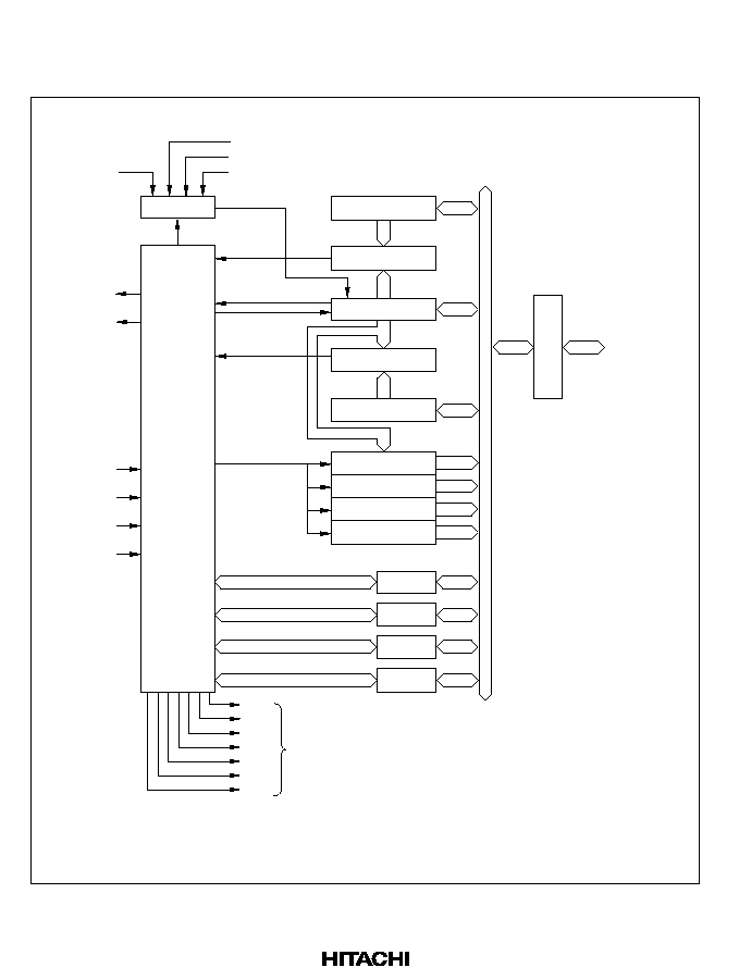
158
8.1.2
Block Diagram
Figure 8.1 shows a block diagram of the free-running timer.
External
clock source
Internal
clock sources
Clock select
Comparator A
OCRA (H/L)
Comparator B
OCRB (H/L)
Bus interface
Internal
data bus
¯
P
/2
¯
P
/8
¯
P
/32
FTCI
Compare-
match A
Clear
Clock
FTOA
FTOB
Overflow
ICRA (H/L)
Compare-
match B
Capture
FRC (H/L)
TCSR
FTIA
FTIB
FTIC
FTID
Control
logic
Module data bus
TIER
TCR
TOCR
Interrupt signals
ICIA
ICIB
ICIC
ICID
OCIA
OCIB
FOVI
Legend:
OCRA, B:
FRC:
ICRA, B, C, D:
TCSR:
Output compare register A, B (16 bits)
Free-running counter (16 bits)
Input capture register A, B, C, D (16 bits)
Timer control/status register (8 bits)
TIER:
TCR:
TOCR:
Timer interrupt enable register (8 bits)
Timer control register (8 bits)
Timer output compare control
register (8 bits)
ICRB (H/L)
ICRC (H/L)
ICRD (H/L)
Figure 8.1 Block Diagram of 16-Bit Free-Running Timer

159
8.1.3
Input and Output Pins
Table 8.1 lists the input and output pins of the free-running timer module.
Table 8.1
Input and Output Pins of Free-Running Timer Module
Name
Abbreviation
I/O
Function
Counter clock input
FTCI
Input
Input of external free-running counter
clock signal
Output compare A
FTOA
Output
Output controlled by comparator A
Output compare B
FTOB
Output
Output controlled by comparator B
Input capture A
FTIA
Input
Trigger for capturing current count into
input capture register A
Input capture B
FTIB
Input
Trigger for capturing current count into
input capture register B
Input capture C
FTIC
Input
Trigger for capturing current count into
input capture register C
Input capture D
FTID
Input
Trigger for capturing current count into
input capture register D

160
8.1.4
Register Configuration
Table 8.2 lists the registers of the free-running timer module.
Table 8.2
Register Configuration
Name
Abbreviation
R/W
Initial
Value
Address
Timer interrupt enable register
TIER
R/W
H'01
H'FF90
Timer control/status register
TCSR
R/(W)
*
1
H'00
H'FF91
Free-running counter (high)
FRC (H)
R/W
H'00
H'FF92
Free-running counter (low)
FRC (L)
R/W
H'00
H'FF93
Output compare register A/B (high)
*
2
OCRA/B (H)
R/W
H'FF
H'FF94
*
2
Output compare register A/B (low)
*
2
OCRA/B (L)
R/W
H'FF
H'FF95
*
2
Timer control register
TCR
R/W
H'00
H'FF96
Timer output compare control register
TOCR
R/W
H'E0
H'FF97
Input capture register A (high)
ICRA (H)
R
H'00
H'FF98
Input capture register A (low)
ICRA (L)
R
H'00
H'FF99
Input capture register B (high)
ICRB (H)
R
H'00
H'FF9A
Input capture register B (low)
ICRB (L)
R
H'00
H'FF9B
Input capture register C (high)
ICRC (H)
R
H'00
H'FF9C
Input capture register C (low)
ICRC (L)
R
H'00
H'FF9D
Input capture register D (high)
ICRD (H)
R
H'00
H'FF9E
Input capture register D (low)
ICRD (L)
R
H'00
H'FF9F
Notes:
*
1 Software can write a 0 to clear bits 7 to 1, but cannot write a 1 in these bits. Bit 0 can be
read and written to.
*
2 OCRA and OCRB share the same addresses. Access is controlled by the OCRS
bit in TOCR.

161
8.2
Register Descriptions
8.2.1
Free-Running Counter (FRC)
Bi t
15
14
13
12
11
10
9
8
7
6
5
4
3
2
1
0
Initial value
0
0
0
0
0
0
0
0
0
0
0
0
0
0
0
0
Read/Write
R/W R/W R/W R/W R/W R/W R/W R/W R/W R/W R/W R/W R/W R/W R/W R/W
FRC is a 16-bit readable/writable up-counter that increments on an internal pulse generated from a
clock source. The clock source is selected by the clock select 1 and 0 bits (CKS1 and CKS0) of the
timer control register (TCR).
When FRC overflows from H'FFFF to H'0000, the overflow flag (OVF) in the timer control/status
register (TCSR) is set to 1.
Because FRC is a 16-bit register, a temporary register (TEMP) is used when FRC is written or
read. See section 8.3, CPU Interface, for details.
FRC is initialized to H'0000 by a reset and in the standby modes.
8.2.2
Output Compare Registers A and B (OCRA and OCRB)
Bi t
15
14
13
12
11
10
9
8
7
6
5
4
3
2
1
0
Initial value
1
1
1
1
1
1
1
1
1
1
1
1
1
1
1
1
Read/Write
R/W R/W R/W R/W R/W R/W R/W R/W R/W R/W R/W R/W R/W R/W R/W R/W
OCRA and OCRB are 16-bit readable/writable registers, the contents of which are continually
compared with the value in the FRC. When a match is detected, the corresponding output compare
flag (OCFA or OCFB) is set in the timer control/status register (TCSR).
In addition, if the output enable bit (OEA or OEB) in the timer output compare control register
(TOCR) is set to 1, when the output compare register and FRC values match, the logic level
selected by the output level bit (OLVLA or OLVLB) in TOCR is output at the output compare pin
(FTOA or FTOB). Following a reset, the FTOA and FTOB output levels are 0 until the first
compare-match.
OCRA and OCRB share the same address. They are differentiated by the OCRS bit in TOCR. A
temporary register (TEMP) is used for write access, as explained in section 8.3, CPU Interface.
OCRA and OCRB are initialized to H'FFFF by a reset and in the standby modes.
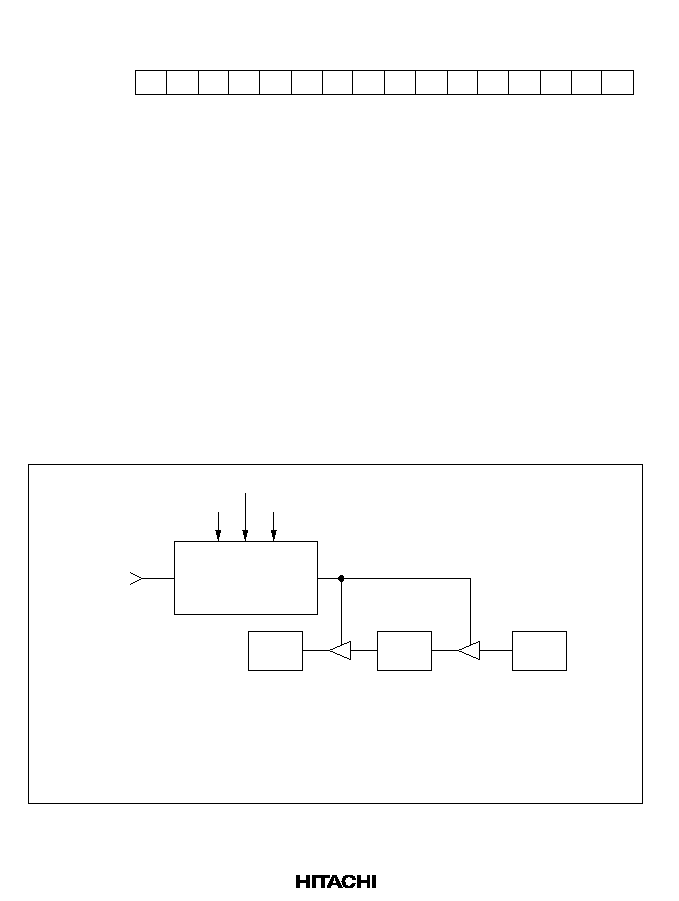
162
8.2.3
Input Capture Registers A to D (ICRA to ICRD)
Bi t
15
14
13
12
11
10
9
8
7
6
5
4
3
2
1
0
Initial value
0
0
0
0
0
0
0
0
0
0
0
0
0
0
0
0
Read/Write
R
R
R
R
R
R
R
R
R
R
R
R
R
R
R
R
There are four input capture registers A to D, each of which is a 16-bit read-only register.
When the rising or falling edge of the signal at an input capture pin (FTIA to FTID) is detected,
the current FRC value is copied to the corresponding input capture register (ICRA to ICRD).* At
the same time, the corresponding input capture flag (ICFA to ICFD) in the timer control/status
register (TCSR) is set to 1. The input capture edge is selected by the input edge select bits
(IEDGA to IEDGD) in the timer control register (TCR).
Note: * The FRC contents are transferred to the input capture register regardless of the value of the
input capture flag (ICFA/B/C/D).
Input capture can be buffered by using the input capture registers in pairs. When the BUFEA bit in
TCR is set to 1, ICRC is used as a buffer register for ICRA as shown in figure 8.2. When an FTIA
input is received, the old ICRA contents are moved into ICRC, and the new FRC count is copied
into ICRA.
BUFEA:
IEDGA:
IEDGC:
ICRC:
ICRA:
FRC:
Buffer enable A
Input edge select A
Input edge select C
Input capture register C
Input capture register A
Free-running counter
BUFEA
IEDGA
IEDGC
FTIA
Edge detect and
capture signal
generating circuit
FRC
ICRC
ICRA
Figure 8.2 Input Capture Buffering (Example)

163
Similarly, when the BUFEB bit in TCR is set to 1, ICRD is used as a buffer register for ICRB.
When input capture is buffered, if the two input edge bits are set to different values (IEDGA
IEDGC or IEDGB
IEDGD), then input capture is triggered on both the rising and falling edges
of the FTIA or FTIB input signal. If the two input edge bits are set to the same value (IEDGA =
IEDGC or IEDGB = IEDGD), then input capture is triggered on only one edge. See table 8.3.
Table 8.3
Buffered Input Capture Edge Selection (Example)
IEDGA
IEDGC
Input Capture Edge
0
0
Captured on falling edge of input capture A (FTIA)
(Initial value)
1
Captured on both rising and falling edges of input capture A (FTIA)
1
0
1
Captured on rising edge of input capture A (FTIA)
Because the input capture registers are 16-bit registers, a temporary register (TEMP) is used when
they are read. See section 8.3, CPU Interface, for details.
To ensure input capture, the width of the input capture pulse should be at least 1.5 system clock
(¯) periods. When triggering is enabled on both edges, the input capture pulse width should be at
least 2.5 system clock periods.
The input capture registers are initialized to H'0000 by a reset and in the standby modes.

164
8.2.4
Timer Interrupt Enable Register (TIER)
Bi t
7
6
5
4
3
2
1
0
ICIAE
ICIBE
ICICE
ICIDE
OCIAE
OCIBE
OVIE
--
Initial value
0
0
0
0
0
0
0
1
Read/Write
R/W
R/W
R/W
R/W
R/W
R/W
R/W
--
TIER is an 8-bit readable/writable register that enables and disables interrupts.
TIER is initialized to H'01 by a reset and in the standby modes.
Bit 7--Input Capture Interrupt A Enable (ICIAE): This bit selects whether to request input
capture interrupt A (ICIA) when input capture flag A (ICFA) in the timer status/control register
(TCSR) is set to 1.
Bit 7: ICIAE
Description
0
Input capture interrupt request A (ICIA) is disabled.
(Initial value)
1
Input capture interrupt request A (ICIA) is enabled.
Bit 6--Input Capture Interrupt B Enable (ICIBE): This bit selects whether to request input
capture interrupt B (ICIB) when input capture flag B (ICFB) in TCSR is set to 1.
Bit 6: ICIBE
Description
0
Input capture interrupt request B (ICIB) is disabled.
(Initial value)
1
Input capture interrupt request B (ICIB) is enabled.
Bit 5--Input Capture Interrupt C Enable (ICICE): This bit selects whether to request input
capture interrupt C (ICIC) when input capture flag C (ICFC) in TCSR is set to 1.
Bit 5: ICICE
Description
0
Input capture interrupt request C (ICIC) is disabled.
(Initial value)
1
Input capture interrupt request C (ICIC) is enabled.
Bit 4--Input Capture Interrupt D Enable (ICIDE): This bit selects whether to request input
capture interrupt D (ICID) when input capture flag D (ICFD) in TCSR is set to 1.
Bit 4: ICIDE
Description
0
Input capture interrupt request D (ICID) is disabled.
(Initial value)
1
Input capture interrupt request D (ICID) is enabled.

165
Bit 3--Output Compare Interrupt A Enable (OCIAE): This bit selects whether to request
output compare interrupt A (OCIA) when output compare flag A (OCFA) in TCSR is set to 1.
Bit 3: OCIAE
Description
0
Output compare interrupt request A (OCIA) is disabled.
(Initial value)
1
Output compare interrupt request A (OCIA) is enabled.
Bit 2--Output Compare Interrupt B Enable (OCIBE): This bit selects whether to request
output compare interrupt B (OCIB) when output compare flag B (OCFB) in TCSR is set to 1.
Bit 2: OCIBE
Description
0
Output compare interrupt request B (OCIB) is disabled.
(Initial value)
1
Output compare interrupt request B (OCIB) is enabled.
Bit 1--Timer Overflow Interrupt Enable (OVIE): This bit selects whether to request a free-
running timer overflow interrupt (FOVI) when the timer overflow flag (OVF) in TCSR is set to 1.
Bit 1: OVIE
Description
0
Timer overflow interrupt request (FOVI) is disabled.
(Initial value)
1
Timer overflow interrupt request (FOVI) is enabled.
Bit 0--Reserved: This bit cannot be modified and is always read as 1.

166
8.2.5
Timer Control/Status Register (TCSR)
Bi t
7
6
5
4
3
2
1
0
ICFA
ICFB
ICFC
ICFD
OCFA
OCFB
OVF
CCLRA
Initial value
0
0
0
0
0
0
0
0
Read/Write
R/(W)
*
R/(W)
*
R/(W)
*
R/(W)
*
R/(W)
*
R/(W)
*
R/(W)
*
R/W
Note:
*
Software can write a 0 in bits 7 to 1 to clear the flags, but cannot write a 1 in these bits.
TCSR is an 8-bit readable and partially writable register that contains the seven interrupt flags and
specifies whether to clear the counter on compare-match A (when the FRC and OCRA values
match).
TCSR is initialized to H'00 by a reset and in the standby modes.
Timing is described in section 8.4, Operation.
Bit 7--Input Capture Flag A (ICFA): This status bit is set to 1 to flag an input capture A event.
If BUFEA = 0, ICFA indicates that the FRC value has been copied to ICRA. If BUFEA = 1, ICFA
indicates that the old ICRA value has been moved into ICRC and the new FRC value has been
copied to ICRA.
ICFA must be cleared by software. It is set by hardware, however, and cannot be set by software.
Bit 7: ICFA
Description
0
To clear ICFA, the CPU must read ICFA after it has been set to 1, then write a
0 in this bit.
(Initial value)
1
This bit is set to 1 when an FTIA input signal causes the FRC value to be
copied to ICRA.
Bit 6--Input Capture Flag B (ICFB): This status bit is set to 1 to flag an input capture B event.
If BUFEB = 0, ICFB indicates that the FRC value has been copied to ICRB. If BUFEB = 1, ICFB
indicates that the old ICRB value has been moved into ICRD and the new FRC value has been
copied to ICRB.
ICFB must be cleared by software. It is set by hardware, however, and cannot be set by software.
Bit 6: ICFB
Description
0
To clear ICFB, the CPU must read ICFB after it has been set to 1, then write a
0 in this bit.
(Initial value)
1
This bit is set to 1 when an FTIB input signal causes the FRC value to be
copied to ICRB.

167
Bit 5--Input Capture Flag C (ICFC): This status bit is set to 1 to flag input of a rising or falling
edge of FTIC as selected by the IEDGC bit. When BUFEA = 0, this indicates capture of the FRC
count in ICRC. When BUFEA = 1, however, the FRC count is not captured, so ICFC becomes
simply an external interrupt flag. In other words, the buffer mode frees FTIC for use as a general-
purpose interrupt signal (which can be enabled or disabled by the ICICE bit).
ICFC must be cleared by software. It is set by hardware, however, and cannot be set by software.
Bit 5: ICFC
Description
0
To clear ICFC, the CPU must read ICFC after it has been set to 1, then write a
0 in this bit.
(Initial value)
1
This bit is set to 1 when an FTIC input signal is received.
Bit 4--Input Capture Flag D (ICFD): This status bit is set to 1 to flag input of a rising or falling
edge of FTID as selected by the IEDGD bit. When BUFEB = 0, this indicates capture of the FRC
count in ICRD. When BUFEB = 1, however, the FRC count is not captured, so ICFD becomes
simply an external interrupt flag. In other words, the buffer mode frees FTID for use as a general-
purpose interrupt signal (which can be enabled or disabled by the ICIDE bit).
ICFD must be cleared by software. It is set by hardware, however, and cannot be set by software.
Bit 4: ICFD
Description
0
To clear ICFD, the CPU must read ICFD after it has been set to 1, then write a
0 in this bit.
(Initial value)
1
This bit is set to 1 when an FTID input signal is received.
Bit 3--Output Compare Flag A (OCFA): This status flag is set to 1 when the FRC value
matches the OCRA value. This flag must be cleared by software. It is set by hardware, however,
and cannot be set by software.
Bit 3: OCFA
Description
0
To clear OCFA, the CPU must read OCFA after it has been set to 1, then write
a 0 in this bit.
(Initial value)
1
This bit is set to 1 when FRC = OCRA.

168
Bit 2--Output Compare Flag B (OCFB): This status flag is set to 1 when the FRC value
matches the OCRB value. This flag must be cleared by software. It is set by hardware, however,
and cannot be set by software.
Bit 2: OCFB
Description
0
To clear OCFB, the CPU must read OCFB after it has been set to 1, then write
a 0 in this bit.
(Initial value)
1
This bit is set to 1 when FRC = OCRB.
Bit 1--Timer Overflow Flag (OVF): This status flag is set to 1 when FRC overflows (changes
from H'FFFF to H'0000). This flag must be cleared by software. It is set by hardware, however,
and cannot be set by software.
Bit 1: OVF
Description
0
To clear OVF, the CPU must read OVF after it has been set to 1, then write a 0
in this bit.
(Initial value)
1
This bit is set to 1 when FRC changes from H'FFFF to H'0000.
Bit 0--Counter Clear A (CCLRA): This bit selects whether to clear FRC at compare-match A
(when the FRC and OCRA values match).
Bit 0: CCLRA
Description
0
The FRC is not cleared.
(Initial value)
1
The FRC is cleared at compare-match A.
8.2.6
Timer Control Register (TCR)
Bi t
7
6
5
4
3
2
1
0
IEDGA
IEDGB
IEDGC
IEDGD
BUFEA
BUFEB
CKS1
CKS0
Initial value
0
0
0
0
0
0
0
0
Read/Write
R/W
R/W
R/W
R/W
R/W
R/W
R/W
R/W
TCR is an 8-bit readable/writable register that selects the rising or falling edge of the input capture
signals, enables the input capture buffer mode, and selects the FRC clock source.
TCR is initialized to H'00 by a reset and in the standby modes.

169
Bit 7--Input Edge Select A (IEDGA): This bit selects the rising or falling edge of the input
capture A signal (FTIA).
Bit 7: IEDGA
Description
0
Input capture A events are recognized on the falling edge of FTIA. (Initial value)
1
Input capture A events are recognized on the rising edge of FTIA.
Bit 6--Input Edge Select B (IEDGB): This bit selects the rising or falling edge of the input
capture B signal (FTIB).
Bit 6: IEDGB
Description
0
Input capture B events are recognized on the falling edge of FTIB. (Initial value)
1
Input capture B events are recognized on the rising edge of FTIB.
Bit 5--Input Edge Select C (IEDGC): This bit selects the rising or falling edge of the input
capture C signal (FTIC).
Bit 5: IEDGC
Description
0
Input capture C events are recognized on the falling edge of FTIC. (Initial value)
1
Input capture C events are recognized on the rising edge of FTIC.
Bit 4--Input Edge Select D (IEDGD): This bit selects the rising or falling edge of the input
capture D signal (FTID).
Bit 4: IEDGD
Description
0
Input capture D events are recognized on the falling edge of FTID. (Initial value)
1
Input capture D events are recognized on the rising edge of FTID.
Bit 3--Buffer Enable A (BUFEA): This bit selects whether to use ICRC as a buffer register for
ICRA.
Bit 3: BUFEA
Description
0
ICRC is used for input capture C.
(Initial value)
1
ICRC is used as a buffer register for input capture A.

170
Bit 2--Buffer Enable B (BUFEB): This bit selects whether to use ICRD as a buffer register for
ICRB.
Bit 2: BUFEB
Description
0
ICRD is used for input capture D.
(Initial value)
1
ICRD is used as a buffer register for input capture B.
Bits 1 and 0--Clock Select (CKS1 and CKS0): These bits select external clock input or one of
three internal clock sources for FRC. External clock pulses are counted on the rising edge of
signals input to pin FTCI.
Bit 1: CKS1
Bit 0: CKS0
Description
0
0
¯
P
/2 internal clock source
(Initial value)
1
¯
P
/8 internal clock source
1
0
¯
P
/32 internal clock source
1
External clock source (rising edge)
8.2.7
Timer Output Compare Control Register (TOCR)
Bi t
7
6
5
4
3
2
1
0
--
--
--
OCRS
OEA
OEB
OLVLA
OLVLB
Initial value
1
1
1
0
0
0
0
0
Read/Write
--
--
--
R/W
R/W
R/W
R/W
R/W
TOCR is an 8-bit readable/writable register that enables output from the output compare pins,
selects the output levels, and switches access between output compare registers A and B.
TOCR is initialized to H'E0 by a reset and in the standby modes.
Bits 7 to 5--Reserved: These bits cannot be modified and are always read as 1.
Bit 4--Output Compare Register Select (OCRS): OCRA and OCRB share the same address.
When this address is accessed, the OCRS bit selects which register is accessed. This bit does not
affect the operation of OCRA or OCRB.
Bit 4: OCRS
Description
0
OCRA is selected.
(Initial value)
1
OCRB is selected.

171
Bit 3--Output Enable A (OEA): This bit enables or disables output of the output compare A
signal (FTOA).
Bit 3: OEA
Description
0
Output compare A output is disabled.
(Initial value)
1
Output compare A output is enabled.
Bit 2--Output Enable B (OEB): This bit enables or disables output of the output compare B
signal (FTOB).
Bit 2: OEB
Description
0
Output compare B output is disabled.
(Initial value)
1
Output compare B output is enabled.
Bit 1--Output Level A (OLVLA): This bit selects the logic level to be output at the FTOA pin
when the FRC and OCRA values match.
Bit 1: OLVLA
Description
0
A 0 logic level is output for compare-match A.
(Initial value)
1
A 1 logic level is output for compare-match A.
Bit 0--Output Level B (OLVLB): This bit selects the logic level to be output at the FTOB pin
when the FRC and OCRB values match.
Bit 0: OLVLB
Description
0
A 0 logic level is output for compare-match B.
(Initial value)
1
A 1 logic level is output for compare-match B.

172
8.3
CPU Interface
The free-running counter (FRC), output compare registers (OCRA and OCRB), and input capture
registers (ICRA to ICRD) are 16-bit registers, but they are connected to an 8-bit data bus. When
the CPU accesses these registers, to ensure that both bytes are written or read simultaneously, the
access is performed using an 8-bit temporary register (TEMP).
These registers are written and read as follows:
∑
Register Write
When the CPU writes to the upper byte, the byte of write data is placed in TEMP. Next, when
the CPU writes to the lower byte, this byte of data is combined with the byte in TEMP and all
16 bits are written in the register simultaneously.
∑
Register Read
When the CPU reads the upper byte, the upper byte of data is sent to the CPU and the lower
byte is placed in TEMP. When the CPU reads the lower byte, it receives the value in TEMP.
Programs that access these registers should normally use word access. Equivalently, they may
access first the upper byte, then the lower byte by two consecutive byte accesses. Data will not be
transferred correctly if the bytes are accessed in reverse order, or if only one byte is accessed.
Figure 8.3 shows the data flow when FRC is accessed. The other registers are accessed in the same
way. As an exception, when the CPU reads OCRA or OCRB, it reads both the upper and lower
bytes directly, without using TEMP.
Coding Examples
To write the contents of general register R0 to OCRA:
MOV.W R0, @OCRA
To transfer the contents of ICRA to general register R0:
MOV.W @ICRA, R0
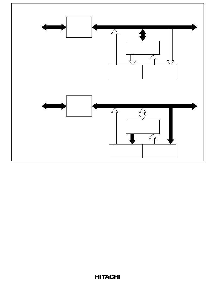
173
CPU writes
data H'AA
(1) Upper byte write
(2) Lower byte write
CPU writes
data H'55
Bus
interface
Bus
interface
Module data bus
Module data bus
TEMP
[H'AA]
FRCH
[ ]
FRCL
[ ]
TEMP
[H'AA]
FRCH
[H'AA]
FRCL
[H'55]
Figure 8.3 (a) Write Access to FRC (when CPU Writes H'AA55)

174
CPU reads
data H'AA
(1) Upper byte read
(2) Lower byte read
CPU reads
data H'55
Bus
interface
Bus
interface
Module data bus
Module data bus
TEMP
[H'55]
FRCH
[H'AA]
FRCL
[H'55]
TEMP
[H'55]
FRCH
[ ]
FRCL
[ ]
Figure 8.3 (b) Read Access to FRC (when FRC Contains H'AA55)

175
8.4
Operation
8.4.1
FRC Increment Timing
FRC increments on a pulse generated once for each period of the selected (internal or external)
clock source. The clock source is selected by bits CKS0 and CKS1 in TCR.
Internal Clock: The internal clock sources (¯
P
/2, ¯
P
/8, ¯
P
/32) are created from the system clock
(¯) by a prescaler. FRC increments on a pulse generated from the falling edge of the prescaler
output. See figure 8.4.
N ≠ 1
FRC clock
pulse
¯
FRC
Internal
clock
N
N + 1
Figure 8.4 Increment Timing for Internal Clock Source
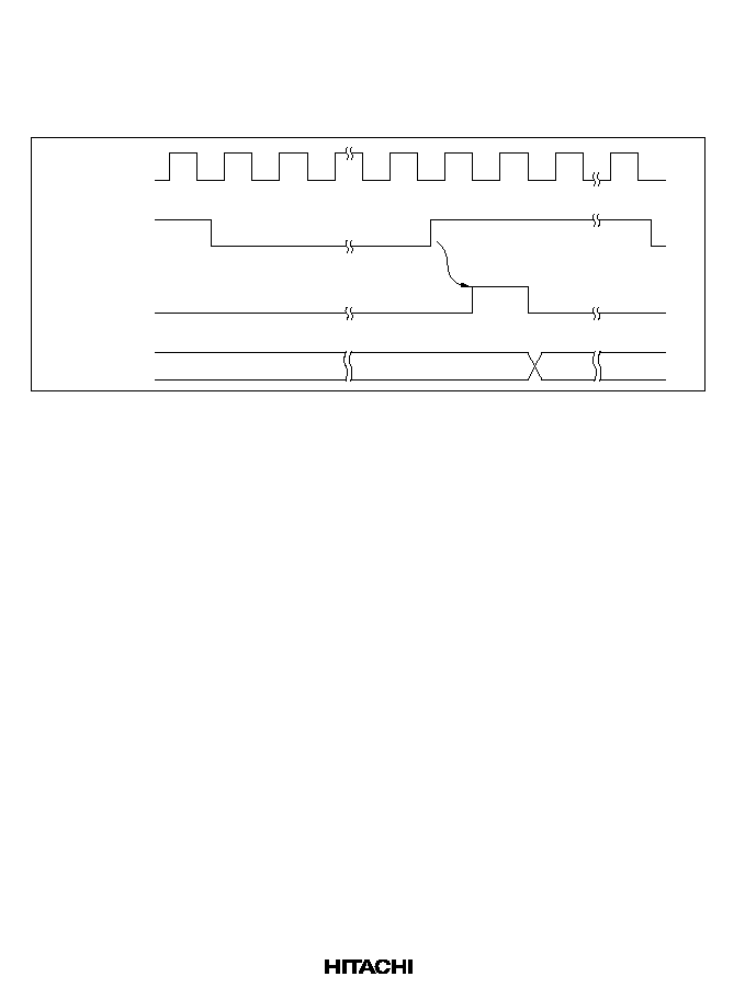
176
External Clock: If external clock input is selected, FRC increments on the rising edge of the
FTCI clock signal. Figure 8.5 shows the increment timing.
The pulse width of the external clock signal must be at least 1.5 system clock (¯) periods. The
counter will not increment correctly if the pulse width is shorter than 1.5 system clock periods.
N + 1
N
FRC clock
pulse
¯
FRC
FTCI
Figure 8.5 Increment Timing for External Clock Source

177
8.4.2
Output Compare Timing
When a compare-match occurs, the logic level selected by the output level bit (OLVLA or
OLVLB) in TOCR is output at the output compare pin (FTOA or FTOB). Figure 8.6 shows the
timing of this operation for compare-match A.
N + 1
N
N + 1
N
N
OCRA
¯
Internal compare-
match A signal
FRC
OLVLA
FTOA
Clear
*
Note:
*
Cleared by software
N
Figure 8.6 Timing of Output Compare A
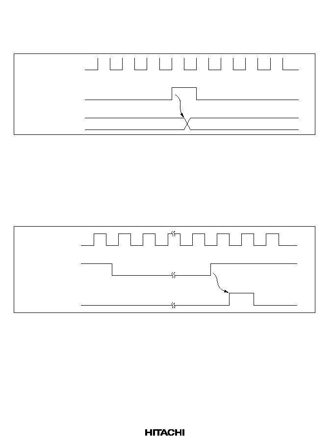
178
8.4.3
FRC Clear Timing
If the CCLRA bit in TCSR is set to 1, the FRC is cleared when compare-match A occurs. Figure
8.7 shows the timing of this operation.
N
H'0000
FRC
¯
Internal compare-
match A signal
Figure 8.7 Clearing of FRC by Compare-Match A
8.4.4
Input Capture Timing
Input Capture Timing: An internal input capture signal is generated from the rising or falling
edge of the signal at the input capture pin FTIx (x = A, B, C, D), as selected by the corresponding
IEDGx bit in TCR. Figure 8.8 shows the usual input capture timing when the rising edge is
selected (IEDGx = 1).
Internal input
capture signal
¯
Input data
FTI pin
Figure 8.8 Input Capture Timing (Usual Case)
If the upper byte of ICRA/B/C/D is being read when the corresponding input capture signal
arrives, the internal input capture signal is delayed by one state. Figure 8.9 shows the timing for
this case.

179
Internal input
capture signal
¯
Input at FTI pin
T
1
T
2
T
3
ICR upper byte read cycle
Figure 8.9 Input Capture Timing (1-State Delay Due to ICRA/B/C/D Read)
Buffered Input Capture Timing: ICRC and ICRD can operate as buffers for ICRA and ICRB.
Figure 8.10 shows how input capture operates when ICRA and ICRC are used in buffer mode and
IEDGA and IEDGC are set to different values (IEDGA = 0 and IEDGC = 1, or IEDG A = 1 and
IEDGC = 0), so that input capture is performed on both the rising and falling edges of FTIA.
n
n + 1
N
N + 1
M
n
n
N
m
M
M
n
¯
FTIA
Internal input
capture signal
FRC
ICRA
ICRC
Figure 8.10 Buffered Input Capture with Both Edges Selected
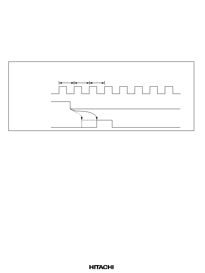
180
When ICRC or ICRD is used as a buffer register, its input capture flag is set by the selected
transition of its input capture signal. For example, if ICRC is used to buffer ICRA, when the edge
transition selected by the IEDGC bit occurs on the FTIC input capture line, ICFC will be set, and
if the ICIEC bit is set, an interrupt will be requested. The FRC value will not be transferred to
ICRC, however.
In buffered input capture, if the upper byte of either of the two registers to which data will be
transferred (ICRA and ICRC, or ICRB and ICRD) is being read when the input signal arrives,
input capture is delayed by one system clock (¯). Figure 8.11 shows the timing when BUFEA = 1.
Internal input
capture signal
¯
Input at
FTIA pin
T
1
T
2
T
3
Read cycle:
CPU reads upper byte of ICRA or ICRC
Figure 8.11 Input Capture Timing (1-State Delay, Buffer Mode)
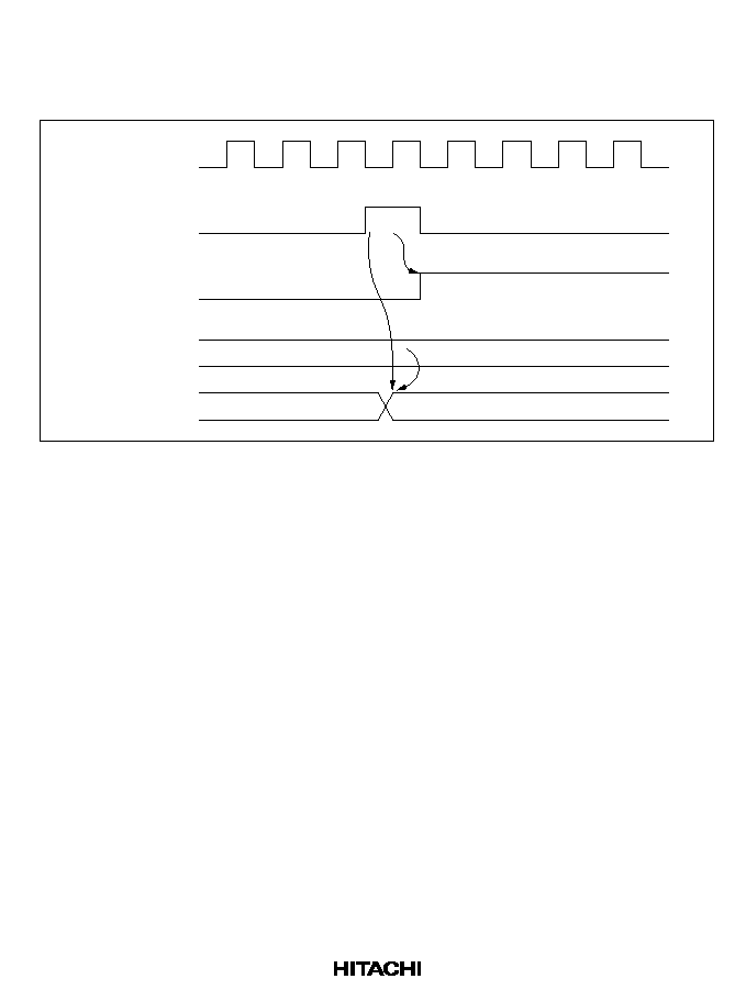
181
8.4.5
Timing of Input Capture Flag (ICF) Setting
The input capture flag ICFx (x = A, B, C, D) is set to 1 by the internal input capture signal. Figure
8.12 shows the timing of this operation.
ICF
¯
FRC
Internal input
capture signal
N
N
ICR
Figure 8.12 Setting of Input Capture Flag
8.4.6
Setting of Output Compare Flags A and B (OCFA and OCFB)
The output compare flags are set to 1 by an internal compare-match signal generated when the
FRC value matches the OCRA or OCRB value. This compare-match signal is generated at the last
state in which the two values match, just before FRC increments to a new value.
Accordingly, when the FRC and OCR values match, the compare-match signal is not generated
until the next period of the clock source. Figure 8.13 shows the timing of the setting of the output
compare flags.

182
OCRA or OCRB
¯
Internal compare-
match signal
FRC
N
N + 1
N
OCFA or OCFB
Figure 8.13 Setting of Output Compare Flags
8.4.7
Setting of Timer Overflow Flag (OVF)
The timer overflow flag (OVF) is set to 1 when FRC overflows (changes from H'FFFF to H'0000).
Figure 8.14 shows the timing of this operation.
H'FFFF
H'0000
Internal overflow
signal
¯
FRC
OVF
Figure 8.14 Setting of Timer Overflow Flag (OVF)

183
8.5
Interrupts
The free-running timer can request seven interrupts (three types): input capture A to D (ICIA,
ICIB, ICIC, ICID), output compare A and B (OCIA and OCIB), and overflow (FOVI). Each
interrupt can be enabled or disabled by an enable bit in TIER. Independent signals are sent to the
interrupt controller for each interrupt. Table 8.4 lists information about these interrupts.
Table 8.4
Free-Running Timer Interrupts
Interrupt
Description
Priority
ICIA
Requested by ICFA
High
ICIB
Requested by ICFB
ICIC
Requested by ICFC
ICID
Requested by ICFD
OCIA
Requested by OCFA
OCIB
Requested by OCFB
FOVI
Requested by OVF
Low

184
8.6
Sample Application
In the example below, the free-running timer is used to generate two square-wave outputs with a
50% duty cycle and arbitrary phase relationship. The programming is as follows:
1. The CCLRA bit in TCSR is set to 1.
2. Each time a compare-match interrupt occurs, software inverts the corresponding output level
bit in TOCR (OLVLA or OLVLB).
T
1
T
2
T
3
Write cycle:
CPU write to lower byte of FRC
Internal address
bus
FRC address
Internal write
signal
¯
FRC clear signal
FRC
N
H'0000
Figure 8.15 Square-Wave Output (Example)
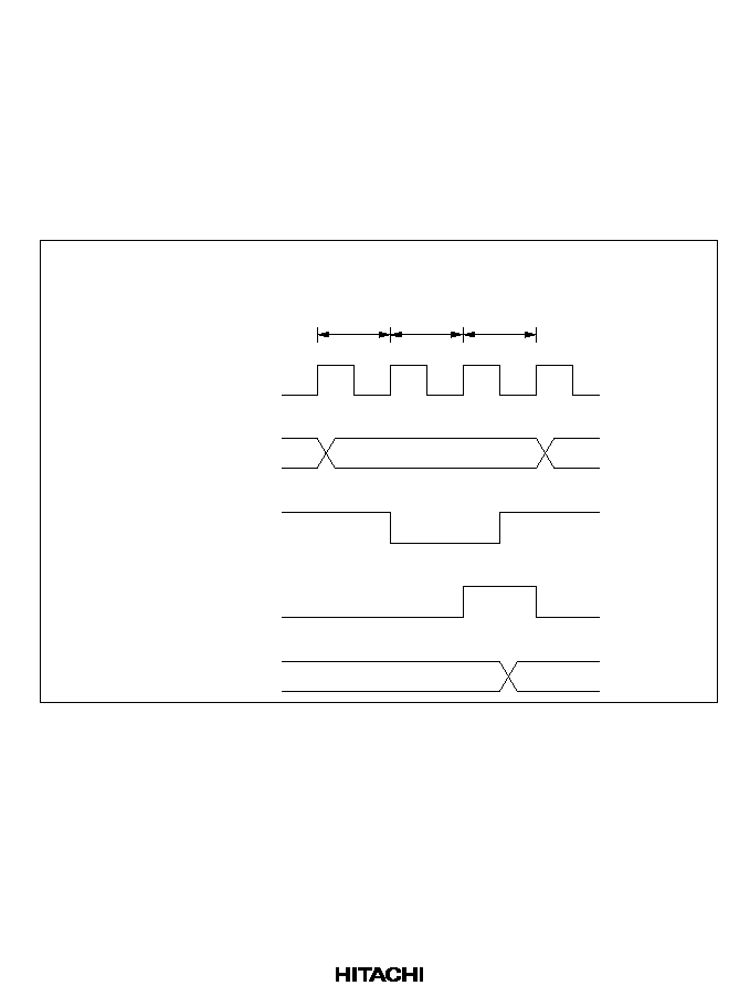
185
8.7
Application Notes
Application programmers should note that the following types of contention can occur in the free-
running timer.
Contention between FRC Write and Clear: If an internal counter clear signal is generated
during the T
3
state of a write cycle to the lower byte of the free-running counter, the clear signal
takes priority and the write is not performed.
Figure 8.16 shows this type of contention.
T
1
T
2
T
3
Write cycle:
CPU write to lower byte of FRC
Internal address
bus
FRC address
Internal write
signal
¯
FRC clear signal
FRC
N
H'0000
Figure 8.16 FRC Write-Clear Contention
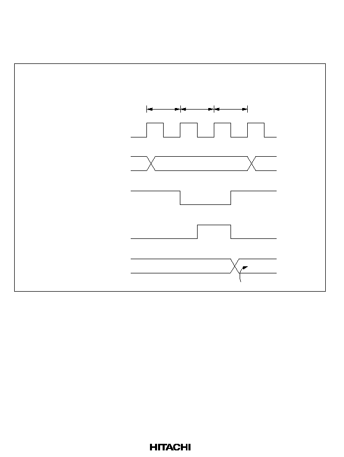
186
Contention between FRC Write and Increment: If an FRC increment pulse is generated during
the T
3
state of a write cycle to the lower byte of the free-running counter, the write takes priority
and FRC is not incremented.
Figure 8.17 shows this type of contention.
T
1
T
2
T
3
Write cycle:
CPU write to lower byte of FRC
Internal address bus
Internal write signal
¯
FRC clock pulse
FRC
N
M
Write data
FRC address
Figure 8.17 FRC Write-Increment Contention
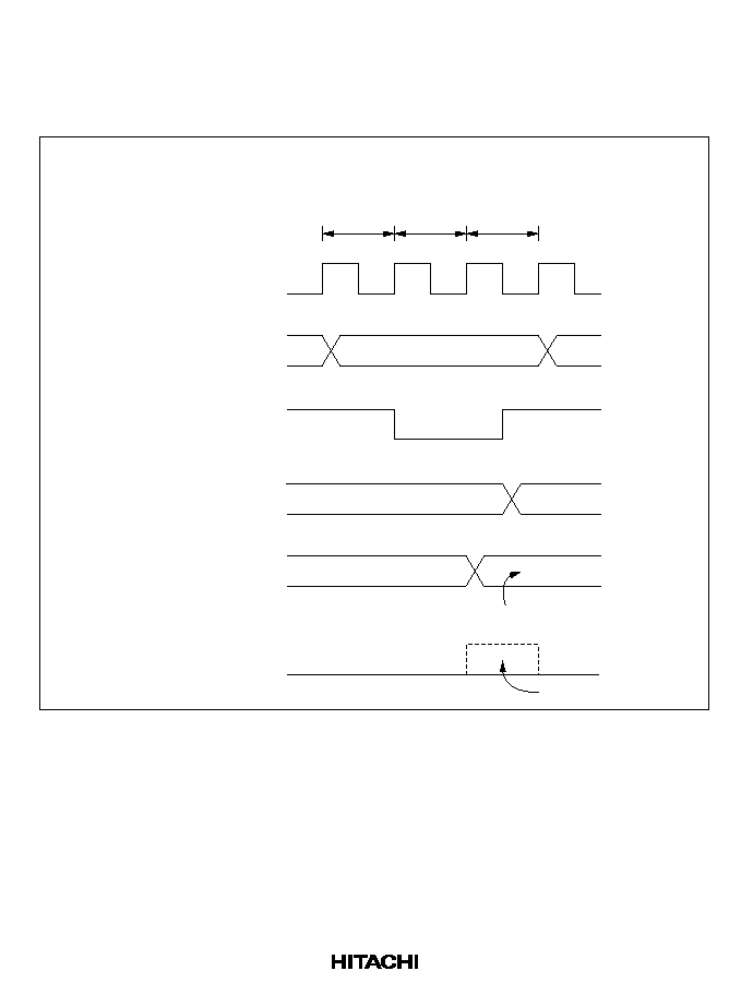
187
Contention between OCR Write and Compare-Match: If a compare-match occurs during the
T
3
state of a write cycle to the lower byte of OCRA or OCRB, the write takes priority and the
compare-match signal is inhibited.
Figure 8.18 shows this type of contention.
T
1
T
2
T
3
Write cycle:
CPU write to lower byte of OCRA or OCRB
Internal address bus
Internal write signal
¯
FRC
OCRA or OCRB
N
M
Write data
OCR address
N
N + 1
Compare-match
A or B signal
Inhibited
Figure 8.18 Contention between OCR Write and Compare-Match
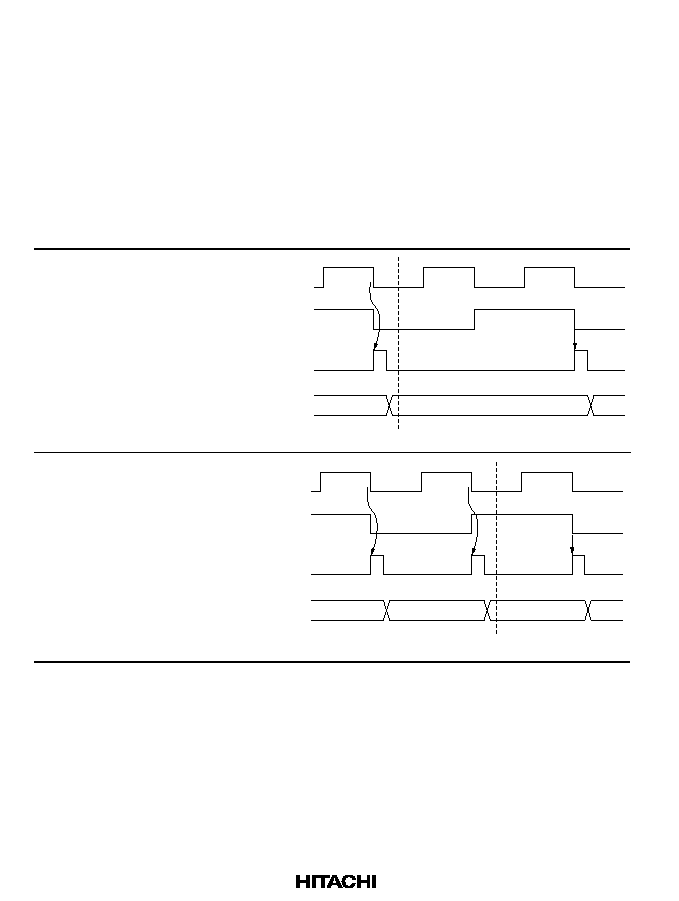
188
Increment Caused by Changing of Internal Clock Source: When an internal clock source is
changed, the changeover may cause FRC to increment. This depends on the time at which the
clock select bits (CKS1 and CKS0) are rewritten, as shown in table 8.5.
The pulse that increments FRC is generated at the falling edge of the internal clock source. If
clock sources are changed when the old source is high and the new source is low, as in case no. 3
in table 8.5, the changeover generates a falling edge that triggers the FRC increment clock pulse.
Switching between an internal and external clock source can also cause FRC to increment.
Table 8.5
Effect of Changing Internal Clock Sources
No.
Description
Timing
1
Low
low:
CKS1 and CKS0 are
rewritten while both
clock sources are low.
N + 1
Old clock
source
New clock
source
FRC clock
pulse
FRC
CKS rewrite
N
2
Low
high:
CKS1 and CKS0 are
rewritten while old
clock source is low and
new clock source is high.
N + 1
N + 2
Old clock
source
New clock
source
FRC clock
pulse
FRC
CKS rewrite
N
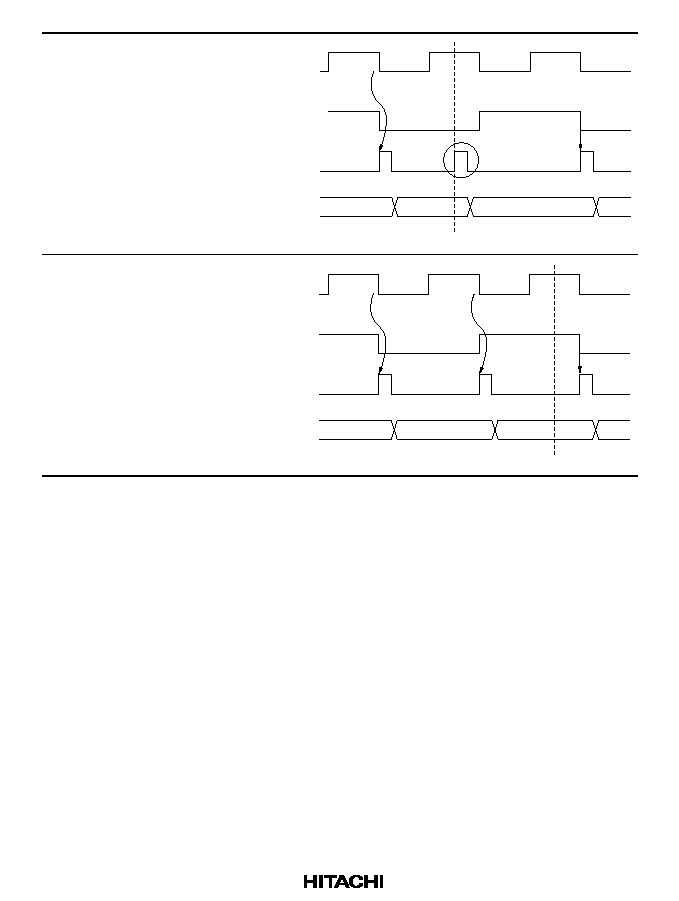
189
No.
Description
Timing
3
High
low:
CKS1 and CKS0 are
rewritten while old clock
source is high and new
clock source is low.
N + 1
N
N + 2
*
Old clock
source
New clock
source
FRC clock
pulse
FRC
CKS rewrite
4
High
high:
CKS1 and CKS0 are
rewritten while both
clock sources are high.
N + 1
N + 2
N
Old clock
source
New clock
source
FRC clock
pulse
CKS rewrite
FRC
Note:
*
The switching of clock sources is regarded as a falling edge that increments FRC.

190

191
Section 9 8-Bit Timers
9.1
Overview
The H8/3337 Series and H8/3397 Series include an 8-bit timer module with two channels
(numbered 0 and 1). Each channel has an 8-bit counter (TCNT) and two time constant registers
(TCORA and TCORB) that are constantly compared with the TCNT value to detect compare-
match events. One of the many applications of the 8-bit timer module is to generate a rectangular-
wave output with an arbitrary duty cycle.
9.1.1
Features
The features of the 8-bit timer module are listed below.
∑
Selection of seven clock sources
The counters can be driven by one of six internal clock signals or an external clock input
(enabling use as an external event counter).
∑
Selection of three ways to clear the counters
The counters can be cleared on compare-match A or B, or by an external reset signal.
∑
Timer output controlled by two compare-match signals
The timer output signal in each channel is controlled by two independent compare-match
signals, enabling the timer to generate output waveforms with an arbitrary duty cycle, or PWM
waveforms.
∑
Three independent interrupts
Compare-match A and B and overflow interrupts can be requested independently.

192
9.1.2
Block Diagram
Figure 9.1 shows a block diagram of one channel in the 8-bit timer module.
External
clock source
TMCI
TMO
TMRI
Internal
clock sources
Channel 0
Channel 1
¯
P
/2
¯
P
/8
¯
P
/32
¯
P
/64
¯
P
/256
¯
P
/1024
¯
P
/2
¯
P
/8
¯
P
/64
¯
P
/128
¯
P
/1024
¯
P
/2048
Clock
Overflow
Clear
Compare-match B
Control
logic
Clock select
TCORA
Comparator A
TCNT
Comparator B
TCORB
TCSR
TCR
Module data bus
Bus interface
Internal
data bus
CMIA
CMIB
OVI
Interrupt signals
TCORA:
TCORB:
TCNT:
TCSR:
TCR:
Time constant register A (8 bits)
Time constant register B (8 bits)
Timer counter
Timer control status register (8 bits)
Timer control register (8 bits)
Compare-match A
Figure 9.1 Block Diagram of 8-Bit Timer (1 Channel)

193
9.1.3
Input and Output Pins
Table 9.1 lists the input and output pins of the 8-bit timer.
Table 9.1
Input and Output Pins of 8-Bit Timer
Abbreviation
*
Name
Channel 0
Channel 1
I/O
Function
Timer output
TMO
0
TMO
1
Output
Output controlled by compare-match
Timer clock input
TMCI
0
TMCI
1
Input
External clock source for the counter
Timer reset input
TMRI
0
TMRI
1
Input
External reset signal for the counter
Note:
*
In this manual, the channel subscript has been deleted, and only TMO, TMCI, and TMRI
are used.
9.1.4
Register Configuration
Table 9.2 lists the registers of the 8-bit timer module.
Table 9.2
8-Bit Timer Registers
Channel
Name
Abbreviation
R/W
Initial Value
Address
0
Timer control register
TCR
R/W
H'00
H'FFC8
Timer control/status register
TCSR
R/(W)
*
H'10
H'FFC9
Time constant register A
TCORA
R/W
H'FF
H'FFCA
Time constant register B
TCORB
R/W
H'FF
H'FFCB
Timer counter
TCNT
R/W
H'00
H'FFCC
1
Timer control register
TCR
R/W
H'00
H'FFD0
Timer control/status register
TCSR
R/(W)
*
H'10
H'FFD1
Time constant register A
TCORA
R/W
H'FF
H'FFD2
Time constant register B
TCORB
R/W
H'FF
H'FFD3
Timer counter
TCNT
R/W
H'00
H'FFD4
0, 1
Serial/timer control register
STCR
R/W
H'00
H'FFC3
Note:
*
Software can write a 0 to clear bits 7 to 5, but cannot write a 1 in these bits.

194
9.2
Register Descriptions
9.2.1
Timer Counter (TCNT)
Bit
7
6
5
4
3
2
1
0
Initial value
0
0
0
0
0
0
0
0
Read/Write
R/W
R/W
R/W
R/W
R/W
R/W
R/W
R/W
Each timer counter (TCNT) is an 8-bit up-counter that increments on a pulse generated from an
internal or external clock source selected by clock select bits 2 to 0 (CKS2 to CKS0) of the timer
control register (TCR). The CPU can always read or write the timer counter.
The timer counter can be cleared by an external reset input or by an internal compare-match signal
generated at a compare-match event. Clock clear bits 1 and 0 (CCLR1 and CCLR0) of the timer
control register select the method of clearing.
When a timer counter overflows from H'FF to H'00, the overflow flag (OVF) in the timer
control/status register (TCSR) is set to 1.
The timer counters are initialized to H'00 by a reset and in the standby modes.
9.2.2
Time Constant Registers A and B (TCORA and TCORB)
Bit
7
6
5
4
3
2
1
0
Initial value
1
1
1
1
1
1
1
1
Read/Write
R/W
R/W
R/W
R/W
R/W
R/W
R/W
R/W
TCORA and TCORB are 8-bit readable/writable registers. The timer count is continually
compared with the constants written in these registers (except during the T
3
state of a write cycle
to TCORA or TCORB). When a match is detected, the corresponding compare-match flag (CMFA
or CMFB) is set in the timer control/status register (TCSR).
The timer output signal is controlled by these compare-match signals as specified by output select
bits 3 to 0 (OS3 to OS0) in the timer control/status register (TCSR).
TCORA and TCORB are initialized to H'FF by a reset and in the standby modes.

195
9.2.3
Timer Control Register (TCR)
Bit
7
6
5
4
3
2
1
0
CMIEB
CMIEA
OVIE
CCLR1
CCLR0
CKS2
CKS1
CKS0
Initial value
0
0
0
0
0
0
0
0
Read/Write
R/W
R/W
R/W
R/W
R/W
R/W
R/W
R/W
TCR is an 8-bit readable/writable register that selects the clock source and the time at which the
timer counter is cleared, and enables interrupts.
TCR is initialized to H'00 by a reset and in the standby modes.
For timing diagrams, see section 9.3, Operation.
Bit 7--Compare-Match Interrupt Enable B (CMIEB): This bit selects whether to request
compare-match interrupt B (CMIB) when compare-match flag B (CMFB) in the timer
control/status register (TCSR) is set to 1.
Bit 7: CMIEB
Description
0
Compare-match interrupt request B (CMIB) is disabled.
(Initial value)
1
Compare-match interrupt request B (CMIB) is enabled.
Bit 6--Compare-Match Interrupt Enable A (CMIEA): This bit selects whether to request
compare-match interrupt A (CMIA) when compare-match flag A (CMFA) in TCSR is set to 1.
Bit 6: CMIEA
Description
0
Compare-match interrupt request A (CMIA) is disabled.
(Initial value)
1
Compare-match interrupt request A (CMIA) is enabled.

196
Bit 5--Timer Overflow Interrupt Enable (OVIE): This bit selects whether to request a timer
overflow interrupt (OVI) when the overflow flag (OVF) in TCSR is set to 1.
Bit 5: OVIE
Description
0
The timer overflow interrupt request (OVI) is disabled.
(Initial value)
1
The timer overflow interrupt request (OVI) is enabled.
Bits 4 and 3--Counter Clear 1 and 0 (CCLR1 and CCLR0): These bits select how the timer
counter is cleared: by compare-match A or B or by an external reset input (TMRI).
Bit 4: CCLR1
Bit 3: CCLR0
Description
0
0
Not cleared.
(Initial value)
1
Cleared on compare-match A.
1
0
Cleared on compare-match B.
1
Cleared on rising edge of external reset input signal.

197
Bits 2, 1, and 0--Clock Select (CKS2, CKS1, and CKS0): These bits and bits ICKS1 and
ICKS0 in the serial/timer control register (STCR) select the internal or external clock source for
the timer counter. Six internal clock sources, derived by prescaling the system clock, are available
for each timer channel. For internal clock sources the counter is incremented on the falling edge of
the internal clock. For an external clock source, these bits can select whether to increment the
counter on the rising or falling edge of the clock input (TMCI), or on both edges.
TCR
STCR
Channel
Bit 2:
CKS2
Bit 1:
CKS1
Bit 0:
CKS0
Bit 1:
ICKS1
Bit 0:
ICKS0 Description
0
0
0
0
--
--
No clock source (timer stopped) (Initial value)
1
0
¯
P
/8 internal clock, counted on falling edge
1
¯
P
/2 internal clock, counted on falling edge
1
0
0
¯
P
/64 internal clock, counted on falling edge
1
¯
P
/32 internal clock, counted on falling edge
1
0
¯
P
/1024 internal clock, counted on falling edge
1
¯
P
/256 internal clock, counted on falling edge
1
0
0
--
No clock source (timer stopped)
1
External clock source, counted on rising edge
1
0
External clock source, counted on falling edge
1
External clock source, counted on both rising
and falling edges
1
0
0
0
--
--
No clock source (timer stopped) (Initial value)
1
0
¯
P
/8 internal clock, counted on falling edge
1
¯
P
/2 internal clock, counted on falling edge
1
0
0
¯
P
/64 internal clock, counted on falling edge
1
¯
P
/128 internal clock, counted on falling edge
1
0
¯
P
/1024 internal clock, counted on falling edge
1
¯
P
/2048 internal clock, counted on falling edge
1
0
0
--
No clock source (timer stopped)
1
External clock source, counted on rising edge
1
0
External clock source, counted on falling edge
1
External clock source, counted on both rising
and falling edges

198
9.2.4
Timer Control/Status Register (TCSR)
Bit
7
6
5
4
3
2
1
0
CMFB
CMFA
OVF
--
OS3
OS2
OS1
OS0
Initial value
0
0
0
1
0
0
0
0
Read/Write
R/(W)
*
R/(W)
*
R/(W)
*
--
R/W
R/W
R/W
R/W
Note:
*
Software can write a 0 in bits 7 to 5 to clear the flags, but cannot write a 1 in these bits.
TCSR is an 8-bit readable and partially writable register that indicates compare-match and
overflow status and selects the effect of compare-match events on the timer output signal.
TCSR is initialized to H'10 by a reset and in the standby modes.
Bit 7--Compare-Match Flag B (CMFB): This status flag is set to 1 when the timer count
matches the time constant set in TCORB. CMFB must be cleared by software. It is set by
hardware, however, and cannot be set by software.
Bit 7: CMFB
Description
0
To clear CMFB, the CPU must read CMFB after it has been set to 1, then write
a 0 in this bit.
(Initial value)
1
This bit is set to 1 when TCNT = TCORB.
Bit 6--Compare-Match Flag A (CMFA): This status flag is set to 1 when the timer count
matches the time constant set in TCORA. CMFA must be cleared by software. It is set by
hardware, however, and cannot be set by software.
Bit 6: CMFA
Description
0
To clear CMFA, the CPU must read CMFA after it has been set to 1, then write
a 0 in this bit.
(Initial value)
1
This bit is set to 1 when TCNT = TCORA.
Bit 5--Timer Overflow Flag (OVF): This status flag is set to 1 when the timer count overflows
(changes from H'FF to H'00). OVF must be cleared by software. It is set by hardware, however,
and cannot be set by software.
Bit 5: OVF
Description
0
To clear OVF, the CPU must read OVF after it has been set to 1, then write a 0
in this bit.
(Initial value)
1
This bit is set to 1 when TCNT changes from H'FF to H'00.

199
Bit 4--Reserved: This bit is always read as 1. It cannot be written.
Bits 3 to 0--Output Select 3 to 0 (OS3 to OS0): These bits specify the effect of TCOR≠TCNT
compare-match events on the timer output signal (TMO). Bits OS3 and OS2 control the effect of
compare-match B on the output level. Bits OS1 and OS0 control the effect of compare-match A on
the output level.
If compare-match A and B occur simultaneously, any conflict is resolved according to the
following priority order: toggle > 1 output > 0 output.
When all four output select bits are cleared to 0 the timer output signal is disabled.
After a reset, the timer output is 0 until the first compare-match event.
Bit 3: OS3
Bit 2: OS2
Description
0
0
No change when compare-match B occurs.
(Initial value)
1
Output changes to 0 when compare-match B occurs.
1
0
Output changes to 1 when compare-match B occurs.
1
Output inverts (toggles) when compare-match B occurs.
Bit 1: OS3
Bit 0: OS2
Description
0
0
No change when compare-match A occurs.
(Initial value)
1
Output changes to 0 when compare-match A occurs.
1
0
Output changes to 1 when compare-match A occurs.
1
Output inverts (toggles) when compare-match A occurs.

200
9.2.5
Serial/Timer Control Register (STCR)
Bit
7
6
5
4
3
2
1
0
IICS
IICD
IICX
IICE
STAC
MPE
ICKS1
ICKS0
Initial value
0
0
0
0
0
0
0
0
Read/Write
R/W
R/W
R/W
R/W
R/W
R/W
R/W
R/W
STCR is an 8-bit readable/writable register that controls the I
2
C bus interface and host interface,
controls the operating mode of the serial communication interface, and selects internal clock
sources for the timer counters.
STCR is initialized to H'00 by a reset.
Bits 7 to 4--I
2
C Control (IICS, IICD, IICX, IICE): These bits control operation of the I
2
C bus
interface. For details, see section 13, I
2
C Bus Interface.
Bit 3--Slave Input Switch (STAC): Controls the switching of the host interface input pins. For
details, see section 14, Host Interface.
Bit 2--Multiprocessor Enable (MPE): Controls the operating mode of serial communication
interfaces 0 and 1. For details, see section 12, Serial Communication Interface.
Bits 1 and 0--Internal Clock Source Select 1 and 0 (ICKS1 and ICKS0): These bits and bits
CKS2 to CKS0 in TCR select clock sources for the timer counters. For details, see section 9.2.3,
Timer Control Register.
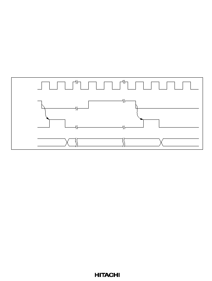
201
9.3
Operation
9.3.1
TCNT Increment Timing
The timer counter increments on a pulse generated once for each period of the selected (internal or
external) clock source.
Internal Clock: Internal clock sources are created from the system clock by a prescaler. The
counter increments on an internal TCNT clock pulse generated from the falling edge of the
prescaler output, as shown in figure 9.2. Bits CKS2 to CKS0 of TCR and bits ICKS1 and ICKS0
of STCR can select one of the six internal clocks.
N ≠ 1
TCNT clock
pulse
¯
TCNT
Internal
clock
N
N + 1
Figure 9.2 Increment Timing for Internal Clock Input

202
External Clock: If external clock input (TMCI) is selected, the timer counter can increment on
the rising edge, the falling edge, or both edges of the external clock signal. Figure 9.3 shows
incrementation on both edges of the external clock signal.
The external clock pulse width must be at least 1.5 system clock (¯) periods for incrementation on
a single edge, and at least 2.5 system clock periods for incrementation on both edges. The counter
will not increment correctly if the pulse width is shorter than these values.
N ≠ 1
N
N + 1
TCNT clock
pulse
¯
TCNT
External clock
source (TMCI)
Figure 9.3 Increment Timing for External Clock Input
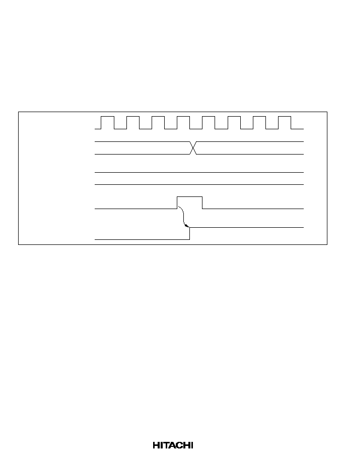
203
9.3.2
Compare-Match Timing
Setting of Compare-Match Flags A and B (CMFA and CMFB): The compare-match flags are
set to 1 by an internal compare-match signal generated when the timer count matches the time
constant in TCORA or TCORB. The compare-match signal is generated at the last state in which
the match is true, just before the timer counter increments to a new value.
Accordingly, when the timer count matches one of the time constants, the compare-match signal is
not generated until the next period of the clock source. Figure 9.4 shows the timing of the setting
of the compare-match flags.
TCOR
¯
Internal compare-
match signal
TCNT
N
N
N + 1
CMF
Figure 9.4 Setting of Compare-Match Flags
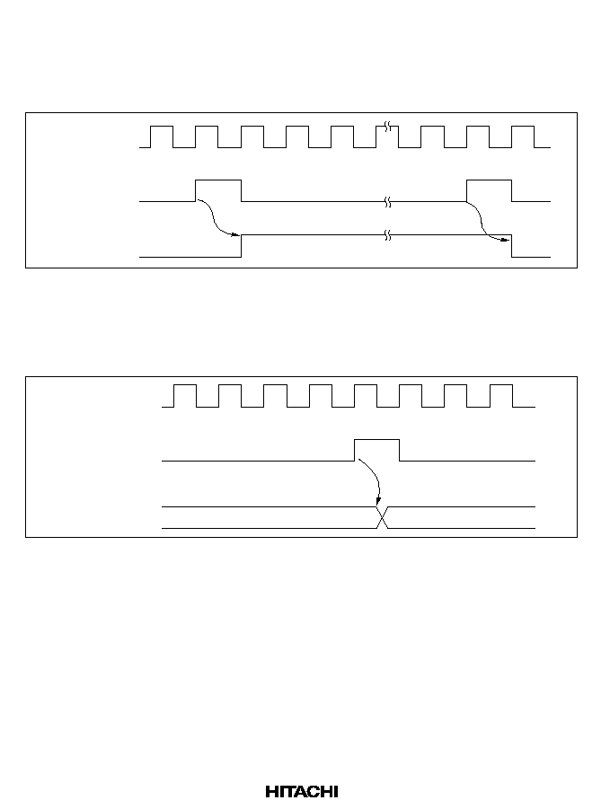
204
Output Timing: When a compare-match event occurs, the timer output changes as specified by
the output select bits (OS3 to OS0) in the TCSR. Depending on these bits, the output can remain
the same, change to 0, change to 1, or toggle.
Figure 9.5 shows the timing when the output is set to toggle on compare-match A.
Timer output
(TMO)
¯
Internal compare-
match A signal
Figure 9.5 Timing of Timer Output
Timing of Compare-Match Clear: Depending on the CCLR1 and CCLR0 bits in TCR, the timer
counter can be cleared when compare-match A or B occurs. Figure 9.6 shows the timing of this
operation.
TCNT
¯
Internal compare-
match signal
N
H'00
Figure 9.6 Timing of Compare-Match Clear
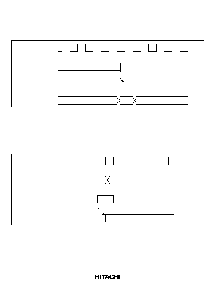
205
9.3.3
External Reset of TCNT
When the CCLR1 and CCLR0 bits in TCR are both set to 1, the timer counter is cleared on the
rising edge of an external reset input. Figure 9.7 shows the timing of this operation. The timer
reset pulse width must be at least 1.5 system clock (¯) periods.
Internal clear
pulse
¯
TCNT
External reset
input (TMRI)
N ≠ 1
N
H'00
Figure 9.7 Timing of External Reset
9.3.4
Setting of Overflow Flag (OVF)
The overflow flag (OVF) in TCSR is set to 1 when the timer count overflows (changes from H'FF
to H'00). Figure 9.8 shows the timing of this operation.
H'FF
H'00
Internal overflow
signal
¯
TCNT
OVF
Figure 9.8 Setting of Overflow Flag (OVF)
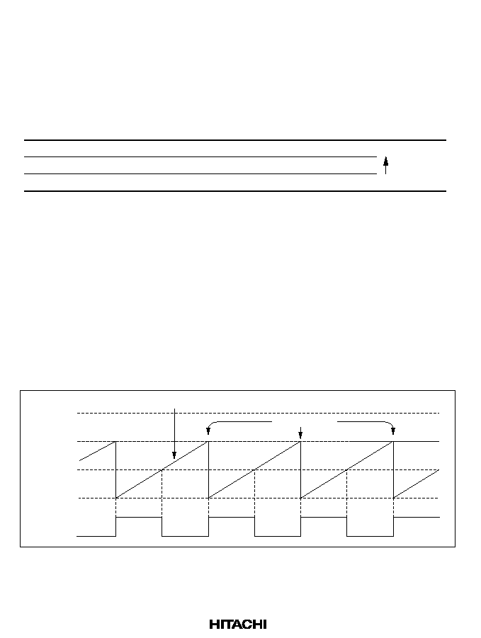
206
9.4
Interrupts
Each channel in the 8-bit timer can generate three types of interrupts: compare-match A and B
(CMIA and CMIB), and overflow (OVI). Each interrupt can be enabled or disabled by an enable
bit in TCR. Independent signals are sent to the interrupt controller for each interrupt. Table 9.3
lists information about these interrupts.
Table 9.3
8-Bit Timer Interrupts
Interrupt
Description
Priority
CMIA
Requested by CMFA
High
CMIB
Requested by CMFB
OVI
Requested by OVF
Low
9.5
Sample Application
In the example below, the 8-bit timer is used to generate a pulse output with a selected duty cycle.
The control bits are set as follows:
1.In TCR, CCLR1 is cleared to 0 and CCLR0 is set to 1 so that the timer counter is cleared when
its value matches the constant in TCORA.
2.In TCSR, bits OS3 to OS0 are set to 0110, causing the output to change to 1 on compare-match
A and to 0 on compare-match B.
With these settings, the 8-bit timer provides output of pulses at a rate determined by TCORA with
a pulse width determined by TCORB. No software intervention is required.
TCNT
Clear counter
H'FF
TCORA
TCORB
H'00
TMO
Figure 9.9 Example of Pulse Output

207
9.6
Application Notes
Application programmers should note that the following types of contention can occur in the 8-bit
timer.
9.6.1
Contention between TCNT Write and Clear
If an internal counter clear signal is generated during the T
3
state of a write cycle to the timer
counter, the clear signal takes priority and the write is not performed.
Figure 9.10 shows this type of contention.
T
1
T
2
T
3
Write cycle: CPU writes to TCNT
Internal address
bus
TCNT address
Internal write
signal
¯
Counter clear
signal
TCNT
N
H'00
Figure 9.10 TCNT Write-Clear Contention

208
9.6.2
Contention between TCNT Write and Increment
If a timer counter increment pulse is generated during the T
3
state of a write cycle to the timer
counter, the write takes priority and the timer counter is not incremented.
Figure 9.11 shows this type of contention.
T
1
T
2
T
3
Write cycle: CPU writes to TCNT
Internal address bus
Internal write signal
¯
TCNT clock pulse
TNCT
N
M
Write data
TCNT address
Figure 9.11 TCNT Write-Increment Contention
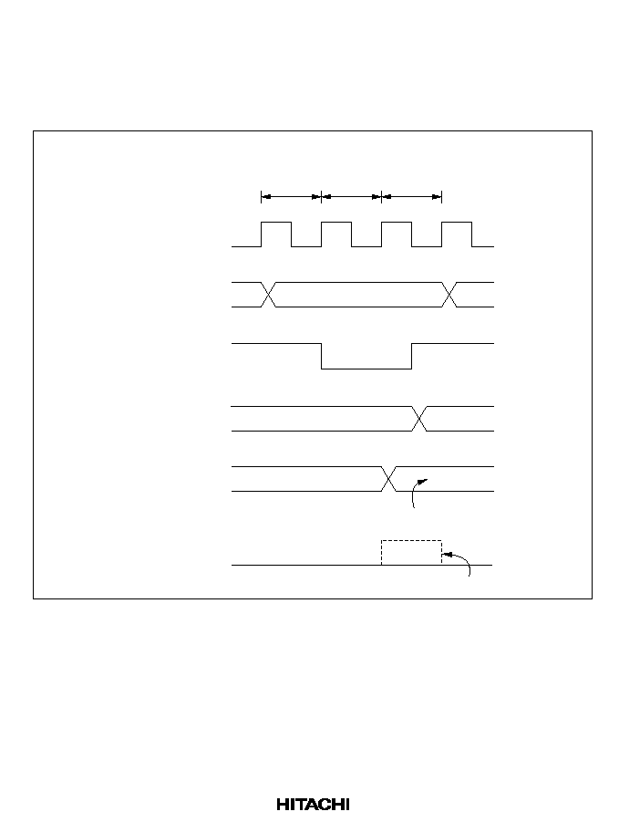
209
9.6.3
Contention between TCOR Write and Compare-Match
If a compare-match occurs during the T
3
state of a write cycle to TCOR, the write takes priority
and the compare-match signal is inhibited.
Figure 9.12 shows this type of contention.
T
1
T
2
T
3
Write cycle: CPU writes to TCOR
Internal address bus
Internal write signal
¯
TCNT
TCOR
N
M
TCOR write data
TCOR address
N
N + 1
Compare-match
A or B signal
Inhibited
Figure 9.12 Contention between TCOR Write and Compare-Match

210
9.6.4
Contention between Compare-Match A and Compare-Match B
If identical time constants are written in TCORA and TCORB, causing compare-match A and B to
occur simultaneously, any conflict between the output selections for compare-match A and B is
resolved by following the priority order in table 9.4.
Table 9.4
Priority of Timer Output
Output Selection
Priority
Toggle
High
1 output
0 output
No change
Low
9.6.5
Increment Caused by Changing of Internal Clock Source
When an internal clock source is changed, the changeover may cause the timer counter to
increment. This depends on the time at which the clock select bits (CKS1, CKS0) are rewritten, as
shown in table 9.5.
The pulse that increments the timer counter is generated at the falling edge of the internal clock
source signal. If clock sources are changed when the old source is high and the new source is low,
as in case no. 3 in table 9.5, the changeover generates a falling edge that triggers the TCNT clock
pulse and increments the timer counter.
Switching between an internal and external clock source can also cause the timer counter to
increment.
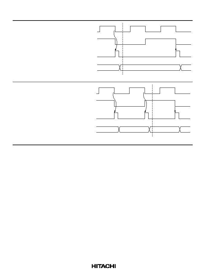
211
Table 9.5
Effect of Changing Internal Clock Sources
No.
Description
Timing
1
Low
low
*
1
N + 1
Old clock
source
New clock
source
TCNT clock
pulse
TCNT
CKS rewrite
N
2
Low
high
*
2
N + 1
N + 2
Old clock
source
New clock
source
TCNT clock
pulse
TCNT
CKS rewrite
N

212
No.
Description
Timing
3
High
low
*
3
N + 1
N
N + 2
*
4
Old clock
source
New clock
source
TCNT clock
pulse
TCNT
CKS rewrite
4High
high
N + 1
N + 2
N
Old clock
source
New clock
source
TCNT clock
pulse
CKS rewrite
TCNT
Notes:
*
1 Including a transition from low to the stopped state (CKS1 = 0, CKS0 = 0), or a
transition from the stopped state to low.
*
2 Including a transition from the stopped state to high.
*
3 Including a transition from high to the stopped state.
*
4The switching of clock sources is regarded as a falling edge that increments TCNT.

213
Section 10 PWM Timers
10.1
Overview
The H8/3337 Series and H8/3397 Series have an on-chip pulse-width modulation (PWM) timer
module with two independent channels (PWM0 and PWM1). Both channels are functionally
identical. Each PWM channel generates a rectangular output pulse with a duty cycle of 0 to 100%.
The duty cycle is specified in an 8-bit duty register (DTR).
10.1.1
Features
The PWM timer module has the following features:
∑
Selection of eight clock sources
∑
Duty cycles from 0 to 100% with 1/250 resolution
∑
Direct or inverted PWM output, and software enable/disable control

214
10.1.2
Block Diagram
Figure 10.1 shows a block diagram of one PWM timer channel.
Comparator
DTR
Bus interface
Internal
data bus
Pulse
TCR
TCNT
Compare-match
¯
P
/2
¯
P
/8
¯
P
/32
¯
P
/128
¯
P
/256
¯
P
/1024
¯
P
/2048
¯
P
/4096
Output
control
Clock
Clock
select
Internal clock sources
DTR:
TCNT:
TCR:
Duty register (8 bits)
Timer counter (8 bits)
Timer control register (8 bits)
Module data bus
Figure 10.1 Block Diagram of PWM Timer (One Channel)
10.1.3
Input and Output Pins
Table 10.1 lists the output pins of the PWM timer module. There are no input pins.
Table 10.1
Output Pins of PWM Timer Module
Name
Abbreviation
I/O
Function
PWM0 output
PW
0
Output
Pulse output from PWM timer channel 0.
PWM1 output
PW
1
Output
Pulse output from PWM timer channel 1.
215
10.1.4
Register Configuration
The PWM timer module has three registers for each channel as listed in table 10.2.
Table 10.2
PWM Timer Registers
Initial
Address
Name
Abbreviation
R/W
Value
PWM0
PWM1
Timer control register
TCR
R/W
H'38
H'FFA0
H'FFA4
Duty register
DTR
R/W
H'FF
H'FFA1
H'FFA5
Timer counter
TCNT
R/W
H'00
H'FFA2
H'FFA6
10.2
Register Descriptions
10.2.1
Timer Counter (TCNT)
Bit
7
6
5
4
3
2
1
0
Initial value
0
0
0
0
0
0
0
0
Read/Write
R/W
R/W
R/W
R/W
R/W
R/W
R/W
R/W
TCNT is an 8-bit readable/writable up-counter. When the output enable bit (OE) is set to 1 in
TCR, TCNT starts counting pulses of an internal clock source selected by clock select bits 2 to 0
(CKS2 to CKS0). After counting from H'00 to H'F9, the count repeats from H'00. When TCNT
changes from H'00 to to H'01, the PWM output is placed in the 1 state, unless the DTR value is
H'00, in which case the duty cycle is 0% and the PWM output remains in the 0 state.
TCNT is initialized to H'00 at a reset and in the standby modes, and when the OE bit is cleared to
0.

216
10.2.2
Duty Register (DTR)
Bit
7
6
5
4
3
2
1
0
Initial value
1
1
1
1
1
1
1
1
Read/Write
R/W
R/W
R/W
R/W
R/W
R/W
R/W
R/W
DTR is an 8-bit readable/writable register that specifies the duty cycle of the output pulse. Any
duty cycle from 0% to 100% can be output by setting the corresponding value in DTR. The
resolution is 1/250. Writing 0 (H'00) in DTR gives a 0% duty cycle. Writing 125 (H'7D) gives a
50% duty cycle. Writing 250 (H'FA) gives a 100% duty cycle.
The DTR and TCNT values are always compared. When the values match, the PWM output is
placed in the 0 state.
DTR is double-buffered. A new value written in DTR does not become valid until after the timer
count changes from H'F9 to H'00. While the OE bit is cleared to 0 in TCR, however, new values
written in DTR become valid immediately. When DTR is read, the value read is the currently valid
value.
DTR is initialized to H'FF by a reset and in the standby modes.
217
10.2.3
Timer Control Register (TCR)
Bit
7
6
5
4
3
2
1
0
OE
OS
--
--
--
CKS2
CKS1
CKS0
Initial value
0
0
1
1
1
0
0
0
Read/Write
R/W
R/W
--
--
--
R/W
R/W
R/W
TCR is an 8-bit readable/writable register that selects the clock input to TCNT and controls PWM
output.
TCR is initialized to H'38 by a reset and in standby mode.
Bit 7--Output Enable (OE): This bit enables the timer counter and the PWM output.
Bit 7: OE
Description
0
PWM output is disabled. TCNT is cleared to H'00 and stopped.
(Initial value)
1
PWM output is enabled. TCNT runs.
Bit 6--Output Select (OS): This bit selects positive or negative logic for the PWM output.
Bit 6: OS
Description
0
Positive logic; positive-going PWM pulse, 1 = high
(Initial value)
1
Negative logic; negative-going PWM pulse, 1 = low
Bits 5 to 3--Reserved: These bits cannot be modified and are always read as 1.

218
Bits 2, 1, and 0--Clock Select (CKS2, CKS1, and CKS0): These bits select one of eight internal
clock sources obtained by dividing the supporting-module clock (¯
P
).
Bit 2: CKS2
Bit 1: CKS1
Bit 0: CKS0
Description
0
0
0
¯
P
/2
(Initial value)
1
¯
P
/8
1
0
¯
P
/32
1
¯
P
/128
1
0
0
¯
P
/256
1
¯
P
/1024
1
0
¯
P
/2048
1
¯
P
/4096
From the clock source frequency, the resolution, period, and frequency of the PWM output can be
calculated as follows.
Resolution = 1/clock source frequency
PWM period = resolution
◊
250
PWM frequency = 1/PWM period
If the ¯
P
clock frequency is 10 MHz, then the resolution, period, and frequency of the PWM output
for each clock source are as shown in table 10.3.
Table 10.3
PWM Timer Parameters for 10 MHz System Clock
Internal Clock Frequency
Resolution
PWM Period
PWM Frequency
¯
P
/2
200 ns
50 µs
20 kHz
¯
P
/8
800 ns
200 µs
5 kHz
¯
P
/32
3.2 µs
800 µs
1.25 kHz
¯
P
/128
12.8 µs
3.2 ms
312.5 Hz
¯
P
/256
25.6 µs
6.4 ms
156.3 Hz
¯
P
/1024
102.4 µs
25.6 ms
39.1 Hz
¯
P
/2048
204.8 µs
51.2 ms
19.5 Hz
¯
P
/4096
409.6 µs
102.4 ms
9.8 Hz
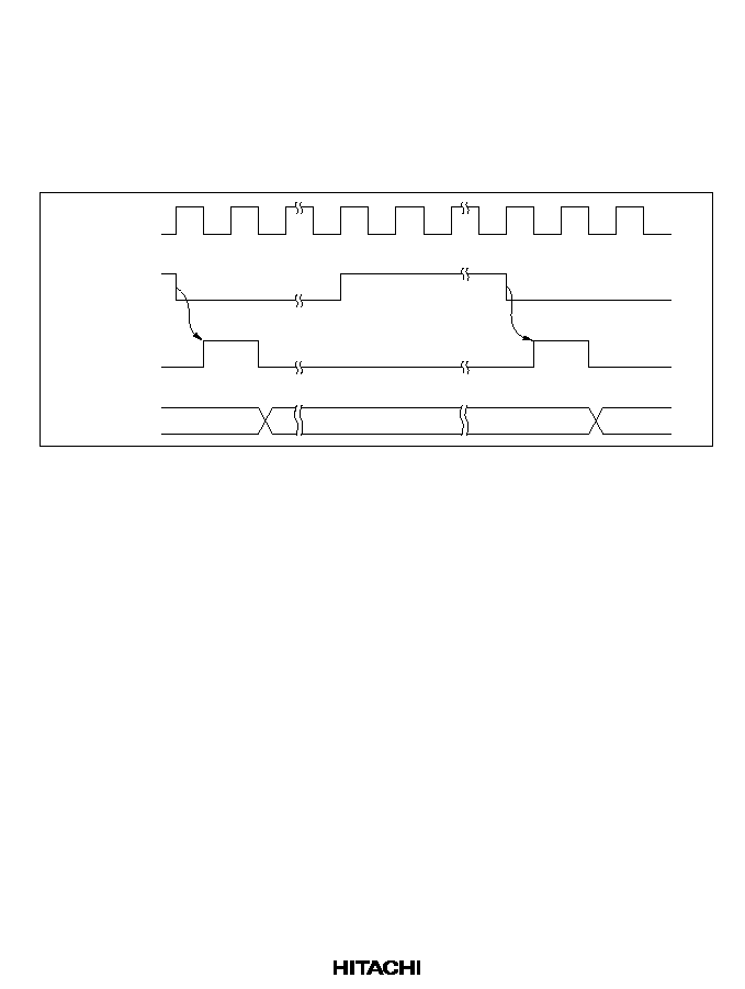
219
10.3
Operation
10.3.1
Timer Incrementation
The PWM clock source is created by dividing the system clock (¯). The timer counter increments
on a TCNT clock pulse generated from the falling edge of the prescaler output as shown in figure
10.2.
N ≠ 1
TCNT clock
pulse
¯
TCNT
Prescaler
output
N
N + 1
Figure 10.2 TCNT Increment Timing
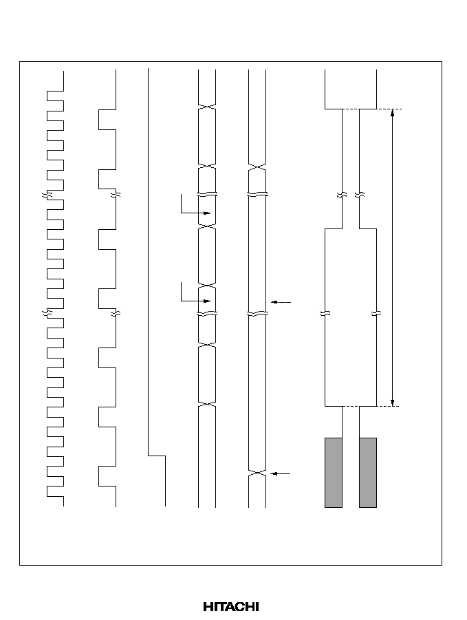
220
10.3.2
PWM Operation
Figure 10.3 is a timing chart of the PWM operation.
N ≠ 1
N + 1
(a) H'00
(b) H'01
H'02
N
H'F9
(d) H'00
H'01
N
(d) M
H'FF
(c)
(a)
*
(e)
*
(b)
(c)
N written in DTR
M written in DTR
¯
TCNT clock
pulses
OE
TCNT
DTR
(OS = 0)
PWM output
(OS = 1)
One PWM cycle
Note:
*
State depends on values in data register and data direction register.
Figure 10.3 PWM Timing

221
Direct Output (OS = 0)
1. When (OE = 0)--(a) in Figure 10.3
The timer count is held at H'00 and PWM output is inhibited. [Pin 4
6
(for PW0) or pin 4
7
(for
PW1) is used for port 4 input/output, and its state depends on the corresponding port 4 data
register and data direction register.] Any value (such as N in figure 10.3) written in the DTR
becomes valid immediately.
2. When (OE = 1)
a. The timer counter begins incrementing. The PWM output goes high when TCNT changes
from H'00 to H'01, unless DTR = H'00. [(b) in figure 10.3]
b. When the count passes the DTR value, the PWM output goes low. [(c) in figure 10.3]
c. If the DTR value is changed (by writing the data "M" in figure 10.3), the new value
becomes valid after the timer count changes from H'F9 to H'00. [(d) in figure 10.3]
Inverted Output (OS = 1)--(e) in Figure 10.3: The operation is the same except that high and
low are reversed in the PWM output. [(e) in figure 10.3]
10.4
Application Notes
Some notes on the use of the PWM timer module are given below.
1. Any necessary changes to the clock select bits (CKS2 to CKS0) and output select bit (OS)
should be made before the output enable bit (OE) is set to 1.
2. If the DTR value is H'00, the duty cycle is 0% and PWM output remains constant at 0.
If the DTR value is H'FA to H'FF, the duty cycle is 100% and PWM output remains constant at
1.
(For direct output, 0 is low and 1 is high. For inverted output, 0 is high and 1 is low.)

222

223
Section 11 Watchdog Timer
11.1
Overview
The H8/3337 Series and H8/3397 Series have an on-chip watchdog timer (WDT) that can monitor
system operation by resetting the CPU or generating a nonmaskable interrupt if a system crash
allows the timer count to overflow.
When this watchdog function is not needed, the watchdog timer module can be used as an interval
timer. In interval timer mode, it requests an WOVF interrupt at each counter overflow.
11.1.1
Features
WDT features are shown below.
∑
Selection of eight counter input clocks
∑
Switchable between watchdog timer mode and interval timer mode
∑
Timer counter overflow generates an internal reset or internal interrupt:
Selection of internal reset or internal interrupt generation in watchdog timer mode
WOVF interrupt request in interval timer mode

224
11.1.2
Block Diagram
Figure 11.1 is a block diagram of the watchdog timer.
Interrupt
control
Internal reset or
internal NMI
(Watchdog timer mode)
WOVF interrupt
request signal
(Interval timer mode)
Overflow
TCNT
TCSR
Read/write
control
Internal
data bus
Clock
select
¯
P
/2
¯
P
/32
¯
P
/64
¯
P
/128
¯
P
/256
¯
P
/512
¯
P
/2048
¯
P
/4096
Internal clock source
Clock
TCNT:
TCSR:
Timer counter
Timer control/status register
Figure 11.1 Block Diagram of Watchdog Timer
11.1.3
Register Configuration
Table 11.1 lists information on the watchdog timer registers.
Table 11.1
Register Configuration
Initial
Addresses
Name
Abbreviation
R/W
Value
Write
Read
Timer control/status register
TCSR
R/(W)
*
H'10
H'FFA8
H'FFA8
Timer counter
TCNT
R/W
H'00
H'FFA8
H'FFA9
Note:
*
Software can write a 0 to clear the status flag bits, but cannot write 1.

225
11.2
Register Descriptions
11.2.1
Timer Counter (TCNT)
Bit
7
6
5
4
3
2
1
0
Initial value
0
0
0
0
0
0
0
0
Read/Write
R/W
R/W
R/W
R/W
R/W
R/W
R/W
R/W
TCNT is an 8-bit readable/writable up-counter. When the timer enable bit (TME) in the timer
control/status register (TCSR) is set to 1, the timer counter starts counting pulses of an internal
clock source selected by clock select bits 2 to 0 (CKS2 to CKS0) in TCSR. When the count
overflows (changes from H'FF to H'00), an overflow flag (OVF) in TCSR is set to 1.
TCNT is initialized to H'00 by a reset and when the TME bit is cleared to 0.
Note:
TCNT is write-protected by a password. See Section 11.2.3, Register Access, for details.
11.2.2
Timer Control/Status Register (TCSR)
Bit
7
6
5
4
3
2
1
0
OVF
WT/
IT
TME
--
RST/
NMI
CKS2
CKS1
CKS0
Initial value
0
0
0
1
0
0
0
0
Read/Write
R/(W)
*
R/W
R/W
--
R/W
R/W
R/W
R/W
Note:
*
Software can write a 0 in bit 7 to clear the flag, but cannot write a 1 in this bit.
TCSR is an 8-bit readable/writable register that selects the timer mode and clock source and
performs other functions.
Bits 7 to 5 and bit 3 are initialized to 0 by a reset and in the standby modes. Bits 2 to 0 are
initialized to 0 by a reset, but retain their values in the standby modes.
Note:
TCSR is write-protected by a password. See section 11.2.3, Register Access, for details.

226
Bit 7--Overflow Flag (OVF): Indicates that the watchdog timer count has overflowed from H'FF
to H'00.
Bit 7: OVF
Description
0
To clear OVF, the CPU must read OVF after it has been set to 1, then write a 0
in this bit
(Initial value)
1
Set to 1 when TCNT changes from H'FF to H'00
Bit 6--Timer Mode Select (WT/
IT): Selects whether to operate in watchdog timer mode or
interval timer mode. When TCNT overflows, an WOVF interrupt request is sent to the CPU in
interval timer mode. For watchdog timer mode, a reset or NMI interrupt is requested.
Bit 6: WT/
IT
Description
0
Interval timer mode (WOVF request)
(Initial value)
1
Watchdog timer mode (reset or NMI request)
Bit 5--Timer Enable (TME): Enables or disables the timer.
Bit 5: TME
Description
0
TCNT is initialized to H'00 and stopped
(Initial value)
1
TCNT runs and requests a reset or an interrupt when it overflows
Bit 4--Reserved: This bit cannot be modified and is always read as 1.
Bit 3: Reset or NMI Select (RST/
NMI): Selects either an internal reset or internal NMI function
at watchdog timer overflow.
Bit 3: RST/
NMI
Description
0
NMI function enabled
(Initial value)
1
Reset function enabled

227
Bits 2to 0-- Clock Select (CKS2≠CKS0): These bits select one of eight clock sources obtained
by dividing the system clock (¯).
The overflow interval is the time from when the watchdog timer counter begins counting from
H'00 until an overflow occurs. In interval timer mode, WOVF interrupts are requested at this
interval.
Bit 2:
CKS2
Bit 1:
CKS1
Bit 0:
CKS0
Description
Overflow Interval (¯
P
= 10 MHz)
0
0
0
¯
P
/2
51.2 µs
(Initial value)
1
¯
P
/32
819.2 µs
1
0
¯
P
/64
1.6 ms
1
¯
P
/128
3.3 ms
1
0
0
¯
P
/256
6.6 ms
1
¯
P
/512
13.1 ms
1
0
¯
P
/2048
52.4 ms
1
¯
P
/4096
104.9 ms
11.2.3
System Control Register (SYSCR)
Bit
7
6
5
4
3
2
1
0
SSBY
STS2
STS1
STS0
XRST
NMIEG
HIE
RAME
Initial value
0
0
0
0
1
0
0
1
Read/Write
R/W
R/W
R/W
R/W
R
R/W
R/W
R/W
Only bit 3 is described here. For details of other bits, see section 3.2., System Control Register
(SYSCR), and descriptions of the relevant modules.
Bit 3--External Reset (XRST): Indicates the reset source. When the watchdog timer is used, a
reset can be generated by watchdog timer overflow as well as by external reset input.
XRST is a read-only bit. It is set to 1 by an external reset and cleared to 0 by an internal reset due
to watchdog timer overflow when the RST/
NMI bit is 1.
Bit 3: XRSTDescription
0
A reset is generated by an internal reset due to watchdog timer overflow
1
A reset is generated by external reset input
(Initial value)

228
11.2.4
Register Access
The watchdog timer's TCNT and TCSR registers are more difficult to write to than other registers.
The procedures for writing and reading these registers are given below.
Writing to TCNT and TCSR: Word access is required. Byte data transfer instructions cannot be
used for write access.
The TCNT and TCSR registers have the same write address. The write data must be contained in
the lower byte of a word written at this address. The upper byte must contain H'5A (password for
TCNT) or H'A5 (password for TCSR). See figure 11.2. The result of the access depicted in figure
11.2 is to transfer the write data from the lower byte to TCNT or TCSR.
Write data
H'5A
15
8 7
0
Write data
H'A5
15
8 7
0
H'FFA8
H'FFA8
Writing to TCNT
Writing to TCSR
Address
Address
Figure 11.2 Writing to TCNT and TCSR
Reading TCNT and TCSR: The read addresses are H'FFA8 for TCSR and H'FFA9 for TCNT, as
indicated in table 11.2.
These two registers are read like other registers. Byte access instructions can be used.
Table 11.2
Read Addresses of TCNT and TCSR
Read Address
Register
H'FFA8
TCSR
H'FFA9
TCNT
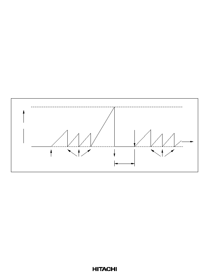
229
11.3
Operation
11.3.1
Watchdog Timer Mode
The watchdog timer function begins operating when software sets the WT/
IT and TME bits to 1 in
TCSR. Thereafter, software should periodically rewrite the contents of the timer counter (normally
by writing H'00) to prevent the count from overflowing. If a program crash allows the timer count
to overflow, the entire chip is reset for 518 system clocks (518 ¯), or an NMI interrupt is
requested. Figure 11.3 shows the operation.
NMI requests from the watchdog timer have the same vector as NMI requests from the
NMI pin.
Avoid simultaneous handling of watchdog timer NMI requests and NMI requests from pin
NMI.
A reset from the watchdog timer has the same vector as an external reset from the
RES pin. The
reset source can be determined by the XRST bit in SYSCR.
H'FF
H'00
TCNT count
WDT overflow
WT/
IT
= 1
TME = 1
H'00 written
to TCNT
OVF = 1
Reset
518 ¯
H'00 written
to TCNT
WT/
IT
= 1
TME = 1
Time t
Figure 11.3 Operation in Watchdog Timer Mode

230
11.3.2
Interval Timer Mode
Interval timer operation begins when the WT/
IT bit is cleared to 0 and the TME bit is set to 1.
In interval timer mode, an WOVF request is generated each time the timer count overflows. This
function can be used to generate WOVF requests at regular intervals. See figure 11.4.
H'FF
H'00
WT/
IT
= 0
TME = 1
Time t
WOVF
request
WOVF
request
WOVF
request
WOVF
request
WOVF
request
TCNT count
Figure 11.4 Operation in Interval Timer Mode
11.3.3
Setting the Overflow Flag
The OVF bit is set to 1 when the timer count overflows. Simultaneously, the WDT module
requests an internal reset, NMI, or WOVF interrupt. The timing is shown in figure 11.5.
H'FF
H'00
¯
TCNT
Internal overflow
signal
OVF
Figure 11.5 Setting the OVF Bit

231
11.4
Application Notes
11.4.1
Contention between TCNT Write and Increment
If a timer counter clock pulse is generated during the T
3
state of a write cycle to the timer counter,
the write takes priority and the timer counter is not incremented. See figure 11.6.
TCNT address
N
M
Counter write data
Internal address bus
Internal write signal
TCNT clock pulse
TCNT
¯
T
3
T
2
T
1
Write cycle (CPU writes to TCNT)
Figure 11.6 TCNT Write-Increment Contention
11.4.2
Changing the Clock Select Bits (CKS2 to CKS0)
Software should stop the watchdog timer (by clearing the TME bit to 0) before changing the value
of the clock select bits. If the clock select bits are modified while the watchdog timer is running,
the timer count may be incremented incorrectly.
11.4.3
Recovery from Software Standby Mode
TCSR bits, except bits 0≠2, and the TCNT counter are reset when the chip recovers from software
standby mode. Re-initialize the watchdog timer as necessary to resume normal operation.

232
11.4.4
Switching between Watchdog Timer Mode and Interval Timer Mode
If a switch is made between watchdog timer mode and interval timer mode while the WDT is
operating, correct operation may not be performed. The WDT must be stopped (by clearing the
TME bit to 0) before changing the timer mode.
11.4.5
Detection of Program Runaway
The following points should be noted when using the microcomputer's on-chip watchdog timer to
detect program runaway.
During program runaway, instructions other than the usual instructions may be executed. If an
instruction reserved for system use is executed as a result of runaway, the watchdog timer may
sometimes stop, preventing detection of the runaway.
This problem can be avoided by making the following settings in the program.
1. Set code H'0004 in ROM address H'0002.
2. Set code H'56F0 in ROM address H'0004.
As system reserved addresses may be used by an emulator, the above settings should only be made
for the real chip.

233
Section 12 Serial Communication Interface
12.1
Overview
The H8/3337 Series and H8/3397 Series include two serial communication interface channels
(SCI0 and SCI1) for transferring serial data to and from other chips. Either synchronous or
asynchronous communication can be selected.
12.1.1
Features
The features of the on-chip serial communication interface are:
∑
Asynchronous mode
The H8/3337 Series and H8/3397 Series can communicate with a UART (Universal
Asynchronous Receiver/Transmitter), ACIA (Asynchronous Communication Interface
Adapter), or other chip that employs standard asynchronous serial communication. It also has a
multiprocessor communication function for communication with other processors. Twelve data
formats are available.
Data length: 7 or 8 bits
Stop bit length: 1 or 2 bits
Parity: Even, odd, or none
Multiprocessor bit: 1 or 0
Error detection: Parity, overrun, and framing errors
Break detection: When a framing error occurs, the break condition can be detected by
reading the level of the RxD line directly.
∑
Synchronous mode
The SCI can communicate with chips able to perform clocked synchronous data transfer.
Data length: 8 bits
Error detection: Overrun errors
∑
Full duplex communication
The transmitting and receiving sections are independent, so each channel can transmit and
receive simultaneously. Both the transmit and receive sections use double buffering, so
continuous data transfer is possible in either direction.
∑
Built-in baud rate generator
Any specified bit rate can be generated.
∑
Internal or external clock source
The SCI can operate on an internal clock signal from the baud rate generator, or an external
clock signal input at the SCK0 or SCK1 pin.
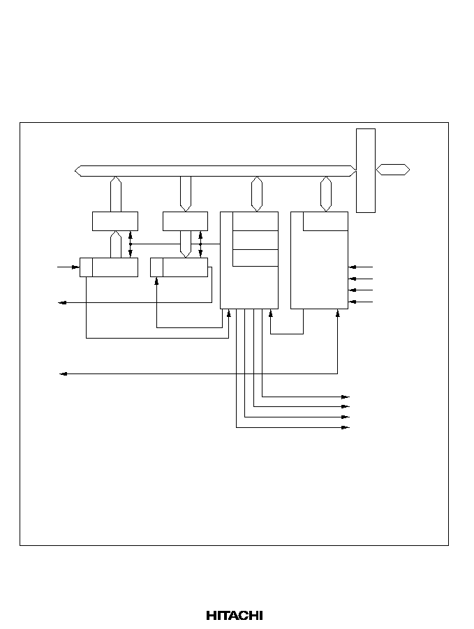
234
∑
Four interrupts
TDR-empty, TSR-empty, receive-end, and receive-error interrupts are requested
independently.
12.1.2
Block Diagram
Figure 12.1 shows a block diagram of one serial communication interface channel.
TDR
Bus interface
Internal
data bus
Parity
generate
Clock
Parity check
TSR
¯
¯
P
/4
¯
P
/16
¯
P
/64
RxD
TxD
TXI
RXI
ERI
Interrupt signals
External clock source
Internal
clock
RDR
RSR
SCK
BRR
Communi-
cation
control
SSR
SCR
SMR
Baud rate
generator
RSR:
RDR:
TSR:
TDR:
SMR:
SCR:
SSR:
BRR:
Receive shift register (8 bits)
Receive data register (8 bits)
Transmit shift register (8 bits)
Transmit data register (8 bits)
Serial mode register (8 bits)
Serial control register (8 bits)
Serial status register (8 bits)
Bit rate register (8 bits)
TEI
Module data bus
Figure 12.1 Block Diagram of Serial Communication Interface

235
12.1.3
Input and Output Pins
Table 12.1 lists the input and output pins used by the SCI module.
Table 12.1
SCI Input/Output Pins
Channel
Name
Abbreviation
I/O
Function
0
Serial clock input/output
SCK0
Input/output
SCI0 clock input and output
Receive data input
RxD0
Input
SCI0 receive data input
Transmit data output
TxD0
Output
SCI0 transmit data output
1
Serial clock input/output
SCK1
Input/output
SCI1 clock input and output
Receive data input
RxD1
Input
SCI1 receive data input
Transmit data output
TxD1
Output
SCI1 transmit data output
Note:
In this manual, the channel subscript has been deleted, and only SCK, RxD, and TxD are
used.

236
12.1.4
Register Configuration
Table 12.2 lists the SCI registers. These registers specify the operating mode (synchronous or
asynchronous), data format and bit rate, and control the transmit and receive sections.
Table 12.2
SCI Registers
Channel
Name
Abbreviation
R/W
Initial
Value
Address
0
Receive shift register
RSR
--
--
--
Receive data register
RDR
R
H'00
H'FFDD
Transmit shift register
TSR
--
--
--
Transmit data register
TDR
R/W
H'FF
H'FFDB
Serial mode register
SMR
*
2
R/W
H'00
H'FFD8
Serial control register
SCR
R/W
H'00
H'FFDA
Serial status register
SSR
R/(W)
*
1
H'84
H'FFDC
Bit rate register
BRR
*
2
R/W
H'FF
H'FFD9
1
Receive shift register
RSR
--
--
--
Receive data register
RDR
R
H'00
H'FF8D
Transmit shift register
TSR
--
--
--
Transmit data register
TDR
R/W
H'FF
H'FF8B
Serial mode register
SMR
R/W
H'00
H'FF88
Serial control register
SCR
R/W
H'00
H'FF8A
Serial status register
SSR
R/(W)
*
1
H'84
H'FF8C
Bit rate register
BRR
R/W
H'FF
H'FF89
0 and 1
Serial/timer control register
STCR
R/W
H'00
H'FFC3
Notes:
*
1 Software can write a 0 to clear the flags in bits 7 to 3, but cannot write 1 in these bits.
*
2 SMR and BRR have the same addresses as I
2
C bus interface registers ICCR and
ICSR. For the access switching method and other details, see section 13, I
2
C Bus
Interface.

237
12.2
Register Descriptions
12.2.1
Receive Shift Register (RSR)
Bit
7
6
5
4
3
2
1
0
Read/Write
--
--
--
--
--
--
--
--
RSR is a shift register that converts incoming serial data to parallel data. When one data character
has been received, it is transferred to the receive data register (RDR).
The CPU cannot read or write RSR directly.
12.2.2
Receive Data Register (RDR)
Bit
7
6
5
4
3
2
1
0
Initial value
0
0
0
0
0
0
0
0
Read/Write
R
R
R
R
R
R
R
R
RDR stores received data. As each character is received, it is transferred from RSR to RDR,
enabling RSR to receive the next character. This double-buffering allows the SCI to receive data
continuously.
RDR is a read-only register. RDR is initialized to H'00 by a reset and in the standby modes.
12.2.3
Transmit Shift Register (TSR)
Bit
7
6
5
4
3
2
1
0
Read/Write
--
--
--
--
--
--
--
--
TSR is a shift register that converts parallel data to serial transmit data. When transmission of one
character is completed, the next character is moved from the transmit data register (TDR) to TSR
and transmission of that character begins. If the TDRE bit is still set to 1, however, nothing is
transferred to TSR.
The CPU cannot read or write TSR directly.

238
12.2.4
Transmit Data Register (TDR)
Bit
7
6
5
4
3
2
1
0
Initial value
1
1
1
1
1
1
1
1
Read/Write
R/W
R/W
R/W
R/W
R/W
R/W
R/W
R/W
TDR is an 8-bit readable/writable register that holds the next data to be transmitted. When TSR
becomes empty, the data written in TDR is transferred to TSR. Continuous data transmission is
possible by writing the next data in TDR while the current data is being transmitted from TSR.
TDR is initialized to H'FF by a reset and in the standby modes.
12.2.5
Serial Mode Register (SMR)
Bit
7
6
5
4
3
2
1
0
C/
A
CHR
PE
O/
E
STOP
MP
CKS1
CKS0
Initial value
0
0
0
0
0
0
0
0
Read/Write
R/W
R/W
R/W
R/W
R/W
R/W
R/W
R/W
SMR is an 8-bit readable/writable register that controls the communication format and selects the
clock source of the on-chip baud rate generator. It is initialized to H'00 by a reset and in the
standby modes. For further information on the SMR settings and communication formats, see
tables 12.5 and 12.7 in section 12.3, Operation.
Bit 7--Communication Mode (C/
A): This bit selects asynchronous or synchronous
communication mode.
Bit 7: C/
A
Description
0
Asynchronous communication
(Initial value)
1
Synchronous communication
Bit 6--Character Length (CHR): This bit selects the character length in asynchronous mode.
It is ignored in synchronous mode.
Bit 6: CHR
Description
0
8 bits per character
(Initial value)
1
7 bits per character (Bits 0 to 6 of TDR and RDR are used for transmitting and
receiving, respectively.)

239
Bit 5--Parity Enable (PE): This bit selects whether to add a parity bit in asynchronous mode.
It is ignored in synchronous mode, and when a multiprocessor format is used.
Bit 5: PE
Description
0
Transmit: No parity bit is added.
(Initial value)
Receive: Parity is not checked.
1
Transmit: A parity bit is added.
Receive: Parity is checked.
Bit 4--Parity Mode (O/
E): In asynchronous mode, when parity is enabled (PE = 1), this bit
selects even or odd parity.
Even parity means that a parity bit is added to the data bits for each character to make the total
number of 1's even. Odd parity means that the total number of 1's is made odd.
This bit is ignored when PE = 0, or when a multiprocessor format is used. It is also ignored in
synchronous mode.
Bit 4: O/
E
Description
0
Even parity
(Initial value)
1
Odd parity
Bit 3--Stop Bit Length (STOP): This bit selects the number of stop bits. It is ignored in
synchronous mode.
Bit 3: STOP
Description
0
One stop bit
(Initial value)
Transmit: One stop bit is added.
Receive: One stop bit is checked to detect framing errors.
1
Two stop bits
Transmit: Two stop bits are added.
Receive: The first stop bit is checked to detect framing errors. If the second
stop bit is a space (0), it is regarded as the next start bit.

240
Bit 2--Multiprocessor Mode (MP): This bit selects the multiprocessor format in asynchronous
communication. When multiprocessor format is selected, the parity settings of the parity enable bit
(PE) and parity mode bit (O/
E) are ignored. The MP bit is ignored in synchronous communication.
The MP bit is valid only when the MPE bit in the serial/timer control register (STCR) is set to 1.
When the MPE bit is cleared to 0, the multiprocessor communication function is disabled
regardless of the setting of the MP bit.
Bit 2: MP
Description
0
Multiprocessor communication function is disabled.
(Initial value)
1
Multiprocessor communication function is enabled.
Bits 1 and 0--Clock Select 1 and 0 (CKS1 and CKS0): These bits select the clock source of the
on-chip baud rate generator.
Bit 1: CKS1
Bit 0: CKS0
Description
0
0
¯ clock
(Initial value)
1
¯
P
/4 clock
1
0
¯
P
/16 clock
1
¯
P
/64 clock
12.2.6
Serial Control Register (SCR)
Bit
7
6
5
4
3
2
1
0
TIE
RIE
TE
RE
MPIE
TEIE
CKE1
CKE0
Initial value
0
0
0
0
0
0
0
0
Read/Write
R/W
R/W
R/W
R/W
R/W
R/W
R/W
R/W
SCR is an 8-bit readable/writable register that enables or disables various SCI functions.
It is initialized to H'00 by a reset and in the standby modes.
Bit 7--Transmit Interrupt Enable (TIE): This bit enables or disables the TDR-empty interrupt
(TXI) requested when the transmit data register empty (TDRE) bit in the serial status register
(SSR) is set to 1.
Bit 7: TIE
Description
0
The TDR-empty interrupt request (TXI) is disabled.
(Initial value)
1
The TDR-empty interrupt request (TXI) is enabled.

241
Bit 6--Receive Interrupt Enable (RIE): This bit enables or disables the receive-end interrupt
(RXI) requested when the receive data register full (RDRF) bit in the serial status register (SSR) is
set to 1, and the receive error interrupt (ERI) requested when the overrun error (ORER), framing
error (FER), or parity error (PER) bit in the serial status register (SSR) is set to 1.
Bit 6: RIE
Description
0
The receive-end interrupt (RXI) and receive-error (ERI) requests are disabled.
(Initial value)
1
The receive-end interrupt (RXI) and receive-error (ERI) requests are enabled.
Bit 5--Transmit Enable (TE): This bit enables or disables the transmit function. When the
transmit function is enabled, the TxD pin is automatically used for output. When the transmit
function is disabled, the TxD pin can be used as a general-purpose I/O port.
Bit 5: TE
Description
0
The transmit function is disabled.
(Initial value)
The TxD pin can be used for general-purpose I/O.
1
The transmit function is enabled. The TxD pin is used for output.
Bit 4--Receive Enable (RE): This bit enables or disables the receive function. When the receive
function is enabled, the RxD pin is automatically used for input. When the receive function is
disabled, the RxD pin is available as a general-purpose I/O port.
Bit 4: RE
Description
0
The receive function is disabled. The RxD pin can be used for general-purpose
I/O.
(Initial value)
1
The receive function is enabled. The RxD pin is used for input.
Bit 3--Multiprocessor Interrupt Enable (MPIE): When serial data is received in a
multiprocessor format, this bit enables or disables the receive-end interrupt (RXI) and receive-
error interrupt (ERI) until data with the multiprocessor bit set to 1 is received. It also enables or
disables the transfer of received data from RSR to RDR, and enables or disables setting of the
RDRF, FER, PER, and ORER bits in the serial status register (SSR).
The MPIE bit is ignored when the MP bit is cleared to 0, and in synchronous mode.
Clearing the MPIE bit to 0 disables the multiprocessor receive interrupt function. In this condition
data is received regardless of the value of the multiprocessor bit in the receive data.

242
Setting the MPIE bit to 1 enables the multiprocessor receive interrupt function. In this condition, if
the multiprocessor bit in the receive data is 0, the receive-end interrupt (RXI) and receive-error
interrupt (ERI) are disabled, the receive data is not transferred from RSR to RDR, and the RDRF,
FER, PER, and ORER bits in the serial status register (SSR) are not set. If the multiprocessor bit is
1, however, the MPB bit in SSR is set to 1, the MPIE bit is cleared to 0, the receive data is
transferred from RSR to RDR, the FER, PER, and ORER bits can be set, and the receive-end and
receive-error interrupts are enabled.
Bit 3: MPIE
Description
0
The multiprocessor receive interrupt function is disabled.
(Initial value)
(Normal receive operation)
1
The multiprocessor receive interrupt function is enabled. During the interval
before data with the multiprocessor bit set to 1 is received, the receive interrupt
request (RXI) and receive-error interrupt request (ERI) are disabled, the RDRF,
FER, PER, and ORER bits are not set in the serial status register (SSR), and
no data is transferred from the RSR to the RDR. The MPIE bit is cleared at the
following times:
1. When 0 is written in MPIE.
2. When data with the multiprocessor bit set to 1 is received.
Bit 2--Transmit-End Interrupt Enable (TEIE): This bit enables or disables the TSR-empty
interrupt (TEI) requested when the transmit-end bit (TEND) in the serial status register (SSR) is
set to 1.
Bit 2: TEIE
Description
0
The TSR-empty interrupt request (TEI) is disabled.
(Initial value)
1
The TSR-empty interrupt request (TEI) is enabled.
Bit 1--Clock Enable 1 (CKE1): This bit selects the internal or external clock source for the baud
rate generator. When the external clock source is selected, the SCK pin is automatically used for
input of the external clock signal.
Bit 1: CKE1
Description
0
Internal clock source
(Initial value)
When C/
A
= 1, the serial clock signal is output at the SCK pin.
When C/
A
= 0, output depends on the CKE0 bit.
1
External clock source. The SCK pin is used for input.

243
Bit 0--Clock Enable 0 (CKE0): When an internal clock source is used in asynchronous mode,
this bit enables or disables serial clock output at the SCK pin.
This bit is ignored when the external clock is selected, or when synchronous mode is selected.
For further information on the communication format and clock source selection, see table 12.6 in
section 12.3, Operation.
Bit 0: CKE0
Description
0
The SCK pin is not used by the SCI (and is available as a general-purpose I/O
port).
(Initial value)
1
The SCK pin is used for serial clock output.
12.2.7
Serial Status Register (SSR)
Bit
7
6
5
4
3
2
1
0
TDRE
RDRF
ORER
FER
PER
TEND
MPB
MPBT
Initial value
1
0
0
0
0
1
0
0
Read/Write
R/(W)
*
R/(W)
*
R/(W)
*
R/(W)
*
R/(W)
*
R
R
R/W
Note:
*
Software can write a 0 to clear the flags, but cannot write a 1 in these bits.
SSR is an 8-bit register that indicates transmit and receive status. It is initialized to H'84 by a reset
and in the standby modes.
Bit 7--Transmit Data Register Empty (TDRE): This bit indicates when transmit data can safely
be written in TDR.
Bit 7: TDRE
Description
0
To clear TDRE, the CPU must read TDRE after it has been set to 1, then write
a 0 in this bit.
1
This bit is set to 1 at the following times:
(Initial value)
1. When TDR contents are transferred to TSR.
2. When the TE bit in SCR is cleared to 0.

244
Bit 6--Receive Data Register Full (RDRF): This bit indicates when one character has been
received and transferred to RDR.
Bit 6: RDRF
Description
0
To clear RDRF, the CPU must read RDRF after it has been set to 1, then write
a 0 in this bit.
(Initial value)
1
This bit is set to 1 when one character is received without error and transferred
from RSR to RDR.
Bit 5--Overrun Error (ORER): This bit indicates an overrun error during reception.
Bit 5: ORER
Description
0
To clear ORER, the CPU must read ORER after it has been set to 1, then write
a 0 in this bit.
(Initial value)
1
This bit is set to 1 if reception of the next character ends while the receive data
register is still full (RDRF = 1).
Bit 4--Framing Error (FER): This bit indicates a framing error during data reception in
asynchronous mode. It has no meaning in synchronous mode.
Bit 4: FER
Description
0
To clear FER, the CPU must read FER after it has been set to 1, then write a 0
in this bit.
(Initial value)
1
This bit is set to 1 if a framing error occurs (stop bit = 0).
Bit 3--Parity Error (PER): This bit indicates a parity error during data reception in the
asynchronous mode, when a communication format with parity bits is used.
This bit has no meaning in the synchronous mode, or when a communication format without
parity bits is used.
Bit 3: PER
Description
0
To clear PER, the CPU must read PER after it has been set to 1, then write a 0
in this bit.
(Initial value)
1
This bit is set to 1 when a parity error occurs (the parity of the received data
does not match the parity selected by the O/
E
bit in SMR).

245
Bit 2--Transmit End (TEND): This bit indicates that the serial communication interface has
stopped transmitting because there was no valid data in TDR when the last bit of the current
character was transmitted. The TEND bit is also set to 1 when the TE bit in the serial control
register (SCR) is cleared to 0.
The TEND bit is a read-only bit and cannot be modified directly. To use the TEI interrupt, first
start transmitting data, which clears TEND to 0, then set TEIE to 1.
Bit 2: TEND
Description
0
To clear TEND, the CPU must read TDRE after TDRE has been set to 1, then
write a 0 in TDRE
1
This bit is set to 1 when:
(Initial value)
1. TE = 0
2. TDRE = 1 at the end of transmission of a character
Bit 1--Multiprocessor Bit (MPB): Stores the value of the multiprocessor bit in data received in a
multiprocessor format in asynchronous communication mode. This bit retains its previous value in
synchronous mode, when a multiprocessor format is not used, or when the RE bit is cleared to 0
even if a multiprocessor format is used.
MPB can be read but not written.
Bit 1: MPB
Description
0
Multiprocessor bit = 0 in receive data.
(Initial value)
1
Multiprocessor bit = 1 in receive data.
Bit 0--Multiprocessor Bit Transfer (MPBT): Stores the value of the multiprocessor bit inserted
in transmit data when a multiprocessor format is used in asynchronous communication mode. The
MPBT bit is double-buffered in the same way as TSR and TDR. The MPBT bit has no effect in
synchronous mode, or when a multiprocessor format is not used.
Bit 0: MPBT
Description
0
Multiprocessor bit = 0 in transmit data.
(Initial value)
1
Multiprocessor bit = 1 in transmit data.

246
12.2.8
Bit Rate Register (BRR)
Bit
7
6
5
4
3
2
1
0
Initial value
1
1
1
1
1
1
1
1
Read/Write
R/W
R/W
R/W
R/W
R/W
R/W
R/W
R/W
BRR is an 8-bit register that, together with the CKS1 and CKS0 bits in SMR, determines the bit
rate output by the baud rate generator.
BRR is initialized to H'FF by a reset and in the standby modes.
Tables 12.3 and 12.6 show examples of BRR settings.
Table 12.3
Examples of BRR Settings in Asynchronous Mode (When ¯
P
= ¯)
¯ (MHz)
2
2.097152
Bit Rate
(bits/s)
n
N
Error
(%)
n
N
Error
(%)
110
1
141
+0.03
1
148
≠0.04
150
1
103
+0.16
1
108
+0.21
300
0
207
+0.16
0
217
+0.21
600
0
103
+0.16
0
108
+0.21
1200
0
51
+0.16
0
54
≠0.70
2400
0
25
+0.16
0
26
+1.14
4800
0
12
+0.16
0
13
≠2.48
9600
--
--
--
0
6
≠2.48
19200
--
--
--
--
--
--
31250
0
1
0
--
--
--
38400
--
--
--
--
--
--

247
¯ (MHz)
2.4576
3
3.6864
4
Bit Rate
(bits/s)
n
N
Error
(%)
n
N
Error
(%)
n
N
Error
(%)
n
N
Error
(%)
110
1
174
≠0.26
2
52
+0.50
2
64
+0.70
2
70
+0.03
150
1
127
0
1
155
+0.16
1
191
0
1
207
+0.16
300
0
255
0
1
77
+0.16
1
95
0
1
103
+0.16
600
0
127
0
0
155
+0.16
0
191
0
0
207
+0.16
1200
0
63
0
0
77
+0.16
0
95
0
0
103
+0.16
2400
0
31
0
0
38
+0.16
0
47
0
0
51
+0.16
4800
0
15
0
0
19
≠2.34
0
23
0
0
25
+0.16
9600
0
7
0
0
9
≠2.34
0
11
0
0
12
+0.16
19200
0
3
0
0
4
≠2.34
0
5
0
--
--
--
31250
--
--
--
0
2
0
--
--
--
0
3
0
38400
0
1
0
--
--
--
0
2
0
--
--
--
Note:
If possible, the error should be within 1%.
¯ (MHz)
4.9152
5
6
6.144
Bit Rate
(bits/s)
n
N
Error
(%)
n
N
Error
(%)
n
N
Error
(%)
n
N
Error
(%)
110
2
86
+0.31
2
88
≠0.25
2
106
≠0.44
2
108
+0.08
150
1
255
0
2
64
+0.16
2
77
0
2
79
0
300
1
127
0
1
129
+0.16
1
155
0
1
159
0
600
0
255
0
1
64
+0.16
1
77
0
1
79
0
1200
0
127
0
0
129
+0.16
0
155
+0.16
0
159
0
2400
0
63
0
0
64
+0.16
0
77
+0.16
0
79
0
4800
0
31
0
0
32
≠1.36
0
38
+0.16
0
39
0
9600
0
15
0
0
15
+1.73
0
19
≠2.34
0
19
0
19200
0
7
0
0
7
+1.73
0
9
≠2.34
0
4
0
31250
0
4
≠1.70
0
4
0
0
5
0
0
5
+2.40
38400
0
3
0
0
3
+1.73
0
4
≠2.34
0
4
0

248
¯ (MHz)
7.3728
8
9.8304
10
Bit Rate
(bits/s)
n
N
Error
(%)
n
N
Error
(%)
n
N
Error
(%)
n
N
Error
(%)
110
2
130
≠0.07
2
141
+0.03
2
174
≠0.26
3
43
+0.88
150
2
95
0
2
103
+0.16
2
127
0
2
129
+0.16
300
1
191
0
1
207
+0.16
1
255
0
2
64
+0.16
600
1
95
0
1
103
+0.16
1
127
0
1
129
+0.16
1200
0
191
0
0
207
+0.16
0
255
0
1
64
+0.16
2400
0
95
0
0
103
+0.16
0
127
0
0
129
+0.16
4800
0
47
0
0
51
+0.16
0
63
0
0
64
+0.16
9600
0
23
0
0
25
+0.16
0
31
0
0
32
≠1.36
19200
0
11
0
0
12
+0.16
0
15
0
0
15
+1.73
31250
--
--
--
0
7
0
0
9
≠1.70
0
9
0
38400
0
5
0
--
--
--
0
7
0
0
7
+1.73
Note:
If possible, the error should be within 1%.
¯ (MHz)
12
12.288
14.7456
16
Bit Rate
(bits/s)
n
N
Error
(%)
n
N
Error
(%)
n
N
Error
(%)
n
N
Error
(%)
110
2
212
+0.03
2
217
+0.08
3
64
+0.76
3
70
+0.03
150
2
155
+0.16
2
159
0
2
191
0
2
207
+0.16
300
2
77
+0.16
2
79
0
2
95
0
2
103
+0.16
600
1
155
+0.16
1
159
0
1
191
0
1
207
+0.16
1200
1
77
+0.16
1
79
0
1
95
0
1
103
+0.16
2400
0
155
+0.16
0
159
0
0
191
0
0
207
+0.16
4800
0
77
+0.16
0
79
0
0
95
0
0
103
+0.16
9600
0
38
+0.16
0
39
0
0
47
0
0
51
+0.16
19200
0
19
≠2.34
0
19
0
0
23
0
0
25
+0.16
31250
0
11
0
0
11
+2.4
0
14
≠1.7
0
15
0
38400
0
9
≠2.34
0
9
0
0
11
0
0
12
+0.16
Note:
If possible, the error should be within 1%.

249
Table 12.4
Examples of BRR Settings in Asynchronous Mode (When ¯
P
= ¯/2)
¯ (MHz)
2
2.097152
Bit Rate
(bits/s)
n
N
Error
(%)
n
N
Error
(%)
110
1
70
0.03
1
73
0.64
150
1
51
0.16
1
54
≠0.70
300
0
207
0.16
0
217
0.21
600
0
103
0.16
0
108
0.21
1200
0
51
0.16
0
54
≠0.70
2400
0
25
0.16
0
26
1.14
4800
0
12
0.16
0
13
≠2.48
9600
--
--
--
0
6
≠2.48
19200
--
--
--
--
--
--
31250
0
1
0
--
--
--
38400
--
--
--
--
--
--
¯ (MHz)
2.4576
3
3.6864
4
Bit Rate
(bits/s)
n
N
Error
(%)
n
N
Error
(%)
n
N
Error
(%)
n
N
Error
(%)
110
1
86
0.31
1
106
≠0.44
1
130
≠0.07
1
141
0.03
150
1
63
0
1
77
0.16
1
95
0
1
103
0.16
300
0
255
0
1
38
0.16
1
47
0
1
51
0.16
600
0
127
0
0
155
0.16
0
191
0
0
207
0.16
1200
0
63
0
0
77
0.16
0
95
0
0
103
0.16
2400
0
31
0
0
38
0.16
0
47
0
0
51
0.16
4800
0
15
0
0
19
≠2.34
0
23
0
0
25
0.16
9600
0
7
0
0
9
≠2.34
0
11
0
0
12
0.16
19200
0
3
0
0
4
≠2.34
0
5
0
--
--
--
31250
--
--
--
0
2
0
--
--
--
0
3
0
38400
0
1
0
--
--
--
0
2
0
0
2
8.51

250
¯ (MHz)
4.9152
5
6
6.144
Bit Rate
(bits/s)
n
N
Error
(%)
n
N
Error
(%)
n
N
Error
(%)
n
N
Error
(%)
110
1
174
≠0.26
1
177
≠0.25
1
212
0.03
1
217
0.08
150
1
127
0
1
129
0.16
1
155
0.16
1
159
0
300
1
63
0
1
64
0.16
1
77
0.16
1
79
0
600
0
255
0
1
32
1.36
1
38
0.16
1
39
0
1200
0
127
0
0
129
0.16
0
155
0.16
0
159
0
2400
0
63
0
0
64
0.16
0
77
0.16
0
79
0
4800
0
31
0
0
32
≠1.36
0
38
0.16
0
39
0
9600
0
15
0
0
15
1.73
0
19
≠2.34
0
19
0
19200
0
7
0
0
7
1.73
0
9
≠2.34
0
9
0
31250
0
4
≠1.70
0
4
0
0
5
0
0
5
2.40
38400
0
3
0
0
3
1.73
0
4
≠2.34
0
4
0
¯ (MHz)
7.3728
8
9.8304
10
Bit Rate
(bits/s)
n
N
Error
(%)
n
N
Error
(%)
n
N
Error
(%)
n
N
Error
(%)
110
2
64
0.70
2
70
0.03
2
86
0.31
2
88
≠0.25
150
1
191
0
1
207
0.16
1
255
0
2
64
0.16
300
1
95
0
1
103
0.16
1
127
0
1
129
0.16
600
1
47
0
1
51
0.16
1
63
0
1
64
0.16
1200
0
191
0
0
207
0.16
0
255
0
1
32
1.36
2400
0
95
0
0
103
0.16
0
127
0
0
129
0.16
4800
0
47
0
0
51
0.16
0
63
0
0
64
0.16
9600
0
23
0
0
25
0.16
0
31
0
0
32
≠1.36
19200
0
11
0
0
12
0.16
0
15
0
0
15
1.73
31250
--
--
--
0
7
0
0
9
≠1.70
0
9
0
38400
0
5
0
--
--
--
0
7
0
0
7
1.73
251
¯ (MHz)
12
12.288
14.7456
16
Bit Rate
(bits/s)
n
N
Error
(%)
n
N
Error
(%)
n
N
Error
(%)
n
N
Error
(%)
110
2
106
≠0.44
2
108
0.08
2
130
≠0.07
2
141
0.03
150
2
77
0.16
2
79
0
2
95
0
2
103
0.16
300
1
155
0.16
1
159
0
1
191
0
1
207
0.16
600
1
77
0.16
1
79
0
1
95
0
1
103
0.16
1200
1
38
0.16
1
39
0
1
47
0
1
51
0.16
2400
0
155
0.16
0
159
0
0
191
0
0
207
0.16
4800
0
77
0.16
0
79
0
0
95
0
0
103
0.16
9600
0
38
0.16
0
39
0
0
47
0
0
51
0.16
19200
0
19
≠2.34
0
19
0
0
23
0
0
25
0.16
31250
0
11
0
0
11
2.40
0
14
≠1.70
0
15
0
38400
0
9
≠2.34
0
9
0
0
11
0
0
12
0.16
Legend:
Blank: No setting is available
--:
A setting is available, but error occurs.

252
Note:
If possible, the error should be within 1%.
N =
64
◊
2
2n≠1
◊
B
◊
10
6
≠ 1
B =
F
F
64
◊
2
2n≠1
◊
(N + 1)
◊
10
6
B: Bit rate (bits/second)
N: Baud rate generator BRR value (0
N
255)
F: ¯
P
(MHz) when n
0, or ¯ (MHz) when n = 0
n: Baud rate generator input clock (n = 0, 1, 2, 3)
The meaning of n is given below.
SMR
WSCR
n
CKS1
CKS0
CKDBL
Clock
0
0
0
0
¯
1
0
1
0
¯/ 4
2
1
0
0
¯/ 16
3
1
1
0
¯/ 64
0
0
0
1
¯
1
0
1
1
¯/ 8
2
1
0
1
¯/ 32
3
1
1
1
¯/ 128
The bit rate error can be calculated with the formula below.
Error (%) =
(N + 1)
◊
B
◊
64
◊
2
2n≠1
≠ 1
◊
100
F
◊
10
6

253
Table 12.5
Examples of BRR Settings in Synchronous Mode (When ¯
P
= ¯)
¯ (MHz)
Bit Rate
2
4
5
8
10
16
(bits/s)
n
N
n
N
n
N
n
N
n
N
n
N
100
--
--
--
--
--
--
--
--
--
--
--
--
250
2
124
2
249
--
--
3
124
--
--
3
249
500
1
249
2
124
--
--
2
249
--
--
3
124
1 k
1
124
1
249
--
--
2
124
--
--
2
249
2.5 k
0
199
1
99
1
124
1
199
1
249
2
99
5 k
0
99
0
199
0
249
1
99
1
124
1
199
10 k
0
49
0
99
0
124
0
199
0
249
1
99
25 k
0
19
0
39
0
49
0
79
0
99
0
159
50 k
0
9
0
19
0
24
0
39
0
49
0
79
100 k
0
4
0
9
--
--
0
19
0
24
0
39
250 k
0
1
0
3
0
4
0
7
0
9
0
15
500 k
0
0
*
0
1
--
--
0
3
0
4
0
7
1 M
0
0
*
--
--
0
1
--
--
0
3
2.5 M
0
0
*
--
--
4 M
0
0
*
Legend:
Blank: No setting is available
--:
A setting is available, but error occurs.
*
:
Continuous transfer is not possible

254
Table 12.6
Examples of BRR Settings in Synchronous Mode (When ¯
P
= ¯/2)
¯ (MHz)
Bit Rate
2
4
5
8
10
16
(bits/s)
n
N
n
N
n
N
n
N
n
N
n
N
100
--
--
--
--
--
--
--
--
--
--
--
--
250
1
249
2
124
--
--
2
249
--
--
3
124
500
1
124
1
249
--
--
2
124
--
--
2
249
1 k
--
--
1
124
--
--
1
249
--
--
2
124
2.5 k
0
199
1
49
--
--
1
99
1
124
1
199
5 k
0
99
0
199
0
249
1
49
--
--
1
99
10 k
0
49
0
99
0
124
0
199
0
249
1
49
25 k
0
19
0
39
0
49
0
79
0
99
0
159
50 k
0
9
0
19
0
24
0
39
0
49
0
79
100 k
0
4
0
9
--
--
0
19
0
24
0
39
250 k
0
1
0
3
0
4
0
7
0
9
0
15
500 k
0
0
*
0
1
--
--
0
3
0
4
0
7
1 M
0
0
*
--
--
0
1
--
--
0
3
2.5 M
--
--
0
0
*
--
--
4 M
--
--
0
0
*
Legend:
Blank: No setting is available
--:
A setting is available, but error occurs.
*
:
Continuous transfer is not possible

255
N =
8
◊
2
2n≠1
◊
B
◊
10
6
≠ 1
B =
F
F
8
◊
2
2n≠1
◊
(N + 1)
◊
10
6
B: Bit rate (bits/second)
N: Baud rate generator BRR value (0
N
255)
F: ¯
P
(MHz) when n
0, or ¯ (MHz) when n = 0
n: Baud rate generator input clock (n = 0, 1, 2, 3)
The meaning of n is given below.
SMR
WSCR
n
CKS1
CKS0
CKDBL
Clock
0
0
0
0
¯
1
0
1
0
¯/ 4
2
1
0
0
¯/ 16
3
1
1
0
¯/ 64
0
0
0
1
¯
1
0
1
1
¯/ 8
2
1
0
1
¯/ 32
3
1
1
1
¯/ 128

256
12.2.9
Serial/Timer Control Register (STCR)
Bit
7
6
5
4
3
2
1
0
IICS
IICD
IICX
IICE
STAC
MPE
ICKS1
ICKS0
Initial value
0
0
0
0
0
0
0
0
Read/Write
R/W
R/W
R/W
R/W
R/W
R/W
R/W
R/W
STCR is an 8-bit readable/writable register that controls the SCI operating mode and selects the
TCNT clock source in the 8-bit timers. STCR is initialized to H'00 by a reset.
Bits 7 to 4--I
2
C Control (IICS, IICD, IICX, IICE): These bits control operation of the I
2
C bus
interface. For details, refer to section 13, I
2
C Bus Interface.
Bit 3--Slave Input Switch (STAC): Controls the input pin of the host interface. For details, refer
to section 14, Host Interface.
Bit 2--Multiprocessor Enable (MPE): Enables or disables the multiprocessor communication
function on channels SCI0 and SCI1.
Bit 2: MPE
Description
0
The multiprocessor communication function is disabled, regardless of the
setting of the MP bit in SMR.
(Initial value)
1
The multiprocessor communication function is enabled. The multiprocessor
format can be selected by setting the MP bit in SMR to 1.
Bits 1 and 0--Internal Clock Source Select 1 and 0 (ICKS1, ICKS0): These bits select the
clock input to the timer counters (TCNT) in the 8-bit timers. For details, see section 9, 8-Bit
Timers.

257
12.3
Operation
12.3.1
Overview
The SCI supports serial data transfer in two modes. In asynchronous mode each character is
synchronized individually. In synchronous mode communication is synchronized with a clock
signal.
The selection of asynchronous or synchronous mode and the communication format depend on
SMR settings as indicated in table 12.7. The clock source depends on the settings of the C/
A
bit in
SMR and the CKE1 and CKE0 bits in SCR as indicated in table 12.8.
Asynchronous Mode
∑
Data length: 7 or 8 bits can be selected.
∑
A parity bit or multiprocessor bit can be added, and stop bit lengths of 1 or 2 bits can be
selected. (These selections determine the communication format and character length.)
∑
Framing errors (FER), parity errors (PER), and overrun errors (ORER) can be detected in
receive data, and the line-break condition can be detected.
∑
SCI clock source: An internal or external clock source can be selected.
∑
Internal clock: The SCI is clocked by the on-chip baud rate generator and can output a clock
signal at the bit-rate frequency.
∑
External clock: The external clock frequency must be 16 times the bit rate. (The on-chip baud
rate generator is not used.)
Synchronous Mode
∑
Communication format: The data length is 8 bits.
∑
Overrun errors (ORER) can be detected in receive data.
∑
SCI clock source: An internal or external clock source can be selected.
∑
Internal clock: The SCI is clocked by the on-chip baud rate generator and outputs a serial clock
signal to external devices.
∑
External clock: The on-chip baud rate generator is not used. The SCI operates on the input
serial clock.

258
Table 12.7
Communication Formats Used by SCI
SMR Settings
Communication Format
Bit 7:
C/
A
Bit 6:
CHR
Bit 2:
MP
Bit 5:
PE
Bit 3:
STOP Mode
Data
Length
Multipro-
cessor Bit
Parity
Bit
Stop Bit
Length
0
0
0
0
0
Asynchronous mode
8 bits
None
None
1 bit
1
2 bits
1
0
Present
1 bit
1
2 bits
1
0
0
7 bits
None
1 bit
1
2 bits
1
0
Present
1 bit
1
2 bits
0
1
--
0
Asynchronous mode
8 bits
Present
None
1 bit
1
(multiprocessor
2 bits
1
0
format)
7 bits
1 bit
1
2 bits
1
--
--
--
--
Synchronous mode
8 bits
None
None
Table 12.8
SCI Clock Source Selection
SMR
SCR
Serial Transmit/Receive Clock
Bit 7:
C/
A
Bit 1:
CKE1
Bit 0:
CKE0
Mode
Clock Source
SCK Pin Function
0
0
0
Async
Internal
Input/output port (not used by SCI)
1
Serial clock output at bit rate
1
0
External
Serial clock input at 16
◊
bit rate
1
1
0
0
Sync
Internal
Serial clock output
1
1
0
External
Serial clock input
1
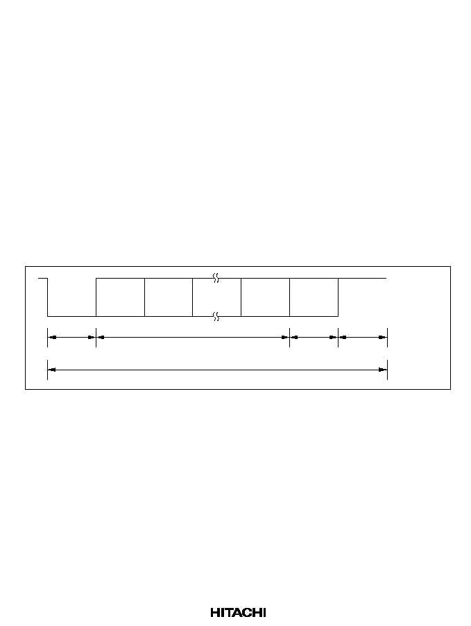
259
12.3.2
Asynchronous Mode
In asynchronous mode, each transmitted or received character is individually synchronized by
framing it with a start bit and stop bit.
Full duplex data transfer is possible because the SCI has independent transmit and receive
sections. Double buffering in both sections enables the SCI to be programmed for continuous data
transfer.
Figure 12.2 shows the general format of one character sent or received in asynchronous mode. The
communication channel is normally held in the mark state (high). Character transmission or
reception starts with a transition to the space state (low).
The first bit transmitted or received is the start bit (low). It is followed by the data bits, in which
the least significant bit (LSB) comes first. The data bits are followed by the parity or
multiprocessor bit, if present, then the stop bit or bits (high) confirming the end of the frame.
In receiving, the SCI synchronizes on the falling edge of the start bit, and samples each bit at the
center of the bit (at the 8th cycle of the internal serial clock, which runs at 16 times the bit rate).
D0
D1
Dn
Start bit
1 bit
7 or 8 bits
One unit of data (one character or frame)
Parity or
multipro-
cessor bit
Stop bit
0 or 1 bit
1 or 2 bits
Idle state
(mark)
Figure 12.2 Data Format in Asynchronous Mode
(Example of 8-Bit Data with Parity Bit and Two Stop Bits)
260
Data Format
Table 12.9 lists the data formats that can be sent and received in asynchronous mode. Twelve
formats can be selected by bits in the serial mode register (SMR).
Table 12.9
Data Formats in Asynchronous Mode
SMR Bits
CHR
PE
MP
STOP
1
2
3
4
5
6
7
8
9
10
11
12
0
0
0
0
S
8-bit data
STOP
0
0
0
1
S
8-bit data
STOP STOP
0
1
0
0
S
8-bit data
P
STOP
0
1
0
1
S
8-bit data
P
STOP STOP
1
0
0
0
S
7-bit data
STOP
1
0
0
1
S
7-bit data
STOP STOP
1
1
0
0
S
7-bit data
P
STOP
1
1
0
1
S
7-bit data
P
STOP STOP
0
--
1
0
S
8-bit data
MPB STOP
0
--
1
1
S
8-bit data
MPB STOP STOP
1
--
1
0
S
7-bit data
MPB STOP
1
--
1
1
S
7-bit data
MPB STOP STOP
Notes: SMR:
Serial mode register
S:
Start bit
STOP: Stop bit
P:
Parity bit
MPB:
Multiprocessor bit
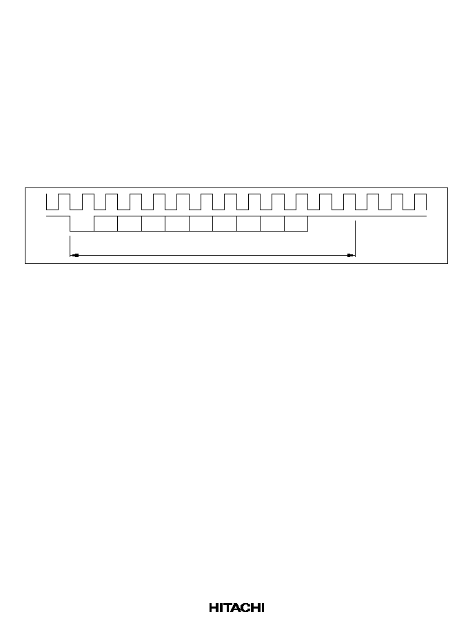
261
Clock
In asynchronous mode it is possible to select either an internal clock created by the on-chip baud
rate generator, or an external clock input at the SCK pin. The selection is made by the C/
A bit in
the serial mode register (SMR) and the CKE1 and CKE0 bits in the serial control register (SCR).
Refer to table 12.8.
If an external clock is input at the SCK pin, its frequency should be 16 times the desired bit rate.
If the internal clock provided by the on-chip baud rate generator is selected and the SCK pin is
used for clock output, the output clock frequency is equal to the bit rate, and the clock pulse rises
at the center of the transmit data bits. Figure 12.3 shows the phase relationship between the output
clock and transmit data.
0
D0
D1
D2
D3
D4
One frame
D5
D6
D7
0/1
1
1
Figure 12.3 Phase Relationship between Clock Output and Transmit Data
(Asynchronous Mode)
Transmitting and Receiving Data
SCI Initialization: Before transmitting or receiving, software must clear the TE and RE bits to 0
in the serial control register (SCR), then initialize the SCI following the procedure in figure 12.4.
Note:
When changing the communication mode or format, always clear the TE and RE bits to 0
before following the procedure given below. Clearing TE to 0 sets TDRE to 1 and
initializes the transmit shift register (TSR). Clearing RE to 0, however, does not initialize
the RDRF, PER, FER, and ORER flags and receive data register (RDR), which retain their
previous contents.
When an external clock is used, the clock should not be stopped during initialization or
subsequent operation. SCI operation becomes unreliable if the clock is stopped.
262
Clear TE and RE bits to
0 in SCR
1 bit interval
elapsed?
Start transmitting or receiving
No
Yes
1.
2.
3.
4.
Select interrupts and the clock source in the
serial control register (SCR). Leave TE and RE
cleared to 0. If clock output is selected, in
asynchronous mode, clock output starts
immediately after the setting is made in SCR.
Select the communication format in the serial
mode register (SMR).
Write the value corresponding to the bit rate in
the bit rate register (BRR). This step is not
necessary when an external clock is used.
Wait for at least the interval required to transmit
or receive one bit, then set TE or RE in the serial
control register (SCR). Setting TE or RE enables
the SCI to use the TxD or RxD pin.
Also set the RIE, TIE, TEIE, and MPIE bits as
necessary to enable interrupts. The initial states
are the mark transmit state, and the idle receive
state (waiting for a start bit).
1
2
Set CKE1 and CKE0 bits in
SCR (leaving TE and RE
cleared to 0)
3
Set TE or RE to 1 in SCR,
and set RIE, TIE, TEIE, and
MPIE as necessary
4
Initialization
Set value in BRR
Select communication
format in SMR
Figure 12.4 Sample Flowchart for SCI Initialization

263
Transmitting Serial Data: Follow the procedure in figure 12.5 for transmitting serial data.
Start transmitting
Read TDRE bit in SSR
TDRE = 1?
Write transmit data in TDR
End of
transmission?
End
1
2
3
No
Yes
No
Yes
SCI initialization: the transmit data output function
of the TxD pin is selected automatically.
After the TE bit is set to 1, one frame of 1s is output,
then transmission is possible.
SCI status check and transmit data write: read
the serial status register (SSR), check that the
TDRE bit is 1, then write transmit data in the
transmit data register (TDR) and clear TDRE to 0.
If a multiprocessor format is selected, after
writing the transmit data write 0 or 1 in the
multiprocessor bit transfer (MPBT) in SSR.
Transition of the TDRE bit from 0 to 1 can be
reported by an interrupt.
To continue transmitting serial data: read the
TDRE bit to check whether it is safe to write; if
TDRE = 1, write data in TDR, then clear TDRE
to 0.
To end serial transmission: end of transmission
can be confirmed by checking transition of the
TEND bit from 0 to 1. This can be reported by
a TEI interrupt.
To output a break signal at the end of serial
transmission: set the DDR bit to 1 and clear the
DR bit to 0 (DDR and DR are I/O port registers),
then clear TE to 0 in SCR.
(a)
(b)
If using multiprocessor format,
select MPBT value in SSR
Clear TDRE bit to 0
Read TEND bit in SSR
TEND = 1?
No
Yes
Output break
signal?
No
Yes
Clear TE bit in SCR to 0
4
1.
2.
3.
4.
Initialize
Set DR = 0, DDR = 1
Serial transmission
Figure 12.5 Sample Flowchart for Transmitting Serial Data

264
In transmitting serial data, the SCI operates as follows.
1. The SCI monitors the TDRE bit in SSR. When TDRE is cleared to 0 the SCI recognizes that
the transmit data register (TDR) contains new data, and loads this data from TDR into the
transmit shift register (TSR).
2. After loading the data from TDR into TSR, the SCI sets the TDRE bit to 1 and starts
transmitting. If the TIE bit (TDR-empty interrupt enable) is set to 1 in SCR, the SCI requests a
TXI interrupt (TDR-empty interrupt) at this time.
Serial transmit data are transmitted in the following order from the TxD pin:
a. Start bit: One 0 bit is output.
b. Transmit data: Seven or eight bits are output, LSB first.
c. Parity bit or multiprocessor bit: One parity bit (even or odd parity) or one multiprocessor
bit is output. Formats in which neither a parity bit nor a multiprocessor bit is output can
also be selected.
d. Stop bit: One or two 1 bits (stop bits) are output.
e. Mark state: Output of 1 bits continues until the start bit of the next transmit data.
3. The SCI checks the TDRE bit when it outputs the stop bit. If TDRE is 0, after loading new data
from TDR into TSR and transmitting the stop bit, the SCI begins serial transmission of the next
frame. If TDRE is 1, after setting the TEND bit to 1 in SSR and transmitting the stop bit, the
SCI continues 1-level output in the mark state, and if the TEIE bit (TSR-empty interrupt
enable) in SCR is set to 1, the SCI generates a TEI interrupt request (TSR-empty interrupt).
Figure 12.6 shows an example of SCI transmit operation in asynchronous mode.

265
1
Start
bit
0
D0
D1
D7
0/ 1
Stop
bit
1
Data
Parity
bit
Start
bit
0
D0
D1
D7
0/ 1
Stop
bit
1
Data
Parity
bit
1
Idle state
(mark)
TDRE
TEND
TXI
request
TXI interrupt handler
writes data in TDR and
clears TDRE to 0
TXI
request
1 frame
TEI request
Figure 12.6 Example of SCI Transmit Operation
(8-Bit Data with Parity and One Stop Bit)
266
Receiving Serial Data: Follow the procedure in figure 12.7 for receiving serial data.
Start receiving
RDRF = 1?
Read receive data from RDR,
and clear RDRF bit to 0
in SSR
PER
RER
ORER = 1?
Clear RE to 0 in SCR
Finished
receiving?
End
Error handling
Start error handling
FER = 1?
Discriminate and
process error, and
clear flags
Return
Break?
Clear RE to 0
in SCR
End
1
2
No
Yes
Yes
No
No
Yes
4
1.
2.
3.
4.
SCI initialization: the receive data function of the RxD
pin is selected automatically.
To continue receiving serial data: read RDR and
clear RDRF to 0 before the stop bit of the current
frame is received.
SCI status check and receive data read: read the
serial status register (SSR), check that RDRF is set
to 1, then read receive data from the receive data
register (RDR) and clear RDRF to 0. Transition of
the RDRF bit from 0 to 1 can be reported by an RXI
interrupt.
Receive error handling and break detection: if a
receive error occurs, read the ORER, PER, and
FER bits in SSR to identify the error. After executing
the necessary error handling, clear ORER, PER, and
FER all to 0. Transmitting and receiving cannot
resume if ORER, PER, or FER remains set to 1.
When a framing error occurs, the RxD pin can be
read to detect the break state.
Yes
No
Yes
No
3
Initialize
Read ORER, PER, and
FER in SSR
Read RDRF bit in SSR
Figure 12.7 Sample Flowchart for Receiving Serial Data

267
In receiving, the SCI operates as follows.
1. The SCI monitors the receive data line and synchronizes internally when it detects a start bit.
2. Receive data is shifted into RSR in order from LSB to MSB.
3. The parity bit and stop bit are received.
After receiving these bits, the SCI makes the following checks:
a. Parity check: The number of 1s in the receive data must match the even or odd parity
setting of the O/
E bit in SMR.
b. Stop bit check: The stop bit value must be 1. If there are two stop bits, only the first stop bit
is checked.
c. Status check: RDRF must be 0 so that receive data can be loaded from RSR into RDR.
If these checks all pass, the SCI sets RDRF to 1 and stores the received data in RDR. If one of
the checks fails (receive error), the SCI operates as indicated in table 12.10.
Note:
When a receive error flag is set, further receiving is disabled. The RDRF bit is not set
to 1. Be sure to clear the error flags.
4. After setting RDRF to 1, if the RIE bit (receive-end interrupt enable) is set to 1 in SCR, the
SCI requests an RXI (receive-end) interrupt. If one of the error flags (ORER, PER, or FER) is
set to 1 and the RIE bit in SCR is also set to 1, the SCI requests an ERI (receive-error)
interrupt.
Figure 12.8 shows an example of SCI receive operation in asynchronous mode.
Table 12.10 Receive Error Conditions and SCI Operation
Receive error
Abbreviation
Condition
Data Transfer
Overrun error
ORER
Receiving of next data ends
while RDRF is still set to 1 in
SSR
Receive data not loaded from
RSR into RDR
Framing error
FER
Stop bit is 0
Receive data loaded from
RSR into RDR
Parity error
PER
Parity of receive data differs
from even/odd parity setting
in SMR
Receive data loaded from
RSR into RDR

268
1
Start
bit
0
D0
D1
D7
0/ 1
Stop
bit
1
Data
Parity
bit
Start
bit
0
D0
D1
D7
0/ 1
Stop
bit
0
Data
Parity
bit
1
Idle state
(mark)
RDRF
FER
1 frame
Framing error,
ERI request
RXI interrupt handler
reads data in RDR and
clears RDRF to 0
RXI
request
Figure 12.8 Example of SCI Receive Operation (8-Bit Data with Parity and One Stop Bit)
Multiprocessor Communication
The multiprocessor communication function enables several processors to share a single serial
communication line. The processors communicate in asynchronous mode using a format with an
additional multiprocessor bit (multiprocessor format).
In multiprocessor communication, each receiving processor is addressed by an ID.
A serial communication cycle consists of two cycles: an ID-sending cycle that identifies the
receiving processor, and a data-sending cycle. The multiprocessor bit distinguishes ID-sending
cycles from data-sending cycles.
The transmitting processor starts by sending the ID of the receiving processor with which it wants
to communicate as data with the multiprocessor bit set to 1. Next the transmitting processor sends
transmit data with the multiprocessor bit cleared to 0.
Receiving processors skip incoming data until they receive data with the multiprocessor bit set to
1.
After receiving data with the multiprocessor bit set to 1, the receiving processor with an ID
matching the received data continues to receive further incoming data. Multiple processors can
send and receive data in this way.
Four formats are available. Parity-bit settings are ignored when a multiprocessor format is
selected. For details see table 12.9.
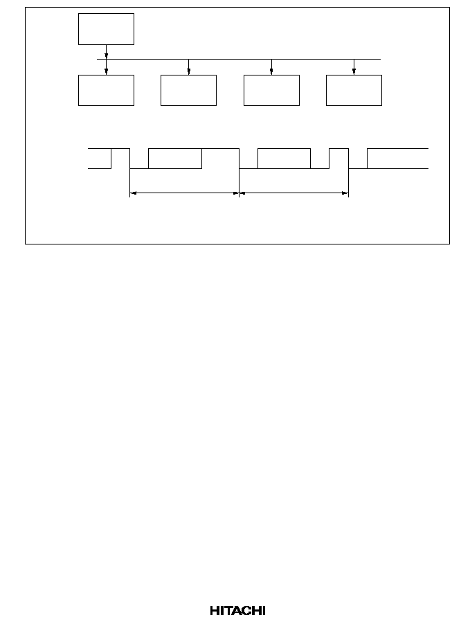
269
Transmitting
processor
Receiving
processor A
Serial communication line
Receiving
processor B
Receiving
processor C
Receiving
processor D
(ID = 01)
(ID = 02)
(ID = 03)
(ID = 04)
Serial data
H'01
H'AA
(MPB = 1)
(MPB = 0)
ID-sending cycle:
receiving processor address
Data-sending cycle:
data sent to receiving
processor specified by ID
MPB: Multiprocessor bit
Figure 12.9 Example of Communication among Processors using Multiprocessor Format
(Sending Data H'AA to Receiving Processor A)

270
Transmitting Multiprocessor Serial Data: See figures 12.5 and 12.6.
Receiving Multiprocessor Serial Data: Follow the procedure in figure 12.10 for receiving
multiprocessor serial data.
Start receiving
Set MPIE bit to 1 in SCR
FER
ORER = 1?
FER +
ORER = 1?
Finished
receiving?
Clear RE to 0 in SCR
End
Error handling
FER = 1?
Discriminate and
process error, and
clear flags
Return
Break?
Clear RE bit to
0 in SCR
End
1
2
3
4
No
Yes
Yes
No
Yes
No
No
Yes
No
Yes
5
1.
SCI initialization: the receive data function of the RxD pin is
selected automatically.
2.
ID receive cycle: Set the MPIE bit in the serial control register
(SCR) to 1.
3.
SCI status check and ID check: read the serial status register
(SSR), check that RDRF is set to 1, then read receive data
from the receive data register (RDR) and compare with the
processor's own ID. Transition of the RDRF bit from 0 to
1 can be reported by an RXI interrupt. If the ID does not match
the receive data, set MPIE to 1 again and clear RDRF to 0.
If the ID matches the receive data, clear RDRF to 0.
4.
SCI status check and data receiving: read SSR, check that
RDRF is set to 1, then read data from the receive data register
(RDR) and write 0 in the RDRF bit. Transition of the RDRF bit
from 0 to 1 can be reported by an RXI interrupt.
5.
Receive error handling and break detection: if a receive error
occurs, read the ORER and FER bits in SSR to identify the error.
After executing the necessary error handling, clear both ORER
and FER to 0. Receiving cannot resume while ORER or FER
remains set to 1. When a framing error occurs, the RxD pin
can be read to detect the break state.
Yes
No
Yes
No
Initialize
Start error handling
Read RDRF bit in SSR
RDRF = 1?
Read ORER and FER
bits in SSR
Own ID?
No
Yes
Read RDRF bit in SSR
RDRF = 1?
Read ORER and FER
bits in SSR
Read receive data from RDR
Read receive data from RDR
Figure 12.10 Sample Flowchart for Receiving Multiprocessor Serial Data
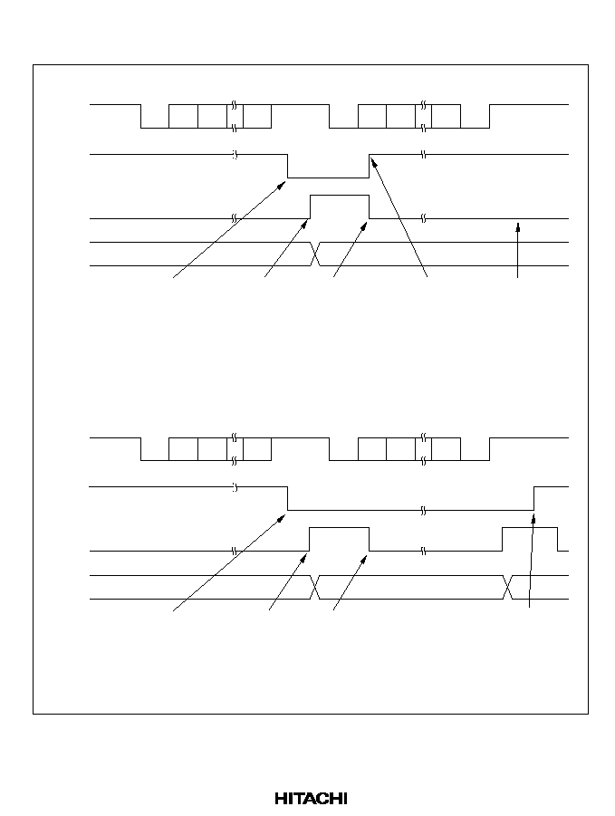
271
Figure 12.11 shows an example of an SCI receive operation using a multiprocessor format (8-bit
data with multiprocessor bit and one stop bit).
1
Start
bit
0
D0
D1
D7
1
Stop
bit
1
Data (ID1)
MPB
Start
bit
0
D0
D1
D7
0
Stop
bit
1
Data (Data1)
MPB
1
Idle state
(mark)
MPIE
RDRF
RDR value
ID1
RXI request
RXI handler reads
RDR data and clears
RDRF to 0
Not own ID, so
MPIE is set to
1 again
No RXI request,
RDR not updated
(Multiprocessor interrupt)
(a) Own ID does not match data
1
Start
bit
0
D0
D1
D7
1
Stop
bit
1
Data (ID2)
MPB
Start
bit
0
D0
D1
D7
0
Stop
bit
1
Data (Data2)
MPB
1
Idle state
(mark)
MPIE
RDRF
RDR value
ID2
RXI handler reads
RDR data and clears
RDRF to 0
Own ID, so receiving
continues, with data
received at each RXI
MPIE set to
1 again
(Multiprocessor interrupt)
(b) Own ID matches data
Data 2
MPB detection
MPIE = 0
RXI request
MPB detection
MPIE = 0
Figure 12.11 Example of SCI Receive Operation
(8-Bit Data with Multiprocessor Bit and One Stop Bit)

272
12.3.3
Synchronous Mode
Overview
In synchronous mode, the SCI transmits and receives data in synchronization with clock pulses.
This mode is suitable for high-speed serial communication.
The SCI transmitter and receiver share the same clock but are otherwise independent, so full
duplex communication is possible. The transmitter and receiver are also double buffered, so
continuous transmitting or receiving is possible by reading or writing data while transmitting or
receiving is in progress.
Figure 12.12 shows the general format in synchronous serial communication.
Serial clock
Serial data
Bit 0
Bit 1
Bit 2
Bit 3
Bit 4
Bit 5
Bit 6
Bit 7
LSB
MSB
Don't care
Don't care
One unit (character or frame) of serial data
*
*
Note: High except in continuous transmitting or receiving
*
Figure 12.12 Data Format in Synchronous Communication
In synchronous serial communication, each data bit is sent on the communication line from one
falling edge of the serial clock to the next. Data is received in synchronization with the rising edge
of the serial clock.
In each character, the serial data bits are transmitted in order from LSB (first) to MSB (last). After
output of the MSB, the communication line remains in the state of the MSB.
Communication Format: The data length is fixed at eight bits. No parity bit or multiprocessor bit
can be added.
Clock: An internal clock generated by the on-chip baud rate generator or an external clock input
from the SCK pin can be selected by clearing or setting the C/
A
bit in the serial mode register
(SMR) and the CKE1 and CKE0 bits in the serial control register (SCR). See table 12.8.
When the SCI operates on an internal clock, it outputs the clock signal at the SCK pin. Eight clock
pulses are output per transmitted or received character. When the SCI is not transmitting or
receiving, the clock signal remains at the high level.
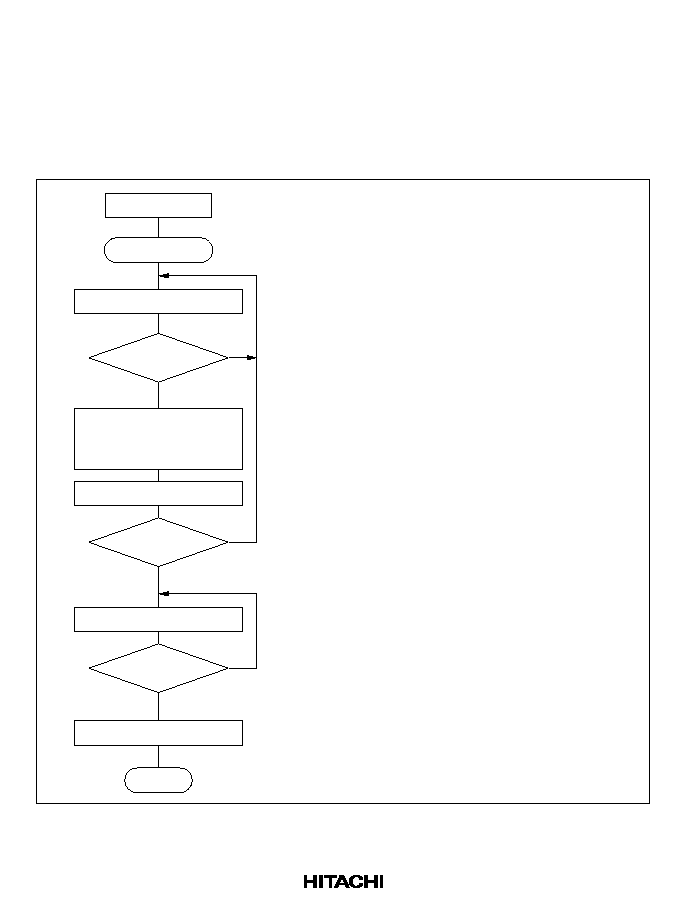
273
Transmitting and Receiving Data
SCI Initialization: The SCI must be initialized in the same way as in asynchronous mode. See
figure 12.4. When switching from asynchronous mode to synchronous mode, check that the
ORER, FER, and PER bits are cleared to 0. Transmitting and receiving cannot begin if ORER,
FER, or PER is set to 1.
Transmitting Serial Data: Follow the procedure in figure 12.13 for transmitting serial data.
Start transmitting
Read TDRE bit in SSR
TDRE = 1?
Write transmit data in
TDR and clear TDRE bit to
0 in SSR
End of
transmission?
End
1
2
3
No
Yes
No
Yes
SCI initialization: the transmit data output function
of the TxD pin is selected automatically.
SCI status check and transmit data write: read
the serial status register (SSR), check that the
TDRE bit is 1, then write transmit data in the
transmit data register (TDR) and clear TDRE to 0.
Transition of the TDRE bit from 0 to 1 can be
reported by a TXI interrupt.
To continue transmitting serial data: read the
TDRE bit to check whether it is safe to write; if
TDRE = 1, write data in TDR, then clear TDRE
to 0.
To end serial transmission: end of transmission
can be confirmed by checking transition of the
TEND bit from 0 to 1. This can be reported by
a TEI interrupt.
(a)
(b)
Read TEND bit in SSR
TEND = 1?
No
Yes
1.
2.
3.
Initialize
Clear TE bit to 0 in SCR
Serial transmission
Figure 12.13 Sample Flowchart for Serial Transmitting
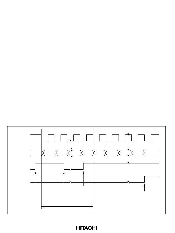
274
In transmitting serial data, the SCI operates as follows.
1. The SCI monitors the TDRE bit in SSR. When TDRE is cleared to 0 the SCI recognizes that
the transmit data register (TDR) contains new data, and loads this data from TDR into the
transmit shift register (TSR).
2. After loading the data from TDR into TSR, the SCI sets the TDRE bit to 1 and starts
transmitting. If the TIE bit (TDR-empty interrupt enable) in SCR is set to 1, the SCI requests a
TXI interrupt (TDR-empty interrupt) at this time.
If clock output is selected the SCI outputs eight serial clock pulses, triggered by the clearing of
the TDRE bit to 0. If an external clock source is selected, the SCI outputs data in
synchronization with the input clock.
Data is output from the TxD pin in order from LSB (bit 0) to MSB (bit 7).
3. The SCI checks the TDRE bit when it outputs the MSB (bit 7). If TDRE is 0, the SCI loads
data from TDR into TSR, then begins serial transmission of the next frame. If TDRE is 1, the
SCI sets the TEND bit in SSR to 1, transmits the MSB, then holds the output in the MSB state.
If the TEIE bit (transmit-end interrupt enable) in SCR is set to 1, a TEI interrupt (TSR-empty
interrupt) is requested at this time.
4. After the end of serial transmission, the SCK pin is held at the high level.
Figure 12.14 shows an example of SCI transmit operation.
Serial clock
Serial data
Bit 0
Bit 1
Bit 7
Bit 0
Bit 1
Bit 6
Bit 7
TXI
request
TDRE
TEND
TXI interrupt
handler writes
data in TDR and
clears TDRE to 0
TXI
request
TEI
request
1 frame
Figure 12.14 Example of SCI Transmit Operation
275
Receiving Serial Data: Follow the procedure in figure 12.15 for receiving serial data. When
switching from asynchronous mode to synchronous mode, be sure to check that PER and FER are
cleared to 0. If PER or FER is set to 1 the RDRF bit will not be set and both transmitting and
receiving will be disabled.
Start receiving
Read ORER bit in SSR
ORER = 1?
RDRF = 1?
Read RDRF in SSR
Finished
receiving?
Clear RE to 0 in SCR
End
Error handling
1
2
3
Yes
No
No
Yes
No
Yes
4
1.
2.
3.
4.
SCI initialization: the receive data function of the
RxD pin is selected automatically.
Receive error handling: if a receive error occurs,
read the ORER bit in SSR then, after executing
the necessary error handling, clear ORER to 0.
Neither transmitting nor receiving can resume
while ORER remains set to 1. When clock
output mode is selected, receiving can be halted
temporarily by receiving one dummy byte and
causing an overrun error. When preparations
to receive the next data are completed, clear
the ORER bit to 0. This causes receiving to
resume, so return to the step marked 2 in the
flowchart.
SCI status check and receive data read: read
the serial status register (SSR), check that
RDRF is set to 1, then read receive data from
the receive data register (RDR) and clear RDRF
to 0. Transition of the RDRF bit from 0 to 1
can be reported by an RXI interrupt.
To continue receiving serial data: read RDR and
clear RDRF to 0 before the MSB (bit 7) of the
current frame is received.
Clear ORER to 0 in SSR
Return
Overrun error handling
Start error handling
Initialize
Read receive data
from RDR, and clear
RDRF bit to 0 in SSR
Figure 12.15 Sample Flowchart for Serial Receiving
276
In receiving, the SCI operates as follows.
1. If an external clock is selected, data is input in synchronization with the input clock. If clock
output is selected, as soon as the RE bit is set to 1 the SCI begins outputting the serial clock
and inputting data. If clock output is stopped because the ORER bit is set to 1, output of the
serial clock and input of data resume as soon as the ORER bit is cleared to 0.
2. Receive data is shifted into RSR in order from LSB to MSB.
After receiving the data, the SCI checks that RDRF is 0 so that receive data can be loaded from
RSR into RDR. If this check passes, the SCI sets RDRF to 1 and stores the received data in
RDR. If the check does not pass (receive error), the SCI operates as indicated in
table 12.10.
Note:
Both transmitting and receiving are disabled while a receive error flag is set. The
RDRF bit is not set to 1. Be sure to clear the error flag.
3. After setting RDRF to 1, if the RIE bit (receive-end interrupt enable) is set to 1 in SCR, the
SCI requests an RXI (receive-end) interrupt. If the ORER bit is set to 1 and the RIE bit in SCR
is set to 1, the SCI requests an ERI (receive-error) interrupt.
When clock output mode is selected, clock output stops when the RE bit is cleared to 0 or the
ORER bit is set to 1. To prevent clock count errors, it is safest to receive one dummy byte and
generate an overrun error.
Figure 12.16 shows an example of SCI receive operation.
Serial clock
Serial data
Bit 0
Bit 1
Bit 7
Bit 0
Bit 1
Bit 6
Bit 7
RXI
request
RDRF
ORER
RXI interrupt
handler reads
data in RDR and
clears RDRF to 0
RXI
request
Overrun error,
ERI request
1 frame
Figure 12.16 Example of SCI Receive Operation

277
Transmitting and Receiving Serial Data Simultaneously: Follow the procedure in figure
12.17 for transmitting and receiving serial data simultaneously. If clock output mode is selected,
output of the serial clock begins simultaneously with serial transmission.
Start
Read TDRE bit in SSR
TDRE = 1?
Write transmit data
in TDR and clear TDRE
bit to 0 in SSR
RDRF = 1?
Read ORER bit in SSR
End of
transmitting and
receiving?
Clear TE and RE bits
to 0 in SCR
End
Error handling
1
2
3
No
Yes
Yes
Yes
No
Yes
4
1.
2.
3.
4.
5.
SCI initialization: the transmit data output function of
the TxD pin and receive data input function of the
RxD pin are selected, enabling simultaneous
transmitting and receiving.
SCI status check and transmit data write: read the
serial status register (SSR), check that the TDRE bit
is 1, then write transmit data in the transmit data
register (TDR) and clear TDRE to 0. Transition of the
TDRE bit from 0 to 1 can be reported by a TXI interrupt.
SCI status check and receive data read: read the
serial status register (SSR), check that the RDRF
bit is 1, then read receive data from the receive data
register (RDR) and clear RDRF to 0. Transition of
the RDRF bit from 0 to 1 can be reported by an RXI
interrupt.
Receive error handling: if a receive error occurs, read
the ORER bit in SSR then, after executing the
necessary error handling, clear ORER to 0. Neither
transmitting nor receiving can resume while ORER
remains set to 1.
To continue transmitting and receiving serial data:
read RDR and clear RDRF to 0 before the MSB
(bit 7) of the current frame is received. Also read the
TDRE bit and check that it is set to 1, indicating that
it is safe to write; then write data in TDR and clear
TDRE to 0 before the MSB (bit 7) of the current frame
is transmitted.
ORER = 1?
Read RDRF bit in SSR
5
No
No
Initialize
Read receive data
from RDR and clear
RDRF bit to 0 in SSR
Figure 12.17 Sample Flowchart for Serial Transmitting and Receiving
Note:
In switching from transmitting or receiving to simultaneous transmitting and receiving,
clear both TE and RE to 0, then set TE and RE to 1 simultaneously using an MOV
instruction. Do not use a BEST instruction for this purpose.

278
12.4
Interrupts
The SCI can request four types of interrupts: ERI, RXI, TXI, and TEI. Table 12.11 indicates the
source and priority of these interrupts. The interrupt sources can be enabled or disabled by the
TIE, RIE, and TEIE bits in the SCR. Independent signals are sent to the interrupt controller for
each interrupt source, except that the receive-error interrupt (ERI) is the logical OR of three
sources: overrun error, framing error, and parity error.
The TXI interrupt indicates that the next transmit data can be written. The TEI interrupt indicates
that the SCI has stopped transmitting data.
Table 12.11 SCI Interrupt Sources
Interrupt
Description
Priority
ERI
Receive-error interrupt (ORER, FER, or PER)
High
RXI
Receive-end interrupt (RDRF)
TXI
TDR-empty interrupt (TDRE)
TEI
TSR-empty interrupt (TEND)
Low
12.5
Application Notes
Application programmers should note the following features of the SCI.
TDR Write: The TDRE bit in SSR is simply a flag that indicates that the TDR contents have been
transferred to TSR. The TDR contents can be rewritten regardless of the TDRE value. If a new
byte is written in TDR while the TDRE bit is 0, before the old TDR contents have been moved
into TSR, the old byte will be lost. Software should check that the TDRE bit is set to 1 before
writing to TDR.
Multiple Receive Errors: Table 12.12 lists the values of flag bits in the SSR when multiple
receive errors occur, and indicates whether the RSR contents are transferred to RDR.

279
Table 12.12
SSR Bit States and Data Transfer when Multiple Receive Errors Occur
SSR Bits
RSR
Receive error
RDRF
ORER
FER
PER
RDR
*
2
Overrun error
1
*
1
1
0
0
No
Framing error
0
0
1
0
Yes
Parity error
0
0
0
1
Yes
Overrun and framing errors
1
*
1
1
1
0
No
Overrun and parity errors
1
*
1
1
0
1
No
Framing and parity errors
0
0
1
1
Yes
Overrun, framing, and parity errors
1
*
1
1
1
1
No
Notes:
*
1 Set to 1 before the overrun error occurs.
*
2 Yes: The RSR contents are transferred to RDR.
No: The RSR contents are not transferred to RDR.
Line Break Detection: When the RxD pin receives a continuous stream of 0's in asynchronous
mode (line-break state), a framing error occurs because the SCI detects a 0 stop bit. The value
H'00 is transferred from RSR to RDR. Software can detect the line-break state as a framing error
accompanied by H'00 data in RDR.
The SCI continues to receive data, so if the FER bit is cleared to 0 another framing error will
occur.
Sampling Timing and Receive Margin in Asynchronous Mode: The serial clock used by the
SCI in asynchronous mode runs at 16 times the bit rate. The falling edge of the start bit is detected
by sampling the RxD input on the falling edge of this clock. After the start bit is detected, each bit
of receive data in the frame (including the start bit, parity bit, and stop bit or bits) is sampled on
the rising edge of the serial clock pulse at the center of the bit. See figure 12.18.
It follows that the receive margin can be calculated as in equation (1).
When the absolute frequency deviation of the clock signal is 0 and the clock duty cycle is 0.5, data
can theoretically be received with distortion up to the margin given by equation (2). This is a
theoretical limit, however. In practice, system designers should allow a margin of 20% to 30%.
280
1 2
4
0
5 6 7 8 9
3
2
1 2 3 4 5 6 7 8 9
1
11 12
1314 15 16
10
13 14 1516
12
10 11
3 4 5
Basic
clock
Sync
sampling
Data
sampling
D0
D1
Receive
data
Start bit
≠7.5 pulses
+7.5 pulses
Figure 12.18 Sampling Timing (Asynchronous Mode)
M = {(0.5 ≠ 1/2N) ≠ (D ≠ 0.5)/N ≠ (L ≠ 0.5)F}
◊
100 [%] .................................... (1)
M: Receive margin
N: Ratio of basic clock to bit rate (N=16)
D: Duty factor of clock--ratio of high pulse width to low width (0.5 to 1.0)
L: Frame length (9 to 12)
F: Absolute clock frequency deviation
When D = 0.5 and F = 0
M = (0.5 ≠1/2
◊
16)
◊
100 [%] = 46.875% ......................................................... (2)

281
Section 13 I
2
C Bus Interface (H8/3337 Series Only)
[Option]
An I
2
C bus interface is available as an option. Observe the following notes when using this option.
∑
For mask-ROM versions, the Y in the part number becomes a W in products in which this
optional function is used.
Examples: HD6433337WF, HD6433334WF
13.1
Overview
The I
2
C bus interface conforms to and provides a subset of the Philips I
2
C bus (inter-IC bus)
interface functions. The register configuration that controls the I
2
C bus differs partly from the
Philips configuration, however.
The I
2
C bus interface uses only one data line (SDA) and one clock line (SCL) to transfer data, so it
can save board and connector space. Figure 13.1 shows typical I
2
C bus interface connections.
13.1.1
Features
∑
Conforms to Philips I
2
C bus interface
∑
Start and stop conditions generated automatically
∑
Selectable acknowledge output level when receiving
∑
Auto-loading of acknowledge bit when transmitting
∑
Selection of eight internal clocks (in master mode)
∑
Selection of acknowledgement mode, or serial mode without acknowledge bit
∑
Wait function: a wait can be inserted in acknowledgement mode by holding the SCL pin low
after a data transfer, before acknowledgement of the transfer.
∑
Three interrupt sources
Data transfer end
In slave receive mode: slave address matched, or general call address received
In master transmit mode: bus arbitration lost
∑
Direct bus drive (with pins SCL and SDA)
∑
The P8
6
/SCK
1
/SCL pin and the P9
7
/
WAIT/SDA pin are NMOS outputs only when the bus
drive function is selected

282
SCL in
SCL out
SDA in
SDA out
(Slave 1)
SCL
SDA
SCL in
SCL out
SDA in
SDA out
(Slave 2)
SCL
SDA
SCL in
SCL out
SDA in
SDA out
(Master)
SCL
SDA
V
CC
SCL
SDA
Figure 13.1 I
2
C Bus Interface Connections (Example) (H8/3337 Series Chip as Master)

283
13.1.2
Block Diagram
Figure 13.2 shows a block diagram of the I
2
C bus interface.
¯
P
PS
Noise
canceler
Noise
canceler
Clock
control
Bus state
decision
circuit
Arbitration
decision
circuit
Output data
control
circuit
Address
comparator
SAR
Interrupt
generator
ICDR
ICSR
ICMR
ICCR
STCR
Internal data bus
Interrupt
request
SCL
SDA
Legend:
ICCR:
ICMR:
ICSR:
ICDR:
SAR:
PS:
STCR:
I
2
C bus control register
I
2
C bus mode register
I
2
C bus status register
I
2
C bus data register
Slave address register
Prescaler
Serial timer control register
Figure 13.2 Block Diagram of I
2
C Bus Interface

284
13.1.3
Input/Output Pins
Table 13.1 summarizes the input/output pins used by the I
2
C bus interface.
Table 13.1
I
2
C Bus Interface
Name
Abbreviation
I/O
Function
Serial clock
SCL
Input/output
Serial clock input/output
Serial data
SDA
Input/output
Serial data input/output
13.1.4
Register Configuration
Table 13.2 summarizes the registers of the I
2
C bus interface.
Table 13.2
I
2
C Bus Interface Register Configuration
Name
Abbreviation
R/W
Initial Value
Address
*
2
I
2
C bus control register
ICCR
R/W
H'00
H'FFD8
I
2
C bus status register
ICSR
R/W
H'30
H'FFD9
I
2
C bus data register
ICDR
R/W
--
H'FFDE
I
2
C bus mode register
ICMR
R/W
H'38
H'FFDF
*
1
Slave address register
SAR
R/W
H'00
H'FFDF
*
1
Serial timer control register
STCR
R/W
H'00
H'FFC3
Notes:
*
1 The register that can be written or read depends on the ICE bit in the I
2
C bus control
register. The slave address register can be accessed when ICE = 0. The I
2
C bus mode
register can be accessed when ICE = 1.
*
2 The addresses assigned to the I
2
C bus interface registers are also assigned to other
registers. The accessible registers are selected with bit IICE in the serial/timer control
register (STCR).

285
13.2
Register Descriptions
13.2.1
I
2
C Bus Data Register (ICDR)
Bit
7
6
5
4
3
2
1
0
ICDR7
ICDR6
ICDR5
ICDR4
ICDR3
ICDR2
ICDR1
ICDR0
Initial value
--
--
--
--
--
--
--
--
Read/Write
R/W
R/W
R/W
R/W
R/W
R/W
R/W
R/W
ICDR is an 8-bit readable/writable register that is used as a transmit data register when
transmitting and a receive data register when receiving. Transmitting is started by writing data in
ICDR. Receiving is started by reading data from ICDR.
ICDR is also used as a shift register, so it must not be written or read until data has been
completely transmitted or received. Read or write access while data is being transmitted or
received may result in incorrect data.
The ICDR value is undefined after a reset and in hardware standby mode.
13.2.2
Slave Address Register (SAR)
Bit
7
6
5
4
3
2
1
0
SVA6
SVA5
SVA4
SVA3
SVA2
SVA1
SVA0
FS
Initial value
0
0
0
0
0
0
0
0
Read/Write
R/W
R/W
R/W
R/W
R/W
R/W
R/W
R/W
SAR is an 8-bit readable/writable register that stores the slave address and selects the
communication format. When the chip is in slave mode (and the addressing format is selected), if
the upper 7 bits of SAR match the upper 7 bits of the first byte received after a start condition, the
chip operates as the slave device specified by the master device. SAR is assigned to the same
address as ICMR. SAR can be written and read only when the ICE bit is cleared to 0 in ICCR.
SAR is initialized to H'00 by a reset and in hardware standby mode.
Bits 7 to 1--Slave Address (SVA6 to SVA0): Set a unique address in bits SVA6 to SVA0,
differing from the addresses of other slave devices connected to the I
2
C bus.

286
Bit 0--Format Select (FS): Selects whether to use the addressing format or non-addressing
format in slave mode. The addressing format is used to recognize slave addresses.
Bit 0: FS
Description
0
Addressing format, slave addresses recognized
(Initial value)
1
Non-addressing format
13.2.3
I
2
C Bus Mode Register (ICMR)
Bit
7
6
5
4
3
2
1
0
MLS
WAIT
--
--
--
BC2
BC1
BC0
Initial value
0
0
1
1
1
0
0
0
Read/Write
R/W
R/W
--
--
--
R/W
R/W
R/W
ICMR is an 8-bit readable/writable register that selects whether the MSB or LSB is transferred
first, performs wait control, and selects the transfer bit count. ICMR is assigned to the same
address as SAR. ICMR can be written and read only when the ICE bit is set to 1 in ICCR.
ICMR is initialized to H'38 by a reset and in hardware standby mode.
Bit 7--MSB-First/LSB-First Select (MLS): Selects whether data is transferred MSB-first or
LSB-first.
Bit 7: MLS
Description
0
MSB-first
(Initial value)
1
LSB-first
Bit 6--Wait Insertion Bit (WAIT): Selects whether to insert a wait between the transfer of data
and the acknowledge bit, in acknowledgement mode. When WAIT is set to 1, after the fall of the
clock for the final data bit, a wait state begins (with SCL staying at the low level). When bit IRIC
is cleared in ICSR, the wait ends and the acknowledge bit is transferred. If WAIT is cleared to 0,
data and acknowledge bits are transferred consecutively with no wait inserted.
Bit 6: WAIT
Description
0
Data and acknowledge transferred consecutively
(Initial value)
1
Wait inserted between data and acknowledge
287
Bits 5 to 3--Reserved: These bits cannot be modified and are always read as 1.
Bits 2 to 0--Bit Counter (BC2 to BC0): BC2 to BC0 specify the number of bits to be transferred
next. When the ACK bit is cleared to 0 in ICCR (acknowledgement mode), the data is transferred
with one additional acknowledge bit. BC2 to BC0 settings should be made during an interval
between transfer frames. If BC2 to BC0 are set to a value other than 000, the setting should be
made while the SCL line is low.
The bit counter is initialized to 000 by a reset and when a start condition is detected. The value
returns to 000 at the end of a data transfer, including the acknowledge.
Bit 2:
Bit 1:
Bit 0:
Bits/Frame
BC2
BC1
BC0
Serial Mode
Acknowledgement Mode
0
0
0
8
9
(Initial value)
1
1
2
1
0
2
3
1
3
4
1
0
0
4
5
1
5
6
1
0
6
7
1
7
8
13.2.4
I
2
C Bus Control Register (ICCR)
Bit
7
6
5
4
3
2
1
0
ICE
IEIC
MST
TRS
ACK
CKS2
CKS1
CKS0
Initial value
0
0
0
0
0
0
0
0
Read/Write
R/W
R/W
R/W
R/W
R/W
R/W
R/W
R/W
ICCR is an 8-bit readable/writable register that enables or disables the I
2
C bus interface, enables or
disables interrupts, and selects master or slave mode, transmit or receive, acknowledgement or
serial mode, and the clock frequency.
ICCR is initialized to H'00 by a reset and in hardware standby mode.
Bit 7--I
2
C Bus Interface Enable (ICE): Selects whether or not to use the I
2
C bus interface.
When ICE is set to 1, the SCL and SDA signals are assigned to input/output pins and transfer
operations are enabled. When ICE is cleared to 0, SCL and SDA are placed in the high-impedance
state and the interface module is disabled.

288
The SAR register can be accessed when ICE is 0. The ICMR register can be accessed when ICE is
1.
Bit 7: ICE
Description
0
Interface module disabled, with SCL and SDA signals in high-impedance state
(Initial value)
1
Interface module enabled for transfer operations (pins SCL and SCA are
driving the bus
*
)
Note:
*
Pin SDA is multiplexed with the
WAIT
input pin. In expanded mode,
WAIT
input has priority
for this pin.
Bit 6--I
2
C Bus Interface Interrupt Enable (IEIC): Enables or disables interrupts from the I
2
C
bus interface to the CPU.
Bit 6: IEIC
Description
0
Interrupts disabled
(Initial value)
1
Interrupts enabled
Bit 5--Master/Slave Select (MST)
Bit 4--Transmit/Receive Select (TRS)
MST selects whether the I
2
C bus interface operates in master mode or slave mode.
TRS selects whether the I
2
C bus interface operates in transmit mode or receive mode.
In master mode, when arbitration is lost, MST and TRS are both reset by hardware, causing a
transition to slave receive mode. In slave receive mode with the addressing format (FS = 0),
hardware automatically selects transmit or receive mode according to the R/W bit in the first byte
after a start condition.
MST and TRS select the operating mode as follows.
Bit 5: MST
Bit 4: TRS
Description
0
0
Slave receive mode
(Initial value)
1
Slave transmit mode
1
0
Master receive mode
1
Master transmit mode

289
Bit 3--Acknowledgement Mode Select (ACK): Selects acknowledgement mode or serial mode.
In acknowledgement mode (ACK = 0), data is transferred in frames consisting of the number of
data bits selected by BC2 to BC0 in ICMR, plus an extra acknowledge bit. In serial mode (ACK =
1), the number of data bits selected by BC2 to BC0 in ICMR is transferred as one frame.
Bit 3: ACK
Description
0
Acknowledgement mode
(Initial value)
1
Serial mode
Bits 2 to 0--Serial Clock Select (CKS2 to CKS0): These bits, together with the IICX bit in the
STCR register, select the serial clock frequency in master mode. They should be set according to
the required transfer rate.
(STCR)
Bit 2:
Bit 1:
Bit 0:
Transfer Rate
*
IICX
CKS2
CKS1
CKS0
Clock
¯
P
= 5 MHz
¯
P
= 8 MHz
¯
P
= 10 MHz ¯
P
= 16 MHz
0
0
0
0
¯
P
/28
179 kHz
286 kHz
357 kHz
571 kHz
1
¯
P
/40
125 kHz
200 kHz
250 kHz
400 kHz
1
0
¯
P
/48
104 kHz
167 kHz
208 kHz
333 kHz
1
¯
P
/64
78.1 kHz
125 kHz
156 kHz
250 kHz
1
0
0
¯
P
/80
62.5 kHz
100 kHz
125 kHz
200 kHz
1
¯
P
/100
50.0 kHz
80.0 kHz
100 kHz
160 kHz
1
0
¯
P
/112
44.6 kHz
71.4 kHz
89.3 kHz
143 kHz
1
¯
P
/128
39.1 kHz
62.5 kHz
78.1 kHz
125 kHz
1
0
0
0
¯
P
/56
89.3 kHz
143 kHz
179 kHz
286 kHz
1
¯
P
/80
62.5 kHz
100 kHz
125 kHz
200 kHz
1
0
¯
P
/96
52.1 kHz
83.3 kHz
104 kHz
167 kHz
1
¯
P
/128
39.1 kHz
62.5 kHz
78.1 kHz
125 kHz
1
0
0
¯
P
/160
31.3 kHz
50.0 kHz
62.5 kHz
100 kHz
1
¯
P
/200
25.0 kHz
40.0 kHz
50.0 kHz
80.0 kHz
1
0
¯
P
/224
22.3 kHz
35.7 kHz
44.6 kHz
71.4 kHz
1
¯
P
/256
19.5 kHz
31.3 kHz
39.1 kHz
62.5 kHz
Note:
*
¯
P
= ¯.
The shaded setting exceeds the maximum transfer rate in the standard I
2
C bus
specifications.

290
13.2.5
I
2
C Bus Status Register (ICSR)
Bit
7
6
5
4
3
2
1
0
BBSY
IRIC
SCP
--
AL
AAS
ADZ
ACKB
Initial value
0
0
1
1
0
0
0
0
Read/Write
R/W
R/(W)
*
W
--
R/(W)
*
R/(W)
*
R/(W)
*
R/W
Note:
*
Only 0 can be written, to clear the flag.
ICSR is an 8-bit readable/writable register with flags that indicate the status of the I
2
C bus
interface. It is also used for issuing start and stop conditions, and recognizing and controlling
acknowledge data.
ICSR is initialized to H'30 by a reset and in hardware standby mode.
Bit 7--Bus Busy (BBSY): This bit can be read to check whether the I
2
C bus (SCL and SDA) is
busy or free. In master mode this bit is also used in issuing start and stop conditions.
A high-to-low transition of SDA while SCL is high is recognized as a start condition, setting
BBSY to 1. A low-to-high transition of SDA while SCL is high is recognized as a stop condition,
clearing BBSY to 0.
To issue a start condition, use a MOV instruction to write 1 in BBSY and 0 in SCP. A retransmit
start condition is issued in the same way. To issue a stop condition, use a MOV instruction to
write 0 in BBSY and 0 in SCP. It is not possible to write to BBSY in slave mode.
Bit 7: BBSY
Description
0
Bus is free
(Initial value)
This bit is cleared when a stop condition is detected.
1
Bus is busy
This bit is set when a start condition is detected.

291
Bit 6--I
2
C Bus Interface Interrupt Request Flag (IRIC): Indicates that the I
2
C bus interface
has issued an interrupt request to the CPU. IRIC is set to 1 at the end of a data transfer, when a
slave address or general call address is detected in slave receive mode, and when bus arbitration is
lost in master transmit mode. IRIC is set at different timings depending on the ACK bit in ICCR
and WAIT bit in ICMR. See the item on IRIC Set Timing and SCL Control in section 13.3.6.
IRIC is cleared by reading IRIC after it has been set to 1, then writing 0 in IRIC.
Bit 6: IRIC
Description
0
Waiting for transfer, or transfer in progress
(Initial value)
To clear this bit, the CPU must read IRIC when IRIC = 1, then write 0 in IRIC
1
Interrupt requested
This bit is set to 1 at the following times:
Master mode
∑
End of data transfer
∑
When bus arbitration is lost
Slave mode (when FS = 0)
∑
When the slave address is matched, and whenever a data transfer ends
after that, until a retransmit start condition or a stop condition is detected
∑
When a general call address is detected, and whenever a data transfer
ends after that, until a retransmit start condition or a stop condition is
detected
Slave mode (when FS = 1)
∑
End of data transfer
Bit 5--Start Condition/Stop Condition Prohibit (SCP): Controls the issuing of start and stop
conditions in master mode. To issue a start condition, write 1 in BBSY and 0 in SCP. A start
condition for retransmit is issued in the same way. To issue a stop condition, write 0 in BBSY and
0 in SCP. This bit always reads 1. Written data is not stored.
Bit 5: SCP
Description
0
Writing 0 issues a start or stop condition, in combination with BBSY
1
Reading always results in 1
(Initial value)
Writing is ignored
Bit 4--Reserved: This bit cannot be modified and is always read as 1.

292
Bit 3--Arbitration Lost Flag (AL): This flag indicates that arbitration was lost in master mode.
The I
2
C bus interface monitors the bus. When two or more master devices attempt to seize the bus
at nearly the same time, if the I
2
C bus interface detects data differing from the data it sent, it sets
AL to 1 to indicate that the bus has been taken by another master. At the same time, it sets the
IRIC bit in ICSR to generate an interrupt request.
AL is cleared by reading AL after it has been set to 1, then writing 0 in AL. In addition, AL is
reset automatically by write access to ICDR in transmit mode, or read access to ICDR in receive
mode.
Bit 3: AL
Description
0
Bus arbitration won
(Initial value)
This bit is cleared to 0 at the following times:
∑
When ICDR data is written (transmit mode) or read (receive mode)
∑
When AL is read while AL = 1, then 0 is written in AL
1
Arbitration lost
This bit is set to 1 at the following times:
∑
If the internal SDA signal and bus line disagree at the rise of SCL in master
transmit mode
∑
If the internal SCL is high at the fall of SCL in master transmit mode
Bit 2--Slave Address Recognition Flag (AAS): When the addressing format is selected (FS = 0)
in slave receive mode, this flag is set to 1 if the first byte following a start condition matches bits
SVA6 to SVA0 in SAR, or if the general call address (H'00) is detected.
AAS is cleared by reading AAS after it has been set to 1, then writing 0 in AAS. In addition, AAS
is reset automatically by write access to ICDR in transmit mode, or read access to ICDR in receive
mode.
Bit 2: AAS
Description
0
Slave address or general call address not recognized
(Initial value)
This bit is cleared to 0 at the following times:
∑
When ICDR data is written (transmit mode) or read (receive mode)
∑
When AAS is read while AAS = 1, then 0 is written in AAS
1
Slave address or general call address recognized
This bit is set to 1 at the following times:
∑
When the slave address or general call address is detected in slave receive
mode

293
Bit 1--General Call Address Recognition Flag (ADZ): When the addressing format is selected
(FS = 0) in slave receive mode, this flag is set to 1 if the first byte following a start condition is the
general call address (H'00).
ADZ is cleared by reading ADZ after it has been set to 1, then writing 0 in ADZ. In addition, ADZ
is reset automatically by write access to ICDR in transmit mode, or read access to ICDR in receive
mode.
Bit 1: ADZ
Description
0
General call address not recognized
(Initial value)
This bit is cleared to 0 at the following times:
∑
When ICDR data is written (transmit mode) or read (receive mode)
∑
When ADZ is read while ADZ = 1, then 0 is written in ADZ
1
General call address recognized
This bit is set to 1 when the general call address is detected in slave receive
mode
Bit 0--Acknowledge Bit (ACKB): Stores acknowledge data in acknowledgement mode. In
transmit mode, after the receiving device receives data, it returns acknowledge data, and this data
is loaded into ACKB. In receive mode, after data has been received, the acknowledge data set in
this bit is sent to the transmitting device.
When this bit is read, if TRS = 1, the value loaded from the bus line is read. If TRS = 0, the value
set by internal software is read.
Bit 0: ACKB
Description
0
Receive mode: 0 is output at acknowledge output timing
(Initial value)
Transmit mode: indicates that the receiving device has acknowledged the data
1
Receive mode: 1 is output at acknowledge output timing
Transmit mode: indicates that the receiving device has not acknowledged the
data

294
13.2.6
Serial/Timer Control Register (STCR)
Bit
7
6
5
4
3
2
1
0
IICS
IICD
IICX
IICE
STAC
MPE
ICKS1
ICKS0
Initial value
0
0
0
0
0
0
0
0
Read/Write
R/W
R/W
R/W
R/W
R/W
R/W
R/W
R/W
STCR is an 8-bit readable/writable register that controls the SCI operating mode and selects the
TCNT clock source in the 8-bit timers. STCR is initialized to H'00 by a reset and in hardware
standby mode.
Bit 7--I
2
C Extra Buffer Select (IICS): This bit is reserved, but it can be written and read. Its
initial value is 0.
Bit 6--I
2
C Extra Buffer Reserve (IICD): This bit is reserved, but it can be written and read. Its
initial value is 0.
Bit 5--I
2
C Transfer Rate Select (IICX): This bit, in combination with bits CKS2 to CKS0 in
ICCR, selects the transfer rate in master mode. For details regarding transfer rate, refer to section
13.2.4, I
2
C Bus Control Register (ICCR).
Bit 4--I
2
C Master Enable (IICE): Controls CPU access to the data and control registers (ICCR,
ICSR, ICDR, ICMR/SAR) of the I
2
C bus interface.
Bit 4: IICE
Description
0
CPU access to I
2
C bus interface data and control registers is disabled
(Initial value)
1
CPU access to I
2
C bus interface data and control registers is enabled
Bit 3--Slave Input Switch (STAC): Switches host interface input pins. For details, see section
14, Host Interface.
Bit 2--Multiprocessor Enable (MPE): Enables or disables the multiprocessor communication
function on channels SCI0 and SCI1. For details, see section 12, Serial Communication Interface.
Bits 1 and 0--Internal Clock Source Select 1 and 0 (ICKS1, ICSK0): These bits select the
clock input to the timer counters (TCNT) in the 8-bit timers. For details, see section 9, 8-Bit
Timers.
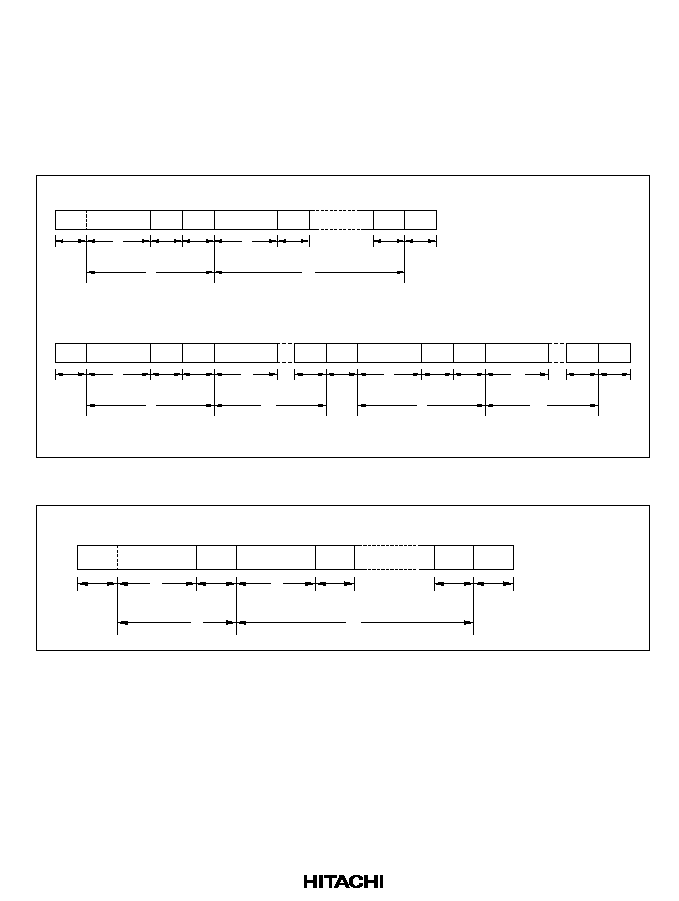
295
13.3
Operation
13.3.1
I
2
C Bus Data Format
The I
2
C bus interface has three data formats: two addressing formats, shown as (a) and (b) in
figure 13.3, and a non-addressing format, shown as (c) in figure 13.4. The first byte following a
start condition always consists of 8 bits. Figure 13.5 shows the I
2
C bus timing.
S
SLA
R/
W
A
DATA
A
A/
A
P
1
1
1
1
n
7
1
m
(a) Addressing format (FS = 0)
(b) Addressing format (retransmit start condition, FS = 0)
n: bit count
(n = 1 to 8)
m: frame count
(m
1)
S
SLA
R/
W
A
DATA
1
1
1
n1
7
1
m1
S
SLA
R/
W
A
DATA
A/
A
P
1
1
1
n2
7
1
m2
1
1
1
A/
A
n1 and n2: bit count (n1 and n2 = 1 to 8)
m1 and m2: frame count (m1 and m2
1)
1
1
Figure 13.3 I
2
C Bus Data Formats (Acknowledge Formats)
S
DATA
A
DATA
A
A/
A
P
1
1
1
n
8
1
m
(c) Non-addressing format (FS = 1)
n: bit count
(n = 1 to 8)
m: frame count
(m
1)
1
1
Figure 13.4 I
2
C Bus Data Format (Non-Acknowledge Format)
Legend:
S:
Start condition. The master device drives SDA from high to low while SCL is high.
SLA:
Slave address, by which the master device selects a slave device.
R/
W:
Indicates the direction of data transfer: from the slave device to the master device when
R/
W is 1, or from the master device to the slave device when R/W is 0.
A:
Acknowledge. The receiving device (the slave in master transmit mode, or the master in
master receive mode) drives SDA low to acknowledge a transfer. If transfers need not be
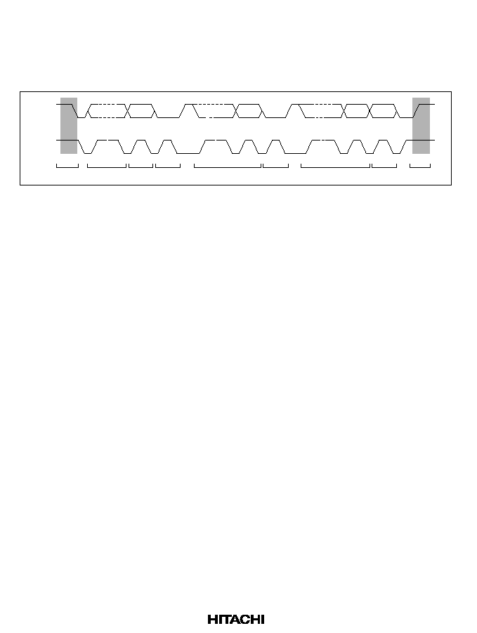
296
acknowledged, set the ACK bit to 1 in ICCR to keep the interface from generating the
acknowledge signal and its clock pulse.
DATA:
Transferred data. The bit length is set by bits BC2 to BC0 in ICMR. The MSB-first or
LSB-first format is selected by bit MLS in ICMR.
P:
Stop condition. The master device drives SDA from low to high while SCL is high.
SDA
SCL
S
1-7
SLA
8
R/W
9
A
1-7
DATA
8
9
1-7
8
9
A
DATA
P
A/
A
Figure 13.5 I
2
C Bus Timing
13.3.2
Master Transmit Operation
In master transmit mode, the master device outputs the transmit clock and transmit data, and the
slave device returns an acknowledge signal. The transmit procedure and operations in master
transmit mode are described below.
1. Set bits MLS and WAIT in ICMR and bits ACK and CKS2 to CKS0 in ICCR according to the
operating mode. Set bit ICE in ICCR to 1.
2. Read BBSY in ICSR, check that the bus is free, then set MST and TRS to 1 in ICCR to select
master transmit mode. After that, write 1 in BBSY and 0 in SCP. This generates a start
condition by causing a high-to-low transition of SDA while SCL is high.
3. Write data in ICDR. The master device outputs the written data together with a sequence of
transmit clock pulses at the timing shown in figure 13.6. If FS is 0 in SAR, the first byte
following the start condition contains a 7-bit slave address and indicates the transmit/receive
direction. The selected slave device (the device with the matching slave address) drives SDA
low at the ninth transmit clock pulse to acknowledge the data.
4. When 1 byte of data has been transmitted, IRIC is set to 1 in ICSR at the rise of the ninth
transmit clock pulse. If IEIC is set to 1 in ICCR, a CPU interrupt is requested. After one frame
has been transferred, SCL is automatically brought to the low level in synchronization with the
internal clock and held low.
5. Software clears IRIC to 0 in ICSR.

297
6. To continue transmitting, write the next transmit data in ICDR. Transmission of the next byte
will begin in synchronization with the internal clock.
Steps 4 to 6 can be repeated to transmit data continuously. To end the transmission, write 0 in
BBSY and 0 in SCP in ICSR. This generates a stop condition by causing a low-to-high transition
of SDA while SCL is high.
1
9
8
7
6
5
4
3
2
1
Bit 7
Bit 6
Bit 5
Bit 4
Bit 3
Bit 2
Bit 1
Bit 0
Bit 7
A
SCL
SDA (master
output)
SDA (slave
output)
IRIC
User
processing
2. Write BBSY = 1
and SCP = 0
Interrupt
request
3. Write to ICDR
5. Clear IRIC
6. Write to ICDR
Figure 13.6 Operation Timing in Master Transmit Mode
(MLS = WAIT = ACK = 0)

298
13.3.3
Master Receive Operation
In master receive mode, the master device outputs the receive clock, receives data, and returns an
acknowledge signal. The slave device transmits the data. The receive procedure and operations in
master receive mode are described below. See also figure 13.7.
1. Clear TRS to 0 in ICCR to switch from transmit mode to receive mode.
2. Read ICDR to start receiving. When ICDR is read, a receive clock is output in synchronization
with the internal clock, and data is received. At the ninth clock pulse the master device drives
SDA low to acknowledge the data.
3. When 1 byte of data has been received, IRIC is set to 1 in ICSR at the rise of the ninth receive
clock pulse. If IEIC is set to 1 in ICCR, a CPU interrupt is requested. After one frame has been
transferred, SCL is automatically brought to the low level in synchronization with the internal
clock and held low.
4. Software clears IRIC to 0 in ICSR.
5. When ICDR is read, receiving of the next data starts in synchronization with the internal clock.
Steps 3 to 5 can be repeated to receive data continuously. To stop receiving, set TRS to 1, read
ICDR, then write write 0 in BBSY and 0 in SCP in ICSR. This generates a stop condition by
causing a low-to-high transition of SDA while SCL is high. If it is not necessary to acknowledge
each bye of data, set ACKB to 1 in ICSR before receiving starts.
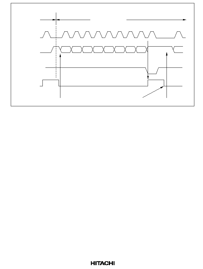
299
9
8
7
6
5
4
3
2
1
1
9
A
A
Bit 0
Bit 1
Bit 2
Bit 3
Bit 4
Bit 5
Bit 6
Bit 7
Interrupt
request
Interrupt
request
Master
transmit
mode
Master receive mode
SCL
SDA (slave
output)
SDA (master
output)
IRIC
User processing
2. Read ICDR
4. Clear IRIC
5. Read ICDR
Figure 13.7 Operation Timing in Master Receive Mode
(MLS = WAIT = ACK = ACKB = 0)

300
13.3.4
Slave Transmit Operation
In slave transmit mode, the slave device outputs the transmit data, and the master device outputs
the transmit clock and returns an acknowledge signal. The transmit procedure and operations in
slave transmit mode are described below.
1. Set bits MLS and WAIT in ICMR and bits MST, TRS, ACK, and CKS2 to CKS0 in ICCR
according to the operating mode. Set bit ICE in ICCR to 1.
2. After the slave device detects a start condition, if the first byte matches its slave address, at the
ninth clock pulse the slave device drives SDA low to acknowledge the transfer. At the same
time, IRIC is set to 1 in ICSR, generating an interrupt. If the eighth data bit (R/
W) is 1, the
TRS bit is set to 1 in ICCR, automatically causing a transition to slave transmit mode. The
slave device holds SCL low from the fall of the transmit clock until data is written in ICDR.
3. Software clears IRIC to 0 in ICSR.
4. Write data in ICDR. The slave device outputs the written data serially in step with the clock
output by the master device, with the timing shown in figure 13.8.
5. When 1 byte of data has been transmitted, at the rise of the ninth transmit clock pulse IRIC is
set to 1 in ICSR. If IEIC is set to 1 in ICCR, a CPU interrupt is requested. The slave device
holds SCL low from the fall of the transmit clock until data is written in ICDR. The master
device drives SDA low at the ninth clock pulse to acknowledge the data. The acknowledge
signal is stored in ACKB in ICSR, and can be used to check whether the transfer was carried
out normally.
6. Software clears IRIC to 0 in ICSR.
7. To continue transmitting, write the next transmit data in ICDR.
Steps 5 to 7 can be repeated to transmit continuously. To end the transmission, write H'FF in
ICDR. When a stop condition is detected (a low-to-high transition of SDA while SCL is high),
BBSY will be cleared to 0 in ICSR.
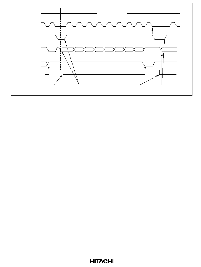
301
Slave receive
mode
Slave transmit mode
SCL (master
output)
SCL (slave
output)
SDA (slave
output)
SDA (master
output)
8
9
1
2
3
4
5
6
7
8
9
1
Bit 7
Bit 6
Bit 5
Bit 4
Bit 3
Bit 2
Bit 1
Bit 0
Bit 7
A
R/W
A
Interrupt
request
Interrupt
request
User processing
3. Clear IRIC
4. Write to ICDR
6. Clear IRIC
7. Write to ICDR
IRIC
Figure 13.8 Operation Timing in Slave Transmit Mode
(MLS = WAIT = ACK = 0)

302
13.3.5
Slave Receive Operation
In slave receive mode, the master device outputs the transmit clock and transmit data, and the
slave device returns an acknowledge signal. The receive procedure and operations in slave receive
mode are described below. See also figure 13.9.
1. Set bits MLS and WAIT in ICMR and bits MST, TRS, and ACK in ICCR according to the
operating mode. Set bit ICE in ICCR to 1, establishing slave receive mode.
2. A start condition output by the master device sets BBSY to 1 in ICSR.
3. After the slave device detects the start condition, if the first byte matches its slave address, at
the ninth clock pulse the slave device drives SDA low to acknowledge the transfer. At the
same time, IRIC is set to 1 in ICSR. If IEIC is 1 in ICCR, a CPU interrupt is requested. The
slave device holds SCL low from the fall of the receive clock until it has read the data in
ICDR.
4. Software clears IRIC to 0 in ICSR.
5. When ICDR is read, receiving of the next data starts.
Steps 4 and 5 can be repeated to receive data continuously. When a stop condition is detected (a
low-to-high transition of SDA while SCL is high), BBSY is cleared to 0 in ICSR.
Start condition
SCL (master
output)
SCL (slave
output)
SDA (master
output
SDA (slave
output)
IRIC
A
Bit 7
Bit 6
Bit 5
Bit 4
Bit 3
Bit 2
Bit 1
Bit 0
Bit 7
Interrupt
request
4. Clear IRIC
5. Read ICDR
User processing
1
9
8
7
6
5
4
3
2
1
Figure 13.9 Operation Timing in Slave Receive Mode
(MLS = WAIT = ACK = ACKB = 0)
303
13.3.6
IRIC Set Timing and SCL Control
The interrupt request flag (IRIC) is set at different times depending on the WAIT bit in ICMR and
ACK bit in ICCR. SCL is automatically held low after one frame has been transferred; this timing
is synchronized with the internal clock. Figure 13.10 shows the IRIC set timing and SCL control.
(a) When WAIT = 0 and ACK = 0
SCL
SDA
IRIC
User processing
Clear IRIC
Write to ICDR (transmit)
or read ICDR (receive)
1
A
8
7
(b) When WAIT = 1 and ACK = 0
SCL
SDA
IRIC
User processing
Clear IRIC
Write to ICDR (transmit)
or read ICDR (receive)
Note: The ICDR write (transmit) or read (receive) following the clearing of IRIC
should be executed after the rise of SCL (ninth clock pulse).
SCL
SDA
IRIC
User processing
(c) When ACK = 1
Clear IRIC
Write to ICDR (transmit)
or read ICDR (receive)
A
8
7
1
8
7
1
Figure 13.10 IRIC Set Timing and SCL Control

304
13.3.7
Noise Canceler
The logic levels at the SCL and SDA pins are routed through noise cancelers before being latched
internally. Figure 13.11 shows a block diagram of the noise canceler.
The noise canceler consists of two cascaded latches and a match detector. The SCL (or SDA)
input signal is sampled on the system clock, but is not passed forward to the next circuit unless the
outputs of both latches agree. If they do not agree, the previous value is held.
t
Sampling clock
C
D
Q
Latch
C
D
Q
Latch
SCL or
SDA input
signal
Match
detector
Internal
SCL or
SDA
signal
Sampling
clock
t: System clock
Figure 13.11 Block Diagram of Noise Canceler
305
13.3.8
Sample Flowcharts
Figures 13.12 to 13.15 show typical flowcharts for using the I
2
C bus interface in each mode.
1
2
3
4
5
6
7
8
9
10
Start
Initialize
Read BBSY in ICSR
No
BBSY = 0?
Yes
Set MST = 1 and
TRS = 1 in ICCR
Write BBSY = 1
and SCP = 0 in ICSR
Write transmit data in ICDR
Read IRIC in ICSR
No
Yes
IRIC = 1?
Clear IRIC in ICSR
Read ACKB in ICSR
ACKB = 0?
No
Yes
No
Yes
Transmit mode?
Write transmit data in ICDR
Read IRIC in ICSR
IRIC = 1?
No
Yes
Clear IRIC in ICSR
Read ACKB in ICSR
End of transmission
(ACKB = 1)?
No
Yes
Write BBSY = 0
and SCP = 0 in ICSR
End
Master receive mode
1.
Test the status of the SCL and SDA lines.
2.
Select master transmit mode.
3.
Generate a start condition.
4.
Set transmit data for the first byte (slave address + R/W).
5.
Wait for 1 byte to be transmitted.
6.
Test for acknowledgement by the designated slave device.
7.
Set transmit data for the second and subsequent bytes.
8.
Wait for 1 byte to be transmitted.
9.
Test for end of transfer.
10. Generate a stop condition.
Figure 13.12 Flowchart for Master Transmit Mode (Example)
306
Master receive mode
Set TRS = 0 in ICCR
Set ACKB = 0 in ICSR
Last receive?
Read ICDR
Read IRIC in ICSR
Clear IRIC in ICSR
IRIC = 1?
Yes
No
No
Yes
Set ACKB = 1 in ICSR
Read ICDR
Read IRIC in ICSR
IRIC = 1?
Clear IRIC in ICSR
Set TRS = 1 in ICCR
Read ICDR
Write BBSY = 0
and SCP = 0 in ICSR
End
1
2
3
4
5
6
7
8
9
10
Yes
No
1. Select receive mode.
2. Set acknowledgement data.
3. Start receiving. The first read is a dummy read.
4. Wait for 1 byte to be received.
5. Set acknowledgement data for the last receive.
6. Start the last receive.
7. Wait for 1 byte to be received.
8. Select transmit mode.
9. Read the last receive data (if ICDR is read
without selecting transmit mode, receive
operations will resume).
10. Generate a stop condition.
Figure 13.13 Flowchart for Master Receive Mode (Example)
307
Slave transmit mode
Write transmit data in ICDR
Read IRIC in ICSR
IRIC = 1?
Clear IRIC in ICSR
Read ACKB in ICSR
Write TRS = 0 in ICCR
End
of transmission
(ACKB = 1)?
Yes
No
No
Yes
End
1
2
3
Read ICDR
5
4
1. Set transmit data for the second and
subsequent bytes.
2. Wait for 1 byte to be transmitted.
3. Test for end of transfer.
4. Select slave receive mode.
5. Dummy read (to release the SCL line).
Figure 13.14 Flowchart for Slave Transmit Mode (Example)
308
Start
Initialize
Set MST = 0
and TRS = 0 in ICCR
Write ACKB = 0 in ICSR
Read IRIC in ICSR
IRIC = 1?
Yes
No
Clear IRIC in ICSR
Read AAS and ADZ in ICSR
AAS = 1
and ADZ = 0?
Read TRS in ICCR
TRS = 0?
No
Yes
No
Yes
Yes
No
Yes
Yes
No
No
1
2
3
4
5
6
7
8
Last receive?
Read ICDR
Read IRIC in ICSR
IRIC = 1?
Clear IRIC in ICSR
Set ACKB = 1 in ICSR
Read ICDR
Read IRIC in ICSR
Clear IRIC in ICSR
IRIC = 1?
Read ICDR
End
General call address processing
*
Description omitted
Slave transmit mode
1.
Select slave receive mode.
2.
Wait for the first byte to be received.
3.
Start receiving. The first read is a dummy read.
4.
Wait for the transfer to end.
5.
Set acknowledgement data for the last receive.
6.
Start the last receive.
7.
Wait for the transfer to end.
8.
Read the last receive data.
Figure 13.15 Flowchart for Slave Receive Mode (Example)

309
13.4
Application Notes
1. In master mode, if an instruction to generate a start condition is immediately followed by an
instruction to generate a stop condition, neither condition will be output correctly. To output
consecutive start and stop conditions, after issuing the instruction that generates the start
condition, read the relevant ports, check that SCL and SDA are both low, then issue the
instruction that generates the stop condition.
2. Either of the following two conditions will start the next transfer. Pay attention to these
conditions when reading or writing to ICDR.
Write access to ICDR when ICE = 1 and TRS = 1
Read access to ICDR when ICE = 1 and TRS = 0
3. The I
2
C bus interface specification for the SCL rise time tsr is under 1000 ns (300 ns for high-
speed mode). In master mode, the I
2
C bus interface monitors the SCL line and synchronizes
one bit at a time during communication. If tsr (the time for SCL to go from low to V
IH
) exceeds
the time determined by the input clock of the I
2
C bus interface, the high period of SCL is
extended. SCL rise time is determined by the pull-up resistance and load capacitance of the
SCL line. To insure proper operation at the set transfer rate, adjust the pull-up resistance and
load capacitance so that the SCL rise time falls below the values given in the table below.
t
cyc
Time Display
CKDBL
IICX
Display
¯ = 5 MHz
¯ = 8 MHz
¯ = 10 MHz ¯ = 16 MHz
0
0
7.5t
cyc
Normal
mode
1000 ns
937 ns
750 ns
486 ns
High-speed
mode
300 ns
300 ns
300 ns
300 ns
0
1
17.5t
cyc
Normal
mode
1000 ns
1000 ns
1000 ns
1000 ns
1
0
High-speed
mode
300 ns
300 ns
300 ns
300 ns
1
1
37.5t
cyc
Normal
mode
1000 ns
1000 ns
1000 ns
1000 ns
High-speed
mode
300 ns
300 ns
300 ns
300 ns
4. Note on Issuance of Retransmission Start Condition
When issuing a retransmission start condition, the condition must be issued after the SCL clock
falls during the acknowledge bit reception period. After the end of the acknowledge bit, the
next data should be written to ICDR after SCL goes high. Figure 13.16 shows the
recommended program flow for issuing a retransmission start condition. A timing chart for the
flowchart in figure 13.16 is shown in figure 13.17.

310
IRIC = 1?
Read IRIC in ICSR
Clear IRIC in ICSR
Retransmission?
Read SCL
SCL = 0?
Write 1 to BBSY and
0 to SCP in ICSR
Read SCL
Write data to ICDR
Other operation
No
No
Yes
Yes
SCL = 1?
No
Yes
(1) Confirm completion of 1-
byte transmission
(2) Confirm that SCL is low
(3) Issue retransmission
start condition
(4) Confirm that SCL is high
(5) Write transmit data
Note: "Read SCL" means
reading DR for the
SCL pin.
Figure 13.16 Recommended Program Flow for Retransmission Start Condition Issuance
SCL
SDA
IRIC
(1) IRIC check
(2) SCL low level
determination
(4) SCL high level
determination
(5) Transmit data setting
(3) Retransmission start
condition issuance
9
ACK
Bit 7
Figure 13.17 Timing Chart for Retransmission Start Condition Issuance

311
5. Note on Issuance of Stop Condition
If the rise of SCL is weakened by external pull-up resistance R and bus load capacitance C in
master mode, or if SCL is pulled to the low level by a slave device, the timing at which SCL is
lowered by the internal bit synchronization circuit may be delayed by 1t SCL. If, in this case,
SCL is identified as being low at the bit synchronization circuit sampling timing, and a stop
condition issuing instruction is executed before the reference SCL clock next falls, as in figure
13.18, SDA will change from high to low to high while SCL remains high. As a result, a stop
condition will be issued before the end of the 9th clock.
9
9
Bit synchronization circuit sampling timing
V
IH
V
IH
Normal operation
Erroneous
operation
SCL output
SDA output
SCL output
SDA output
Normal
operation
Erroneous
operation
Reference clock
SCL
SDA
IRIC
Bus line
Stop condition issuing instruction
execution timing
9th clock not ended
Stop condition
Stop condition
High interval secured
SCL identified as low
Figure 13.18 Stop Condition Erroneous Operation Timing
312
6. Countermeasure
Figure 13.19 shows the recommended program flow.
IRIC = 1?
Read IRIC in ICSR
Read ACKB in ICSR
ACKB = 1?
Read SCL
SCL = 0?
Write 0 to BBSY and
0 to SCP in ICSR
Transmit
data present?
Write data to ICDR
Yes
Yes
No
No
Yes
No
Yes
No
Figure 13.19 Recommended Program Flow
7. Additional Note
When switching from master receive mode to master transmit mode, ensure that TRS is set to 1
before the last receive data is latched by reading ICDR.
8. Precautions when Clearing the IRIC Flag when Using the Wait Function
If the SCL rise time exceeds the specified duration when using the wait function in the I
2
C bus
interface's master mode, or if there is a slave device that keeps SCL low and applies a wait
state, read SCL and clear the IRIC flag only after determining that SCL has gone low, as
shown below.
If the IRIC flag is cleared to 0 when WAIT is set to 1 and while the SCL high level duration is
being extended, the SDA value may change before SCL falls, erroneously resulting in a start or
stop condition.

313
SCL
VIH
SDA
IRIC
IRIC cleared
SCL determined to be low level
SCL low level detected
SCL high level duration maintained
Figure 13.20 IRIC Flag Clear Timing when WAIT = 1
Note that the clock may not be output properly during the next master send if receive data
(ICDR data) is read during the time between when the instruction to issue a stop condition is
executed (writing 0 to BBSY and SCP in ISSR) and when the stop condition is actually
generated.
In addition, overwriting of IIC control bits in order to change the send or receive operation
mode or to change settings, such as for example clearing the MST bit after completion of
master send or receive, should always be performed during the period indicated as (a) in Figure
13.21 below (after confirming that the BBSY bit in the ICCR register has been cleared to 0).
Master receive mode
ICDR read F
prohibited duration
BBSY bit
Internal clock
SCL
SDA
A
8
9
(a)
Bit 0
Stop condition
Start condition
Execution of issue
stop condition instruction
(BBSY = 0 and SCP = 0 written)
Stop condition generated
(BBSY = 0 read)
Start condition issued
Figure 13.21 Precautions when Reading Master Receive Data

314

315
Section 14 Host Interface (H8/3337 Series Only)
14.1
Overview
The H8/3337 Series has an on-chip host interface (HIF) that provides a dual-channel parallel
interface between the on-chip CPU and a host processor. The host interface is available only when
the HIE bit is set to 1 in SYSCR. This mode is called slave mode, because it is designed for a
master-slave communication system in which the H8/3337-Series chip is slaved to a host
processor.
The host interface consists of four 1-byte data registers, two 1-byte status registers, a 1-byte
control register, fast A
20
gate logic, and a host interrupt request circuit. Communication is carried
out via five control signals from the host processor (
CS
1
,
CS
2
or
ECS
2
, HA
0
,
IOR, and IOW or
EIOW), four output signals to the host processor (GA
20
, HIRQ
1
, HIRQ
11
, and HIRQ
12
), and an 8-
bit bidirectional command/data bus (HDB
7
to HDB
0
). The
CS
1
and
CS
2
(or
ECS
2
) signals select
one of the two interface channels.
Note:
If one of the two interface channels will not be used, tie the unused
CS pin to V
CC
. For
example, if interface channel 1 (IDR1, ODR1, STR1) is not used, tie
CS
1
to V
CC
.
316
14.1.1
Block Diagram
Figure 14.1 is a block diagram of the host interface.
(Internal interrupt signals)
IBF2
IBF1
Control
logic
HDB
7
≠HDB
0
IDR1
ODR1
STR1
IDR2
ODR2
STR2
HICR
Module data bus
Host data bus
Host
interrupt
request
Fast
A
20
gate
control
Port 4
Port 8
Internal data bus
Bus
interface
CS
1
ECS
2
/CS
2
IOR
EIOW
/
IOW
HA
0
HIRQ
1
HIRQ
11
HIRQ
12
GA
20
Legend:
IDR1:
IDR2:
ODR1:
ODR2:
STR1:
STR2:
HICR:
Input data register 1
Input data register 2
Output data register 1
Output data register 2
Status register 1
Status register 2
Host interface control register
Figure 14.1 Host Interface Block Diagram

317
14.1.2
Input and Output Pins
Table 14.1 lists the input and output pins of the host interface module.
Table 14.1
HIF Input/Output Pins
Name
Abbreviation
Port
I/O
Function
I/O read
IOR
P8
3
Input
Host interface read signal
I/O write
*
IOW
P8
4
Input
Host interface write signal
EIOW
P9
1
Chip select 1
CS
1
P8
2
Input
Host interface chip select signal for
IDR1, ODR1, STR1
Chip select 2
*
CS
2
P8
5
Input
Host interface chip select signal for
ECS
2
P9
0
IDR2, ODR2, STR2
Command/data
HA
0
P8
0
Input
Host interface address select signal
In host read access, this signal
selects the status registers (STR1,
STR2) or data registers (ODR1,
ODR2). In host write access to the
data registers (IDR1, IDR2), this
signal indicates whether the host is
writing a command or data.
Data bus
HDB
7
≠HDB
0
P3
7
≠P3
0
I/OHost interface data bus (single-chip
mode)
Host interrupt 1
HIRQ
1
P4
4
Output
Host interrupt output 1 to host
Host interrupt 11
HIRQ
11
P4
3
Output
Host interrupt output 11 to host
Host interrupt 12
HIRQ
12
P4
5
Output
Host interrupt output 12 to host
Gate A
20
GA
20
P8
1
Output
A
20
gate control signal output
Note:
*
Selection between
IOW
and
EIOW
, and between
CS
2
and
ECS
2
, is by the STAC bit in
STCR.
IOW
and
CS
2
are used when STAC is 0.
EIOW
and
ECS
2
are used when STAC is 1.
In this manual, both are referred to as
IOW
and
CS
2
.

318
14.1.3
Register Configuration
Table 14.2 lists the host interface registers.
Table 14.2
HIF Registers
R/W
Initial
Slave
Master Address
*
4
Name
Abbreviation
Slave
Host
Value
Address
*
3
CS
1
CS
2
HA
0
System control register SYSCR
R/W
*
1
--
H'09
H'FFC4
--
--
--
Host interface control
register
HICR
R/W
--
H'F8
H'FFF0
--
--
--
Input data register 1
IDR1
R
W
--
H'FFF4
0
1
0/1
*
5
Output data register 1
ODR1
R/W
R
--
H'FFF5
0
1
0
Status register 1
STR1
R/(W)
*
2
R
H'00
H'FFF6
0
1
1
Input data register 2
IDR2
R
W
--
H'FFFC
1
0
0/1
*
5
Output data register 2
ODR2
R/W
R
--
H'FFFD
1
0
0
Status register 2
STR2
R/(W)
*
2
R
H'00
H'FFFE
1
0
1
Serial/timer control
register
STCR
R/W
--
H'00
H'FFC3
--
--
--
Notes:
*
1 Bit 3 is a read-only bit.
*
2 The user-defined bits (bits 7 to 4 and 2) are read/write accessible from the slave
processor.
*
3 Address when accessed from the slave processor.
*
4 Pin inputs used in access from the host processor.
*
5 The HA
0
input discriminates between writing of commands and data.

319
14.2
Register Descriptions
14.2.1
System Control Register (SYSCR)
Bit
7
6
5
4
3
2
1
0
SSBY
STS2
STS1
STS0
XRST
NMIEG
HIE
RAME
Initial value
0
0
0
0
1
0
0
1
Read/Write
R/W
R/W
R/W
R/W
R
R/W
R/W
R/W
SYSCR is an 8-bit read/write register which controls chip operations. Host interface functions are
enabled or disabled by the HIE bit of SYSCR. See section 3.2, System Control Register (SYSCR),
for information on other SYSCR bits. SYSCR is initialized to H'09 by an external reset and in
hardware standby mode.
Bit 1--Host Interface Enable Bit (HIE): Enables or disables the host interface in single-chip
mode. When enabled, the host interface handles host-slave data transfers, operating in slave mode.
Bit 1: HIE
Description
0
The host interface is disabled
(Initial value)
1
The host interface is enabled (slave mode)
14.2.2
Host Interface Control Register (HICR)
Bit
7
6
5
4
3
2
1
0
--
--
--
--
--
IBFIE2
IBFIE1
FGA20E
Initial value
1
1
1
1
1
0
0
0
Slave Read/Write
--
--
--
--
--
R/W
R/W
R/W
Host Read/Write
--
--
--
--
--
--
--
--
HICR is an 8-bit read/write register which controls host interface interrupts and the fast A
20
gate
function. HICR is initialized to H'F8 by a reset and in hardware standby mode.
Bits 7 to 3--Reserved: These bits cannot be modified and are always read as 1.

320
Bit 2--Input Buffer Full Interrupt Enable 2 (IBFIE2): Enables or disables the IBF2 interrupt
to the slave CPU.
Bit 2: IBFIE2
Description
0
IDR2 input buffer full interrupt is disabled
(Initial value)
1
IDR2 input buffer full interrupt is enabled
Bit 1-- Input Buffer Full Interrupt Enable 1 (IBFIE1): Enables or disables the IBF1 interrupt
to the slave CPU.
Bit 1: IBFIE1
Description
0
IDR1 input buffer full interrupt is disabled
(Initial value)
1
IDR1 input buffer full interrupt is enabled
Bit 0--Fast Gate A
20
Enable (FGA20E): Enables or disables the fast A
20
gate function. When the
fast A
20
gate is disabled, a regular-speed A
20
gate signal can be implemented by using software to
manipulate the P8
1
output.
Bit 0: FGA20E
Description
0
Disables fast A
20
gate function
(Initial value)
1
Enables fast A
20
gate function
14.2.3
Input Data Register 1 (IDR1)
Bit
7
6
5
4
3
2
1
0
IDR7
IDR6
IDR5
IDR4
IDR3
IDR2
IDR1
IDR0
Initial value
--
--
--
--
--
--
--
--
Slave Read/Write
R
R
R
R
R
R
R
R
Host Read/Write
W
W
W
W
W
W
W
W
IDR1 is an 8-bit read-only register to the slave processor, and an 8-bit write-only register to the
host processor. When
CS
1
is low, information on the host data bus is written into IDR1 at the
rising edge of
IOW. The HA
0
state is also latched into the C/
D bit in STR1 to indicate whether the
written information is a command or data.
The initial values of IDR1 after a reset or standby are undetermined.

321
14.2.4
Output Data Register 1 (ODR1)
Bit
7
6
5
4
3
2
1
0
ODR7
ODR6
ODR5
ODR4
ODR3
ODR2
ODR1
ODR0
Initial value
--
--
--
--
--
--
--
--
Slave Read/Write
R/W
R/W
R/W
R/W
R/W
R/W
R/W
R/W
Host Read/Write
R
R
R
R
R
R
R
R
ODR1 is an 8-bit read/write register to the slave processor, and an 8-bit read-only register to the
host processor. The ODR1 contents are output on the host data bus when HA
0
is low,
CS
1
is low,
and
IOR
is low.
The initial values of ODR1 after a reset or standby are undetermined.
14.2.5
Status Register 1 (STR1)
Bit
7
6
5
4
3
2
1
0
DBU
DBU
DBU
DBU
C/
D
DBU
IBF
OBF
Initial value
0
0
0
0
0
0
0
0
Slave Read/Write
R/W
R/W
R/W
R/W
R
R/W
R
R
Host Read/Write
R
R
R
R
R
R
R
R
STR1 is an 8-bit register that indicates status information during host interface processing. Bits 3,
1, and 0 are read-only bits to both the host and slave processors.
STR1 is initialized to H'00 by a reset and in hardware standby mode.
Bits 7 to 4 and Bit 2--Defined by User (DBU): The user can use these bits as necessary.
Bit 3--Command/Data (C/
D): Receives the HA
0
input when the host processor writes to IDR1,
and indicates whether IDR1 contains data or a command.
Bit 3: C/
D
Description
0
Contents of IDR1 are data
(Initial value)
1
Contents of IDR1 are a command

322
Bit 1--Input Buffer Full (IBF): Set to 1 when the host processor writes to IDR1. This bit is an
internal interrupt source to the slave processor. IBF is cleared to 0 when the slave processor reads
IDR1.
Bit 1: IBF
Description
0
This bit is cleared when the slave processor reads IDR1
(Initial value)
1
This bit is set when the host processor writes to IDR1
Bit 0--Output Buffer Full (OBF): Set to 1 when the slave processor writes to ODR1. Cleared to
0 when the host processor reads ODR1.
Bit 0: OBF
Description
0
This bit is cleared when the host processor reads ODR1
(Initial value)
1
This bit is set when the slave processor writes to ODR1
Table 14.3 shows the conditions for setting and clearing the STR1 flags.
Table 14.3
Set/Clear Timing for STR1 Flags
Flag
Setting Condition
Clearing Condition
C/
D
Rising edge of host's write signal (
IOW
)
when HA
0
is high
Rising edge of host's write signal (
IOW
)
when HA
0
is low
IBF
Rising edge of host's write signal (
IOW
)
when writing to IDR1
Falling edge of slave's internal read signal
(
RD
) when reading IDR1
OBF
Falling edge of slave's internal write
signal (
WR
) when writing to ODR1
Rising edge of host's read signal (
IOR
)
when reading ODR1
14.2.6
Input Data Register 2 (IDR2)
Bit
7
6
5
4
3
2
1
0
IDR7
IDR6
IDR5
IDR4
IDR3
IDR2
IDR1
IDR0
Initial value
--
--
--
--
--
--
--
--
Slave Read/Write
R
R
R
R
R
R
R
R
Host Read/Write
W
W
W
W
W
W
W
W
IDR2 is an 8-bit read-only register to the slave processor, and an 8-bit write-only register to the
host processor. When
CS
2
is low, information on the host data bus is written into IDR2 at the
rising edge of
IOW. The HA
0
state is also latched into the C/
D bit in STR2 to indicate whether the
written information is a command or data.
The initial values of IDR2 after a reset or standby are undetermined.
323
14.2.7
Output Data Register 2 (ODR2)
Bit
7
6
5
4
3
2
1
0
ODR7
ODR6
ODR5
ODR4
ODR3
ODR2
ODR1
ODR0
Initial value
--
--
--
--
--
--
--
--
Slave Read/Write
R/W
R/W
R/W
R/W
R/W
R/W
R/W
R/W
Host Read/Write
R
R
R
R
R
R
R
R
ODR2 is an 8-bit read/write register to the slave processor, and an 8-bit read-only register to the
host processor. The ODR2 contents are output on the host data bus when HA
0
is low,
CS
2
is low,
and
IOR is low.
The initial values of ODR2 after a reset or standby are undetermined.
14.2.8
Status Register 2 (STR2)
Bit
7
6
5
4
3
2
1
0
DBU
DBU
DBU
DBU
C/
D
DBU
IBF
OBF
Initial value
0
0
0
0
0
0
0
0
Slave Read/Write
R/W
R/W
R/W
R/W
R
R/W
R
R
Host Read/Write
R
R
R
R
R
R
R
R
STR2 is an 8-bit register that indicates status information during host interface processing. Bits 3,
1, and 0 are read-only bits to both the host and slave processors.
STR2 is initialized to H'00 by a reset and in hardware standby mode.
Bits 7 to 4 and Bit 2--Defined by User (DBU): The user can use these bits as necessary.
Bit 3--Command/Data (C/
D): Receives the HA
0
input when the host processor writes to IDR2,
and indicates whether IDR2 contains data or a command.
Bit 3: C/
D
Description
0
Contents of IDR2 are data
(Initial value)
1
Contents of IDR2 are a command

324
Bit 1--Input Buffer Full (IBF): Set to 1 when the host processor writes to IDR2. This bit is an
internal interrupt source to the slave processor. IBF is cleared to 0 when the slave processor reads
IDR2.
Bit 1: IBF
Description
0
This bit is cleared when the slave processor reads IDR2
(Initial value)
1
This bit is set when the host processor writes to IDR2
Bit 0--Output Buffer Full (OBF): Set to 1 when the slave processor writes to ODR2. Cleared to
0 when the host processor reads ODR2.
Bit 0: OBF
Description
0
This bit is cleared when the host processor reads ODR2
(Initial value)
1
This bit is set when the slave processor writes to ODR2
Table 14.4 shows the conditions for setting and clearing the STR2 flags.
Table 14.4
Set/Clear Timing for STR2 Flags
Flag
Setting Condition
Clearing Condition
C/
D
Rising edge of host's write signal (
IOW
)
when HA
0
is high
Rising edge of host's write signal (
IOW
)
when HA
0
is low
IBF
Rising edge of host's write signal (
IOW
)
when writing to IDR2
Falling edge of slave's internal read signal
(
RD
) when reading IDR2
OBF
Falling edge of slave's internal write
signal (
WR
) when writing to ODR2
Rising edge of host's read signal (
IOR
)
when reading ODR2

325
14.2.9
Serial/Timer Control Register (STCR)
Bit
7
6
5
4
3
2
1
0
IICS
IICD
IICX
IICE
STAC
MPE
ICKS1
ICKS0
Initial value
0
0
0
0
0
0
0
0
Read/Write
R/W
R/W
R/W
R/W
R/W
R/W
R/W
R/W
STCR is an 8-bit readable/writable register that controls the I
2
C bus interface and host interface
and the SCI operating mode, and selects the TCNT clock source. STCR is initialized to H'00 by a
reset and in hardware standby mode.
Bits 7 to 4--I
2
C Control (IICS, IICD, IICX, IICE): These bits are used to control the I
2
C bus
interface. For details, see section 13, I
2
C Bus Interface.
Bit 3--Slave Input Switch (STAC): Controls switching of host interface input pins. Settings of
this bit are valid only when the host interface is enabled (slave mode).
Bit 3: STAC
Description
0
In port 8, P8
5
switches over to
CS
2
, and P8
4
to
IOW
(Initial value)
1
In port 9, P9
1
switches over to
EIOW
, and P9
0
to
ECS
2
Bit 2--Multiprocessor Enable (MPE): Controls the operating mode of SCI0 and SCI1. For
details, see section 12, Serial Communication Interface.
Bits 1 and 0--Internal Clock Source Select 1 and 0 (ICKS1, ICSK0): Together with bits CKS2
to CKS0 in TCR, these bits select timer counter clock inputs. For details, see section 9, 8-Bit
Timers.

326
14.3
Operation
14.3.1
Host Interface Operation
The host interface is activated by setting the HIE bit (bit 1) to 1 in SYSCR, establishing slave
mode. Activation of the host interface (entry to slave mode) appropriates the related I/O lines in
port 3 or B (data), port 8 or 9 (control) and port 4 (host interrupt requests) for interface use.
For host interface read/write timing diagrams, see section 23.3.8, Host Interface Timing.
14.3.2
Control States
Table 14.5 indicates the slave operations carried out in response to host interface signals from the
host processor.
Table 14.5
Host Interface Operation
CS
2
CS
1
IOR
IOW
HA
0
Slave Operation
1
0
0
0
0
Prohibited
1
Prohibited
1
0
Data read from output data register 1 (ODR1)
1
Status read from status register 1 (STR1)
1
0
0
Data write to input data register 1 (IDR1)
1
Command write to input data register 1 (IDR1)
1
0
Idle state
1
Idle state
0
1
0
0
0
Prohibited
1
Prohibited
1
0
Data read from output data register 2 (ODR2)
1
Status read from status register 2 (STR2)
1
0
0
Data write to input data register 2 (IDR2)
1
Command write to input data register 2 (IDR2)
1
0
Idle state
1
Idle state

327
14.3.3
A
20
Gate
The A
20
gate signal can mask address A
20
to emulate an addressing mode used by personal
computers with an 8086*-family CPU. In slave mode, a regular-speed A
20
gate signal can be
output under software control, or a fast A
20
gate signal can be output under hardware control. Fast
A
20
gate output is enabled by setting the FGA20E bit (bit 0) to 1 in HICR (H'FFF0).
Note: * Intel microprocessor.
Regular A
20
Gate Operation: Output of the A
20
gate signal can be controlled by an H'D1
command followed by data. When the slave processor receives data, it normally uses an interrupt
routine activated by the IBF1 interrupt to read IDR1. If the data follows an H'D1 command,
software copies bit 1 of the data and outputs it at the gate A
20
pin (P8
1
/GA
20
).
Fast A
20
Gate Operation: When the FGA20E bit is set to 1, P8
1
/GA
20
is used for output of a fast
A
20
gate signal. Bit P8
1
DDR must be set to 1 to assign this pin for output. The initial output from
this pin will be a logic 1, which is the initial DR value. Afterward, the host processor can
manipulate the output from this pin by sending commands and data. This function is available
only when register IDR1 is accessed using
CS
1
. Slave logic decodes the commands input from the
host processor. When an H'D1 host command is detected, bit 1 of the data following the host
command is output from the GA
20
output pin. This operation does not depend on software or
interrupts, and is faster than the regular processing using interrupts. Table 14.6 lists the conditions
that set and clear GA
20
(P8
1
). Figure 14.2 describes the GA
20
output in flowchart form. Table 14.7
indicates the GA
20
output signal values.
Table 14.6
GA
20
(P8
1
) Set/Clear Timing
Pin Name
Setting Condition
Clearing Condition
GA20 (P8
1
)
Rising edge of the host's write signal
(
IOW
) when bit 1 of the written data
is 1 and the data follows an H'D1
host command
Rising edge of the host's write signal
(
IOW
) when bit 1 of the written data is 0
and the data follows an H'D1 host
command
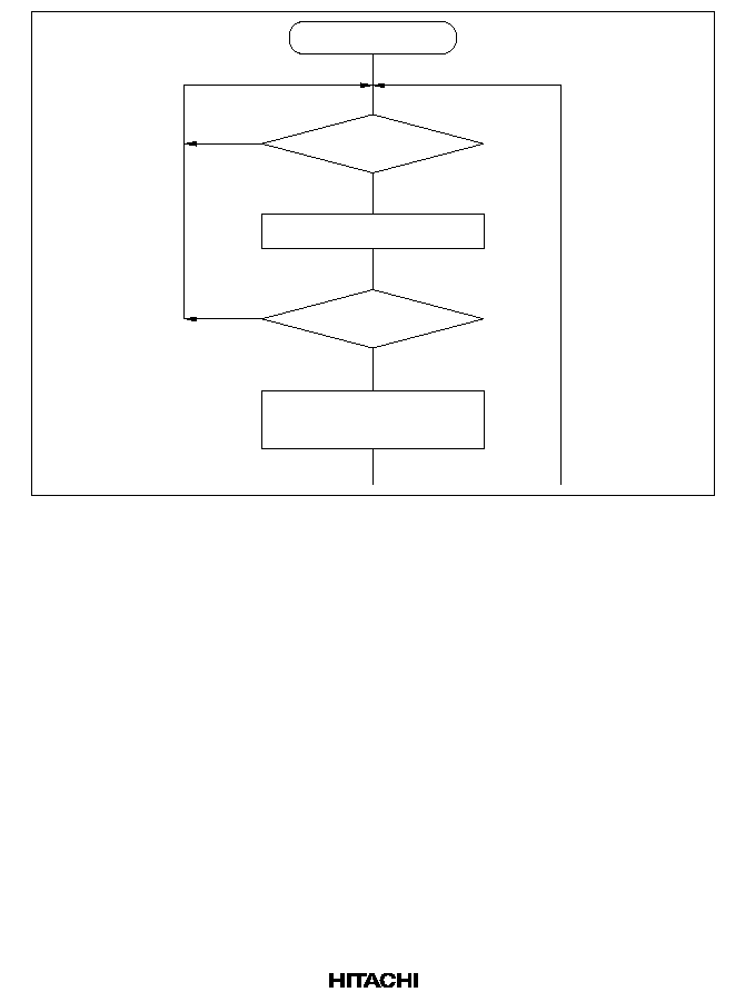
328
Start
Host write
H'D1 command
received?
Wait for next byte
Host write
Yes
Data byte?
Write bit 1 of data byte
to DR bit of P8
1
/GA
20
Yes
No
No
Figure 14.2 GA
20
Output

329
Table 14.7
Fast A
20
Gate Output Signal
HA
0
Data/Command
Internal CPU
Interrupt Flag
GA
20
(PB
1
)
Remarks
1
D1 command
0
Q
Turn-on sequence
0
1 data
*
1
0
1
1
FF command
0
Q (1)
1
D1 command
0
Q
Turn-off sequence
0
0 data
*
2
0
0
1
FF command
0
Q (0)
1
D1 command
0
Q
Short turn-on sequence
0
1 data
*
1
0
1
1/0
Command other than FF
and D1
1
Q (1)
1
D1 command
0
Q
Short turn-off sequence
0
0 data
*
2
0
0
1/0
Command other than FF
and D1
1
Q (0)
1
D1 command
0
Q
Cancelled sequence
1
Command other than D1
1
Q
1
D1 command
0
Q
Retriggered sequence
1
D1 command
0
Q
1
D1 command
0
Q
Consecutively executed
0
Any data
0
1/0
sequences
1
D1 command
0
Q (1/0)
Notes:
*
1 Arbitrary data with bit 1 set to 1.
*
2 Arbitrary data with bit 1 cleared to 0.

330
14.4
Interrupts
14.4.1
IBF1, IBF2
The host interface can request two types of interrupts to the slave CPU: IBF1 and IBF2. They are
input buffer full interrupts for input data registers IDR1 and IDR2 respectively. Each interrupt is
enabled when the corresponding enable bit is set (table 14.8).
Table 14.8
Input Buffer Full Interrupts
Interrupt
Description
IBF1
Requested when IBFIE1 is set to 1 and IDR1 is full
IBF2
Requested when IBFIE2 is set to 1 and IDR2 is full
14.4.2
HIRQ
11
, HIRQ
1
, and HIRQ
12
In slave mode (when HIE = 1 in SYSCR in single-chip mode), three bits in the port 4 data register
(P4DR) can be used as host interrupt request latches.
These three P4DR bits are cleared to 0 by the host processor's read signal (
IOR). If CS
1
and HA
0
are low, when
IOR goes low and the host reads ODR1, HIRQ
1
and HIRQ
12
are cleared to 0. If
CS
2
and HA
0
are low, when
IOR goes low and the host reads ODR2, HIRQ
11
is cleared to 0. To
generate a host interrupt request, normally on-chip software writes 1 to the corresponding bit. In
processing the interrupt, the host's interrupt-handling routine reads the output data register (ODR1
or ODR2), and this clears the host interrupt latch to 0.
Table 14.9 indicates how these bits are set and cleared. Figure 14.3 shows the processing in
flowchart form.
Table 14.9
Host Interrupt Signal Set/Clear Conditions
Host Interrupt
Signal
Setting Condition
Clearing Condition
HIRQ
11
(P4
3
)
Slave CPU reads 0 from P4DR bit 3,
then writes 1
Slave CPU writes 0 in P4DR bit 3, or
host reads output data register 2
HIRQ
1
(P4
4
)
Slave CPU reads 0 from P4DR bit 4,
then writes 1
Slave CPU writes 0 in P4DR bit 4, or
host reads output data register 1
HIRQ
12
(P4
5
)
Slave CPU reads 0 from P4DR bit 5,
then writes 1
Slave CPU writes 0 in P4DR bit 5, or
host reads output data register 1
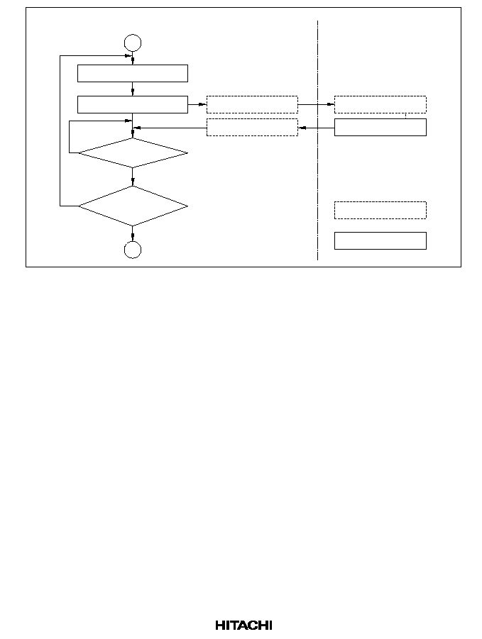
331
Slave CPU
Master CPU
Write to ODR
Write 1 to P4DR
P4DR = 0?
Yes
No
No
Yes
All bytes
transferred?
HIRQ output high
HIRQ output low
Interrupt initiation
ODR read
Hardware operations
Software operations
Figure 14.3 HIRQ Output Flowchart
14.5
Application Note
The host interface provides buffering of asynchronous data from the host and slave processors, but
an interface protocol must be followed to implement necessary functions and avoid data
contention. For example, if the host and slave processors try to access the same input or output
data register simultaneously, the data will be corrupted. Interrupts can be used to design a simple
and effective protocol.

332

333
Section 15 A/D Converter
15.1
Overview
The H8/3337Series and H8/3397 Series include a 10-bit successive-approximations A/D converter
with a selection of up to eight analog input channels.
15.1.1
Features
A/D converter features are listed below.
∑
10-bit resolution
∑
Eight input channels
∑
High-speed conversion
Conversion time: minimum 8.4 µs per channel (with 16-MHz system clock)
∑
Two conversion modes
Single mode: A/D conversion of one channel
Scan mode: continuous conversion on one to four channels
∑
Four 16-bit data registers
A/D conversion results are transferred for storage into data registers corresponding to the
channels.
∑
Sample-and-hold function
∑
A/D conversion can be externally triggered
∑
A/D interrupt requested at end of conversion
At the end of A/D conversion, an A/D end interrupt (ADI) can be requested.
334
15.1.2
Block Diagram
Figure 15.1 shows a block diagram of the A/D converter.
Module data bus
Bus interface
Internal
data bus
ADDRA
ADDRB
ADDRC
ADDRD
ADCSR
ADCR
Successive-
approximations register
10-bit D/A
AV
CC
Analog
multi-
plexer
AN
AN
AN
AN
AN
AN
AN
AN
0
1
2
3
4
5
6
7
Sample-and-
hold circuit
Comparator
+
≠
Control circuit
ADTRG
¯p/8
¯p/16
ADI
interrupt
signal
Legend:
ADCR:
ADCSR:
ADDRA:
ADDRB:
ADDRC:
ADDRD:
A/D control register
A/D control/status register
A/D data register A
A/D data register B
A/D data register C
A/D data register D
AV
SS
Figure 15.1 A/D Converter Block Diagram

335
15.1.3
Input Pins
Table 15.1 lists the A/D converter's input pins. The eight analog input pins are divided into two
groups: group 0 (AN
0
to AN
3
), and group 1 (AN
4
to AN
7
). AV
CC
and AV
SS
are the power supply
for the analog circuits in the A/D converter.
Table 15.1
A/D Converter Pins
Pin Name
Abbreviation
I/O
Function
Analog power supply pin
AV
CC
Input
Analog power supply
Analog ground pin
AV
SS
Input
Analog ground and reference voltage
Analog input pin 0
AN
0
Input
Group 0 analog inputs
Analog input pin 1AN
1
Input
Analog input pin 2
AN
2
Input
Analog input pin 3
AN
3
Input
Analog input pin 4
AN
4
Input
Group 1 analog inputs
Analog input pin 5
AN
5
Input
Analog input pin 6
AN
6
Input
Analog input pin 7
AN
7
Input
A/D external trigger input pin
ADTRG
Input
External trigger input for starting A/D
conversion

336
15.1.4
Register Configuration
Table 15.2 summarizes the A/D converter's registers.
Table 15.2
A/D Converter Registers
Name
Abbreviation
R/W
Initial Value
Address
A/D data register A (high)
ADDRAH
R
H'00
H'FFE0
A/D data register A (low)
ADDRAL
R
H'00
H'FFE1
A/D data register B (high)
ADDRBH
R
H'00
H'FFE2
A/D data register B (low)
ADDRBL
R
H'00
H'FFE3
A/D data register C (high)
ADDRCH
R
H'00
H'FFE4
A/D data register C (low)
ADDRCL
R
H'00
H'FFE5
A/D data register D (high)
ADDRDH
R
H'00
H'FFE6
A/D data register D (low)
ADDRDL
R
H'00
H'FFE7
A/D control/status register
ADCSR
R/W
*
H'00
H'FFE8
A/D control register
ADCR
R/W
H'7F
H'FFE9
Note:
*
Only 0 can be written in bit 7, to clear the flag.

337
15.2
Register Descriptions
15.2.1
A/D Data Registers A to D (ADDRA to ADDRD)
Bit
1
5
1
4
1
3
1
2
1
1
1
0
9
8
7
6
5
4
3
2
1
0
ADDRn
AD9 AD8 AD6 AD5 AD4 AD3 AD2 AD1AD0
--
--
--
--
--
--
--
Initial value
0
0
0
0
0
0
0
0
0
0
0
0
0
0
0
0
Read/Write
R
R
R
R
R
R
R
R
R
R
R
R
R
R
R
R
(N = A to D)
The four A/D data registers (ADDRA to ADDRD) are 16-bit read-only registers that store the
results of A/D conversion.
An A/D conversion produces 10-bit data, which is transferred for storage into the A/D data
register corresponding to the selected channel. The upper 8 bits of the result are stored in the upper
byte of the A/D data register. The lower 2 bits are stored in the lower byte. Bits 5 to 0 of an A/D
data register are reserved bits that always read 0. Table 15.3 indicates the pairings of analog input
channels and A/D data registers.
The CPU can always read and write the A/D data registers. The upper byte can be read directly,
but the lower byte is read through a temporary register (TEMP). For details see section 15.3, CPU
Interface.
The A/D data registers are initialized to H'0000 by a reset and in standby mode.
Table 15.3
Analog Input Channels and A/D Data Registers
Analog Input Channel
Group 0Group 1
A/D Data Register
AN
0
AN
4
ADDRA
AN
1
AN
5
ADDRB
AN
2
AN
6
ADDRC
AN
3
AN
7
ADDRD

338
15.2.2
A/D Control/Status Register (ADCSR)
Bit
7
6
5
4
3
2
1
0
ADF
ADIE
ADST
SCAN
CKS
CH2
CH1CH0
Initial value
0
0
0
0
0
0
0
0
Read/Write
R/(W)
*
R/W
R/W
R/W
R/W
R/W
R/W
R/W
Note:
*
Only 0 can be written, to clear the flag.
ADCSR is an 8-bit readable/writable register that selects the mode and controls the A/D converter.
ADCSR is initialized to H'00 by a reset and in standby mode.
Bit 7--A/D End Flag (ADF): Indicates the end of A/D conversion.
Bit 7: ADF
Description
0
Clearing condition:
(Initial value)
Cleared by reading ADF while ADF = 1, then writing 0 in ADF
1Setting conditions:
∑
Single mode: A/D conversion ends
∑
Scan mode: A/D conversion ends in all selected channels
Bit 6--A/D Interrupt Enable (ADIE): Enables or disables the interrupt (ADI) requested at the
end of A/D conversion.
Bit 6: ADIE
Description
0
A/D end interrupt request (ADI) is disabled
(Initial value)
1A/D end interrupt request (ADI) is enabled
Bit 5--A/D Start (ADST): Starts or stops A/D conversion. The ADST bit remains set to 1 during
A/D conversion. It can also be set to 1 by external trigger input at the
ADTRG pin.
Bit 5: ADST
Description
0
A/D conversion is stopped
(Initial value)
1
∑
Single mode: A/D conversion starts; ADST is automatically cleared to 0
when conversion ends
∑
Scan mode: A/D conversion starts and continues, cycling among the
selected channels, until ADST is cleared to 0 by software, by a reset, or by
a transition to standby mode

339
Bit 4--Scan Mode (SCAN): Selects single mode or scan mode. For further information on
operation in these modes, see section 15.4, Operation. Clear the ADST bit to 0 before switching
the conversion mode.
Bit 4: SCAN
Description
0
Single mode
(Initial value)
1Scan mode
Bit 3--Clock Select (CKS): Selects the A/D conversion time. When ¯
P
= ¯/2, the conversion time
doubles. Clear the ADST bit to 0 before switching the conversion time.
Bit 3: CKS
Description
0
Conversion time = 266 states (maximum) (when ¯
P
= ¯)
(Initial value)
1Conversion time = 1
34 states (maximum) (when ¯
P
= ¯)
Bits 2 to 0--Channel Select 2 to 0 (CH2 to CH0): These bits and the SCAN bit select the analog
input channels. Clear the ADST bit to 0 before changing the channel selection.
Group Selection
Channel Selection
Description
CH2
CH1
CH0Single Mode
Scan Mode
0
0
0
AN
0
(initial value)
AN
0
1AN
1
AN
0
, AN
1
1
0
AN
2
AN
0
to AN
2
1AN
3
AN
0
to AN
3
1
0
0
AN
4
AN
4
1AN
5
AN
4
, AN
5
1
0
AN
6
AN
4
to AN
6
1AN
7
AN
4
to AN
7

340
15.2.3
A/D Control Register (ADCR)
Bit
7
6
5
4
3
2
1
0
TRGE
--
--
--
--
--
--
--
Initial value
0
11 11 11 1
Read/Write
R/W
--
--
--
--
--
--
--
ADCR is an 8-bit readable/writable register that enables or disables external triggering of A/D
conversion. ADCR is initialized to H'7F by a reset and in standby mode.
Bit 7--Trigger Enable (TRGE): Enables or disables external triggering of A/D conversion.
Bit 7: TRGE
Description
0
A/D conversion cannot be externally triggered
(Initial value)
1A/D conversion is enabled by the external trigger signal (
ADTRG
) (A/D
conversion can also be enabled by software)
Bits 6 to 0--Reserved: These bits cannot be modified, and are always read as 1.
15.3
CPU Interface
ADDRA to ADDRD are 16-bit registers, but they are connected to the CPU by an 8-bit data bus.
Therefore, although the upper byte can be be accessed directly by the CPU, the lower byte is read
through an 8-bit temporary register (TEMP).
An A/D data register is read as follows. When the upper byte is read, the upper-byte value is
transferred directly to the CPU and the lower-byte value is transferred into TEMP. Next, when the
lower byte is read, the TEMP contents are transferred to the CPU.
When reading an A/D data register, always read the upper byte before the lower byte. It is possible
to read only the upper byte, but if only the lower byte is read, incorrect data may be obtained.
Figure 15.2 shows the data flow for access to an A/D data register.

341
Upper-byte read
Bus interface
Module data bus
CPU
(H'AA)
ADDRnH
(H'AA)
ADDRnL
(H'40)
Lower-byte read
Bus interface
Module data bus
CPU
(H'40)
ADDRnH
(H'AA)
ADDRnL
(H'40)
TEMP
(H'40)
TEMP
(H'40)
(n = A to D)
(n = A to D)
Figure 15.2 A/D Data Register Access Operation (Reading H'AA40)

342
15.4
Operation
The A/D converter operates by successive approximations with 10-bit resolution. It has two
operating modes: single mode and scan mode.
15.4.1
Single Mode (SCAN = 0)
Single mode should be selected when only one A/D conversion on one channel is required. A/D
conversion starts when the ADST bit is set to 1 by software, or by external trigger input. The
ADST bit remains set to 1 during A/D conversion and is automatically cleared to 0 when
conversion ends.
When conversion ends the ADF bit is set to 1. If the ADIE bit is also set to 1, an ADI interrupt is
requested at this time. To clear the ADF flag to 0, first read ADCSR, then write 0 in ADF.
When the mode or analog input channel must be switched during analog conversion, to prevent
incorrect operation, first clear the ADST bit to 0 in ADCSR to halt A/D conversion. After making
the necessary changes, set the ADST bit to 1 to start A/D conversion again. The ADST bit can be
set at the same time as the mode or channel is changed.
Typical operations when channel 1 (AN
1
) is selected in single mode are described next. Figure
15.3 shows a timing diagram for this example.
1. Single mode is selected (SCAN = 0), input channel AN
1
is selected (CH2 = CH1 = 0, CH0 =
1), the A/D interrupt is enabled (ADIE = 1), and A/D conversion is started (ADST = 1).
2. When A/D conversion is completed, the result is transferred into ADDRB. At the same time
the ADF flag is set to 1, the ADST bit is cleared to 0, and the A/D converter becomes idle.
3. Since ADF = 1 and ADIE = 1, an ADI interrupt is requested.
4. The A/D interrupt handling routine starts.
5. The routine reads ADCSR, then writes 0 in the ADF flag.
6. The routine reads and processes the conversion result (ADDRB).
7. Execution of the A/D interrupt handling routine ends. After that, if the ADST bit is set to 1,
A/D conversion starts again and steps 2 to 7 are repeated.

343
ADIE
ADST
ADF
State of channel 0
(AN )
Set
Set
Set
Clear
Clear
Idle
Idle
Idle
Idle
A/D conversion
A/D conversion
Idle
Read conversion result
A/D conversion result
Read conversion result
A/D conversion result
(2)
Note: Vertical arrows ( ) indicate instructions executed by software.
0
1
2
3
A/D conversion
starts
*
*
*
*
*
(2)
(1)
(1)
*
ADDRA
ADDRB
ADDRC
ADDRD
State of channel 1
(AN )
State of channel 2
(AN )
State of channel 3
(AN )
Idle
Figure 15.3 Example of A/D Converter Operation (Single Mode, Channel 1 Selected)

344
15.4.2
Scan Mode (SCAN = 1)
Scan mode is useful for monitoring analog inputs in a group of one or more channels. When the
ADST bit is set to 1 by software or external trigger input, A/D conversion starts on the first
channel in the group (AN
0
when CH2 = 0, AN
4
when CH2 = 1). When two or more channels are
selected, after conversion of the first channel ends, conversion of the second channel (AN
1
or
AN
5
) starts immediately. A/D conversion continues cyclically on the selected channels until the
ADST bit is cleared to 0. The conversion results are transferred for storage into the A/D data
registers corresponding to the channels.
When the mode or analog input channel selection must be changed during analog conversion, to
prevent incorrect operation, first clear the ADST bit to 0 in ADCSR to halt A/D conversion. After
making the necessary changes, set the ADST bit to 1. A/D conversion will start again from the
first channel in the group. The ADST bit can be set at the same time as the mode or channel
selection is changed.
Typical operations when three channels in group 0 (AN
0
to AN
2
) are selected in scan mode are
described next. Figure 15.4 shows a timing diagram for this example.
1. Scan mode is selected (SCAN = 1), scan group 0 is selected (CH2 = 0), analog input channels
AN
0
to AN
2
are selected (CH1 = 1, CH0 = 0), and A/D conversion is started (ADST = 1).
2. When A/D conversion of the first channel (AN
0
) is completed, the result is transferred into
ADDRA. Next, conversion of the second channel (AN
1
) starts automatically.
3. Conversion proceeds in the same way through the third channel (AN
2
).
4. When conversion of all selected channels (AN
0
to AN
2
) is completed, the ADF flag is set to 1
and conversion of the first channel (AN
0
) starts again. If the ADIE bit is set to 1, an ADI
interrupt is requested at this time.
5. Steps 2 to 4 are repeated as long as the ADST bit remains set to 1. When the ADST bit is
cleared to 0, A/D conversion stops. After that, if the ADST bit is set to 1, A/D conversion
starts again from the first channel (AN
0
).
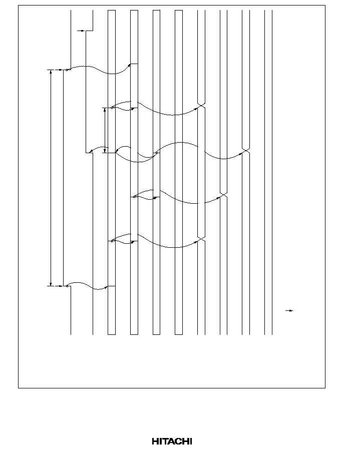
345
ADST
ADF
State of channel 0
(AN )
0
1
2
3
Continuous A/D conversion
Set
Clear
*
1
Clear
*
1
Idle
A/D conversion
Idle
Idle
Idle
A/D conversion
Idle
A/D conversion
Idle
A/D conversion
Idle
A/D conversion
Idle
Idle
Transfer
A/D conversion result
A/D conversion result
A/D conversion result
A/D conversion result
*
1
*
2
A/D conversion time
Notes:
*
2
(1)
(2)
(4)
(5)
*
1
(3)
(1)
(4)
(2)
(3)
ADDRA
ADDRB
ADDRC
ADDRD
State of channel 1
(AN )
State of channel 2
(AN )
State of channel 3
(AN )
Vertical arrows ( ) indicate instructions executed by software.
Data currently being converted is ignored.
Figure 15.4 Example of A/D Converter Operation (Scan Mode, Channels AN
0
to AN
2
Selected)
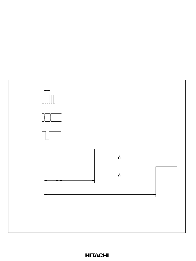
346
15.4.3
Input Sampling and A/D Conversion Time
The A/D converter has a built-in sample-and-hold circuit. The A/D converter samples the analog
input at a time t
D
after the ADST bit is set to 1, then starts conversion. Figure 15.5 shows the A/D
conversion timing. Table 15.4 indicates the A/D conversion time.
As indicated in figure 15.5, the A/D conversion time includes t
D
and the input sampling time. The
length of t
D
varies depending on the timing of the write access to ADCSR. The total conversion
time therefore varies within the ranges indicated in table 15.4.
In scan mode, the values given in table 15.4 apply to the first conversion. In the second and
subsequent conversions the conversion time is fixed at 256 states when CKS = 0 or 128 states
when CKS = 1. (when ¯
P
= ¯)
¯
Address bus
Write signal
Input sampling
timing
ADF
(1)
(2)
t
D
t
SPL
t
CONV
Legend:
(1):
(2):
t :
t :
t :
D
SPL
CONV
ADCSR write cycle
ADCSR address
Synchronization delay
Input sampling time
A/D conversion time
Figure 15.5 A/D Conversion Timing
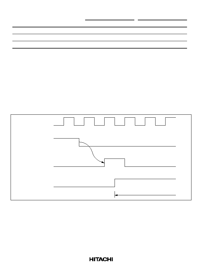
347
Table 15.4
A/D Conversion Time (Single Mode)
CKS = 0CKS = 1
Symbol
Min
Typ
Max
Min
Typ
Max
Synchronization delay
t
D
1
0
--
1
7
6
--
9
Input sampling time
*
t
SPL
--
80
--
--
40
--
A/D conversion time
*
t
CONV
259
--
266
131
--
134
Note:
*
Values in the table are numbers of states. Values are for ¯P = ¯. When ¯P = ¯/2, the
values are doubled.
15.4.4
External Trigger Input Timing
A/D conversion can be externally triggered. When the TRGE bit is set to 1 in ADCR, external
trigger input is enabled at the
ADTRG pin. A high-to-low transition at the ADTRG pin sets the
ADST bit to 1 in ADCSR, starting A/D conversion. Other operations, in both single and scan
modes, are the same as if the ADST bit had been set to 1 by software. Figure 15.6 shows the
timing.
¯
ADTRG
Internal trigger
signal
ADST
A/D conversion
Figure 15.6 External Trigger Input Timing

348
15.5
Interrupts
The A/D converter generates an interrupt (ADI) at the end of A/D conversion. The ADI interrupt
request can be enabled or disabled by the ADIE bit in ADCSR.
15.6
Useage Notes
When using the A/D converter, note the following points:
15.6.1
Setting Ranges of Analog Power Supply Pins, Etc.
Analog Input Voltage Range: The voltage applied to analog input pins AN
n
during A/D
conversion should be in the range AV
SS
AN
n
AV
CC
(n = 0 to 7).
AV
CC
and AV
SS
Input Voltages: For the AV
CC
input voltage, set AV
SS
= V
SS
. When the A/D
converter is not used, set AV
CC
= V
CC
and AV
SS
= V
SS
.
15.6.2
Notes on Board Design
In board design, digital circuitry and analog circuitry should be as mutually isolated as possible,
and layout in which digital circuit signal lines and analog circuit signal lines cross or are in close
proximity should be avoided as far as possible. Failure to do so may result in incorrect operation
of the analog circuitry due to inductance, adversely affecting A/D conversion values.
Also, digital circuitry must be isolated from the analog input signals (AN
0
to AN
7
), analog
reference voltage (AV
ref
), and analog power supply (AV
CC
) by the analog ground (AV
SS
). The
analog ground (AV
SS
) should be connected to a stable digital ground (V
SS
) at one point on the
board.
15.6.3
Notes on Noise
A protection circuit should be connected between AV
CC
and AV
SS
as shown in figure 15.7 to
prevent damage due to an abnormal voltage such as an excessive surge at the analog input pins
(AN
0
to AN
7
).
Also, the bypass capacitors connected to AV
CC
and AV
ref
and the filter capacitors connected to
AN
0
to AN
7
must be connected to AV
SS
.
If filter capacitors are connected as shown in figure 15.7, the input currents at the analog input
pins (AN
0
to AN
7
) will be smoothed, which may give rise to error. Error can also occur if A/D
conversion is frequently performed in scan mode so that the current that charges and discharges
the capacitor in the sample-and-hold circuit of the A/D converter becomes greater than that input

349
to the analog input pins via the input impedance (R
in
). The circuit constants should therefore be
selected carefully.
AV
CC
*
1
AN
0
to AN
7
AV
SS
*
2 R
in
: Input impedance
R
in
*
2
100
0.1
µ
F
0.01
µ
F
10
µ
F
*
1
Notes: Figures are reference values.
Figure 15.7 Example of Analog Input Pin Protection Circuit
15.6.4
A/D Conversion Accuracy Definitions
A/D conversion accuracy definitions for the H8/3397 Series are given below.
∑
Resolution
The number of A/D converter digital conversion output codes
∑
Offset error
The deviation of the analog input voltage value from the ideal A/D conversion characteristic
when the digital output changes from minimum voltage value B'0000000000 (H'000) to
B'0000000001 (H'001) (see figure 15.9).
∑
Full-scale error
The deviation of the analog input voltage value from the ideal A/D conversion characteristic
when the digital output changes from B'1111111110 (H'3FE) to B'1111111111 (H'3FF) (see
figure 15.9).
∑
Quantization error
The deviation inherent in the A/D converter, given by 1/2 LSB (see figure 15.8).
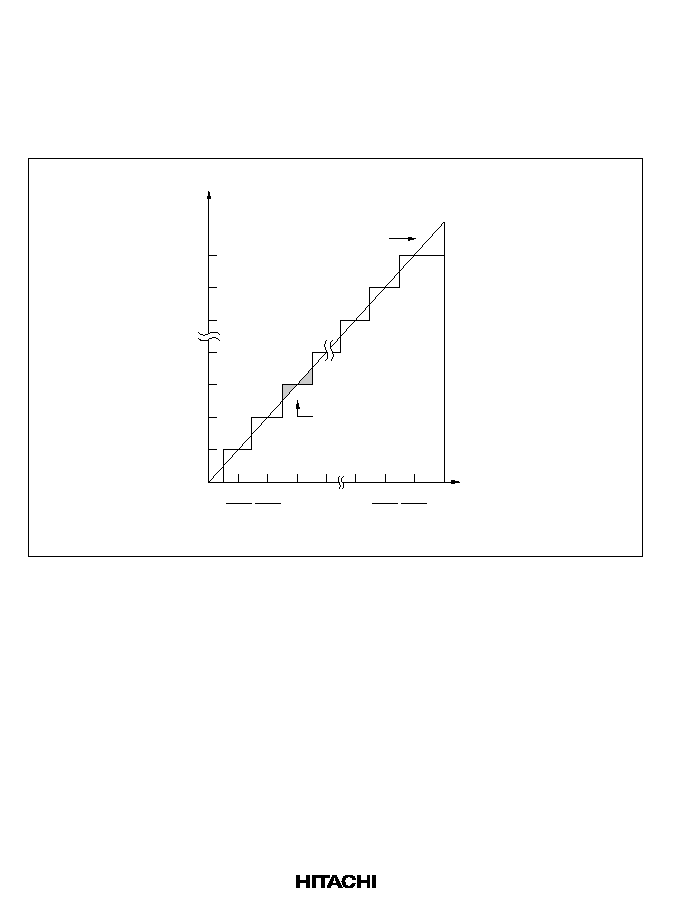
350
∑
Nonlinearity error
The error with respect to the ideal A/D conversion characteristic between the zero voltage and
the full-scale voltage. Does not include offset error, full-scale error, or quantization error.
∑
Absolute accuracy
The deviation between the digital value and the analog input value. Includes offset error, full-
scale error, quantization error, and nonlinearity error.
H'3FF
H'3FE
H'3FD
H'004
H'003
H'002
H'001
H'000
1
1024
2
1024
1022
1024
1023
1024
FS
Quantization error
Digital output
Ideal A/D conversion
characteristic
Analog input
voltage
Figure 15.8 A/D Conversion Accuracy Definitions (1)
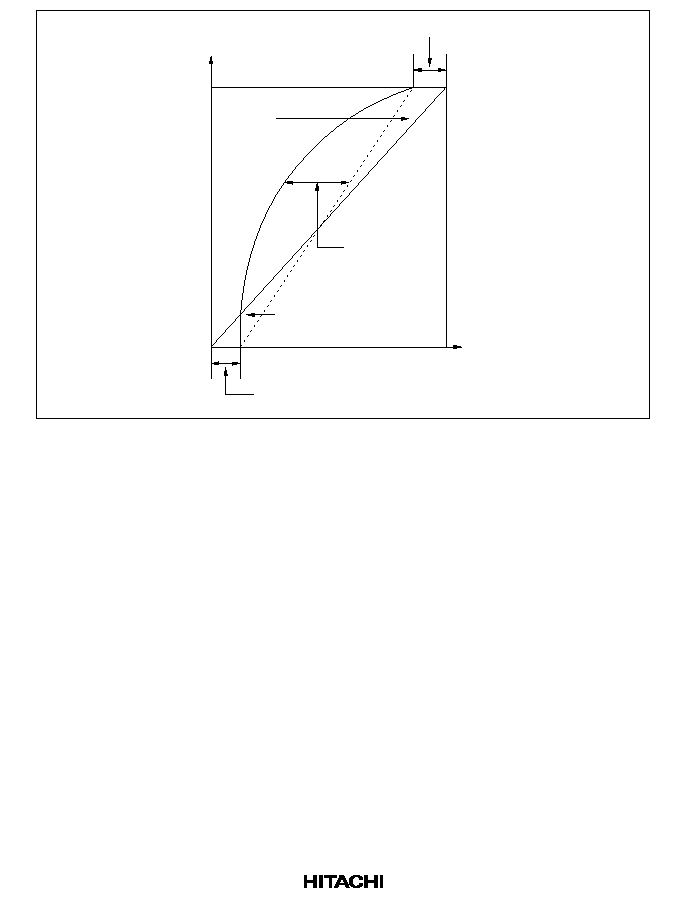
351
FS
Offset error
Nonlinearity
error
Actual A/D conversion
characteristic
Analog input
voltage
Digital output
Ideal A/D
conversion
characteristic
Full-scale error
Figure 15.9 A/D Conversion Accuracy Definitions (2)
15.6.5
Allowable Signal-Source Impedance
The analog inputs of the H8/3337 Series and H8/3397 Series are designed to assure accurate
conversion of input signals with a signal-source impedance not exceeding 10 k
. The reason for
this rating is that it enables the input capacitor in the sample-and-hold circuit in the A/D converter
to charge within the sampling time. If the sensor output impedance exceeds 10 k
, charging may
be inadequate and the accuracy of A/D conversion cannot be guaranteed.
If a large external capacitor is provided, then the internal 10 k
input resistance becomes the only
significant load on the input. In this case the impedance of the signal source is not a problem.
A large external capacitor, however, acts as a low-pass filter. This may make it impossible to track
analog signals with a large differential coefficient (e.g. 5 mV/µs or more).
To convert high-speed analog signals, insert a low-impedance buffer.

352
15.6.6
Effect on Absolute Accuracy
Attaching an external capacitor creates a coupling with ground, so if there is noise on the ground
line, it may degrade absolute accuracy. The capacitor must be connected to an electrically stable
ground, such as AV
SS
.
If a filter circuit is used, be careful of interference with digital signals on the same board, and
make sure the circuit does not act as an antenna.
Equivalent circuit of A/D
converter
H8/3337 Series
or H8/3397
Series chip
20 pF
C
in
=
15 pF
10 k
up to 10 k
Low-pass
filter C,
up to 0.1
µ
F
Sensor output
impedance,
Sensor input
Note: Figures are reference values.
Figure 15.10 Example of Analog Input Circuit

353
Section 16 D/A Converter (H8/3337 Series Only)
16.1
Overview
The H8/3337 Series has an on-chip D/A converter module with two channels.
16.1.1
Features
Features of the D/A converter module are listed below.
∑
Eight-bit resolution
∑
Two-channel output
∑
Maximum conversion time: 10 µs (with 20-pF load capacitance)
∑
Output voltage: 0 V to AV
CC
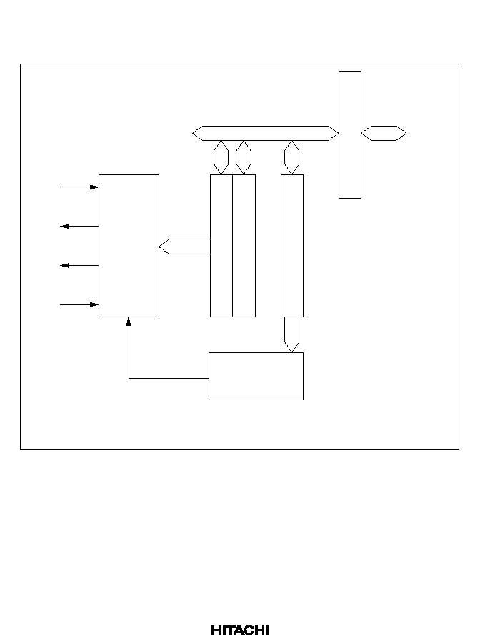
354
16.1.2
Block Diagram
Figure 16.1 shows a block diagram of the D/A converter.
Bus interface
Module data bus
Internal data bus
8-bit D/A
DADR0
DADR1
DACR
Control
circuit
AV
DA
DA
AV
CC
0
1
SS
DACR:
DADR0:
DADR1:
D/A control register
D/A data register 0
D/A data register 1
Figure 16.1 D/A Converter Block Diagram

355
16.1.3
Input and Output Pins
Table 16.1 lists the input and output pins used by the D/A converter module.
Table 16.1
Input and Output Pins of D/A Converter Module
Name
Abbreviation
I/O
Function
Analog supply voltage
AV
CC
Input
Power supply and reference voltage for
analog circuits
Analog ground
AV
SS
Input
Ground and reference voltage for analog
circuits
Analog output 0
DA
0
Output
Analog output channel 0
Analog output 1
DA
1
Output
Analog output channel 1
16.1.4
Register Configuration
Table 16.2 lists the three registers of the D/A converter module.
Table 16.2
D/A Converter Registers
Name
Abbreviation
R/W
Initial Value
Address
D/A data register 0
DADR0
R/W
H'00
H'FFF8
D/A data register 1
DADR1
R/W
H'00
H'FFF9
D/A control register
DACR
R/W
H'1F
H'FFFA

356
16.2
Register Descriptions
16.2.1
D/A Data Registers 0 and 1 (DADR0, DADR1)
Bit
7
6
5
4
3
2
1
0
Initial value
0
0
0
0
0
0
0
0
Read/Write
R/W
R/W
R/W
R/W
R/W
R/W
R/W
R/W
D/A data registers 0 and 1 (DADR0 and DADR1) are 8-bit readable and writable registers that
store data to be converted. When analog output is enabled, the value in the D/A data register is
converted and output continuously at the analog output pin.
The D/A data registers are initialized to H'00 at a reset and in the standby modes.
16.2.2
D/A Control Register (DACR)
Bit
7
6
5
4
3
2
1
0
DAOE1
DAOE0
DAE
--
--
--
--
--
Initial value
0
0
0
1
1
1
1
1
Read/Write
R/W
R/W
R/W
--
--
--
--
--
DACR is an 8-bit readable and writable register that controls the operation of the D/A converter
module.
DACR is initialized to H'1F at a reset and in the standby modes.
Bit 7--D/A Output Enable 1 (DAOE1): Controls analog output from the D/A converter.
Bit 7: DAOE1
Description
0
Analog output at DA
1
is disabled.
1
D/A conversion is enabled on channel 1. Analog output is enabled at DA
1
.

357
Bit 6--D/A Output Enable 0 (DAOE0): Controls analog output from the D/A converter.
Bit 6: DAOE0
Description
0
Analog output at DA
0
is disabled.
1
D/A conversion is enabled on channel 0. Analog output is enabled at DA
0
.
Bit 5--D/A Enable (DAE): Controls D/A conversion, in combination with bits DAOE0 and
DAOE1. D/A conversion is controlled independently on channels 0 and 1 when DAE = 0.
Channels 0 and 1 are controlled together when DAE = 1.
The decision to output the converted results is always controlled independently by DAOE0 and
DAOE1.
Bit 7: DAOE1
Bit 6: DAOE0
Bit 5: DAE
Description
0
0
--
Disabled on channels 0 and 1.
1
0
Enabled on channel 0.
Disabled on channel 1.
1
Enabled on channels 0 and 1.
1
0
0
Disabled on channel 0.
Enabled on channel 1.
1
Enabled on channels 0 and 1.
1
--
Enabled on channels 0 and 1.
When the DAE bit is set to 1, analog power supply current drain is the same as during A/D and
D/A conversion, even if the DAOE0 and DAOE1 bits in DACR and the ADST bit in ADSCR are
cleared to 0.
Bits 4 to 0--Reserved: These bits cannot be modified and are always read as 1.

358
16.3
Operation
The D/A converter module has two built-in D/A converter circuits that can operate independently.
D/A conversion is performed continuously whenever enabled by the D/A control register. When a
new value is written in DADR0 or DADR1, conversion of the new value begins immediately. The
converted result is output by setting the DAOE0 or DAOE1 bit to 1.
An example of conversion on channel 0 is given next. Figure 16.2 shows the timing.
1. Software writes the data to be converted in DADR0.
2. D/A conversion begins when the DAOE0 bit in DACR is set to 1. After a conversion delay,
analog output appears at the DA0 pin. The output value is AV
CC
◊
(DADR0 value)/256.
This output continues until a new value is written in DADR0 or the DAOE0 bit is cleared to 0.
3. If a new value is written in DADR0, conversion begins immediately. Output of the converted
result begins after the conversion delay time.
4. When the DAOE0 bit is cleared to 0, DA0 becomes an input pin.
DADR0
write cycle
DACR
write cycle
DADR0
write cycle
DACR
write cycle
Address
¯
DADR0
DAOE0
DA0
Conversion data (1)
Conversion data (2)
High-impedance state
Conversion result (1)
Conversion result (2)
t
DCONV
t
DCONV
t :
D/A conversion time
DCONV
Figure 16.2 D/A Conversion (Example)

359
Section 17 RAM
17.1
Overview
The H8/3337Y, H8/3336Y, H8/3397, and H8/3396 have 2 kbytes of on-chip static RAM. The
H8/3334Y and H8/3394 have 1 kbyte. The RAM is connected to the CPU by a 16-bit data bus.
Both byte and word access to the on-chip RAM are performed in two states, enabling rapid data
transfer and instruction execution.
The on-chip RAM is assigned to addresses H'F780 to H'FF7F in the address space of the
H8/3337Y, H8/3336Y, H8/3397, and H8/3396 and addresses H'FB80 to H'FF7F in the address
space of the H8/3334Y and H8/3394. The RAME bit in the system control register (SYSCR) can
enable or disable the on-chip RAM.
17.1.1
Block Diagram
Figure 17.1 is a block diagram of the on-chip RAM.
H'FF7E
Internal data bus (upper 8 bits)
H'FF7F
H'F782
H'F780
H'F783
H'F781
Even address
Odd address
On-chip RAM
Internal data bus (lower 8 bits)
Figure 17.1 Block Diagram of On-Chip RAM (H8/3337Y)

360
17.1.2
RAM Enable Bit (RAME) in System Control Register (SYSCR)
Bit
7
6
5
4
3
2
1
0
SSBY
STS2
STS1
STS0
XRST
NMIEG
HIE
RAME
Initial value
0
0
0
0
1
0
0
1
Read/Write
R/W
R/W
R/W
R/W
R
R/W
R/W
R/W
The on-chip RAM is enabled or disabled by the RAME bit in SYSCR. See section 3.2, System
Control Register, for the other SYSCR bits.
Bit 0--RAM Enable (RAME): This bit enables or disables the on-chip RAM. The RAME bit is
initialized to 1 on the rising edge of the
RES signal. The RAME bit is not initialized in software
standby mode.
Bit 0: RAME
Description
0
On-chip RAM is disabled.
1
On-chip RAM is enabled.
(Initial value)
17.2
Operation
17.2.1
Expanded Modes (Modes 1 and 2)
If the RAME bit is set to 1, accesses to addresses H'F780 to H'FF7F in the H8/3337Y, H8/3336Y,
H8/3397, and H8/3396 and addresses H'FB80 to H'FF7F in the H8/3334Y and H8/3394 are
directed to the on-chip RAM. If the RAME bit is cleared to 0, accesses to these addresses are
directed to the external data bus.
17.2.2
Single-Chip Mode (Mode 3)
If the RAME bit is set to 1, accesses to addresses H'F780 to H'FF7F in the H8/3337Y, H8/3336Y,
H8/3397, and H8/3396 and addresses H'FB80 to H'FF7F in the H8/3334Y and H8/3394 are
directed to the on-chip RAM.
If the RAME bit is cleared to 0, the on-chip RAM data cannot be accessed. Attempted write access
has no effect. Attempted read access always results in H'FF data being read.
Notes: 1. When V
CC
V
RAM
, on-chip RAM values can be retained by using the specified method.
See section 21.4.1 and Appendix E for details.
2. On-chip RAM values are not guaranteed if power is turned off, then on again, in any
state.
3. When specific bits in RAM are used as control bits, initial values must be set after
powering on.

361
Section 18 ROM (Mask ROM Version/ZTAT Version)
18.1
Overview
The size of the on-chip ROM is 60 kbytes in the H8/3337Y and H8/3397, 48 kbytes in the
H8/3336Y and H8/3396, and 32 kbytes in the H8/3334Y and H8/3394. The on-chip ROM is
connected to the CPU via a 16-bit data bus. Both byte data and word data are accessed in two
states, enabling rapid data transfer.
The on-chip ROM is enabled or disabled depending on the inputs at the mode pins (MD
1
and
MD
0
). See table 18.1.
Table 18.1
On-Chip ROM Usage in Each MCU Operating Mode
Mode Pins
Mode
MD
1
MD
0
On-Chip ROM
Mode 1 (expanded mode)
0
1
Disabled (external addresses)
Mode 2 (expanded mode)
1
0
Enabled
Mode 3 (single-chip mode)
1
1
Enabled
The PROM versions (H8/3337Y ZTAT and H8/3334Y ZTAT) can be set to writer mode and
programmed with a general-purpose PROM programmer. In the H8/3337Y and H8/3397, the
accessible ROM addresses are H'0000 to H'EF7F (61,312 bytes) in mode 2, and H'0000 to H'F77F
(63,360 bytes) in mode 3. For details, see section 3, MCU Operating Modes and Address Space.
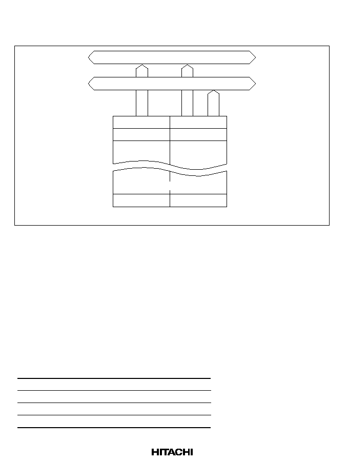
362
18.1.1
Block Diagram
Figure 18.1 is a block diagram of the on-chip ROM.
H'F77E
Internal data bus (upper 8 bits)
H'F77F
H'0002
H'0000
H'0003
H'0001
Even address
Odd address
On-chip ROM
Internal data bus (lower 8 bits)
Figure 18.1 Block Diagram of On-Chip ROM (H8/3337Y Single-Chip Mode)
18.2
Writer Mode (H8/3337Y, H8/3334Y)
18.2.1
Writer Mode Setup
In writer mode the PROM versions of the H8/3337Y and H8/3334Y suspend the usual
microcomputer functions to allow the on-chip PROM to be programmed. The programming
method is the same as for the HN27C101, except that page programming is not supported.
To select writer mode, apply the signal inputs listed in table 18.2.
Table 18.2
Selection of Writer Mode
Pin
Input
Mode pin MD
1
Low
Mode pin MD
0
Low
STBY
pin
Low
Pins P6
3
and P6
4
High

363
18.2.2
Socket Adapter Pin Assignments and Memory Map
The H8/3337Y and H8/3334Y can be programmed with a general-purpose PROM programmer by
using a socket adapter to change the pin-out to 32 pins. See table 18.3. The same socket adapter
can be used for both the H8/3337Y and H8/3334Y. Figure 18.2 shows the socket adapter pin
assignments.
Table 18.3
Socket Adapter
Package
Socket Adapter
80-pin QFP
HS3337ESHS1H
80-pin TQFP
HS3337ESNS1H
84-pin PLCC
HS3337ESCS1H
84-pin windowed LCC
HS3337ESGS1H
The PROM size is 60 kbytes for the H8/3337Y and 32 kbytes for the H8/3334Y. Figures 18.3 and
18.4 show memory maps of the H8/3337Y and H8/3334Y in writer mode. H'FF data should be
specified for unused address areas in the on-chip PROM.
When programming with a PROM programmer, limit the program address range to H'0000 to
H'F77F for the H8/3337Y and H'0000 to H'7FFF for the H8/3334Y. Specify H'FF data for
addresses H'F780 and above (H8/3337Y) or H'8000 and above (H8/3334Y). If these addresses are
programmed by mistake, it may become impossible to program or verify the PROM data. The
same problem may occur if an attempt is made to program the chip in page programming mode.
Note that the PROM versions are one-time programmable (OTP) microcomputers, packaged in
plastic packages, and cannot be reprogrammed.
364
1
6
65
66
67
68
69
70
71
72
64
63
62
61
60
59
58
57
55
54
53
52
51
50
49
48
20
19
18
24
25
29
8, 47
5
4
7
38
12, 56,
73
RES
NMI
P3
P3
P3
P3
P3
P3
P3
P3
P1
P1
P1
P1
P1
P1
P1
P1
P2
P2
P2
P2
P2
P2
P2
P2
P9
P9
P9
P6
P6
AV
V
CC
MD
MD
STBY
AV
V
V
EA
EO
EO
EO
EO
EO
EO
EO
EO
EA
EA
EA
EA
EA
EA
EA
EA
EA
OE
EA
EA
EA
EA
EA
CE
EA
EA
PGM
V
V
HN27C101
(32 pins)
1
26
13
14
15
17
18
19
20
21
12
11
10
9
8
7
6
5
27
24
23
25
4
28
29
22
2
3
31
32
16
0
1
2
3
4
5
6
7
0
1
2
3
4
5
6
7
0
1
2
3
4
5
6
7
0
1
2
3
4
CC
0
1
SS
SS
9
0
1
2
3
4
5
6
7
0
1
2
3
4
5
6
7
8
10
11
12
13
14
16
15
PP
CC
H8/3337Y, H8/3334Y
EPROM Socket
Note: All pins not listed in this figure should be left open.
V
PP
:
EO
7
to EO
0
:
EA
16
to EA
0
:
OE
:
CE
:
PGM
:
Program voltage (12.5 V)
Data input/output
Address input
Output enable
Chip enable
Program enable
SS
FP-80A
TFP-80C
12
17
79
80
81
82
83
84
1
3
78
77
76
75
74
73
72
71
69
68
67
66
65
63
62
61
32
31
30
36
37
42
19, 60
16
15
18
51
2, 4, 23,
24, 41,
64, 70
CP-84
CG-84
Pin
Pin
Figure 18.2 Socket Adapter Pin Assignments
365
H'F77F
H'F77F
Undefined
value output
*
If this address area is read in writer mode, the output data is not guaranteed.
H'1FFFF
Address in writer mode
Address in MCU mode
H'0000
H'0000
On-chip
PROM
Note:
*
Figure 18.3 H8/3337Y Memory Map in Writer Mode
H'7FFF
H'7FFF
Undefined
value output
*
If this address area is read in writer mode, the output data is not guaranteed.
H'1FFFF
Address in writer mode
Address in MCU mode
H'0000
H'0000
On-chip
PROM
Note:
*
Figure 18.4 H8/3334Y Memory Map in Writer Mode

366
18.3
PROM Programming
The write, verify, and other sub-modes of the writer mode are selected as shown in table 18.4.
Table 18.4
Selection of Sub-Modes in Writer Mode
Sub-Mode
CE
OE
PGM
V
PP
V
CC
EO
7
to EO
0
EA
16
to EA
0
Write
Low
High
Low
V
PP
V
CC
Data input
Address input
Verify
Low
Low
High
V
PP
V
CC
Data output
Address input
Programming
inhibited
Low
Low
High
High
Low
High
Low
High
Low
High
Low
High
V
PP
V
CC
High impedance
Address input
Legend:
V
PP
: V
PP
level
V
CC
: V
CC
level
The H8/3337Y and H8/3334Y PROM have the same standard read/write specifications as the
HN27C101 EPROM. Page programming is not supported, however, so do not select page
programming mode. PROM programmers that provide only page programming cannot be used.
When selecting a PROM programmer, check that it supports a byte-at-a-time high-speed
programming mode. Be sure to set the address range to H'0000 to H'F77F for the H8/3337Y, and
to H'0000 to H'7FFF for the H8/3334Y.
18.3.1
Programming and Verification
An efficient, high-speed programming procedure can be used to program and verify PROM data.
This procedure programs data quickly without subjecting the chip to voltage stress and without
sacrificing data reliability. It leaves the data H'FF in unused addresses.
Figure 18.5 shows the basic high-speed programming flowchart.
Tables 18.5 and 18.6 list the electrical characteristics of the chip in writer mode. Figure 18.6
shows a program/verify timing chart.
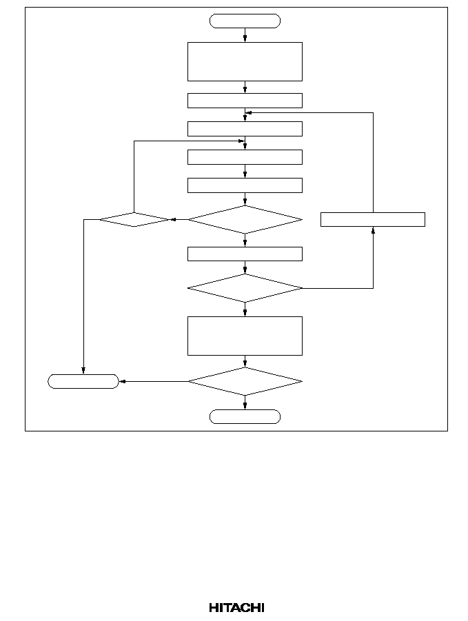
367
Start
Set program/verify mode
V
CC
= 6.0 V
±
0.25 V,
V
PP
= 12.5 V
±
0.3 V
Address = 0
Verify OK?
Program t
OPW
= 0.2n ms
Last address?
Set read mode
V
CC
= 5.0 V
±
0.25 V,
V
PP
= V
CC
Read all
addresses
End
Error
n
<
25?
Address + 1 address
No
Yes
No
Yes
No
No go
Program t
PW
= 0.2 ms
±
5%
n = 0
n + 1 n
Yes
Go
Figure 18.5 High-Speed Programming Flowchart

368
Table 18.5
DC Characteristics
(when V
CC
= 6.0 V ±0.25 V, V
PP
= 12.5 V ±0.3 V, V
SS
= 0 V, Ta = 25∞C ±5∞C)
Item
Symbol
Min
Typ
Max
Unit
Test Conditions
Input high
voltage
EO
7
≠EO
0
,
EA
16
≠EA
0
,
OE
,
CE
,
PGM
V
IH
2.4
--
V
CC
+ 0.3
V
Input low
voltage
EO
7
≠ EO
0
,
EA
16
≠ EA
0
,
OE
,
CE
,
PGM
V
IL
≠0.3
--
0.8
V
Output high
voltage
EO
7
≠EO
0
V
OH
2.4
--
--
V
I
OH
= ≠200 µA
Output low
voltage
EO
7
≠EO
0
V
OL
--
--
0.45
V
I
OL
= 1.6 mA
Input leakage
current
EO
7
≠ EO
0
,
EA
16
≠ EA
0
,
OE
,
CE
,
PGM
|I
LI
|
--
--
2
µA
V
in
= 5.25 V/0.5 V
V
CC
current
I
CC
--
--
40
mA
V
PP
current
I
PP
--
--
40
mA

369
Table 18.6
AC Characteristics
(when V
CC
= 6.0 V ±0.25 V, V
PP
= 12.5 V ±0.3 V, Ta = 25∞C ±5∞C)
Item
Symbol
Min
Typ
Max
Unit
Test Conditions
Address setup time
t
AS
2
--
--
µs
See figure 18.6
*
OE
setup time
t
OES
2
--
--
µs
Data setup time
t
DS
2
--
--
µs
Address hold time
t
AH
0
--
--
µs
Data hold time
t
DH
2
--
--
µs
Data output disable time
t
DF
--
--
130
ns
V
PP
setup time
t
VPS
2
--
--
µs
Program pulse width
t
PW
0.19
0.20
0.21
ms
OE
pulse width for
overwrite-programming
t
OPW
0.19
--
5.25
ms
V
CC
setup time
t
VCS
2
--
--
µs
CE
setup time
t
CES
2
--
--
µs
Data output delay time
t
OE
0
--
150
ns
Note:
*
Input pulse level: 0.8 V to 2.2 V
Input rise/fall time
20 ns
Timing reference levels: input--1.0 V, 2.0 V; output--0.8 V, 2.0 V

370
Address
Data
V
PP
V
CC
CE
PGM
OE
V
PP
V
CC
V
CC
V
CC
Write
Verify
Input data
Output data
t
AS
t
DS
t
VPS
t
VCS
t
CES
t
PW
t
OPW
t
DH
t
OES
t
OE
t
DF
t
AH
+ 1
Figure 18.6 PROM Program/Verify Timing

371
18.3.2
Notes on Programming
(1) A PROM programmer that does not allow start address setting cannot be used. If such a
PROM programmer is used, it will not be possible to perform verification at addresses H'10002,
H'10003, H'10004, and so on. Therefore a PROM programmer that allows address setting must be
used.
(2) Program with the specified voltages and timing. The programming voltage (V
PP
) is
12.5 V.
Caution: Applied voltages in excess of the specified values can permanently destroy the chip. Be
particularly careful about the PROM programmer's overshoot characteristics.
If the PROM programmer is set to HN27C101 specifications, V
PP
will be 12.5 V.
(3) Before writing data, check that the socket adapter and chip are correctly mounted in the
PROM writer. Overcurrent damage to the chip can result if the index marks on the PROM
programmer, socket adapter, and chip are not correctly aligned.
(4) Don't touch the socket adapter or chip while writing. Touching either of these can cause
contact faults and write errors.
(5) Page programming is not supported. Do not select page programming mode.
(6) The H8/3337Y PROM size is 60 kbytes. The H8/3334Y PROM size is 32 kbytes. Set the
address range to H'0000 to H'F77F for the H8/3337Y, and to H'0000 to H'7FFF for the H8/3334Y.
When programming, specify H'FF data for unused address areas (H'F780 to H'1FFFF in the
H8/3337Y, H'8000 to H'1FFFF in the H8/3334Y).
18.3.3
Reliability of Programmed Data
An effective way to assure the data holding characteristics of the programmed chips is to bake
them at 150∞C, then screen them for data errors. This procedure quickly eliminates chips with
PROM memory cells prone to early failure.
Figure 18.7 shows the recommended screening procedure.
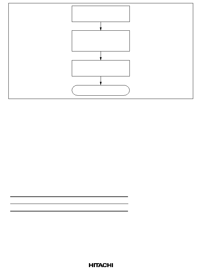
372
Read and check program
Install
Bake with power off
125
∞
C to 150
∞
C,
24 Hr to 48 Hr
Write and verify program
Figure 18.7 Recommended Screening Procedure
If a series of write errors occurs while the same PROM programmer is in use, stop programming
and check the PROM programmer and socket adapter for defects, using a microcontroller with on-
chip EPROM in a windowed package, for instance.
Please inform Hitachi of any abnormal conditions noted during programming or in screening of
program data after high-temperature baking.
18.3.4
Erasing Data
Data is erased by exposing the transparent window in the package to ultraviolet light. The erase
conditions are shown in table 18.7.
Table 18.7
Erase Conditions
Item
Value
Ultraviolet wavelength
253.7nm
Minimum irradiation
15W ∑ s/cm
2
The erase conditions in table 18.7 can be met by exposure to a 12000 µW/cm
2
ultraviolet lamp
positioned 2 to 3 cm directly above the chip for approximately 20 minutes.
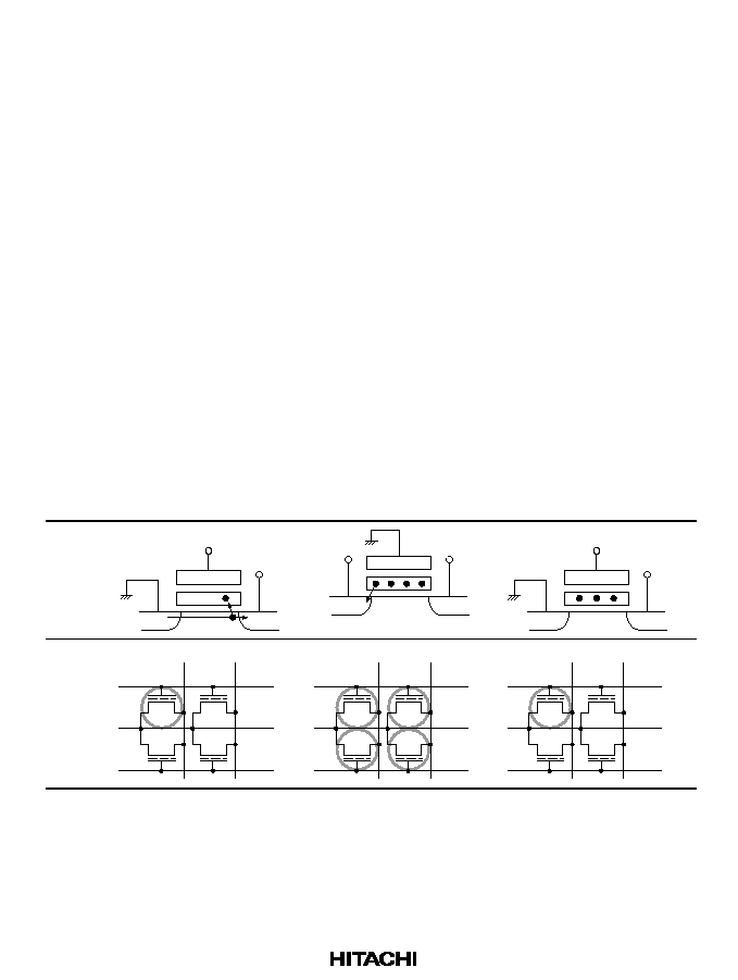
373
Section 19 ROM
(32-kbyte Dual-Power-Supply Flash Memory Version)
19.1
Flash Memory Overview
19.1.1
Flash Memory Operating Principle
Table 19.1 illustrates the principle of operation of the H8/3334YF's on-chip flash memory.
Like EPROM, flash memory is programmed by applying a high gate-to-drain voltage that draws
hot electrons generated in the vicinity of the drain into a floating gate. The threshold voltage of a
programmed memory cell is therefore higher than that of an erased cell. Cells are erased by
grounding the gate and applying a high voltage to the source, causing the electrons stored in the
floating gate to tunnel out. After erasure, the threshold voltage drops. A memory cell is read like
an EPROM cell, by driving the gate to the high level and detecting the drain current, which
depends on the threshold voltage. Erasing must be done carefully, because if a memory cell is
overerased, its threshold voltage may become negative, causing the cell to operate incorrectly.
Section 19.4.6 shows an optimal erase control flowchart and sample program.
Table 19.1
Principle of Memory Cell Operation
Program
Erase
Read
Memory
cell
Vd
Vg = V
PP
Open
Vs = V
PP
Vd
Vg
Memory
array
Vd
0 V
V
PP
0 V
0 V
Open
Open
0 V
V
PP
0 V
Vd
0 V
V
CC
0 V
0 V

374
19.1.2
Mode Programming and Flash Memory Address Space
As its on-chip ROM, the H8/3334YF has 32 kbytes of flash memory. The flash memory is
connected to the CPU by a 16-bit data bus. The CPU accesses both byte data and word data in two
states.
The H8/3334YF's flash memory is assigned to addresses H'0000 to H'7FFF. The mode pins
enable either on-chip flash memory or external memory to be selected for this area. Table 19.2
summarizes the mode pin settings and usage of the memory area.
Table 19.2
Mode Pin Settings and Flash Memory Area
Mode Pin Setting
Mode
MD
1
MD
0
Memory Area Usage
Mode 0
0
0
Illegal setting
Mode 1
0
1
External memory area
Mode 2
1
0
On-chip flash memory area
Mode 3
1
1
On-chip flash memory area
19.1.3
Features
Features of the flash memory are listed below.
∑
Five flash memory operating modes
The flash memory has five operating modes: program mode, program-verify mode, erase
mode, erase-verify mode, and prewrite-verify mode.
∑
Block erase designation
Blocks to be erased in the flash memory address space can be selected by bit settings. The
address space includes a large-block area (four blocks with sizes from 4 kbytes to 8 kbytes)
and a small-block area (eight blocks with sizes from 128 bytes to 1 kbyte).
∑
Program and erase time
Programming one byte of flash memory typically takes 50 µs, while erasing typically takes 1 s.
∑
Erase-program cycles
Flash memory contents can be erased and reprogrammed up to 100 times.
∑
On-board programming modes
These modes can be used to program, erase, and verify flash memory contents. There are two
modes: boot mode and user programming mode.
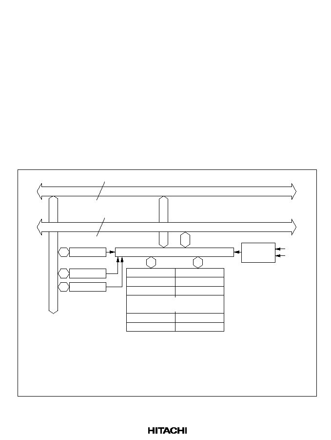
375
∑
Automatic bit-rate alignment
In boot-mode data transfer, the H8/3334YF aligns its bit rate automatically to the host bit rate
(maximum 9600 bps).
∑
Flash memory emulation by RAM
Part of the RAM area can be overlapped onto flash memory, to emulate flash memory updates
in real time.
∑
Writer mode
As an alternative to on-board programming, the flash memory can be programmed and erased
in writer mode, using a general-purpose PROM programmer. Program, erase, verify, and other
specifications are the same as for HN28F101 standard flash memory.
19.1.4
Block Diagram
Figure 19.1 shows a block diagram of the flash memory.
FLMCR
EBR1
EBR2
H'0000
H'0002
H'0004
H'7FFC
H'7FFE
H'0001
H'0003
H'0005
H'7FFD
H'7FFF
MD
1
MD
0
Internal data bus (upper)
Internal data bus (lower)
Bus interface and control section
Operating
mode
On-chip flash memory
(32 kbytes)
Upper byte
(even address)
Lower byte
(odd address)
Legend:
FLMCR:
EBR1:
EBR2:
Flash memory control register
Erase block register 1
Erase block register 2
8
8
Figure 19.1 Flash Memory Block Diagram

376
19.1.5
Input/Output Pins
Flash memory is controlled by the pins listed in table 19.3.
Table 19.3
Flash Memory Pins
Pin Name
Abbreviation
Input/Output
Function
Programming power
FV
PP
Power supply
Apply 12.0 V
Mode 1
MD
1
Input
H8/3334YF operating mode setting
Mode 0
MD
0
Input
H8/3334YF operating mode setting
Transmit data
TxD
1
Output
SCI1 transmit data output
Receive data
RxD
1
Input
SCI1 receive data input
The transmit data and receive data pins are used in boot mode.
19.1.6
Register Configuration
The flash memory is controlled by the registers listed in table 19.4.
Table 19.4
Flash Memory Registers
Name
Abbreviation
R/W
Initial Value
Address
Flash memory control register
FLMCR
R/W
*
2
H'00
*
2
H'FF80
Erase block register 1
EBR1
R/W
*
2
H'F0
*
2
H'FF82
Erase block register 2
EBR2
R/W
*
2
H'00
*
2
H'FF83
Wait-state control register
*
1
WSCR
R/W
H'08
H'FFC2
Notes:
*
1 The wait-state control register controls the insertion of wait states by the wait-state
controller, frequency division of clock signals for the on-chip supporting modules by the
clock pulse generator, and emulation of flash-memory updates by RAM in on-board
programming mode.
*
2 In modes 2 and 3 (on-chip flash memory enabled), the initial value is H'00 for FLMCR
and EBR2, and H'F0 for EBR1. In mode 1 (on-chip flash memory disabled), these
registers cannot be modified and always read H'FF.
Registers FLMCR, EBR1, and EBR2 are only valid when writing to or erasing flash memory, and
can only be accessed while 12 V is being applied to the FV
PP
pin.
When 12 V is not applied to the FV
PP
pin, in mode 2 addresses H'FF80 to H'FF83 are external
address space, and in mode 3 these addresses connot be modified and always read H'FF.

377
19.2
Flash Memory Register Descriptions
19.2.1
Flash Memory Control Register (FLMCR)
FLMCR is an 8-bit register that controls the flash memory operating modes. Transitions to
program mode, erase mode, program-verify mode, and erase-verify mode are made by setting bits
in this register. FLMCR is initialized to H'00 by a reset, in the standby modes, and when 12 V is
not applied to FV
PP
. When 12 V is applied to the FV
PP
pin, a reset or entry to a standby mode
initializes FLMCR to H'80.
Bit
7
6
5
4
3
2
1
0
V
PP
--
--
--
EV
PV
E
P
Initial value
0
0
0
0
0
0
0
0
Read/Write
R
--
--
--
R/W
*
R/W
*
R/W
*
R/W
*
Note:
*
The initial value is H'00 in modes 2 and 3 (on-chip flash memory enabled). In mode 1 (on-
chip flash memory disabled), this register cannot be modified and always reads H'FF. For
information on accessing this register, refer to in section 19.7, Flash Memory Programming
and Erasing Precautions (11).
Bit 7--Programming Power (V
PP
): This status flag indicates that 12 V is applied to the FV
PP
pin.
Refer to section 19.7, Flash Memory Programming and Erasing Precautions (5), for details on use.
Bit 7: V
PP
Description
0
Cleared when 12 V is not applied to FV
PP
(Initial value)
1
Set when 12 V is applied to FV
PP
Bits 6 to 4--Reserved: These bits cannot be modified, and are always read as 0.
Bit 3--Erase-Verify Mode (EV):
*1
Selects transition to or exit from erase-verify mode.
Bit 3: EV
Description
0
Exit from erase-verify mode
(Initial value)
1
Transition to erase-verify mode
Bit 2--Program-Verify Mode (PV):
*1
Selects transition to or exit from program-verify mode.
Bit 2: PV
Description
0
Exit from program-verify mode
(Initial value)
1
Transition to program-verify mode

378
Bit 1--Erase Mode (E):
*1, *2
Selects transition to or exit from erase mode.
Bit 1: E
Description
0
Exit from erase mode
(Initial value)
1
Transition to erase mode
Bit 0--Program Mode (P):
*1, *2
Selects transition to or exit from program mode.
Bit 0: P
Description
0
Exit from program mode
(Initial value)
1
Transition to program mode
Notes: *1 Do not set two or more of these bits simultaneously. Do not release or shut off the V
CC
or V
PP
power supply when these bits are set.
*2 Set the P or E bit according to the instructions given in section 19.4, Programming and
Erasing Flash Memory.
Set the watchdog timer beforehand to make sure that these bits do not remain set for
longer than the specified times.
For notes on use, see section 19.7, Flash Memory Programming and Erasing
Precautions.
19.2.2
Erase Block Register 1 (EBR1)
EBR1 is an 8-bit register that designates large flash-memory blocks for programming and erasure.
EBR1 is initialized to H'F0 by a reset, in the standby modes, and when 12 V is not applied to the
FV
PP
pin. When a bit in EBR1 is set to 1, the corresponding block is selected and can be
programmed and erased. Figure 19.2 and table 19.6 show details of a block map.
Bit
7
6
5
4
3
2
1
0
--
--
--
--
LB3
LB2
LB1
LB0
Initial value
1
1
1
1
0
0
0
0
Read/Write
--
--
--
--
R/W
*
R/W
*
R/W
*
R/W
*
Note:
*
The initial value is H'F0 in modes 2 and 3 (on-chip ROM enabled). In mode 1 (on-chip ROM
disabled), this register cannot be modified and always reads H'FF. For information on
accessing this register, refer to in section 19.7 Flash Memory Programming and erasing
Precautions (11).
379
Bits 7 to 4--Reserved: These bits cannot be modified, and are always read as 1.
Bits 3 to 0--Large Block 3 to 0 (LB3 to LB0): These bits select large blocks (LB3 to LB0) to be
programmed and erased.
Bits 3 to 0:
LB3 to LB0
Description
0
Block (LB3 to LB0) is not selected
(Initial value)
1
Block (LB3 to LB0) is selected
19.2.3
Erase Block Register 2 (EBR2)
EBR2 is an 8-bit register that designates small flash-memory blocks for programming and erasure.
EBR2 is initialized to H'00 by a reset, in the standby modes, and when 12 V is not applied to the
FV
PP
pin. When a bit in EBR2 is set to 1, the corresponding block is selected and can be
programmed and erased. Figure 19.2 and table 19.6 show a block map.
Bit
7
6
5
4
3
2
1
0
SB7
SB6
SB5
SB4
SB3
SB2
SB1
SB0
Initial value
0
0
0
0
0
0
0
0
Read/Write
R/W
*
R/W
*
R/W
*
R/W
*
R/W
*
R/W
*
R/W
*
R/W
*
Note:
*
The initial value is H'00 in modes 2 and 3 (on-chip ROM enabled). In mode 1 (on-chip ROM
disabled), this register cannot be modified and always reads H'FF. For information on
accessing this register, refer to in section 19.7 Flash Memory Programming and erasing
Precautions (11).
Bits 7 to 0--Small Block 7 to 0 (SB7 to SB0): These bits select small blocks (SB7 to SB0) to be
programmed and erased.
Bits 7 to 0:
SB7 to SB0
Description
0
Block (SB7 to SB0) is not selected
(Initial value)
1
Block (SB7 to SB0) is selected

380
19.2.4
Wait-State Control Register (WSCR)
WSCR is an 8-bit readable/writable register that enables flash-memory updates to be emulated in
RAM. It also controls frequency division of clock signals supplied to the on-chip supporting
modules and insertion of wait states by the wait-state controller.
WSCR is initialized to H'08 by a reset and in hardware standby mode. It is not initialized in
software standby mode.
Bit
7
6
5
4
3
2
1
0
RAMS
RAM0
CKDBL
--
WMS1
WMS0
WC1
WC0
Initial value
0
0
0
0
1
0
0
0
Read/Write
R/W
R/W
R/W
R/W
R/W
R/W
R/W
R/W
Bits 7 and 6--RAM Select and RAM0 (RAMS and RAM0): These bits are used to reassign an
area to RAM (see table 19.5). These bits are write-enabled and their initial value is 0. They are
initialized by a reset and in hardware standby mode. They are not initialized in software standby
mode.
If only one of bits 7 and 6 is set, part of the RAM area can be overlapped onto the small-block
flash memory area. In that case, access is to RAM, not flash memory, and all flash memory blocks
are write/erase-protected (emulation protect
*1
). In this state, the mode cannot be changed to
program or erase mode, even if the P bit or E bit in the flash memory control register (FLMCR) is
set (although verify mode can be selected). Therefore, clear both of bits 7 and 6 before
programming or erasing the flash memory area.
If both of bits 7 and 6 are set, part of the RAM area can be overlapped onto the small-block flash
memory area, but this overlapping begins only when an interrupt signal is input while 12 V is
being applied to the FV
PP
pin. Up until that point, flash memory is accessed. Use this setting for
interrupt handling while flash memory is being programmed or erased.
*2
Table 19.5
RAM Area Reassignment
*3
Bit 7: RAMS
Bit 6: RAM0
RAM Area
ROM Area
0
0
None
--
1
H'FC80 to H'FCFF
H'0080 to H'00FF
1
0
H'FC80 to H'FD7F
H'0080 to H'017F
1
H'FC00 to H'FC7F
H'0000 to H'007F

381
Bit 5--Clock Double (CKDBL): Controls frequency division of clock signals supplied to the on-
chip supporting modules. For details, see section 6, Clock Pulse Generator.
Bit 4--Reserved: This bit is reserved, but it can be written and read. Its initial value is 0.
Bits 3 and 2--Wait Mode Select 1 and 0 (WMS1, WMS0)
Bits 1 and 0--Wait Count 1 and 0 (WC1, WC0)
These bits control insertion of wait states by the wait-state controller. For details, see section 5,
Wait-State Controller.
Notes: *1 For details on emulation protect, see section 19.4.8, Protect Modes.
*2 For details on interrupt handling during programming and erasing of flash memory, see
section 19.4.9, Interrupt Handling during Flash Memory Programming and Erasing.
*3 RAM area that overlaps flash memory.
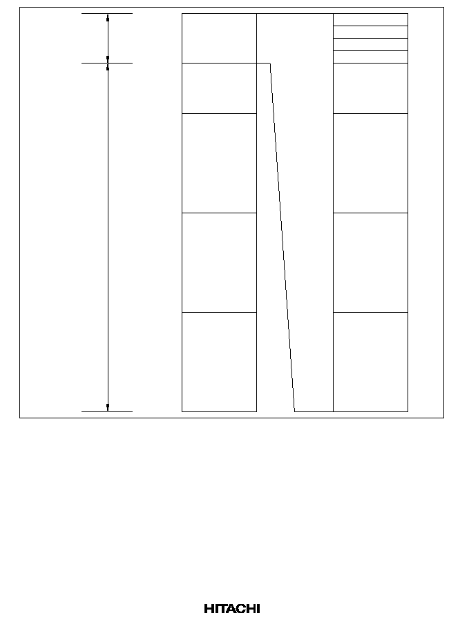
382
H'0000
H'01FF
H'0200
H'03FF
H'0400
H'07FF
H'0800
H'0BFF
H'0C00
H'0FFF
H'0000
H'0FFF
H'1000
H'1FFF
H'2000
H'3FFF
H'4000
H'5FFF
H'6000
H'7FFF
Small block
area
(4 kbytes)
Large block
area
(28 kbytes)
SB7 to SB0
4 kbytes
LB0
4 kbytes
LB1
8 kbytes
LB2
8 kbytes
LB3
8 kbytes
SB0 128 bytes
SB1 128 bytes
SB2 128 bytes
SB3 128 bytes
SB4
512 bytes
SB5
1 kbyte
SB6
1 kbyte
SB7
1 kbyte
Figure 19.2 Erase Block Map

383
Table 19.6
Erase Blocks and Corresponding Bits
Register
Bit
Block
Address
Size
EBR1
0
LB0
H'1000 to H'1FFF
4 kbytes
1
LB1
H'2000 to H'3FFF
8 kbytes
2
LB2
H'4000 to H'5FFF
8 kbytes
3
LB3
H'6000 to H'7FFF
8 kbytes
EBR2
0
SB0
H'0000 to H'007F
128 bytes
1
SB1
H'0080 to H'00FF
128 bytes
2
SB2
H'0100 to H'017F
128 bytes
3
SB3
H'0180 to H'01FF
128 bytes
4
SB4
H'0200 to H'03FF
512 bytes
5
SB5
H'0400 to H'07FF
1 kbyte
6
SB6
H'0800 to H'0BFF
1 kbyte
7
SB7
H'0C00 to H'0FFF
1 kbyte
19.3
On-Board Programming Modes
When an on-board programming mode is selected, the on-chip flash memory can be programmed,
erased, and verified. There are two on-board programming modes: boot mode, and user
programming mode. These modes are selected by inputs at the mode pins (MD
1
and MD
0
) and
FV
PP
pin. Table 19.7 indicates how to select the on-board programming modes. For details on
applying voltage V
PP
, refer to section 19.7, Flash Memory Programming and Erasing Precautions
(5).
Table 19.7
On-Board Programming Mode Selection
Mode Selections
FV
PP
MD
1
MD
0
Notes
Boot mode
Mode 2
12 V
*
12 V
*
0
0: V
IL
Mode 3
12 V
*
1
1: V
IH
User programming
Mode 2
1
0
mode
Mode 3
1
1
Note:
*
For details on the timing of 12 V application, see notes 6 to 8 in the Notes on Use of Boot
Mode at the end of this section.
In boot mode, the mode control register (MDCR) can be used to monitor the mode (mode 2
or 3) in the same way as in normal mode.
Example: Set the mode pins for mode 2 boot mode (MD
1
= 12 V, MD
0
= 0 V).
If the mode select bits of MDCR are now read, they will indicate mode 2 (MDS1 = 1, MDS0
= 0).
384
19.3.1
Boot Mode
To use boot mode, a user program for programming and erasing the flash memory must be
provided in advance on the host machine (which may be a personal computer). Serial
communication interface channel 1 is used in asynchronous mode. If the H8/3334YF is placed in
boot mode, after it comes out of reset, a built-in boot program is activated. This program starts by
measuring the low period of data transmitted from the host and setting the bit rate register (BRR)
accordingly. The H8/3334YF's built-in serial communication interface (SCI) can then be used to
download the user program from the host machine. The user program is stored in on-chip RAM.
After the program has been stored, execution branches to address H'FBE0 in the on-chip RAM,
and the program stored on RAM is executed to program and erase the flash memory. Figure 19.4
shows the boot-mode execution procedure.
HOST
Receive data to be programmed
Transmit verification data
H8/3334YF
RxD
1
TxD
1
SCI
Figure 19.3 Boot-Mode System Configuration
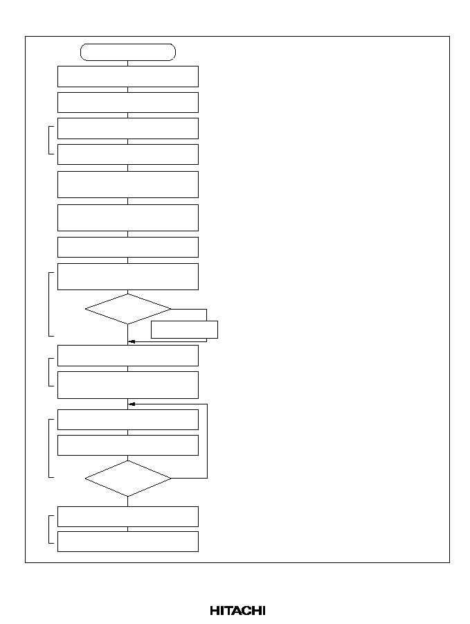
385
Boot-Mode Execution Procedure: Figure 19.4 shows the boot-mode execution procedure.
Start
Program H8/3334YF pins for boot mode,
and reset
Host transmits H'00 data continuously
at desired bit rate
H8/3334YF measures low period
of H'00 data transmitted from host
H8/3334YF computes bit rate and
sets bit rate register
After completing bit-rate alignment, H8/3334YF
sends one H'00 data byte to host to indicate
that alignment is completed
Host checks that this byte, indicating
completion of bit-rate alignment, is received
normally, then transmits one H'55 byte
After receiving H'55, H8/3334YF sends part of
the boot program to RAM
H8/3334YF transfers one user program
byte to RAM
*
2
H8/3334YF calculates number of bytes left
to be transferred (N = N ≠ 1)
All bytes transferred?
(N = 0?)
All data = H'FF?
Erase all flash
memory blocks
*
3
After transferring the user program to RAM,
H8/3334YF transmits one H'AA data byte to host
No
Yes
Yes
No
1
2
3
4
5
6
7
9
H8/3334YF branches to the RAM boot
area (H'FC00 to H'FF2F), then checks the
data in the user area of flash memory
H8/3334YF receives two bytes indicating byte
length (N) of program to be downloaded
to on-chip RAM
*
1
8
After checking that all data in flash memory is H'FF,
H8/3334YF transmits one H'AA data byte to host
H8/3334YF branches to H'FBE0 in RAM area and
executes user program downloaded into RAM
10
1. Program the H8/3334YF pins for boot mode, and start the
H8/3334YF from a reset.
2. Set the host's data format to 8 bits + 1 stop bit, select the
desired bit rate (2400, 4800, or 9600 bps), and transmit
H'00 data continuously.
3. The H8/3334YF repeatedly measures the low period of
the RxD1 pin and calculates the host's asynchronous-
communication bit rate.
4. When SCI bit-rate alignment is completed, the
H8/3334YF transmits one H'00 data byte to indicate
completion of alignment.
5. The host should receive the byte transmitted from the
H8/3334YF to indicate that bit-rate alignment is
completed, check that this byte is received normally, then
transmit one H'55 byte.
6. After receiving H'55, H8/3334YF sends part of the boot
program to H'FB80 to H'FBDF and H'FC00 to H'FF2F of
RAM.
7. After branching to the boot program area (H'FC00 to
H'FF2F) in RAM, the H8/3334YF checks whether the
flash memory already contains any programmed data. If
so, all blocks are erased.
8. After the H8/3334YF transmits one H'AA data byte, the
host transmits the byte length of the user program to be
transferred to the H8/3334YF. The byte length must be
sent as two-byte data, upper byte first and lower byte
second. After that, the host proceeds to transmit the user
program. As verification, the H8/3334YF echoes each
byte of the received byte-length data and user program
back to the host.
9. The H8/3334YF stores the received user program in on-
chip RAM in a 910-byte area from H'FBE0 to H'FF6D.
10. After transmitting one H'AA data byte, the H8/3334YF
branches to address H'FBE0 in on-chip RAM and
executes the user program stored in the area from
H'FBE0 to H'FF6D.
Notes:
*
1 The user can use 910 bytes of RAM. The number
of bytes transferred must not exceed 910 bytes.
Be sure to transmit the byte length in two bytes,
upper byte first and lower byte second. For
example, if the byte length of the program to be
transferred is 256 bytes (H'0100), transmit H'01
as the upper byte, followed by H'00 as the lower
byte.
*
2 The part of the user program that controls the
flash memory should be coded according to the
flash memory write/erase algorithms given later.
*
3 If a memory cell malfunctions and cannot be
erased, the H8/3334YF transmits one H'FF byte
to report an erase error, halts erasing, and halts
further operations.
Figure 19.4 Boot Mode Flowchart
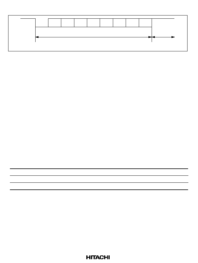
386
Automatic Alignment of SCI Bit Rate
D0
D1
D2
D3
D4
D5
D6
D7
Start
bit
Stop
bit
This low period (9 bits) is measured (H'00 data)
High for at
least 1 bit
Figure 19.5 Measurement of Low Period in Data Transmitted from Host
When started in boot mode, the H8/3334YF measures the low period in asynchronous SCI data
transmitted from the host (figure 19.5). The data format is eight data bits, one stop bit, and no
parity bit. From the measured low period (9 bits), the H8/3334YF computes the host's bit rate.
After aligning its own bit rate, the H8/3334YF sends the host 1 byte of H'00 data to indicate that
bit-rate alignment is completed. The host should check that this alignment-completed indication is
received normally and send one byte of H'55 back to the H8/3334YF. If the alignment-completed
indication is not received normally, the H8/3334YF should be reset, then restarted in boot mode to
measure the low period again. There may be some alignment error between the host's and
H8/3334YF's bit rates, depending on the host's bit rate and the H8/3334YF's system clock
frequency. To have the SCI operate normally, set the host's bit rate to 2400, 4800, or 9600 bps
*1
.
Table 19.8 lists typical host bit rates and indicates the clock-frequency ranges over which the
H8/3334YF can align its bit rate automatically. Boot mode should be used within these frequency
ranges
*2
.
Table 19.8
System Clock Frequencies Permitting Automatic Bit-Rate Alignment by
H8/3334YF
Host Bit Rate
*
1
System Clock Frequencies Permitting Automatic Bit-Rate Alignment
by H8/3334YF
9600 bps
8 MHz to 16 MHz
4800 bps
4 MHz to 16 MHz
2400 bps
2 MHz to 16 MHz
Notes:
*
1 Use a host bit rate setting of 2400, 4800, or 9600 bps only. No other setting should be
used.
*
2 Although the H8/3334YF may also perform automatic bit-rate alignment with bit rate
and system clock combinations other than those shown in table 19.8, there will be a
slight difference between the bit rates of the host and the H8/3334YF, and subsequent
transfer will not be performed normally. Therefore, only a combination of bit rate and
system clock frequency within one of the ranges shown in table 19.8 can be used for
boot mode execution.

387
RAM Area Allocation in Boot Mode: In boot mode, the 96 bytes from H'FB80 to H'FBDF and
the 18 bytes from H'FF6E to H'FF7F are reserved for use by the boot program, as shown in figure
19.6. The user program is transferred into the area from H'FBE0 to H'FF6D (910 bytes). The boot
program area can be used after the transition to execution of the user program transferred into
RAM. If a stack area is needed, set it within the user program.
User program
transfer area
(910 bytes)
Boot program
area
*
(18 bytes)
Boot program
area
*
(96 bytes)
H'FB80
H'FBE0
H'FF6E
H'FF7F
Note:
*
This area cannot be used until the H8/3334YF starts to execute the user program
transferred to RAM (until it has branched to H'FBE0 in RAM). Note that even after the
branch to the user program, the boot program area (H'FB80 to H'FBDF, H'FF6E to
H'FF7F) still contains the boot program.
Note also that 16 bytes (H'FB80 to H'FB8F) of this area cannot be used if an interrupt
handling routine is executed within the boot program. For details see section 19.4.9,
Interrupt Handling during Flash Memory Programming and Erasing.
Figure 19.6 RAM Areas in Boot Mode

388
Notes on Use of Boot Mode
1. When the H8/3334YF comes out of reset in boot mode, it measures the low period of the input
at the SCI's RxD
1
pin. The reset should end with RxD
1
high. After the reset ends, it takes about
100 states for the H8/3334YF to get ready to measure the low period of the RxD
1
input.
2. In boot mode, if any data has been programmed into the flash memory (if all data is not H'FF),
all flash memory blocks are erased. Boot mode is for use when user programming mode is
unavailable, e.g. the first time on-board programming is performed, or if the update program
activated in user programming mode is accidentally erased.
3. Interrupts cannot be used while the flash memory is being programmed or erased.
4. The RxD
1
and TxD
1
pins should be pulled up on-board.
5. Before branching to the user program (at address H'FBE0 in the RAM area), the H8/3334YF
terminates transmit and receive operations by the on-chip SCI (by clearing the RE and TE bits
of the serial control register to 0 in channel 1), but the auto-aligned bit rate remains set in bit
rate register BRR. The transmit data output pin (TxD
1
) is in the high output state (in port 8, the
bits P8
4
DDR of the port 8 data direction register and P8
4
DR of the port 8 data register are set
to 1).
At this time, the values of general registers in the CPU are undetermined. Thus these registers
should be initialized immediately after branching to the user program. Especially in the case of
the stack pointer, which is used implicitly in subroutine calls, the stack area used by the user
program should be specified.
There are no other changes to the initialized values of other registers.
6. Boot mode can be entered by starting from a reset after 12 V is applied to the MD
1
and FV
PP
pins according to the mode setting conditions listed in table 19.7. Note the following points
when turning the V
PP
power on.
When reset is released (at the rise from low to high), the H8/3334YF checks for 12-V input at
the MD
1
and FV
PP
pins. If it detects that these pins are programmed for boot mode, it saves that
status internally. The threshold point of this voltage-level check is in the range from
approximately V
CC
+ 2 V to 11.4 V, so boot mode will be entered even if the applied voltage is
insufficient for programming or erasure (11.4 V to 12.6 V). When the boot program is
executed, the V
PP
power supply must therefore be stabilized within the range of 11.4 V to
12.6 V before the branch to the RAM area occurs. See figure 19.20.
Make sure that the programming voltage V
PP
does not exceed 12.6 V during the transition to
boot mode (at the reset release timing) and does not go outside the range of 12 V ± 0.6 V while
in boot mode. Boot mode will not be executed correctly if these limits are exceeded. In

389
addition, make sure that V
PP
is not released or shut off while the boot program is executing or
the flash memory is being programmed or erased.
*1
Boot mode can be released by driving the reset pin low, waiting at least ten system clock
cycles, then releasing the application of 12 V to the MD
1
and FV
PP
pins and releasing the reset.
The settings of external pins must not change during operation in boot mode.
During boot mode, if input of 12 V to the MD
1
pin stops but no reset input occurs at the
RES
pin, the boot mode state is maintained within the chip and boot mode continues (but do not
stop applying 12 V to the FV
PP
pin during boot mode
*1
).
If a watchdog timer reset occurs during boot mode, this does not release the internal mode
state, but the internal boot program is restarted.
Therefore, to change from boot mode to another mode, the boot-mode state within the chip
must be released by a reset input at the
RES
pin before the mode transition can take place.
7. If the input level of the MD
1
pin is changed during a reset (e.g., from 0 V to 5 V then to 12 V
while the input to the
RES
pin is low), the resultant switch in the microcontroller's operating
mode will affect the bus control output signals (
AS
,
RD
, and
WR
) and the status of ports that
can be used for address output
*2
.
Therefore, either set these pins so that they do not output signals during the reset, or make sure
that their output signals do not collide with other signals outside the microcontroller.
8. When applying 12 V to the MD
1
and FV
PP
pins, make sure that peak overshoot does not exceed
the rated limit of 13 V.
Also, be sure to connect a decoupling capacitor to the FV
PP
and MD
1
pins.
Notes: *1 For details on applying, releasing, and shutting off V
PP
, see note (5) in section 19.7,
Flash Memory Programming and Erasing Precautions.
*2 These ports output low-level address signals if the mode pins are set to mode 1
during the reset. In all other modes, these ports are in the high-impedance state. The
bus control output signals are high if the mode pins are set for mode 1 or 2 during
the reset. In mode 3, they are at high impedance.

390
19.3.2
User Programming Mode
When set to user programming mode, the H8/3334YF can erase and program its flash memory by
executing a user program. On-board updates of the on-chip flash memory can be carried out by
providing on-board circuits for supplying V
PP
and data, and storing an update program in part of
the program area.
To select user programming mode, select a mode that enables the on-chip ROM (mode 2 or 3) and
apply 12 V to the FV
PP
pin, either during a reset, or after the reset has ended (been released) but
while flash memory is not being accessed. In user programming mode, the on-chip supporting
modules operate as they normally would in mode 2 or 3, except for the flash memory. However,
hardware standby mode cannot be set while 12 V is applied to the FV
PP
pin.
The flash memory cannot be read while it is being programmed or erased, so the update program
must either be stored in external memory, or transferred temporarily to the RAM area and
executed in RAM.

391
User Programming Mode Execution Procedure (Example)*: Figure 19.7 shows the execution
procedure for user programming mode when the on-board update routine is executed in RAM.
Note: * Do not apply 12 V to the FV
PP
pin during normal operation. To prevent flash memory
from being accidentally programmed or erased due to program runaway etc., apply 12 V
to FV
PP
only when programming or erasing flash memory. Overprogramming or
overerasing due to program runaway can cause memory cells to malfunction. While 12 V
is applied, the watchdog timer should be running and enabled to halt runaway program
execution, so that program runaway will not lead to overprogramming or overerasing. For
details on applying, releasing, and shutting off V
PP
, see section 19.7, Flash Memory
Programming and Erasing Precautions (5).
Set MD
1
and MD
0
to 10 or 11
(apply V
IH
to V
CC
to MD
1
)
Start from reset
Branch to flash memory on-board
update routine in RAM
FV
PP
= 12 V
(user programming mode)
Execute flash memory
on-board update routine in RAM
(update flash memory)
1
2
3
4
5
Branch to flash memory
on-board update program
Transfer on-board update routine
into RAM
6
7
8
Release FV
PP
(exit user programming mode)
Branch to application program
in flash memory
*
Procedure
The flash memory on-board update
program is written in flash memory ahead
of time by the user.
1. Set MD1 and MD0 of the H8/3334YF
to 10 or 11, and start from a reset.
2. Branch to the flash memory on-board
update program in flash memory.
3. Transfer the on-board update routine
into RAM.
4. Branch to the on-board update routine
that was transferred into RAM.
5. Apply 12 V to the FV
PP
pin, to enter
user programming mode.
6. Execute the flash memory on-board
update routine in RAM, to perform an
on-board update of the flash memory.
7. Change the voltage at the FV
PP
pin
from 12 V to V
CC
, to exit user
programming mode.
8. After the on-board update of flash
memory ends, execution branches to
an application program in flash
memory.
Note:
*
After the update is finished, when input of 12 V to the FV
PP
pin is released, the flash
memory read setup time (t
FRS
) must elapse before any program in flash memory is
executed. This is the required setup time from when the FV
PP
pin reaches the (V
CC
+
2 V) level after 12 V is released until flash memory can be read.
Figure 19.7 User Programming Mode Operation (Example)

392
19.4
Programming and Erasing Flash Memory
The H8/3334YF's on-chip flash memory is programmed and erased by software, using the CPU.
The flash memory can operate in program mode, erase mode, program-verify mode, erase-verify
mode, or prewrite-verify mode. Transitions to these modes can be made by setting the P, E, PV,
and EV bits in the flash memory control register (FLMCR).
The flash memory cannot be read while being programmed or erased. The program that controls
the programming and erasing of the flash memory must be stored and executed in on-chip RAM or
in external memory. A description of each mode is given below, with recommended flowcharts
and sample programs for programming and erasing.
For details on programming and erasing, refer to section 19.7, Flash Memory Programming and
Erasing Precautions.
19.4.1
Program Mode
To write data into the flash memory, follow the programming algorithm shown in figure 19.8. This
programming algorithm can write data without subjecting the device to voltage stress or impairing
the reliability of programmed data.
To program data, first specify the area to be written in flash memory with erase block registers
EBR1 and EBR2, then write the data to the address to be programmed, as in writing to RAM. The
flash memory latches the address and data in an address latch and data latch. Next set the P bit in
FLMCR, selecting program mode. The programming duration is the time during which the P bit is
set. A software timer should be used to provide a programming duration of about 10 to 20 µs. The
value of N, the number of attempts, should be set so that the total programming time does not
exceed 1 ms. Programming for too long a time, due to program runaway for example, can cause
device damage. Before selecting program mode, set up the watchdog timer so as to prevent
overprogramming.

393
19.4.2
Program-Verify Mode
In program-verify mode, after data has been programmed in program mode, the data is read to
check that it has been programmed correctly.
After the programming time has elapsed, exit programming mode (clear the P bit to 0) and select
program-verify mode (set the PV bit to 1). In program-verify mode, a program-verify voltage is
applied to the memory cells at the latched address. If the flash memory is read in this state, the
data at the latched address will be read. After selecting program-verify mode, wait 4 µs or more
before reading, then compare the programmed data with the verify data. If they agree, exit
program-verify mode and program the next address. If they do not agree, select program mode
again and repeat the same program and program-verify sequence. Do not repeat the program and
program-verify sequence more than 50 times* for the same bit.
Note: * Keep the total programming time under 1 ms for each bit.

394
19.4.3
Programming Flowchart and Sample Program
Flowchart for Programming One Byte
Start
n = 1
Enable watchdog timer
*
2
Select program mode
(P bit = 1 in FLMCR)
Wait (x)
µ
s
*
4
Clear P bit
Disable watchdog timer
Select program-verify mode
(PV bit = 1 in FLMCR)
Wait (t
VS
1)
µ
s
*
4
Verify
*
3
(read memory)
No go
OK
Clear PV bit
End (1-byte data programmed)
End of programming
Clear PV bit
Programming error
n
N?
*
4
n + 1
n
No
End of verification
Write data to flash memory (flash
memory latches write
address and data)
*
1
Set erase block register
(set bit of block to be programmed to 1)
Yes
Clear erase block register
(clear bit of programmed block to 0)
Notes:
*
1 Write the data to be programmed
with a byte transfer instruction.
*
2 Set the timer overflow interval to the
shortest value (CKS2, CKS1, CKS0
all cleared to 0).
*
3 Read the memory data to be verified
with a byte transfer instruction.
*
4 x:
10 to 20
µ
s
t
VS
1: 4
µ
s or more
N:
50 (set N so that total
programming time does not
exceed 1 ms)
Figure 19.8 Programming Flowchart

395
Sample Program for Programming One Byte: This program uses the following registers.
R0H: Specifies blocks to be erased.
R1H: Stores data to be programmed.
R1L: Stores data to be read.
R3:
Stores address to be programmed. Valid addresses are H'0000 to H'7FFF.
R4:
Sets program and program-verify timing loop counters, and also stores register setting
value.
R5:
Sets program timing loop counter.
R6L: Used for program-verify fail count.
Arbitrary data can be programmed at an arbitrary address by setting the address in R3 and the data
in R1H.
The setting of #a and #b values depends on the clock frequency. Set #a and #b values according to
tables 19.9 (1) and (2).
FLMCR: .EQU H'FF80
EBR1: .EQU H'FF82
EBR2: .EQU H'FF83
TCSR: .EQU H'FFA8
.ALIGN 2
PRGM: MOV.B #H'**, R0H
;
MOV.B R0H, @EBR*:8
; Set EBR
*
MOV.B #H'00, R6L
; Program-verify fail counter
MOV.W #H'a, R5
; Set program loop counter
MOV.B R1H, @R3
; Dummy write
PRGMS: INC R6L
; Program-verify fail counter + 1
R6L
MOV.W #H'A578, R4
;
MOV.W R4, @TCSR
; Start watchdog timer
MOV.W R5, R4
; Set program loop counter
BSET #0, @FLMCR:8
; Set P bit
LOOP1: SUBS #1, R4
;
MOV.W R4, R4
;
BNE LOOP1
; Wait loop
BCLR #0, @FLMCR:8
; Clear P bit
MOV.W #H'A500, R4
;
MOV.W R4, @TCSR
; Stop watchdog timer
MOV.B #H'b , R4H
; Set program-verify loop counter
BSET #2, @FLMCR:8
; Set PV bit
LOOP2: DEC R4H
;
BNE LOOP2
; Wait loop
MOV.B @R3, R1L
; Read programmed address
CMP.B R1H, R1L
; Compare programmed data with read data
BEQ PVOK
; Program-verify decision
BCLR #2, @FLMCR:8
; Clear PV bit

396
CMP.B #H'32, R6L
; Program-verify executed 50 times?
BEQ NGEND
; If program-verify executed 50 times, branch to NGEND
BRA PRGMS
; Program again
PVOK: BCLR #2, @FLMCR:8
; Clear PV bit
MOV.B #H'00, R6L
;
MOV.B R6L, @EBR*:8
; Clear EBR
*
One byte programmed
NGEND:
Programming error
19.4.4
Erase Mode
To erase the flash memory, follow the erasing algorithm shown in figure 19.11. This erasing
algorithm can erase data without subjecting the device to voltage stress or impairing the reliability
of programmed data.
To erase flash memory, before starting to erase, first place all memory data in all blocks to be
erased in the programmed state (program all memory data to H'00). If all memory data is not in the
programmed state, follow the sequence described later (figure 18-17) to program the memory data
to zero. Select the flash memory areas to be erased with erase block registers 1 and 2 (EBR1 and
EBR2). Next set the E bit in FLMCR, selecting erase mode. The erase time is the time during
which the E bit is set. To prevent overerasing, use a software timer to divide the erase time into
repeated 10 ms intervals, and perform erase operations a maximum of 3000 times so that the total
erase time does not exceed 30 seconds. Overerasing, due to program runaway for example, can
give memory cells a negative threshold voltage and cause them to operate incorrectly. Before
selecting erase mode, set up the watchdog timer so as to prevent overerasing.
19.4.5
Erase-Verify Mode
In erase-verify mode, after data has been erased, it is read to check that it has been erased
correctly. After the erase time has elapsed, exit erase mode (clear the E bit to 0) and select erase-
verify mode (set the EV bit to 1). Before reading data in erase-verify mode, write H'FF dummy
data to the address to be read. This dummy write applies an erase-verify voltage to the memory
cells at the latched address. If the flash memory is read in this state, the data at the latched address
will be read. After the dummy write, wait 2 µs or more before reading. When performing the
initial dummy write, wait 4 µs or more after selecting erase-verify mode. If the read data has been
successfully erased, perform an erase-verify (dummy write, wait 2 µs or more, then read) for the
next address. If the read data has not been erased, select erase mode again and repeat the same
erase and erase-verify sequence through the last address. Do not repeat the erase and erase-verify
sequence more than 3000 times, however.
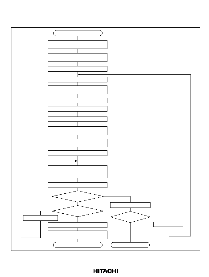
397
19.4.6
Erasing Flowchart and Sample Program
Flowchart for Erasing One Block
Start
Write 0 data in all addresses
to be erased (prewrite)
*
1
n = 1
Set erase block register
(set bit of block to be erased to 1)
Enable watchdog timer
*
2
Select erase mode
(E bit = 1 in FLMCR)
Wait (x) ms
*
5
Clear E bit
Disable watchdog timer
Set top address in block
as verify address
Select erase-verify mode
(EV bit = 1 in FLMCR)
Wait (t
VS
1)
µ
s
*
5
Dummy write to verify address
*
3
(flash memory latches address)
Verify
*
4
(read data H'FF?)
Last address?
Address + 1
address
Yes
OK
No go
No
Yes
Clear EV bit
Clear erase block register
(clear bit of erased block to 0)
End of block erase
Clear EV bit
Erase error
n
N?
*
5
Erase-verify ends
Erasing ends
n + 1
n
No
Wait (t
VS
2)
µ
s
*
5
Notes:
*
1 Program all addresses to be
erased by following the prewrite
flowchart.
*
2 Set the watchdog timer overflow
interval to the value indicated in
table 19.10.
*
3 For the erase-verify dummy write,
write H'FF with a byte transfer
instruction.
*
4 Read the data to be verified with
a byte transfer instruction. When
erasing two or more blocks, clear
the bits of erased blocks in the
erase block registers, so that only
unerased blocks will be erased
again.
*
5 x:
10 ms
t
VS
1: 4
µ
s or more
t
VS
2: 2
µ
s or more
N:
3000
Figure 19.9 Erasing Flowchart
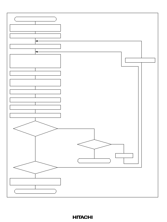
398
Prewrite Flowchart
End of prewrite
n
N?
*
4
n + 1
n
No
Start
Set start address
*
5
Write H'00 to flash memory
(Flash memory latches
write address and write data)
*
1
Enable watchdog timer
*
2
Select program mode
( P bit = 1 in FLMCR)
Wait (x)
µ
s
*
4
Disable watchdog timer
Wait (t
VS
1)
µ
s
*
4
Prewrite verify
*
3
(read data = H'00?)
No go
No
Yes
Clear P bit
End of
programming
Programming error
Address + 1
address
OK
Yes
Set erase block register
(set bit of block to be programmed to 1)
Clear erase block register
(clear bit of programmed block to 0)
n = 1
Last address?
*
5
Notes:
*
1 Use a byte transfer instruction.
*
2 Set the timer overflow interval to the
shortest value (CKS2, CKS1, CKS0
all cleared to 0).
*
3 In prewrite-verify mode P, E, PV,
and EV are all cleared to 0 and 12 V
is applied to FV
PP
. Read the data
with a byte transfer instruction.
*
4 x:
10 to 20
µ
s
t
VS
1: 4
µ
s or more
N:
50 (set N so that total
programming time does not
exceed 1 ms)
*
5 Start and last addresses are top and
last addresses of the block to be
erased.
Figure 19.10 Prewrite Flowchart

399
Sample Block-Erase Program: This program uses the following registers.
R0:
Specifies block to be erased, and also stores address used in prewrite and erase-verify.
R1H: Stores data to be read, and also used for dummy write.
R2:
Stores last address of block to be erased.
R3:
Stores address used in prewrite and erase-verify.
R4:
Sets timing loop counters for prewrite, prewrite-verify, erase, and erase-verify, and also
stores register setting value.
R5:
Sets prewrite and erase timing loop counters.
R6L: Used for prewrite-verify and erase-verify fail count.
The setting of #a, #b, #c, #d, and #e values in the program depends on the clock frequency. Set #a,
#b, #c, #d, and #e values according tables 19.9 (1) and (2), and 19.10 Erase block registers (EBR1
and EBR2) should be set according to sections 19.2.2 and 19.2.3. #BLKSTR and #BLKEND are
the top and last addresses of the block to be erased. Set #BLKSTR and #BLKEND according to
figure 19.2.

400
FLMCR: .EQU H'FF80
EBR1: .EQU H'FF82
EBR2: .EQU H'FF83
TCSR: .EQU H'FFA8
.ALIGN 2
MOV.B #H'**, ROH
;
MOV.B ROH, @EBR*:8
; Set EBR*
; #BLKSTR is top address of block to be erased.
; #BLKEND is last address of block to be erased.
MOV.W #BLKSTR, R0
; Top address of block to be erased
MOV.W #BLKEND, R2
; Last address of block to be erased
ADDS #1, R2
; Last address of block to be erased + 1
R2
; Execute prewrite
MOV.W R0, R3
; Top address of block to be erased
PREWRT: MOV.B #H'00, R6L
; Prewrite-verify fail counter
MOV.W #H'a, R5
; Set prewrite loop counter
PREWRS: INC R6L
; Prewrite-verify fail counter + 1
R6L
MOV.B #H'00 R1H
;
MOV.B R1H, @R3
; Write H'00
MOV.W #H'A578, R4
;
MOV.W R4, @TCSR
; Start watchdog timer
MOV.W R5, R4
; Set prewrite loop counter
BSET #0, @FLMCR:8
; Set P bit
LOOPR1: SUBS #1, R4
;
MOV.W R4, R4
;
BNE LOOPR1
; Wait loop
BCLR #0, @FLMCR:8
; Clear P bit
MOV.W #H'A500, R4
;
MOV.W R4, @TCSR
; Stop watchdog timer
MOV.B #H'c, R4H
; Set prewrite-verify loop counter
LOOPR2: DEC R4H
;
BNE LOOPR2
; Wait loop
MOV.B @R3, R1H
; Read data = H'00?
BEQ PWVFOK
; If read data = H'00 branch to PWVFOK
CMP.B #H'32, R6L
; Prewrite-verify executed 50 times?
BEQ ABEND1
; If prewrite-verify executed 50 times, branch to ABEND1
BRA PREWRS
; Prewrite again
ABEND1:
Programming error
PWVFOK: ADDS #1, R3
; Address + 1
R3
CMP.W R2, R3
; Last address?
BNE PREWRT
; If not last address, prewrite next address

401
;
Execute erase
ERASES: MOV.W #H'0000, R6
; Erase-verify fail counter
MOV.W #H'd, R5
; Set erase loop count
ERASE: ADDS #1, R6
; Erase-verify fail counter + 1
R6
MOV.W #H'e, R4
;
MOV.W R4, @TCSR
; Start watchdog timer
MOV.W R5, R4
; Set erase loop counter
BSET #1, @FLMCR:8
; Set E bit
LOOPE: NOP
NOP
NOP
NOP
SUBS #1, R4
;
MOV.W R4, R4
;
BNE LOOPE
; Wait loop
BCLR #1, @FLMCR:8
; Clear E bit
MOV.W #H'A500, R4
;
MOV.W R4, @TCSR
; Stop watchdog timer
; Execute erase-verify
MOV.W R0, R3
; Top address of block to be erased
MOV.B #H'b, R4H
; Set erase-verify loop counter
BSET #3, @FLMCR:8
; Set EV bit
LOOPEV: DEC R4H
;
BNE LOOPEV
; Wait loop
EVR2: MOV.B #H'FF, R1H
;
MOV.B R1H, @R3
; Dummy write
MOV.B #H'c, R4H
; Set erase-verify loop counter
LOOPDW: DEC R4H
;
BNE LOOPDW
; Wait loop
MOV.B @R3+, R1H
; Read
CMP.B #H'FF, R1H
; Read data = H'FF?
BNE RERASE
; If read data
H'FF, branch to RERASE
CMP.W R2, R3
; Last address of block?
BNE EVR2
BRA OKEND
RERASE: BCLR #3, @FLMCR:8
; Clear EV bit
SUBS #1, R3
; Erase-verify address ≠ 1
R3
BRER: MOV.W #H'0BB8, R4
;
CMP.W R4, R6
; Erase-verify executed 3000 times?
BNE ERASE
; If erase-verify not executed 3000 times, erase again
BRA ABEND2
; If erase-verify executed 3000 times, branch to ABEND2
OKEND: BCLR #3, @FLMCR:8
; Clear EV bit
MOV.B #H'00, R6L
;
MOV.B R6L, @EBR*:8
; Clear EBR*
One block erased
ABEND2:
Erase error
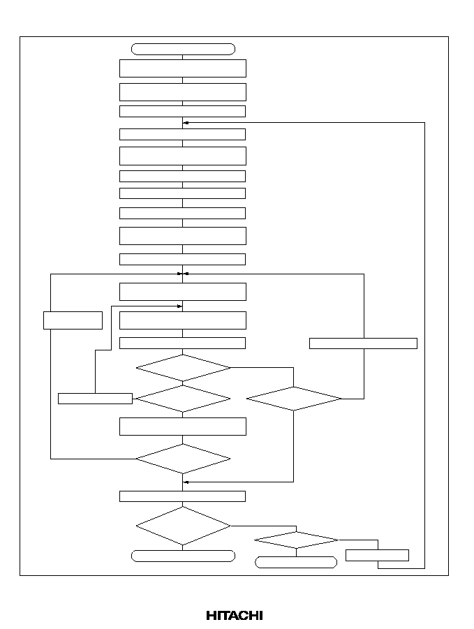
402
Flowchart for Erasing Multiple Blocks
Start
Write 0 data to all addresses to be
erased (prewrite)
*
1
n = 1
Set erase block registers
(set bits of blocks to be erased to 1)
Enable watchdog timer
*
2
Select erase mode (E bit = 1 in FLMCR)
Wait (X) ms
*
5
Clear E bit
Disable watchdog timer
Select erase-verify mode
(EV bit = 1 in FLMCR)
Wait (t
VS
1)
µ
s
*
5
Set top address of block as
verify address
Dummy write to verify address
*
3
(flash memory latches address)
Erase-verify
next block
Verify
*
4
(read data H'FF?)
Last address
in block?
Address + 1
address
Clear EBR bit of erased block
All erased blocks
verified?
Clear EV bit
All blocks erased?
(EBR1 = EBR2 = 0?)
End of erase
n
N?
*
5
Erase error
n + 1
n
No
Yes
No
No
Yes
No
Yes
No go
OK
Erasing ends
All erased blocks
verified?
Erase-verify next block
Yes
No
Yes
Wait (t
VS
2)
µ
s
*
5
Notes:
*
1 Program all addresses to be
erased by following the
prewrite flowchart.
*
2 Set the watchdog timer
overflow interval to the value
indicated in table 19.10.
*
3 For the erase-verify dummy
write, write H'FF with a byte
transfer instruction.
*
4 Read the data to be verified
with a byte transfer instruction.
When erasing two or more
blocks, clear the bits of erased
blocks in the erase block
register, so that only unerased
blocks will be erased again.
*
5 X:
10 ms
t
VS
1: 4
µ
s or more
t
VS
2: 2
µ
s or more
N:
3000
Figure 19.11 Multiple-Block Erase Flowchart

403
Sample Multiple-Block Erase Program: This program uses the following registers.
R0:
Specifies blocks to be erased (set as explained below), and also stores address used in
prewrite and erase-verify.
R1H: Used to test bits 8 to 11 of R0 stores register read data, and also used for dummy write.
R1L: Used to test bits 0 to 11 of R0.
R2:
Specifies address where address used in prewrite and erase-verify is stored.
R3:
Stores address used in prewrite and erase-verify.
R4:
Stores last address of block to be erased.
R5:
Sets prewrite and erase timing loop counters.
R6L: Used for prewrite-verify and erase-verify fail count.
Arbitrary blocks can be erased by setting bits in R0. Write R0 with a word transfer instruction.
A bit map of R0 and a sample setting for erasing specific blocks are shown next.
Bit
15
14
13
12
11
10
9
8
7
6
5
4
3
2
1
0
R0
--
--
--
--
LB3 LB2 LB1 LB0 SB7 SB6 SB5 SB4 SB3 SB2 SB1 SB0
Corresponds to EBR1
Corresponds to EBR2
Note:
Clear bits 15, 14, 13, and 12 to 0.
Example: to erase blocks LB2, SB7, and SB0
Bit
15
14
13
12
11
10
9
8
7
6
5
4
3
2
1
0
R0
--
--
--
--
LB3 LB2 LB1 LB0 SB7 SB6 SB5 SB4 SB3 SB2 SB1 SB0
Corresponds to EBR1
Corresponds to EBR2
Setting
0
0
0
0
0
1
0
0
1
0
0
0
0
0
0
1
R0 is set as follows:
MOV.W #H'0481,R0
MOV.W R0, @EBR1
The setting of #a, #b, #c, #d, and #e values in the program depends on the clock frequency. Set #a,
#b, #c, #d, and #e values according to tables 19.9 (1), (2), and 19.10.

404
Notes: 1. In this sample program, the stack pointer (SP) is set at address FF80. As the stack area,
on-chip RAM addresses FF7E and FF7F are used. Therefore, when executing this
sample program, addresses FF7E and FF7F should not be used. In addition, the on-chip
RAM should not be disabled.
2. In this sample program, the program written in a ROM area (including external space)
is transferred into the RAM area and executed in the RAM to which the program is
transferred. #RAMSTR in the program is the starting destination address in RAM to
which the program is transferred. #RAMSTR must be set to an even number.
3. When executing this sample program in the on-chip ROM area or external space,
#RAMSTR should be set to #START.
FLMCR: .RQU H'FF80
EBR1: .EQU H'FF82
EBR2: .EQU H'FF83
TCSR: .EQU H'FFA8
STACK: .EQU H'FF80
.ALIGN2
START: MOV.W #STACK, SP
; Set stack pointer
; Set the bits in R0 following the description on the previous page. This program is a sample program to
; erase all blocks.
MOV.W #H'0FFF, R0
; Select blocks to be erased (R0: EBR1/EBR2)
MOV.W R0, @EBR1
; Set EBR1/EBR2
; #RAMSTR is starting destination address to which program is transferred in RAM.
; Set #RAMSTR to even number.
MOV.W #RAMSTR, R2
; Starting transfer destination address (RAM)
MOV.W #ERVADR, R3
;
ADD.W R3, R2
; #RAMSTR + #ERVADR
R2
MOV.W #START, R3
;
SUB.W R3, R2
; Address of data area used in RAM
MOV.B #H'00, R1L
: Used to test R1L bit in R0
PRETST: CMP.B #H'0C, R1L
; R1L = H'0C?
BEQ ERASES
; If finished checking all R0 bits, branch to ERASES
CMP.B #H'08, R1L
;
BMI EBR2PW
; Test EBR1 if R1L
8, or EBR2 if R1L < 8
MOV.B R1L, R1H
;
SUBX #H'08, R1H
; R1L ≠ 8
R1H
BTST R1H, R0H
; Test R1H bit in EBR1 (R0H)
BNE PREWRT
; If R1H bit in EBR1 (R0H) is 1, branch to PREWRT
BRA PWADD1
; If R1H bit in EBR1 (R0H) is 0, branch to PWADD1
EBR2PW: BTST R1L, R0L
; Test R1L bit in EBR2 (R0L)
BNE PREWRT
; If R1L bit in EBR2 (R0H) is 1, branch to PREWRT
PWADD1: INC R1L
; R1L + 1
R1L
MOV.W @R2+, R3
; Dummy-increment R2
BRA PRETST
;

405
; Execute prewrite
PREWRT: MOV.W @R2+, R3
; Prewrite starting address
PREW: MOV.B #H'00, R6L
; Prewrite-verify fail counter
MOV.W #H'a, R5
; Prewrite-verify loop counter
PREWRS: INC R6L
; Prewrite-verify fail counter + 1
R6L
MOV.B #H'00, R1H
;
MOV.B R1H, @R3
; Write H'00
MOV.W #H'A578, R4
;
MOV.W R4, @TCSR
; Start watchdog timer
MOV.W R5, R4
; Set prewrite loop counter
BSET #0, @FLMCR:8
; Set P bit
LOOPR1: SUBS #1, R4
;
MOV.W R4, R4
;
BNE LOOPR1
; Wait loop
BCLR #0, @FLMCR:8
; Clear P bit
MOV.W #H'A500, R4
;
MOV.W R4, @TCSR
; Stop watchdog timer
MOV.B #H'c, R4H
; Set prewrite-verify loop counter
LOOPR2: DEC R4H
;
BNE LOOPR2
; Wait loop
MOV.B @R3, R1H
; Read data = H'00?
BEQ PWVFOK
; If read data = H'00 branch to PWVFOK
CMP.B #H'32, R6L
; Prewrite-verify executed 50 times?
BEQ ABEND1
; If prewrite-verify executed 50 times, branch to ABEND1
BRA PREWRS
; Prewrite again
ABEND1:
Programming error
PWVFOK: ADDS #1, R3
; Address + 1
R3
MOV.W @R2, R4
; Top address of next block
CMP.W R4, R3
; Last address?
BNE PREW
; If not last address, prewrite next address
PWADD2: INC R1L
; Used to test R1L+1 bit in R0
BRA PRETST
; Branch to PRETST
; Execute erase
ERASES: MOV.W #H'0000, R6
; Erase-verify fail counter
MOV.W #H'd, R5
; Set erase loop count
ERASE: ADDS #1, R6
; Erase-verify fail counter + 1
R6
MOV.W #H'e, R4
;
MOV.W R4, @TCSR
; Start watchdog timer
MOV.W R5, R4
; Set erase loop counter
BSET #1, @FLMCR:8
; Set E bit
LOOPE: NOP
NOP
NOP
NOP
SUBS #1, R4
;
MOV.W R4, R4
;
BNE LOOPE
; Wait loop
BCLR #1, @FLMCR:8
; Clear E bit
MOV.W #H'A500, R4
;
MOV.W R4, @TCSR
; Stop watchdog timer

406
; Execute erase-verify
EVR: MOV.W #RAMSTR, R2
; Starting transfer destination address (RAM)
MOV.W #ERVADR, R3
;
ADD.W R3, R2
; #RAMSTR + #ERVADR
R2
MOV.W #START, R3
;
SUB.W R3, R2
; Address of data area used in RAM
MOV.B #H'00, R1L
; Used to test R1L bit in R0
MOV.B #H'b, R4H
; Set erase-verify loop counter
BSET #3, @FLMCR:8
; Set EV bit
LOOPEV: DEC R4H
;
BNE LOOPEV
; Wait loop
EBRTST: CMP.B #H'0C, R1L
; R1L = H'0C?
BEQ HANTEI
; If finished checking all R0 bits, branch to HANTEI
CMP.B #H'08, R1L
;
BMI EBR2EV
; Test EBR1 if R1L
8, or EBR2 if R1L < 8
MOV.B R1L, R1H
;
SUBX #H'08, R1H
; R1L ≠ 8
R1H
BTST R1H, R0H
; Test R1H bit in EBR1 (R0H)
BNE ERSEVF
; If R1H bit in EBR1 (R0H) is 1, branch to ERSEVF
BRA ADD01
; If R1H bit in EBR1 (R0H) is 0, branch to ADD01
EBR2EV: BTST R1L, R0L
; Test R1L bit in EBR2 (R0L)
BNE ERSEVF
; If R1L bit in EBR2 (R0H) is 1, branch to ERSEVF
ADD01: INC R1L
; R1L + 1
R1L
MOV.W @R2+, R3
; Dummy-increment R2
BRA EBRTST
;
ERASE1: BRA ERASE
; Branch to ERASE via Erase 1
ERSEVF: MOV.W @R2+, R3
; Top address of block to be erase-verified
EVR2: MOV.B #H'FF, R1H
;
MOV.B R1H, @R3
; Dummy write
MOV.B #H'c, R4H
; Set erase-verify loop counter
LOOPEP: DEC R4H
;
BNE LOOPEP
; Wait loop
MOV.B @R3+, R1H
; Read
CMP.B #H'FF, R1H
; Read data = H'FF?
BNE BLKAD
; If read data
H'FF branch to BLKAD
MOV.W @R2, R4
; Top address of next block
CMP.W R4, R3
; Last address of block?
BNE EVR2
CMP.B #H'08, R1L
BMI SBCLR
; Test EBR1 if R1L
8, or EBR2 if R1L < 8
MOV.B R1L, R1H
;
SUBX #H'08, R1H
; R1L ≠ 8
R1H
BCLR R1H, R0H
; Clear R1H bit in EBR1 (R0H)
BRA BLKAD
SBCLR: BCLR R1L, R0L
; Clear R1L bit in EBR2 (R0L)
BLKAD: INC R1L
; R1L + 1
R1L
BRA EBRTST
;
HANTEI: BCLR #3, @FLMCR:8
; Clear EV bit
MOV.W R0, @EBR1
;
BEQ EOWARI
; If EBR1/EBR2 is all 0, erasing ended normally

407
BRER: MOV.W #H'0BB8, R4
;
CMP.W R4, R6
; Erase-verify executed 3000 times?
BNE ERASE1
; If erase-verify not executed 3000 times, erase again
BRA ABEND2
; If erase-verify executed 3000 times, branch to ABEND2
;------< Block address table used in erase-verify> ------
.ALIGN 2
ERVADR: .DATA.W H'0000
; SB0
.DATA.W H'0080
; SB1
.DATA.W H'0100
; SB2
.DATA.W H'0180
; SB3
.DATA.W H'0200
; SB4
.DATA.W H'0400
; SB5
.DATA.W H'0800
; SB6
.DATA.W H'0C00
; SB7
.DATA.W H'1000
; LB0
.DATA.W H'2000
; LB1
.DATA.W H'4000
; LB2
.DATA.W H'6000
; LB3
.DATA.W H'8000
; FLASH END
EOWARI:
Erase end
ABEND2:
Erase error
Loop Counter Values in Programs and Watchdog Timer Overflow Interval Settings:
The setting of #a, #b, #c, #d, and #e values in the programs depends on the clock frequency.
Tables 19.9 (1) and (2) indicate sample loop counter settings for typical clock frequencies.
However, #e is set according to table 19.10.
As a software loop is used, calculated values including percent errors may not be the same as
actual values. Therefore, the values are set so that the total programming time and total erase time
do not exceed 1 ms and 30 s, respectively.
The maximum number of writes in the program, N, is set to 50.
Programming and erasing in accordance with the flowcharts is achieved by setting #a, #b, #c, and
#d in the programs as shown in tables 19.9 (1) and (2). #e should be set as shown in table 19.10.
Wait state insertion is inhibited in these programs. If wait states are to be used, the setting should
be made after the program ends. The setting value for the watchdog timer (WDT) overflow time is
calculated based on the number of instructions between starting and stopping of the WDT,
including the write time and erase time. Therefore, no other instructions should be added between
starting and stopping of the WDT in this program example.

408
Table 19.9 (1) #a, #b, #c, and #d Setting Values for Typical Clock Frequencies with
Program Running in the On-Chip Memory (RAM)
Clock Frequency
f = 16 MHz
f = 10 MHz
f = 8 MHz
f = 2 MHz
Variable
Time
Setting
Counter
Setting Value
Counter
Setting Value
Counter
Setting Value
Counter
Setting Value
a
(f)
Programming time
20 µs
H'0028
H'0019
H'0014
H'0005
b
(f)
tvs1
4 µs
H'0B
H'07
H'06
H'02
c
(f)
tvs2
2 µs
H'06
H'04
H'03
H'01
d
(f)
Erase time
10 ms
H'2710
H'186A
H'1388
H'04E2
Table 19.9 (2) #a, #b, #c, and #d Setting Values for Typical Clock Frequencies with
Program Running in the External Device
Clock Frequency
f = 16 MHz
f = 10 MHz
f = 8 MHz
f = 2 MHz
Variable
Time
Setting
Counter
Setting Value
Counter
Setting Value
Counter
Setting Value
Counter
Setting Value
a
(f)
Programming time
20 µs
H'000D
H'0008
H'0006
H'0001
b
(f)
tvs1
4 µs
H'04
H'03
H'02
H'01
c
(f)
tvs2
2 µs
H'02
H'02
H'01
H'01
d
(f)
Erase time
10 ms
H'0D05
H'0823
H'0682
H'01A0

409
Formula: When using a clock frequency not shown in tables 19.9 (1) and (2), follow the formula
below. The calculation is based on a clock frequency of 10 MHz.
After calculating a(f) and d(f) in the decimal system, omit the first decimal figures, and convert
them to the hexadecimal system, so that a(f) and d(f) are set to 20 µs or less and 10 ms or less,
respectively.
After calculating b(f) and c(f) in the decimal system, raise the first decimal figures, and convert
them to the hexadecimal system, so that b(f) and c(f) are set to 4 µs or more and 2 µs or more,
respectively.
Clock frequency f [MHz]
10
a (f) to d (f) =
◊
a (f = 10) to d (f = 10)
Examples for a program running in on-chip memory (RAM) at a clock frequency of 12 MHz:
a (f) =
◊
25
=
30
30
= H'001E
b (f) =
◊
7
=
8.4
9
= H'09
c (f) =
◊
4
=
4.8
5
= H'05
d (f) =
◊
6250 = 7500
7500 = H'1D4C
12
10
12
10
12
10
12
10
Table 19.10
Watchdog Timer Overflow Interval Settings
(#e Setting Value According to Clock Frequency)
Variable
Clock Frequency [MHz]
e (f)
10 MHz
frequency
16 MHz
H'A57F
2 MHz
frequency < 10 MHz
H'A57E

410
19.4.7
Prewrite Verify Mode
Prewrite-verify mode is a verify mode used when programming all bits to equalize their threshold
voltages before erasing them.
Program all flash memory to H'00 by writing H'00 using the prewrite algorithm shown in figure
19.10. H'00 should also be written when using RAM for flash memory emulation (when
prewriting a RAM area). (This also applies when using RAM to emulate flash memory erasing
with an emulator or other support tool.) After the necessary programming time has elapsed, exit
program mode (by clearing the P bit to 0) and select prewrite-verify mode (leave the P, E, PV, and
EV bits all cleared to 0). In prewrite-verify mode, a prewrite-verify voltage is applied to the
memory cells at the read address. If the flash memory is read in this state, the data at the read
address will be read. After selecting prewrite-verify mode, wait 4 µs or more before reading.
Note:
For a sample prewriting program, see the prewrite subroutine in the sample erasing
program.
19.4.8
Protect Modes
Flash memory can be protected from programming and erasing by software or hardware methods.
These two protection modes are described below.
Software Protection: Prevents transitions to program mode and erase mode even if the P or E bit
is set in the flash memory control register (FLMCR). Details are as follows.
Function
Protection
Description
Program
Erase
Verify
*
1
Block
protect
Individual blocks can be protected from erasing
and programming by the erase block registers
(EBR1 and EBR2). If H'F0 is set in EBR1 and
H'00 in EBR2, all blocks are protected from
erasing and programming.
Disabled
Disabled
Enabled
Emulation
protect
*
2
When the RAMS or RAM0 bit, but not both,
is set in the wait-state control register (WSCR),
all blocks are protected from programming and
erasing.
Disabled
Disabled
*
3
Enabled
Notes:
*
1 Three modes: program-verify, erase-verify, and prewrite-verify.
*
2 Except in RAM areas overlapped onto flash memory.
*
3 All blocks are erase-disabled. It is not possible to specify individual blocks.

411
Hardware Protection: Suspends or disables the programming and erasing of flash memory, and
resets the flash memory control register (FLMCR) and erase block registers (EBR1 and EBR2).
Details of hardware protection are as follows.
Function
Protection
Description
Program
Erase
Verify
*
1
Programing
voltage (V
PP
)
protect
When 12 V is not applied to the FV
PP
pin,
FLMCR, EBR1, and EBR2 are initialized,
disabling programming and erasing. To obtain
this protection, V
PP
should not exceed V
CC
.
*
3
Disabled
Disabled
*
2
Disabled
Reset and
standby
protect
When a reset occurs (including a watchdog
timer reset) or standby mode is entered,
FLMCR, EBR1, and EBR2 are initialized,
disabling programming and erasing. Note that
RES
input does not ensure a reset unless the
RES
pin is held low for at least 20 ms at power-
up (to enable the oscillator to settle), or at least
ten system clock cycles (10¯) during operation.
Disabled
Disabled
*
2
Disabled
Interrupt
protect
To prevent damage to the flash memory, if
interrupt input occurs while flash memory is
being programmed or erased, programming or
erasing is aborted immediately. The settings in
FLMCR, EBR1, and EBR2 are retained. This
type of protection can be cleared only by a
reset.
Disabled
Disabled
*
2
Enabled
Notes:
*
1 Three modes: program-verify, erase-verify, and prewrite-verify.
*
2 All blocks are erase-disabled. It is not possible to specify individual blocks.
*
3 For details, see section 19.7, Flash Memory Programming and Erasing Precautions.
19.4.9
Interrupt Handling during Flash Memory Programming and Erasing
If an interrupt occurs
*1
while flash memory is being programmed or erased (while the P or E bit of
FLMCR is set), the following operating states can occur.
∑
If an interrupt is generated during programming or erasing, programming or erasing is aborted
to protect the flash memory. Since memory cell values after a forced interrupt are
indeterminate, the system will not operate correctly after such an interrut.
∑
Program runaway may result because the vector table could not be read correctly in interrupt
exception handling during programming or erasure
*2
.

412
For NMI interrupts while flash memory is being programmed or erased, these malfunction and
runaway problems can be prevented by using the RAM overlap function with the settings
described below.
1. Do not store the NMI interrupt-handling routine
*3
in the flash memory area (H'0000 to
H'7FFF). Store it elsewhere (in RAM, for example).
2. Set the NMI interrupt vector in address H'FC06 in RAM (corresponding to H'0006 in flash
memory).
3. After the above settings, set both the RAMS and RAM0 bits to 1 in WSCR.
*4
Due to the setting of step 3, if an interrupt signal is input while 12 V is applied to the FV
PP
pin, the
RAM overlap function is enabled and part of the RAM (H'FC00 to H'FC7F) is overlapped onto the
small-block area of flash memory (H'0000 to H'007F). As a result, when an interrupt is input, the
vector is read from RAM, not flash memory, so the interrupt is handled normally even if flash
memory is being programmed or erased. This can prevent malfunction and runaway.
Notes: *1 When the interrupt mask bit (I) of the condition control register (CCR) is set to 1, all
interrupts except NMI are masked. For details see (2) in section 2.2.2, Control
Registers.
*2 The vector table might not be read correctly for one of the following reasons:
∑
If flash memory is read while it is being programmed or erased (while the P or E bit
of FLMCR is set), the correct value cannot be read.
∑
If no value has been written for the NMI entry in the vector table yet, NMI
exception handling will not be executed correctly.
*3 This routine should be programmed so as to prevent microcontroller runaway.
*4 For details on WSCR settings, see section 19.2.4, Wait-State Control Register.
Notes on Interrupt Handling in Boot Mode: In boot mode, the settings described above
concerning NMI interrupts are carried out, and NMI interrupt handling (but not other interrupt
handling) is enabled while the boot program is executing. Note the following points concerning
the user program.
∑
If interrupt handling is required
Load the NMI vector (H'FB80) into address H'FC06 in RAM (the 38th byte of the
transferred user program should be H'FB80).
The interrupt handling routine used by the boot program is stored in addresses H'FB80 to
H'FB8F in RAM. Make sure that the user program does not overwrite this area.
∑
If interrupt handling is not required
Since the RAMS and RAM0 bits remain set to 1 in WSCR, make sure that the user program
disables the RAM overlap by clearing the RAMS and RAM0 bits both to 0.

413
19.5
Flash Memory Emulation by RAM
Erasing and programming flash memory takes time, which can make it difficult to tune parameters
and other data in real time. If necessary, real-time updates of flash memory can be emulated by
overlapping the small-block flash-memory area with part of the RAM (H'FC00 to H'FD7F). This
RAM reassignment is performed using bits 7 and 6 of the wait-state control register (WSCR).
After a flash memory area has been overlapped by RAM, the RAM area can be accessed from two
address areas: the overlapped flash memory area, and the original RAM area (H'FC00 to H'FD7F).
Table 19.11 indicates how to reassign RAM.
Wait-State Control Register (WSCR)
*2
Bit
7
6
5
4
3
2
1
0
RAMS
RAM0
CKDBL
--
WMS1
WMS0
WC1
WC0
Initial value
*
1
0
0
0
0
1
0
0
0
Read/Write
R/W
R/W
R/W
R/W
R/W
R/W
R/W
R/W
Notes:
*
1 WSCR is initialized by a reset and in hardware standby mode. It is not initialized in
software standby mode.
*
2 For details of WSCR settings, see section 19.2.4, Wait-State Control Register (WSCR).
Table 19.11
RAM Area Selectio
n
Bit 7: RAMS
Bit 6: RAMO
RAM Area
ROM Area
0
0
None
--
1
H'FC80 to H'FCFF
H'0080 to H'00FF
1
0
H'FC80 to H'FD7F
H'0080 to H'017F
1
H'FC00 to H'FC7F
H'0000 to H'007F
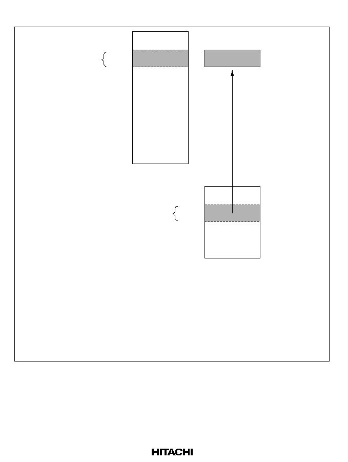
414
Example of Emulation of Real-Time Flash-Memory Update
H'007F
H'0080
H'00FF
H'0100
H'0000
H'7FFF
H'FB80
H'FC80
H'FCFF
H'FF7F
Small-block
area (SB1)
Flash memory
address space
Overlapped
RAM
Overlapped RAM
On-chip
RAM area
Procedure
1. Overlap part of RAM (H'FC80 to H'FCFF) onto the area requiring real-time update (SB1).
(Set WSCR bits 7 and 6 to 01.)
2. Perform real-time updates in the overlapping RAM.
3. After finalization of the update data, clear the RAM overlap (by clearing the RAMS and
RAM0 bits).
4. Read the data written in RAM addresses H'FC80 to H'FCFF out externally, then program
the flash memory area, using this data as part of the program data.
Figure 19.12 Example of RAM Overlap

415
Notes on Use of RAM Emulation Function
∑
Notes on Applying, Releasing, and Shutting Off the Programming Voltage (V
PP
)
Care is necessary to avoid errors in programming and erasing when applying, releasing, and
shutting off V
PP
, just as in the on-board programming modes. In particular, even if the
emulation function is being used, make sure that the watchdog timer is set when the P or E bit
of the flash memory control register (FLMCR) has been set, to prevent errors in programming
and erasing due to program runaway while V
PP
is applied.
For details see section 19.7, Flash Memory Programming and Erasing Precautions (5).

416
19.6
Flash Memory Writer Mode (H8/3334YF)
19.6.1
Writer Mode Setting
The on-chip flash memory of the H8/3334YF can be programmed and erased not only in the on-
board programming modes but also in writer mode, using a general-purpose PROM programmer.
19.6.2
Socket Adapter and Memory Map
Programs can be written and verified by attaching a socket adapter for the relevant package to the
PROM programmer. Table 19.12 gives ordering information for the socket adapter. Figure 19.13
shows a memory map in writer mode. Figure 19.14 shows the socket adapter pin interconnections.
Table 19.12
Socket Adapter
Microcontroller
Package
Socket Adapter
HD64F3334YF16
80-pin QFP
HS3334ESHF1H
HD64F3334YTF16
80-pin TQFP
HS3334ESNF1H
HD64F3334YCP16
84-pin PLCC
HS3334ESCF1H
H8/3334YF
H'0000
H'7FFF
H'0000
H'7FFF
On-chip ROM area
MCU mode
Writer mode
1 output
H'1FFFF
Figure 19.13 Memory Map in Writer Mode
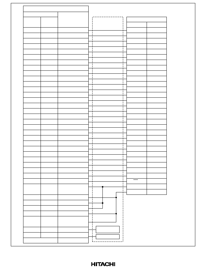
417
H8/3334YF
Pin Name
FP-80A
TFP-80C
CP-84
18
17
27
28
29
79
80
81
82
83
84
1
3
78
77
76
75
74
73
72
71
69
68
67
66
65
63
62
61
31, 32, 36,
37, 25
15, 16, 30, 40
42
19, 60
51
2, 4, 23, 24,
41, 64, 70
12
13, 14
7
6
15
16
17
65
66
67
68
69
70
71
72
64
63
62
61
60
59
58
57
55
54
53
52
51
50
49
48
19, 20,
24, 25, 13
4, 5, 18, 28
29
8, 47
38
12, 56,
73
1
2, 3
1
26
2
3
31
13
14
15
17
18
19
20
21
12
11
10
9
8
7
6
5
27
24
23
25
4
28
29
22
32
16
HN28F101 (32 Pins)
Pin No.
Pin Name
V
PP
FA
9
FA
16
FA
15
WE
FO
0
FO
1
FO
2
FO
3
FO
4
FO
5
FO
6
FO
7
FA
0
FA
1
FA
2
FA
3
FA
4
FA
5
FA
6
FA
7
FA
8
OE
FA
10
FA
11
FA
12
FA
13
FA
14
CE
V
CC
V
SS
Socket Adapter
Pin No.
STBY
/FV
PP
NMI
P9
5
P9
4
P9
3
P3
0
P3
1
P3
2
P3
3
P3
4
P3
5
P3
6
P3
7
P1
0
P1
1
P1
2
P1
3
P1
4
P1
5
P1
6
P1
7
P2
0
P2
1
P2
2
P2
3
P2
4
P2
5
P2
6
P2
7
P9
1
, P9
0
, P6
3
,
P6
4
, P9
7
MD
1
, MD
0
, P9
2,
P6
7
AV
CC
V
CC
AV
SS
V
SS
RES
XTAL, EXTAL
NC (OPEN)
Power-on
reset circuit
Oscillator circuit
Legend:
V
PP
:
FO
7
to FO
0
:
FA
16
to FA
0
:
OE
:
CE
:
WE
:
Programming power supply
Data input/output
Address input
Output enable
Chip enable
Write enable
Other pins
Figure 19.14 Wiring of Socket Adapter

418
19.6.3
Operation in Writer Mode
The program/erase/verify specifications in writer mode are the same as for the standard
HN28F101 flash memory. However, since the H8/3334YF does not support product name
recognition mode, the programmer cannot be automatically set with the device name. Table 19.13
indicates how to select the various operating modes.
Table 19.13
Operating Mode Selection in Writer Mode
Pins
Mode
FV
PP
V
CC
CE
OE
WE
D
7
to D
0
A
16
to A
0
Read
Read
V
CC
V
CC
L
L
H
Data output
Address input
Output
disable
V
CC
V
CC
L
H
H
High impedance
Standby
V
CC
V
CC
H
X
X
High impedance
Command
Read
V
PP
V
CC
L
L
H
Data output
write
Output
disable
V
PP
V
CC
L
H
H
High impedance
Standby
V
PP
V
CC
H
X
X
High impedance
Write
V
PP
V
CC
L
H
L
Data input
Note: Be sure to set the FV
PP
pin to V
CC
in these states. If it is set to 0 V, hardware standby mode
will be entered, even when in writer mode, resulting in incorrect operation.
Legend:
L:
Low level
H:
High level
V
PP
:
V
PP
level
V
CC
:
V
CC
level
X:
Don't care

419
Table 19.14
Writer Mode Commands
1st Cycle
2nd Cycle
Command
Cycles
Mode
Address
Data
Mode
Address
Data
Memory read
1
Write
X
H'00
Read
RA
Dout
Erase setup/erase
2
Write
X
H'20
Write
X
H'20
Erase-verify
2
Write
EA
H'A0
Read
X
EVD
Auto-erase setup/
auto-erase
2
Write
X
H'30
Write
X
H'30
Program setup/
program
2
Write
X
H'40
Write
PA
PD
Program-verify
2
Write
X
H'C0
Read
X
PVD
Reset
2
Write
X
H'FF
Write
X
H'FF
PA:
Program address
EA:
Erase-verify address
RA:
Read address
PD:
Program data
PVD:
Program-verify output data
EVD:
Erase-verify output data

420
High-Speed, High-Reliability Programming: Unused areas of the H8/3334YF flash memory
contain H'FF data (initial value). The H8/3334YF flash memory uses a high-speed, high-reliability
programming procedure. This procedure provides enhanced programming speed without
subjecting the device to voltage stress and without sacrificing the reliability of programmed data.
Figure 19.15 shows the basic high-speed, high-reliability programming flowchart. Tables 19.15
and 19.16 list the electrical characteristics during programming.
Start
Set V
PP
= 12.0 V
±
0.6 V
Address = 0
n = 0
Program command
Program setup command
n + 1
n
Wait (25
µ
s)
Program-verify command
Wait (6
µ
s)
Address + 1
address
Verification?
Last address?
Set V
PP
= V
CC
End
Fail
n = 20?
No go
No
Yes
Go
Yes
No
Figure 19.15 High-Speed, High-Reliability Programming

421
High-Speed, High-Reliability Erasing: The H8/3334YF flash memory uses a high-speed, high-
reliability erasing procedure. This procedure provides enhanced erasing speed without subjecting
the device to voltage stress and without sacrificing data reliability . Figure 19.16 shows the basic
high-speed, high-reliability erasing flowchart. Tables 19.15 and 19.16 list the electrical
characteristics during erasing.
Start
Program all bits to 0
*
Address = 0
n = 0
Wait (10 ms)
Erase setup/erase command
n + 1
n
Erase-verify command
Wait (6
µ
s)
Address + 1
address
Verification?
Last address?
End
Fail
n = 3000?
No go
No
Yes
Go
Yes
No
Follow the high-speed, high-reliability programming flowchart in programming all bits. If some bits
are already programmed to 0, program only the bits that have not yet been programmed.
Note:
*
Figure 19.16 High-Speed, High-Reliability Erasing

422
Table 19.15
DC Characteristics in Writer Mode
(Conditions: V
CC
= 5.0 V ±10%, V
PP
= 12.0 V ±0.6 V, V
SS
= 0 V, T
a
= 25∞C ±5∞C)
Item
Symbol
Min
Typ
Max
Unit
Test Conditions
Input high
voltage
FO
7
to FO
0
,
FA
16
to FA
0
,
OE
,
CE
,
WE
V
IH
2.2
--
V
CC
+ 0.3
V
Input low
voltage
FO
7
to FO
0
,
FA
16
to FA
0
,
OE
,
CE
,
WE
V
IL
≠0.3
--
0.8
V
Output high
voltage
FO
7
to FO
0
V
OH
2.4
--
--
V
I
OH
= ≠200 µA
Output low
voltage
FO
7
to FO
0
V
OL
--
--
0.45
V
I
OL
= 1.6 mA
Input leakage
current
FO
7
to FO
0
,
FA
16
to FA
0
,
OE
,
CE
,
WE
| I
LI
|
--
--
2
µA
Vin = 0 to V
CC
V
CC
current
Read
I
CC
--
40
80
mA
Program
I
CC
--
40
80
mA
Erase
I
CC
--
40
80
mA
FV
PP
current
Read
I
PP
--
--
10
µA
V
PP
= 5.0 V
--
10
20
mA
V
PP
= 12.6 V
Program
I
PP
--
20
40
mA
V
PP
= 12.6 V
Erase
I
PP
--
20
40
mA
V
PP
= 12.6 V

423
Table 19.16
AC Characteristics in Writer Mode
(Conditions: V
CC
= 5.0 V ±10%, V
PP
= 12.0 V ±0.6 V, V
SS
= 0 V, T
a
= 25∞C ±5∞C)
Item
Symbol
Min
Typ
Max
Unit
Test Conditions
Command write cycle
t
CWC
120
--
--
ns
Figure 19.17
Address setup time
t
AS
0
--
--
ns
Figure 19.18
*
Address hold time
t
AH
60
--
--
ns
Figure 19.19
Data setup time
t
DS
50
--
--
ns
Data hold time
t
DH
10
--
--
ns
CE
setup time
t
CES
0
--
--
ns
CE
hold time
t
CEH
0
--
--
ns
V
PP
setup time
t
VPS
100
--
--
ns
V
PP
hold time
t
VPH
100
--
--
ns
WE
programming pulse width
t
WEP
70
--
--
ns
WE
programming pulse high time
t
WEH
40
--
--
ns
OE
setup time before command write
t
OEWS
0
--
--
ns
OE
setup time before verify
t
OERS
6
--
--
µs
Verify access time
t
VA
--
--
500
ns
OE
setup time before status polling
t
OEPS
120
--
--
ns
Status polling access time
t
SPA
--
--
120
ns
Program wait time
t
PPW
25
--
--
ns
Erase wait time
t
ET
9
--
11
ms
Output disable time
t
DF
0
--
40
ns
Total auto-erase time
t
AET
0.5
--
30
s
Note:
CE
,
OE
, and
WE
should be high during transitions of V
PP
from 5 V to 12 V and from 12 V to
5 V.
*
Input pulse level: 0.45 V to 2.4 V
Input rise time and fall time
10 ns
Timing reference levels: 0.8 V and 2.0 V for input; 0.8 V and 2.0 V for output

424
Auto-erase setup
Auto-erase and status polling
Address
Command
input
Status polling
Command
input
Command
input
Command
input
5.0 V
12 V
5.0 V
V
CC
V
PP
CE
OE
WE
I/O7
I/O0 to I/O6
t
VPS
t
VPH
t
CEH
t
CES
t
CES
t
OEWS
t
WEP
t
CEH
t
CES
t
CWC
t
WEP
t
OEPS
t
AET
t
WEH
t
DS
t
DH
t
DS
t
DH
t
SPA
t
DF
Figure 19.17 Auto-Erase Timing
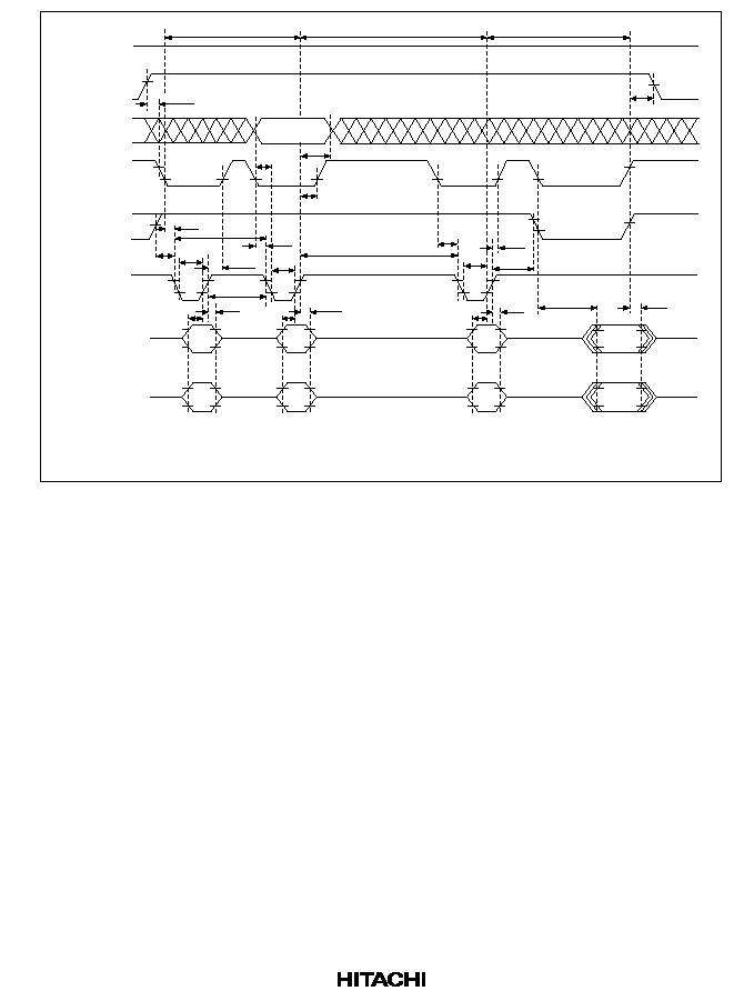
425
t
VPH
t
VPS
t
CEH
t
CES
t
OEWS
t
WEP
t
CEH
t
CES
t
CWC
t
WEP
t
DS
t
DH
t
DS
t
DH
t
AS
t
AH
t
PPW
t
CES
t
WEH
t
CEH
t
WEP
t
OERS
t
DH
t
DS
t
VA
t
DF
Command
input
Command
input
Data
input
Command
input
Command
input
Valid data
output
Data
input
Program setup
Program
Program-verify
Valid address
Address
5.0 V
12 V
5.0 V
V
CC
V
PP
CE
OE
WE
I/O7
I/O0 to I/O6
Note: Program-verify data output values may be intermediate between 1 and 0 before programming has
been completed.
Valid data
output
Figure 19.18 High-Speed, High-Reliability Programming Timing
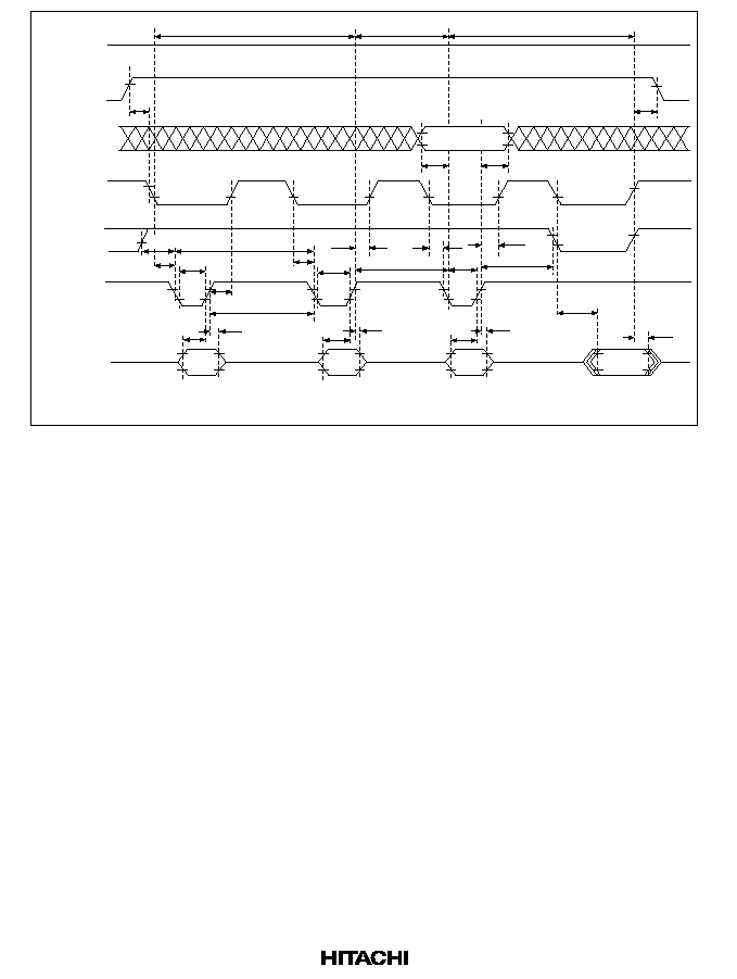
426
Address
5.0 V
12 V
5.0 V
V
CC
V
PP
CE
OE
WE
I/O0 to I/O7
Erase setup
Erase
Erase-verify
Valid address
Command
input
Command
input
Command
input
Valid data
output
t
VPS
t
VPH
t
AS
t
AH
t
OEWS
t
CWC
t
CES
t
WEP
t
CEH
t
DH
t
DS
t
WEH
t
DS
t
DH
t
DS
t
DH
t
VA
t
DF
t
CES
t
WEP
t
CEH
t
CES
t
ET
t
WEP
t
CEH
t
OERS
Note: Erase-verify data output values may be intermediate between 1 and 0 before erasing has been completed.
Figure 19.19 Erase Timing
19.7
Flash Memory Programming and Erasing Precautions
Read these precautions before using writer mode, on-board programming mode, or flash memory
emulation by RAM.
(1) Program with the specified voltages and timing.
The rated programming voltage (V
PP
) of the flash memory is 12.0 V.
If the PROM programmer is set to Hitachi HN28F101 specifications, V
PP
will be 12.0 V. Applying
voltages in excess of the rating can permanently damage the device. Take particular care to ensure
that the PROM programmer peak overshoot does not exceed the rated limit of 13 V.
(2) Before programming, check that the chip is correctly mounted in the PROM
programmer. Overcurrent damage to the device can result if the index marks on the PROM
programmer socket, socket adapter, and chip are not correctly aligned.
(3) Don't touch the socket adapter or chip while programming. Touching either of these can
cause contact faults and write errors.

427
(4) Set H'FF as the PROM programmer buffer data for addresses H'8000 to H'1FFFF. The
H8/3334YF PROM size is 32 kbytes. Addresses H'8000 to H'1FFFF always read H'FF, so if H'FF
is not specified as programmer data, a verify error will occur.
(5) Notes on applying, releasing, and shutting
*1
off the programming voltage (V
PP
)
∑
Apply the programming voltage (V
PP
) after the rise of V
CC
, and release V
PP
before shutting off
V
CC
.
To prevent unintended programming or erasing of flash memory, in these power-on and
power-off timings, the application, release, and shutting-off of V
PP
must take place when the
microcontroller is in a stable operating condition as defined below.
Stable operating condition
The V
CC
voltage must be stabilized within the rated voltage range (V
CC
= 2.7 V to 5.5 V)
*2
If V
PP
is applied, released, or shut off while the microcontroller's V
CC
voltage is not within
the rated voltage range (V
CC
= 2.7 to 5.5 V)
*2
, since microcontroller operation is unstable,
the flash memory may be programmed or erased by mistake. This can occur even if V
CC
=
0 V. To prevent changes in the V
CC
power supply when V
PP
is applied, be sure that the
power supply is adequately decoupled by inserting bypass capacitors.
Clock oscillation must be stabilized (the oscillation settling time must have elapsed), and
oscillation must not be stopped
When turning on V
CC
power, hold the
RES pin low during the oscillation settling time
(t
OSC1
= 20 ms), and do not apply V
PP
until after this time.
The microcontroller must be in the reset state, or in a state in which a reset has ended
normally (reset has been released) and flash memory is not being accessed
Apply or release V
PP
either in the reset state, or when the CPU is not accessing flash
memory (when a program in on-chip RAM or external memory is executing). Flash
memory cannot be read normally at the instant when V
PP
is applied or released. Do not read
flash memory while V
PP
is being applied or released.
For a reset during operation, apply or release V
PP
only after the
RES pin has been held low
for at least ten system clock cycles (10¯).
The P and E bits must be cleared in the flash memory control register (FLMCR)
When applying or releasing V
PP
, make sure that the P or E bit is not set by mistake.

428
No program runaway
When V
PP
is applied, program execution must be supervised, e.g. by the watchdog timer.
These power-on and power-off timing requirements should also be satisfied in the event of
a power failure and in recovery from a power failure. If these requirements are not
satisfied, overprogramming or overerasing may occur due to program runaway etc., which
could cause memory cells to malfunction.
∑
The V
PP
flag is set and cleared by a threshold decision on the voltage applied to the FV
PP
pin.
The threshold level is between approximately V
CC
+ 2 V to 11.4 V.
When this flag is set, it becomes possible to write to the flash memory control register
(FLMCR) and the erase block registers (EBR1 and EBR2), even though the V
PP
voltage may
not yet have reached the programming voltage range of 12.0 ± 0.6 V.
Do not actually program or erase the flash memory until V
PP
has reached the programming
voltage range.
The programming voltage range for programming and erasing flash memory is 12.0 ± 0.6 V
(11.4 V to 12.6 V). Programming and erasing cannot be performed correctly outside this range.
When not programming or erasing the flash memory, ensure that the V
PP
voltage does not
exceed the V
CC
voltage. This will prevent unintended programming and erasing.
∑
In this chip, the same pin is used for
STBY
and FV
PP
. When this pin is driven low, a transition
is made to hardware standby mode. This happens not only in the normal operating modes
(modes 1, 2, and 3), but also when programming the flash memory with a PROM programmer.
When programming with a PROM programmer, therefore, use a programmer which sets this
pin to the V
CC
level when not programming (FV
PP
= 12 V).
Notes: *1 In this section, the application, release, and shutting-off of V
PP
are defined as follows.
Application:
A rise in voltage from V
CC
to 12 V ± 0.6 V.
Release:
A drop in voltage from 12 V ± 0.6 V to V
CC
.
Shut-off:
No applied voltage (floating).
*2 In the LH version, V
CC
= 3.0 V to 5.5 V.
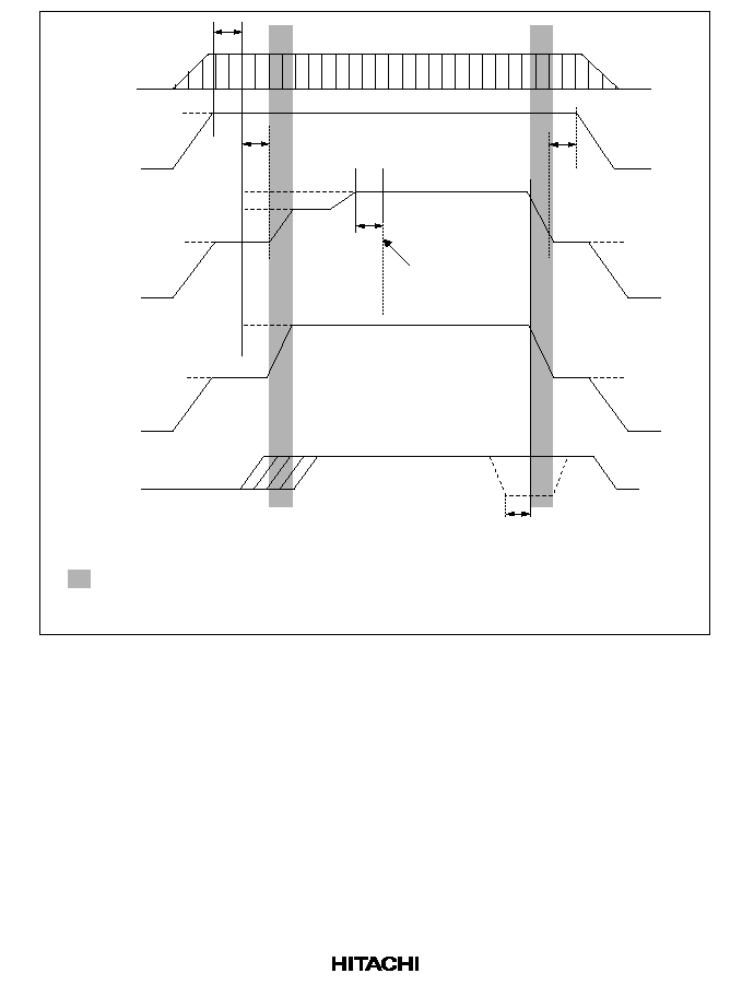
429
t
OSC1
2.7 to 5.5 V
*
12
±
0.6 V
V
CC
+ 2 V to 11.4 V
V
CC
V
12
±
0.6 V
V
CC
V
0
µ
s min
0
µ
s min
0
µ
s min
0 to V
CC
V
0 to V
CC
V
Min 10¯
(when
RES
is low)
¯
V
CC
V
PP
V
PP
RES
Boot mode
User program
mode
Timing at which boot
program branches
to RAM area
Periods during which the V
PP
flag is being set or
cleared and flash memory must not be accessed
Note:
*
In the LH version, V
CC
= 3.0 V to 5.5 V.
Figure 19.20 V
PP
Power-On and Power-Off Timing
(6) Do not apply 12 V to the FV
PP
pin during normal operation.
To prevent accidental programming or erasing due to microcontroller program runaway etc., apply
12 V to the V
PP
pin only when the flash memory is programmed or erased, or when flash memory
is emulated by RAM. Overprogramming or overerasing due to program runaway can cause
memory cells to malfunction. Avoid system configurations in which 12 V is always applied to the
FV
PP
pin.
While 12 V is applied, the watchdog timer should be running and enabled to halt runaway
program execution, so that program runaway will not lead to overprogramming or overerasing.

430
(7) Design a current margin into the programming voltage (V
PP
) power supply. Ensure that
V
PP
will not depart from 12.0 ±0.6 V (11.4 V to 12.6 V) during programming or erasing.
Programming and erasing may become impossible outside this range.
(8) Ensure that peak overshoot does not exceed the rated value at the FV
PP
and MD
1
pins.
Connect decoupling capacitors as close to the FV
PP
and MD
1
pins as possible.
Also connect decoupling capacitors to the MD
1
pin in the same way when boot mode is uesd.
0.01
µ
F
1.0
µ
F
12 V
FV
PP
H8/3334YF
Figure 19.21 V
PP
Power Supply Circuit Design (Example)
(9) Use the recommended algorithms for programming and erasing flash memory. These
algorithms are designed to program and erase without subjecting the device to voltage stress and
without sacrificing the reliability of programmed data.
Before setting the program (P) or erase (E) bit in the flash memory control register (FLMCR), set
the watchdog timer to ensure that the P or E bit does not remain set for more than the specified
time.
(10) For details on interrupt handling while flash memory is being programmed or erased,
see the notes on NMI interrupt handling in section 19.4.9, Interrupt Handling during Flash
Memory Programming and Erasing.

431
(11) Cautions on Accessing Flash Memory Control Registers
1. Flash memory control register access state in each operating mode
The H8/3334YF has flash memory control registers located at addresses H'FF80 (FLMCR),
H'FF82 (EBR1), and H'FF83 (EBR2). These registers can only be accessed when 12 V is
applied to the flash memory program power supply pin, FV
PP
.
Table 19.17 shows the area accessed for the above addresses in each mode, when 12 V is and
is not applied to FV
PP
.
Table 19.17
Area Accessed in Each Mode with 12V Applied and Not Applied to FV
PP
Mode 1
Mode 2
Mode 3
12 V applied to FV
PP
register
Reserved area
(always H'FF)
Flash memory control
register (initial value H'80)
Flash memory control
(initial value H'80)
12 V not applied to
FV
PP
External address
space
External address space
Reserved area (always
H'FF)
2. When a flash memory control register is accessed in mode 2 (expanded mode with on-chip
ROM enabled)
When a flash memory control register is accessed in mode 2, it can be read or written to if
12 V is being applied to FV
PP
, but if not, external address space will be accessed. It is therefore
essential to confirm that 12 V is being applied to the FV
PP
pin before accessing these registers.
3. To check for 12 V application/non-application in mode 3 (single-chip mode)
When address H'FF80 is accessed in mode 3, if 12 V is being applied to FV
PP
, FLMCR is
read/written to, and its initial value after reset is H'80. When 12 V is not being applied to FV
PP
,
FLMCR is a reserved area that cannot be modified and always reads H'FF. Since bit 7
(corresponding to the V
PP
bit) is set to 1 at this time regardless of whether 12 V is applied to
FV
PP
, application or release of 12 V to FV
PP
cannot be determined simply from the 0 or 1 status
of this bit. A byte data comparison is necessary to check whether 12 V is being applied. The
relevant coding is shown below.
.
.
.
LABEL1: MOV.B @H'FF80, R1L
CMP.B #H'FF, R1L
BEQ LABEL1
.
.
.
Sample program for detection of 12 V application to FV
PP
(mode 3)

432
Table 19.18
DC Characteristics of Flash Memory
Conditions: V
CC
= 2.7 V to 5.5 V
*2
, AV
CC
= 2.7 V to 5.5 V
*2
,V
SS
= AV
SS
= 0 V,
V
PP
= 12.0 ± 0.6 V, T
a
= ≠20∞C to +75∞C (regular specifications), T
a
= ≠40∞C to
+85∞C (wide-range specifications)
Item
Symbol
Min
Typ
Max
Unit
Test Conditions
High-voltage (12 V)
threshold level
*
1
FV
PP
, MD
1
V
H
V
CC
+ 2
--
11.4
V
FV
PP
current
During read
I
PP
--
--
10
µA
V
PP
= 2.7 to 5.5 V
--
10
20
mA
V
PP
= 12.6 V
During
programming
--
20
40
mA
During erasure
--
20
40
mA
Notes:
*
1 The listed voltages indicate the threshold level at which high-voltage application is
recognized. In boot mode and while flash memory is being programmed or erased, the
applied voltage should be 12.0 V ± 0.6 V.
*
2 In the LH version, V
CC
= 3.0 V to 5.5 V, AV
CC
= 3.0 V to 5.5 V
Table 19.19
AC Characteristics of Flash Memory
Conditions: V
CC
= 2.7 V to 5.5 V
*5
, AV
CC
= 2.7 V to 5.5 V
*5
, V
SS
= AV
SS
= 0 V,
V
PP
= 12.0 ± 0.6 V, T
a
= ≠20∞C to +75∞C (regular specifications), T
a
= ≠40∞C to
+85∞C (wide-range specifications)
Item
Symbol
Min
Typ
Max
Unit
Test Conditions
Programming time
*
1,
*
2
t
P
--
50
1000
µs
Erase time
*
1,
*
3
t
E
--
1
30
s
Number of writing/erasing count
N
WEC
--
--
100
Times
Verify setup time 1
*
1
t
VS1
4
--
--
µs
Verify setup time 2
*
1
t
VS2
2
--
--
µs
Flash memory read setup time
*
4
t
FRS
50
--
--
µs
V
CC
4.5 V
100
--
--
V
CC
< 4.5 V
Notes:
*
1 Set the times following the programming/erasing algorithm shown in section 19.
*
2 The programming time is the time during which a byte is programmed or the P bit in the
flash memory control register (FLMCR) is set. It does not include the program-verify
time.
*
3 The erase time is the time during which all 32-kbyte blocks are erased or the E bit in the
flash memory control register (FLMCR) is set. It does not include the prewrite time
before erasure or erase-verify time.
*
4 After power-on when using an external clock source, after return from standby mode, or
after switching the programming voltage (V
PP
) from 12 V to V
CC
, make sure that this read
setup time has elapsed before reading flash memory.
When V
PP
is released, the flash memory read setup time is defined as the period from
when the FV
PP
pin has reached V
CC
+ 2 V until flash memory can be read.
*
5 In the LH version, V
CC
= 3.0 V to 5.5 V, AV
CC
= 3.0 V to 5.5 V.

433
Section 20 ROM
(60-kbyte Dual-Power-Supply Flash Memory Version)
20.1
Flash Memory Overview
20.1.1
Flash Memory Operating Principle
Table 20.1 illustrates the principle of operation of the H8/3337YF's on-chip flash memory.
Like EPROM, flash memory is programmed by applying a high gate-to-drain voltage that draws
hot electrons generated in the vicinity of the drain into a floating gate. The threshold voltage of a
programmed memory cell is therefore higher than that of an erased cell. Cells are erased by
grounding the gate and applying a high voltage to the source, causing the electrons stored in the
floating gate to tunnel out. After erasure, the threshold voltage drops. A memory cell is read like
an EPROM cell, by driving the gate to the high level and detecting the drain current, which
depends on the threshold voltage. Erasing must be done carefully, because if a memory cell is
overerased, its threshold voltage may become negative, causing the cell to operate incorrectly.
Section 20.4.6 shows an optimal erase control flowchart and sample program.
Table 20.1
Principle of Memory Cell Operation
Program
Erase
Read
Memory
cell
Vd
Vg = V
PP
Open
Vs = V
PP
Vd
Vg
Memory
array
Vd
0 V
V
PP
0 V
0 V
Open
Open
0 V
V
PP
0 V
Vd
0 V
V
CC
0 V
0 V

434
20.1.2
Mode Programming and Flash Memory Address Space
As its on-chip ROM, the H8/3337YF has 60 kbytes of flash memory. The flash memory is
connected to the CPU by a 16-bit data bus. The CPU accesses both byte data and word data in two
states.
The H8/3337YF's flash memory is assigned to addresses H'0000 to H'EF7F in mode2, and
addresses H'0000 to H'F77F in mode3. The mode pins enable either on-chip flash memory or
external memory to be selected for this area. Table 20.2 summarizes the mode pin settings and
usage of the memory area.
Table 20.2
Mode Pin Settings and Flash Memory Area
Mode Pin Setting
Mode
MD
1
MD
0
Memory Area Usage
Mode 0
0
0
Illegal setting
Mode 1
0
1
External memory area
Mode 2
1
0
On-chip flash memory area (H'0000 to H'EF7F)
Mode 3
1
1
On-chip flash memory area (H'0000 to H'F77F)
20.1.3
Features
Features of the flash memory are listed below.
∑
Five flash memory operating modes
The flash memory has five operating modes: program mode, program-verify mode, erase
mode, erase-verify mode, and prewrite-verify mode.
∑
Block erase designation
Blocks to be erased in the flash memory address space can be selected by bit settings. The
address space includes a large-block area (eight blocks with sizes from 2 kbytes to 12 kbytes)
and a small-block area (eight blocks with sizes from 128 bytes to 1 kbyte).
∑
Program and erase time
Programming one byte of flash memory typically takes 50 µs, while erasing typically takes 1 s.
∑
Erase-program cycles
Flash memory contents can be erased and reprogrammed up to 100 times.
∑
On-board programming modes
These modes can be used to program, erase, and verify flash memory contents. There are two
modes: boot mode and user programming mode.
435
∑
Automatic bit-rate alignment
In boot-mode data transfer, the H8/3337YF aligns its bit rate automatically to the host bit rate
(maximum 9600 bps).
∑
Flash memory emulation by RAM
Part of the RAM area can be overlapped onto flash memory, to emulate flash memory updates
in real time.
∑
Writer mode
As an alternative to on-board programming, the flash memory can be programmed and erased
in writer mode, using a general-purpose PROM programmer. Program, erase, verify, and other
specifications are the same as for HN28F101 standard flash memory.
20.1.4
Block Diagram
Figure 20.1 shows a block diagram of the flash memory.
FLMCR
EBR1
EBR2
H'0000
H'0002
H'0004
H'F77C
H'F77E
H'0001
H'0003
H'0005
H'F77D
H'F77F
MD
1
MD
0
Internal data bus (upper)
Internal data bus (lower)
Bus interface and control section
Operating
mode
On-chip flash memory
(60 kbytes)
Upper byte
(even address)
Lower byte
(odd address)
Legend:
FLMCR:
EBR1:
EBR2:
Flash memory control register
Erase block register 1
Erase block register 2
8
8
Figure 20.1 Flash Memory Block Diagram

436
20.1.5
Input/Output Pins
Flash memory is controlled by the pins listed in table 20.3.
Table 20.3
Flash Memory Pins
Pin Name
Abbreviation
Input/Output
Function
Programming power
FV
PP
Power supply
Apply 12.0 V
Mode 1
MD
1
Input
H8/3337YF operating mode setting
Mode 0
MD
0
Input
H8/3337YF operating mode setting
Transmit data
TxD
1
Output
SCI1 transmit data output
Receive data
RxD
1
Input
SCI1 receive data input
The transmit data and receive data pins are used in boot mode.
20.1.6
Register Configuration
The flash memory is controlled by the registers listed in table 20.4.
Table 20.4
Flash Memory Registers
Name
Abbreviation
R/W
Initial Value
Address
Flash memory control register
FLMCR
R/W
*
2
H'00
*
2
H'FF80
Erase block register 1
EBR1
R/W
*
2
H'00
*
2
H'FF82
Erase block register 2
EBR2
R/W
*
2
H'00
*
2
H'FF83
Wait-state control register
*
1
WSCR
R/W
H'08
H'FFC2
Notes:
*
1 The wait-state control register controls the insertion of wait states by the wait-state
controller, frequency division of clock signals for the on-chip supporting modules by the
clock pulse generator, and emulation of flash-memory updates by RAM in on-board
programming mode.
*
2 In modes 2 and 3 (on-chip flash memory enabled), the initial value is H'00 for FLMCR,
EBR1 and EBR2. In mode 1 (on-chip flash memory disabled), these registers cannot be
modified and always read H'FF.
Registers FLMCR, EBR1, and EBR2 are only valid when writing to or erasing flash memory, and
can only be accessed while 12 V is being applied to the FV
PP
pin. When 12 V is not applied to the
FV
PP
pin, in mode 2 addresses H'FF80 to H'FF83 are external address space, and in mode 3 these
addresses cannot be modified and always read H'FF.
437
20.2
Flash Memory Register Descriptions
20.2.1
Flash Memory Control Register (FLMCR)
FLMCR is an 8-bit register that controls the flash memory operating modes. Transitions to
program mode, erase mode, program-verify mode, and erase-verify mode are made by setting bits
in this register. FLMCR is initialized to H'00 by a reset, in the standby modes, and when 12 V is
not applied to FV
PP
. When 12 V is applied to the FV
PP
pin, a reset or entry to a standby mode
initializes FLMCR to H'80.
Bit
7
6
5
4
3
2
1
0
V
PP
--
--
--
EV
PV
E
P
Initial value
0
0
0
0
0
0
0
0
Read/Write
R
--
--
--
R/W
*
R/W
*
R/W
*
R/W
*
Note:
*
The initial value is H'00 in modes 2 and 3 (on-chip flash memory enabled). In mode 1 (on-
chip flash memory disabled), this register cannot be modified and always reads H'FF. For
information on accessing this register, refer to in section 20.7, Flash Memory Programming
and Erasing Precautions (11).
Bit 7--Programming Power (V
PP
): This status flag indicates that 12 V is applied to the FV
PP
pin.
Refer to section 20.7, Flash Memory Programming and Erasing Precautions (5), for details on use.
Bit 7: V
PP
Description
0
Cleared when 12 V is not applied to FV
PP
(Initial value)
1
Set when 12 V is applied to FV
PP
Bits 6 to 4--Reserved: These bits cannot be modified, and are always read as 0.
Bit 3--Erase-Verify Mode (EV):
*1
Selects transition to or exit from erase-verify mode.
Bit 3: EV
Description
0
Exit from erase-verify mode
(Initial value)
1
Transition to erase-verify mode
Bit 2--Program-Verify Mode (PV):
*1
Selects transition to or exit from program-verify mode.
Bit 2: PV
Description
0
Exit from program-verify mode
(Initial value)
1
Transition to program-verify mode

438
Bit 1--Erase Mode (E):
*1, *2
Selects transition to or exit from erase mode.
Bit 1: E
Description
0
Exit from erase mode
(Initial value)
1
Transition to erase mode
Bit 0--Program Mode (P):
*1, *2
Selects transition to or exit from program mode.
Bit 0: P
Description
0
Exit from program mode
(Initial value)
1
Transition to program mode
Notes: *1 Do not set two or more of these bits simultaneously. Do not release or shut off the V
CC
or V
PP
power supply when these bits are set.
*2 Set the P or E bit according to the instructions given in section 20.4, Programming and
Erasing Flash Memory.
Set the watchdog timer beforehand to make sure that these bits do not remain set for
longer than the specified times.
For notes on use, see section 20.7, Flash Memory Programming and Erasing
Precautions.
20.2.2
Erase Block Register 1 (EBR1)
EBR1 is an 8-bit register that designates large flash-memory blocks for programming and erasure.
EBR1 is initialized to H'00 by a reset, in the standby modes, and when 12 V is not applied to the
FV
PP
pin. When a bit in EBR1 is set to 1, the corresponding block is selected and can be
programmed and erased. Figure 20.2 and table 20.6 show details of a block map.
Bit
7
6
5
4
3
2
1
0
LB7
LB6
LB5
LB4
LB3
LB2
LB1
LB0
Initial value
*
1
0
0
0
0
0
0
0
0
Read/Write
R/W
*
1,
*
2
R/W
*
1
R/W
*
1
R/W
*
1
R/W
*
1
R/W
*
1
R/W
*
1
R/W
*
1
Notes:
*
1 The initial value is H'00 in modes 2 and 3 (on-chip ROM enabled). In mode 1 (on-chip
ROM disabled), this register cannot be modified and always reads H'FF.
*
2 This bit cannot be modified mode 2.
For information on accessing this register, refer to in section 20.7, Flash Memory
Programming and Erasing Precautions (11).

439
Bits 7 to 0--Large Block 7 to 0 (LB7 to LB0): These bits select large blocks (LB7 to LB0) to be
programmed and erased.
Bits 7 to 0:
LB7 to LB0
Description
0
Block (LB7 to LB0) is not selected
(Initial value)
1
Block (LB7 to LB0) is selected
20.2.3
Erase Block Register 2 (EBR2)
EBR2 is an 8-bit register that designates small flash-memory blocks for programming and erasure.
EBR2 is initialized to H'00 by a reset, in the standby modes, and when 12 V is not applied to the
FV
PP
pin. When a bit in EBR2 is set to 1, the corresponding block is selected and can be
programmed and erased. Figure 20.2 and table 20.6 show a block map.
Bit
7
6
5
4
3
2
1
0
SB7
SB6
SB5
SB4
SB3
SB2
SB1
SB0
Initial value
*
0
0
0
0
0
0
0
0
Read/Write
R/W
*
R/W
*
R/W
*
R/W
*
R/W
*
R/W
*
R/W
*
R/W
*
Note:
*
The initial value is H'00 in modes 2 and 3 (on-chip ROM enabled). In mode 1 (on-chip ROM
disabled), this register cannot be modified and always reads H'FF.
For information on accessing this register, refer to in section 20.7, Flash Memory
Programming and Erasing Precautions (11).
Bits 7 to 0--Small Block 7 to 0 (SB7 to SB0): These bits select small blocks (SB7 to SB0) to be
programmed and erased.
Bits 7 to 0:
SB7 to SB0
Description
0
Block (SB7 to SB0) is not selected
(Initial value)
1
Block (SB7 to SB0) is selected

440
20.2.4
Wait-State Control Register (WSCR)
WSCR is an 8-bit readable/writable register that enables flash-memory updates to be emulated in
RAM. It also controls frequency division of clock signals supplied to the on-chip supporting
modules and insertion of wait states by the wait-state controller.
WSCR is initialized to H'08 by a reset and in hardware standby mode. It is not initialized in
software standby mode.
Bit
7
6
5
4
3
2
1
0
RAMS
RAM0
CKDBL
--
WMS1
WMS0
WC1
WC0
Initial value
0
0
0
0
1
0
0
0
Read/Write
R/W
R/W
R/W
R/W
R/W
R/W
R/W
R/W
Bits 7 and 6--RAM Select and RAM0 (RAMS and RAM0): These bits are used to reassign an
area to RAM (see table 20.5). These bits are write-enabled and their initial value is 0. They are
initialized by a reset and in hardware standby mode. They are not initialized in software standby
mode.
If only one of bits 7 and 6 is set, part of the RAM area can be overlapped onto the small-block
flash memory area. In that case, access is to RAM, not flash memory, and all flash memory blocks
are write/erase-protected (emulation protect
*1
). In this state, the mode cannot be changed to
program or erase mode, even if the P bit or E bit in the flash memory control register (FLMCR) is
set (although verify mode can be selected). Therefore, clear both of bits 7 and 6 before
programming or erasing the flash memory area.
If both of bits 7 and 6 are set, part of the RAM area can be overlapped onto the small-block flash
memory area, but this overlapping begins only when an interrupt signal is input while 12 V is
being applied to the FV
PP
pin. Up until that point, flash memory is accessed. Use this setting for
interrupt handling while flash memory is being programmed or erased.
*2
Table 20.5
RAM Area Reassignment
*3
Bit 7: RAMS
Bit 6: RAM0
RAM Area
ROM Area
0
0
None
--
1
H'F880 to H'F8FF
H'0080 to H'00FF
1
0
H'F880 to H'F97F
H'0080 to H'017F
1
H'F800 to H'F87F
H'0000 to H'007F

441
Bit 5--Clock Double (CKDBL): Controls frequency division of clock signals supplied to the on-
chip supporting modules. For details, see section 6, Clock Pulse Generator.
Bit 4--Reserved: This bit is reserved, but it can be written and read. Its initial value is 0.
Bits 3 and 2--Wait Mode Select 1 and 0 (WMS1, WMS0)
Bits 1 and 0--Wait Count 1 and 0 (WC1, WC0)
These bits control insertion of wait states by the wait-state controller. For details, see section 5,
Wait-State Controller.
Notes: *1 For details on emulation protect, see section 20.4.8, Protect Modes.
*2 For details on interrupt handling during programming and erasing of flash memory, see
section 20.4.9, Interrupt Handling during Flash Memory Programming and Erasing.
*3 RAM area that overlaps flash memory.

442
H'0000
H'01FF
H'0200
H'03FF
H'0400
H'07FF
H'0800
H'0BFF
H'0C00
H'0FFF
H'0000
H'0FFF
H'1000
H'1FFF
H'2000
H'3FFF
H'4000
H'5FFF
H'6000
H'9FFF
H'A000
H'BFFF
H'C000
H'EF7F
H'EF80
H'7FFF
H'8000
H'F77F
Small block
area
(4 kbytes)
Large block
area
(58 kbytes)
SB7 to SB0
4 kbytes
LB0
4 kbytes
LB1
8 kbytes
LB7
2 kbytes
SB0 128 bytes
SB1 128 bytes
SB2 128 bytes
SB3 128 bytes
LB2
8 kbytes
LB3
8 kbytes
SB4
512 bytes
SB5
1 kbyte
SB6
1 kbyte
SB7
1 kbyte
LB4
8 kbytes
LB5
8 kbytes
LB6
12 kbytes
Figure 20.2 Erase Block Map

443
Table 20.6
Erase Blocks and Corresponding Bits
Register
Bit
Block
Address
Size
EBR1
0
LB0
H'1000 to H'1FFF
4 kbytes
1
LB1
H'2000 to H'3FFF
8 kbytes
2
LB2
H'4000 to H'5FFF
8 kbytes
3
LB3
H'6000 to H'7FFF
8 kbytes
4
LB4
H'8000 to H'9FFF
8 kbytes
5
LB5
H'A000 to H'BFFF
8 kbytes
6
LB6
H'C000 to H'EF7F
12 kbytes
7
LB7
H'EF80 to H'F77F
2 kbytes
EBR2
0
SB0
H'0000 to H'007F
128 bytes
1
SB1
H'0080 to H'00FF
128 bytes
2
SB2
H'0100 to H'017F
128 bytes
3
SB3
H'0180 to H'01FF
128 bytes
4
SB4
H'0200 to H'03FF
512 bytes
5
SB5
H'0400 to H'07FF
1 kbyte
6
SB6
H'0800 to H'0BFF
1 kbyte
7
SB7
H'0C00 to H'0FFF
1 kbyte
20.3
On-Board Programming Modes
When an on-board programming mode is selected, the on-chip flash memory can be programmed,
erased, and verified. There are two on-board programming modes: boot mode, and user
programming mode. These modes are selected by inputs at the mode pins (MD
1
and MD
0
) and
FV
PP
pin. Table 20.7 indicates how to select the on-board programming modes. For details on
applying voltage V
PP
, refer to section 20.7, Flash Memory Programming and Erasing Precautions
(5).

444
Table 20.7
On-Board Programming Mode Selection
Mode Selections
FV
PP
MD
1
MD
0
Notes
Boot mode
Mode 2
12 V
*
12 V
*
0
0: V
IL
Mode 3
12 V
*
1
1: V
IH
User programming
Mode 2
1
0
mode
Mode 3
1
1
Note:
*
For details on the timing of 12 V application, see notes 6 to 8 in the Notes on Use of Boot
Mode at the end of this section.
In boot mode, the mode control register (MDCR) can be used to monitor the mode (mode 2
or 3) in the same way as in normal mode.
Example: Set the mode pins for mode 2 boot mode (MD
1
= 12 V, MD
0
= 0 V).
If the mode select bits of MDCR are now read, they will indicate mode 2 (MDS1 = 1,
MDS0 = 0).
20.3.1
Boot Mode
To use boot mode, a user program for programming and erasing the flash memory must be
provided in advance on the host machine (which may be a personal computer). Serial
communication interface channel 1 is used in asynchronous mode. If the H8/3337YF is placed in
boot mode, after it comes out of reset, a built-in boot program is activated. This program starts by
measuring the low period of data transmitted from the host and setting the bit rate register (BRR)
accordingly. The H8/3337YF's built-in serial communication interface (SCI) can then be used to
download the user program from the host machine. The user program is stored in on-chip RAM.
After the program has been stored, execution branches to address H'F7E0 in the on-chip RAM,
and the program stored on RAM is executed to program and erase the flash memory. Figure 20.4
shows the boot-mode execution procedure.
HOST
Receive data to be programmed
Transmit verification data
H8/3337YF
RxD
1
TxD
1
SCI
Figure 20.3 Boot-Mode System Configuration

445
Boot-Mode Execution Procedure: Figure 20.4 shows the boot-mode execution procedure.
Start
Program H8/3337YF pins for boot mode,
and reset
Host transmits H'00 data continuously
at desired bit rate
H8/3337YF measures low period
of H'00 data transmitted from host
H8/3337YF computes bit rate and
sets bit rate register
After completing bit-rate alignment, H8/3337YF
sends one H'00 data byte to host to indicate
that alignment is completed
Host checks that this byte, indicating
completion of bit-rate alignment, is received
normally, then transmits one H'55 byte
After receiving H'55, H8/3337YF sends part of
the boot program to RAM
H8/3337YF transfers one user program
byte to RAM
*
2
H8/3337YF calculates number of bytes left
to be transferred (N = N ≠ 1)
All bytes transferred?
(N = 0?)
All data = H'FF?
*
4
Erase all flash
memory blocks
*
3,
*
4
After transferring the user program to RAM,
H8/3337YF transmits one H'AA data byte to host
No
Yes
Yes
No
1
2
3
4
5
6
7
9
H8/3337YF branches to the RAM boot
area (H'F800 to H'FF2F), then checks the
data in the user area of flash memory
H8/3337YF receives two bytes indicating byte
length (N) of program to be downloaded
to on-chip RAM
*
1
8
After checking that all data in flash memory is H'FF,
H8/3337YF transmits one H'AA data byte to host
H8/3337YF branches to H'F7E0 in RAM area and
executes user program downloaded into RAM
10
1. Program the H8/3337YF pins for boot mode, and start the
H8/3337YF from a reset.
2. Set the host's data format to 8 bits + 1 stop bit, select the
desired bit rate (2400, 4800, or 9600 bps), and transmit
H'00 data continuously.
3. The H8/3337YF repeatedly measures the low period of
the RxD1 pin and calculates the host's asynchronous-
communication bit rate.
4. When SCI bit-rate alignment is completed, the
H8/3337YF transmits one H'00 data byte to indicate
completion of alignment.
5. The host should receive the byte transmitted from the
H8/3337YF to indicate that bit-rate alignment is
completed, check that this byte is received normally, then
transmit one H'55 byte.
6. After receiving H'55, H8/3337YF sends part of the boot
program to H'F780 to H'F7DF and H'F800 to H'FF2F of
RAM.
7. After branching to the boot program area (H'F800 to
H'FF2F) in RAM, the H8/3337YF checks whether the
flash memory already contains any programmed data. If
so, all blocks are erased.
8. After the H8/3337YF transmits one H'AA data byte, the
host transmits the byte length of the user program to be
transferred to the H8/3337YF. The byte length must be
sent as two-byte data, upper byte first and lower byte
second. After that, the host proceeds to transmit the user
program. As verification, the H8/3337YF echoes each
byte of the received byte-length data and user program
back to the host.
9. The H8/3337YF stores the received user program in on-
chip RAM in a 1934-byte area from H'F7E0 to H'FF6D.
10. After transmitting one H'AA data byte, the H8/3337YF
branches to address H'F7E0 in on-chip RAM and
executes the user program stored in the area from
H'F7E0 to H'FF6D.
Notes:
*
1 The user can use 1934 bytes of RAM. The
number of bytes transferred must not exceed 1934
bytes. Be sure to transmit the byte length in two
bytes, upper byte first and lower byte second. For
example, if the byte length of the program to be
transferred is 256 bytes (H'0100), transmit H'01 as
the upper byte, followed by H'00 as the lower byte.
*
2 The part of the user program that controls the
flash memory should be coded according to the
flash memory write/erase algorithms given later.
*
3 If a memory cell malfunctions and cannot be
erased, the H8/3337YF transmits one H'FF byte to
report an erase error, halts erasing, and halts
further operations.
*
4 H'0000 to H'EF7F in mode2 and H'0000 to H'F77F
in mode 3.
Figure 20.4 Boot Mode Flowchart

446
Automatic Alignment of SCI Bit Rate
D0
D1
D2
D3
D4
D5
D6
D7
Start
bit
Stop
bit
This low period (9 bits) is measured (H'00 data)
High for at
least 1 bit
Figure 20.5 Measurement of Low Period in Data Transmitted from Host
When started in boot mode, the H8/3337YF measures the low period in asynchronous SCI data
transmitted from the host (figure 20.5). The data format is eight data bits, one stop bit, and no
parity bit. From the measured low period (9 bits), the H8/3337YF computes the host's bit rate.
After aligning its own bit rate, the H8/3337YF sends the host 1 byte of H'00 data to indicate that
bit-rate alignment is completed. The host should check that this alignment-completed indication is
received normally and send one byte of H'55 back to the H8/3337YF. If the alignment-completed
indication is not received normally, the H8/3337YF should be reset, then restarted in boot mode to
measure the low period again. There may be some alignment error between the host's and
H8/3337YF's bit rates, depending on the host's bit rate and the H8/3337YF's system clock
frequency. To have the SCI operate normally, set the host's bit rate to 2400, 4800, or 9600 bps
*1
.
Table 20.8 lists typical host bit rates and indicates the clock-frequency ranges over which the
H8/3337YF can align its bit rate automatically. Boot mode should be used within these frequency
ranges
*2
.
Table 20.8
System Clock Frequencies Permitting Automatic Bit-Rate Alignment by
H8/3337YF
Host Bit Rate
*
1
System Clock Frequencies Permitting Automatic Bit-Rate Alignment
by H8/3337YF
9600 bps
8 MHz to 16 MHz
4800 bps
4 MHz to 16 MHz
2400 bps
2 MHz to 16 MHz
Notes:
*
1 Use a host bit rate setting of 2400, 4800, or 9600 bps only. No other setting should be
used.
*
2 Although the H8/3337YF may also perform automatic bit-rate alignment with bit rate
and system clock combinations other than those shown in table 20.8, there will be a
slight difference between the bit rates of the host and the H8/3337YF, and subsequent
transfer will not be performed normally. Therefore, only a combination of bit rate and
system clock frequency within one of the ranges shown in table 20.8 can be used for
boot mode execution.

447
RAM Area Allocation in Boot Mode: In boot mode, the 96 bytes from H'F780 to H'F7DF and
the 18 bytes from H'FF6E to H'FF7F are reserved for use by the boot program, as shown in figure
20.6. The user program is transferred into the area from H'F7E0 to H'FF6D (1934 bytes). The boot
program area can be used after the transition to execution of the user program transferred into
RAM. If a stack area is needed, set it within the user program.
User program
transfer area
(1934 bytes)
Boot program
area
*
(18 bytes)
Boot program
area
*
(96 bytes)
H'F780
H'F7E0
H'FF6E
H'FF7F
Note:
*
This area cannot be used until the H8/3337YF starts to execute the user program
transferred to RAM (until it has branched to H'F7E0 in RAM). Note that even after the
branch to the user program, the boot program area (H'F780 to H'F7DF, H'FF6E to
H'FF7F) still contains the boot program.
Note also that 16 bytes (H'F780 to H'F78F) of this area cannot be used if an interrupt
handling routine is executed within the boot program. For details see section 20.4.9,
Interrupt Handling during Flash Memory Programming and Erasing.
Figure 20.6 RAM Areas in Boot Mode

448
Notes on Use of Boot Mode
1. When the H8/3337YF comes out of reset in boot mode, it measures the low period of the input
at the SCI's RxD
1
pin. The reset should end with RxD
1
high. After the reset ends, it takes about
100 states for the H8/3337YF to get ready to measure the low period of the RxD
1
input.
2. In boot mode, if any data has been programmed into the flash memory (if all data
*3
is not
H'FF), all flash memory blocks are erased. Boot mode is for use when user programming mode
is unavailable, e.g. the first time on-board programming is performed, or if the update program
activated in user programming mode is accidentally erased.
3. Interrupts cannot be used while the flash memory is being programmed or erased.
4. The RxD
1
and TxD
1
pins should be pulled up on-board.
5. Before branching to the user program (at address H'F7E0 in the RAM area), the H8/3337YF
terminates transmit and receive operations by the on-chip SCI (by clearing the RE and TE bits
of the serial control register to 0 in channel 1), but the auto-aligned bit rate remains set in bit
rate register BRR. The transmit data output pin (TxD
1
) is in the high output state (in port 8, the
bits P8
4
DDR of the port 8 data direction register and P8
4
DR of the port 8 data register are set
to 1).
At this time, the values of general registers in the CPU are undetermined. Thus these registers
should be initialized immediately after branching to the user program. Especially in the case of
the stack pointer, which is used implicitly in subroutine calls, the stack area used by the user
program should be specified.
There are no other changes to the initialized values of other registers.
6. Boot mode can be entered by starting from a reset after 12 V is applied to the MD
1
and FV
PP
pins according to the mode setting conditions listed in table 20.7. Note the following points
when turning the V
PP
power on.
When reset is released (at the rise from low to high), the H8/3337YF checks for 12-V input at
the MD
1
and FV
PP
pins. If it detects that these pins are programmed for boot mode, it saves that
status internally. The threshold point of this voltage-level check is in the range from
approximately V
CC
+ 2 V to 11.4 V, so boot mode will be entered even if the applied voltage is
insufficient for programming or erasure (11.4 V to 12.6 V). When the boot program is
executed, the V
PP
power supply must therefore be stabilized within the range of 11.4 V to
12.6 V before the branch to the RAM area occurs. See figure 20.20.
Make sure that the programming voltage V
PP
does not exceed 12.6 V during the transition to
boot mode (at the reset release timing) and does not go outside the range of 12 V ± 0.6 V while
in boot mode. Boot mode will not be executed correctly if these limits are exceeded. In

449
addition, make sure that V
PP
is not released or shut off while the boot program is executing or
the flash memory is being programmed or erased.
*1
Boot mode can be released by driving the reset pin low, waiting at least ten system clock
cycles, then releasing the application of 12 V to the MD
1
and FV
PP
pins and releasing the reset.
The settings of external pins must not change during operation in boot mode.
During boot mode, if input of 12 V to the MD
1
pin stops but no reset input occurs at the
RES
pin, the boot mode state is maintained within the chip and boot mode continues (but do not
stop applying 12 V to the FV
PP
pin during boot mode
*1
).
If a watchdog timer reset occurs during boot mode, this does not release the internal mode
state, but the internal boot program is restarted.
Therefore, to change from boot mode to another mode, the boot-mode state within the chip
must be released by a reset input at the
RES pin before the mode transition can take place.
7. If the input level of the MD
1
pin is changed during a reset (e.g., from 0 V to 5 V then to 12 V
while the input to the
RES pin is low), the resultant switch in the microcontroller's operating
mode will affect the bus control output signals (
AS, RD, and WR) and the status of ports that
can be used for address output
*2
.
Therefore, either set these pins so that they do not output signals during the reset, or make sure
that their output signals do not collide with other signals outside the microcontroller.
8. When applying 12 V to the MD
1
and FV
PP
pins, make sure that peak overshoot does not exceed
the rated limit of 13 V.
Also, be sure to connect a decoupling capacitor to the FV
PP
and MD
1
pins.
Notes: *1 For details on applying, releasing, and shutting off V
PP
, see note (5) in section 20.7,
Flash Memory Programming and Erasing Precautions.
*2 These ports output low-level address signals if the mode pins are set to mode 1 during
the reset. In all other modes, these ports are in the high-impedance state. The bus
control output signals are high if the mode pins are set for mode 1 or 2 during the reset.
In mode 3, they are at high impedance.
*3 H'0000 to H'EF7F in mode 2 and H'0000 to H'F77F in mode 3.

450
20.3.2
User Programming Mode
When set to user programming mode, the H8/3337YF can erase and program its flash memory by
executing a user program. On-board updates of the on-chip flash memory can be carried out by
providing on-board circuits for supplying V
PP
and data, and storing an update program in part of
the program area.
To select user programming mode, select a mode that enables the on-chip ROM (mode 2 or 3) and
apply 12 V to the FV
PP
pin, either during a reset, or after the reset has ended (been released) but
while flash memory is not being accessed. In user programming mode, the on-chip supporting
modules operate as they normally would in mode 2 or 3, except for the flash memory. However,
hardware standby mode cannot be set while 12 V is applied to the FV
PP
pin.
The flash memory cannot be read while it is being programmed or erased, so the update program
must either be stored in external memory, or transferred temporarily to the RAM area and
executed in RAM.
451
User Programming Mode Execution Procedure (Example)*: Figure 20.7 shows the execution
procedure for user programming mode when the on-board update routine is executed in RAM.
Note: * Do not apply 12 V to the FV
PP
pin during normal operation. To prevent flash memory
from being accidentally programmed or erased due to program runaway etc., apply 12 V
to FV
PP
only when programming or erasing flash memory. Overprogramming or
overerasing due to program runaway can cause memory cells to malfunction. While 12 V
is applied, the watchdog timer should be running and enabled to halt runaway program
execution, so that program runaway will not lead to overprogramming or overerasing. For
details on applying, releasing, and shutting off V
PP
, see section 20.7, Flash Memory
Programming and Erasing Precautions (5).
Set MD
1
and MD
0
to 10 or 11
(apply V
IH
to V
CC
to MD
1
)
Start from reset
Branch to flash memory on-board
update routine in RAM
FV
PP
= 12 V
(user program
ming mode)
Execute flash memory
on-board update routine in RAM
(update flash memory)
1
2
3
4
5
Branch to flash memory
on-board update program
Transfer on-board update routine
into RAM
6
7
8
Release FV
PP
(exit user program
ming mode)
Branch to application program
in flash memory
*
Procedure
The flash memory on-board update
program is written in flash memory ahead
of time by the user.
1. Set MD1 and MD0 of the H8/3334YF
to 10 or 11, and start from a reset.
2. Branch to the flash memory on-board
update program in flash memory.
3. Transfer the on-board update routine
into RAM.
4. Branch to the on-board update routine
that was transferred into RAM.
5. Apply 12 V to the FV
PP
pin, to enter
user programming mode.
6. Execute the flash memory on-board
update routine in RAM, to perform an
on-board update of the flash memory.
7. Change the voltage at the FV
PP
pin
from 12 V to V
CC
, to exit user
programming mode.
8. After the on-board update of flash
memory ends, execution branches to
an application program in flash
memory.
Note:
*
After the update is finished, when input of 12 V to the FV
PP
pin is released, the flash
memory read setup time (t
FRS
) must elapse before any program in flash memory is
executed. This is the required setup time from when the FV
PP
pin reaches the (V
CC
+ 2 V) level after 12 V is released until flash memory can be read.
Figure 20.7 User Programming Mode Operation (Example)

452
20.4
Programming and Erasing Flash Memory
The H8/3337YF's on-chip flash memory is programmed and erased by software, using the CPU.
The flash memory can operate in program mode, erase mode, program-verify mode, erase-verify
mode, or prewrite-verify mode. Transitions to these modes can be made by setting the P, E, PV,
and EV bits in the flash memory control register (FLMCR).
The flash memory cannot be read while being programmed or erased. The program that controls
the programming and erasing of the flash memory must be stored and executed in on-chip RAM or
in external memory. A description of each mode is given below, with recommended flowcharts
and sample programs for programming and erasing.
For details on programming and erasing, refer to section 20.7, Flash Memory Programming and
Erasing Precautions.
20.4.1
Program Mode
To write data into the flash memory, follow the programming algorithm shown in figure 20.8. This
programming algorithm can write data without subjecting the device to voltage stress or impairing
the reliability of programmed data.
To program data, first specify the area to be written in flash memory with erase block registers
EBR1 and EBR2, then write the data to the address to be programmed, as in writing to RAM. The
flash memory latches the address and data in an address latch and data latch. Next set the P bit in
FLMCR, selecting program mode. The programming duration is the time during which the P bit is
set. The total programming time does not exceed 1 ms. Programming for too long a time, due to
program runaway for example, can cause device damage. Before selecting program mode, set up
the watchdog timer so as to prevent overprogramming. For details of the programming method,
refer to section 20.4.3, Programming Flowchart and Sample Programs.

453
20.4.2
Program-Verify Mode
In program-verify mode, after data has been programmed in program mode, the data is read to
check that it has been programmed correctly.
After the programming time has elapsed, exit programming mode (clear the P bit to 0) and select
program-verify mode (set the PV bit to 1). In program-verify mode, a program-verify voltage is
applied to the memory cells at the latched address. If the flash memory is read in this state, the
data at the latched address will be read. After selecting program-verify mode, wait 4 µs or more
before reading, then compare the programmed data with the verify data. If they agree, exit
program-verify mode and program the next address. If they do not agree, select program mode
again and repeat the same program and program-verify sequence. Do not repeat the program and
program-verify sequence more than 6 times* for the same bit.
Note: * Keep the total programming time under 1 ms for each bit.
454
20.4.3
Programming Flowchart and Sample Program
Flowchart for Programming One Byte
Start
n = 1
Enable watchdog timer
*
2
Select program mode
(P bit = 1 in FLMCR)
Wait (x)
µ
s
*
4
Clear P bit
Disable watchdog timer
Select program-verify mode
(PV bit = 1 in FLMCR)
Wait (t
VS
1)
µ
s
*
5
Verify
*
3
(read memory)
No go
OK
Clear PV bit
End (1-byte data programmed)
End of programming
Clear PV bit
Programming error
n
N?
*
5
n + 1
n
Double programming time
(x
◊
2
x)
No
End of verification
Write data to flash memory (flash
memory latches write
address and data)
*
1
Set erase block register
(set bit of block to be programmed to 1)
Yes
Clear erase block register
(clear bit of programmed block to 0)
Notes:
*
1 Write the data to be programmed with
a byte transfer instruction.
*
2 Set the timer overflow interval as
follows.
CKS2 = 0, CKS1 = 0, CKS0 = 1
*
3 Read the memory data to be verified
with a byte transfer instruction.
*
4 Programming time x,which is
determined by the initial time
◊
2
n≠1
(n =1, 2, 3, 4, 5, 6), increases in
proportion to n. Thus, set the initial
time to 15.8
µ
s or less to make total
programming time 1 ms or less.
*
5 t
VS
1: 4
µ
s or more
N:
6 (set N so that total
programming time does not
exceed 1 ms)
Figure 20.8 Programming Flowchart

455
Sample Program for Programming One Byte: This program uses the following registers.
R0H: Specifies blocks to be erased.
R1H: Stores data to be programmed.
R1L: Stores data to be read.
R3:
Stores address to be programmed. Valid address specifications are H'0000 to H'EF7F in
mode 2, and H'0000 to H'F77F in mode 3.
R4:
Sets program and program-verify timing loop counters, and also stores register setting
value.
R5:
Sets program timing loop counter.
R6L: Used for program-verify fail count.
Arbitrary data can be programmed at an arbitrary address by setting the address in R3 and the data
in R1H.
The setting of #a and #b values depends on the clock frequency. Set #a and #b values according to
tables 20.9 (1) and (2).
FLMCR: .EQU H'FF80
EBR1: .EQU H'FF82
EBR2: .EQU H'FF83
TCSR: .EQU H'FFA8
.ALIGN 2
PRGM: MOV.B #H'**, R0H
;
MOV.B R0H, @EBR*:8
; Set EBR
*
MOV.B #H'00, R6L
; Program-verify fail counter
MOV.W #H'a, R5
; Set program loop counter
MOV.B R1H, @R3
; Dummy write
PRGMS: INC R6L
; Program-verify fail counter + 1
R6L
MOV.W #H'A579, R4
;
MOV.W R4, @TCSR
; Start watchdog timer
MOV.W R5, R4
; Set program loop counter
BSET #0, @FLMCR:8
; Set P bit
LOOP1: SUBS #1, R4
;
MOV.W R4, R4
;
BNE LOOP1
; Wait loop
BCLR #0, @FLMCR:8
; Clear P bit
MOV.W #H'A500, R4
;
MOV.W R4, @TCSR
; Stop watchdog timer
MOV.B #H'b , R4H
; Set program-verify loop counter
BSET #2, @FLMCR:8
; Set PV bit
LOOP2: DEC R4H
;
BNE LOOP2
; Wait loop
MOV.B @R3, R1L
; Read programmed address
CMP.B R1H, R1L
; Compare programmed data with read data
BEQ PVOK
; Program-verify decision
BCLR #2, @FLMCR:8
; Clear PV bit

456
CMP.B #H'32, R6L
; Program-verify executed 6 times?
BEQ NGEND
; If program-verify executed 6 times, branch to NGEND
ADD.W R5, R5
; Programming time
◊
2
BRA PRGMS
; Program again
PVOK: BCLR #2, @FLMCR:8
; Clear PV bit
MOV.B #H'00, R6L
;
MOV.B R6L, @EBR*:8
; Clear EBR
*
One byte programmed
NGEND:
Programming error
20.4.4
Erase Mode
To erase the flash memory, follow the erasing algorithm shown in figure 20.9. This erasing
algorithm can erase data without subjecting the device to voltage stress or impairing the reliability
of programmed data.
To erase flash memory, before starting to erase, first place all memory data in all blocks to be
erased in the programmed state (program all memory data to H'00). If all memory data is not in the
programmed state, follow the sequence described later to program the memory data to zero. Select
the flash memory areas to be erased with erase block registers 1 and 2 (EBR1 and EBR2). Next set
the E bit in FLMCR, selecting erase mode. The erase time is the time during which the E bit is set.
To prevent overerasing, To prevent overerasing, use a software timer to divide the time for a
single erase, and ensure that the total time does not exceed 30 seconds. For the time for a single
erase, refer to section 20.4.6, Erase Flowchart and Sample Programs. Overerasing, due to program
runaway for example, can give memory cells a negative threshold voltage and cause them to
operate incorrectly. Before selecting erase mode, set up the watchdog timer so as to prevent
overerasing.
20.4.5
Erase-Verify Mode
In erase-verify mode, after data has been erased, it is read to check that it has been erased
correctly. After the erase time has elapsed, exit erase mode (clear the E bit to 0) and select erase-
verify mode (set the EV bit to 1). Before reading data in erase-verify mode, write H'FF dummy
data to the address to be read. This dummy write applies an erase-verify voltage to the memory
cells at the latched address. If the flash memory is read in this state, the data at the latched address
will be read. After the dummy write, wait 2 µs or more before reading. When performing the
initial dummy write, wait 4 µs or more after selecting erase-verify mode. If the read data has been
successfully erased, perform an erase-verify (dummy write, wait 2 µs or more, then read) for the
next address. If the read data has not been erased, select erase mode again and repeat the same
erase and erase-verify sequence through the last address. Do not repeat the erase and erase-verify
sequence more than 602 times, however.

457
20.4.6
Erasing Flowchart and Sample Program
Flowchart for Erasing One Block
Start
Write 0 data in all addresses
to be erased (prewrite)
*
1
n = 1
Set erase block register
(set bit of block to be erased to 1)
Enable watchdog timer
*
2
Select erase mode
(E bit = 1 in FLMCR)
Wait (x) ms
*
5
Clear E bit
Disable watchdog timer
Set top address in block
as verify address
Select erase-verify mode
(EV bit = 1 in FLMCR)
Wait (t
VS
1)
µ
s
*
6
Dummy write to verify address
*
3
(flash memory latches address)
Verify
*
4
(read data=H'FF?)
Last address?
Address + 1
address
Yes
OK
No go
No
No
Yes
Yes
Clear EV bit
Clear erase block register
(clear bit of erased block to 0)
End of block erase
Clear EV bit
Erase error
n
N?
*
6
n
>
4?
Erase-verify ends
Erasing ends
n + 1
n
Double erase time
(x
◊
2
x)
No
Wait (t
VS
2)
µ
s
*
6
Notes:
*
1 Program all addresses to be erased
by following the prewrite flowchart.
*
2 Set the watchdog timer overflow
interval to the value indicated in
table 20.8.
*
3 For the erase-verify dummy write,
write H'FF with a byte transfer
instruction.
*
4 Read the data to be verified with a
byte transfer instruction. When
erasing two or more blocks, clear
the bits of erased blocks in the
erase block registers, so that only
unerased blocks will be erased
again.
*
5 The erase time x is successively
incremented by the initial set value
◊
2
n≠1
(n = 1, 2, 3, 4). An initial
value of 6.25 ms or less should be
set, and the time for one erasure
should be 50 ms or less.
*
6 t
VS
1: 4
µ
s or more
t
VS
2: 2
µ
s or more
N:
602
Figure 20.9 Erasing Flowchart
458
Prewrite Flowchart
End of prewrite
n
N?
*
5
n + 1
n
Address + 1
Address
Double programming time
(x
◊
2
x)
No
Start
Set start address
*
6
n = 1
Write H'00 to flash memory
(flash memory latches write address
and write data)
*
1
Enable watchdog timer
*
2
Select program mode
(P bit = 1 in FLMCR)
Wait (x)
µ
s
*
4
Clear P bit
Disable watchdog timer
Wait (t
VS
1
)
µ
s
*
5
Prewrite verify
*
3
(read data = H'00?)
Last address?
*
6
No go
No
Yes
End of
programming
Programming error
OK
Yes
Set erase block register
(set bit block to be programmed to 1)
Clear erase block register
(clear bit of programmed block to 0)
Notes:
*
1 Use a byte transfer instruction.
*
2 Set the timer overflow interval as
follows.
CKS2 = 0, CKS1 = 0, CKS0 = 1
*
3 In prewrite-verify mode P, E, PV, and
EV are all cleared to 0 and 12 V is
applied to FV
PP
. Read the data with
a byte transfer instruction.
*
4 Programming time x, which is
determined by the inital time
◊
2
n≠1
(n = 1, 2, 3, 4, 5, 6), increases in
proportion to n. Thus, set the initial
time to 15.8
µ
s or less to make total
programming time 1 ms or less.
*
5 t
VS
1
: 4
µ
s or more
N:
6 (set N so that total
programming time does not
exceed 1 ms)
*
6 Start and last addresses shall be top
and last addresses of the block to be
Figure 20.10 Prewrite Flowchart

459
Sample Block-Erase Program: This program uses the following registers.
R0:
Specifies block to be erased, and also stores address used in prewrite and erase-verify.
R1H: Stores data to be read, and also used for dummy write.
R2:
Stores last address of block to be erased.
R3:
Stores address used in prewrite and erase-verify.
R4:
Sets timing loop counters for prewrite, prewrite-verify, erase, and erase-verify, and also
stores register setting value.
R5:
Sets prewrite and erase timing loop counters.
R6L: Used for prewrite-verify and erase-verify fail count.
The setting of #a, #b, #c, #d, and #e values in the program depends on the clock frequency. Set #a,
#b, #c, #d, and #e values according tables 20.9 (1) and (2), and 20.10. Erase block registers (EBR1
and EBR2) should be set according to sections 20.2.2 and 20.2.3. #BLKSTR and #BLKEND are
the top and last addresses of the block to be erased. Set #BLKSTR and #BLKEND according to
figure 20.2.

460
FLMCR: .EQU H'FF80
EBR1: .EQU H'FF82
EBR2: .EQU H'FF83
TCSR: .EQU H'FFA8
.ALIGN 2
MOV.B #H'**, ROH
;
MOV.B ROH, @EBR*:8
; Set EBR*
; #BLKSTR is top address of block to be erased.
; #BLKEND is last address of block to be erased.
MOV.W #BLKSTR, R0
; Top address of block to be erased
MOV.W #BLKEND, R2
; Last address of block to be erased
ADDS #1, R2
; Last address of block to be erased + 1
R2
; Execute prewrite
MOV.W R0, R3
; Top address of block to be erased
PREWRT: MOV.B #H'00, R6L
; Prewrite-verify fail counter
MOV.W #H'a, R5
; Set prewrite loop counter
PREWRS: INC R6L
; Prewrite-verify fail counter + 1
R6L
MOV.B #H'00 R1H
;
MOV.B R1H, @R3
; Write H'00
MOV.W #H'A579, R4
;
MOV.W R4, @TCSR
; Start watchdog timer
MOV.W R5, R4
; Set prewrite loop counter
BSET #0, @FLMCR:8
; Set P bit
LOOPR1: SUBS #1, R4
;
MOV.W R4, R4
;
BNE LOOPR1
; Wait loop
BCLR #0, @FLMCR:8
; Clear P bit
MOV.W #H'A500, R4
;
MOV.W R4, @TCSR
; Stop watchdog timer
MOV.B #H'c, R4H
; Set prewrite-verify loop counter
LOOPR2: DEC R4H
;
BNE LOOPR2
; Wait loop
MOV.B @R3, R1H
; Read data = H'00?
BEQ PWVFOK
; If read data = H'00 branch to PWVFOK
CMP.B #H'06, R6L
; Prewrite-verify executed 6 times?
BEQ ABEND1
; If prewrite-verify executed 6 times, branch to ABEND1
ADD.W R5, R5
; Programming time
◊
2
BRA PREWRS
; Prewrite again
ABEND1:
Programming error
PWVFOK: ADDS #1, R3
; Address + 1
R3
CMP.W R2, R3
; Last address?
BNE PREWRT
; If not last address, prewrite next address
;
Execute erase
ERASES: MOV.W #H'0000, R6
; Erase-verify fail counter
MOV.W #H'd, R5
; Set erase loop count

461
ERASE: ADDS #1, R6
; Erase-verify fail counter + 1
R6
MOV.W #H'e, R4
;
MOV.W R4, @TCSR
; Start watchdog timer
MOV.W R5, R4
; Set erase loop counter
BSET #1, @FLMCR:8
; Set E bit
LOOPE: NOP
NOP
NOP
NOP
SUBS #1, R4
;
MOV.W R4, R4
;
BNE LOOPE
; Wait loop
BCLR #1, @FLMCR:8
; Clear E bit
MOV.W #H'A500, R4
;
MOV.W R4, @TCSR
; Stop watchdog timer
; Execute erase-verify
MOV.W R0, R3
; Top address of block to be erased
MOV.B #H'b, R4H
; Set erase-verify loop counter
BSET #3, @FLMCR:8
; Set EV bit
LOOPEV: DEC R4H
;
BNE LOOPEV
; Wait loop
EVR2: MOV.B #H'FF, R1H
;
MOV.B R1H, @R3
; Dummy write
MOV.B #H'c, R4H
; Set erase-verify loop counter
LOOPDW: DEC R4H
;
BNE LOOPDW
; Wait loop
MOV.B @R3+, R1H
; Read
CMP.B #H'FF, R1H
; Read data = H'FF?
BNE RERASE
; If read data
H'FF, branch to RERASE
CMP.W R2, R3
; Last address of block?
BNE EVR2
BRA OKEND
RERASE: BCLR #3, @FLMCR:8
; Clear EV bit
SUBS #1, R3
; Erase-verify address ≠ 1
R3
MOV.W #H'0004, R4
;
CMP.W R4, R6
; Erase-verify fail count executed 4 times?
BPL BRER
; If R6
4, branch to BRER (branch until R6 is 4 to 602)
ADD.W R5, R5
; If R6 < 4, Erase time
◊
2 (execute when R6 is 1, 2, or 3)
BRER: MOV.W #H'025A, R4
;
CMP.W R4, R6
; Erase-verify executed 602 times?
BNE ERASE
; If erase-verify not executed 602 times, erase again
BRA ABEND2
; If erase-verify executed 602 times, branch to ABEND2
OKEND: BCLR #3, @FLMCR:8
; Clear EV bit
MOV.B #H'00, R6L
;
MOV.B R6L, @EBR*:8
; Clear EBR*
One block erased
ABEND2:
Erase error
462
Flowchart for Erasing Multiple Blocks
Start
Write 0 data to all addresses to be
erased (prewrite)
*
1
n = 1
Set erase block registers
(set bits of block to be erased to 1)
Enable watchdog timer
*
2
Select erase mode (E bit = 1 in FLMCR)
Wait (x)ms
*
5
Clear E bit
Disable watchdog timer
Select erase-verify mode
(EV bit = 1 in FLMCR)
Wait (t
VS
1)
µ
s
*
6
Set top address of block as
verify address
Dummy write to verify address
*
3
(flash memory latches address)
Erase-verify
next block
Verify
*
4
(read data = H'FF?)
Last address
in block?
Address + 1
Address
Clear EBR bit of erased block
All erased blocks
verified?
Clear EV bit
All blocks erased?
(EBR1 = EBR2 = 0?)
End of erase
n
N?
*
6
Erase error
n + 1
n
Double Erase time
(x
◊
2
x)
No
Yes
No
No
Yes
No
Yes
No go
OK
Erasing ends
All erased blocks
verified?
Erase-verify next block
Yes
Yes
No
Yes
Wait (t
VS
2)
µ
s
*
6
n
4?
No
Notes:
*
1 Program all addresses to be
erased by following the prewrite
flowchart.
*
2 Set the watchdog timer overflow
interval to the value indicated in
table 20.8.
*
3 For the erase-verify dummy
write, write H'FF with a byte
transfer instruction.
*
4 Read the data to be verified with
a byte transfer instruction. When
erasing two or more blocks,
clear the bits of erased blocks in
the erase block register, so that
only unerased blocks will be
erased again.
*
5 The erase time x is successively
incremented by the initial set
value
◊
2
n≠1
(n = 1, 2, 3, 4). An
initial value of 6.25 ms or less
should be set, and the time for
one erasure should be 50 ms or
less.
*
6 t
VS
1: 4
µ
s or more
t
VS
2: 2
µ
s or more
N:
602
Figure 20.11 Multiple-Block Erase Flowchart

463
Sample Multiple-Block Erase Program: This program uses the following registers.
R0:
Specifies blocks to be erased (set as explained below), and also stores address used in
prewrite and erase-verify.
R1H: Used to test bits 8 to 15 of R0 stores register read data, and also used for dummy write.
R1L: Used to test bits 0 to 15 of R0.
R2:
Specifies address where address used in prewrite and erase-verify is stored.
R3:
Stores address used in prewrite and erase-verify.
R4:
Stores last address of block to be erased.
R5:
Sets prewrite and erase timing loop counters.
R6L: Used for prewrite-verify and erase-verify fail count.
Arbitrary blocks can be erased by setting bits in R0. Write R0 with a word transfer instruction.
A bit map of R0 and a sample setting for erasing specific blocks are shown next.
Bit
15
14
13
12
11
10
9
8
7
6
5
4
3
2
1
0
R0
LB7 LB6 LB5 LB4 LB3 LB2 LB1 LB0 SB7 SB6 SB5 SB4 SB3 SB2 SB1 SB0
Corresponds to EBR1
Corresponds to EBR2
Example: to erase blocks LB2, SB7, and SB0
Bit
15
14
13
12
11
10
9
8
7
6
5
4
3
2
1
0
R0
LB7 LB6 LB5 LB4 LB3 LB2 LB1 LB0 SB7 SB6 SB5 SB4 SB3 SB2 SB1 SB0
Corresponds to EBR1
Corresponds to EBR2
Setting
0
0
0
0
0
1
0
0
1
0
0
0
0
0
0
1
R0 is set as follows:
MOV.W #H'0481,R0
MOV.W R0, @EBR1
The setting of #a, #b, #c, #d, and #e values in the program depends on the clock frequency. Set #a,
#b, #c, #d, and #e values according to tables 20.9 (1), (2), and 20.10.

464
Notes: 1. In this sample program, the stack pointer (SP) is set at address FF80. As the stack area,
on-chip RAM addresses FF7E and FF7F are used. Therefore, when executing this
sample program, addresses FF7E and FF7F should not be used. In addition, the on-chip
RAM should not be disabled.
2. In this sample program, the program written in a ROM area (including external space)
is transferred into the RAM area and executed in the RAM to which the program is
transferred. #RAMSTR in the program is the starting destination address in RAM to
which the program is transferred. #RAMSTR must be set to an even number.
3. When executing this sample program in the on-chip ROM area or external space,
#RAMSTR should be set to #START.
FLMCR: .RQU H'FF80
EBR1: .EQU H'FF82
EBR2: .EQU H'FF83
TCSR: .EQU H'FFA8
STACK: .EQU H'FF80
.ALIGN2
START: MOV.W #STACK, SP
; Set stack pointer
; Set the bits in R0 following the description on the previous page. This program is a sample program to erase
; all blocks.
MOV.W #H'FFFF, R0
; Select blocks to be erased (R0: EBR1/EBR2)
MOV.W R0, @EBR1
; Set EBR1/EBR2
; #RAMSTR is starting destination address to which program is transferred in RAM.
; Set #RAMSTR to even number.
MOV.W #RAMSTR, R2
; Starting transfer destination address (RAM)
MOV.W #ERVADR, R3
;
ADD.W R3, R2
; #RAMSTR + #ERVADR
R2
MOV.W #START, R3
;
SUB.W R3, R2
; Address of data area used in RAM
MOV.B #H'00, R1L
: Used to test R1L bit in R0
PRETST: CMP.B #H'10, R1L
; R1L = H'10?
BEQ ERASES
; If finished checking all R0 bits, branch to ERASES
CMP.B #H'08, R1L
;
BMI EBR2PW
; Test EBR1 if R1L
8, or EBR2 if R1L < 8
MOV.B R1L, R1H
;
SUBX #H'08, R1H
; R1L ≠ 8
R1H
BTST R1H, R0H
; Test R1H bit in EBR1 (R0H)
BNE PREWRT
; If R1H bit in EBR1 (R0H) is 1, branch to PREWRT
BRA PWADD1
; If R1H bit in EBR1 (R0H) is 0, branch to PWADD1
EBR2PW: BTST R1L, R0L
; Test R1L bit in EBR2 (R0L)
BNE PREWRT
; If R1L bit in EBR2 (R0H) is 1, branch to PREWRT
PWADD1: INC R1L
; R1L + 1
R1L
MOV.W @R2+, R3
; Dummy-increment R2
BRA PRETST
;

465
; Execute prewrite
PREWRT: MOV.W @R2+, R3
; Prewrite starting address
PREW: MOV.B #H'00, R6L
; Prewrite-verify fail counter
MOV.W #H'a, R5
; Prewrite-verify loop counter
PREWRS: INC R6L
; Prewrite-verify fail counter + 1
R6L
MOV.B #H'00, R1H
;
MOV.B R1H, @R3
; Write H'00
MOV.W #H'A579, R4
;
MOV.W R4, @TCSR
; Start watchdog timer
MOV.W R5, R4
; Set prewrite loop counter
BSET #0, @FLMCR:8
; Set P bit
LOOPR1: SUBS #1, R4
;
MOV.W R4, R4
;
BNE LOOPR1
; Wait loop
BCLR #0, @FLMCR:8
; Clear P bit
MOV.W #H'A500, R4
;
MOV.W R4, @TCSR
; Stop watchdog timer
MOV.B #H'c, R4H
; Set prewrite-verify loop counter
LOOPR2: DEC R4H
;
BNE LOOPR2
; Wait loop
MOV.B @R3, R1H
; Read data = H'00?
BEQ PWVFOK
; If read data = H'00 branch to PWVFOK
CMP.B #H'06, R6L
; Prewrite-verify executed 6 times?
BEQ ABEND1
; If prewrite-verify executed 6 times, branch to ABEND1
ADD.W R5, R5
; Programming time
◊
2.
BRA PREWRS
; Prewrite again
ABEND1:
Programming error
PWVFOK: ADDS #1, R3
; Address + 1
R3
MOV.W @R2, R4
; Top address of next block
CMP.W R4, R3
; Last address?
BNE PREW
; If not last address, prewrite next address
PWADD2: INC R1L
; Used to test R1L+1 bit in R0
BRA PRETST
; Branch to PRETST
; Execute erase
ERASES: MOV.W #H'0000, R6
; Erase-verify fail counter
MOV.W #H'd, R5
; Set erase loop count
ERASE: ADDS #1, R6
; Erase-verify fail counter + 1
R6
MOV.W #H'e, R4
;
MOV.W R4, @TCSR
; Start watchdog timer
MOV.W R5, R4
; Set erase loop counter
BSET #1, @FLMCR:8
; Set E bit
LOOPE: NOP
NOP
NOP
NOP
SUBS #1, R4
;
MOV.W R4, R4
;
BNE LOOPE
; Wait loop
BCLR #1, @FLMCR:8
; Clear E bit
MOV.W #H'A500, R4
;
MOV.W R4, @TCSR
; Stop watchdog timer

466
; Execute erase-verify
EVR: MOV.W #RAMSTR, R2
; Starting transfer destination address (RAM)
MOV.W #ERVADR, R3
;
ADD.W R3, R2
; #RAMSTR + #ERVADR
R2
MOV.W #START, R3
;
SUB.W R3, R2
; Address of data area used in RAM
MOV.B #H'00, R1L
; Used to test R1L bit in R0
MOV.B #H'b, R4H
; Set erase-verify loop counter
BSET #3, @FLMCR:8
; Set EV bit
LOOPEV: DEC R4H
;
BNE LOOPEV
; Wait loop
EBRTST: CMP.B #H'10, R1L
; R1L = H'10?
BEQ HANTEI
; If finished checking all R0 bits, branch to HANTEI
CMP.B #H'08, R1L
;
BMI EBR2EV
; Test EBR1 if R1L
8, or EBR2 if R1L < 8
MOV.B R1L, R1H
;
SUBX #H'08, R1H
; R1L ≠ 8
R1H
BTST R1H, R0H
; Test R1H bit in EBR1 (R0H)
BNE ERSEVF
; If R1H bit in EBR1 (R0H) is 1, branch to ERSEVF
BRA ADD01
; If R1H bit in EBR1 (R0H) is 0, branch to ADD01
EBR2EV: BTST R1L, R0L
; Test R1L bit in EBR2 (R0L)
BNE ERSEVF
; If R1L bit in EBR2 (R0H) is 1, branch to ERSEVF
ADD01: INC R1L
; R1L + 1
R1L
MOV.W @R2+, R3
; Dummy-increment R2
BRA EBRTST
;
ERASE1: BRA ERASE
; Branch to ERASE via Erase 1
ERSEVF: MOV.W @R2+, R3
; Top address of block to be erase-verified
EVR2: MOV.B #H'FF, R1H
;
MOV.B R1H, @R3
; Dummy write
MOV.B #H'c, R4H
; Set erase-verify loop counter
LOOPEP: DEC R4H
;
BNE LOOPEP
; Wait loop
MOV.B @R3+, R1H
; Read
CMP.B #H'FF, R1H
; Read data = H'FF?
BNE BLKAD
; If read data
H'FF branch to BLKAD
MOV.W @R2, R4
; Top address of next block
CMP.W R4, R3
; Last address of block?
BNE EVR2
CMP.B #H'08, R1L
BMI SBCLR
; Test EBR1 if R1L
8, or EBR2 if R1L < 8
MOV.B R1L, R1H
;
SUBX #H'08, R1H
; R1L ≠ 8
R1H
BCLR R1H, R0H
; Clear R1H bit in EBR1 (R0H)
BRA BLKAD
SBCLR: BCLR R1L, R0L
; Clear R1L bit in EBR2 (R0L)
BLKAD: INC R1L
; R1L + 1
R1L
BRA EBRTST
;

467
HANTEI: BCLR #3, @FLMCR:8
; Clear EV bit
MOV.W R0, @EBR1
;
BEQ EOWARI
; If EBR1/EBR2 is all 0, erasing ended normally
MOV.W #H'0004, R4
;
CMP.W R4 R6
; Erase-verify fail count executed 4 times?
BPL BRER
; If R6
4, branch to BRER (branch until R6 is 4 to 602)
ADD.W R5 R5
; If R6 < 4, Erase time
◊
2 (execute when R6 is 1, 2, or 3)
BRER: MOV.W #H'025A, R4
;
CMP.W R4, R6
; Erase-verify executed 602 times?
BNE ERASE1
; If erase-verify not executed 602 times, erase again
BRA ABEND2
; If erase-verify executed 602 times, branch to ABEND2
;------< Block address table used in erase-verify> ------
.ALIGN 2
ERVADR: .DATA.W H'0000
; SB0
.DATA.W H'0080
; SB1
.DATA.W H'0100
; SB2
.DATA.W H'0180
; SB3
.DATA.W H'0200
; SB4
.DATA.W H'0400
; SB5
.DATA.W H'0800
; SB6
.DATA.W H'0C00
; SB7
.DATA.W H'1000
; LB0
.DATA.W H'2000
; LB1
.DATA.W H'4000
; LB2
.DATA.W H'6000
; LB3
.DATA.W H'8000
; LB4
.DATA.W H'A000
; LB5
.DATA.W H'C000
; LB6
.DATA.W H'EF80
; LB7
.DATA.W H'F780
; FLASH END
EOWARI:
Erase end
ABEND2:
Erase error
Loop Counter Values in Programs and Watchdog Timer Overflow Interval Settings: The
setting of #a, #b, #c, #d, and #e values in the programs depends on the clock frequency. Tables
20.9 (1) and (2) indicate sample loop counter settings for typical clock frequencies. However, #e is
set according to table 20.10.
As a software loop is used, calculated values including percent errors may not be the same as
actual values. Therefore, the values are set so that the total programming time and total erase time
do not exceed 1 ms and 30 s, respectively.
The maximum number of writes in the program, N, is set to 6.

468
Programming and erasing in accordance with the flowcharts is achieved by setting #a, #b, #c, and
#d in the programs as shown in tables 20.9 (1) and (2). #e should be set as shown in table 20.10.
Wait state insertion is inhibited in these programs. If wait states are to be used, the setting should
be made after the program ends. The setting value for the watchdog timer (WDT) overflow time is
calculated based on the number of instructions between starting and stopping of the WDT,
including the write time and erase time. Therefore, no other instructions should be added between
starting and stopping of the WDT in this program example.
Table 20.9 (1) #a, #b, #c, and #d Setting Values for Typical Clock Frequencies with
Program Running in the On-Chip Memory (RAM)
Clock Frequency
f = 16 MHz
f = 10 MHz
f = 8 MHz
f = 2 MHz
Variable
Time
Setting
Counter
Setting Value
Counter
Setting Value
Counter
Setting Value
Counter
Setting Value
a
(f)
Programming time
(initial setting value)
15.8 µs
H'001F
H'0013
H'000F
H'0003
b
(f)
tvs1
4 µs
H'0B
H'07
H'06
H'02
c
(f)
tvs2
2 µs
H'06
H'04
H'03
H'01
d
(f)
Erase time
(initial setting value)
6.25 ms
H'1869
H'0F42
H'0C34
H'030D
Table 20.9 (2) #a, #b, #c, and #d Setting Values for Typical Clock Frequencies with
Program Running in the External Device
Clock Frequency
f = 16 MHz
f = 10 MHz
f = 8 MHz
f = 2 MHz
Variable
Time
Setting
Counter
Setting Value
Counter
Setting Value
Counter
Setting Value
Counter
Setting Value
a
(f)
Programming time
(initial setting value)
15.8 µs
H'000A
H'0006
H'0005
H'0001
b
(f)
tvs1
4 µs
H'04
H'03
H'02
H'01
c
(f)
tvs2
2 µs
H'02
H'02
H'01
H'01
d
(f)
Erase time
(initial setting value)
6.25 ms
H'0823
H'0516
H'0411
H'0104

469
Formula: When using a clock frequency not shown in tables 20.9 (1) and (2), follow the formula
below. The calculation is based on a clock frequency of 10 MHz.
After calculating a(f) and d(f) in the decimal system, omit the first decimal figures, and convert
them to the hexadecimal system, so that a(f) and d(f) are set to 15.8 µs or less and 6.25 ms or less,
respectively.
After calculating b(f) and c(f) in the decimal system, raise the first decimal figures, and convert
them to the hexadecimal system, so that b(f) and c(f) are set to 4 µs or more and 2 µs or more,
respectively.
Clock frequency f [MHz]
10
a (f) to d (f) =
◊
a (f = 10) to d (f = 10)
Examples for a program running in on-chip memory (RAM) at a clock frequency of 12 MHz:
a (f) =
◊
19
=
22.8
22
= H'0016
b (f) =
◊
7
=
8.4
9
= H'09
c (f) =
◊
4
=
4.8
5
= H'05
d (f) =
◊
3906 = 4687.2
4687 = H'124F
12
10
12
10
12
10
12
10
Table 20.10
Watchdog Timer Overflow Interval Settings
(#e Setting Value According to Clock Frequency)
Variable
Clock Frequency [MHz]
e (f)
10 MHz
frequency
16 MHz
H'A57F
2 MHz
frequency < 10 MHz
H'A57E

470
20.4.7
Prewrite Verify Mode
Prewrite-verify mode is a verify mode used when programming all bits to equalize their threshold
voltages before erasing them.
Program all flash memory to H'00 by writing H'00 using the prewrite algorithm shown in figure
20.10. H'00 should also be written when using RAM for flash memory emulation (when
prewriting a RAM area). (This also applies when using RAM to emulate flash memory erasing
with an emulator or other support tool.) After the necessary programming time has elapsed, exit
program mode (by clearing the P bit to 0) and select prewrite-verify mode (leave the P, E, PV, and
EV bits all cleared to 0). In prewrite-verify mode, a prewrite-verify voltage is applied to the
memory cells at the read address. If the flash memory is read in this state, the data at the read
address will be read. After selecting prewrite-verify mode, wait 4 µs or more before reading.
Note:
For a sample prewriting program, see the prewrite subroutine in the sample erasing
program.
20.4.8
Protect Modes
Flash memory can be protected from programming and erasing by software or hardware methods.
These two protection modes are described below.
Software Protection: Prevents transitions to program mode and erase mode even if the P or E bit
is set in the flash memory control register (FLMCR). Details are as follows.
Function
Protection
Description
Program
Erase
Verify
*
1
Block
protect
Individual blocks can be protected from erasing
and programming by the erase block registers
(EBR1 and EBR2). If H'00 is set in EBR1 and in
EBR2, all blocks are protected from erasing and
programming.
Disabled
Disabled
Enabled
Emulation
protect
*
2
When the RAMS or RAM0 bit, but not both,
is set in the wait-state control register (WSCR),
all blocks are protected from programming and
erasing.
Disabled
Disabled
*
3
Enabled
Notes:
*
1 Three modes: program-verify, erase-verify, and prewrite-verify.
*
2 Except in RAM areas overlapped onto flash memory.
*
3 All blocks are erase-disabled. It is not possible to specify individual blocks.

471
Hardware Protection: Suspends or disables the programming and erasing of flash memory, and
resets the flash memory control register (FLMCR) and erase block registers (EBR1 and EBR2).
Details of hardware protection are as follows.
Function
Protection
Description
Program
Erase
Verify
*
1
Programing
voltage (V
PP
)
protect
When 12 V is not applied to the FV
PP
pin,
FLMCR, EBR1, and EBR2 are initialized,
disabling programming and erasing. To obtain
this protection, V
PP
should not exceed V
CC
.
*
3
Disabled
Disabled
*
2
Disabled
Reset and
standby
protect
When a reset occurs (including a watchdog
timer reset) or standby mode is entered,
FLMCR, EBR1, and EBR2 are initialized,
disabling programming and erasing. Note that
RES
input does not ensure a reset unless the
RES
pin is held low for at least 20 ms at power-
up (to enable the oscillator to settle), or at least
ten system clock cycles (10¯) during operation.
Disabled
Disabled
*
2
Disabled
Interrupt
protect
To prevent damage to the flash memory, if
interrupt input occurs while flash memory is
being programmed or erased, programming or
erasing is aborted immediately. The settings in
FLMCR, EBR1, and EBR2 are retained. This
type of protection can be cleared only by a
reset.
Disabled
Disabled
*
2
Enabled
Notes:
*
1 Three modes: program-verify, erase-verify, and prewrite-verify.
*
2 All blocks are erase-disabled. It is not possible to specify individual blocks.
*
3 For details, see section 20.7, Flash Memory Programming and Erasing Precautions.
20.4.9
Interrupt Handling during Flash Memory Programming and Erasing
If an interrupt occurs
*1
while flash memory is being programmed or erased (while the P or E bit of
FLMCR is set), the following operating states can occur.
∑
If an interrupt is generated during programming or erasing, programming or erasing is aborted
to protect the flash memory. Since memory cell values after a forced interrupt are
indeterminate, the system will not operate correctly after such an interrupt.
∑
Program runaway may result because the vector table could not be read correctly in interrupt
exception handling during programming or erasure
*2
.

472
For NMI interrupts while flash memory is being programmed or erased, these malfunction and
runaway problems can be prevented by using the RAM overlap function with the settings
described below.
1. Do not store the NMI interrupt-handling routine
*3
in the flash memory area (neither H'0000 to
H'EF7F in mode2. nor H'0000 to H'F77F in mode3). Store it elsewhere (in RAM, for example)
2. Set the NMI interrupt vector in address H'F806 in RAM (corresponding to H'0006 in flash
memory).
3. After the above settings, set both the RAMS and RAM0 bits to 1 in WSCR.
*4
Due to the setting of step 3, if an interrupt signal is input while 12 V is applied to the FV
PP
pin, the
RAM overlap function is enabled and part of the RAM (H'F800 to H'F87F) is overlapped onto the
small-block area of flash memory (H'0000 to H'007F). As a result, when an interrupt is input, the
vector is read from RAM, not flash memory, so the interrupt is handled normally even if flash
memory is being programmed or erased. This can prevent malfunction and runaway.
Notes: *1 When the interrupt mask bit (I) of the condition control register (CCR) is set to 1, all
interrupts except NMI are masked. For details see (2) in section 2.2.2, Control
Registers.
*2 The vector table might not be read correctly for one of the following reasons:
∑
If flash memory is read while it is being programmed or erased (while the P or E bit
of FLMCR is set), the correct value cannot be read.
∑
If no value has been written for the NMI entry in the vector table yet, NMI
exception handling will not be executed correctly.
*3 This routine should be programmed so as to prevent microcontroller runaway.
*4 For details on WSCR settings, see section 20.2.4, Wait-State Control Register.
Notes on Interrupt Handling in Boot Mode: In boot mode, the settings described above
concerning NMI interrupts are carried out, and NMI interrupt handling (but not other interrupt
handling) is enabled while the boot program is executing. Note the following points concerning
the user program.
∑
If interrupt handling is required
Load the NMI vector (H'F780) into address H'F806 in RAM (the 38th byte of the
transferred user program should be H'F780).
The interrupt handling routine used by the boot program is stored in addresses H'F780 to
H'F78F in RAM. Make sure that the user program does not overwrite this area.
∑
If interrupt handling is not required
Since the RAMS and RAM0 bits remain set to 1 in WSCR, make sure that the user program
disables the RAM overlap by clearing the RAMS and RAM0 bits both to 0.

473
20.5
Flash Memory Emulation by RAM
Erasing and programming flash memory takes time, which can make it difficult to tune parameters
and other data in real time. If necessary, real-time updates of flash memory can be emulated by
overlapping the small-block flash-memory area with part of the RAM (H'F800 to H'F97F). This
RAM reassignment is performed using bits 7 and 6 of the wait-state control register (WSCR). See
figure 20.11.
After a flash memory area has been overlapped by RAM, the RAM area can be accessed from two
address areas: the overlapped flash memory area, and the original RAM area (H'F800 to H'F97F).
Table 20.11 indicates how to reassign RAM.
Wait-State Control Register (WSCR)
*2
Bit
7
6
5
4
3
2
1
0
RAMS
RAM0
CKDBL
--
WMS1
WMS0
WC1
WC0
Initial value
*
1
0
0
0
0
1
0
0
0
Read/Write
R/W
R/W
R/W
R/W
R/W
R/W
R/W
R/W
Notes:
*
1 WSCR is initialized by a reset and in hardware standby mode. It is not initialized in
software standby mode.
*
2 For details of WSCR settings, see section 20.2.4, Wait-State Control Register (WSCR).
Table 20.11
RAM Area Selection
Bit 7: RAMS
Bit 6: RAMO
RAM Area
ROM Area
0
0
None
--
1
H'F880 to H'F8FF
H'0080 to H'00FF
1
0
H'F880 to H'F97F
H'0080 to H'017F
1
H'F800 to H'F87F
H'0000 to H'007F

474
Example of Emulation of Real-Time Flash-Memory Update
H'007F
H'0080
H'00FF
H'0100
H'0000
H'F77F
H'F780
H'F880
H'F8FF
H'FF7F
Small-block
area (SB1)
Flash memory
address space
Overlapped
RAM
Overlapped RAM
On-chip
RAM area
Procedure
1. Overlap part of RAM (H'F880 to H'F8FF) onto the area requiring real-time update (SB1).
(Set WSCR bits 7 and 6 to 01.)
2. Perform real-time updates in the overlapping RAM.
3. After finalization of the update data, clear the RAM overlap (by clearing the RAMS and
RAM0 bits).
4. Read the data written in RAM addresses H'F880 to H'F8FF out externally, then program
the flash memory area, using this data as part of the program data.
Figure 20.12 Example of RAM Overlap

475
Notes on Use of RAM Emulation Function
∑
Notes on Applying, Releasing, and Shutting Off the Programming Voltage (V
PP
)
Care is necessary to avoid errors in programming and erasing when applying, releasing, and
shutting off V
PP
, just as in the on-board programming modes. In particular, even if the
emulation function is being used, make sure that the watchdog timer is set when the P or E bit
of the flash memory control register (FLMCR) has been set, to prevent errors in programming
and erasing due to program runaway while V
PP
is applied.
For details see section 20.7, Flash Memory Programming and Erasing Precautions (5).

476
20.6
Flash Memory Writer Mode (H8/3337YF)
20.6.1
Writer Mode Setting
The on-chip flash memory of the H8/3337YF can be programmed and erased not only in the on-
board programming modes but also in writer mode, using a general-purpose PROM programmer.
20.6.2
Socket Adapter and Memory Map
Programs can be written and verified by attaching a socket adapter for the relevant package to the
PROM programmer. Table 20.12 gives ordering information for the socket adapter. Figure 20.13
shows a memory map in writer mode. Figure 20.14 shows the socket adapter pin interconnections.
Table 20.12
Socket Adapter
Microcontroller
Package
Socket Adapter
HD64F3337YF16
80-pin QFP
HS3334ESHF1H
HD64F3337YTF16
80-pin TQFP
HS3334ESNF1H
HD64F3337YCP16
84-pin PLCC
HS3334ESCF1H
H8/3337YF
H'0000
H'F77F
H'0000
H'F77F
On-chip ROM area
MCU mode
Writer mode
1 output
H'1FFFF
Figure 20.13 Memory Map in Writer Mode

477
H8/3337YF
Pin Name
FP-80A
TFP-80C
CP-84
18
17
27
28
29
79
80
81
82
83
84
1
3
78
77
76
75
74
73
72
71
69
68
67
66
65
63
62
61
31, 32, 36,
37, 25
15, 16, 30, 40
42
19, 60
51
2, 4, 23, 24,
41, 64, 70
12
13, 14
7
6
15
16
17
65
66
67
68
69
70
71
72
64
63
62
61
60
59
58
57
55
54
53
52
51
50
49
48
19, 20,
24, 25, 13
4, 5, 18, 28
29
8, 47
38
12, 56,
73
1
2, 3
1
26
2
3
31
13
14
15
17
18
19
20
21
12
11
10
9
8
7
6
5
27
24
23
25
4
28
29
22
32
16
HN28F101 (32 Pins)
Pin No.
Pin Name
V
PP
FA
9
FA
16
FA
15
WE
FO
0
FO
1
FO
2
FO
3
FO
4
FO
5
FO
6
FO
7
FA
0
FA
1
FA
2
FA
3
FA
4
FA
5
FA
6
FA
7
FA
8
OE
FA
10
FA
11
FA
12
FA
13
FA
14
CE
V
CC
V
SS
Socket Adapter
Pin No.
STBY
/FV
PP
NMI
P9
5
P9
4
P9
3
P3
0
P3
1
P3
2
P3
3
P3
4
P3
5
P3
6
P3
7
P1
0
P1
1
P1
2
P1
3
P1
4
P1
5
P1
6
P1
7
P2
0
P2
1
P2
2
P2
3
P2
4
P2
5
P2
6
P2
7
P9
1
, P9
0
, P6
3
,
P6
4
, P9
7
MD
1
, MD
0
, P9
2,
P6
7
AV
CC
V
CC
AV
SS
V
SS
RES
XTAL, EXTAL
NC (OPEN)
Power-on
reset circuit
Oscillator circuit
Legend:
V
PP
:
FO
7
to FO
0
:
FA
16
to FA
0
:
OE
:
CE
:
WE
:
Programming power supply
Data input/output
Address input
Output enable
Chip enable
Write enable
Other pins
Figure 20.14 Wiring of Socket Adapter

478
20.6.3
Operation in Writer Mode
The program/erase/verify specifications in writer mode are the same as for the standard
HN28F101 flash memory. However, since the H8/3337YF does not support product name
recognition mode, the programmer cannot be automatically set with the device name. Table 20.13
indicates how to select the various operating modes.
Table 20.13
Operating Mode Selection in Writer Mode
Pins
Mode
FV
PP
V
CC
CE
OE
WE
D
7
to D
0
A
16
to A
0
Read
Read
V
CC
V
CC
L
L
H
Data output
Address input
Output
disable
V
CC
V
CC
L
H
H
High impedance
Standby
V
CC
V
CC
H
X
X
High impedance
Command
Read
V
PP
V
CC
L
L
H
Data output
write
Output
disable
V
PP
V
CC
L
H
H
High impedance
Standby
V
PP
V
CC
H
X
X
High impedance
Write
V
PP
V
CC
L
H
L
Data input
Note: Be sure to set the FV
PP
pin to V
CC
in these states. If it is set to 0 V, hardware standby mode
will be entered, even when in writer mode, resulting in incorrect operation.
Legend:
L:
Low level
H:
High level
V
PP
:
V
PP
level
V
CC
:
V
CC
level
X:
Don't care

479
Table 20.14
Writer Mode Commands
1st Cycle
2nd Cycle
Command
Cycles
Mode
Address
Data
Mode
Address
Data
Memory read
1
Write
X
H'00
Read
RA
Dout
Erase setup/erase
2
Write
X
H'20
Write
X
H'20
Erase-verify
2
Write
EA
H'A0
Read
X
EVD
Auto-erase setup/
auto-erase
2
Write
X
H'30
Write
X
H'30
Program setup/
program
2
Write
X
H'40
Write
PA
PD
Program-verify
2
Write
X
H'C0
Read
X
PVD
Reset
2
Write
X
H'FF
Write
X
H'FF
PA:
Program address
EA:
Erase-verify address
RA:
Read address
PD:
Program data
PVD:
Program-verify output data
EVD:
Erase-verify output data
480
High-Speed, High-Reliability Programming: Unused areas of the H8/3337YF flash memory
contain H'FF data (initial value). The H8/3337YF flash memory uses a high-speed, high-reliability
programming procedure. This procedure provides enhanced programming speed without
subjecting the device to voltage stress and without sacrificing the reliability of programmed data.
Figure 20.15 shows the basic high-speed, high-reliability programming flowchart. Tables 20.15
and 20.16 list the electrical characteristics during programming.
Start
Set V
PP
= 12.0 V
±
0.6 V
Address = 0
n = 0
Program command
Program setup command
n + 1
n
Wait (25
µ
s)
Program-verify command
Wait (6
µ
s)
Address + 1
address
Verification?
Last address?
Set V
PP
= V
CC
End
Fail
n = 20?
No go
No
Yes
Go
Yes
No
Figure 20.15 High-Speed, High-Reliability Programming
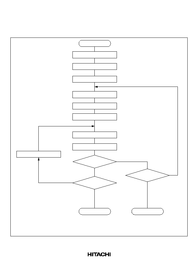
481
High-Speed, High-Reliability Erasing: The H8/3337YF flash memory uses a high-speed, high-
reliability erasing procedure. This procedure provides enhanced erasing speed without subjecting
the device to voltage stress and without sacrificing data reliability . Figure 20.16 shows the basic
high-speed, high-reliability erasing flowchart. Tables 20.15 and 20.16 list the electrical
characteristics during erasing.
Start
Program all bits to 0
*
Address = 0
n = 0
Wait (10 ms)
Erase setup/erase command
n + 1
n
Erase-verify command
Wait (6
µ
s)
Address + 1
address
Verification?
Last address?
End
Fail
n = 3000?
No go
No
Yes
Go
Yes
No
Follow the high-speed, high-reliability programming flowchart in programming all bits. If some bits
are already programmed to 0, program only the bits that have not yet been programmed.
Note:
*
Figure 20.16 High-Speed, High-Reliability Erasing

482
Table 20.15
DC Characteristics in Writer Mode
(Conditions: V
CC
= 5.0 V ±10%, V
PP
= 12.0 V ±0.6 V, V
SS
= 0 V, T
a
= 25∞C ±5∞C)
Item
Symbol
Min
Typ
Max
Unit
Test Conditions
Input high
voltage
FO
7
to FO
0
,
FA
16
to FA
0
,
OE
,
CE
,
WE
V
IH
2.2
--
V
CC
+ 0.3
V
Input low
voltage
FO
7
to FO
0
,
FA
16
to FA
0
,
OE
,
CE
,
WE
V
IL
≠0.3
--
0.8
V
Output high
voltage
FO
7
to FO
0
V
OH
2.4
--
--
V
I
OH
= ≠200 µA
Output low
voltage
FO
7
to FO
0
V
OL
--
--
0.45
V
I
OL
= 1.6 mA
Input leakage
current
FO
7
to FO
0
,
FA
16
to FA
0
,
OE
,
CE
,
WE
| I
LI
|
--
--
2
µA
Vin = 0 to V
CC
V
CC
current
Read
I
CC
--
40
80
mA
Program
I
CC
--
40
80
mA
Erase
I
CC
--
40
80
mA
FV
PP
current
Read
I
PP
--
--
10
µA
V
PP
= 5.0 V
--
10
20
mA
V
PP
= 12.6 V
Program
I
PP
--
20
40
mA
V
PP
= 12.6 V
Erase
I
PP
--
20
40
mA
V
PP
= 12.6 V

483
Table 20.16
AC Characteristics in Writer Mode
(Conditions: V
CC
= 5.0 V ±10%, V
PP
= 12.0 V ±0.6 V, V
SS
= 0 V, T
a
= 25∞C ±5∞C)
Item
Symbol
Min
Typ
Max
Unit
Test Conditions
Command write cycle
t
CWC
120
--
--
ns
Figure 20.17
Address setup time
t
AS
0
--
--
ns
Figure 20.18
*
Address hold time
t
AH
60
--
--
ns
Figure 20.19
Data setup time
t
DS
50
--
--
ns
Data hold time
t
DH
10
--
--
ns
CE
setup time
t
CES
0
--
--
ns
CE
hold time
t
CEH
0
--
--
ns
V
PP
setup time
t
VPS
100
--
--
ns
V
PP
hold time
t
VPH
100
--
--
ns
WE
programming pulse widtht
WEP
70
--
--
ns
WE
programming pulse high time
t
WEH
40
--
--
ns
OE
setup time before command write
t
OEWS
0
--
--
ns
OE
setup time before verify
t
OERS
6
--
--
µs
Verify access time
t
VA
--
--
500
ns
OE
setup time before status polling
t
OEPS
120
--
--
ns
Status polling access time
t
SPA
--
--
120
ns
Program wait time
t
PPW
25
--
--
ns
Erase wait time
t
ET
9
--
11
ms
Output disable time
t
DF
0
--
40
ns
Total auto-erase time
t
AET
0.5
--
30
s
Note:
CE
,
OE
, and
WE
should be high during transitions of V
PP
from 5 V to 12 V and from 12 V to
5 V.
*
Input pulse level: 0.45 V to 2.4 V
Input rise time and fall time
10 ns
Timing reference levels: 0.8 V and 2.0 V for input; 0.8 V and 2.0 V for output
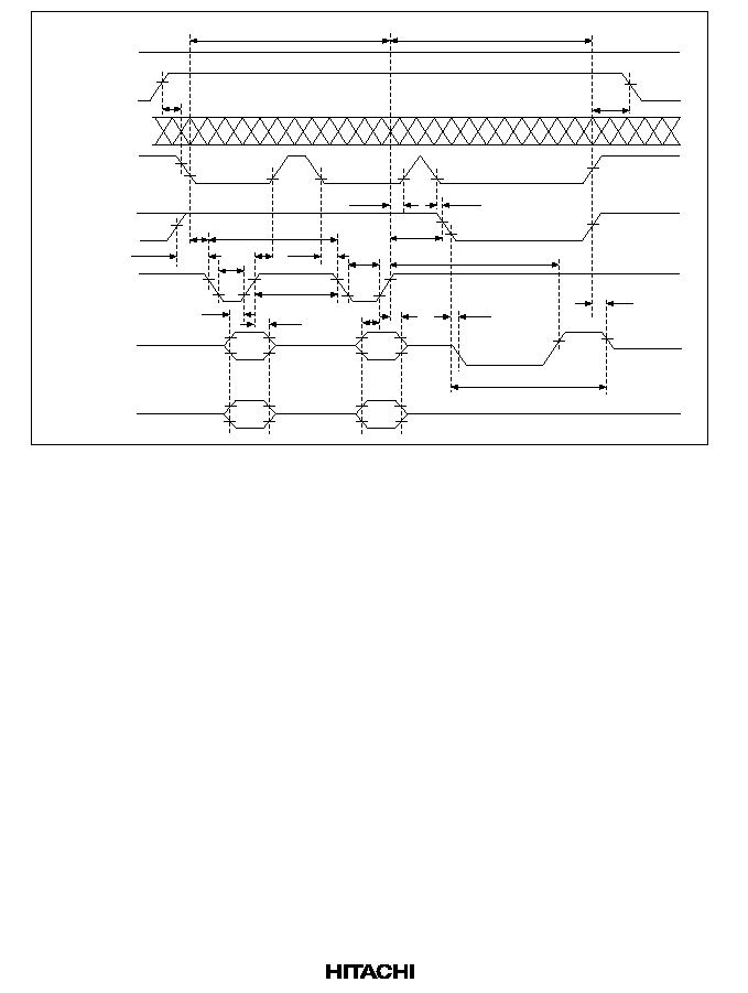
484
Auto-erase setup
Auto-erase and status polling
Address
Command
input
Status polling
Command
input
Command
input
Command
input
5.0 V
12 V
5.0 V
V
CC
V
PP
CE
OE
WE
I/O7
I/O0 to I/O6
t
VPS
t
VPH
t
CEH
t
CES
t
CES
t
OEWS
t
WEP
t
CEH
t
CES
t
CWC
t
WEP
t
OEPS
t
AET
t
WEH
t
DS
t
DH
t
DS
t
DH
t
SPA
t
DF
Figure 20.17 Auto-Erase Timing
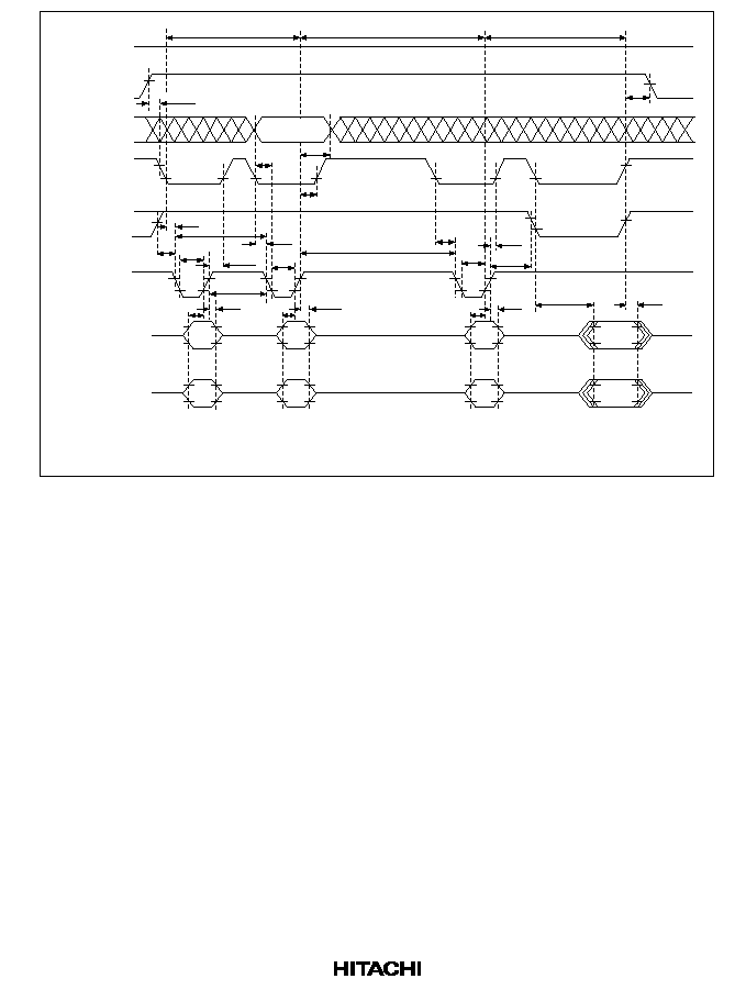
485
t
VPH
t
VPS
t
CEH
t
CES
t
OEWS
t
WEP
t
CEH
t
CES
t
CWC
t
WEP
t
DS
t
DH
t
DS
t
DH
t
AS
t
AH
t
PPW
t
CES
t
WEH
t
CEH
t
WEP
t
OERS
t
DH
t
DS
t
VA
t
DF
Command
input
Command
input
Data
input
Command
input
Command
input
Valid data
output
Data
input
Program setup
Program
Program-verify
Valid address
Address
5.0 V
12 V
5.0 V
V
CC
V
PP
CE
OE
WE
I/O7
I/O0 to I/O6
Note: Program-verify data output values may be intermediate between 1 and 0 before programming has
been completed.
Valid data
output
Figure 20.18 High-Speed, High-Reliability Programming Timing

486
Address
5.0 V
12 V
5.0 V
V
CC
V
PP
CE
OE
WE
I/O0 to I/O7
Erase setup
Erase
Erase-verify
Valid address
Command
input
Command
input
Command
input
Valid data
output
t
VPS
t
VPH
t
AS
t
AH
t
OEWS
t
CWC
t
CES
t
WEP
t
CEH
t
DH
t
DS
t
WEH
t
DS
t
DH
t
DS
t
DH
t
VA
t
DF
t
CES
t
WEP
t
CEH
t
CES
t
ET
t
WEP
t
CEH
t
OERS
Note: Erase-verify data output values may be intermediate between 1 and 0 before erasing has been completed.
Figure 20.19 Erase Timing
20.7
Flash Memory Programming and Erasing Precautions
Read these precautions before using writer mode, on-board programming mode, or flash memory
emulation by RAM.
(1) Program with the specified voltages and timing.
The rated programming voltage (V
PP
) of the flash memory is 12.0 V.
If the PROM programmer is set to Hitachi HN28F101 specifications, V
PP
will be 12.0 V. Applying
voltages in excess of the rating can permanently damage the device. Take particular care to ensure
that the PROM programmer peak overshoot does not exceed the rated limit of 13 V.
(2) Before programming, check that the chip is correctly mounted in the PROM
programmer. Overcurrent damage to the device can result if the index marks on the PROM
programmer socket, socket adapter, and chip are not correctly aligned.
(3) Don't touch the socket adapter or chip while programming. Touching either of these can
cause contact faults and write errors.

487
(4) Set H'FF as the PROM programmer buffer data for addresses H'F780 to H'1FFFF. The
H8/3337YF PROM size is 60 kbytes. Addresses H'F780 to H'1FFFF always read H'FF, so if H'FF
is not specified as programmer data, a verify error will occur.
(5) Notes on applying, releasing, and shutting off
*1
the programming voltage (V
PP
)
∑
Apply the programming voltage (V
PP
) after the rise of V
CC
, and release V
PP
before shutting off
V
CC
.
To prevent unintended programming or erasing of flash memory, in these power-on and
power-off timings, the application, release, and shutting-off of V
PP
must take place when the
microcontroller is in a stable operating condition as defined below.
Stable operating condition
The V
CC
voltage must be stabilized within the rated voltage range (V
CC
= 2.7 V to 5.5 V)
*2
If V
PP
is applied, released, or shut off while the microcontroller's V
CC
voltage is not within
the rated voltage range (V
CC
= 2.7 to 5.5 V)
*2
, since microcontroller operation is unstable,
the flash memory may be programmed or erased by mistake. This can occur even if V
CC
=
0 V. To prevent changes in the V
CC
power supply when V
PP
is applied, be sure that the
power supply is adequately decoupled by inserting bypass capacitors.
Clock oscillation must be stabilized (the oscillation settling time must have elapsed), and
oscillation must not be stopped
When turning on V
CC
power, hold the
RES pin low during the oscillation settling time
(t
OSC1
= 20 ms), and do not apply V
PP
until after this time.
The microcontroller must be in the reset state, or in a state in which a reset has ended
normally (reset has been released) and flash memory is not being accessed
Apply or release V
PP
either in the reset state, or when the CPU is not accessing flash
memory (when a program in on-chip RAM or external memory is executing). Flash
memory cannot be read normally at the instant when V
PP
is applied or released. Do not read
flash memory while V
PP
is being applied or released.
For a reset during operation, apply or release V
PP
only after the
RES pin has been held low
for at least ten system clock cycles (10¯).
The P and E bits must be cleared in the flash memory control register (FLMCR)
When applying or releasing V
PP
, make sure that the P or E bit is not set by mistake.

488
No program runaway
When V
PP
is applied, program execution must be supervised, e.g. by the watchdog timer.
These power-on and power-off timing requirements should also be satisfied in the event of a
power failure and in recovery from a power failure. If these requirements are not satisfied,
overprogramming or overerasing may occur due to program runaway etc., which could cause
memory cells to malfunction.
∑
The V
PP
flag is set and cleared by a threshold decision on the voltage applied to the FV
PP
pin.
The threshold level is between approximately V
CC
+ 2 V to 11.4 V.
When this flag is set, it becomes possible to write to the flash memory control register
(FLMCR) and the erase block registers (EBR1 and EBR2), even though the V
PP
voltage may
not yet have reached the programming voltage range of 12.0 ± 0.6 V.
Do not actually program or erase the flash memory until V
PP
has reached the programming
voltage range.
The programming voltage range for programming and erasing flash memory is 12.0 ± 0.6 V
(11.4 V to 12.6 V). Programming and erasing cannot be performed correctly outside this range.
When not programming or erasing the flash memory, ensure that the V
PP
voltage does not
exceed the V
CC
voltage. This will prevent unintended programming and erasing.
∑
In this chip, the same pin is used for
STBY and FV
PP
. When this pin is driven low, a transition
is made to hardware standby mode. This happens not only in the normal operating modes
(modes 1, 2, and 3), but also when programming the flash memory with a PROM programmer.
When programming with a PROM programmer, therefore, use a programmer which sets this
pin to the V
CC
level when not programming (FV
PP
=12 V).
Notes: *1 Here, V
PP
application, release, and cutoff are defined as follows:
Application:
Raising the voltage from V
CC
to 12±0.6 V.
Release:
Dropping the voltage from 12±0.6 V to V
CC
.
Cutoff:
Halting voltage application (setting the floating state).
*2 In the LH version, V
CC
= 3.0 V to 5.5 V.

489
t
OSC1
2.7 to 5.5 V
*
12
±
0.6 V
V
CC
+ 2 V to 11.4 V
V
CC
V
12
±
0.6 V
V
CC
V
0
µ
s min
0
µ
s min
0
µ
s min
0 to V
CC
V
0 to V
CC
V
Min 10¯
(when
RES
is low)
¯
V
CC
V
PP
V
PP
RES
Boot mode
User program
mode
Timing at which boot
program branches
to RAM area
Periods during which the V
PP
flag is being set or
Note:
*
In the LH version, V
CC
= 3.0 V to 5.5 V.
cleared and flash memory must not be accessed
Figure 20.20 V
PP
Power-On and Power-Off Timing
(6) Do not apply 12 V to the FV
PP
pin during normal operation.
To prevent accidental programming or erasing due to microcontroller program runaway etc., apply
12 V to the V
PP
pin only when the flash memory is programmed or erased, or when flash memory
is emulated by RAM. Overprogramming or overerasing due to program runaway can cause
memory cells to malfunction. Avoid system configurations in which 12 V is always applied to the
FV
PP
pin.
While 12 V is applied, the watchdog timer should be running and enabled to halt runaway
program execution, so that program runaway will not lead to overprogramming or overerasing.
490
(7) Design a current margin into the programming voltage (V
PP
) power supply. Ensure that
V
PP
will not depart from 12.0 ±0.6 V (11.4 V to 12.6 V) during programming or erasing.
Programming and erasing may become impossible outside this range.
(8) Ensure that peak overshoot does not exceed the rated value at the FV
PP
and MD
1
pins.
Connect decoupling capacitors as close to the FV
PP
and MD
1
pins as possible.
Also connect decoupling capacitors to the MD
1
pin in the same way when boot mode is uesd.
0.01
µ
F
1.0
µ
F
12 V
FV
PP
H8/3337YF
Figure 20.21 V
PP
Power Supply Circuit Design (Example)
(9) Use the recommended algorithms for programming and erasing flash memory. These
algorithms are designed to program and erase without subjecting the device to voltage stress and
without sacrificing the reliability of programmed data.
Before setting the program (P) or erase (E) bit in the flash memory control register (FLMCR), set
the watchdog timer to ensure that the P or E bit does not remain set for more than the specified
time.
(10) For details on interrupt handling while flash memory is being programmed or erased,
see the notes on NMI interrupt handling in section 20.4.9, Interrupt Handling during Flash
Memory Programming and Erasing.
(11) Cautions on Accessing Flash Memory Control Registers
1. Flash memory control register access state in each operating mode
The H8/3337YF has flash memory control registers located at addresses H'FF80 (FLMCR),
H'FF82 (EBR1), and H'FF83 (EBR2). These registers can only be accessed when 12 V is
applied to the flash memory program power supply pin, FV
PP
.
Table 1 shows the area accessed for the above addresses in each mode, when 12 V is and is not
applied to FV
PP
.

491
Table 20.17
Area Accessed in Each Mode with 12V Applied and Not Applied to FV
PP
Mode 1
Mode 2
Mode 3
12 V applied to FV
PP
register
Reserved area
(always H'FF)
Flash memory control
register (initial value H'80)
Flash memory control
(initial value H'80)
12 V not applied to
FV
PP
External address
space
External address space
Reserved area (always
H'FF)
2. When a flash memory control register is accessed in mode 2 (expanded mode with on-chip
ROM enabled)
When a flash memory control register is accessed in mode 2, it can be read or written to if
12 V is being applied to FV
PP
, but if not, external address space will be accessed. It is therefore
essential to confirm that 12 V is being applied to the FV
PP
pin before accessing these registers.
3. To check for 12 V application/non-application in mode 3 (single-chip mode)
When address H'FF80 is accessed in mode 3, if 12 V is being applied to FV
PP
, FLMCR is
read/written to, and its initial value after reset is H'80. When 12 V is not being applied to FV
PP
,
FLMCR is a reserved area that cannot be modified and always reads H'FF. Since bit 7
(corresponding to the V
PP
bit) is set to 1 at this time regardless of whether 12 V is applied to
FV
PP
, application or release of 12 V to FV
PP
cannot be determined simply from the 0 or 1 status
of this bit. A byte data comparison is necessary to check whether 12 V is being applied. The
relevant coding is shown below.
.
.
.
LABEL1: MOV.B @H'FF80, R1L
CMP.B #H'FF, R1L
BEQ LABEL1
.
.
.
Sample program for detection of 12 V application to FV
PP
(mode 3)

492
Table 20.18
DC Characteristics of Flash Memory
Conditions: V
CC
= 2.7 V to 5.5 V
*2
, AV
CC
= 2.7 V to 5.5 V
*2
,V
SS
= AV
SS
= 0 V,
V
PP
= 12.0 ± 0.6 V, T
a
= ≠20∞C to +75∞C (regular specifications), T
a
= ≠40∞C to
+85∞C (wide-range specifications)
Item
Symbol
Min
Typ
Max
Unit
Test Conditions
High-voltage
(12 V) threshold
level
*
1
FV
PP
, MD
1
V
H
V
CC
+ 2
--
11.4
V
FV
PP
current
During read
I
PP
--
--
10
µA
V
PP
= 2.7 to 5.5 V
--
10
20
mA
V
PP
= 12.6 V
During
programming
--
20
40
mA
During
erasure
--
20
40
mA
Notes:
*
1 The listed voltages indicate the threshold level at which high-voltage application is
recognized. In boot mode and while flash memory is being programmed or erased, the
applied voltage should be 12.0 V ± 0.6 V.
*
2 In the LH version, V
CC
= 3.0 V to 5.5 V, AV
CC
= 3.0 V to 5.5 V

493
Table 20.19
AC Characteristics of Flash Memory
Conditions: V
CC
= 2.7 V to 5.5 V
*5
, AV
CC
= 2.7 V to 5.5 V
*5
, V
SS
= AV
SS
= 0 V,
V
PP
= 12.0 ± 0.6 V, T
a
= ≠20∞C to +75∞C (regular specifications), T
a
= ≠40∞C to
+85∞C (wide-range specifications)
Item
Symbol
Min
Typ
Max
Unit
Test Conditions
Programming time
*
1,
*
2
t
P
--
50
1000
µs
Erase time
*
1,
*
3
t
E
--
1
30
s
Number of writing/erasing count
N
WEC
--
--
100
Times
Verify setup time 1
*
1
t
VS1
4
--
--
µs
Verify setup time 2
*
1
t
VS2
2
--
--
µs
Flash memory read setup
t
FRS
50
--
--
µs
V
CC
4.5 V
time
*
4
100
--
--
V
CC
< 4.5 V
Notes:
*
1 Set the times following the programming/erasing algorithm shown in section 20.
*
2 The programming time is the time during which a byte is programmed or the P bit in the
flash memory control register (FLMCR) is set. It does not include the program-verify
time.
*
3 The erase time is the time during which all 60-kbyte blocks are erased or the E bit in the
flash memory control register (FLMCR) is set . It does not include the prewrite time
before erasure or erase-verify time.
*
4 After power-on when using an external colck source, after return from standby mode, or
after switching the programming voltage (V
PP
) from 12 V to V
CC
, make sure that this read
setup time has elapsed before reading flash memory.
When V
PP
is released, the flash memory read setup time is defined as the period from
when the FV
PP
pin has reached V
CC
+ 2 V until flash memory can be read.
*
5 In the LH version, V
CC
= 3.0 V to 5.5 V, AV
CC
= 3.0 V to 5.5 V

494

495
Section 21 ROM
(60-kbyte Single-Power-Supply Flash Memory Version)
21.1
Flash Memory Overview
21.1.1
Mode Pin Settings and ROM Space
The H8/3337SF has 60 kbytes of on-chip flash memory. The ROM is connected to the CPU by a
16-bit data bus. The CPU accesses both byte data and word data in two states. Even addresses are
connected to the upper 8 bits, and odd addresses to the lower 8 bits. Word data must start at an
even address.
Enabling and disabling of the on-chip ROM is performed by the mode pins (MD
1
and MD
2
) and
the EXPE bit in MDCR.
The H8/3337SF flash memory can be programmed and erased on-board as well as with a PROM
programmer.
Table 21.1
Mode Pin Settings and ROM Space
Operating Mode
Mode Pin Settings
MCU Operating
Mode
Description
MD
1
MD
0
On-Chip
ROM
Mode 1
Expanded mode with on-chip ROM disabled
0
1
Disabled
Mode 2
Expanded mode with on-chip ROM enabled
1
0
Enabled
Mode 3
Single-chip mode
1
Enabled

496
21.1.2
Features
Features of the flash memory are listed below.
∑
Four flash memory operating modes
The flash memory has four operating modes: program mode, program-verify mode, erase
mode, and erase-verify mode.
∑
Programming and erasing
32 bytes are programmed at a time. Erasing is performed in block units. To erase multiple
blocks, individual blocks must be erased sequentially. In block erasing, 1-kbyte, 28-kbyte, 16-
kbyte, 12-kbyte, and 2-kbyte blocks can be set arbitrarily.
∑
Program and erase times
The flash memory programming time is 10 ms (typ.) for simultaneous 32-byte programming,
equivalent to 300 µs (typ.) per byte, and the erase time for one block is 100 ms (typ.).
∑
Erase-program cycles
Flash memory contents can be erased and reprogrammed up to 100 times.
∑
On-board programming modes
These modes can be used to program, erase, and verify flash memory contents. There are two
modes: boot mode and user programming mode.
∑
Automatic bit rate alignment
In boot-mode data transfer, the H8/3337SF aligns its bit rate automatically to the host bit rate.
∑
Protect modes
There are three modes that enable flash memory to be protected from program, erase, and
verify operations: hardware protect mode, software protect mode, and error protect mode.
∑
Writer mode
As an alternative to on-board programming, the flash memory can be programmed and erased
in writer mode, using a general-purpose PROM programmer.
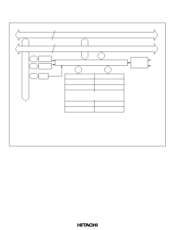
497
21.1.3Block Diagram
Figure 21.1 shows a block diagram of the flash memory.
Internal data bus (lower)
Bus interface and control section
FLMCR1
FLMCR2
EBR2
8
Internal data bus (upper)
8
MD1
MD0
Operating
mode
Upper byte
(even address)
Legend:
FLMCR1: Flash memory control register 1
FLMCR2: Flash memory control register 2
EBR2:
Erase block register 2
On-chip flash memory
(60 kbytes)
H'0000
H'0002
H'0004
H'0001
H'0003
H'0005
H'F77C
H'F77E
H'F77D
H'F77F
Lower byte
(odd address)
Figure 21.1 Flash Memory Block Diagram

498
21.1.4
Input/Output Pins
Flash memory is controlled by the pins listed in table 21.2.
Table 21.2
Flash Memory Pins
Pin Name
Abbreviation
Input/
Output
Function
Reset
RES
Input
Reset
Mode 1
MD
1
Input
H8/3337SF operating mode setting
Mode 0
MD
0
Input
H8/3337SF operating mode setting
Port 92
P9
2
Input
H8/3337SF operating mode setting when MD1 =
MD0 = 0
Port 91
P9
1
Input
H8/3337SF operating mode setting when MD1 =
MD0 = 0
Port 90
P9
0
Input
H8/3337SF operating mode setting when MD1 =
MD0 = 0
Transmit data
TxD
1
Output
SCI1 transmit data output
Receive data
RxD
1
Input
SCI1 receive data input
The transmit data and receive data pins are used in boot mode.
21.1.5
Register Configuration
The flash memory is controlled by the registers listed in table 21.3.
Table 21.3Flash Memory Registers
Name
Abbreviation
R/W
Initial Value
Address
Flash memory control register 1
FLMCR1
R/W
*
2
H'80
H'FF80
Flash memory control register 2
FLMCR2
R/W
*
2
H'00
*
3
H'FF81
Erase block register 2
EBR2
R/W
*
2
H'00
*
3
H'FF83
Wait-state control register
*
1
WSCR
R/W
H'08
H'FFC2
Notes:
*
1 The wait-state control register is used to control the insertion of wait states by the wait-
state controller and frequency division of clock signals for the on-chip supporting
modules by the clock pulse generator. Selection of the respective registers (or
FLMCR1, FLMCR2, and EBR2) is performed by means of the FLSHE bit in the wait
state control register (WSCR).
*
2 In modes in which the on-chip flash memory is disabled, these registers cannot be
modified and return H'00 if read.
*
3 Initialized to H'00 when the SWE bit is not set in FLMCR1.
499
21.1.6
Mode Control Register (MDCR)
Register Configuration: The operating mode of the H8/3337SF is controlled by the mode pins
and the mode control register (MDCR). Table 21.4 shows the MDCR register configuration.
Table 21.4
Register Configuration
Name
Abbreviation
R/W
Initial Value
Address
Mode control register
MDCR
R/W
Undefined
(Depends on operating mode)
H'FFC5
Mode Control Register (MDCR)
Bit
7
6
5
4
3
2
1
0
EXPE
*
1
--
--
--
--
--
MDS1
MDS0
Initial value
--
*
2
1
1
0
0
1
--
*
2
--
*
2
Read/Write
R/W
*
2
--
--
--
--
--
R
R
Notes:
*
1 H8/3337SF (S-mask model, single-power-supply on-chip flash memory version) only.
Otherwise, this is a reserved bit that is always read as 1.
*
2 Determined by the mode pins (MD
1
and MD
0
).
MDCR is an 8-bit register used to set the operating mode of the H8/3337SF and to monitor the
current operating mode.
Bit 7--Expanded Mode Enable (EXPE): Sets expanded mode. In mode 1, this bit is fixed at 1
and cannot be modified. In modes 2 and 3, this bit has a fixed initial value of 0 and cannot be
modified.
This bit can be read and written only in boot mode.
Bit 7: EXPE
Description
0
Single-chip mode is selected
1
Expanded mode is selected (writable in boot mode only)
Bits 6 and 5--Reserved: These bits cannot be modified and are always read as 1.
Bits 4 and 3--Reserved: These bits cannot be modified and are always read as 0.
Bit 2--Reserved: This bit cannot be modified and is always read as 1.
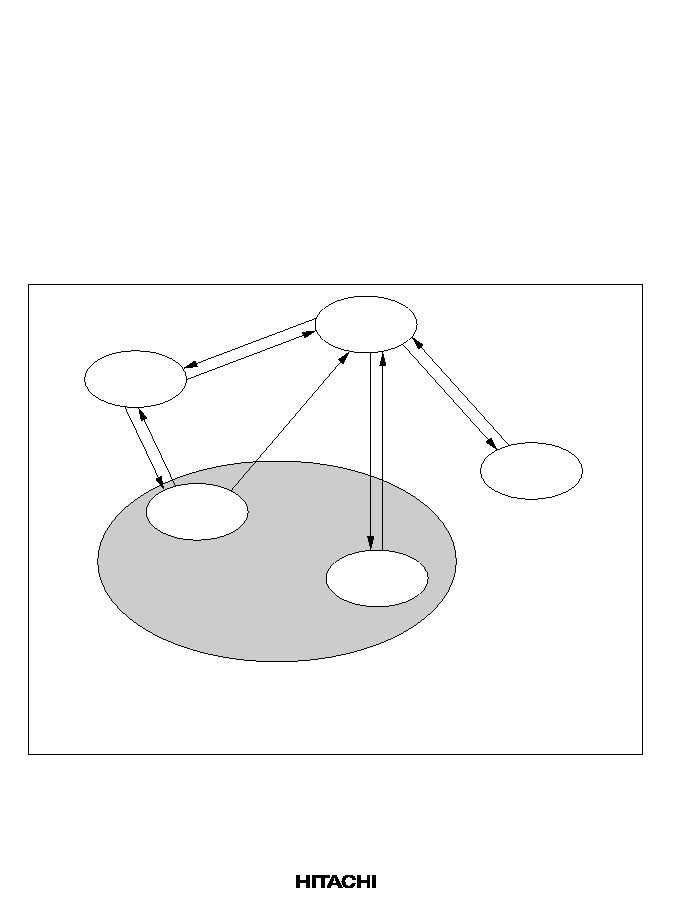
500
Bits 1 and 0--Mode Select 1 and 0 (MDS1, MDS0): These bits indicate the input levels at mode
pins MD
1
and MD
0
(the current operating mode). Bits MDS1 and MDS0 correspond to pins MD
1
and MD
0
, respectively. MDS1 and MDS0 are read-only bits, and cannot be modified. The mode
pin (MD
1
and MD
0
) input levels are latched into these bits when MDCR is read.
21.1.7
Flash Memory Operating Modes
Mode Transition Diagram: When the mode pins are set in the reset state and a reset start is
effected, the microcontroller enters one of the operating modes as shown in figure 21.2. In user
mode, the flash memory can be read but cannot be programmed or erased.
Modes in which the flash memory can be programmed and erased are boot mode, user
programming mode, and writer mode.
Boot mode
On-board programming mode
User
programming
mode
User mode
with on-chip ROM
enabled
Reset state
Writer mode
RES
= 0
FLSHE = 1
FLSHE = 0
*
1
*
2
Notes: Transitions between user mode and user programming mode should only be made when the CPU is
not accessing the flash memory.
*
1 MD
0
= MD
1
= 0, P92 = P91 = P90 = 1
*
2 MD
0
= MD
1
= 0, P92 = 0, P91 = P90 = 1
RES
= 0
RES
= 0
RES
= 0
MD
1
= 1
Figure 21.2 Flash Memory Related State Transitions
501
On-Board Programming Modes
∑
Boot Mode
Flash memory
H8/3337SF
RAM
Host
On-board update routine
SCI
Application
program
(old version)
;;
New application
program
Flash memory
H8/3337SF
RAM
Host
SCI
Application
program
(old version)
New application
program
Flash memory
H8/3337SF
RAM
Host
SCI
Flash memory
erase
Boot program
New application
program
Flash memory
H8/3337SF
:
Program execution state
RAM
Host
SCI
New application
program
Boot program
Boot program area
On-board update routine
;
On-board update routine
;
;
;
;
On-board update
routine
Boot program area
Boot program
Boot program
1. Initial state
The flash memory is in the erased state when
shipped. The procedure for rewriting an old
version of an application program or data is
described here. The user should prepare an
on-board update routine and the new
application program beforehand in the host.
2. SCI communication check
When boot mode is entered, the boot program
in the H8/3337SF (already incorporated in the
chip) is started, an SCI communication check is
carried out, and the boot program required for
flash memory erasing is automatically
transferred to the RAM boot program area.
3. Flash memory initialization
The erase program in the boot program area (in
RAM) is executed, and the flash memory is
initialized (to H'FF). In boot mode, total flash
memory erasure is performed, without regard to
blocks.
4. Writing new application program
The on-board update routine in the host to
RAM is transferred to RAM by SCI
communication and executed, and the new
application program in the host is written into
the flash memory.
Figure 21.3 Boot Mode
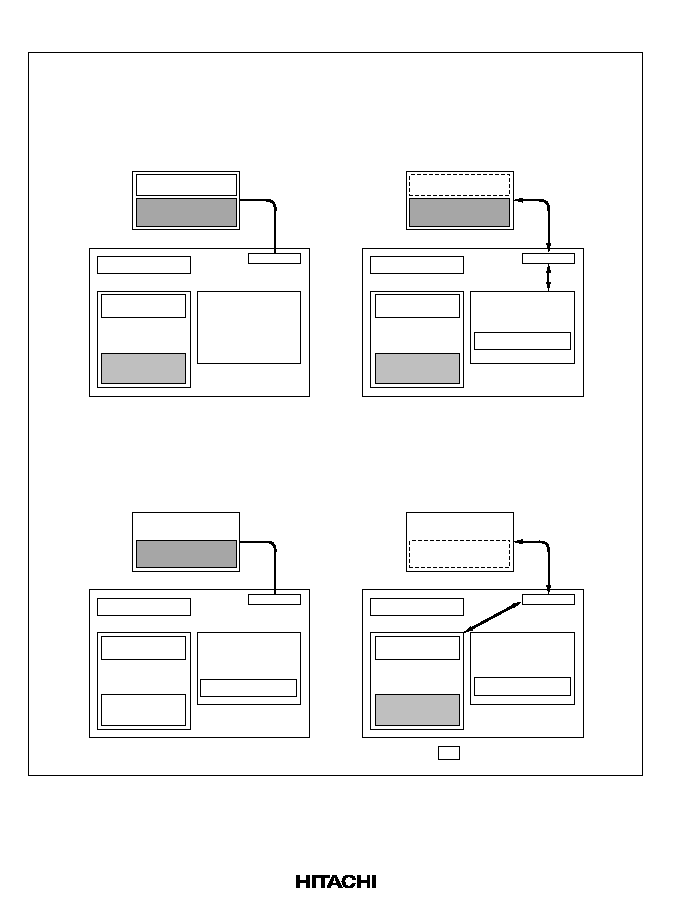
502
∑
User programming mode
Flash memory
H8/3337SF
RAM
Host
On-board update routine
SCI
Boot program
New application
program
Flash memory
H8/3337SF
RAM
Host
SCI
New application
program
Flash memory
H8/3337SF
RAM
Host
SCI
Flash memory
erase
Boot program
New application
program
Flash memory
H8/3337SF
:
Program execution state
RAM
Host
SCI
Boot program
On-board update routine
;
;
Boot program
Transfer program
Application program
(old version)
;
Application program
(old version)
Transfer program
New application
program
Transfer program
;
;
Transfer program
On-board update routine
On-board update routine
1. Initial state
(1) The program that will transfer the on-board
update routine to on-chip RAM should be
written into the flash memory by the user
beforehand. (2) The on-board update routine
should be prepared in the host or in the flash
memory.
2. On-board update routine transfer
The transfer program in the flash memory is
executed, and the on-board update routine is
transferred to RAM.
3. Flash memory initialization
The update routine in RAM is executed, and
the flash memory is initialized (to H'FF).
Erasing can be performed in block units, but
not in byte units.
4. Writing new application program
Next, the new application program in the host is
written into the erased flash memory blocks. Do
not write to unerased blocks.
Figure 21.4 User Programming Mode (Example)
503
Differences between Boot Mode and User Programming Mode
Boot Mode
User Programming Mode
Total erase
Yes
Yes
Block erase
No
Yes
On-board update routine
*
Program/program-verify
Erase/erase-verify
Program/program-verify
Note:
*
To be provided by the user, in accordance with the recommended algorithm.
Block Configuration: The flash memory is divided into one 2-kbyte block, one 12-kbyte block,
one 16-kbyte block, one 28-kbyte block, and four 1-kbyte blocks.
Address H'00000
Address H'F77F
2 kbytes
28 kbytes
16 kbytes
12 kbytes
1 kbyte
1 kbyte
1 kbyte
1 kbyte
60 kbytes
Figure 21.5 Flash Memory Blocks

504
21.2
Flash Memory Register Descriptions
21.2.1
Flash Memory Control Register 1 (FLMCR1)
Bit
7
6
5
4
3
2
1
0
FWE
SWE
--
--
EV
PV
E
P
Initial value
1
0
0
0
0
0
0
0
Read/Write
R
R/W
--
--
R/W
R/W
R/W
R/W
Note:
The FLSHE bit in WSCR must be set to 1 in order for this register to be accessed.
FLMCR1 is an 8-bit register that controls the flash memory operating modes. Program-verify
mode or erase-verify mode is entered by setting SWE to 1. Program mode is entered by setting
SWE to 1 when FWE = 1, then setting the PSU bit in FLMCR2, and finally setting the P bit. Erase
mode is entered by setting SWE to 1, then setting the ESU bit in FLMCR2, and finally setting the
E bit. FLMCR1 is initialized to H'80 by a reset, and in hardware standby mode and software
standby mode. When on-chip flash memory is disabled, a read will return H'00, and writes are
invalid.
Writes to bits EV and PV in FLMCR1 are enabled only when SWE = 1; writes to the E bit only
when FWE = 1, SWE = 1, and ESU = 1; and writes to the P bit only when SWE = 1 and PSU = 1.
Bit 7--Flash Write Enable (FWE): Controls programming and erasing of on-chip flash memory.
In the H8/3337SF, this bit cannot be modified and is always read as 1.
Bit 6--Software Write Enable (SWE): Enables or disables the flash memory. This bit should be
set before setting bits ESU, PSU, EV, PV, E, P, and EB7 to EB0, and should not be cleared at the
same time as these bits.
Bit 6: SWE
Description
0
Writes disabled
(Initial value)
1
Writes enabled
Bits 6 to 4--Reserved: These bits cannot be modified and are always read as 0.

505
Bit 3--Erase-Verify Mode (EV): Selects transition to or exit from erase-verify mode. (Do not set
the SWE, ESU, PSU, PV, E, or P bit at the same time.)
Bit 3: EV
Description
0
Exit from erase-verify mode
(Initial value)
1
Transition to erase-verify mode
[Setting condition]
When SWE = 1
Bit 2--Program-Verify Mode (PV): Selects transition to or exit from program-verify mode. (Do
not set the SWE, ESU, PSU, EV, E, or P bit at the same time.)
Bit 2: PV
Description
0
Exit from program-verify mode
(Initial value)
1
Transition to program-verify mode
[Setting condition]
When SWE = 1
Bit 1--Erase Mode (E): Selects transition to or exit from erase mode. (Do not set the SWE, ESU,
PSU, EV, PV, or P bit at the same time.)
Bit 1: E
Description
0
Exit from erase mode
(Initial value)
1
Transition to erase mode
[Setting condition]
When SWE = 1 and ESU = 1
Bit 0--Program Mode (P): Selects transition to or exit from program mode. (Do not set the
SWE, ESU, PSU, EV, PV, or E bit at the same time.)
Bit 0: P
Description
0
Exit from program mode
(Initial value)
1
Transition to program mode
[Setting condition]
When SWE = 1 and PSU = 1

506
21.2.2
Flash Memory Control Register 2 (FLMCR2)
Bit
7
6
5
4
3
2
1
0
FLER
--
--
--
--
--
ESU
PSU
Initial value
0
0
0
0
0
0
0
0
Read/Write
R
--
--
--
--
--
R/W
R/W
Note:
The FLSHE bit in WSCR must be set to 1 in order for this register to be accessed.
FLMCR2 is an 8-bit register used for monitoring of flash memory program/erase protection (error
protection) and flash memory program/erase mode setup. FLMCR2 is initialized to H'00 by a reset
and in hardware standby mode. The ESU and PSU bits are cleared to 0 in software standby mode,
hardware protect mode, and software protect mode.
When on-chip flash memory is disabled, a read will return H'00.
Bit 7--Flash Memory Error (FLER): Indicates that an error has occurred during an operation on
flash memory (programming or erasing). When FLER is set to 1, flash memory goes to the error-
protection state.
Bit 7: FLER
Description
0
Flash memory is operating normally
Flash memory program/erase protection (error protection) is disabled
[Clearing conditions]
Reset, hardware standby mode, subactive mode, subsleep mode, watch mode
(Initial value)
1
An error occurred during flash memory programming/erasing
Flash memory program/erase protection (error protection) is enabled
[Setting condition]
See Error Protection in section 21.4.5
Bits 6 to 2--Reserved: These bits cannot be modified and are always read as 0.

507
Bit 1--Erase Setup (ESU): Prepares for a transition to erase mode. Set this bit to 1 before setting
the E bit in FLMCR1. (Do not set the SWE, PSU, EV, PV, E, or P bit at the same time.)
Bit 1: ESU
Description
0
Erase setup cleared
(Initial value)
1
Erase setup
[Setting condition]
When SWE = 1
Bit 0--Program Setup (PSU): Prepares for a transition to program mode. Set this bit to 1 before
setting the P bit in FLMCR1. (Do not set the SWE, ESU, EV, PV, E, or P bit at the same time.)
Bit 0: PSU
Description
0
Program setup cleared
(Initial value)
1
Program setup
[Setting condition]
When SWE = 1
21.2.3Erase Block Register 2 (EBR2)
Bit
7
6
5
4
3
2
1
0
EB7
EB6
EB5
EB4
EB3
EB2
EB1
EB0
Initial value
0
0
0
0
1
0
0
0
Read/Write
R/W
*
R/W
R/W
R/W
R/W
R/W
R/W
R/W
Note:
The FLSHE bit in WSCR must be set to 1 in order for this register to be accessed.
*
Writes to bit 7 are invalid in mode 2.
EBR2 is an 8-bit register that designates flash-memory erase blocks for erasure. EBR2 is
initialized to H'00 by a reset, in hardware standby mode and software standby mode, and when the
SWE bit in FLMCR1 is not set. When a bit in EBR2 is set to 1, the corresponding block can be
erased. Other blocks are erase-protected. Only one bit should be set in EBR2; do not set two or
more bits. When on-chip flash memory is disabled, a read will return H'00, and writes are invalid.
The flash memory block configuration is shown in table 21.5.

508
Table 21.5
Flash Memory Erase Blocks
Block (Size)
60-Kbyte Version
Addresses
EB0 (1 kbyte)
H'0000≠H'03FF
EB1 (1 kbyte)
H'0400≠H'07FF
EB2 (1 kbyte)
H'0800≠H'0BFF
EB3 (1 kbyte)
H'0C00≠H'0FFF
EB4 (28 kbytes)
H'1000≠H'7FFF
EB5 (16 kbytes)
H'8000≠H'BFFF
EB6 (12 kbytes)
H'C000≠H'EF7F
EB7 (2 kbytes)
H'EF80≠H'F77F
21.2.4
Wait-State Control Register (WSCR)
Bit
7
6
5
4
3
2
1
0
--
--
CKDBL
FLSHE
WMS1
WMS0
WC1
WC0
Initial value
0
0
0
0
1
0
0
0
Read/Write
R/W
R/W
R/W
R/W
R/W
R/W
R/W
R/W
WSCR is an 8-bit readable/writable register that controls frequency division of the clock signals
supplied to the supporting modules. It also controls wait state controller wait settings, RAM area
setting for dual-power-supply flash memory, and selection/non-selection of single-power-supply
flash memory control registers.
WSCR is initialized to H'08 by a reset and in hardware standby mode. It is not initialized in
software standby mode.
Bits 7 and 6--Reserved: These bits are reserved, but can be written and read. Their initial value
is 0.
Bit 5--Clock Double (CKDBL): Controls frequency division of clock signals supplied to the on-
chip supporting modules. For details, see section 6, Clock Pulse Generator.

509
Bit 4--Flash Memory Control Register Enable (FLSHE): When the FLSHE bit is set to 1, the
flash memory control registers can be read and written to. When FLSHE is cleared to 0, the flash
memory control registers are unselected. In this case, the contents of the flash memory contents
are retained.
Bit 4: FLSHE
Description
0
Flash memory control registers are in unselected state
(Initial value)
1
Flash memory control registers are in selected state
Bits 3 and 2--Wait Mode Select 1 and 0 (WMS1, WMS0)
Bits 1 and 0--Wait Count 1 and 0 (WC1, WC0)
These bits control insertion of wait states by the wait-state controller. For details, see section 5,
Wait-State Controller.
21.3On-Board Programming Modes
When an on-board programming mode is selected, the on-chip flash memory can be programmed,
erased, and verified. There are two on-board programming modes: boot mode and user
programming mode. Table 21.6 indicates how to select the on-board programming modes. User
programming mode operation can be performed by setting control bits with software. A state
transition diagram for flash memory related modes is shown in figure 21.2.
Table 21.6
On-Board Programming Mode Selection
Mode Selection
MD
1
MD
0
P9
2
P9
1
P9
0
Boot mode
0
0
1
1
1
User programming
1
0
--
--
--
mode
1
21.3.1
Boot Mode
To use boot mode, a user program for programming and erasing the flash memory must be
provided in advance on the host machine (which may be a personal computer). Serial
communication interface (SCI) channel 1 is used in asynchronous mode.
When a reset state is executed after the H8/3337SF pins have been set to boot mode, the built-in
boot program is activated, and the on-board update routine provided in the host is transferred
sequentially to the H8/3337SF using the serial communication interface (SCI). The H8/3337SF
writes the on-board update routine received via the SCI to the on-board update routine area in the
on-chip RAM. After the transfer is completed, execution branches to the first address of the on-

510
board update routine area, and the on-board update routine execution state is entered (flash
memory programming is performed).
Therefore, a routine conforming to the programming algorithm described later must be provided in
the on-board update routine transferred from the host.
Figure 21.6 shows the system configuration in boot mode, and figure 21.7 shows the boot mode
execution procedure.
RxD1
TxD1
SCI1
H8/3337SF
Flash memory
Reception of programming data
Transmission of verification data
Host
On-chip RAM
Figure 21.6 Boot-Mode System Configuration
Boot-Mode Execution Procedure: Figure 21.7 shows the boot-mode execution procedure.

511
n = N?
Note: If a memory cell malfunctions and cannot be erased, the H8/3337SF transmits one H'FF byte to report an erase
error, halts erasing, and halts further operations.
Yes
No
Program H8/3337SF pins for boot mode, and
reset
n = 1
n + 1
n
Host transmits H'00 data continuously at desired
bit rate
H8/3337SF measures low period of H'00 data
transmitted from host
After completing bit-rate alignment, H8/3337SF
sends one H'00 data byte to host to indicate that
alignment is completed
Host checks that this byte, indicating completion
of bit-rate alignment, is received normally, then
transmits one H'55 byte.
After receiving H'55, H8/3337SF sends part of
the boot program to RAM
After checking that all data in flash memory has
been erased, H8/3337SF transmits one H'AA
data byte to host
Check flash memory data, and if data has
already been written, erase all blocks
Host transmits user program sequentially,
in byte units
H8/3337SF transmits received user program to
host as verification data (echo-back)
Transfer received on-board update routine to
on-chip RAM
End of transfer
Transmit one H'AA data byte to host, and
execute on-board update routine transferred
to on-chip RAM
Host transmits byte length (N) of user program in
two bytes, upper byte followed by lower byte
H8/3337SF transmits received byte length to
host as verification data (echo-back)
Start
H8/3337SF computes bit rate and sets bit rate
register
Figure 21.7 Boot Mode Flowchart

512
Automatic Alignment of SCI Bit Rate
Start
bit
D0
D1
D2
D3
D4
D5
D6
D7
Stop
bit
This low period (9 bits) is measured (H'00 data)
High for at
least 1 bit
Figure 21.8 Measurement of Low Period in Data Transmitted from Host
When started in boot mode, the H8/3337SF measures the low period in asynchronous SCI data
(H'00) transmitted from the host. The data format is eight data bits, one stop bit, and no parity bit.
From the measured low period (9 bits), the H8/3337SF computes the host's bit rate. After aligning
its own bit rate, the H8/3337SF sends the host one byte of H'00 data to indicate that bit-rate
alignment is completed. The host should check that this alignment-completed indication is
received normally and send one H'55 byte back to the H8/3337SF. If the alignment-completed
indication is not received normally, the H8/3337F should be reset, then restarted in boot mode to
measure the low period again. There may be some alignment error between the host's and
H8/3337SF's bit rates, depending on the host's transmission bit rate and the H8/3337SF's system
clock frequency (f
OSC
). To have the SCI operate normally, set the host's transfer bit rate to 2400,
4800, or 9600 bps.
Table 21.7 lists typical host transfer bit rates and indicates the system clock frequency ranges over
which the H8/3337SF can align its bit rate automatically. Boot mode should be used within these
frequency ranges.
Table 21.7
System Clock Frequencies Permitting Automatic Bit-Rate Alignment by
H8/3337SF
Host Bit Rate
System Clock Frequencies (f
OSC
) Permitting Automatic Bit-Rate
Alignment by H8/3337SF
9600 bps
8 MHz to 16 MHz
4800 bps
4 MHz to 16 MHz
2400 bps
2 MHz to 16 MHz
RAM Area Allocation in Boot Mode: In boot mode, the 128 bytes from H'FF00 to H'FF7F are
reserved for use by the boot program, as shown in figure 21.9. The user program is transferred into
the area from H'F780 to H'FDFF (1664 bytes). The boot program area can be used after the
transition to execution of the user program transferred into RAM. If a stack area is needed, set it
within the user program.

513
H'FF00
H'FF7F
H'F780
Boot program
area
*
(128 bytes)
User program
transfer area
(1664 bytes)
H'FDFF
Note:
*
This area cannot be used until the H8/3337SF starts to execute the user program
transferred to RAM. Note that even after the branch to the user program, the boot
program area still contains the boot program.
Figure 21.9 RAM Areas in Boot Mode
Notes on Use of Boot Mode
1. When the H8/3337SF comes out of reset in boot mode, it measures the low period of the input
at the SCI's RxD
1
pin. The reset should end with RxD
1
high. After the reset ends, it takes about
100 states for the H8/3337SF to get ready to measure the low period of the RxD
1
input.
2. In boot mode, if any data has been programmed into the flash memory (if all data is not H'FF),
all flash memory blocks are erased. Boot mode is for use when user programming mode is
unavailable, such as the first time on-board programming is performed, or if the program
activated in user programming mode is accidentally erased.
3. Interrupts cannot be used while the flash memory is being programmed or erased.
4. The RxD
1
and TxD
1
pins should be pulled up on-board.
5. Before branching to the user program (at address H'E880 in the RAM area), the H8/3337SF
terminates transmit and receive operations by the on-chip SCI (by clearing the RE and TE bits
of serial control register SCR to 0 in channel 1), but the auto-aligned bit rate remains set in bit
rate register BRR. The transmit data output pin (TxD
1
) is in the high output state (in port 8, bits
P8
4
DDR of the port 8 data direction register and P8
4
DR of the port 8 data register are set to 1).
514
At this time, the values of general registers in the CPU are undetermined. Thus these registers
should be initialized immediately after branching to the user program. Especially in the case of
the stack pointer (SP), which is used implicitly in subroutine calls, etc., the stack area used by
the user program should be specified.
There are no other changes to the initialized values of other registers.
6. Boot mode can be entered by starting from a reset after pin settings are made according to the
mode setting conditions listed in table 21.6.
In the H8/3337SF, P9
2
, P9
1
, and P9
0
can be used as I/O ports if boot mode selection is detected
when reset is released
*1
.
Boot mode can be released by driving the reset pin low, waiting at least 20 system clock
cycles, then setting the mode pins and releasing the reset
*1
.
Boot mode can also be released if a watchdog timer overflow reset occurs.
The mode pin input levels must not be changed during boot mode.
7. If the input level of a mode pin is changed during a reset (e.g., from low to high), the resultant
switch in the microcontroller's operating mode will affect the bus control output signals (
AS,
RD, and WR) and the status of ports that can be used for address output
*2
.
Therefore, either set these pins so that they do not output signals during the reset, or make sure
that their output signals do not collide with other signals output the microcontroller.
Notes: *1 Mode pin input must satisfy the mode programming setup time (t
MDS
= 4 states) with
respect to the reset release timing.
*2 These ports output low-level address signals if the mode pins are set to mode 1 during
the reset. In all other modes, these ports are in the high-impedance state. The bus
control output signals are high if the mode pins are set for mode 1 or 2 during the reset.
In mode 3, they are at high impedance.
RES
MD
0,
MD
1
P9
2
P9
1
P9
0
tMDS
tMDS: 4t
CYC
(min.)
Figure 21.10 Programming Mode Timing
515
21.3.2
User Programming Mode
When set to user programming mode, the H8/3337SF can erase and program its flash memory by
executing a user program. On-board updates of the on-chip flash memory can be carried out by
providing an on-board circuit for supplying programming data, and storing an update program in
part of the program area.
To select user programming mode, start up in a mode that enables the on-chip flash memory
(mode 2 or 3). In user programming mode, the on-chip supporting modules operate as they
normally would in mode 2 or 3, except for the flash memory.
The flash memory cannot be read while the SWE bit is set to 1 in order to perform programming
or erasing, so the update program must be executed in on-chip RAM or external memory.
User Programming Mode Execution Procedure (Example): Figure 21.11 shows the execution
procedure for user programming mode when the on-board update routine is executed in RAM.
Branch to flash memory on-board
update routine in RAM
Execute flash memory on-board
update routine (update flash memory)
Branch to application program
in flash memory
The transfer program (and on-board update
program as required) is written in flash
memory ahead of time by the user.
Note: Start the watchdog timer to prevent over-erasing due to program runaway, etc.
Transfer on-board update routine
into RAM
Set MD
1
and MD
0
to 10 or 11
Start from reset
Figure 21.11 User Programming Mode Operation (Example)

516
21.4
Programming/Erasing Flash Memory
In the on-board programming modes, flash memory programming and erasing is performed by
software, using the CPU. There are four flash memory operating modes: program mode, erase
mode, program-verify mode, and erase-verify mode. Transitions to these modes can be made by
setting the PSU and ESU bits in FLMCR2, and the P, E, PV, and EV bits in FLMCR1.
The flash memory cannot be read while being programmed or erased. Therefore, the program that
controls flash memory programming/erasing (the programming control program) should be
located and executed in on-chip RAM or external memory.
Notes: 1. Operation is not guaranteed if setting/resetting of the SWE, EV, PV, E, and P bits in
FLMCR1, and the ESU and PSU bits in FLMCR2, is executed by a program in flash
memory.
2. Perform programming in the erased state. Do not perform additional programming on
previously programmed addresses.
21.4.1
Program Mode
Follow the procedure shown in the program/program-verify flowchart in figure 21.12 to write data
or programs to flash memory. Performing program operations according to this flowchart will
enable data or programs to be written to flash memory without subjecting the device to voltage
stress or sacrificing program data reliability. Programming should be carried out 32 bytes at a
time.
For the wait times (x, y, z,
,
,
, , )
after setting/clearing individual bits in flash memory
control registers 1 and 2 (FLMCR1, FLMCR2) and the maximum number of writes (N), see Flash
Memory Characteristics in section 23, Electrical Characteristics.
Following the elapse of (x) µs or more after the SWE bit is set to 1 in flash memory control
register 1 (FLMCR1), 32-byte program data is stored in the program data area and reprogram data
area, and the 32-byte data in the reprogram data area written consecutively to the write addresses.
The lower 8 bits of the first address written to must be H'00, H'20, H'40, H'60, H'80, H'A0, H'C0,
or H'E0. Thirty-two consecutive byte data transfers are performed. The program address and
program data are latched in the flash memory. A 32-byte data transfer must be performed even if
writing fewer than 32 bytes; in this case, H'FF data must be written to the extra addresses.
Next, the watchdog timer is set to prevent overprogramming in the event of program runaway, etc.
Set a value greater than (y + z +
+
) µs as the WDT overflow period. After this, preparation for
program mode (program setup) is carried out by setting the PSU bit in FLMCR2, and after the
elapse of (y) µs or more, the operating mode is switched to program mode by setting the P bit in
FLMCR1. The time during which the P bit is set is the flash memory programming time. Make a
program setting so that the time for one programming operation is within the range of (z) µs.

517
21.4.2
Program-Verify Mode
In program-verify mode, the data written in program mode is read to check whether it has been
correctly written in the flash memory.
After the elapse of a given programming time, the programming mode is exited (the P bit in
FLMCR1 is cleared, then the PSU bit in FLMCR2 is cleared at least (
) µs later). The watchdog
timer is cleared after the elapse of (
) µs or more, and the operating mode is switched to program-
verify mode by setting the PV bit in FLMCR1. Before reading in program-verify mode, a dummy
write of H'FF data should be made to the addresses to be read. The dummy write should be
executed after the elapse of (
) µs or more. When the flash memory is read in this state (verify data
is read in 16-bit units), the data at the latched address is read. Wait at least (
) µs after the dummy
write before performing this read operation. Next, the originally written data is compared with the
verify data, and a bit generation operation is performed for reprogram data (see figure 21.12) and
transferred to the reprogram data area. After 32 bytes of data have been verified, exit program-
verify mode, wait for at least (
) µs, then clear the SWE bit in FLMCR1. If reprogramming is
necessary, set program mode again, and repeat the program/program-verify sequence as before.
However, ensure that the program/program-verify sequence is not repeated more than (N) times on
the same bits.

518
Set SWE bit in FLMCR1
Wait (x)
µ
s
n = 1
m = 0
Write 32-byte data in RAM reprogram data
area consecutively to flash memory
Enable WDT
Set PSU bit in FLMCR2
Wait (y)
µ
s
Set P bit in FLMCR1
Wait (z)
µ
s
Start of programming
Clear P bit in FLMCR1
Wait (
)
µ
s
Wait (
)
µ
s
NG
NG
NG
NG
OK
OK
OK
Wait (
)
µ
s
Wait (
)
µ
s
*
5
*
3
*
4
*
2
*
5
*
5
*
5
*
5
*
5
*
5
*
5
Store 32-byte program data in program
data area and reprogram data area
*
4
*
1
*
5
Wait (
)
µ
s
Clear PSU bit in FLMCR2
Disable WDT
Set PV bit in FLMCR1
H'FF dummy write to verify address
Read verify data
Reprogram data computation
Clear PV bit in FLMCR1
Clear SWE bit in FLMCR1
m = 1
End of programming
Program data =
verify data?
End of 32-byte
data verification?
m = 0?
Increment address
Programming failure
OK
Clear SWE bit in FLMCR1
n
N?
n
n + 1
Notes:
*
1 Data transfer is performed by byte transfer. The lower
8 bits of the first address written to must be H'00, H'20, H'40,
H'60, H'80, H'A0, H'C0, or H'E0. A 32-byte data transfer
must be performed even if writing fewer than 32 bytes;
in this case, H'FF data must be written to the extra addresses.
*
2 Verify data is read in 16-bit (word) units.
*
3 If a bit for which programming has been completed in the 32-byte
programming loop fails the following verify phase, additional
programming is performed for that bit.
*
4 An area for storing program data (32 bytes) and reprogram data
(32 bytes) must be provided in RAM. The contents of the latter
are rewritten as programming progresses.
*
5 See section 23, Flash Memory Characteristics, for the values of
x, y, z,
,
,
,
,
, and N.
Start
Program
Data
Reprogram
Data
Comments
Reprogramming is not
performed if program data
and verify data match
Programming incomplete;
reprogram
--
Still in erased state;
no action
RAM
Program data storage
area (32 bytes)
Reprogram data storage
area (32 bytes)
Transfer reprogram data to reprogram
data area
Verify
Data
1
0
1
1
0
1
0
1
0
0
1
1
End of programming
Perform programming in the erased state.
Do not perform additional programming
on previously programmed addresses.
Figure 21.12 Program/Program-Verify Flowchart

519
21.4.3Erase Mode
Flash memory erasing should be performed block by block following the procedure shown in the
erase/erase-verify flowchart (single-block erase) shown in figure 21.13.
The wait times (x, y, z,
,
,
, , )
after setting/clearing individual bits in flash memory control
registers 1 and 2 (FLMCR1, FLMCR2) and the maximum number of erases (N), see Flash
Memory Characteristics in section 23, Electrical Characteristics.
To perform data or program erasure, make a 1 bit setting for the flash memory area to be erased in
erase block register 2 (EBR2) at least (x) µs after setting the SWE bit to 1 in flash memory control
register 1 (FLMCR1). Next, the watchdog timer is set to prevent overerasing in the event of
program runaway, etc. Set a value greater than (y + z +
+
) ms as the WDT overflow period.
After this, preparation for erase mode (erase setup) is carried out by setting the ESU bit in
FLMCR2, and after the elapse of (y) µs or more, the operating mode is switched to erase mode by
setting the E bit in FLMCR1. The time during which the E bit is set is the flash memory erase
time. Ensure that the erase time does not exceed (z) ms.
Note:
With flash memory erasing, preprogramming (setting all data in the memory to be erased
to 0) is not necessary before starting the erase procedure.
21.4.4
Erase-Verify Mode
In erase-verify mode, data is read after memory has been erased to check whether it has been
correctly erased.
After the elapse of the erase time, erase mode is exited (the E bit in FLMCR1 is cleared, then the
ESU bit in FLMCR2 is cleared at least (
) µs later), the watchdog timer is cleared after the elapse
of (
) µs or more, and the operating mode is switched to erase-verify mode by setting the EV bit
in FLMCR1. Before reading in erase-verify mode, a dummy write of H'FF data should be made to
the addresses to be read. The dummy write should be executed after the elapse of (
) µs or more.
When the flash memory is read in this state (verify data is read in 16-bit units), the data at the
latched address is read. Wait at least (
) µs after the dummy write before performing this read
operation. If the read data has been erased (all 1), a dummy write is performed to the next address,
and erase-verify is performed. If the read data has not been erased, set erase mode again, and
repeat the erase/erase-verify sequence in the same way. However, ensure that the erase/erase-
verify sequence is not repeated more than (N) times. When verification is completed, exit erase-
verify mode, and wait for at least (
) µs. If erasure has been completed on all the erase blocks,
clear the SWE bit in FLMCR1. If there are any unerased blocks, make a 1 bit setting in EBR2 for
the flash memory area to be erased, and repeat the erase/erase-verify sequence in the same way.
520
End of erasing
Start
Set SWE bit in FLMCR1
Set ESU bit in FLMCR2
Set E bit in FLMCR1
Wait (x)
µ
s
Wait (y)
µ
s
n = 1
Set EBR1, EBR2
Enable WDT
*
5
*
5
*
3
Wait (z) ms
*
5
Wait (
)
µ
s
*
5
Wait (
)
µ
s
*
5
Wait (
)
µ
s
Set block start address to verify address
*
5
Wait (
)
µ
s
*
5
*
2
*
5
Wait (
)
µ
s
*
5
*
5
*
4
Start of erase
Clear E bit in FLMCR1
Clear ESU bit in FLMCR2
Set EV bit in FLMCR1
H'FF dummy write to verify address
Read verify data
Clear EV bit in FLMCR1
Wait (
)
µ
s
Clear EV bit in FLMCR1
Clear SWE bit in FLMCR1
Disable WDT
Halt erase
*
1
Verify data = all 1?
Last address of block?
End of
erasing of all erase
blocks?
Erase failure
Clear SWE bit in FLMCR1
n
N?
NG
NG
NG
NG
OK
OK
OK
OK
n
n + 1
Increment
address
Notes:
*
1 Preprogramming (setting erase block data to all 0) is not necessary.
*
2 Verify data is read in 16-bit (W) units.
*
3 Set only one bit in EBR2. More than one bit cannot be set.
*
4 Erasing is performed in block units. To erase a number of blocks, the individual blocks must be erased sequentially.
*
5 See section 23, Electrical Characteristics, Flash Memory Characteristics, for the values of x, y, z,
,
,
,
,
, and N.
Figure 21.13 Erase/Erase-Verify Flowchart (Single-Block Erase)

521
21.4.5
Protect Modes
There are three modes for protecting flash memory from programming and erasing: software
protection, hardware protection, and error protection. These protection modes are described below.
Software Protection: Software protection can be implemented by setting the SWE bit in flash
memory control register 1 (FLMCR1), and setting erase block register 2 (EBR2). Software
protection prevents transitions to program mode and erase mode even if the P or E bit is set in
FLMCR1.
Details of software protection are shown in table 21.8.
Table 21.8
Software Protection
Functions
Item
Description
Program
Erase
SWE bit protect
Clearing the SWE bit to 0 in FLMCR1 sets the
program/erase-protected state for all blocks.
(Execute in on-chip RAM or external memory.)
Yes
Yes
Block protect
Individual blocks can be protected from erasing
and programming by erase block register 2
(EBR2). If H'00 is set in EBR2, all blocks are
protected from erasing and programming.
--
Yes
Hardware Protection: Hardware protection refers to a state in which programming and erasing of
flash memory is forcibly suspended or disabled. At this time, the flash memory control registers 1
and 2 (FLMCR1, FLMCR2) and erase block register 2 (EBR2) settings are reset.
Details of hardware protection are shown in table 21.9.
Table 21.9
Hardware Protection
Functions
Item
Description
Program
Erase
Reset and
standby protect
When a reset occurs (including a watchdog timer
reset) or standby mode is entered, FLMCR1,
FLMCR2, and EBR2 are initialized, disabling
programming and erasing. Note that
RES
input
does not ensure a reset unless the
RES
pin is
held low until the oscillator settles at power-up, or
for a period equivalent to the
RES
pulse width
specified in the AC characteristics during
operation.
Yes
Yes

522
Error Protection: In error protection, an error is detected when microcontroller runaway occurs
during flash memory programming/erasing, or operation is not performed in accordance with the
program/erase algorithm, and the program/erase operation is aborted. Aborting the program/erase
operation prevents damage to the flash memory due to overprogramming or overerasing.
If the microcontroller malfunctions during flash memory programming/erasing, the FLER bit is set
to 1 in FLMCR2 and the error protection state is entered. The FLMCR1, FLMCR2, and EBR2
settings are retained, but program mode or erase mode is aborted at the point at which the error
occurred. Program mode or erase mode cannot be re-entered by re-setting the P or E bit. However,
PV and EV bit setting is enabled, and a transition can be made to verify mode.
FLER bit setting conditions are as follows:
1. When flash memory is read during programming/erasing (including a vector read or instruction
fetch)
2. Immediately after the start of exception handling (excluding a reset) during
programming/erasing
3. When a SLEEP instruction (including software standby) is executed during
programming/erasing
4. When the bus is released during programming/erasing
Error protection is released only by a power-on reset.
Figure 21.14 shows the flash memory state transition diagram.
523
RD
VF
PR ER FLER = 0
Error occurrence
RES
= 0 or
STBY
= 0
RES
= 0 or
STBY
= 0
RD
VF
PR
ER
FLER = 0
Program mode
Erase mode
Reset or
hardware standby
(hardware protection)
RD VF
PR
ER
FLER = 1
RD
VF
PR
ER
FLER = 1
Error protect mode
Error protect mode
(standby)
Software standby mode
FLMCR1, FLMCR2 (except FLER bit),
EBR2 initialized
FLMCR1, FLMCR2,
EBR2 initialized
Software standby mode
release
RD: Memory read possible
RD
: Memory read not possible
VF: Verify-read possible
VF
: Verify-read not possible
PR: Programming possible
PR
: Programming not possible
ER: Erasing possible
ER
: Erasing not possible
RES
= 0 or
STBY
= 0
Error occurrence
(software standby
mode)
Figure 21.14 Flash Memory State Transitions
21.4.6
Interrupt Handling during Flash Memory Programming and Erasing
All interrupts, including NMI input, should be disabled when flash memory is being programmed
or erased (while the P or E bit is set in FLMCR1) and while the boot program is executing in boot
mode
*1
, to give priority to the program or erase operation. There are three reasons for this:
1. Interrupt occurrence during programming or erasing might cause a violation of the
programming or erasing algorithm, with the result that normal operation could not be assured.
2. In the interrupt exception handling sequence during programming or erasing, the vector would
not be read correctly
*2
, possibly resulting in microcontroller runaway.
3. If an interrupt occurred during boot program execution, it would not be possible to execute the
normal boot mode sequence.
For these reasons, there are conditions for disabling interrupts in the on-board programming
modes alone, as an exception to the general rule. However, this provision does not guarantee
normal erasing and programming or microcontroller operation.
All requests, including NMI, must therefore be disabled inside and outside the microcontroller
when flash memory is programmed or erased. Interrupts are also disabled in the error protection
state while the P or E bit setting in FLMCR1 is held.

524
Notes: *1 Interrupt requests must be disabled inside and outside the microcontroller until
programming by the update program has been completed.
*2 The vector may not be read correctly in this case for the following two reasons:
∑ If flash memory is read while being programmed or erased (while the P or E bit is
set in FLMCR1), correct read data will not be obtained (undetermined values will be
returned).
∑ If a value has not yet been written in the interrupt vector table, interrupt exception
handling will not be executed correctly.
21.5
Flash Memory Writer Mode (H8/3337SF)
21.5.1
Writer Mode Setting
Programs and data can be written and erased in writer mode as well as in the on-board
programming modes. In writer mode, the on-chip ROM can be freely programmed using a PROM
programmer that supports the Hitachi microcomputer device type* with 64-kbyte on-chip flash
memory*. Flash memory read mode, auto-program mode, auto-erase mode, and status read mode
are supported with this device type. In auto-program mode, auto-erase mode, and status read
mode, a status polling procedure is used, and in status read mode, detailed internal signals are
output after execution of an auto-program or auto-erase operation.
Note: * The H8/3437 should be used with the PROM programmer programming voltage set to
5.0 V.
Table 21.10
Writer Mode Pin Settings
Pin Names
Settings
Mode pins: MD
1
, MD
0
Low level input to MD
1
and MD
0
STBY
pin
High level input (hardware standby mode not entered)
RES
pin
Power-on reset circuit
XTAL and EXTAL pins
Oscillator circuit
Other setting pins: P9
7
, P9
2
, P9
1
, P9
0
, P6
7
Low level input to P9
2
and P6
7
, high level input to P9
7
,
P9
1
, and P9
0
21.5.2
Socket Adapter and Memory Map
In writer mode, a socket adapter for the relevant kind of package is attached to the PROM
programmer. Socket adapters are available for all PROM programmer manufacturers supporting
the Hitachi microcomputer device type with 64-kbyte on-chip flash memory.

525
Figure 21.15 shows the memory map in writer mode, and table 21.10 shows writer mode pin
settings. For pin names in writer mode, see section 1.3.2, Pin Functions in Each Operating Mode.
On-chip ROM area
H8/3337SF
Writer mode
H'0000
H'F77F
H'0000
H'F77F
H'1FFFF
MCU mode
Undetermined values
output
Figure 21.15 Memory Map in Writer Mode
21.5.3Operation in Writer Mode
Table 21.11 shows how to select the various operating modes when using writer mode, and table
21.12 lists the commands used in writer mode. Details of each mode are given below.
∑
Memory Read Mode
Memory read mode supports byte reads.
∑
Auto-Program Mode
Auto-program mode supports programming of 128 bytes at a time. Status polling is used to
confirm the end of auto-programming.
∑
Auto-Erase Mode
Auto-erase mode supports automatic erasing of the entire flash memory. Status polling is used
to confirm the end of auto-erasing.
∑
Status Read Mode
Status polling is used for auto-programming and auto-erasing, and normal termination can be
confirmed by reading the FO6 signal. In status read mode, error information is output if an
error occurs.

526
Table 21.11
Operating Mode Selection in Writer Mode
Pins
Mode
CE
OE
WE
FO7≠FO0
FA17≠FA0
Read
L
L
H
Data output
Ain
*
2
Output disable
L
H
H
High impedance
X
Command write
L
H
L
Data input
Ain
*
2
Chip disable
*
1
H
X
X
High impedance
X
Notes:
*
1 Chip disable is not a standby state; internally, it is an operation state.
*
2 Ain indicates that there is also address input in auto-program mode.
Table 21.12
Writer Mode Commands
1st Cycle
2nd Cycle
Command
Cycles
Mode
Address
Data
Mode
Address
Data
Memory read mode
1 + n
Write
X
H'00
Read
RA
Dout
Auto-program mode
129
Write
X
H'40
Write
WA
Din
Auto-erase mode
2
Write
X
H'20
Write
X
H'20
Status read mode
2
Write
X
H'71
Write
X
H'71
Notes: 1. In auto-program mode, 129 cycles are required for command writing by a simultaneous
128-byte write.
2. In memory read mode, the number of cycles depends on the number of address write
cycles (n).
527
Memory Read Mode
1. After completion of auto-program/auto-erase/status read operations, a transition is made to the
command wait state. When reading memory contents, a transition to memory read mode must
first be made with a command write, after which the memory contents are read.
2. In memory read mode, command writes can be performed in the same way as in the command
wait state.
3. Once memory read mode has been entered, consecutive reads can be performed.
4. After powering up, memory read mode is entered.
Table 21.13AC Characteristics in Memory Read Mode
(Conditions: V
CC
= 5.0 V ±10%, V
SS
= 0 V, T
a
= 25∞C ±5∞C)
Item
Symbol
Min
Max
Unit
Notes
Command write cycle
t
nxtc
20
µ
s
CE
hold time
t
ceh
0
ns
CE
setup time
t
ces
0
ns
Data hold time
t
dh
50
ns
Data setup time
t
ds
50
ns
Programming pulse width
t
wep
70
ns
WE
rise time
t
r
30
ns
WE
fall time
t
f
30
ns
CE
Address
Data
OE
WE
Command write
t
ceh
t
ds
t
dh
t
f
t
r
t
nxtc
Note: Data is latched at the rising edge of
WE
.
t
ces
t
wep
Memory read mode
Address stable
Data
Data
Figure 21.16 Timing Waveforms for Memory Read after Command Write
528
Table 21.14
AC Characteristics in Transition from Memory Read Mode to Another Mode
(Conditions: V
CC
= 5.0 V ±10%, V
SS
= 0 V, T
a
= 25∞C ±5∞C)
Item
Symbol
Min
Max
Unit
Notes
Command write cycle
t
nxtc
20
µ
s
CE
hold time
t
ceh
0
ns
CE
setup time
t
ces
0
ns
Data hold time
t
dh
50
ns
Data setup time
t
ds
50
ns
Programming pulse width
t
wep
70
ns
WE
rise time
t
r
30
ns
WE
fall time
t
f
30
ns
CE
Address
Data
OE
WE
Other mode command write
t
ceh
t
ds
t
dh
t
f
t
r
t
nxtc
Note: Do not enable
WE
and
OE
simultaneously.
t
ces
t
wep
Memory read mode
Address stable
Data
H'XX
Figure 21.17 Timing Waveforms for Transition from Memory Read Mode
to Another Mode

529
Table 21.15
AC Characteristics in Memory Read Mode
(Conditions: V
CC
= 5.0 V ±10%, V
SS
= 0 V, T
a
= 25∞C ±5∞C)
Item
Symbol
Min
Max
Unit
Notes
Access time
t
acc
20
µ
s
CE
output delay time
t
ce
150
ns
OE
output delay time
t
oe
150
ns
Output disable delay time
t
df
100
ns
Data output hold time
t
oh
5
ns
CE
Address
Data
OE
WE
V
IH
V
IL
V
IL
t
acc
t
oh
t
oh
t
acc
Address stable
Address stable
Data
Data
Figure 21.18 Timing Waveforms for
CE and OE Enable State Read
CE
Address
Data
V
IH
OE
WE
t
ce
t
acc
t
oe
t
oh
t
oh
t
df
t
ce
t
acc
t
oe
Address stable
Address stable
t
df
Data
Data
Figure 21.19 Timing Waveforms for
CE and OE Clocked Read
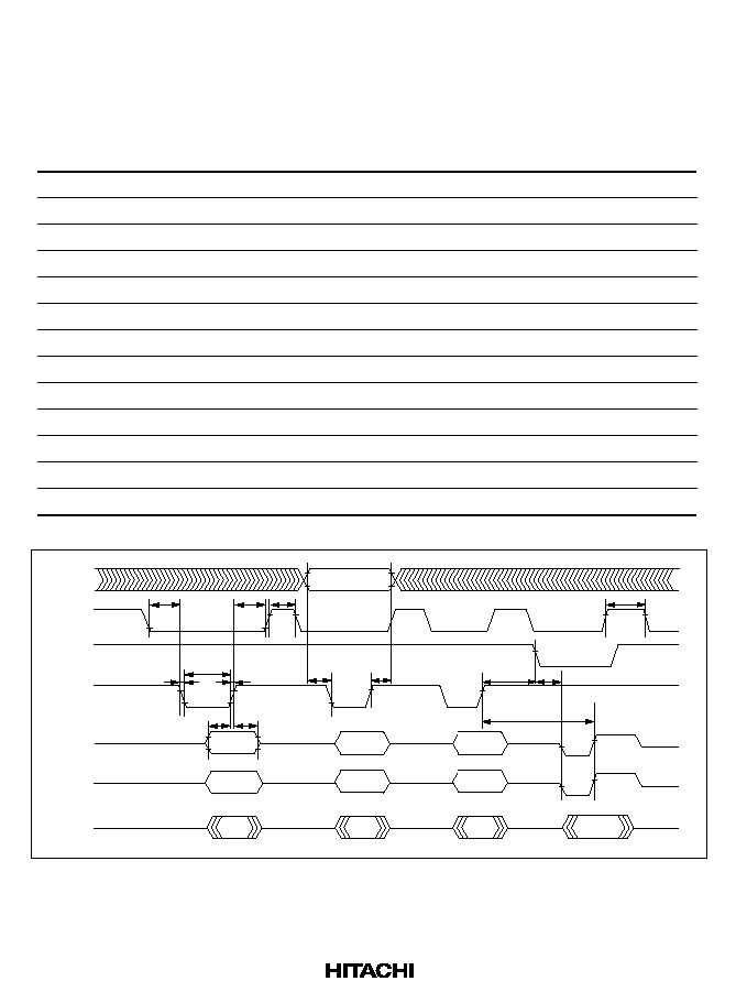
530
Auto-Program Mode
∑
AC Characteristics
Table 21.16
AC Characteristics in Auto-Program Mode
(Conditions: V
CC
= 5.0 V ±10%, V
SS
= 0 V, T
a
= 25∞C ±5∞C)
Item
Symbol
Min
Max
Unit
Notes
Command write cycle
t
nxtc
20
µ
s
CE
hold time
t
ceh
0
ns
CE
setup time
t
ces
0
ns
Data hold time
t
dh
50
ns
Data setup time
t
ds
50
ns
Programming pulse width
t
wep
70
ns
Status polling start time
t
wsts
1
ms
Status polling access time
t
spa
150
ns
Address setup time
t
as
0
ns
Address hold time
t
ah
60
ns
Memory write time
t
write
1
3000
ms
WE
rise time
t
r
30
ns
WE
fall time
t
f
30
ns
Address stable
CE
Address
Data
FO6
FO7
OE
WE
t
as
t
ah
t
dh
t
ds
t
f
t
r
t
wep
t
wsts
t
write
t
spa
t
nxtc
t
nxtc
t
ceh
t
ces
Programming operation
end identification signal
Data transfer
1 byte ... 128 bytes
Programming normal
end identification signal
Programming wait
H'40
Data
Data
FO0 to FO5 = 0
Figure 21.20 Auto-Program Mode Timing Waveforms

531
∑
Notes on Use of Auto-Program Mode
1. In auto-program mode, 128 bytes are programmed simultaneously. This should be carried out
by executing 128 consecutive byte transfers.
2. A 128-byte data transfer is necessary even when programming fewer than 128 bytes. In this
case, H'FF data must be written to the extra addresses.
3. The lower 8 bits of the transfer address must be H'00 or H'80. If a value other than a valid
address is input, processing will switch to a memory write operation but a write error will be
flagged.
4. Memory address transfer is performed in the second cycle (figure 21.19). Do not perform
transfer after the second cycle.
5. Do not perform a command write during a programming operation.
6. Perform one auto-programming operation for a 128-byte block for each address.
Characteristics are not guaranteed for two or more programming operations.
7. Confirm normal end of auto-programming by checking FO6. Alternatively, status read mode
can also be used for this purpose (in FO7 status polling, the pin is the auto-program operation
end identification pin).
8. Status polling FO6 and FO7 pin information is retained until the next command write. As long
as the next command write has not been performed, reading is possible by enabling
CE and
OE.

532
Auto-Erase Mode
∑
AC Characteristics
Table 21.17
AC Characteristics in Auto-Erase Mode
(Conditions: V
CC
= 5.0 V ±10%, V
SS
= 0 V, T
a
= 25∞C ±5∞C)
Item
Symbol
Min
Max
Unit
Notes
Command write cycle
t
nxtc
20
µ
s
CE
hold time
t
ceh
0
ns
CE
setup time
t
ces
0
ns
Data hold time
t
dh
50
ns
Data setup time
t
ds
50
ns
Programming pulse width
t
wep
70
ns
Status polling start time
t
ests
1
ms
Status polling access time
t
spa
150
ns
Memory erase time
t
erase
100
40000
ms
WE
rise time
t
r
30
ns
WE
fall time
t
f
30
ns
CE
Address
Data
FO6
FO7
OE
WE
t
ests
t
erase
t
spa
t
dh
t
ds
t
f
t
r
t
wep
t
nxtc
t
nxtc
t
ceh
t
ces
Erase end
identification signal
Erase normal end
confirmation signal
H'20
H'20
FO0 to FO5 = 0
(100 to 40000 ms)
DL
in
CL
in
Figure 21.21 Auto-Erase Mode Timing Waveforms

533
∑
Notes on Use of Erase-Program Mode
1. Auto-erase mode supports only total memory erasing.
2. Do not perform a command write during auto-erasing.
3. Confirm normal end of auto-erasing by checking FO6. Alternatively, status read mode can also
be used for this purpose (in FO7 status polling, the pin is the auto-erase operation end
identification pin).
4. Status polling FO6 and FO7 pin information is retained until the next command write. As long
as the next command write has not been performed, reading is possible by enabling
CE and
OE.
Status Read Mode
1. Status read mode is used to identify what kind of abnormal end has occurred. This mode
should be used if an abnormal end occurs in auto-program or auto-erase mode.
2. The return code is retained until a command write for a mode other than status read mode is
executed.
Table 21.18
AC Characteristics in Status Read Mode
(Conditions: V
CC
= 5.0 V ±10%, V
SS
= 0 V, T
a
= 25∞C ±5∞C)
Item
Symbol
Min
Max
Unit
Notes
Command write cycle
t
nxtc
20
µ
s
CE
hold time
t
ceh
0
ns
CE
setup time
t
ces
0
ns
Data hold time
t
dh
50
ns
Data setup time
t
ds
50
ns
Programming pulse width
t
wep
70
ns
OE
output delay time
t
oe
150
ns
Disable delay time
t
df
100
ns
CE
output delay time
t
ce
150
ns
WE
rise time
t
r
30
ns
WE
fall time
t
f
30
ns

534
CE
Address
Data
OE
WE
t
df
t
f
t
r
t
wep
t
f
t
r
t
wep
t
nxtc
t
nxtc
t
ds
t
dh
t
ds
t
dh
t
nxtc
t
ceh
t
ceh
t
oe
t
ces
t
ces
t
ce
H'71
H'71
Note: FO2 and FO3 are undefined.
Figure 21.22 Status Read Mode Timing Waveforms
Table 21.19
Status Read Mode Return Codes
Pin
FO7
FO6
FO5
FO4
FO3
FO2
FO1
FO0
Attribute
Normal end
identification
Command
error
Programming
error
Erase
error
--
--
Programming
or erase
count
exceeded
Valid
address
error
Initial value
0
0
0
0
0
0
0
0
Indications
Normal end:
0
Abnormal
end: 1
Command
error: 1
Otherwise:
0
Programming
error: 1
Otherwise: 0
Erase
error: 1
Otherwise:
0
--
--
Count
exceeded: 1
Otherwise: 0
Valid
address
error: 1
Otherwise:
0
Note: FO2 and FO3 are undefined.
Status Polling
1. In FO7 status polling, FO7 is a flag that indicates the operating status in auto-program or auto-
erase mode.
2. In FO6 status polling, FO6 is a flag that indicates a normal or abnormal end in auto-program or
auto-erase mode.
Table 21.20
Status Polling Output Truth Table
Pin
Internal Operation
in Progress
Abnormal End
--
Normal End
FO7
0
1
0
1
FO6
0
0
1
1
FO0≠FO5
0
0
0
0
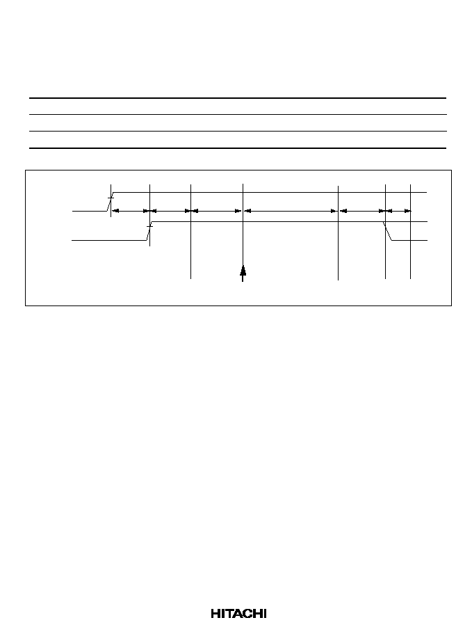
535
Writer Mode Transition Time: Commands cannot be accepted during the oscillation settling
period or the writer mode setup period. After the writer mode setup time, a transition is made to
memory read mode.
Table 21.21
Stipulated Transition Times to Command Wait State
Item
Symbol
Min
Max
Unit
Notes
Standby release (oscillation settling time)
t
osc1
10
ms
Writer mode setup time
t
bmv
10
ms
V
CC
hold time
t
dwn
0
ms
V
CC
RES
Memory
read mode
Command
wait state
Command
wait state
Normal/
abnormal
end
identification
Command acceptance
Auto-program mode
Auto-erase mode
t
osc1
t
bmv
t
dwn
Figure 21.23 Oscillation Settling Time, Boot Program Transfer Time,
and Power-Down Sequence
Cautions on Memory Programming
1. When programming addresses which have previously been programmed, carry out auto-
erasing before auto-programming.
2. When performing programming using writer mode on a chip that has been programmed/erased
in an on-board programming mode, auto-erasing is recommended before carrying out auto-
programming.
Notes: 1. The flash memory is initially in the erased state when the device is shipped by Hitachi.
For other chips for which the erasure history is unknown, it is recommended that auto-
erasing be executed to check and supplement the initialization (erase) level.
2. Auto-programming should be performed once only on the same address block.

536
21.6
Flash Memory Programming and Erasing Precautions
Read these precautions before using writer mode, on-board programming mode, or flash memory
emulation by RAM.
(1) Program with the specified voltage and timing.
When using a PROM programmer to reprogram the on-chip flash memory in the single-power-
supply model (S-mask model), use a PROM programmer that supports the Hitachi microcomputer
device type with 64-kbyte on-chip flash memory (5.0 V programming voltage), do not set the
programmer to the HN28F101 3.3 V programming voltage and only use the specified socket
adapter. Failure to observe these precautions may result in damage to the device.
(2) Before programming, check that the chip is correctly mounted in the PROM
programmer.
Overcurrent damage to the device can occur if the index marks on the PROM programmer socket,
socket adapter, and chip are not correctly aligned.
(3) Don't touch the socket adapter or chip while programming.
Touching either of these can cause contact faults and write errors.
(4) Set H'FF as the PROM programmer buffer data for addresses H'F780 to H'1FFFF.
The H8/3337SF PROM size is 60 kbytes. Addresses H'F780 to H'1FFFF always read H'FF, so if
H'FF is not specified as programmer data, a block error will occur.
(5) Use the recommended algorithms for programming and erasing flash memory.
These algorithms are designed to program and erase without subjecting the device to voltage stress
and without sacrificing the reliability of programmed data.
Before setting the program (P) or erase (E) bit in flash memory control register 1 (FLMCR1), set
the watchdog timer to ensure that the P or E bit does not remain set for more than the specified
time.
(6) For details on interrupt handling while flash memory is being programmed or erased,
see section 21.4.6, Interrupt Handling during Flash Memory Programming and Erasing.
(7) Cautions on Accessing Flash Memory Control Registers
1. Flash memory control register access state in each operating mode
The H8/3337SF has flash memory control registers located at addresses H'FF80 (FLMCR1),
H'FF81 (FLMCR2), and H'FF83 (EBR2). These registers can only be accessed when the
FLSHE bit is set to 1 in the wait-state control register (WSCR).
Table 21.22 shows the area accessed for the above addresses in each mode, when FLSHE = 0
and when FLSHE = 1.

537
Table 21.22
Area Accessed in Each Mode with FLSHE = 0 and FLSHE = 1
Mode 1
Mode 2
Mode 3
FLSHE = 1
Reserved area
(always H'FF)
Flash memory control register initial values
FLLMCR1 = H'80
FLMCR2 = H'00
EBR2 = H'00
FLSHE = 0
External address space
External address space
Reserved area
(always H'FF)
2. When a flash memory control register is accessed in mode 2 (expanded mode with on-chip
ROM enabled)
When a flash memory control register is accessed in mode 2, it can be read or written to if
FLSHE = 1, but if FLSHE = 0, external address space will be accessed. It is therefore essential
to confirm that FLSHE is set to 1 before accessing these registers.
3. To check whether FLSHE = 0 or 1 in mode 3 (single-chip mode)
When address H'FF80 is accessed in mode 3, if FLSHE = 1, FLMCR1 is read/written to, and
its initial value after a reset is H'80. When FLSHE = 0, however, this address is a reserved area
that cannot be modified and always reads H'FF.

538

539
Section 22 Power-Down State
22.1
Overview
The H8/3337 Series and H8/3397 Series have a power-down state that greatly reduces power
consumption by stopping some or all of the chip functions. The power-down state includes three
modes:
1. Sleep mode
2. Software standby mode
3. Hardware standby mode
Table 22.1 lists the conditions for entering and leaving the power-down modes. It also indicates
the status of the CPU, on-chip supporting modules, etc. in each power-down mode.
Table 22.1
Power-Down State
State
Mode
Entering
Procedure
Clock
CPU
CPU
Reg's.
Sup.
Mod.
RAM
I/O
Ports
Exiting
Methods
Sleep
mode
Execute
SLEEP
instruction
Active
Halted
Held
Active
Held
Held
∑
Interrupt
∑
RES
∑
STBY
Software
standby
mode
Set SSBY bit
in SYSCR to
1, then
execute
SLEEP
instruction
Halted
Halted
Held
Halted
and
initialized
Held
Held
∑
NMI
∑
IRQ
0
≠
IRQ
2
IRQ
6
(incl.
KEYIN
0
≠
KEYIN
7
)
∑
RES
∑
STBY
Hardware
standby
mode
Set
STBY
pin to low
level
Halted
Halted
Undeter-
mined
Halted
and
initialized
Held
High
impe-
dance
state
∑
STBY
and
RES
Note:
SYSCR: System control register
SSBY:
Software standby bit

540
22.1.1
System Control Register (SYSCR)
Four of the eight bits in the system control register (SYSCR) control the power-down state. These
are bit 7 (SSBY) and bits 6 to 4 (STS2 to STS0). See table 22.2.
Table 22.2
System Control Register
Name
Abbreviation
R/W
Initial Value
Address
System control register
SYSCR
R/W
H'09
H'FFC4
B
it
7
6
5
4
3
2
1
0
SSBY
STS2
STS1
STS0
XRST
NMIEG
HIE
RAME
Initial value
0
0
0
0
1
0
0
1
Read/Write
R/W
R/W
R/W
R/W
R
R/W
R/W
R/W
Bit 7--Software Standby (SSBY): This bit enables or disables the transition to software standby
mode.
On recovery from the software standby mode by an external interrupt, SSBY remains set to 1. To
clear this bit, software must write a 0.
Bit 7: SSBY
Description
0
The SLEEP instruction causes a transition to sleep mode.
(Initial value)
1
The SLEEP instruction causes a transition to software standby mode.

541
Bits 6 to 4--Standby Timer Select 2 to 0 (STS2 to STS0): These bits select the clock settling
time when the chip recovers from software standby mode by an external interrupt. During the
selected time, the clock oscillator runs but the CPU and on-chip supporting modules remain in
standby. Set bits STS2 to STS0 according to the clock frequency to obtain a settling time of at
least 8 ms. See table 22.3.
∑
ZTAT and Mask ROM Versions
Bit 6: STS2
Bit 5: STS1
Bit 4: STS0
Description
0
0
0
Settling time = 8,192 states
(Initial value)
1
Settling time = 16,384 states
1
0
Settling time = 32,768 states
1
Settling time = 65,536 states
1
0
--
Settling time = 131,072 states
1
--
Unused
∑
F-ZTAT Version
Bit 6: STS2
Bit 5: STS1
Bit 4: STS0
Description
0
0
0
Settling time = 8,192 states
(Initial value)
1
Settling time = 16,384 states
1
0
Settling time = 32,768 states
1
Settling time = 65,536 states
1
0
0
Settling time = 131,072 states
1
Settling time = 1,024 states
1
--
Unused
Notes: When 1,024 states (STS2 to STS0 = 101) is selected, the following points should be noted.
If a period exceeding ¯p/1,024 (e.g. ¯p/2,048) is specified when selecting the 8-bit timer,
PWM timer, or watchdog timer clock, the counter in the timer will not count up normally
when 1,024 states is specified for the setting time. To avoid this problem, set the STS value
just before the transition to software standby mode (before executing the SLEEP
instruction), and re-set the value of STS2 to STS0 to a value from 000 to 100 directly after
software standby mode is cleared by an interrupt.

542
22.2
Sleep Mode
22.2.1
Transition to Sleep Mode
When the SSBY bit in the system control register is cleared to 0, execution of the SLEEP
instruction causes a transition from the program execution state to sleep mode. After executing the
SLEEP instruction, the CPU halts, but the contents of its internal registers remain unchanged. The
on-chip supporting modules continue to operate normally.
22.2.2
Exit from Sleep Mode
The chip exits sleep mode when it receives an internal or external interrupt request, or a low input
at the
RES or STBY pin.
Exit by Interrupt: An interrupt releases sleep mode and starts the CPU's interrupt-handling
sequence.
If an interrupt from an on-chip supporting module is disabled by the corresponding enable/disable
bit in the module's control register, the interrupt cannot be requested, so it cannot wake the chip
up. Similarly, the CPU cannot be awakened by an interrupt other than NMI if the I (interrupt
mask) bit is set when the SLEEP instruction is executed.
Exit by
RES pin: When the RES pin goes low, the chip exits from sleep mode to the reset state.
Exit by
STBY pin: When the STBY pin goes low, the chip exits from sleep mode to hardware
standby mode.

543
22.3
Software Standby Mode
22.3.1
Transition to Software Standby Mode
To enter software standby mode, set the standby bit (SSBY) in the system control register
(SYSCR) to 1, then execute the SLEEP instruction.
In software standby mode, the system clock stops and chip functions halt, including both CPU
functions and the functions of the on-chip supporting modules. Power consumption is reduced to
an extremely low level. The on-chip supporting modules and their registers are reset to their initial
states, but as long as a minimum necessary voltage supply is maintained, the contents of the CPU
registers and on-chip RAM remain unchanged. I/O ports retain their states.
22.3.2
Exit from Software Standby Mode
The chip can be brought out of software standby mode by an
RES input, STBY input, or external
interrupt input at the
NMI pin, IRQ
0
to
IRQ
2
pins, or
IRQ
6
pin (including
KEYIN
0
to
KEYIN
7
).
Exit by Interrupt: When an NMI, IRQ
0
, IRQ
1
, IRQ
2
, or IRQ
6
interrupt request signal is input, the
clock oscillator begins operating. After the waiting time set in bits STS2 to STS0 of SYSCR, a
stable clock is supplied to the entire chip, software standby mode is released, and interrupt
exception-handling begins. IRQ
3
, IRQ
4
, IRQ
5
, and IRQ
7
interrupts should be disabled before the
transition to software standby (clear IRQ3E, IRQ4E, IRQ5E, and IRQ7E to 0).
Exit by
RES Pin: When the RES input goes low, the clock oscillator begins operating. When
RES is brought to the high level (after allowing time for the clock oscillator to settle), the CPU
starts reset exception handling. Be sure to hold
RES low long enough for clock oscillation to
stabilize.
Exit by
STBY Pin: When the STBY input goes low, the chip exits from software standby mode
to hardware standby mode.

544
22.3.3
Clock Settling Time for Exit from Software Standby Mode
Set bits STS2 to STS0 in SYSCR as follows:
∑
Crystal oscillator
Set STS2 to STS0 for a settling time of at least 8 ms. Table 22.3 lists the settling times selected
by these bits at several clock frequencies.
∑
External clock
The STS bits can be set to any value. The shortest time setting (STS2=STS1=STS0=0) is
recommended in most cases. When 1,024 states (STS2 to STS0 = 101) is selected, the
following points should be noted.
If a period exceeding ¯p/1,024 (e.g. ¯p/2,048) is specified when selecting the 8-bit timer,
PWM timer, or watchdog timer clock, the counter in the timer will not count up normally when
1,024 states is specified for the setting time. To avoid this problem, set the STS value just
before the transition to software standby mode (before executing the SLEEP instruction), and
re-set the value of STS2 to STS0 to a value from 000 to 100 directly after software standby
mode is cleared by an interrupt.
Table 22.3
Times Set by Standby Timer Select Bits (Unit: ms)
Settling
Time
System Clock Frequency (MHz)
STS2
STS1
STS0
(States)
16
12
10
8
6
4
2
1
0.5
0
0
0
8,192
0.51
0.65
0.8
1.0
1.3
2.0
4.1
8.2
16.4
0
0
1
16,384
1.0
1.3
1.6
2.0
2.7
4.1
8.2
16.4
32.8
0
1
0
32,768
2.0
2.7
3.3
4.1
5.5
8.2
16.4
32.8
65.5
0
1
1
65,536
4.1
5.5
6.6
8.2
10.9
16.4
32.8
65.5
131.1
1
0
0/--
*
131,072
8.2
10.9
13.1
16.4
21.8
32.8
65.5
131.1 262.1
Note:
Recommended values are printed in boldface.
*
F-ZTAT version/ZTAT and mask-ROM versions.
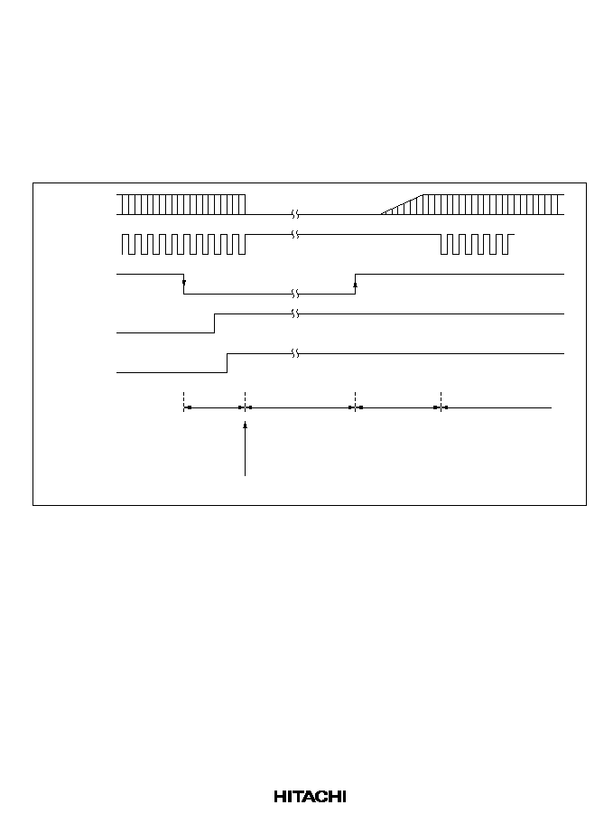
545
22.3.4
Sample Application of Software Standby Mode
In this example the chip enters the software standby mode when
NMI
goes low and exits when
NMI
goes high, as shown in figure 22.1.
The NMI edge bit (NMIEG) in the system control register is originally cleared to 0, selecting the
falling edge. When
NMI
goes low, the
NMI
interrupt handling routine sets NMIEG to 1, sets
SSBY to 1 (selecting the rising edge), then executes the SLEEP instruction. The chip enters
software standby mode. It recovers from software standby mode on the next rising edge of
NMI
.
¯
NMI
NMIEG
SSBY
NMI interrupt
handler
NMIEG = 1
SSBY = 1
Software standby
mode (power-
down state)
Settling time
SLEEP instruction
NMI interrupt
handler
Clock
oscillator
Figure 22.1 NMI Timing in Software Standby Mode (Application Example)
546
22.3.5
Application Notes
1. The I/O ports retain their present states in software standby mode. Thus, current dissipation
caused by the output current is not reduced.
; Set the SSBY bit
; Execute the SLEEP instruction
BSET
SLEEP
∑
∑
∑
∑
∑
∑
∑
∑
∑
∑
∑
∑
#7, @SYSCR:8
; Set the SSBY bit
; Write the "SLEEP" code (H'0180)
; to RAM
; Write the "RTS" code (H'5470)
; to RAM
; Subroutine branch to that location
*
Registers and RAM addresses are arbitrary.
BSET
MOV. W
MOV. W
MOV. W
MOV. W
JSR
#7, @SYSCR:8
#H' 0180, R0
R0, @H'FF00
#H' 5470, R0
R0, @H'FF02
@H'FF00
Replace the underlined part
(SLEEP instruction) with
the code shown below.
Note:
When a SLEEP instruction is executed in ROM, the current responsible for this bug also
flows when a sleep mode transition is made. Therefore, to further reduce current
dissipation in sleep mode, also, software should be modified so that the SLEEP instruction
is executed in RAM when making a sleep mode transition.

547
22.4
Hardware Standby Mode
22.4.1
Transition to Hardware Standby Mode
Regardless of its current state, the chip enters hardware standby mode whenever the
STBY
pin
goes low.
Hardware standby mode reduces power consumption drastically by halting the CPU, stopping all
the functions of the on-chip supporting modules, and placing I/O ports in the high-impedance
state. The registers of the on-chip supporting modules are reset to their initial values. Only the on-
chip RAM is held unchanged, provided the minimum necessary voltage supply is maintained.
Notes: 1. The RAME bit in the system control register should be cleared to 0 before the
STBY
pin goes low.
2. Do not change the inputs at the mode pins (MD
1
, MD
0
) during hardware standby mode.
Be particularly careful not to let both mode pins go low in hardware standby mode,
since that places the chip in writer mode and increases current dissipation.
22.4.2
Recovery from Hardware Standby Mode
Recovery from the hardware standby mode requires inputs at both the
STBY and RES pins. When
the
STBY
pin goes high, the clock oscillator begins running. The
RES pin should be low at this
time and should be held low long enough for the clock to stabilize. When the
RES pin changes
from low to high, the reset sequence is executed and the chip returns to the program execution
state.
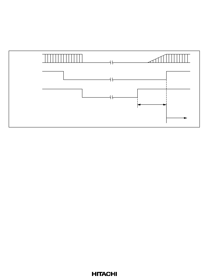
548
22.4.3
Timing Relationships in Hardware Standby Mode
Figure 22.2 shows the timing relationships in hardware standby mode.
In the sequence shown, first
RES goes low, then STBY goes low, at which point the chip enters
hardware standby mode. To recover, first
STBY goes high, then after the clock settling time, RES
goes high.
RES
STBY
Clock pulse
generator
Clock settling
time
Restart
Figure 22.2 Hardware Standby Mode Timing

549
Section 23 Electrical Characteristics
23.1
Absolute Maximum Ratings
Table 23.1 lists the absolute maximum ratings.
Table 23.1
Absolute Maximum Ratings
Item
Symbol
Rating
Unit
Supply voltage
V
CC
≠0.3 to +7.0
V
Flash memory programming
voltage (Dual-power-supply
F-ZTATTM version)
FV
PP
≠0.3 to +13.0
V
Programming voltage
V
PP
≠0.3 to +13.5
V
Input voltage
Pins other than
ports 7, MD
1
,
V
in
≠0.3 to V
CC
+ 0.3
V
Port 7
V
in
≠0.3 to AV
CC
+ 0.3
V
MD
1
V
in
Dual-power-supply F-ZTAT version:
≠0.3 to +13.0
Other versions: ≠0.3 to V
CC
+ 0.3
V
Analog supply voltage
AV
CC
≠0.3 to +7.0
V
Analog input voltage
V
AN
≠0.3 to AV
CC
+ 0.3
V
Operating temperature
T
opr
Regular specifications: ≠20 to +75
∞C
Wide-range specifications: ≠40 to +85
∞C
Storage temperature
T
stg
≠55 to +125
∞C
Note:
Exceeding the absolute maximum ratings shown in table 23.1 can permanently destroy
the chip.
*
*
FV
PP
must not exceed 13 V and V
PP
must not exceed 13.5 V, including peak overshoot. In
the dual-power-supply F-ZTAT version, MD
1
must not exceed 13 V, including peak
overshoot.

550
23.2
Electrical Characteristics
23.2.1
DC Characteristics
Table 23.2 lists the DC characteristics of the 5-V version. Table 23.3 lists the DC characteristics of
4-V version. Table 23.4 lists the DC characteristics of the 3-V version. Table 23.5 gives the
allowable current output values of the 5-V and 4-V versions. Table 23.6 gives the allowable
current output values of the 3-V version. Bus drive characteristics common to 5 V, 4 V and 3 V
versions are listed in table 23.7.
Table 23.2
DC Characteristics (5-V Version)
Conditions: V
CC
= 5.0 V ±10%, AV
CC
= 5.0 V ±10%
*1
, V
SS
= AV
SS
= 0 V, Ta = ≠20∞C to +75∞C
(regular specifications), Ta = ≠40∞C to +85∞C (wide-range specifications)
Item
Symbol
Min
Typ
Max
Unit
Test
Conditions
Schmitt
P6
7
to P6
0
*
4
,
(1)
V
T
≠
1.0
--
--
V
trigger input
IRQ
2
to
IRQ
0
*
5
,
V
T
+
--
--
V
CC
◊
0.7
voltage
IRQ
7
to
IRQ
3
V
T
+
≠ V
T
≠
0.4
--
--
Input high
voltage
RES
,
STBY
,
MD
1
, MD
0
,
EXTAL,
NMI
(2)
V
IH
V
CC
≠ 0.7
--
V
CC
+ 0.3
V
SCL, SDA
V
CC
◊
0.7
--
V
CC
+ 0.3
P7
7
to P7
0
2.0
--
AV
CC
+ 0.3
All input pins other
than (1) and (2)
above
2.0
--
V
CC
+ 0.3
Input low
voltage
RES
,
STBY
,
MD
1
, MD
0
(3)
V
IL
≠0.3
--
0.5
V
SCL, SDA
≠0.3
--
1.0
All input pins other
than (1) and (3)
above
≠0.3
--
0.8
Output high
All output pins
*
6
V
OH
V
CC
≠ 0.5
--
--
V
I
OH
= ≠200 µA
voltage
3.5
--
--
I
OH
= ≠1.0mA

551
Item
Symbol
Min
Typ
Max
Unit
Test
Conditions
Output low
All output pins
*
6
V
OL
--
--
0.4
V
I
OL
= 1.6 mA
voltage
P1
7
to P1
0
,
P2
7
to P2
0
--
--
1.0
I
OL
= 10.0 mA
Input
RES
,
STBY
| I
in
|
--
--
10.0
µA
Vin = 0.5 V to
leakage
NMI
, MD
1
, MD
0
--
--
1.0
V
CC
≠ 0.5 V
current
P7
7
to P7
0
--
--
1.0
Vin = 0.5 V to
AV
CC
≠ 0.5 V
Leakage
current in
three-state
(off state)
Ports 1 to 6, 8, 9
| I
TSI
|
--
--
1.0
µA
Vin = 0.5 V to
V
CC
≠ 0.5 V
Input pull-up Ports 1 to 3
≠I
P
30
--
250
µA
Vin = 0 V
MOS
current
Ports 6
60
--
500
Input
capacitance
STBY
(dual-power-
supply F-ZTAT
version)
(4)
C
in
--
--
120
pF
Vin = 0 V,
F = 1 MHz,
Ta = 25∞C
RES
,
STBY
(except dual-
power-supply
F-ZTAT
version)
--
--
60
NMI
, MD
1
--
--
50
f = 1 MHz,
P9
7
, P8
6
--
--
20
Ta = 25∞C
All input pins other
than (4)
--
--
15
Current
Normal operation
I
CC
--
27
45
mA
f = 12 MHz
dissipation
*
2
--
36
60
f = 16 MHz
Sleep mode
--
18
30
f = 12 MHz
--
24
40
f = 16 MHz
Standby modes
*
3
--
0.01
5.0
µA
Ta
50∞C
--
--
20.0
50∞C < Ta

552
Item
Symbol
Min
Typ
Max
Unit
Test
Conditions
Analog
supply
During A/D
conversion
AI
CC
--
2.0
5.0
mA
current
During A/D and D/A
conversion
--
2.0
5.0
A/D and D/A
conversion idle
--
0.01
5.0
µA
AV
CC
= 2.0 V
to 5.5 V
Analog supply voltage
*
1
AV
CC
4.5
--
5.5
V
During
operation
2.0
--
5.5
While idle or
when not in
use
RAM standby voltage
V
RAM
2.0
--
--
V
Notes:
*
1 Even when the A/D and D/A converters are not used, connect AV
CC
to power supply V
CC
and keep the applied voltage between 2.0 V and 5.5 V.
*
2 Current dissipation values assume that V
IH
min
= V
CC
≠ 0.5 V, V
IL max
= 0.5 V, all output
pins are in the no-load state, and all input pull-up transistors are off.
*
3 For these values it is assumed that V
RAM
V
CC
< 4.5 V and V
IH
min
= V
CC
◊
0.9,
V
IL max
= 0.3 V.
*
4 P6
7
to P6
0
include supporting module inputs multiplexed with them.
*
5
IRQ
2
includes
ADTRG
multiplexed with it.
*
6 Applies when IICE = 0. The output low level is determined separately when the bus
drive function is selected.

553
Table 23.3
DC Characteristics (4-V Version)
Conditions: V
CC
= 4.0 V to 5.5 V, AV
CC
= 4.0 V to 5.5 V
*1
, V
SS
= AV
SS
= 0 V, Ta = ≠20∞C to
+75∞C (regular specifications), Ta = ≠40∞C to +85∞C (wide-range specifications)
Item
Symbol
Min
Typ
Max
Unit
Test
Conditions
Schmitt
P6
7
to P6
0
*
4
,
(1)
V
T
≠
1.0
--
--
V
V
CC
= 4.5 V to
trigger input
IRQ
2
to
IRQ
0
*
5
,
V
T
+
--
--
V
CC
◊
0.7
5.5 V
voltage
IRQ
7
to
IRQ
3
V
T
+
≠ V
T
≠
0.4
--
--
V
T
≠
0.8
--
--
V
CC
= 4.0 V to
V
T
+
--
--
V
CC
◊
0.7
4.5 V
V
T
+
≠ V
T
≠
0.3
--
--
Input high
voltage
RES
,
STBY
,
MD
1
, MD
0
,
EXTAL,
NMI
(2)
V
IH
V
CC
≠ 0.7
--
V
CC
+ 0.3
V
SCL, SDA
V
CC
◊
0.7
--
V
CC
+ 0.3
P7
7
to P7
0
2.0
--
AV
CC
+ 0.3
All input pins other
than (1) and (2)
above
2.0
--
V
CC
+ 0.3
Input low
voltage
RES
,
STBY
,
MD
1
, MD
0
(3)
V
IL
≠0.3
--
0.5
V
SCL, SDA
≠0.3
--
1.0
V
CC
= 4.5 V to
5.5 V
≠0.3
--
0.8
V
CC
= 4.0 V to
4.5 V
All input pins other
than (1) and (3)
≠0.3
--
0.8
V
CC
= 4.5 V to
5.5 V
above
≠0.3
--
0.6
V
CC
= 4.0 V to
4.5 V
Output high
All output pins
*
6
V
OH
V
CC
≠ 0.5
--
--
V
I
OH
= ≠200 µA
voltage
3.5
--
--
I
OH
= ≠1.0 mA,
V
CC
= 4.5 V to
5.5 V
2.8
--
--
I
OH
= ≠1.0 mA,
V
CC
= 4.0 V to
4.5 V

554
Item
Symbol
Min
Typ
Max
Unit
Test
Conditions
Output low
All output pins
*
6
V
OL
--
--
0.4
V
I
OL
= 1.6 mA
voltage
P1
7
to P1
0
,
P2
7
to P2
0
--
--
1.0
I
OL
= 10.0 mA
Input
RES
,
STBY
| I
in
|
--
--
10.0
µA
Vin = 0.5 V to
leakage
NMI
, MD
1
, MD
0
--
--
1.0
V
CC
≠ 0.5 V
current
P7
7
to P7
0
--
--
1.0
Vin = 0.5 V to
AV
CC
≠ 0.5 V
Leakage
current in
three-state
(off state)
Ports 1 to 6, 8, 9
| I
TSI
|
--
--
1.0
µA
Vin = 0.5 V to
V
CC
≠ 0.5 V
Input pull-up Ports 1 to 3
≠I
P
30
--
250
µA
Vin = 0 V,
MOS
current
Ports 6
60
--
500
V
CC
= 4.5 V to
5.5 V
Ports 1 to 3
20
--
200
Vin = 0 V,
Ports 6
40
--
400
V
CC
= 4.0 V to
4.5 V
Input
capacitance
STBY
(dual-power-
supply F-ZTAT
version)
(4)
C
in
--
--
120
pF
Vin = 0 V,
F = 1 MHz,
Ta = 25∞C
RES
,
STBY
(except dual-
power-supply
F-ZTAT
version)
--
--
60
NMI
, MD
1
--
--
50
f = 1 MHz,
P9
7
, P8
6
--
--
20
Ta = 25∞C
All input pins other
than (4) above
--
--
15

555
Item
Symbol
Min
Typ
Max
Unit
Test
Conditions
Current
Normal operation
I
CC
--
27
45
mA
f = 12 MHz
dissipation
*
2
--
36
60
f = 16 MHz,
V
CC
= 4.5 V to
5.5 V
Sleep mode
--
18
30
f = 12 MHz
--
24
40
f = 16 MHz,
V
CC
= 4.5 V to
5.5 V
Standby modes
*
3
--
0.01
5.0
µA
Ta
50∞C
--
--
20.0
50∞C < Ta
Analog
supply
During A/D
conversion
AI
CC
--
2.0
5.0
mA
current
During A/D and D/A
conversion
--
2.0
5.0
A/D and D/A
conversion idle
--
0.01
5.0
µA
AV
CC
= 2.0 V
to 5.5 V
Analog supply voltage
*
1
AV
CC
4.0
--
5.5
V
During
operation
2.0
--
5.5
While idle or
when not in
use
RAM standby voltage
V
RAM
2.0
--
--
V
Notes:
*
1 Even when the A/D and D/A converters are not used, connect AV
CC
to power supply V
CC
and keep the applied voltage between 2.0 V and 5.5 V.
*
2 Current dissipation values assume that V
IH min
= V
CC
≠ 0.5 V, V
IL max
= 0.5 V, all output
pins are in the no-load state, and all input pull-up transistors are off.
*
3 For these values it is assumed that V
RAM
V
CC
< 4.0 V and V
IH min
= V
CC
◊
0.9, V
IL max
=
0.3 V.
*
4 P6
7
to P6
0
include supporting module inputs multiplexed with them.
*
5
IRQ
2
includes
ADTRG
multiplexed with it.
*
6 Applies when IICE = 0. The output low level is determined separately when the bus
drive function is selected.

556
Table 23.4
DC Characteristics (3-V Version)
Conditions: V
CC
= 2.7 V to 5.5 V
*7
, AV
CC
= 2.7 V to 5.5 V
*1, *7
, V
SS
= AV
SS
= 0 V, Ta = ≠20∞C to
+75∞C
Item
Symbol
Min
Typ
Max
Unit
Test
Conditions
Schmitt
P6
7
to P6
0
*
4
,
(1)
V
T
≠
V
CC
◊
0.15 --
--
V
trigger input
IRQ
2
to
IRQ
0
*
5
,
V
T
+
--
--
V
CC
◊
0.7
voltage
IRQ
7
to IRQ
3
V
T
+
≠ V
T
≠
0.2
--
--
Input high
voltage
RES
,
STBY
,
MD
1
, MD
0
,
EXTAL,
NMI
(2)
V
IH
V
CC
◊
0.9
--
V
CC
+ 0.3
V
SCL, SDA
V
CC
◊
0.7
--
V
CC
+ 0.3
P7
7
to P7
0
AV
CC
◊
0.7 --
AV
CC
+ 0.3
All input pins other
than (1) and (2)
above
V
CC
◊
0.7
--
V
CC
+ 0.3
Input low
voltage
*
4
RES
,
STBY
,
MD
1
, MD
0
(3)
V
IL
≠0.3
--
V
CC
◊
0.1
V
SCL, SDA
≠0.3
--
V
CC
◊
0.15
All input pins other
than (1) and (3)
above
≠0.3
--
V
CC
◊
0.15
Output high
All output pins
*
6
V
OH
V
CC
≠ 0.5
--
--
V
I
OH
= ≠200 µA
voltage
V
CC
≠ 1.0
--
--
I
OH
= ≠1 mA
Output low
All output pins
*
6
V
OL
--
--
0.4
V
I
OL
= 0.8 mA
voltage
P1
7
to P1
0
,
P2
7
to P2
0
--
--
0.4
I
OL
= 1.6 mA
Input
RES
,
STBY
| I
in
|
--
--
10.0
µA
Vin = 0.5 V to
leakage
NMI
, MD
1
, MD
0
--
--
1.0
V
CC
≠ 0.5 V
current
P7
7
to P7
0
--
--
1.0
Vin = 0.5 V to
AV
CC
≠ 0.5 V
Leakage
current in
three-state
(off state)
Ports 1 to 6, 8, 9
| I
TSI
|
--
--
1.0
µA
Vin = 0.5 V to
V
CC
≠ 0.5 V

557
Item
Symbol
Min
Typ
Max
Unit
Test
Conditions
Input pull-up Ports 1 to 3
≠I
P
3
--
120
µA
Vin = 0 V,
MOS
current
Ports 6
30
--
250
V
CC
= 2.7 V to
3.6 V
Input
capacitance
STBY
(dual-power-
supply F-ZTAT
version)
(4)
C
in
--
--
120
pF
Vin = 0 V,
F = 1MHz,
Ta = 25∞C
RES
,
STBY
(except dual-
power-supply
F-ZTAT
version)
--
--
60
NMI
, MD
1
--
--
50
f = 1 MHz,
P9
7
, P8
6
--
--
20
Ta = 25∞C
All input pins other
than (4) above
--
--
15
Current
dissipation
*
2
Normal
operation
I
CC
--
7
--
mA
f = 6 MHz,
2.7 V to 3.6 V
--
12
22
f = 10 MHz,
V
CC
= 2.7 V to
3.6 V
--
25
--
f = 10 MHz,
V
CC
= 4.0 V to
5.5 V
Sleep mode
--
5
--
f = 6 MHz,
2.7 V to 3.6 V
--
9
16
f = 10 MHz,
V
CC
= 2.7 V to
3.6 V
--
18
--
f = 10 MHz,
V
CC
= 4.0 V to
5.5 V
Standby modes
*
3
--
0.01
5.0
µA
Ta
50∞C
--
--
20.0
50∞C < Ta

558
Item
Symbol
Min
Typ
Max
Unit
Test
Conditions
Analog
supply
During A/D
conversion
AI
CC
--
2.0
5.0
mA
current
During A/D and D/A
conversion
--
2.0
5.0
A/D and D/A
conversion idle
--
0.01
5.0
µA
AV
CC
= 2.0 V
to 5.5 V
Analog supply voltage
*
1
AV
CC
2.7
--
5.5
V
During
operation
2.0
--
5.5
While idle or
when not in
use
RAM standby voltage
V
RAM
2.0
--
--
V
Notes:
*
1 Even when the A/D and D/A converters are not used, connect AV
CC
to power supply V
CC
and keep the applied voltage between 2.0 V and 5.5 V.
*
2 Current dissipation values assume that V
IH min
= V
CC
≠ 0.5 V, V
IL max
= 0.5 V, all output
pins are in the no-load state, and all input pull-up transistors are off.
*
3 For these values it is assumed that V
RAM
V
CC
< 2.7 V and V
IH min
= V
CC
◊
0.9, V
IL max
=
0.3 V.
*
4 P6
7
to P6
0
include supporting module inputs multiplexed with them.
*
5
IRQ
2
includes
ADTRG
multiplexed with it.
*
6 Applies when IICE = 0. The output low level is determined separately when the bus
drive function is selected.
*
7 In the F-ZTAT LH version, V
CC
= 3.0 V to 5.5 V, AV
CC
= 3.0 V to 5.5 V.

559
Table 23.5
Allowable Output Current Values (5-V and 4-V Versions)
Conditions: V
CC
= 4.0 V to 5.5 V, AV
CC
= 4.0 V to 5.5 V, V
SS
= AV
SS
= 0 V, Ta = ≠20∞C to
+75∞C (regular specifications), Ta = ≠40∞C to +85∞C (wide-range specifications)
Item
Symbol
Min
Typ
Max
Unit
Allowable output low
current (per pin)
SCL, SDA
(bus drive selection)
I
OL
--
--
20
mA
Ports 1 and 2
--
--
10
Other output pins
--
--
2
Allowable output low
Ports 1 and 2, total
I
OL
--
--
80
mA
current (total)
Total of all output
--
--
120
Allowable output high
current (per pin)
All output pins
≠I
OH
--
--
2
mA
Allowable output high
current (total)
Total of all output
≠I
OH
--
--
40
mA
Table 23.6
Allowable Output Current Values (3-V Version)
Conditions: V
CC
= 2.7 to 5.5 V*, AV
CC
= 2.7 V to 5.5 V*, V
SS
= AV
SS
= 0 V, Ta = ≠20∞C to
+75∞C
Item
Symbol
Min
Typ
Max
Unit
Allowable output low
current (per pin)
SCL, SDA
(bus drive selection)
I
OL
--
--
10
mA
Ports 1 and 2
--
--
2
Other output pins
--
--
1
Allowable output low
Ports 1 and 2, total
I
OL
--
--
40
mA
current (total)
Total of all output
--
--
60
Allowable output high
current (per pin)
All output pins
≠I
OH
--
--
2
mA
Allowable output high
current (total)
Total of all output
≠I
OH
--
--
30
mA
Note:
*
In the F-ZTAT LH version, V
CC
= 3.0 V to 5.5 V, AV
CC
= 3.0 V to 5.5 V.

560
H8/3337 Series or
H8/3397 Series
Port
2 k
Darlington
transistor
Figure 23.1 Example of Circuit for Driving a Darlington Transistor (5-V Version)
H8/3337 Series or
H8/3397 Series
Ports 1 or 2
LED
600
V
CC
Figure 23.2 Example of Circuit for Driving an LED (5-V Version)
Table 23.7
Bus Drive Characteristics
Conditions: V
SS
= 0 V, Ta = ≠20 to 75∞C
Item
Symbol
Min
Typ
Max
Unit
Test Condition
Output low
voltage
SCL, SDA
(bus drive selection)
V
OL
--
--
0.5
V
V
CC
= 5 V ±10%
I
OL
= 16 mA
--
--
0.5
V
CC
= 2.7 V to 5.5 V
*
I
OL
= 8 mA
--
--
0.4
V
CC
= 2.7 V to 5.5 V
*
I
OL
= 3 mA
Note:
*
In the F-ZTAT LH version, V
CC
= 3.0 V to 5.5 V.

561
23.2.2
AC Characteristics
The AC characteristics are listed in following tables. Bus timing parameters are given in table
23.8, control signal timing parameters in table 23.9, timing parameters of the on-chip supporting
modules in table 23.10, I
2
C bus timing parameters in table 23.11, and external clock output delay
timing parameters in table 23.12.

562
Table 23.8
Bus Timing
Condition A: V
CC
= 5.0 V ±10%, V
SS
= 0 V, ¯ = 2.0 MHz to maximum operating frequency,
Ta = ≠20∞C to +75∞C (regular specifications), Ta = ≠40∞C to +85∞C (wide-range
specifications)
Condition B: V
CC
= 4.0 V to 5.5 V, V
SS
= 0 V, ¯ = 2.0 MHz to maximum operating frequency,
Ta = ≠20∞C to +75∞C (regular specifications), Ta = ≠40∞C to +85∞C (wide-range
specifications)
Condition C: V
CC
= 2.7 V to 5.5 V
*3
, V
SS
= 0 V, ¯ = 2.0 MHz to maximum operating frequency,
Ta = ≠20∞C to +75∞C
Condition C
Condition B
Condition A
10 MHz
12 MHz
16 MHz
Test
Item
Symbol
Min
Max
Min
Max
Min
Max
Unit
Conditions
Clock cycle time
t
cyc
100
500
83.3
500
62.5
500
ns
Fig. 23.7
Clock pulse width low
t
CL
30
--
30
--
20
--
ns
Clock pulse width high
t
CH
30
--
30
--
20
--
ns
Clock rise time
t
Cr
--
20
--
10
--
10
ns
Clock fall time
t
Cf
--
20
--
10
--
10
ns
Address delay time
t
AD
--
50
--
35
--
30
ns
Address hold time
t
AH
20
--
15
--
10
--
ns
Address strobe delay time
t
ASD
--
50
--
35
--
30
ns
Write strobe delay time
t
WSD
--
50
--
35
--
30
ns
Strobe delay time
t
SD
--
50
--
35
--
30
ns
Write strobe pulse width
*
1
t
WSW
110
--
90
--
60
--
ns
Address setup time 1
*
1
t
AS1
15
--
10
--
10
--
ns
Address setup time 2
*
1
t
AS2
65
--
50
--
40
--
ns
Read data setup time
t
RDS
35
--
20
--
20
--
ns
Read data hold time
*
1
t
RDH
0
--
0
--
0
--
ns
Read data access time
*
1
t
ACC
--
170
--
160
--
110
ns
Write data delay time
t
WDD
--
80/75
*
2
--
65/60
*
2
--
60
ns
Write data setup time
t
WDS
0/5
*
2
--
0/5
*
2
--
0/5
*
2
--
ns
Write data hold time
t
WDH
20
--
20
--
20
--
ns
Wait setup time
t
WTS
40
--
35
--
30
--
ns
Fig. 23.8
Wait hold time
t
WTH
10
--
10
--
10
--
ns
Notes:
*
1 Values at maximum operating frequency
*
2 H8/3337YF-ZTAT version/other products
*
3 In the F-ZTAT LH version, V
CC
= 3.0 V to 5.5 V

563
Table 23.9
Control Signal Timing
Condition A: V
CC
= 5.0 V ±10%, V
SS
= 0 V, ¯ = 2.0 MHz to maximum operating frequency,
Ta = ≠20∞C to +75∞C (regular specifications), Ta = ≠40∞C to +85∞C (wide-range
specifications)
Condition B: V
CC
= 4.0 V to 5.5 V, V
SS
= 0 V, ¯ = 2.0 MHz to maximum operating frequency,
Ta = ≠20∞C to +75∞C (regular specifications), Ta = ≠40∞C to +85∞C (wide-range
specifications)
Condition C: V
CC
= 2.7 V to 5.5 V*, V
SS
= 0 V, ¯ = 2.0 MHz to maximum operating frequency,
Ta = ≠20∞C to +75∞C
Condition C
Condition B
Condition A
10 MHz
12 MHz
16 MHz
Test
Item
Symbol
Min
Max
Min
Max
Min
Max
Unit
Conditions
RES
setup time
t
RESS
300
--
200
--
200
--
ns
Fig. 23.9
RES
pulse width
t
RESW
10
--
10
--
10
--
t
cyc
NMI
setup time
(
NMI
, IRQ
0
to IRQ
7
)
t
NMIS
300
--
150
--
150
--
ns
Fig. 23.10
NMI
hold time
(
NMI
, IRQ
0
to IRQ
7
)
t
NMIH
10
--
10
--
10
--
ns
Interrupt pulse width
for recovery from soft-
ware standby mode
(
NMI
, IRQ
0
to IRQ
2
, IRQ
6
)
t
NMIW
300
--
200
--
200
--
ns
Crystal oscillator settling
time (reset)
t
OSC1
20
--
20
--
20
--
ms
Fig. 23.11
Crystal oscillator settling
time (software standby)
t
OSC2
8
--
8
--
8
--
ms
Fig. 23.12
Note:
*
In the F-ZTAT LH version, V
CC
= 3.0 V to 5.5 V.
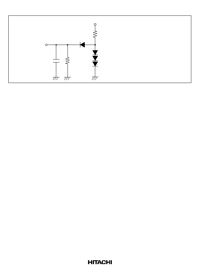
564
Measurement Conditions for AC Characteristics
C
R
H
5 V
R
L
LSI
output pin
C =
Input/output timing measurement levels
Low: 0.8 V
High: 2.0 V
R
L
=
R
H
=
90 pF: Ports 1≠4, 6, 9
30 pF: Ports 5, 8
2.4 k
12 k
Figure 23.3 Output Load Circuit

565
Table 23.10
Timing Conditions of On-Chip Supporting Modules
Condition A: V
CC
= 5.0 V ±10%, V
SS
= 0 V, ¯ = 2.0 MHz to maximum operating frequency,
Ta = ≠20∞C to +75∞C (regular specifications), Ta = ≠40∞C to +85∞C (wide-range
specifications)
Condition B: V
CC
= 4.0 V to 5.5 V, V
SS
= 0 V, ¯ = 2.0 MHz to maximum operating frequency,
Ta = ≠20∞C to +75∞C (regular specifications), Ta = ≠40∞C to +85∞C (wide-range
specifications)
Condition C: V
CC
= 2.7 V to 5.5 V*, V
SS
= 0 V, ¯ = 2.0 MHz to maximum operating frequency,
Ta = ≠20∞C to +75∞C
Condition C
Condition B
Condition A
10 MHz
12 MHz
16 MHz
Test
Item
Symbol
Min
Max
Min
Max
Min
Max
Unit
Conditions
FRT
Timer output delay
time
t
FTOD
--
150
--
100
--
100
ns
Fig. 23.13
Timer input setup
time
t
FTIS
80
--
50
--
50
--
ns
Timer clock input
setup time
t
FTCS
80
--
50
--
50
--
ns
Fig. 23.14
Timer clock pulse
width
t
FTCWH
t
FTCWL
1.5
--
1.5
--
1.5
--
t
cyc
TMR
Timer output delay
time
t
TMOD
--
150
--
100
--
100
ns
Fig. 23.15
Timer reset input
setup time
t
TMRS
80
--
50
--
50
--
ns
Fig. 23.17
Timer clock input
setup time
t
TMCS
80
--
50
--
50
--
ns
Fig. 23.16
Timer clock pulse
width (single edge)
t
TMCWH
1.5
--
1.5
--
1.5
--
t
cyc
Timer clock pulse
width (both edges)
t
TMCWL
2.5
--
2.5
--
2.5
--
t
cyc
PWM
Timer output delay
time
t
PWOD
--
150
--
100
--
100
ns
Fig. 23.18
SCI
Input clock (Async) t
Scyc
4
--
4
--
4
--
t
cyc
Fig. 23.19
cycle
(Sync)
6
--
6
--
6
--
t
cyc
Transmit data delay
time (Sync)
t
TXD
--
200
--
100
--
100
ns
Receive data setup
time (Sync)
t
RXS
150
--
100
--
100
--
ns
Receive data hold
time (Sync)
t
RXH
150
--
100
--
100
--
ns
Input clock pulse
width
t
SCKW
0.4
0.6
0.4
0.6
0.4
0.6
t
Scyc
Fig. 23.20

566
Condition C
Condition B
Condition A
10 MHz
12 MHz
16 MHz
Test
Item
Symbol
Min
Max
Min
Max
Min
Max
Unit
Conditions
Ports
Output data delay
time
t
PWD
--
150
--
100
--
100
ns
Fig. 23.21
Input data setup
time
t
PRS
80
--
50
--
50
--
ns
Input data hold time t
PRH
80
--
50
--
50
--
ns
HIF
CS
/HA
0
setup time
t
HAR
10
--
10
--
10
--
ns
Fig. 23.22
read
CS
/HA
0
hold time
t
HRA
10
--
10
--
10
--
ns
cycle
IOR
pulse width
t
HRPW
220
--
120
--
120
--
ns
HDB delay time
t
HRD
--
200
--
100
--
100
ns
HDB hold time
t
HRF
0
40
0
25
0
25
ns
HIRQ delay time
t
HIRQ
--
200
--
120
--
120
ns
HIF
CS
/HA
0
setup time
t
HAW
10
--
10
--
10
--
ns
Fig. 23.23
write
CS
/HA
0
hold time
t
HWA
10
--
10
--
10
--
ns
cycle
IOW
pulse width
t
HWPW
100
--
60
--
60
--
ns
High-speed GATE
A
20
not uesd
t
HDW
50
--
30
--
30
--
ns
High-speed GATE
A
20
uesd
85
--
55
--
45
--
HDB hold time
t
HWD
25
--
15
--
15
--
ns
GA
20
delay time
t
HGA
--
180
--
90
--
90
ns
Note:
*
In the F-ZTAT LH version, V
CC
= 3.0 V to 5.5 V.

567
Table 23.11
I
2
C Bus Timing
Conditions: V
CC
= 2.7 V to 5.5 V*, V
SS
= 0 V, Ta = ≠20∞C to +75∞C, ¯
5 MHz
Rating
Item
Symbol
Min
Typ
Max
Unit
Test Condition
Note
SCL clock
cycle time
t
SCL
12t
cyc
--
--
ns
Figure 23.24
SCL clock
high pulse
width
t
SCLH
3t
cyc
--
--
ns
SCL clock
low pulse
width
t
SCLL
5t
cyc
--
--
ns
SCL, SDA
rise time
t
Sr
--
--
1000
ns
Normal mode
100 kbit/s (max)
20 + 0.1C
b
--
300
High-speed mode
400 kbit/s (max)
SCL, SDA
fall time
t
Sf
--
--
300
ns
Normal mode
100 kbit/s (max)
20 + 0.1C
b
--
300
High-speed mode
400 kbit/s (max)
SDA bus
free time
t
BUF
5t
cyc
--
--
ns
SCL start
condition
hold time
t
STAH
3t
cyc
--
--
ns
SCL resend
start condition
hold time
t
STAS
3t
cyc
--
--
ns
SDA stop
condition
setup time
t
STOS
3t
cyc
--
--
ns
SDA data
setup time
t
SDAS
0.5t
cyc
--
--
ns
SDA data
hold time
t
SDAH
0
--
--
ns
SDA load
capacitance
C
b
--
--
400
pF
Note:
*
In the F-ZTAT LH version, V
CC
= 3.0 V to 5.5 V.

568
Table 23.12
External clock output delay Timing
Conditions: V
CC
= 2.7 V to 5.5 V
*2
, AV
CC
= 2.7 V to 5.5 V
*2
,
V
SS
= AV
SS
= 0V, Ta = ≠40∞C to +85∞C
Item
Symbol
Min
Max
Unit
Notes
External clock output delay time
t
DEXT
*
1
500
--
µs
Figure 23.25
Notes:
*
1 t
DEXT
includes to
RES
pulse width t
RESW
(10 tcyc).
*
2 In the F-ZTAT LH version, V
CC
= 3.0 V to 5.5 V, AV
CC
= 3.0 V to 5.5 V.

569
23.2.3
A/D Converter Characteristics
Table 23.13 lists the characteristics of the on-chip A/D converter.
Table 23.13
A/D Converter Characteristics
Condition A: V
CC
= 5.0 V ±10%, AV
CC
= 5.0 V ±10%, V
SS
= AV
SS
= 0 V, ¯ = 2.0 MHz to
maximum operating frequency, Ta = ≠20∞C to +75∞C (regular specifications),
Ta = ≠40∞C to +85∞C (wide-range specifications)
Condition B: V
CC
= 4.0 V to 5.5 V, AV
CC
= 4.0 V to 5.5 V, V
SS
= AV
SS
= 0 V, ¯ = 2.0 MHz to
maximum operating frequency, Ta = ≠20∞C to +75∞C (regular specifications),
Ta = ≠40∞C to +85∞C (wide-range specifications)
Condition C: V
CC
= 2.7 V to 5.5 V
*2
, AV
CC
= 2.7 V to 5.5 V
*2
, V
SS
= AV
SS
= 0 V, ¯ = 2.0 MHz to
maximum operating frequency, Ta = ≠20∞C to +75∞C
Condition C
Condition B
Condition A
10 MHz
12 MHz
16 MHz
Item
Min
Typ
Max
Min
Typ
Max
Min
Typ
Max
Unit
Resolution
10
10
10
10
10
10
10
10
10
Bits
Conversion (single mode)
*
1
--
--
13.4
--
--
11.2
--
--
8.4
µs
Analog input capacitance
--
--
20
--
--
20
--
--
20
pF
Allowable signal source
impedance
--
--
5
--
--
10
--
--
10
k
Nonlinearity error
--
--
±6.0
--
--
±3.0
--
--
±3.0
LSB
Offset error
--
--
±4.0
--
--
±3.5
--
--
±3.5
LSB
Full-scale error
--
--
±4.0
--
--
±3.5
--
--
±3.5
LSB
Quantizing error
--
--
±0.5
--
--
±0.5
--
--
±0.5
LSB
Absolute accuracy
--
--
±8.0
--
--
±4.0
--
--
±4.0
LSB
Notes:
*
1 Values at maximum operating frequency
*
2 In the F-ZTAT LH version, V
CC
= 3.0 V to 5.5 V, AV
CC
= 3.0 V to 5.5 V.

570
23.2.4
D/A Converter Characteristics (H8/3337 Series Only)
Table 23.14 lists the characteristics of the on-chip D/A converter.
Table 23.14
D/A Converter Characteristics
Condition A: V
CC
= 5.0 V ±10%, AV
CC
= 5.0 V ±10%, V
SS
= AV
SS
= 0 V, ¯ = 2.0 MHz to
maximum operating frequency, Ta = ≠20∞C to +75∞C (regular specifications),
Ta = ≠40∞C to +85∞C (wide-range specifications)
Condition B: V
CC
= 4.0 V to 5.5 V, AV
CC
= 4.0 V to 5.5 V, V
SS
= AV
SS
= 0 V, ¯ = 2.0 MHz to
maximum operating frequency, Ta = ≠20∞C to +75∞C (regular specifications),
Ta = ≠40∞C to +85∞C (wide-range specifications)
Condition C: V
CC
= 2.7 V to 5.5 V*, AV
CC
= 2.7 V to 5.5 V*, V
SS
= AV
SS
= 0 V, ¯ = 2.0 MHz to
maximum operating frequency, Ta = ≠20∞C to +75∞C
Condition C
Condition B
Condition A
10 MHz
12 MHz
16 MHz
Test
Item
Min
Typ
Max
Min
Typ
Max
Min
Typ
Max Unit Conditions
Resolution
8
8
8
8
8
8
8
8
8
Bits
Conversion time
(settling time)
--
--
10.0
--
--
10.0
10.0 µs
30 pF load
capacitance
Absolute accuracy
--
±2.0 ±3.0
--
±1.0 ±1.5
--
±1.0 ±1.5 LSB 2 M
load
resistance
--
--
±2.0
--
--
±1.0
--
--
±1.0 LSB 4 M
load
resistance
Note:
*
In the F-ZTAT LH version, V
CC
= 3.0 V to 5.5 V, AV
CC
= 3.0 V to 5.5 V.

571
23.2.5
Flash Memory Characteristics (H8/3337SF Only)
Table 23.15 shows the flash memory characteristics.
Table 23.15 Flash Memory Characteristics
Conditions: V
CC
= 5.0 V ± 10%, AV
CC
= 5.0 V ± 10%, V
SS
= AV
SS
= 0 V, T
a
= 0 to +75∞C
Item
Symbol
Min
Typ
Max
Unit
Test
Condition
Programming time
*
1
*
2
*
4
tP
--
10
200
ms/
32 bytes
Erase time
*
1
*
3
*
5
tE
--
100
1200
ms/
block
Reprogramming count
N
WEC
--
--
100
Times
Programming Wait time after
SWE-bit setting
*
1
x
10
--
--
µs
Wait time after
PSU-bit setting
*
1
y
50
--
--
µs
Wait time after
P-bit setting
*
1
*
4
z
150
--
500
µs
Wait time after
P-bit clear
*
1
10
--
--
µs
Wait time after
PSU-bit clear
*
1
10
--
--
µs
Wait time after
PV-bit setting
*
1
4
--
--
µs
Wait time after
dummy write
*
1
2
--
--
µs
Wait time after
PV-bit clear
*
1
4
--
--
µs
Maximum
programming
count
*
1
*
4
*
5
N
--
--
403
Times

572
Item
Symbol
Min
Typ
Max
Unit
Test
Condition
Erase
Wait time after
SWE-bit setting
*
1
x
10
--
--
µs
Wait time after
ESU-bit setting
*
1
y
200
--
--
µs
Wait time after
E-bit setting
*
1
*
6
z
5
--
10
ms
Wait time after
E-bit clear
*
1
10
--
--
µs
Wait time after
ESU-bit clear
*
1
10
--
--
µs
Wait time after
EV-bit setting
*
1
20
--
--
µs
Wait time after
dummy write
*
1
2
--
--
µs
Wait time after
EV-bit clear
*
1
5
--
--
µs
Maximum erase
count
*
1
*
6
*
7
N
--
--
120
Times
tE = 10 ms
Notes:
*
1 Set the times according to the program/erase algorithms.
*
2 Programming time per 32 bytes (Shows the total period for which the P-bit in FLMCR1
is set. It does not include the programming verification time.)
*
3 Block erase time (Shows the total period for which the E-bit in FLMCR1 is set. It does
not include the erase verification time.)
*
4 Maximum programming time (tP (max) = wait time after P-bit setting (z)
◊
maximum
programming count (N))
Set the wait time after P-bit setting (z) to the minimum value of 150 µs when the write
counter in the 32-byte write algorithm is between 1 and 4.
*
5 Number of times when the wait time after P-bit setting (z) = 150 us or 500 µs.
The number of writes should be set according to the actual set value of (z) to allow
programming within the maximum programming time (tP).
*
6 Maximum erase time (tE (max) = Wait time after E-bit setting (z)
◊
maximum erase
count (N))
*
7 Number of times when the wait time after E-bit setting (z) = 10 ms.
The number of erases should be set according to the actual set value of (z) to allow
erasing within the maximum erase time (tE).

573
23.3
Absolute Maximum Ratings (H8/3337SF Low-Voltage Version)
Table 23.16 lists the absolute maximum ratings.
Table 23.16 Absolute Maximum Ratings
Item
Symbol
Rating
Unit
Supply voltage
V
CC
≠0.3 to +7.0
V
Input voltage
Pins other than
port 7
V
in
≠0.3 to V
CC
+ 0.3
V
Port 7
V
in
≠0.3 to AV
CC
+ 0.3
V
Analog supply voltage
AV
CC
≠0.3 to +7.0
V
Analog input voltage
V
AN
≠0.3 to AV
CC
+ 0.3
V
Operating temperature
T
opr
Regular specifications: ≠20 to +75
∞C
Wide-range specifications: ≠40 to +85
∞C
Storage temperature
T
stg
≠55 to +125
∞C
Note:
Exceeding the absolute maximum ratings shown in table 23.16 can permanently destroy
the chip.
*

574
23.4
Electrical Characteristics (H8/3337SF Low-Voltage Version)
23.4.1
DC Characteristics
Table 23.17 lists the DC characteristics. Table 23.18 gives the allowable current output values.
Bus drive characteristics common listed in table 23.19.
Table 23.17 DC Characteristics (3-V Version)
Conditions: V
CC
= 3.0 V to 5.5 V, AV
CC
= 3.0 V to 5.5 V
*1
, V
SS
= AV
SS
= 0 V, Ta = ≠20∞C to
+75∞C (regular specifications), Ta = ≠40∞C to +85∞C (wide-range specifications)
Item
Symbol
Min
Typ
Max
Unit
Test
Conditions
Schmitt
P6
7
to P6
0
*
4
,
(1)
V
T
≠
V
CC
◊
0.15 --
--
V
trigger input
IRQ
2
to
IRQ
0
*
5
,
V
T
+
--
--
V
CC
◊
0.7
voltage
IRQ
7
to IRQ
3
V
T
+
≠ V
T
≠
0.2
--
--
Input high
voltage
RES
,
STBY
,
MD
1
, MD
0
,
EXTAL,
NMI
(2)
V
IH
V
CC
◊
0.9
--
V
CC
+ 0.3
V
SCL, SDA
V
CC
◊
0.7
--
V
CC
+ 0.3
P7
7
to P7
0
V
CC
◊
0.7
--
AV
CC
+ 0.3
All input pins other
than (1) and (2)
above
V
CC
◊
0.7
--
V
CC
+ 0.3
Input low
voltage
*
4
RES
,
STBY
,
MD
1
, MD
0
(3)
V
IL
≠0.3
--
V
CC
◊
0.1
V
SCL, SDA
≠0.3
--
V
CC
◊
0.15
All input pins other
than (1) and (3)
above
≠0.3
--
V
CC
◊
0.15
Output high
All output pins
*
6
V
OH
V
CC
≠ 0.5
--
--
V
I
OH
= ≠200 µA
voltage
V
CC
≠ 1.0
--
--
I
OH
= ≠1 mA
Output low
All output pins
*
6
V
OL
--
--
0.4
V
I
OL
= 0.8 mA
voltage
P1
7
to P1
0
,
P2
7
to P2
0
--
--
0.4
I
OL
= 1.6 mA
Input
RES
,
STBY
| I
in
|
--
--
10.0
µA
Vin = 0.5 V to
leakage
NMI
, MD
1
, MD
0
--
--
1.0
V
CC
≠ 0.5 V
current
P7
7
to P7
0
--
--
1.0
Vin = 0.5 V to
AV
CC
≠ 0.5 V

575
Item
Symbol
Min
Typ
Max
Unit
Test
Conditions
Leakage
current in
three-state
(off state)
Ports 1 to 6, 8, 9
| I
TSI
|
--
--
1.0
µA
Vin = 0.5 V to
V
CC
≠ 0.5 V
Input pull-up Ports 1 to 3
≠I
P
3
--
120
µA
Vin = 0 V,
MOS
current
Ports 6
30
--
250
V
CC
= 3.0 V to
3.6 V
Input
capacitance
RES
,
STBY
(4)
C
in
--
--
60
pF
Vin = 0 V,
F = 1MHz,
Ta = 25∞C
NMI
, MD
1
--
--
50
f = 1 MHz,
P9
7
, P8
6
--
--
20
Ta = 25∞C
All input pins other
than (4) above
--
--
15
Current
dissipation
*
2
Normal
operation
I
CC
--
7
--
mA
f = 6 MHz,
3.0 V to 3.6 V
--
12
22
f = 10 MHz,
V
CC
= 3.0 V to
3.6 V
--
25
--
f = 10 MHz,
V
CC
= 4.0 V to
5.5 V
Sleep mode
--
5
--
f = 6 MHz,
3.0 V to 3.6 V
--
9
16
f = 10 MHz,
V
CC
= 3.0 V to
3.6 V
--
18
--
f = 10 MHz,
V
CC
= 4.0 V to
5.5 V
Standby modes
*
3
--
0.01
5.0
µA
Ta
50∞C
--
--
20.0
50∞C < Ta

576
Item
Symbol
Min
Typ
Max
Unit
Test
Conditions
Analog
supply
During A/D
conversion
AI
CC
--
2.0
5.0
mA
current
During A/D and D/A
conversion
--
2.0
5.0
A/D and D/A
conversion idle
--
0.01
5.0
µA
AV
CC
= 2.0 V
to 5.5 V
Analog supply voltage
*
1
AV
CC
3.0
--
5.5
V
During
operation
2.0
--
5.5
While idle or
when not in
use
RAM standby voltage
V
RAM
2.0
--
--
V
Notes:
*
1 Even when the A/D and D/A converters are not used, connect AV
CC
to power supply V
CC
and keep the applied voltage between 2.0 V and 5.5 V.
*
2 Current dissipation values assume that V
IH min
= V
CC
≠ 0.5 V, V
IL max
= 0.5 V, all output
pins are in the no-load state, and all input pull-up transistors are off.
*
3 For these values it is assumed that V
RAM
V
CC
< 3.0 V and V
IH min
= V
CC
◊
0.9, V
IL max
=
0.3 V.
*
4 P6
7
to P6
0
include supporting module inputs multiplexed with them.
*
5
IRQ
2
includes
ADTRG
multiplexed with it.
*
6 Applies when IICE = 0. The output low level is determined separately when the bus
drive function is selected.
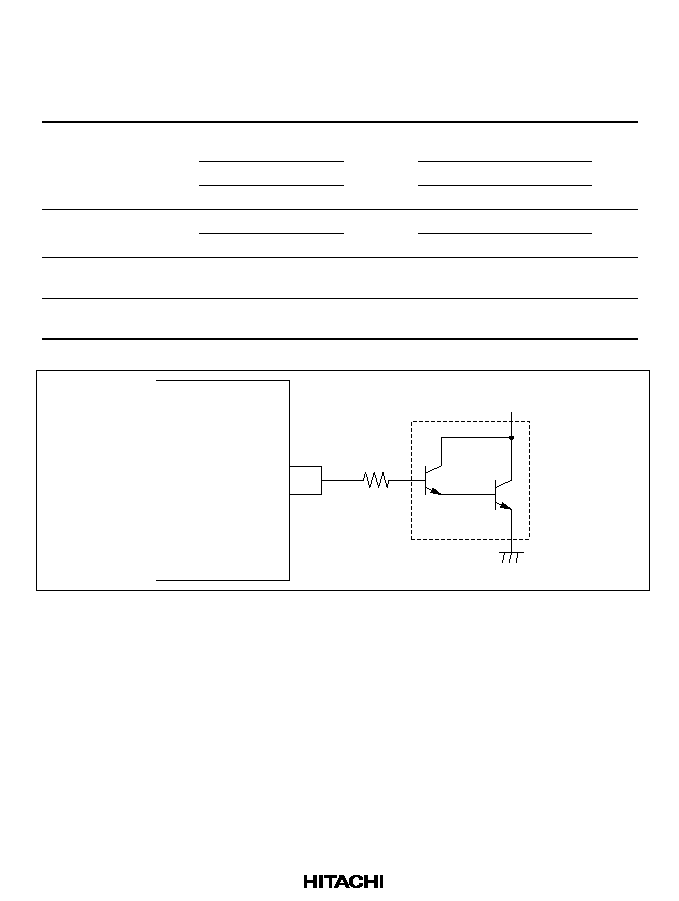
577
Table 23.18 Allowable Output Current Values (3-V Version)
Conditions: V
CC
= 3.0 to 5.5 V, AV
CC
= 3.0 V to 5.5 V, V
SS
= AV
SS
= 0 V, Ta = ≠20∞C to +75∞C
(regular specifications), Ta = ≠40∞C to +85∞C (wide-range specifications)
Item
Symbol
Min
Typ
Max
Unit
Allowable output low
current (per pin)
SCL, SDA
(bus drive selection)
I
OL
--
--
10
mA
Ports 1 and 2
--
--
2
Other output pins
--
--
1
Allowable output low
Ports 1 and 2, total
I
OL
--
--
40
mA
current (total)
Total of all output
--
--
60
Allowable output high
current (per pin)
All output pins
≠I
OH
--
--
2
mA
Allowable output high
current (total)
Total of all output
≠I
OH
--
--
30
mA
H8/3337 Series or
H8/3397 Series
Port
2 k
Darlington
transistor
Figure 23.4 Example of Circuit for Driving a Darlington Transistor (5-V Version)
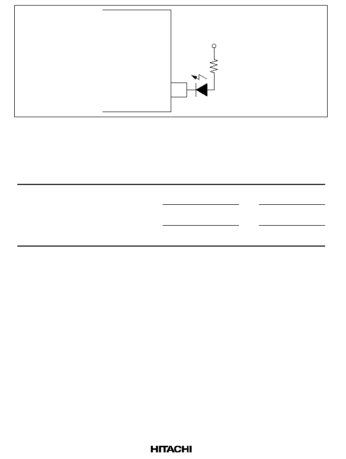
578
H8/3337 Series or
H8/3397 Series
Ports 1 or 2
LED
600
V
CC
Figure 23.5 Example of Circuit for Driving an LED (5-V Version)
Table 23.19 Bus Drive Characteristics
Conditions: V
CC
= 3.0 V to 5.5 V, V
SS
= 0 V, Ta = ≠20∞C to 75∞C
Item
Symbol
Min
Typ
Max
Unit
Test Condition
Output low
voltage
SCL, SDA
(bus drive selection)
V
OL
--
--
0.5
V
V
CC
= 5 V ±10%
I
OL
= 16 mA
--
--
0.5
V
CC
= 3.0 V to 5.5 V
I
OL
= 8 mA
--
--
0.4
V
CC
= 3.0 V to 5.5 V
I
OL
= 3 mA
23.4.2
AC Characteristics
The AC characteristics are listed in following tables. Bus timing parameters are given in table
23.20, control signal timing parameters in table 23.21, timing parameters of the on-chip supporting
modules in table 23.22, I
2
C bus timing parameters in table 23.23, and external clock output delay
timing parameters in table 23.24.

579
Table 23.20 Bus Timing
Conditions: V
CC
= 3.0 V to 5.5 V, V
SS
= 0 V, ¯ = 2.0 MHz to maximum operating frequency,
Ta = ≠20∞C to +75∞C (regular specifications), Ta = ≠40∞C to +85∞C (wide-range
specifications)
Condition
10 MHz
Item
Symbol
Min
Max
Unit
Test Conditions
Clock cycle time
t
cyc
100
500
ns
Fig. 23.7
Clock pulse width low
t
CL
30
--
ns
Clock pulse width high
t
CH
30
--
ns
Clock rise time
t
Cr
--
20
ns
Clock fall time
t
Cf
--
20
ns
Address delay time
t
AD
--
50
ns
Address hold time
t
AH
20
--
ns
Address strobe delay time
t
ASD
--
50
ns
Write strobe delay time
t
WSD
--
50
ns
Strobe delay time
t
SD
--
50
ns
Write strobe pulse width
*
t
WSW
110
--
ns
Address setup time 1
*
t
AS1
15
--
ns
Address setup time 2
*
t
AS2
65
--
ns
Read data setup time
t
RDS
35
--
ns
Read data hold time
*
t
RDH
0
--
ns
Read data access time
*
t
ACC
--
170
ns
Write data delay time
t
WDD
--
75
ns
Write data setup time
t
WDS
5
--
ns
Write data hold time
t
WDH
20
--
ns
Wait setup time
t
WTS
40
--
ns
Fig. 23.8
Wait hold time
t
WTH
10
--
ns
Note:
*
Values at maximum operating frequency
580
Table 23.21 Control Signal Timing
Conditions: V
CC
= 3.0 V to 5.5 V, V
SS
= 0 V, ¯ = 2.0 MHz to maximum operating frequency,
Ta = ≠20∞C to +75∞C (regular specifications), Ta = ≠40∞C to +85∞C (wide-range
specifications)
Condition
10 MHz
Item
Symbol
Min
Max
Unit
Test Conditions
RES
setup time
t
RESS
300
--
ns
Fig. 23.9
RES
pulse width
t
RESW
10
--
t
cyc
NMI
setup time (
NMI
, IRQ
0
to IRQ
7
)
t
NMIS
300
--
ns
Fig. 23.10
NMI
hold time (
NMI
, IRQ
0
to IRQ
7
)
t
NMIH
10
--
ns
Interrupt pulse width for recovery
from software standby mode
(
NMI
, IRQ
0
to IRQ
2
, IRQ
6
)
t
NMIW
300
--
ns
Crystal oscillator settling time
(reset)
t
OSC1
20
--
ms
Fig. 23.11
Crystal oscillator settling time
(software standby)
t
OSC2
8
--
ms
Fig. 23.12
Measurement Conditions for AC Characteristics
C
R
H
5 V
R
L
LSI
output pin
C =
Input/output timing measurement levels
Low: 0.8 V
High: 2.0 V
R
L
=
R
H
=
90 pF: Ports 1≠4, 6, 9
30 pF: Ports 5, 8
2.4 k
12 k
Figure 23.6 Output Load Circuit

581
Table 23.22 Timing Conditions of On-Chip Supporting Modules
Conditions: V
CC
= 3.0 V to 5.5 V, V
SS
= 0 V, ¯ = 2.0 MHz to maximum operating frequency,
Ta = ≠20∞C to +75∞C (regular specifications), Ta = ≠40∞C to +85∞C (wide-range
specifications)
Condition
10 MHz
Item
Symbol
Min
Max
Unit
Test Conditions
FRT
Timer output delay time
t
FTOD
--
150
ns
Fig. 23.13
Timer input setup time
t
FTIS
80
--
ns
Timer clock input setup time
t
FTCS
80
--
ns
Fig. 23.14
Timer clock pulse width
t
FTCWH
1.5
--
t
cyc
t
FTCWL
TMR
Timer output delay time
t
TMOD
--
150
ns
Fig. 23.15
Timer reset input setup time
t
TMRS
80
--
ns
Fig. 23.17
Timer clock input setup time
t
TMCS
80
--
ns
Fig. 23.16
Timer clock pulse width (single
edge)
t
TMCWH
1.5
--
t
cyc
Timer clock pulse width (both
edges)
t
TMCWL
2.5
--
t
cyc
PWM
Timer output delay time
t
PWOD
--
150
ns
Fig. 23.18
SCI
Input clock cycle
(Async)
t
Scyc
4
--
t
cyc
Fig. 23.19
(Sync)
6
--
t
cyc
Transmit data delay time (Sync)
t
TXD
--
200
ns
Receive data setup time (Sync)
t
RXS
150
--
ns
Receive data hold time (Sync)
t
RXH
150
--
ns
Input clock pulse width
t
SCKW
0.4
0.6
t
Scyc
Fig. 23.20
Ports
Output data delay time
t
PWD
--
150
ns
Fig. 23.21
Input data setup time
t
PRS
80
--
ns
Input data hold time
t
PRH
80
--
ns
HIF read
CS
/HA
0
setup time
t
HAR
10
--
ns
Fig. 23.22
cycle
CS
/HA
0
hold time
t
HRA
10
--
ns
IOR
pulse width
t
HRPW
220
--
ns
HDB delay time
t
HRD
--
200
ns
HDB hold time
t
HRF
0
40
ns
HIRQ delay time
t
HIRQ
--
200
ns
HIF write
CS
/HA
0
setup time
t
HAW
10
--
ns
Fig. 23.23
cycle
CS
/HA
0
hold time
t
HWA
10
--
ns
IOW
pulse width
t
HWPW
100
--
ns
High-speed GATE A
20
not uesd
t
HDW
50
--
ns
High-speed GATE A
20
uesd
85
--
HDB hold time
t
HWD
25
--
ns
GA
20
delay time
t
HGA
--
180
ns

582
Table 23.23 I
2
C Bus Timing
Conditions: V
CC
= 3.0 V to 5.5 V, V
SS
= 0 V, Ta = ≠20∞C to +75∞C (regular specifications),
Ta = ≠40∞C to +85∞C (wide-range specifications), ¯ = 5.0 MHz to maximum
operating frequency
Rating
Item
Symbol
Min
Typ
Max
Unit
Test Condition
Note
SCL clock
cycle time
t
SCL
12t
cyc
--
--
ns
Figure 23.24
SCL clock
high pulse
width
t
SCLH
3t
cyc
--
--
ns
SCL clock
low pulse
width
t
SCLL
5t
cyc
--
--
ns
SCL, SDA
rise time
t
Sr
--
--
1000
ns
Normal mode
100 kbit/s (max)
20 + 0.1C
b
--
300
High-speed mode
400 kbit/s (max)
SCL, SDA
fall time
t
Sf
--
--
300
ns
Normal mode
100 kbit/s (max)
20 + 0.1C
b
--
300
High-speed mode
400 kbit/s (max)
SDA bus
free time
t
BUF
5t
cyc
--
--
ns
SCL start
condition
hold time
t
STAH
3t
cyc
--
--
ns
SCL resend
start condition
hold time
t
STAS
3t
cyc
--
--
ns
SDA stop
condition
setup time
t
STOS
3t
cyc
--
--
ns
SDA data
setup time
t
SDAS
0.5t
cyc
--
--
ns
SDA data
hold time
t
SDAH
0
--
--
ns
SDA load
capacitance
C
b
--
--
400
pF

583
23.4.3
A/D Converter Characteristics
Table 23.24 lists the characteristics of the on-chip A/D converter.
Table 23.24 A/D Converter Characteristics
Conditions: V
CC
= 3.0 V to 5.5 V, AV
CC
= 3.0 V to 5.5 V, V
SS
= AV
SS
= 0 V, ¯ = 2.0 MHz to
maximum operating frequency, Ta = ≠20∞C to +75∞C (regular specifications),
Ta = ≠40∞C to +85∞C (wide-range specifications)
Condition
10 MHz
Item
Min
Typ
Max
Unit
Resolution
10
10
10
Bits
Conversion (single mode)
*
--
--
13.4
µs
Analog input capacitance
--
--
20
pF
Allowable signal source impedance
--
--
5
k
Nonlinearity error
--
--
±6.0
LSB
Offset error
--
--
±4.0
LSB
Full-scale error
--
--
±4.0
LSB
Quantizing error
--
--
±0.5
LSB
Absolute accuracy
--
--
±8.0
LSB
Note:
*
Values at maximum operating frequency

584
23.4.4
D/A Converter Characteristics (H8/3337 Series Only)
Table 23.25 lists the characteristics of the on-chip D/A converter.
Table 23.25 D/A Converter Characteristics
Conditions: V
CC
= 3.0 V to 5.5 V, AV
CC
= 3.0 V to 5.5 V, V
SS
= AV
SS
= 0 V, ¯ = 2.0 MHz to
maximum operating frequency, Ta = ≠20∞C to +75∞C (regular specifications),
Ta = ≠40∞C to +85∞C (wide-range specifications)
Condition
10 MHz
Item
Min
Typ
Max
Unit
Test Conditions
Resolution
8
8
8
Bits
Conversion time (settling time)
--
--
10.0
µs
30 pF load capacitance
Absolute accuracy
--
±2.0
±3.0
LSB
2 M
load resistance
--
--
±2.0
LSB
4 M
load resistance

585
23.4.5
Flash Memory Characteristics
Table 23.26 shows the flash memory characteristics.
Table 23.26 Flash Memory Characteristics
Conditions: V
CC
= 3.0 V to 3.6 V, AV
CC
= 3.0 V to 5.5 V, V
SS
= AV
SS
= 0 V, T
a
= 0 to +75∞C
Item
Symbol
Min
Typ
Max
Unit
Test
Condition
Programming time
*
1
*
2
*
4
tP
--
10
200
ms/
32 bytes
Erase time
*
1
*
3
*
5
tE
--
100
1200
ms/
block
Reprogramming count
N
WEC
--
--
100
Times
Programming Wait time after
SWE-bit setting
*
1
x
10
--
--
µs
Wait time after
PSU-bit setting
*
1
y
50
--
--
µs
Wait time after
P-bit setting
*
1
*
4
z
150
--
500
µs
Wait time after
P-bit clear
*
1
10
--
--
µs
Wait time after
PSU-bit clear
*
1
10
--
--
µs
Wait time after
PV-bit setting
*
1
4
--
--
µs
Wait time after
dummy write
*
1
2
--
--
µs
Wait time after
PV-bit clear
*
1
4
--
--
µs
Maximum
programming
count
*
1
*
4
*
5
N
--
--
403
Times

586
Item
Symbol
Min
Typ
Max
Unit
Test
Condition
Erase
Wait time after
SWE-bit setting
*
1
x
10
--
--
µs
Wait time after
ESU-bit setting
*
1
y
200
--
--
µs
Wait time after
E-bit setting
*
1
*
6
z
5
--
10
ms
Wait time after
E-bit clear
*
1
10
--
--
µs
Wait time after
ESU-bit clear
*
1
10
--
--
µs
Wait time after
EV-bit setting
*
1
20
--
--
µs
Wait time after
dummy write
*
1
2
--
--
µs
Wait time after
EV-bit clear
*
1
5
--
--
µs
Maximum erase
count
*
1
*
6
*
7
N
--
--
120
Times
tE = 10 ms
Notes:
*
1 Set the times according to the program/erase algorithms.
*
2 Programming time per 32 bytes (Shows the total period for which the P-bit in FLMCR1
is set. It does not include the programming verification time.)
*
3 Block erase time (Shows the total period for which the E-bit in FLMCR1 is set. It does
not include the erase verification time.)
*
4 Maximum programming time (tP (max) = wait time after P-bit setting (z)
◊
maximum
programming count (N))
Set the wait time after P-bit setting (z) to the minimum value of 150 µs when the write
counter in the 32-byte write algorithm is between 1 and 4.
*
5 Number of times when the wait time after P-bit setting (z) = 150 µs or 500 µs.
The number of writes should be set according to the actual set value of (z) to allow
programming within the maximum programming time (tP).
*
6 Maximum erase time (tE (max) = Wait time after E-bit setting (z)
◊
maximum erase
count (N))
*
7 Number of times when the wait time after E-bit setting (z) = 10 ms.
The number of erases should be set according to the actual set value of (z) to allow
erasing within the maximum erase time (tE).
587
23.5
MCU Operational Timing
This section provides the following timing charts:
23.5.1
Bus Timing
Figures 23.7 and 23.8
23.5.2
Control Signal Timing
Figures 23.9 to 23.12
23.5.3
16-Bit Free-Running Timer Timing
Figures 23.13 and 23.14
23.5.4
8-Bit Timer Timing
Figures 23.15 to 23.17
23.5.5
PWM Timer Timing
Figure 23.18
23.5.6
SCI Timing
Figures 23.19 and 23.20
23.5.7
I/O Port Timing
Figure 23.21
23.5.8
Host Interface Timing (H8/3337 Series Only)
Figures 23.22 and 23.23
23.5.9
I
2
C Bus Timing (Option) (H8/3337 Series Only) Figure 23.24
23.5.10 External Clock Output Timing
Figure 23.25
23.5.1
Bus Timing
(1) Basic Bus Cycle (without Wait States) in Expanded Modes
T
2
T
1
t
cyc
T
3
t
CH
t
CL
t
AD
t
Cr
t
ASD
t
ACC
t
RDS
t
WSD
t
AS2
t
WDD
t
WDS
t
WDH
t
AH
t
WSW
t
RDH
t
AH
t
SD
¯
A
15
to A
0
WR
D
7
to D
0
(read)
D
7
to D
0
(write)
AS
,
RD
t
Cf
t
AS1
t
SD
Figure 23.7 Basic Bus Cycle (without Wait States) in Expanded Modes

588
(2) Basic Bus Cycle (with 1 Wait State) in Expanded Modes
¯
AS
,
RD
WR
WAIT
D
7
to D
0
(read)
A
15
to A
0
D
7
to D
0
(write)
T
1
T
2
T
W
T
3
t
WTS
t
WTH
t
WTS
t
WTH
Figure 23.8 Basic Bus Cycle (with 1 Wait State) in Expanded Modes (Modes 1 and 2)
23.5.2
Control Signal Timing
(1) Reset Input Timing
¯
RES
t
RESS
t
RESS
t
RESW
Figure 23.9 Reset Input Timing

589
(2) Interrupt Input Timing
¯
IRQ
L
NMI
IRQ
i
t
NMIS
t
NMIH
t
NMIS
NMI
IRQ
E
t
NMIW
Note: i = 0 to 7;
IRQ
E
:
IRQ
i
when edge-sensed;
IRQ
L
:
IRQ
i
when level-sensed
Figure 23.10 Interrupt Input Timing
(3) Clock Settling Timing
¯
V
CC
RES
STBY
t
OSC1
t
OSC1
Figure 23.11 Clock Settling Timing

590
(4) Clock Settling Timing for Recovery from Software Standby Mode
¯
NMI
IRQ
i
(i = 0, 1, 2, 6)
t
OSC2
Figure 23.12 Clock Settling Timing for Recovery from Software Standby Mode
23.5.3
16-Bit Free-Running Timer Timing
(1) Free-Running Timer Input/Output Timing
¯
Compare-match
FTIA, FTIB,
FTIC, FTID
FTOA , FTOB
Free-running
timer counter
t
FTOD
t
FTIS
Figure 23.13 Free-Running Timer Input/Output Timing
591
(2) External Clock Input Timing for Free-Running Timer
¯
FTCI
t
FTCS
t
FTCWL
t
FTCWH
Figure 23.14 External Clock Input Timing for Free-Running Timer
23.5.4
8-Bit Timer Timing
(1) 8-Bit Timer Output Timing
¯
Timer
counter
Compare-match
TMO
0
,
TMO
1
t
TMOD
Figure 23.15 8-Bit Timer Output Timing
(2) 8-Bit Timer Clock Input Timing
¯
t
TMCS
t
TMCS
t
TMCWL
t
TMCWH
TMCI
0
,
TMCI
1
Figure 23.16 8-Bit Timer Clock Input Timing

592
(3) 8-Bit Timer Reset Input Timing
N
H'00
¯
Timer
counter
t
TMRS
TMRI
0
,
TMRI
1
Figure 23.17 8-Bit Timer Reset Input Timing
23.5.5
Pulse Width Modulation Timer Timing
Compare-match
t
PWOD
¯
Timer
counter
PW
0
, PW
1
Figure 23.18 PWM Timer Output Timing

593
23.5.6
Serial Communication Interface Timing
(1) SCI Input/Output Timing
t
Scyc
t
TXD
t
RXS
t
RXH
Serial clock
(SCK
0
, SCK
1
)
Transmit
data
(TxD
0
, TxD
1
)
Receive
data
(RxD
0
, RxD
1
)
Figure 23.19 SCI Input/Output Timing (Synchronous Mode)
(2) SCI Input Clock Timing
t
SCKW
t
Scyc
SCK
0
, SCK
1
Figure 23.20 SCI Input Clock Timing
594
23.5.7
I/O Port Timing
Note:
*
Except P9
6
and P7
7
to P7
0
t
PRS
t
PRH
t
PWD
Port 1 to
port 9 (input)
¯
Port 1
*
to
port 9 (output)
T
1
T
2
T
3
Figure 23.21 I/O Port Input/Output Timing
23.5.8
Host Interface Timing (H8/3337 Series Only)
(1) Host Interface Read Timing
CS
/HA
0
HA
0
IOR
HDB
7
to HDB
0
HIRQ
i
(i = 1, 11, 12)
Note: The rising edge timing is the same as port 4 output timing. Refer to figure 23.21.
t
HAR
t
HRPW
t
HRA
t
HRF
t
HRD
t
HIRQ
Effective data
Figure 23.22 Host Interface Read Timing
595
(2) Host Interface Write Timing
CS
/HA
0
HA
0
IOW
HDB
7
to HDB
0
GA
20
t
HAW
t
HWPW
t
HWA
t
HWD
t
HGA
t
HDW
Figure 23.23 Host Interface Write Timing
23.5.9
I
2
C Bus Timing (Option) (H8/3337 Series Only)
SDA
V
IL
V
IH
t
BUF
P
*
S
*
t
STAH
t
SCLH
t
Sr
t
SCLL
t
SCL
t
Sf
t
SDAH
Sr
*
t
SDAS
t
STAS
t
SP
t
STOS
Note:
*
S, P, and Sr are defined as follows:
S:
P:
Sr:
Start condition
Stop condition
Retransmission start condition
SCL
P
*
Figure 23.24 I
2
C Interface Input/Output Timing
596
23.5.10
External Clock Output Timing
V
CC
STBY
V
IH
EXTAL
Note:
*
t
DEXT
includes an
RES
pulse width (t
RESW
) of 10 t
cyc
.
RES
¯
t
DEXT
*
(internal or
external)
Figure 23.25 External clock output delay Timing

597
Appendix A CPU Instruction Set
A.1
Instruction Set List
Operation Notation
Rd8/16
General register (destination) (8 or 16 bits)
Rs8/16
General register (source) (8 or 16 bits)
Rn8/16
General register (8 or 16 bits)
CCR
Condition code register
N
N (negative) flag in CCR
Z
Z (zero) flag in CCR
V
V (overflow) flag in CCR
C
C (carry) flag in CCR
PC
Program counter
SP
Stack pointer
#xx:3/8/16
Immediate data (3, 8, or 16 bits)
d:8/16
Displacement (8 or 16 bits)
@aa:8/16
Absolute address (8 or 16 bits)
+
Addition
≠
Subtraction
◊
Multiplication
˜
Division
Logical AND
Logical OR
Exclusive logical OR
Move
--
NOT (logical complement)
Condition Code Notation
Modified according to the instruction result
*
Undetermined (unpredictable)
0
Always cleared to 0
--
Not affected by the instruction result

598
Table A.1
Instruction Set
Mnemonic
Operation
Addressing Mode/
Instruction Length
Operand Size
#xx: 8/16
Rn
@Rn
@(d:16, Rn)
@≠Rn/@Rn+
@aa: 8/16
@(d:8, PC)
@@aa
Implied
No. of States
I
H N Z V C
Condition Code
MOV.B #xx:8, Rd
MOV.B Rs, Rd
MOV.B @Rs, Rd
MOV.B @(d:16, Rs), Rd
MOV.B @Rs+, Rd
MOV.B @aa:8, Rd
MOV.B @aa:16, Rd
MOV.B Rs, @Rd
MOV.B Rs, @(d:16, Rd)
MOV.B Rs, @≠Rd
MOV.B Rs, @aa:8
MOV.B Rs, @aa:16
MOV.W #xx:16, Rd
MOV.W Rs, Rd
MOV.W @Rs, Rd
MOV.W @(d:16, Rs), Rd
MOV.W @Rs+, Rd
MOV.W @aa:16, Rd
MOV.W Rs, @Rd
MOV.W Rs, @(d:16, Rd)
MOV.W Rs, @≠Rd
MOV.W Rs, @aa:16
POP Rd
PUSH Rs
#xx:8
Rd8
Rs8
Rd8
@Rs16
Rd8
@(d:16, Rs16)
Rd8
@Rs16
Rd8
Rs16+1
Rs16
@aa:8
Rd8
@aa:16
Rd8
Rs8
@Rd16
Rs8
@(d:16, Rd16)
Rd16≠1
Rd16
Rs8
@Rd16
Rs8
@aa:8
Rs8
@aa:16
#xx:16
Rd
Rs16
Rd16
@Rs16
Rd16
@(d:16, Rs16)
Rd16
@Rs16
Rd16
Rs16+2
Rs16
@aa:16
Rd16
Rs16
@Rd16
Rs16
@(d:16, Rd16)
Rd16≠2
Rd16
Rs16
@Rd16
Rs16
@aa:16
@SP
Rd16
SP+2
SP
SP≠2
SP
Rs16
@SP
B
B
B
B
B
B
B
B
B
B
B
B
W
W
W
W
W
W
W
W
W
W
W
W
2
--
--
--
--
--
--
--
--
--
--
--
--
--
--
--
--
--
--
--
--
--
--
--
--
--
--
--
--
--
--
--
--
--
--
--
--
--
--
--
--
--
--
--
--
--
--
--
--
0
0
0
0
0
0
0
0
0
0
0
0
0
0
0
0
0
0
0
0
0
0
0
0
--
--
--
--
--
--
--
--
--
--
--
--
--
--
--
--
--
--
--
--
--
--
--
--
2
2
4
6
6
4
6
4
6
6
4
6
4
2
4
6
6
6
4
6
6
6
6
6
2
2
4
2
2
4
2
4
2
2
4
4
2
2
4
2
4
2
4
2
4
2
2
599
Mnemonic
Operation
Addressing Mode/
Instruction Length
Operand Size
#xx: 8/16
Rn
@Rn
@(d:16, Rn)
@≠Rn/@Rn+
@aa: 8/16
@(d:8, PC)
@@aa
Implied
No. of States
I
H N Z V C
Condition Code
MOVFPE @aa:16, Rd
MOVTPE Rs, @aa:16
EEPMOV
ADD.B #xx:8, Rd
ADD.B Rs, Rd
ADD.W Rs, Rd
ADDX.B #xx:8, Rd
ADDX.B Rs, Rd
ADDS.W #1, Rd
ADDS.W #2, Rd
INC.B Rd
DAA.B Rd
SUB.B Rs, Rd
SUB.W Rs, Rd
SUBX.B #xx:8, Rd
SUBX.B Rs, Rd
SUBS.W #1, Rd
SUBS.W #2, Rd
DEC.B Rd
DAS.B Rd
NEG.B Rd
CMP.B #xx:8, Rd
CMP.B Rs, Rd
CMP.W Rs, Rd
MULXU.B Rs, Rd
if R4L
0 then
Repeat @R5
@R6
R5+1
R5
R6+1
R6
R4L≠1
R4L
Until R4L=0
else next
Rd8+#xx:8
Rd8
Rd8+Rs8
Rd8
Rd16+Rs16
Rd16
Rd8+#xx:8 +C
Rd8
Rd8+Rs8 +C
Rd8
Rd16+1
Rd16
Rd16+2
Rd16
Rd8+1
Rd8
Rd8 decimal adjust
Rd8
Rd8≠Rs8
Rd8
Rd16≠Rs16
Rd16
Rd8≠#xx:8 ≠C
Rd8
Rd8≠Rs8 ≠C
Rd8
Rd16≠1
Rd16
Rd16≠2
Rd16
Rd8≠1
Rd8
Rd8 decimal adjust
Rd8
0≠Rd
Rd
Rd8≠#xx:8
Rd8≠Rs8
Rd16≠Rs16
Rd8
◊
Rs8
Rd16
--
B
B
W
B
B
W
W
B
B
B
W
B
B
W
W
B
B
B
B
B
W
B
B
B
Not supported
Not supported
(5)
(5)
(4)
2
2
2
2
2
2
2
2
2
2
2
2
2
2
2
2
2
2
2
2
2
14
4 -- --
-- --
-- --
2
2
2
2
2
2
2
2
2
2
2
2
2
2
2
2
2
2
2
2
2
2
--
--
--
--
--
--
--
--
--
--
--
--
--
--
--
--
--
--
--
--
--
--
(1)
(2)
(2)
-- -- -- -- --
-- -- -- -- --
--
--
*
*
(3)
(1)
(2)
(2)
-- -- -- -- --
-- -- -- -- --
--
--
*
*
--
(1)
-- -- -- -- --

600
Mnemonic
Operation
Addressing Mode/
Instruction Length
Operand Size
#xx: 8/16
Rn
@Rn
@(d:16, Rn)
@≠Rn/@Rn+
@aa: 8/16
@(d:8, PC)
@@aa
Implied
No. of States
I
H N Z V C
Condition Code
DIVXU.B Rs, Rd
AND.B #xx:8, Rd
AND.B Rs, Rd
OR.B #xx:8, Rd
OR.B Rs, Rd
XOR.B #xx:8, Rd
XOR.B Rs, Rd
NOT.B Rd
SHAL.B Rd
SHAR.B Rd
SHLL.B Rd
SHLR.B Rd
ROTXL.B Rd
ROTXR.B Rd
ROTL.B Rd
ROTR.B Rd
Rd16
˜
Rs8
Rd16
(RdH: remainder,
RdL: quotient)
Rd8
#xx:8
Rd8
Rd8
Rs8
Rd8
Rd8
#xx:8
Rd8
Rd8
Rs8
Rd8
Rd8
#xx:8
Rd8
Rd8
Rs8
Rd8
Rd
Rd
B
B
B
B
B
B
B
B
B
B
B
B
B
B
B
B
2
2
2
2
2
2
2
2
2
2
2
2
2
2
2
2
--
--
--
--
--
--
--
--
--
--
--
--
--
--
--
--
--
--
--
--
--
--
--
--
--
--
--
--
--
--
--
--
(6)
0
(7) --
0
0
0
0
0
0
0
0
0
0
0
0
0
0
--
--
--
--
--
--
--
--
14
2
2
2
2
2
2
2
2
2
2
2
2
2
2
2
b
7
b
0
0
C
b
7
b
0
0
C
C
b
7
b
0
b
7
b
0
0
C
C
b
7
b
0
C
b
7
b
0
C
b
7
b
0
C
b
7
b
0
601
Mnemonic
Operation
Addressing Mode/
Instruction Length
Operand Size
#xx: 8/16
Rn
@Rn
@(d:16, Rn)
@≠Rn/@Rn+
@aa: 8/16
@(d:8, PC)
@@aa
Implied
No. of States
I
H N Z V C
Condition Code
BSET #xx:3, Rd
BSET #xx:3, @Rd
BSET #xx:3, @aa:8
BSET Rn, Rd
BSET Rn, @Rd
BSET Rn, @aa:8
BCLR #xx:3, Rd
BCLR #xx:3, @Rd
BCLR #xx:3, @aa:8
BCLR Rn, Rd
BCLR Rn, @Rd
BCLR Rn, @aa:8
BNOT #xx:3, Rd
BNOT #xx:3, @Rd
BNOT #xx:3, @aa:8
BNOT Rn, Rd
BNOT Rn, @Rd
BNOT Rn, @aa:8
BTST #xx:3, Rd
BTST #xx:3, @Rd
BTST #xx:3, @aa:8
BTST Rn, Rd
BTST Rn, @Rd
BTST Rn, @aa:8
(#xx:3 of Rd8)
1
(#xx:3 of @Rd16)
1
(#xx:3 of @aa:8)
1
(Rn8 of Rd8)
1
(Rn8 of @Rd16)
1
(Rn8 of @aa:8)
1
(#xx:3 of Rd8)
0
(#xx:3 of @Rd16)
0
(#xx:3 of @aa:8)
0
(Rn8 of Rd8)
0
(Rn8 of @Rd16)
0
(Rn8 of @aa:8)
0
(#xx:3 of Rd8)
(
#xx:3 of Rd8
)
(#xx:3 of @Rd16)
(
#xx:3 of @Rd16
)
(#xx:3 of @aa:8)
(
#xx:3 of @aa:8
)
(Rn8 of Rd8)
(
Rn8 of Rd8
)
(Rn8 of @Rd16)
(
Rn8 of @Rd16
)
(Rn8 of @aa:8)
(
Rn8 of @aa:8
)
(
#xx:3 of Rd8
)
Z
(
#xx:3 of @Rd16
)
Z
(
#xx:3 of @aa:8
)
Z
(
Rn8 of Rd8
)
Z
(
Rn8 of @Rd16
)
Z
(
Rn8 of @aa:8
)
Z
B
B
B
B
B
B
B
B
B
B
B
B
B
B
B
B
B
B
B
B
B
B
B
B
2
2
2
2
2
2
2
2
4
4
4
4
4
4
4
4
4
4
4
4
4
4
4
4
--
--
--
--
--
--
--
--
--
--
--
--
--
--
--
--
--
--
--
--
--
--
--
--
--
--
--
--
--
--
--
--
--
--
--
--
--
--
--
--
--
--
--
--
--
--
--
--
--
--
--
--
--
--
--
--
--
--
--
--
--
--
--
--
--
--
--
--
--
--
--
--
--
--
--
--
--
--
--
--
--
--
--
--
--
--
--
--
--
--
--
--
--
--
--
--
--
--
--
--
--
--
--
--
--
--
--
--
--
--
--
--
--
--
--
--
--
--
--
--
--
--
--
--
--
--
--
--
--
--
--
--
--
--
--
--
--
--
2
8
8
2
8
8
2
8
8
2
8
8
2
8
8
2
8
8
2
6
6
2
6
6

602
Mnemonic
Operation
Addressing Mode/
Instruction Length
Operand Size
#xx: 8/16
Rn
@Rn
@(d:16, Rn)
@≠Rn/@Rn+
@aa: 8/16
@(d:8, PC)
@@aa
Implied
No. of States
I
H N Z V C
Condition Code
BLD #xx:3, Rd
BLD #xx:3, @Rd
BLD #xx:3, @aa:8
BILD #xx:3, Rd
BILD #xx:3, @Rd
BILD #xx:3, @aa:8
BST #xx:3, Rd
BST #xx:3, @Rd
BST #xx:3, @aa:8
BIST #xx:3, Rd
BIST #xx:3, @Rd
BIST #xx:3, @aa:8
BAND #xx:3, Rd
BAND #xx:3, @Rd
BAND #xx:3, @aa:8
BIAND #xx:3, Rd
BIAND #xx:3, @Rd
BIAND #xx:3, @aa:8
BOR #xx:3, Rd
BOR #xx:3, @Rd
BOR #xx:3, @aa:8
BIOR #xx:3, Rd
BIOR #xx:3, @Rd
BIOR #xx:3, @aa:8
BXOR #xx:3, Rd
BXOR #xx:3, @Rd
BXOR #xx:3, @aa:8
BIXOR #xx:3, Rd
(#xx:3 of Rd8)
C
(#xx:3 of @Rd16)
C
(#xx:3 of @aa:8)
C
(
#xx:3 of Rd8
)
C
(
#xx:3 of @Rd16
)
C
(
#xx:3 of @aa:8
)
C
C
(#xx:3 of Rd8)
C
(#xx:3 of @Rd16)
C
(#xx:3 of @aa:8)
C
(#xx:3 of Rd8)
C
(#xx:3 of @Rd16)
C
(#xx:3 of @aa:8)
C
(#xx:3 of Rd8)
C
C
(#xx:3 of @Rd16)
C
C
(#xx:3 of @aa:8)
C
C
(
#xx:3 of Rd8
)
C
C
(
#xx:3 of @Rd16
)
C
C
(
#xx:3 of @aa:8
)
C
C
(#xx:3 of Rd8)
C
C
(#xx:3 of @Rd16)
C
C
(#xx:3 of @aa:8)
C
C
(
#xx:3 of Rd8
)
C
C
(
#xx:3 of @Rd16
)
C
C
(
#xx:3 of @aa:8
)
C
C
(#xx:3 of Rd8)
C
C
(#xx:3 of @Rd16)
C
C
(#xx:3 of @aa:8)
C
C
(
#xx:3 of Rd8
)
C
B
B
B
B
B
B
B
B
B
B
B
B
B
B
B
B
B
B
B
B
B
B
B
B
B
B
B
B
2
2
2
2
2
2
2
2
2
2
4
4
4
4
4
4
4
4
4
4
4
4
4
4
4
4
4
4
--
--
--
--
--
--
--
--
--
--
--
--
--
--
--
--
--
--
--
--
--
--
--
--
--
--
--
--
--
--
--
--
--
--
--
--
--
--
--
--
--
--
--
--
--
--
--
--
--
--
--
--
--
--
--
--
--
--
--
--
--
--
--
--
--
--
--
--
--
--
--
--
--
--
--
--
--
--
--
--
--
--
--
--
--
--
--
--
--
--
--
--
--
--
--
--
--
--
--
--
--
--
--
--
--
--
--
--
--
--
--
--
--
--
--
--
--
--
--
--
--
--
--
--
--
--
--
--
--
--
--
--
--
--
--
--
--
--
--
--
--
--
--
--
--
--
2
6
6
2
6
6
2
8
8
2
8
8
2
6
6
2
6
6
2
6
6
2
6
6
2
6
6
2

603
Mnemonic
Operation
Addressing Mode/
Instruction Length
Operand Size
#xx: 8/16
Rn
@Rn
@(d:16, Rn)
@≠Rn/@Rn+
@aa: 8/16
@(d:8, PC)
@@aa
Implied
No. of States
I
H N Z V C
Condition Code
BIXOR #xx:3, @Rd
BIXOR #xx:3, @aa:8
BRA d:8 (BT d:8)
BRN d:8 (BF d:8)
BHI d:8
BLS d:8
BCC d:8 (BHS d:8)
BCS d:8 (BLO d:8)
BNE d:8
BEQ d:8
BVC d:8
BVS d:8
BPL d:8
BMI d:8
BGE d:8
BLT d:8
BGT d:8
BLE d:8
JMP @Rn
JMP @aa:16
JMP @@aa:8
BSR d:8
JSR @Rn
JSR @aa:16
C
(
#xx:3 of @Rd16
)
C
C
(
#xx:3 of @aa:8
)
C
PC
PC+d:8
PC
PC+2
If
condition
is true
then
PC
PC+d:8
else next;
B
B
--
--
--
--
--
--
--
--
--
--
--
--
--
--
--
--
--
--
--
--
--
--
4
2
2
4
4
4
2
2
2
2
2
2
2
2
2
2
2
2
2
2
2
2
2
2
--
--
--
--
--
--
--
--
--
--
--
--
--
--
--
--
--
--
--
--
--
--
--
--
--
--
--
--
--
--
--
--
--
--
--
--
--
--
--
--
--
--
--
--
--
--
--
--
--
--
--
--
--
--
--
--
--
--
--
--
--
--
--
--
--
--
--
--
--
--
--
--
--
--
--
--
--
--
--
--
--
--
--
--
--
--
--
--
--
--
--
--
--
--
--
--
--
--
--
--
--
--
--
--
--
--
--
--
--
--
--
--
--
--
--
--
--
--
--
--
--
--
--
--
--
--
--
--
--
--
--
--
--
--
--
--
--
--
--
--
--
--
6
6
4
4
4
4
4
4
4
4
4
4
4
4
4
4
4
4
4
6
8
6
6
8
C
Z = 0
C
Z = 1
C = 0
C = 1
Z = 0
Z = 1
V = 0
V = 1
N = 0
N = 1
N
V = 0
N
V = 1
Z
(N
V) = 0
Z
(N
V) = 1
PC
Rn16
PC
aa:16
PC
@aa:8
SP≠2
SP
PC
@SP
PC
PC+d:8
SP≠2
SP
PC
@SP
PC
Rn16
SP≠2
SP
PC
@SP
PC
aa:16
Branching
Condition

604
Mnemonic
Operation
Addressing Mode/
Instruction Length
Operand Size
#xx: 8/16
Rn
@Rn
@(d:16, Rn)
@≠Rn/@Rn+
@aa: 8/16
@(d:8, PC)
@@aa
Implied
No. of States
I
H N Z V C
Condition Code
JSR @@aa:8
RTS
RTE
SLEEP
LDC #xx:8, CCR
LDC Rs, CCR
STC CCR, Rd
ANDC #xx:8, CCR
ORC #xx:8, CCR
XORC #xx:8, CCR
NOP
SP≠2
SP
PC
@SP
PC
@aa:8
PC
@SP
SP+2
SP
CCR
@SP
SP+2
SP
PC
@SP
SP+2
SP
Transition to power-down
state.
#xx:8
CCR
Rs8
CCR
CCR
Rd8
CCR
#xx:8
CCR
CCR
#xx:8
CCR
CCR
#xx:8
CCR
PC
PC+2
--
--
--
--
B
B
B
B
B
B
--
2
-- -- -- -- -- -- 8
8
10
2
2
2
2
2
2
2
2
2
2
2 -- -- -- -- -- --
2
2
2
-- -- -- -- -- --
2
2
2
2 -- -- -- -- -- --
-- -- -- -- -- --
Notes: The number of states is the number of states required for execution when the instruction
and its operands are located in on-chip memory.
(1) Set to 1 when there is a carry or borrow from bit 11; otherwise cleared to 0.
(2) If the result is zero, the previous value of the flag is retained; otherwise the flag is
cleared to 0.
(3) Set to 1 if decimal adjustment produces a carry; otherwise retains its previous value.
(4) The number of states required for execution is 4n+8 (n = value of R4L).
(5) These instructions are not supported by the H8/3337 Series and H8/3397 Series.
(6) Set to 1 if the divisor is negative; otherwise cleared to 0.
(7) Set to 1 if the divisor is 0; otherwise cleared to 0.

605
A.2
Operation Code Map
Table A.2 is a map of the operation codes contained in the first byte of the instruction code (bits
15 to 8 of the first instruction word).
Some pairs of instructions have identical first bytes. These instructions are differentiated by the
first bit of the second byte (bit 7 of the first instruction word).
Instruction when first bit of byte 2 (bit 7 of first instruction word) is 0.
Instruction when first bit of byte 2 (bit 7 of first instruction word) is 1.

606
Table A.2
Operation Code Map
;;
;
;
;;
;
High
Low
0123
4567
89
A
B
C
D
E
F
0
1
2
3
4
5
6
7
8
9
A
B
C
D
E
F
NOP
BRA
*
2
MULXU
BSET
SHLL
SHAL
SLEEP
BRN
*
2
DIVXU
BNOT
SHLR
SHAR
STC
BHI
BCLR
ROTXL
ROTL
LDC
BLS
BTS
ROTXR
ROTR
ORC
OR
BCC
*
2
RTS
XORC
XOR
BCS
*
2
BSR
BOR
BIOR
BXOR
BIXOR
BAND
BIAND
ANDC
AND
BNE
RTE
LDC
BEQ
NOT
NEG
BLD
BILD
BST
BIST
ADD
SUB
BVC
BVS
MOV
INC
DEC
BPL
JMP
ADDS
SUBS
BMI
EEPMOV
MOV
CMP
BGE
BLT
ADDX
SUBX
BGT
JSR
DAA
DAS
BLE
MOV
ADD
ADDX
CMP
SUBX
OR
XOR
AND
MOV
MOV
*
1
;
Notes:
*
1
*
2
Bit manipulation instructions
The MOVFPE and MOVTPE instructions are identical to MOV instructions in the first byte and first bit of the second byte (bits 1
5 to 7 of the instruction word).
The PUSH and POP instructions are identical in machine language to MOV instructions.
The BT, BF, BHS, and BLO instructions are identical in machine language to BRA, BRN, BCC, and BCS, respectively.

607
A.3
Number of States Required for Execution
The tables below can be used to calculate the number of states required for instruction execution.
Table A.3 indicates the number of states required for each cycle (instruction fetch, branch address
read, stack operation, byte data access, word data access, internal operation). Table A.4 indicates
the number of cycles of each type occurring in each instruction. The total number of states
required for execution of an instruction can be calculated from these two tables as follows:
Execution states = I
◊
S
I
+ J
◊
S
J
+ K
◊
S
K
+ L
◊
S
L
+ M
◊
S
M
+ N
◊
S
N
Examples: Mode 1 (on-chip ROM disabled), stack located in external memory, 1 wait state
inserted in external memory access.
1. BSET #0, @FFC7
From table A.4: I = L = 2, J = K = M = N= 0
From table A.3: S
I
= 8, S
L
= 3
Number of states required for execution: 2
◊
8 + 2
◊
3 = 22
2. JSR @@30
From table A.4: I = 2, J = K = 1, L = M = N = 0
From table A.3: S
I
= S
J
= S
K
= 8
Number of states required for execution: 2
◊
8 + 1
◊
8 + 1
◊
8 = 32
Table A.3
Number of States Taken by Each Cycle in Instruction Execution
Access Location
Execution Status
(Instruction Cycle)
On-Chip Memory
On-Chip Supporting
Module
External Device
Instruction fetch
S
I
2
6
6 + 2m
Branch address read
S
J
Stack operation
S
K
Byte data access
S
L
3
3 + m
Word data access
S
M
6
6 + 2m
Internal operation
S
N
1
1
1
Note:
m: Number of wait states inserted in access to external device.

608
Table A.4
Number of Cycles in Each Instruction
Instruction Mnemonic
Instruction
Fetch
I
Branch
Addr. Read
J
Stack
Operation
K
Byte Data
Access
L
Word Data
Access
M
Internal
Operation
N
ADD
ADD.B #xx:8, Rd
1
ADD.B Rs, Rd
1
ADD.W Rs, Rd
1
ADDS
ADDS.W #1/2, Rd
1
ADDX
ADDX.B #xx:8, Rd
1
ADDX.B Rs, Rd
1
AND
AND.B #xx:8, Rd
1
AND.B Rs, Rd
1
ANDC
ANDC #xx:8, CCR
1
BAND
BAND #xx:3, Rd
1
BAND #xx:3, @Rd
2
1
BAND #xx:3, @aa:8
2
1
Bcc
BRA d:8 (BT d:8)
2
BRN d:8 (BF d:8)
2
BHI d:8
2
BLS d:8
2
BCC d:8 (BHS d:8)
2
BCS d:8 (BLO d:8)
2
BNE d:8
2
BEQ d:8
2
BVC d:8
2
BVS d:8
2
BPL d:8
2
BMI d:8
2
BGE d:8
2
BLT d:8
2
BGT d:8
2
BLE d:8
2
BCLR
BCLR #xx:3, Rd
1
BCLR #xx:3, @Rd
2
2
BCLR #xx:3, @aa:8
2
2
BCLR Rn, Rd
1
BCLR Rn, @Rd
2
2
BCLR Rn, @aa:8
2
2

609
Instruction Mnemonic
Instruction
Fetch
I
Branch
Addr. Read
J
Stack
Operation
K
Byte Data
Access
L
Word Data
Access
M
Internal
Operation
N
BIAND
BIAND #xx:3, Rd
1
BIAND #xx:3, @Rd
2
1
BIAND #xx:3, @aa:8 2
1
BILD
BILD #xx:3, Rd
1
BILD #xx:3, @Rd
2
1
BILD #xx:3, @aa:8
2
1
BIOR
BIOR #xx:3, Rd
1
BIOR #xx:3, @Rd
2
1
BIOR #xx:3, @aa:8
2
1
BIST
BIST #xx:3, Rd
1
BIST #xx:3, @Rd
2
2
BIST #xx:3, @aa:8
2
2
BIXOR
BIXOR #xx:3, Rd
1
BIXOR #xx:3, @Rd
2
1
BIXOR #xx:3, @aa:8 2
1
BLD
BLD #xx:3, Rd
1
BLD #xx:3, @Rd
2
1
BLD #xx:3, @aa:8
2
1
BNOT
BNOT #xx:3, Rd
1
BNOT #xx:3, @Rd
2
2
BNOT #xx:3, @aa:8
2
2
BNOT Rn, Rd
1
BNOT Rn, @Rd
2
2
BNOT Rn, @aa:8
2
2
BOR
BOR #xx:3, Rd
1
BOR #xx:3, @Rd
2
1
BOR #xx:3, @aa:8
2
1
BSET
BSET #xx:3, Rd
1
BSET #xx:3, @Rd
2
2
BSET #xx:3, @aa:8
2
2
BSET Rn, Rd
1
BSET Rn, @Rd
2
2
BSET Rn, @aa:8
2
2

610
Instruction Mnemonic
Instruction
Fetch
I
Branch
Addr. Read
J
Stack
Operation
K
Byte Data
Access
L
Word Data
Access
M
Internal
Operation
N
BSR
BSR d:8
2
1
BST
BST #xx:3, Rd
1
BST #xx:3, @Rd
2
2
BST #xx:3, @aa:8
2
2
BTST
BTST #xx:3, Rd
1
BTST #xx:3, @Rd
2
1
BTST #xx:3, @aa:8
2
1
BTST Rn, Rd
1
BTST Rn, @Rd
2
1
BTST Rn, @aa:8
2
1
BXOR
BXOR #xx:3, Rd
1
BXOR #xx:3, @Rd
2
1
BXOR #xx:3, @aa:8
2
1
CMP
CMP.B #xx:8, Rd
1
CMP.B Rs, Rd
1
CMP.W Rs, Rd
1
DAA
DAA.B Rd
1
DAS
DAS.B Rd
1
DEC
DEC.B Rd
1
DIVXU
DIVXU.B Rs, Rd
1
12
EEPMOV
EEPMOV
2
2n+2
*
1
INC
INC.B Rd
1
JMP
JMP @Rn
2
JMP @aa:16
2
2
JMP @@aa:8
2
1
2
JSR
JSR @Rn
2
1
JSR @aa:16
2
1
2
JSR @@aa:8
2
1
1
LDC
LDC #xx:8, CCR
1
LDC Rs, CCR
1

611
Instruction Mnemonic
Instruction
Fetch
I
Branch
Addr. Read
J
Stack
Operation
K
Byte Data
Access
L
Word Data
Access
M
Internal
Operation
N
MOV
MOV.B #xx:8, Rd
1
MOV.B Rs, Rd
1
MOV.B @Rs, Rd
1
1
MOV.B @(d:16,Rs),
Rd
2
1
MOV.B @Rs+, Rd
1
1
2
MOV.B @aa:8, Rd
1
1
MOV.B @aa:16, Rd
2
1
MOV.B Rs, @Rd
1
1
MOV.B Rs, @(d:16,
Rd)
2
1
MOV.B Rs, @≠Rd
1
1
2
MOV.B Rs, @aa:8
1
1
MOV.B Rs, @aa:16
2
1
MOV.W #xx:16, Rd
2
MOV.W Rs, Rd
1
MOV.W @Rs, Rd
1
1
MOV.W @(d:16, Rs),
Rd
2
1
MOV.W @Rs+, Rd
1
1
2
MOV.W @aa:16, Rd 2
1
MOV.W Rs, @Rd
1
1
MOV.W Rs, @(d:16,
Rd)
2
1
MOV.W Rs, @≠Rd
1
1
2
MOV.W Rs, @aa:16
2
1
MOVFPE
MOVFPE @aa:16,
Rd
Not supported
MOVTPE
MOVTPE Rs,
@aa:16
Not supported
MULXU
MULXU.B Rs, Rd
1
12
NEG
NEG.B Rd
1
NOP
NOP
1
NOT
NOT.B Rd
1

612
Instruction Mnemonic
Instruction
Fetch
I
Branch
Addr. Read
J
Stack
Operation
K
Byte Data
Access
L
Word Data
Access
M
Internal
Operation
N
OR
OR.B #xx:8, Rd
1
OR.B Rs, Rd
1
ORC
ORC #xx:8, CCR
1
POP
POP Rd
1
1
2
PUSH
PUSH Rd
1
1
2
ROTL
ROTL.B Rd
1
ROTR
ROTR.B Rd
1
ROTXL
ROTXL.B Rd
1
ROTXR
ROTXR.B Rd
1
RTE
RTE
2
2
2
RTS
RTS
2
1
2
SHAL
SHAL.B Rd
1
SHAR
SHAR.B Rd
1
SHLL
SHLL.B Rd
1
SHLR
SHLR.B Rd
1
SLEEP
SLEEP
1
STC
STC CCR, Rd
1
SUB
SUB.B Rs, Rd
1
SUB.W Rs, Rd
1
SUBS
SUBS.W #1/2, Rd
1
SUBX
SUBX.B #xx:8, Rd
1
SUBX.B Rs, Rd
1
XOR
XOR.B #xx:8, Rd
1
XOR.B Rs, Rd
1
XORC
XORC #xx:8, CCR
1
Note:
All values left blank are zero.
*
n: Initial value in R4L. Source and destination are accessed n + 1 times each.

613
Appendix B Interrupt I/O Register
B.1
Addresses
B.1.1
Addresses for H8/3337 Series
Addr.
(Last
Register
Bit Names
Byte) Name
Bit 7
Bit 6
Bit 5
Bit 4
Bit 3
Bit 2
Bit 1
Bit 0
Module
H'80
FLMCR
*
1,
*
2
V
PP
--
--
--
EV
PV
E
P
Flash memory
or external
FLMCR1
*
3
FW
E
SW
E
--
--
EV
PV
E
P
addresses (in
expanded
H'81
FLMCR2
*
3
FLER
--
--
--
--
--
ESU
PSU
modes)
H'82
*
4
EBR1
*
1
--
--
--
--
LB3
LB2
LB1
LB0
EBR1
*
2
LB7
LB6
LB5
LB4
LB3
LB2
LB1
LB0
H'83
EBR2
*
1,
*
2
SB7
SB6
SB5
SB4
SB3
SB2
SB1
SB0
EBR2
*
3
EB7
EB6
EB5
EB4
EB3
EB2
EB1
EB0
H'84
H'85
H'86
H'87
H'88
SMR
C/
A
CHR
PE
O/
E
STOP
MP
CKS1
CKS0
SCI1
H'89
BRR
H'8A
SCR
TIE
RIE
TE
RE
MPIE
TEIE
CKE1
CKE0
H'8B
TDR
H'8C
SSR
TDRE
RDRF
ORER
FER
PER
TEND
MPB
MPBT
H'8D
RDR
H'8E
--
--
--
--
--
--
--
--
--
H'8F
--
--
--
--
--
--
--
--
--
H'90
TIER
ICIAE
ICIBE
ICICE
ICIDE
OCIAE
OCIBE
OVIE
--
FRT
H'91
TCSR
ICFA
ICFB
ICFC
ICFD
OCFA
OCFB
OVF
CCLRA
H'92
FRC (H)
H'93
FRC (L)
H'94
OCRA (H)
OCRB (H)
H'95
OCRA (L)
OCRB (L)

614
Addr.
(Last
Register
Bit Names
Byte) Name
Bit 7
Bit 6
Bit 5
Bit 4
Bit 3
Bit 2
Bit 1
Bit 0
Module
H'96
TCR
IEDGA
IEDGB
IEDGC
IEDGD
BUFEA
BUFEB
CKS1
CKS0
FRT
H'97
TOCR
--
--
--
OCRS
OEA
OEB
OLVLA
OLVLB
H'98
ICRA (H)
H'99
ICRA (L)
H'9A
ICRB (H)
H'9B
ICRB (L)
H'9C
ICRC (H)
H'9D
ICRC (L)
H'9E
ICRD (H)
H'9F
ICRD (L)
H'A0
TCR
OE
OS
--
--
--
CKS2
CKS1
CKS0
PWM0
H'A1
DTR
H'A2
TCNT
H'A3
--
--
--
--
--
--
--
--
--
H'A4
TCR
OE
OS
--
--
--
CKS2
CKS1
CKS0
PWM1
H'A5
DTR
H'A6
TCNT
H'A7
--
--
--
--
--
--
--
--
--
H'A8
TCSR/
TCNT
OVF
WT/
IT
TME
--
RST/
NMI
CKS2
CKS1
CKS0
WDT
H'A9
TCNT
H'AA
--
--
--
--
--
--
--
--
--
H'AB
--
--
--
--
--
--
--
--
--
H'AC
P1PCR
P1
7
PCR P1
6
PCR P1
5
PCR P1
4
PCR P1
3
PCR P1
2
PCR P1
1
PCR P1
0
PCR Port 1
H'AD
P2PCR
P2
7
PCR P2
6
PCR P2
5
PCR P2
4
PCR P2
3
PCR P2
2
PCR P2
1
PCR P2
0
PCR Port 2
H'AE
P3PCR
P3
7
PCR P3
6
PCR P3
5
PCR P3
4
PCR P3
3
PCR P3
2
PCR P3
1
PCR P3
0
PCR Port 3
H'AF
--
--
--
--
--
--
--
--
--
--
H'B0
P1DDR
P1
7
DDR P1
6
DDR P1
5
DDR P1
4
DDR P1
3
DDR P1
2
DDR P1
1
DDR P1
0
DDR Port 1
H'B1
P2DDR
P2
7
DDR P2
6
DDR P2
5
DDR P2
4
DDR P2
3
DDR P2
2
DDR P2
1
DDR P2
0
DDR Port 2
H'B2
P1DR
P1
7
P1
6
P1
5
P1
4
P1
3
P1
2
P1
1
P1
0
Port 1
H'B3
P2DR
P2
7
P2
6
P2
5
P2
4
P2
3
P2
2
P2
1
P2
0
Port 2
H'B4
P3DDR
P3
7
DDR P3
6
DDR P3
5
DDR P3
4
DDR P3
3
DDR P3
2
DDR P3
1
DDR P3
0
DDR Port 3
H'B5
P4DDR
P4
7
DDR P4
6
DDR P4
5
DDR P4
4
DDR P4
3
DDR P4
2
DDR P4
1
DDR P4
0
DDR Port 4
H'B6
P3DR
P3
7
P3
6
P3
5
P3
4
P3
3
P3
2
P3
1
P3
0
Port 3

615
Addr.
(Last
Register
Bit Names
Byte) Name
Bit 7
Bit 6
Bit 5
Bit 4
Bit 3
Bit 2
Bit 1
Bit 0
Module
H'B7
P4DR
P4
7
P4
6
P4
5
P4
4
P4
3
P4
2
P4
1
P4
0
Port 4
H'B8
P5DDR
--
--
--
--
--
P5
2
DDR P5
1
DDR P5
0
DDR Port 5
H'B9
P6DDR
P6
7
DDR P6
6
DDR P6
5
DDR P6
4
DDR P6
3
DDR P6
2
DDR P6
1
DDR P6
0
DDR Port 6
H'BA
P5DR
--
--
--
--
--
P5
2
P5
1
P5
0
Port 5
H'BB
P6DR
P6
7
P6
6
P6
5
P6
4
P6
3
P6
2
P6
1
P6
0
Port 6
H'BC
--
--
--
--
--
--
--
--
--
--
H'BD
P8DDR
--
P8
6
DDR P8
5
DDR P8
4
DDR P8
3
DDR P8
2
DDR P8
1
DDR P8
0
DDR Port 8
H'BE
P7PIN
P7
7
P7
6
P7
5
P7
4
P7
3
P7
2
P7
1
P7
0
Port 7
H'BF
P8DR
--
P8
6
P8
5
P8
4
P8
3
P8
2
P8
1
P8
0
Port 8
H'C0
P9DDR
P9
7
DDR P9
6
DDR P9
5
DDR P9
4
DDR P9
3
DDR P9
2
DDR P9
1
DDR P9
0
DDR Port 9
H'C1
P9DR
P9
7
P9
6
P9
5
P9
4
P9
3
P9
2
P9
1
P9
0
H'C2
WSCR
RAMS
*
2
RAM0
*
2
CKDBL
FLSHE
*
3
WMS1
WMS0
WC1
WC0
H'C3
STCR
IICS
IICD
IICX
IICE
STAC
MPE
ICKS1
ICKS0
H'C4
SYSCR
SSBY
STS2
STS1
STS0
XRST
NMIEG
HIE
RAME
H'C5
MDCR
EXPE
*
3
--
--
--
--
--
MDS1
MDS0
H'C6
ISCR
IRQ7SC IRQ6SC IRQ5SC IRQ4SC IRQ3SC IRQ2SC IRQ1SC IRQ0SC
H'C7
IER
IRQ7E
IRQ6E
IRQ5E
IRQ4E
IRQ3E
IRQ2E
IRQ1E
IRQ0E
H'C8
TCR
CMIEB
CMIEA
OVIE
CCLR1
CCLR0
CKS2
CKS1
CKS0
TMR0
H'C9
TCSR
CMFB
CMFA
OVF
--
OS3
OS2
OS1
OS0
H'CA
TCORA
H'CB
TCORB
H'CC
TCNT
H'CD
--
--
--
--
--
--
--
--
--
H'CE
--
--
--
--
--
--
--
--
--
H'CF
--
--
--
--
--
--
--
--
--
H'D0
TCR
CMIEB
CMIEA
OVIE
CCLR1
CCLR0
CKS2
CKS1
CKS0
TMR1
H'D1
TCSR
CMFB
CMFA
OVF
--
OS3
OS2
OS1
OS0
H'D2
TCORA
H'D3
TCORB
H'D4
TCNT
H'D5
--
--
--
--
--
--
--
--
--
H'D6
--
--
--
--
--
--
--
--
--
H'D7
--
--
--
--
--
--
--
--
--

616
Addr.
(Last
Register
Bit Names
Byte) Name
Bit 7
Bit 6
Bit 5
Bit 4
Bit 3
Bit 2
Bit 1
Bit 0
Module
H'D8
SMR
C/
A
CHR
PE
O/
E
STOP
MP
CKS1
CKS0
SCI0 and I
2
C
ICCR
ICE
IEIC
MST
TRS
ACK
CKS2
CKS1
CKS0
H'D9
BRR
ICSR
BBSY
IRIC
SCP
--
AL
AAS
ADZ
ACKB
H'DA
SCR
TIE
RIE
TE
RE
MPIE
TEIE
CKE1
CKE0
H'DB
TDR
H'DC
SSR
TDRE
RDRF
ORER
FER
PER
TEND
MPB
MPBT
H'DD
RDR
H'DE
--
--
--
--
--
--
--
--
--
ICDR
ICDR7
ICDR6
ICDR5
ICDR4
ICDR3
ICDR2
ICDR1
ICDR0
H'DF
--
--
--
--
--
--
--
--
--
ICMR/
SAR
MLS/
SVA6
WAIT/
SVA5
--/
SVA4
--/
SVA3
--/
SVA2
BC2/
SVA1
BC1/
SVA0
BC0/
FS
H'E0
ADDRAH AD9
AD8
AD7
AD6
AD5
AD4
AD3
AD2
A/D
H'E1
ADDRAL
AD1
AD0
--
--
--
--
--
--
H'E2
ADDRBH AD9
AD8
AD7
AD6
AD5
AD4
AD3
AD2
H'E3
ADDRBL
AD1
AD0
--
--
--
--
--
--
H'E4
ADDRCH AD9
AD8
AD7
AD6
AD5
AD4
AD3
AD2
H'E5
ADDRCL AD1
AD0
--
--
--
--
--
--
H'E6
ADDRDH AD9
AD8
AD7
AD6
AD5
AD4
AD3
AD2
H'E7
ADDRDL AD1
AD0
--
--
--
--
--
--
H'E8
ADCSR
ADF
ADIE
ADST
SCAN
CKS
CH2
CH1
CH0
H'E9
ADCR
TRGE
--
--
--
--
--
--
--
H'EA
--
--
--
--
--
--
--
--
--
H'EB
--
--
--
--
--
--
--
--
--
H'EC
--
--
--
--
--
--
--
--
--
--
H'ED
--
--
--
--
--
--
--
--
--
H'EE
--
--
--
--
--
--
--
--
--
H'EF
--
--
--
--
--
--
--
--
--
H'F0
HICR
--
--
--
--
--
IBFIE2
IBFIE1
FGA20E HIF
H'F1
KMIMR
KMIMR7 KMIMR6 KMIMR5 KMIMR4 KMIMR3 KMIMR2 KMIMR1 KMIMR0
H'F2
KMPCR
KM
7
PCR KM
6
PCR KM
5
PCR KM
4
PCR KM
3
PCR KM
2
PCR KM
1
PCR KM
0
PCR Port6
H'F3
--
--
--
--
--
--
--
--
--

617
Addr.
(Last
Register
Bit Names
Byte) Name
Bit 7
Bit 6
Bit 5
Bit 4
Bit 3
Bit 2
Bit 1
Bit 0
Module
H'F4
IDR1
IDR7
IDR6
IDR5
IDR4
IDR3
IDR2
IDR1
IDR0
HIF1
H'F5
ODR1
ODR7
ODR6
ODR5
ODR4
ODR3
ODR2
ODR1
ODR0
H'F6
STR1
DBU
DBU
DBU
DBU
C/
D
DBU
IBF
OBF
H'F7
--
--
--
--
--
--
--
--
--
H'F8
DADR0
D/A
H'F9
DADR1
H'FA
DACR
DAOE1
DAOE0
DAE
--
--
--
--
--
H'FB
--
--
--
--
--
--
--
--
--
H'FC
IDR2
IDR7
IDR6
IDR5
IDR4
IDR3
IDR2
IDR1
IDR0
HIF2
H'FD
ODR2
ODR7
ODR6
ODR5
ODR4
ODR3
ODR2
ODR1
ODR0
H'FE
STR2
DBU
DBU
DBU
DBU
C/
D
DBU
IBF
OBF
H'FF
--
--
--
--
--
--
--
--
--
Notes:
*
1 Applies to H8/3334YF only (32k on-chip dual-power-supply flash memory version).
*
2 Applies to H8/3337YF only (60k on-chip dual-power-supply flash memory version).
*
3 Applies to H8/3337SF only (60k on-chip single-power-supply flash memory version).
*
4 Do not use this address with single-power-supply flash memory.
FRT:
16-bit free-running timer
SCI1:
Serial communication interface 1
PWM0: Pulse-width modulation timer channel 0
PWM1: Pulse-width modulation timer channel 1
WDT:
Watchdog timer
TMR0: 8-bit timer channel 0
TMR1: 8-bit timer channel 1
SCI0:
Serial communication interface 0
I
2
C:
I
2
C bus interface
HIF:
Host interface

618
B.1.2
Addresses for H8/3397 Series
Addr.
(Last
Register
Bit Names
Byte) Name
Bit 7
Bit 6
Bit 5
Bit 4
Bit 3
Bit 2
Bit 1
Bit 0
Module
H'80
External
addresses (in
H'81
expanded
modes)
H'82
H'83
H'84
H'85
H'86
H'87
H'88
SMR
C/
A
CHR
PE
O/
E
STOP
MP
CKS1
CKS0
SCI1
H'89
BRR
H'8A
SCR
TIE
RIE
TE
RE
MPIE
TEIE
CKE1
CKE0
H'8B
TDR
H'8C
SSR
TDRE
RDRF
ORER
FER
PER
TEND
MPB
MPBT
H'8D
RDR
H'8E
--
--
--
--
--
--
--
--
--
H'8F
--
--
--
--
--
--
--
--
--
H'90
TIER
ICIAE
ICIBE
ICICE
ICIDE
OCIAE
OCIBE
OVIE
--
FRT
H'91
TCSR
ICFA
ICFB
ICFC
ICFD
OCFA
OCFB
OVF
CCLRA
H'92
FRC (H)
H'93
FRC (L)
H'94
OCRA (H)
OCRB (H)
H'95
OCRA (L)
OCRB (L)
H'96
TCR
IEDGA
IEDGB
IEDGC
IEDGD
BUFEA
BUFEB
CKS1
CKS0
H'97
TOCR
--
--
--
OCRS
OEA
OEB
OLVLA
OLVLB
H'98
ICRA (H)
H'99
ICRA (L)
H'9A
ICRB (H)

619
Addr.
(Last
Register
Bit Names
Byte) Name
Bit 7
Bit 6
Bit 5
Bit 4
Bit 3
Bit 2
Bit 1
Bit 0
Module
H'9B
ICRB (L)
FRT
H'9C
ICRC (H)
H'9D
ICRC (L)
H'9E
ICRD (H)
H'9F
ICRD (L)
H'A0
TCR
OE
OS
--
--
--
CKS2
CKS1
CKS0
PWM0
H'A1
DTR
H'A2
TCNT
H'A3
--
--
--
--
--
--
--
--
--
H'A4
TCR
OE
OS
--
--
--
CKS2
CKS1
CKS0
PWM1
H'A5
DTR
H'A6
TCNT
H'A7
--
--
--
--
--
--
--
--
--
H'A8
TCSR/
TCNT
OVF
WT/
IT
TME
--
RST/
NMI
CKS2
CKS1
CKS0
WDT
H'A9
TCNT
H'AA
--
--
--
--
--
--
--
--
--
H'AB
--
--
--
--
--
--
--
--
--
H'AC
P1PCR
P1
7
PCR P1
6
PCR P1
5
PCR P1
4
PCR P1
3
PCR P1
2
PCR P1
1
PCR P1
0
PCR Port 1
H'AD
P2PCR
P2
7
PCR P2
6
PCR P2
5
PCR P2
4
PCR P2
3
PCR P2
2
PCR P2
1
PCR P2
0
PCR Port 2
H'AE
P3PCR
P3
7
PCR P3
6
PCR P3
5
PCR P3
4
PCR P3
3
PCR P3
2
PCR P3
1
PCR P3
0
PCR Port 3
H'AF
--
--
--
--
--
--
--
--
--
--
H'B0
P1DDR
P1
7
DDR P1
6
DDR P1
5
DDR P1
4
DDR P1
3
DDR P1
2
DDR P1
1
DDR P1
0
DDR Port 1
H'B1
P2DDR
P2
7
DDR P2
6
DDR P2
5
DDR P2
4
DDR P2
3
DDR P2
2
DDR P2
1
DDR P2
0
DDR Port 2
H'B2
P1DR
P1
7
P1
6
P1
5
P1
4
P1
3
P1
2
P1
1
P1
0
Port 1
H'B3
P2DR
P2
7
P2
6
P2
5
P2
4
P2
3
P2
2
P2
1
P2
0
Port 2
H'B4
P3DDR
P3
7
DDR P3
6
DDR P3
5
DDR P3
4
DDR P3
3
DDR P3
2
DDR P3
1
DDR P3
0
DDR Port 3
H'B5
P4DDR
P4
7
DDR P4
6
DDR P4
5
DDR P4
4
DDR P4
3
DDR P4
2
DDR P4
1
DDR P4
0
DDR Port 4
H'B6
P3DR
P3
7
P3
6
P3
5
P3
4
P3
3
P3
2
P3
1
P3
0
Port 3
H'B7
P4DR
P4
7
P4
6
P4
5
P4
4
P4
3
P4
2
P4
1
P4
0
Port 4
H'B8
P5DDR
--
--
--
--
--
P5
2
DDR P5
1
DDR P5
0
DDR Port 5
H'B9
P6DDR
P6
7
DDR P6
6
DDR P6
5
DDR P6
4
DDR P6
3
DDR P6
2
DDR P6
1
DDR P6
0
DDR Port 6

620
Addr.
(Last
Register
Bit Names
Byte) Name
Bit 7
Bit 6
Bit 5
Bit 4
Bit 3
Bit 2
Bit 1
Bit 0
Module
H'BA
P5DR
--
--
--
--
--
P5
2
P5
1
P5
0
Port 5
H'BB
P6DR
P6
7
P6
6
P6
5
P6
4
P6
3
P6
2
P6
1
P6
0
Port 6
H'BC
--
--
--
--
--
--
--
--
--
H'BD
P8DDR
--
P8
6
DDR P8
5
DDR P8
4
DDR P8
3
DDR P8
2
DDR P8
1
DDR P8
0
DDR Port 8
H'BE
P7PIN
P7
7
P7
6
P7
5
P7
4
P7
3
P7
2
P7
1
P7
0
Port 7
H'BF
P8DR
--
P8
6
P8
5
P8
4
P8
3
P8
2
P8
1
P8
0
Port 8
H'C0
P9DDR
P9
7
DDR P9
6
DDR P9
5
DDR P9
4
DDR P9
3
DDR P9
2
DDR P9
1
DDR P9
0
DDR Port 9
H'C1
P9DR
P9
7
P9
6
P9
5
P9
4
P9
3
P9
2
P9
1
P9
0
H'C2
WSCR
--
--
CKDBL
--
WMS1
WMS0
WC1
WC0
H'C3
STCR
--
--
--
--
--
MPE
ICKS1
ICKS0
--
H'C4
SYSCR
SSBY
STS2
STS1
STS0
XRST
NMIEG
--
RAME
H'C5
MDCR
--
--
--
--
--
--
MDS1
MDS0
H'C6
ISCR
IRQ7SC IRQ6SC IRQ5SC IRQ4SC IRQ3SC IRQ2SC IRQ1SC IRQ0SC
H'C7
IER
IRQ7E
IRQ6E
IRQ5E
IRQ4E
IRQ3E
IRQ2E
IRQ1E
IRQ0E
H'C8
TCR
CMIEB
CMIEA
OVIE
CCLR1
CCLR0
CKS2
CKS1
CKS0
TMR0
H'C9
TCSR
CMFB
CMFA
OVF
--
OS3
OS2
OS1
OS0
H'CA
TCORA
H'CB
TCORB
H'CC
TCNT
H'CD
--
--
--
--
--
--
--
--
--
H'CE
--
--
--
--
--
--
--
--
--
H'CF
--
--
--
--
--
--
--
--
--
H'D0
TCR
CMIEB
CMIEA
OVIE
CCLR1
CCLR0
CKS2
CKS1
CKS0
TMR1
H'D1
TCSR
CMFB
CMFA
OVF
--
OS3
OS2
OS1
OS0
H'D2
TCORA
H'D3
TCORB
H'D4
TCNT
H'D5
--
--
--
--
--
--
--
--
--
H'D6
--
--
--
--
--
--
--
--
--
H'D7
--
--
--
--
--
--
--
--
--

621
Addr.
(Last
Register
Bit Names
Byte) Name
Bit 7
Bit 6
Bit 5
Bit 4
Bit 3
Bit 2
Bit 1
Bit 0
Module
H'D8
SMR
C/
A
CHR
PE
O/
E
STOP
MP
CKS1
CKS0
SCI0
H'D9
BRR
H'DA
SCR
TIE
RIE
TE
RE
MPIE
TEIE
CKE1
CKE0
H'DB
TDR
H'DC
SSR
TDRE
RDRF
ORER
FER
PER
TEND
MPB
MPBT
H'DD
RDR
H'DE
--
--
--
--
--
--
--
--
--
H'DF
--
--
--
--
--
--
--
--
--
H'E0
ADDRAH AD9
AD8
AD7
AD6
AD5
AD4
AD3
AD2
A/D
H'E1
ADDRAL
AD1
AD0
--
--
--
--
--
--
H'E2
ADDRBH AD9
AD8
AD7
AD6
AD5
AD4
AD3
AD2
H'E3
ADDRBL
AD1
AD0
--
--
--
--
--
--
H'E4
ADDRCH AD9
AD8
AD7
AD6
AD5
AD4
AD3
AD2
H'E5
ADDRCL AD1
AD0
--
--
--
--
--
--
H'E6
ADDRDH AD9
AD8
AD7
AD6
AD5
AD4
AD3
AD2
H'E7
ADDRDL AD1
AD0
--
--
--
--
--
--
H'E8
ADCSR
ADF
ADIE
ADST
SCAN
CKS
CH2
CH1
CH0
H'E9
ADCR
TRGE
--
--
--
--
--
--
--
H'EA
--
--
--
--
--
--
--
--
--
H'EB
--
--
--
--
--
--
--
--
--
H'EC
--
--
--
--
--
--
--
--
--
--
H'ED
--
--
--
--
--
--
--
--
--
H'EE
--
--
--
--
--
--
--
--
--
H'EF
--
--
--
--
--
--
--
--
--
H'F0
--
H'F1
KMIMR
KMIMR7 KMIMR6 KMIMR5 KMIMR4 KMIMR3 KMIMR2 KMIMR1 KMIMR0

622
Addr.
(Last
Register
Bit Names
Byte) Name
Bit 7
Bit 6
Bit 5
Bit 4
Bit 3
Bit 2
Bit 1
Bit 0
Module
H'F2
KMPCR
KM
7
PCR KM
6
PCR KM
5
PCR KM
4
PCR KM
3
PCR KM
2
PCR KM
1
PCR KM
0
PCR --
H'F3
H'F4
H'F5
H'F6
H'F7
H'F8
H'F9
H'FA
H'FB
H'FC
H'FD
H'FE
H'FF
Note:
FRT:
16-bit free-running timer
SCI1:
Serial communication interface 1
PWM0: Pulse-width modulation timer channel 0
PWM1: Pulse-width modulation timer channel 1
WDT:
Watchdog timer
TMR0: 8-bit timer channel 0
TMR1: 8-bit timer channel 1
SCI0:
Serial communication interface 0
623
B.2
Function
TIER--Timer Interrupt Enable Register
H'FF90
FRT
Bit No.
Initial value
Type of access permitted
R
W
R/W
Abbreviation
of register
name
Register name
Address onto which
register is mapped
Name of
on-chip
supporting
module
Bit names
(abbreviations).
Bits marked "--"
are reserved.
Full name
of bit
Description
of bit function
Read only
Write only
Read or write
Bit
Initial value
Read/Write
7
ICIAE
0
R/W
6
ICIBE
0
R/W
5
ICICE
0
R/W
4
ICIDE
0
R/W
3
OCIAE
0
R/W
0
--
1
--
2
OCIBE
0
R/W
1
OVIE
0
R/W
Overflow Interrupt Enable
0
1
Overflow interrupt request is disabled.
Overflow interrupt request is enabled.
Output Compare Interrupt B Enable
0
1
Output compare interrupt request B is disabled.
Output compare interrupt request B is enabled.
Output Compare Interrupt A Enable
0
1
Output compare interrupt request A is disabled.
Output compare interrupt request A is enabled.
Input Capture Interrupt D Enable
0
1
Input capture interrupt request D is disabled.
Input capture interrupt request D is enabled.
624
(Dual-power-supply flash memory only)
FLMCR--Flash Memory Control Register
H'80
Flash memory
∑
H8/3334YF, H8/3337YF
Bit
Initial value
Read/Write
7
V
PP
0
R
6
--
0
--
5
--
0
--
4
--
0
--
3
EV
0
R/W
0
P
0
R/W
2
PV
0
R/W
1
E
0
R/W
Program Mode
0
1
Exit from program mode (Initial value)
Transition to program mode
Erase Mode
0
1
Exit from erase mode (Initial value)
Transition to erase mode
Programming Power
0
1
12 V is not applied to FV
PP
(Initial value)
12 V is applied to FV
PP
Program-Verify Mode
0
1
Exit from program-verify mode (Initial value)
Transition to program-verify mode
Erase-Verify Mode
0
1
Exit from erase-verify mode (Initial value)
Transition to erase-verify mode

625
(Single-power-supply flash memory only)
FLMCR1--Flash Memory Control Register 1
H'80
Flash memory
∑
H8/3337SF
Bit
Initial value
Read/Write
7
FWE
1
R
6
SWE
0
R/W
5
--
0
--
4
--
0
--
3
EV
0
R/W
0
P
0
R/W
2
PV
0
R/W
1
E
0
R/W
Program Mode
0
1
Exit from program mode (initial value)
Transition to program mode
[Setting condition]
When SWE = 1
Erase Mode
0
1
Exit from erase mode (initial value)
Transition to erase mode
[Setting condition]
When SWE = 1
Program-Verify Mode
0
1
Exit from program-verify mode (initial value)
Transition to program-verify mode
[Setting condition]
When SWE = 1
Erase-Verify Mode
0
1
Exit from erase-verify mode (initial value)
Transition to erase-verify mode
[Setting condition]
When SWE = 1
Flash Write Enable
(Controls programming and erasing of flash memory. In the H8/3337SF,
this bit is always read as 1.)
Software Write Enable
0
1
Writes to flash memory disabled (initial value)
Writes to flash memory enabled
Note: The FLSHE bit in WSCR must be set to 1 in order for this register to be accessed.

626
(Single-power-supply flash memory only)
FLMCR2--Flash Memory Control Register 2
H'81
Flash memory
∑
H8/3337SF
Bit
Initial value
Read/Write
7
FLER
0
R
6
--
0
--
5
--
0
--
4
--
0
--
3
--
0
--
0
PSU
0
R/W
2
--
0
--
1
ESU
0
R/W
Program Setup
0
1
Program setup cleared (initial value)
Program setup
[Setting condition]
When SWE = 1
Erase Setup
0
1
Erase setup cleared (initial value)
Erase setup
[Setting condition]
When SWE = 1
Flash Memory Error
0
1
Flash memory is operating normally (initial value)
An error occurred during flash memory programming/erasing
Note: The FLSHE bit in WSCR must be set to 1 in order for this register to be accessed.

627
(Dual-power-supply flash memory only)
EBR1--Erase Block Register 1
H'82
Flash memory
∑
H8/3334YF
Bit
Initial value
Read/Write
7
--
1
--
6
--
1
--
5
--
1
--
4
--
1
--
3
LB3
0
R/W
0
LB0
0
R/W
2
LB2
0
R/W
1
LB1
0
R/W
Large Block 3 to 0
0
1
Block (LB3 to LB0) is not selected (Initial value)
Block (LB3 to LB0) is selected
∑
H8/3337YF
Bit
Initial value
Read/Write
7
LB7
0
R/W
6
LB6
0
R/W
5
LB5
0
R/W
4
LB4
0
R/W
3
LB3
0
R/W
0
LB0
0
R/W
2
LB2
0
R/W
1
LB1
0
R/W
Large Block 7 to 0
0
1
Block (LB7 to LB0) is not selected (Initial value)
Block (LB7 to LB0) is selected
628
EBR2--Erase Block Register 2
H'83
Flash memory
∑
H8/3334YF, H8/3337YF
Bit
Initial value
Read/Write
7
SB7
0
R/W
6
SB6
0
R/W
5
SB5
0
R/W
4
SB4
0
R/W
3
SB3
0
R/W
0
SB0
0
R/W
2
SB2
0
R/W
1
SB1
0
R/W
Small Block 7 to 0
0
1
Block (SB7 to SB0) is not selected (Initial value)
Block (SB7 to SB0) is selected
∑
H8/3337SF
Bit
Initial value
Read/Write
7
EB7
0
R/W
6
EB6
0
R/W
5
EB5
0
R/W
4
EB4
0
R/W
3
EB3
0
R/W
0
EB0
0
R/W
2
EB2
0
R/W
1
EB1
0
R/W
Erase Block 7 to 0
0
1
Corresponding block (EB7 to EB0) is not selected (Initial value)
Corresponding block (EB7 to EB0) is selected

629
SMR--Serial Mode Register
H'88
SCI1
Bit
Initial value
Read/Write
7
C/A
0
R/W
6
CHR
0
R/W
5
PE
0
R/W
4
O/E
0
R/W
3
STOP
0
R/W
0
CKS0
0
R/W
2
MP
0
R/W
1
CKS1
0
R/W
Clock Select
0
0
1
1
0
1
0
1
¯ clock
¯
P
/4 clock
¯
P
/16 clock
¯
P
/64 clock
Multiprocessor Mode
0
1
Multiprocessor function disabled
Multiprocessor format selected
Stop Bit Length
0
1
One stop bit
Two stop bits
Parity Mode
0
1
Even parity
Odd parity
Parity Enable
0 Transmit:
Receive:
Character Length
0
1
8-bit data length
7-bit data length
Communication Mode
0
1
Asynchronous
Synchronous
Transmit:
Receive:
1
No parity bit added.
Parity bit not checked.
Parity bit added.
Parity bit checked.

630
BRR--Bit Rate Register
H'89
SCI1
Bit
Initial value
Read/Write
7
1
R/W
6
1
R/W
5
1
R/W
4
1
R/W
3
1
R/W
0
1
R/W
2
1
R/W
1
1
R/W
Constant that determines the bit rate
631
SCR--Serial Control Register
H'8A
SCI1
Bit
Initial value
Read/Write
7
TIE
0
R/W
6
RIE
0
R/W
5
TE
0
R/W
4
RE
0
R/W
3
MPIE
0
R/W
0
CKE0
0
R/W
2
TEIE
0
R/W
1
CKE1
0
R/W
Clock Enable 0
0
1
SCK pin not used
SCK pin uesd for serial clock output.
Clock Enable 1
0
1
Internal clock
External clock
Transmit End Interrupt Enable
0
1
TSR-empty interrupt request is disabled.
TSR-empty interrupt request is enabled.
Multiprocessor Interrupt Enable
0
1
Multiprocessor receive interrupt function is disabled.
Multiprocessor receive interrupt function is enabled.
Receive Enable
0
1
Receive disabled
Receive enabled
Transmit Enable
0
1
Transmit disabled
Transmit enabled
Receive Interrupt Enable
0
1
Receive end interrupt and receive error requests are disabled.
Receive end interrupt and receive error requests are enabled.
Transmit Interrupt Enable
0
1
TDR-empty interrupt request is disabled.
TDR-empty interrupt request is enabled.

632
TDR--Transmit Data Register
H'8B
SCI1
Bit
Initial value
Read/Write
7
1
R/W
6
1
R/W
5
1
R/W
4
1
R/W
3
1
R/W
0
1
R/W
2
1
R/W
1
1
R/W
Transmit data
633
SSR--Serial Status Register
H'8C
SCI1
Bit
Initial value
Read/Write
7
TDRE
1
R/(W)
6
RDRF
0
R/(W)
5
ORER
0
R/(W)
4
FER
0
R/(W)
3
PER
0
R/(W)
0
MPBT
0
R/W
2
TEND
1
R
1
MPB
0
R
Multiprocessor Bit Transfer
0
1
Multiprocessor bit = 0 in transmit data. (Initial value)
Multiprocessor bit = 1 in transmit data.
Multiprocessor Bit
Transmit End
0
1
Cleared by reading TDRE = 1, then writing 0 in TDRE.
Set to 1 when TE = 0, or when TDRE = 1 at the end of
character transmission. (Initial value)
Parity Error
0
1
Cleared by reading PER = 1, then writing 0 in PER. (Initial value)
Set when a parity error occurs (parity of receive data
does not match parity selected by O/E bit in SMR).
Framing Error
0
1
Cleared by reading FER = 1, then writing 0 in FER. (Initial value)
Set when a framing error occurs (stop bit is 0).
Overrun Error
0
1
Cleared by reading ORER = 1, then writing 0 in ORER. (Initial value)
Set when an overrun error occurs (next data is completely
received while RDRF bit is set to 1).
Receive Data Register Full
0
1
Cleared by reading RDRF = 1, then writing 0 in RDRF. (Initial value)
Set when one character is received normally and transferred from RSR to RDR.
Transmit Data Register Empty
0
1
Cleared by reading TDRE = 1, then writing 0 in TDRE.
Set when: (Initial value)
1. Data is transferred from TDR to TSR.
2. TE is cleared while TDRE = 0.
*
*
*
*
*
Note:
*
Software can write a 0 in bits 7 to 3 to clear the flags, but cannot write a 1 in these bits.
0
1
Multiprocessor bit = 0 in receive data. (Initial value)
Multiprocessor bit = 1 in receive data.

634
RDR--Receive Data Register
H'8D
SCI1
Bit
Initial value
Read/Write
7
0
R
6
0
R
5
0
R
4
0
R
3
0
R
0
0
R
2
0
R
1
0
R
Receive data
635
TIER--Timer Interrupt Enable Register
H'90
FRT
Bit
Initial value
Read/Write
7
ICIAE
0
R/W
6
ICIBE
0
R/W
5
ICICE
0
R/W
4
ICIDE
0
R/W
3
OCIAE
0
R/W
0
--
1
--
2
OCIBE
0
R/W
1
OVIE
0
R/W
Timer Overflow Interrupt Enable
0
1
Timer Overflow interrupt request is disabled.
Timer Overflow interrupt request is enabled.
Output Compare Interrupt B Enable
0
1
Output compare interrupt request B is disabled.
Output compare interrupt request B is enabled.
Output Compare Interrupt A Enable
0
1
Output compare interrupt request A is disabled.
Output compare interrupt request A is enabled.
Input Capture Interrupt D Enable
0
1
Input capture interrupt request D is disabled.
Input capture interrupt request D is enabled.
Input Capture Interrupt C Enable
0
1
Input capture interrupt request C is disabled.
Input capture interrupt request C is enabled.
Input Capture Interrupt B Enable
0
1
Input capture interrupt request B is disabled.
Input capture interrupt request B is enabled.
Input Capture Interrupt A Enable
0
1
Input capture interrupt request A is disabled.
Input capture interrupt request A is enabled.
636
TCSR--Timer Control/Status Register
H'91
FRT
Bit
Initial value
Read/Write
7
ICFA
0
R/(W)
6
ICFB
0
R/(W)
5
ICFC
0
R/(W)
4
ICFD
0
R/(W)
3
OCFA
0
R/(W)
0
CCLRA
0
R/W
2
OCFB
0
R/(W)
1
OVF
0
R/(W)
Counter Clear A
0
1
FRC count is not cleared.
FRC count is cleared by compare-match A.
Timer Overflow Flag
Output Compare Flag B
0
1
Cleared by reading OCFB = 1, then writing 0 in OCFB.
Set when FRC = OCRB.
Output Compare Flag A
0
1
Cleared by reading OCFA = 1, then writing 0 in OCFA.
Set when FRC = OCRA.
Input Capture Flag D
0
1
Cleared by reading ICFD = 1, then writing 0 in ICFD.
Set when an input capture signal is received.
Input Capture Flag C
0
1
Cleared by reading ICFC = 1, then writing 0 in ICFC.
Set when an input capture signal is received.
Input Capture Flag B
0
1
Cleared by reading ICFB = 1, then writing 0 in ICFB.
Set when FTIB input causes FRC to be copied to ICRB.
Input Capture Flag A
0
1
Cleared by reading ICFA = 1, then writing 0 in ICFA.
Set when FTIA input causes FRC to be copied to ICRA.
*
*
*
*
*
Note:
*
Software can write a 0 in bits 7 to 1 to clear the flags, but cannot write a 1 in these bits.
0
1
Cleared by reading OVF = 1, then writing 0 in OVF.
Set when FRC changes from H'FFFF to H'0000.
*
*

637
FRC (H and L)--Free-Running Counter
H'92, H'93
FRT
Bit
Initial value
Read/Write
15
0
R/W
14
0
R/W
13
0
R/W
12
0
R/W
11
0
R/W
10
0
R/W
9
0
R/W
8
0
R/W
7
0
R/W
6
0
R/W
5
0
R/W
4
0
R/W
3
0
R/W
2
0
R/W
1
0
R/W
0
0
R/W
Count value
OCRA (H and L)--Output Compare Register A
H'94, H'95
FRT
Continually compared with FRC.
OCFA is set to 1 when OCRA = FRC.
Bit
Initial value
Read/Write
15
1
R/W
14
1
R/W
13
1
R/W
12
1
R/W
11
1
R/W
10
1
R/W
9
1
R/W
8
1
R/W
7
1
R/W
6
1
R/W
5
1
R/W
4
1
R/W
3
1
R/W
2
1
R/W
1
1
R/W
0
1
R/W
OCRB (H and L)--Output Compare Register B
H'94, H'95
FRT
Continually compared with FRC.
OCFB is set to 1 when OCRB = FRC.
Bit
Initial value
Read/Write
15
1
R/W
14
1
R/W
13
1
R/W
12
1
R/W
11
1
R/W
10
1
R/W
9
1
R/W
8
1
R/W
7
1
R/W
6
1
R/W
5
1
R/W
4
1
R/W
3
1
R/W
2
1
R/W
1
1
R/W
0
1
R/W
638
TCR--Timer Control Register
H'96
FRT
Bit
Initial value
Read/Write
7
IEDGA
0
R/W
6
IEDGB
0
R/W
5
IEDGC
0
R/W
4
IEDGD
0
R/W
3
BUFEA
0
R/W
0
CKS0
0
R/W
2
BUFEB
0
R/W
1
CKS1
0
R/W
Clock Select
0
0
1
1
0
1
0
1
Internal clock source: ¯
P
/2
Internal clock source: ¯
P
/8
Internal clock source: ¯
P
/32
External clock source: counted on rising edge
Buffer Enable B
0
1
ICRD is used for input capture D.
ICRD is buffer register for input capture B.
Buffer Enable A
0
1
ICRC is used for input capture C.
ICRC is buffer register for input capture A.
Input Edge Select D
0
1
Falling edge of FTID is valid.
Rising edge of FTID is valid.
Input Edge Select C
Input Edge Select B
0
1
Falling edge of FTIB is valid.
Rising edge of FTIB is valid.
Input Edge Select A
0
1
Falling edge of FTIA is valid.
Rising edge of FTIA is valid.
0
1
Falling edge of FTIC is valid.
Rising edge of FTIC is valid.

639
TOCR--Timer Output Compare Control Register
H'97
FRT
Bit
Initial value
Read/Write
7
--
1
--
6
--
1
--
5
--
1
--
4
OCRS
0
R/W
3
OEA
0
R/W
0
OLVLB
0
R/W
2
OEB
0
R/W
1
OLVLA
0
R/W
Output Level B
0
1
Compare-match B causes 0 output.
Compare-match B causes 1 output.
Output Level A
0
1
Compare-match A causes 0 output.
Compare-match A causes 1 output.
Output Enable B
0
1
Output compare B output is disabled.
Output compare B output is enabled.
Output Enable A
Output Compare Register Select
0
1
OCRA is selected.
OCRB is selected.
0
1
Output compare A output is disabled.
Output compare A output is enabled.
ICRA (H and L)--Input Capture Register A
H'98, H'99
FRT
Bit
Initial value
Read/Write
14
0
R
12
0
R
10
0
R
8
0
R
6
0
R
0
0
R
4
0
R
2
0
R
Contains FRC count captured on FTIA input.
13
0
R
11
0
R
9
0
R
7
0
R
5
0
R
3
0
R
1
0
R
15
0
R
640
ICRB (H and L)--Input Capture Register B
H'9A, H'9B
FRT
Bit
Initial value
Read/Write
14
0
R
12
0
R
10
0
R
8
0
R
6
0
R
0
0
R
4
0
R
2
0
R
Contains FRC count captured on FTIB input.
13
0
R
11
0
R
9
0
R
7
0
R
5
0
R
3
0
R
1
0
R
15
0
R
ICRC (H and L)--Input Capture Register C
H'9C, H'9D
FRT
Bit
Initial value
Read/Write
14
0
R
12
0
R
10
0
R
8
0
R
6
0
R
0
0
R
4
0
R
2
0
R
Contains FRC count captured on FTIC input, or old ICRA value in buffer mode.
13
0
R
11
0
R
9
0
R
7
0
R
5
0
R
3
0
R
1
0
R
15
0
R
ICRD (H and L)--Input Capture Register D
H'9E, H'9F
FRT
Bit
Initial value
Read/Write
14
0
R
12
0
R
10
0
R
8
0
R
6
0
R
0
0
R
4
0
R
2
0
R
Contains FRC count captured on FTID input, or old ICRB value in buffer mode.
13
0
R
11
0
R
9
0
R
7
0
R
5
0
R
3
0
R
1
0
R
15
0
R
641
TCR--Timer Control Register
H'A0
PWM0
Bit
Initial value
Read/Write
7
OE
0
R/W
6
OS
0
R/W
5
--
1
--
4
--
1
--
3
--
1
--
0
CKS0
0
R/W
2
CKS2
0
R/W
1
CKS1
0
R/W
Clock Select (Values when ¯
P
= 10 MHz)
0
1
¯
P
/2
¯
P
/8
¯
P
/32
¯
P
/128
¯
P
/256
¯
P
/1024
¯
P
/2048
¯
P
/4096
Output Enable
0
1
PWM output disabled; TCNT cleared to H'00 and stops.
PWM output enabled; TCNT runs.
0
1
0
1
0
1
0
1
0
1
0
1
Resolution
Internal
clock freq.
PWM
period
PWM
frequency
200 ns
800 ns
3.2
µ
s
12.8
µ
s
25.6
µ
s
102.4
µ
s
204.8
µ
s
409.6
µ
s
50
µ
s
200
µ
s
800
µ
s
3.2 ms
6.4 ms
25.6 ms
51.2 ms
102.4 ms
20 kHz
5 kHz
1.25 kHz
312.5 Hz
156.3 Hz
39.1 Hz
19.5 Hz
9.8 Hz
Output Select
0
1
PWM direct output
PWM inverse output
DTR--Duty Register
H'A1
PWM0
Bit
Initial value
Read/Write
7
1
R/W
6
1
R/W
5
1
R/W
4
1
R/W
3
1
R/W
0
1
R/W
2
1
R/W
1
1
R/W
Pulse duty cycle
642
TCNT--Timer Counter
H'A2
PWM0
Bit
Initial value
Read/Write
7
0
R/W
6
0
R/W
5
0
R/W
4
0
R/W
3
0
R/W
0
0
R/W
2
0
R/W
1
0
R/W
Count value (runs from H'00 to H'F9, then repeats from H'00)
TCR--Timer Control Register
H'A4
PWM1
Bit
Initial value
Read/Write
7
OE
0
R/W
6
OS
0
R/W
5
--
1
--
4
--
1
--
3
--
1
--
0
CKS0
0
R/W
2
CKS2
0
R/W
1
CKS1
0
R/W
Note: Bit functions are the same as for PWM0.
DTR--Duty Register
H'A5
PWM1
Bit
Initial value
Read/Write
7
1
R/W
6
1
R/W
5
1
R/W
4
1
R/W
3
1
R/W
0
1
R/W
2
1
R/W
1
1
R/W
Note: Bit functions are the same as for PWM0.
TCNT--Timer Counter
H'A6
PWM1
Bit
Initial value
Read/Write
7
0
R/W
6
0
R/W
5
0
R/W
4
0
R/W
3
0
R/W
0
0
R/W
2
0
R/W
1
0
R/W
Note: Bit functions are the same as for PWM0.
643
TCSR--Timer Control/Status Register
H'A8
WDT
Bit
Initial value
Read/Write
7
OVF
0
R/(W)
*
6
WT/IT
0
R/W
5
TME
0
R/W
4
--
1
--
3
RST/NMI
0
R/W
0
CKS0
0
R/W
2
CKS2
0
R/W
1
CKS1
0
R/W
Clock Select 2 to 0
0
1
Timer Enable
0
1
Timer disabled: TCNT is initialized to H'00 and
stopped
Timer enabled: TCNT runs; CPU interrupts can be
requested
Timer Mode Select
0
1
Interval timer mode (OVF interrupt request) (initial value)
Watchdog timer mode (generates reset or NMI signal)
Overflow Flag
0
1
Cleared by reading OVF = 1, then writing 0 in OVF (initial value)
Set when TCNT changes from H'FF to H'00
Note:
*
Only 0 can be written, to clear the flag.
0
1
0
1
¯
P
/2
¯
P
/32
¯
P
/64
¯
P
/128
¯
P
/256
¯
P
/512
¯
P
/2048
¯
P
/4096
0
1
0
1
0
1
0
1
Reset or NMI
0
1
Functions as NMI (initial value)
Functions as reset
(initial value)
644
TCNT--Timer Counter
H'A9 (read),
H'A8 (write)
WDT
Bit
Initial value
Read/Write
7
0
R/W
6
0
R/W
5
0
R/W
4
0
R/W
3
0
R/W
0
0
R/W
2
0
R/W
1
0
R/W
Count value
P1PCR--Port 1 Input Pull-Up Control Register
H'AC
Port 1
Bit
Initial value
Read/Write
7
P1
7
PCR
0
R/W
6
P1
6
PCR
0
R/W
5
P1
5
PCR
0
R/W
4
P1
4
PCR
0
R/W
3
P1
3
PCR
0
R/W
0
P1
0
PCR
0
R/W
2
P1
2
PCR
0
R/W
1
P1
1
PCR
0
R/W
Port 1 Input Pull-Up Control
0
1
Input pull-up transistor is off.
Input pull-up transistor is on.
P2PCR--Port 2 Input Pull-Up Control Register
H'AD
Port 2
Bit
Initial value
Read/Write
7
P2
7
PCR
0
R/W
6
P2
6
PCR
0
R/W
5
P2
5
PCR
0
R/W
4
P2
4
PCR
0
R/W
3
P2
3
PCR
0
R/W
0
P2
0
PCR
0
R/W
2
P2
2
PCR
0
R/W
1
P2
1
PCR
0
R/W
Port 2 Input Pull-Up Control
0
1
Input pull-up transistor is off.
Input pull-up transistor is on.

645
P3PCR--Port 3 Input Pull-Up Control Register
H'AE
Port 3
Bit
Initial value
Read/Write
7
P3
7
PCR
0
R/W
6
P3
6
PCR
0
R/W
5
P3
5
PCR
0
R/W
4
P3
4
PCR
0
R/W
3
P3
3
PCR
0
R/W
0
P3
0
PCR
0
R/W
2
P3
2
PCR
0
R/W
1
P3
1
PCR
0
R/W
Port 3 Input Pull-Up Control
0
1
Input pull-up transistor is off.
Input pull-up transistor is on.
P1DDR--Port 1 Data Direction Register
H'B0
Port 1
Bit
Mode 1
Initial value
Read/Write
Modes 2 and 3
Initial value
Read/Write
7
P1
7
DDR
1
--
0
W
6
P1
6
DDR
1
--
0
W
5
P1
5
DDR
1
--
0
W
4
P1
4
DDR
1
--
0
W
3
P1
3
DDR
1
--
0
W
0
P1
0
DDR
1
--
0
W
2
P1
2
DDR
1
--
0
W
1
P1
1
DDR
1
--
0
W
Port 1 Input/Output Control
0
1
Input port
Output port
P1DR--Port 1 Data Register
H'B2
Port 1
Bit
Initial value
Read/Write
7
P1
7
0
R/W
6
P1
6
0
R/W
5
P1
5
0
R/W
4
P1
4
0
R/W
3
P1
3
0
R/W
0
P1
0
0
R/W
2
P1
2
0
R/W
1
P1
1
0
R/W
646
P2DDR--Port 2 Data Direction Register
H'B1
Port 2
Bit
Mode 1
Initial value
Read/Write
Modes 2 and 3
Initial value
Read/Write
7
P2
7
DDR
1
--
0
W
6
P2
6
DDR
1
--
0
W
5
P2
5
DDR
1
--
0
W
4
P2
4
DDR
1
--
0
W
3
P2
3
DDR
1
--
0
W
0
P2
0
DDR
1
--
0
W
2
P2
2
DDR
1
--
0
W
1
P2
1
DDR
1
--
0
W
Port 2 Input/Output Control
0
1
Input port
Output port
P2DR--Port 2 Data Register
H'B3
Port 2
Bit
Initial value
Read/Write
7
P2
7
0
R/W
6
P2
6
0
R/W
5
P2
5
0
R/W
4
P2
4
0
R/W
3
P2
3
0
R/W
0
P2
0
0
R/W
2
P2
2
0
R/W
1
P2
1
0
R/W
P3DDR--Port 3 Data Direction Register
H'B4
Port 3
Bit
Initial value
Read/Write
7
P3
7
DDR
0
W
6
P3
6
DDR
0
W
5
P3
5
DDR
0
W
4
P3
4
DDR
0
W
3
P3
3
DDR
0
W
0
P3
0
DDR
0
W
2
P3
2
DDR
0
W
1
P3
1
DDR
0
W
Port 3 Input/Output Control
0
1
Input port
Output port

647
P3DR--Port 3 Data Register
H'B6
Port 3
Bit
Initial value
Read/Write
7
P3
7
0
R/W
6
P3
6
0
R/W
5
P3
5
0
R/W
4
P3
4
0
R/W
3
P3
3
0
R/W
0
P3
0
0
R/W
2
P3
2
0
R/W
1
P3
1
0
R/W
P4DDR--Port 4 Data Direction Register
H'B5
Port 4
Bit
Initial value
Read/Write
7
P4
7
DDR
0
W
6
P4
6
DDR
0
W
5
P4
5
DDR
0
W
4
P4
4
DDR
0
W
3
P4
3
DDR
0
W
0
P4
0
DDR
0
W
2
P4
2
DDR
0
W
1
P4
1
DDR
0
W
Port 4 Input/Output Control
0
1
Input port
Output port
P4DR--Port 4 Data Register
H'B7
Port 4
Bit
Initial value
Read/Write
7
P4
7
0
R/W
6
P4
6
0
R/W
5
P4
5
0
R/W
4
P4
4
0
R/W
3
P4
3
0
R/W
0
P4
0
0
R/W
2
P4
2
0
R/W
1
P4
1
0
R/W
P5DDR--Port 5 Data Direction Register
H'B8
Port 5
Bit
Initial value
Read/Write
7
--
1
--
6
--
1
--
5
--
1
--
4
--
1
--
3
--
1
--
0
P5
0
DDR
0
W
2
P5
2
DDR
0
W
1
P5
1
DDR
0
W
Port 5 Input/Output Control
0
1
Input port
Output port
648
P5DR--Port 5 Data Register
H'BA
Port 5
Bit
Initial value
Read/Write
7
--
1
--
6
--
1
--
5
--
1
--
4
--
1
--
3
--
1
--
0
P5
0
0
R/W
2
P5
2
0
R/W
1
P5
1
0
R/W
P6DDR--Port 6 Data Direction Register
H'B9
Port 6
Bit
Initial value
Read/Write
7
P6
7
DDR
0
W
6
P6
6
DDR
0
W
5
P6
5
DDR
0
W
4
P6
4
DDR
0
W
3
P6
3
DDR
0
W
0
P6
0
DDR
0
W
2
P6
2
DDR
0
W
1
P6
1
DDR
0
W
Port 6 Input/Output Control
0
1
Input port
Output port
P6DR--Port 6 Data Register
H'BB
Port 6
Bit
Initial value
Read/Write
7
P6
7
0
R/W
6
P6
6
0
R/W
5
P6
5
0
R/W
4
P6
4
0
R/W
3
P6
3
0
R/W
0
P6
0
0
R/W
2
P6
2
0
R/W
1
P6
1
0
R/W
P7PIN--Port 7 Input Data Register
H'BE
Port 7
Bit
Initial value
Read/Write
7
P7
7
--*
R
6
P7
6
--*
R
5
P7
5
--*
R
4
P7
4
--*
R
3
P7
3
--*
R
0
P7
0
--*
R
2
P7
2
--*
R
1
P7
1
--*
R
Note: Depends on the levels of pins P7
7
to P7
0
.
*
649
P8DDR--Port 8 Data Direction Register
H'BD
Port 8
Bit
Initial value
Read/Write
7
--
1
--
6
P8
6
DDR
0
W
5
P8
5
DDR
0
W
4
P8
4
DDR
0
W
3
P8
3
DDR
0
W
0
P8
0
DDR
0
W
2
P8
2
DDR
0
W
1
P8
1
DDR
0
W
Port 8 Input/Output Control
0
1
Input port
Output port
P8DR--Port 8 Data Register
H'BF
Port 8
Bit
Initial value
Read/Write
7
--
1
--
6
P8
6
0
R/W
5
P8
5
0
R/W
4
P8
4
0
R/W
3
P8
3
0
R/W
0
P8
0
0
R/W
2
P8
2
0
R/W
1
P8
1
0
R/W
P9DDR--Port 9 Data Direction Register
H'C0
Port 9
Bit
Modes 1 and 2
Initial value
Read/Write
Mode 3
Initial value
Read/Write
7
P9
7
DDR
0
W
0
W
6
P9
6
DDR
1
--
0
W
5
P9
5
DDR
0
W
0
W
4
P9
4
DDR
0
W
0
W
3
P9
3
DDR
0
W
0
W
0
P9
0
DDR
0
W
0
W
2
P9
2
DDR
0
W
0
W
1
P9
1
DDR
0
W
0
W
Port 9 Input/Output Control
0
1
Input port
Output port

650
P9DR--Port 9 Data Register
H'C1
Port 9
Bit
Initial value
Read/Write
7
P9
7
0
R/W
6
P9
6
--*
R
5
P9
5
0
R/W
4
P9
4
0
R/W
3
P9
3
0
R/W
0
P9
0
0
R/W
2
P9
2
0
R/W
1
P9
1
0
R/W
Note: Depends on the level of pin P9
6
.
*

651
WSCR--Wait-State Control Register
H'C2
System control
Bit
Initial value
Read/Write
7
RAMS
0
R/W
6
RAM0
0
R/W
5
CKDBL
0
R/W
4
FLSHE
0
R/W
3
WMS1
1
R/W
0
WC0
0
R/W
2
WMS0
0
R/W
1
WC1
0
R/W
Wait Count
0
0
1
1
0
1
0
1
No wait states inserted by wait-state
controller (initial value)
1 state inserted
2 states inserted
3 states inserted
Wait Mode Select
Clock Double
RAM Select and RAM 0
H8/3334YF (Dual-power-supply flash memory only)
0
1
Supporting module clock frequency is not divided (¯
P
= ¯) (initial value)
Supporting module clock frequency is divided by two (¯
P
= ¯/2)
Note: In the H8/3397 Series, do not write 1 to bits RAMS and RAM0.
Flash Memory Control Register Enable
H8/3337SF (Single-power-supply flash memory only)
0
1
Flash memory control registers are in unselected state (initial value)
Flash memory control registers are in selected state
0
0
1
1
0
1
0
1
Programmable wait mode
No wait states inserted by wait-state controller
Pin wait mode
Pin auto-wait mode
None
H'FC80 to H'FCFF
H'FC80 to H'FD7F
H'FC00 to H'FC7F
RAM Area
ROM Area
RAMS, RAM0
--
H'0080 to H'00FF
H'0080 to H'017F
H'0000 to H'007F
0
0
1
1
0
1
0
1
(initial value)
RAM Select and RAM 0
H8/3337YF
None
H'F880 to H'F8FF
H'F880 to H'F97F
H'F800 to H'F87F
RAM Area
ROM Area
RAMS, RAM0
--
H'0080 to H'00FF
H'0080 to H'017F
H'0000 to H'007F
0
0
1
1
0
1
0
1

652
STCR--Serial/Timer Control Register
H'C3
System Control
Bit
Initial value
Read/Write
7
IICS
0
R/W
6
IICD
0
R/W
5
IICX
0
R/W
4
IICE
0
R/W
3
STAC
0
R/W
0
ICKS0
0
R/W
2
MPE
0
R/W
1
ICKS1
0
R/W
Internal Clock Source Select
See TCR under TMR0 and TMR1.
Multiprocessor Enable
0
1
Multiprocessor communication function is disabled.
Multiprocessor communication function is enabled.
Slave Mode Control Input Switch
0
1
CS
2
and IOW are enabled
ECS
2
and EIOW are enabled
I
2
C Master Enable
0
1
I
2
C bus interface data registers and control registers are disabled (initial value)
I
2
C bus interface data registers and control registers are enabled
I
2
C Transfer Rate Select
I
2
C Extra Buffer Reserve
I
2
C Extra Buffer Select
0
1
PA
7
to PA
4
are normal input/output pins
PA
7
to PA
4
are selected for bus drive
IICX
CKS2
*
2
CKS1
*
2
CKS0
*
2
Clock
Transfer Rate
*
1
Notes:
*
1 ¯
P
= ¯.
*
2 CKS2 to CKS0 are bits 2 to 0 of the I
2
C bus control register in the I
2
C bus interface.
0
1
0
1
0
1
0
1
0
1
0
1
0
1
0
1
0
1
0
1
0
1
0
1
0
1
0
1
0
1
¯
P
/28
¯
P
/40
¯
P
/48
¯
P
/64
¯
P
/80
¯
P
/100
¯
P
/112
¯
P
/128
¯
P
/56
¯
P
/80
¯
P
/96
¯
P
/128
¯
P
/160
¯
P
/200
¯
P
/224
¯
P
/256
143 kHz
100 kHz
83.3 kHz
62.5 kHz
50.0 kHz
40.0 kHz
35.7 kHz
31.3 kHz
71.4 kHz
50.0 kHz
41.7 kHz
31.3 kHz
25.0 kHz
20.0 kHz
17.9 kHz
15.6 kHz
¯
P
= 4 MHz ¯
P
= 5 MHz ¯
P
= 8 MHz ¯
P
= 10 MHz ¯
P
= 16 MHz
179 kHz
125 kHz
104 kHz
78.1 kHz
62.5 kHz
50.0 kHz
44.6 kHz
39.1 kHz
89.3 kHz
62.5 kHz
52.1 kHz
39.1 kHz
31.3 kHz
25.0 kHz
22.3 kHz
19.5 kHz
286 kHz
200 kHz
167 kHz
125 kHz
100 kHz
80.0 kHz
71.4 kHz
62.5 kHz
143 kHz
100 kHz
83.3 kHz
62.5 kHz
50.0 kHz
40.0 kHz
35.7 kHz
31.3 kHz
357 kHz
250 kHz
208 kHz
156 kHz
125 kHz
100 kHz
89.3 kHz
78.1 kHz
179 kHz
125 kHz
104 kHz
78.1 kHz
62.5 kHz
50.0 kHz
44.6 kHz
39.1 kHz
571 kHz
400 kHz
333 kHz
250 kHz
200 kHz
160 kHz
143 kHz
125 kHz
286 kHz
200 kHz
167 kHz
125 kHz
100 kHz
80.0 kHz
71.4 kHz
62.5 kHz

653
SYSCR--System Control Register
H'C4
System Control
Bit
Initial value
Read/Write
7
SSBY
0
R/W
6
STS2
0
R/W
5
STS1
0
R/W
4
STS0
0
R/W
3
XRST
1
R
0
RAME
1
R/W
2
NMIEG
0
R/W
1
HIE
0
R/W
RAM Enable
0
1
On-chip RAM is disabled.
On-chip RAM is enabled. (initial value)
Standby Timer Select 2 to 0 (ZTAT and Mask ROM Versions)
0
0
0
0
1
1
Clock settling time = 8,192 states (initial value)
Clock settling time = 16,384 states
Clock settling time = 32,768 states
Clock settling time = 65,536 states
Clock settling time = 131,072 states
Unused
Software Standby
0
1
SLEEP instruction causes transition to sleep mode. (initial value)
SLEEP instruction causes transition to software standby mode.
0
0
1
1
0
1
0
1
0
1
--
--
Host Interface Enable
0
1
Host interface is prohibited (initial value)
Host interface is allowed (slave mode)
NMI Edge
0
1
Falling edge of NMI is detected.
Rising edge of NMI is detected.
External Reset
0
1
Reset was caused by watchdog timer overflow
Reset was caused by external reset signal (initial value)
Standby Timer Select 2 to 0 (F-ZTAT Version)
0
0
0
0
1
1
1
Settling time = 8,192 states (initial value)
Settling time = 16,384 states
Settling time = 32,768 states
Settling time = 65,536 states
Settling time = 131,072 states
Settling time = 1,024 states
Unused
0
0
1
1
0
0
1
0
1
0
1
0
1
--
654
MDCR--Mode Control Register
H'C5
System Control
∑
Except H8/3337SF
Bit
Initial value
Read/Write
7
--
1
--
6
--
1
--
5
--
1
--
4
--
0
--
3
--
0
--
0
MDS0
--
*
R
2
--
1
--
1
MDS1
--
*
R
Mode Select Bits
Value at mode pins.
Note: Determined by inputs at pins MD
1
and MD
0
.
*
∑
H8/3337SF
Bit
Initial value
Read/Write
7
EXPE
--
*
R/W
*
6
--
1
--
5
--
1
--
4
--
0
--
3
--
0
--
0
MDS0
--
*
R
2
--
1
--
1
MDS1
--
*
R
Mode Select Bits
Value at mode pins.
Expanded Mode Enable
0
1
Single-chip mode is selected.
Expanded mode is selected (writable in boot mode only).
Note: Determined by inputs at pins MD
1
and MD
0
.
*
655
ISCR--IRQ Sense Control Register
H'C6
System Control
Bit
Initial value
Read/Write
7
IRQ7SC
0
R/W
6
IRQ6SC
0
R/W
5
IRQ5SC
0
R/W
4
IRQ4SC
0
R/W
3
IRQ3SC
0
R/W
0
IRQ0SC
0
R/W
2
IRQ2SC
0
R/W
1
IRQ1SC
0
R/W
IRQ
0
to IRQ
7
Sense Control
0
1
IRQ
0
to IRQ
7
are level-sensed (active low).
IRQ
0
to IRQ
7
are edge-sensed (falling edge).
IER--IRQ Enable Register
H'C7
System Control
Bit
Initial value
Read/Write
7
IRQ7E
0
R/W
6
IRQ6E
0
R/W
5
IRQ5E
0
R/W
4
IRQ4E
0
R/W
3
IRQ3E
0
R/W
0
IRQ0E
0
R/W
2
IRQ2E
0
R/W
1
IRQ1E
0
R/W
IRQ0 to IRQ7 Enable
0
1
IRQ
0
to IRQ
7
are disabled.
IRQ
0
to IRQ
7
are enabled.
656
TCR--Timer Control Register
H'C8
TMR0
Bit
Initial value
Read/Write
7
CMIEB
0
R/W
6
CMIEA
0
R/W
5
OVIE
0
R/W
4
CCLR1
0
R/W
3
CCLR0
0
R/W
0
CKS0
0
R/W
2
CKS2
0
R/W
1
CKS1
0
R/W
Clock Select
CKS2
0
0
0
0
0
0
0
1
1
1
1
Timer stopped (Initial value)
¯
P
/8 internal clock, falling edge
¯
P
/2 internal clock, falling edge
¯
P
/64 internal clock, falling edge
¯
P
/32 internal clock, falling edge
¯
P
/1024 internal clock, falling edge
¯
P
/256 internal clock, falling edge
Timer stopped
External clock, rising edge
External clock, falling edge
External clock, rising and falling edges
Counter Clear
0
0
1
1
Counter is not cleared.
Cleared by compare-match A.
Cleared by compare-match B.
Cleared on rising edge of external reset input.
Timer Overflow Interrupt Enable
Compare-Match Interrupt Enable A
0
1
Compare-match A interrupt request is disabled.
Compare-match A interrupt request is enabled.
Compare-Match Interrupt Enable B
0
1
Compare-match B interrupt request is disabled.
Compare-match B interrupt request is enabled.
0
1
Timer overflow interrupt request is disabled.
Timer overflow interrupt request is enabled.
0
1
0
1
CKS1
0
0
0
1
1
1
1
0
0
1
1
CKS0
0
1
1
0
0
1
1
0
1
0
1
ICKS1
--
--
--
--
--
--
--
--
--
--
--
ICKS0
--
0
1
0
1
0
1
--
--
--
--
TCR
STCR
Description
Bit 2
Bit 1
Bit 0
Bit 1
Bit 0
657
TCSR--Timer Control/Status Register
H'C9
TMR0
Bit
Initial value
Read/Write
7
CMFB
0
R/(W)
6
CMFA
0
R/(W)
5
OVF
0
R/(W)
4
--
1
--
3
OS3
0
R/W
0
OS0
0
R/W
2
OS2
0
R/W
1
OS1
0
R/W
Output Select
0
0
1
1
No change on compare-match A.
Output 0 on compare-match A.
Output 1 on compare-match A.
Invert (toggle) output on compare-match A.
Output Select
0
0
1
1
No change on compare-match B.
Output 0 on compare-match B.
Output 1 on compare-match B.
Invert (toggle) output on compare-match B.
Timer Overflow Flag
0
1
Cleared by reading OVF = 1, then writing 0 in OVF.
Set when TCNT changes from H'FF to H'00.
Compare-Match Flag A
0
1
Cleared by reading CMFA = 1, then writing 0 in CMFA.
Set when TCNT = TCORA.
Compare-Match Flag B
0
1
Cleared by reading CMFB = 1, then writing 0 in CMFB.
Set when TCNT = TCORB.
When all four bits (OS3 to OS0) are cleared to 0, output is disabled.
Software can write a 0 in bits 7 to 5 to clear the flags, but cannot write a 1 in these bits.
Notes:
*
1
*
2
*
2
*
2
*
2
*
1
*
1
*
1
*
1
0
1
0
1
0
1
0
1

658
TCORA--Time Constant Register A
H'CA
TMR0
Bit
Initial value
Read/Write
7
1
R/W
6
1
R/W
5
1
R/W
4
1
R/W
3
1
R/W
0
1
R/W
2
1
R/W
1
1
R/W
The CMFA bit is set to 1 when TCORA = TCNT.
TCORB--Time Constant Register B
H'CB
TMR0
Bit
Initial value
Read/Write
7
1
R/W
6
1
R/W
5
1
R/W
4
1
R/W
3
1
R/W
0
1
R/W
2
1
R/W
1
1
R/W
The CMFB bit is set to 1 when TCORB = TCNT.
TCNT--Timer Counter
H'CC
TMR0
Bit
Initial value
Read/Write
7
0
R/W
6
0
R/W
5
0
R/W
4
0
R/W
3
0
R/W
0
0
R/W
2
0
R/W
1
0
R/W
Count value

659
TCR--Timer Control Register
H'D0
TMR1
Bit
Initial value
Read/Write
7
CMIEB
0
R/W
6
CMIEA
0
R/W
5
OVIE
0
R/W
4
CCLR1
0
R/W
3
CCLR0
0
R/W
0
CKS0
0
R/W
2
CKS2
0
R/W
1
CKS1
0
R/W
Clock Select
CKS2
0
0
0
0
0
0
0
1
1
1
1
Timer stopped
¯
P
/8 internal clock, falling edge
¯
P
/2 internal clock, falling edge
¯
P
/64 internal clock, falling edge
¯
P
/128 internal clock, falling edge
¯
P
/1024 internal clock, falling edge
¯
P
/2048 internal clock, falling edge
Timer stopped
External clock, rising edge
External clock, falling edge
External clock, rising and falling edges
Counter Clear
0
0
1
1
Counter is not cleared.
Cleared by compare-match A.
Cleared by compare-match B.
Cleared on rising edge of external reset input.
Timer Overflow Interrupt Enable
Compare-Match Interrupt Enable A
0
1
Compare-match A interrupt request is disabled.
Compare-match A interrupt request is enabled.
Compare-Match Interrupt Enable B
0
1
Compare-match B interrupt request is disabled.
Compare-match B interrupt request is enabled.
0
1
Timer overflow interrupt request is disabled.
Timer overflow interrupt request is enabled.
0
1
0
1
CKS1
0
0
0
1
1
1
1
0
0
1
1
CKS0
0
1
1
0
0
1
1
0
1
0
1
ICKS1
--
0
1
0
1
0
1
--
--
--
--
ICKS0
--
--
--
--
--
--
--
--
--
--
--
TCR
STCR
Description
Bit 2
Bit 1
Bit 0
Bit 1
Bit 0
660
TCSR--Timer Control/Status Register
H'D1
TMR1
Bit
Initial value
Read/Write
7
CMFB
0
R/(W)
6
CMFA
0
R/(W)
5
OVF
0
R/(W)
4
--
1
--
3
OS3
0
R/W
0
OS0
0
R/W
2
OS2
0
R/W
1
OS1
0
R/W
*
2
*
2
*
2
*
1
*
1
*
1
*
1
Bit functions are the same as for TMR0.
*
1 When all four bits (OS3 to OS0) are cleared to 0, output is disabled.
*
2 Software can write a 0 in bits 7 to 5 to clear the flags, but cannot write a 1 in these bits.
Notes:
TCORA--Time Constant Register A
H'D2
TMR1
Bit
Initial value
Read/Write
Note: Bit functions are the same as for TMR0.
7
1
R/W
6
1
R/W
5
1
R/W
4
1
R/W
3
1
R/W
0
1
R/W
2
1
R/W
1
1
R/W
TCORB--Time Constant Register B
H'D3
TMR1
Bit
Initial value
Read/Write
Note: Bit functions are the same as for TMR0.
7
1
R/W
6
1
R/W
5
1
R/W
4
1
R/W
3
1
R/W
0
1
R/W
2
1
R/W
1
1
R/W
TCNT--Timer Counter
H'D4
TMR1
Bit
Initial value
Read/Write
Note: Bit functions are the same as for TMR0.
7
0
R/W
6
0
R/W
5
0
R/W
4
0
R/W
3
0
R/W
0
0
R/W
2
0
R/W
1
0
R/W

661
ICCR--I
2
C Bus Control Register
H'D8
I
2
C
Bit
Initial value
Read/Write
7
ICE
0
R/W
6
IEIC
0
R/W
5
MST
0
R/W
4
TRS
0
R/W
3
ACK
0
R/W
0
CKS0
0
R/W
2
CKS2
0
R/W
1
CKS1
0
R/W
Transfer Clock Select
Acknowledgement Mode Select
0
1
Acknowledgement mode
Serial mode
Master/Slave Select and Transmit/Receive Select
0
1
Slave receive mode
Slave transmit mode
Master receive mode
Master transmit mode
0
1
0
1
I
2
C Bus Interface Interrupt Enable
0
1
Interrupts disabled
Interrupts enabled
I
2
C Bus Interface Enable
0
1
Interface module disabled, with pins SCL and SDA operating as ports
Interface module enabled for transfer operations, with pins SCL and SDA capable of bus drive
IICX
*
CKS2 CKS1 CKS0
Clock
Transfer Rate
Note: ¯
The shaded setting exceeds the maximum transfer rate in the standard I
2
C bus
specifications.
P
= ¯.
*
IICX is bit 5 of the serial timer control register (STCR).
0
1
0
1
0
1
0
1
0
1
0
1
0
1
0
1
0
1
0
0
0
0
1
1
1
1
0
0
0
0
1
1
1
1
0
0
1
1
0
0
1
1
0
0
1
1
0
0
1
1
¯
P
/28
¯
P
/40
¯
P
/48
¯
P
/64
¯
P
/80
¯
P
/100
¯
P
/112
¯
P
/128
¯
P
/56
¯
P
/80
¯
P
/96
¯
P
/128
¯
P
/160
¯
P
/200
¯
P
/224
¯
P
/256
143 kHz
100 kHz
83.3 kHz
62.5 kHz
50.0 kHz
40.0 kHz
35.7 kHz
31.3 kHz
71.4 kHz
50.0 kHz
41.7 kHz
31.3 kHz
25.0 kHz
20.0 kHz
17.9 kHz
15.6 kHz
¯
P
= 4 MHz ¯
P
= 5 MHz ¯
P
= 8 MHz ¯
P
= 10 MHz ¯
P
= 16 MHz
179 kHz
125 kHz
104 kHz
78.1 kHz
62.5 kHz
50.0 kHz
44.6 kHz
39.1 kHz
89.3 kHz
62.5 kHz
52.1 kHz
39.1 kHz
31.3 kHz
25.0 kHz
22.3 kHz
19.5 kHz
286 kHz
200 kHz
167 kHz
125 kHz
100 kHz
80.0 kHz
71.4 kHz
62.5 kHz
143 kHz
100 kHz
83.3 kHz
62.5 kHz
50.0 kHz
40.0 kHz
35.7 kHz
31.3 kHz
357 kHz
250 kHz
208 kHz
156 kHz
125 kHz
100 kHz
89.3 kHz
78.1 kHz
179 kHz
125 kHz
104 kHz
78.1 kHz
62.5 kHz
50.0 kHz
44.6 kHz
39.1 kHz
571 kHz
400 kHz
333 kHz
250 kHz
200 kHz
160 kHz
143 kHz
125 kHz
286 kHz
200 kHz
167 kHz
125 kHz
100 kHz
80.0 kHz
71.4 kHz
62.5 kHz
662
ICSR--I
2
C Bus Status Register
H'D9
I
2
C
Bit
Initial value
Read/Write
7
BBSY
0
R/W
6
IRIC
0
R/(W)
*
5
SCP
1
W
4
--
1
--
3
AL
0
R/(W)
*
0
ACKB
0
R/W
2
AAS
0
R/(W)
*
1
ADZ
0
R/(W)
*
Acknowledge Bit
0
1
Receive mode: 0 is output at acknowledge output timing
Transmit mode: indicates that the receiving device has acknowledged the data
Receive mode: 1 is output at acknowledge output timing
Transmit mode: indicates that the receiving device has not acknowledged the data
General Call Address Recognition Flag
0
1
General call address not recognized
Cleared when ICDR data is written (transmit mode) or read (receive mode)
Cleared by reading ADZ = 1, then writing 0
General call address recognized
Set when the general call address is detected in slave receive mode
Slave Address Recognition Flag
0
1
Slave address or general call address not recognized (Initial value)
Cleared when ICDR data is written (transmit mode) or read (receive mode)
Cleared by reading AAS = 1, then writing 0
Slave address or general call address recognized
Set when the slave address or general call address is detected in slave receive mode
Arbitration Lost Flag
0
1
Bus arbitration won
Cleared when ICDR data is written (transmit mode) or read (receive mode)
Cleared by reading AL = 1, then writing 0
Arbitration lost
Set if the internal SDA and bus line disagree at the rise of SCL in master transmit mode
Set if the internal SCL is high at the fall of SCL in master transmit mode
Start Condition/Stop Condition Prohibit
0
1
Writing 0 issues a start or stop condition, in combination with BBSY
Reading always results in 1
Writing is ignored
I
2
C Bus Interface Interrupt Request Flag
0
1
Waiting for transfer, or transfer in progress
Cleared by reading IRIC = 1, then writing 0
Interrupt requested
Set to 1 at the following times:
Master mode
∑ End of data transfer
∑ Bus arbitration lost
Slave mode (when FS = 0)
∑ When the slave address is matched, and whenever a data transfer ends after that,
until a retransmit start condition or a stop condition is detected
∑ When a general call address is detected, and whenever a data transfer ends after
that, until a retransmit start condition or a stop condition is detected
Slave mode (when FS = 1)
∑ End of data transfer
Bus Busy
0
1
Bus is free
Cleared by detection
of a stop condition
Bus is busy
Set by detection
of a start condition
Note:
*
Only 0 can be written, to clear the flag.
663
SMR--Serial Mode Register
H'D8
SCI0
Bit
Initial value
Read/Write
7
C/A
0
R/W
6
CHR
0
R/W
5
PE
0
R/W
4
O/E
0
R/W
3
STOP
0
R/W
0
CKS0
0
R/W
2
MP
0
R/W
1
CKS1
0
R/W
Clock Select
0
0
1
1
0
1
0
1
¯ clock
¯
P
/4 clock
¯
P
/16 clock
¯
P
/64 clock
Multiprocessor Mode
0
1
Multiprocessor function disabled
Multiprocessor format selected
Stop Bit Length
0
1
One stop bit
Two stop bits
Parity Mode
0
1
Even parity
Odd parity
Parity Enable
0 Transmit:
Receive:
Character Length
0
1
8-bit data length
7-bit data length
Communication Mode
0
1
Asynchronous
Synchronous
Transmit:
Receive:
1
No parity bit added.
Parity bit not checked.
Parity bit added.
Parity bit checked.
Note: Bit functions are the same as for SCI1.

664
BRR--Bit Rate Register
H'D9
SCI0
Bit
Initial value
Read/Write
7
1
R/W
6
1
R/W
5
1
R/W
4
1
R/W
3
1
R/W
0
1
R/W
2
1
R/W
1
1
R/W
Note: Bit functions are the same as for SCI1.

665
SCR--Serial Control Register
H'DA
SCI0
Bit
Initial value
Read/Write
7
TIE
0
R/W
6
RIE
0
R/W
5
TE
0
R/W
4
RE
0
R/W
3
MPIE
0
R/W
0
CKE0
0
R/W
2
TEIE
0
R/W
1
CKE1
0
R/W
Clock Enable 0
0
1
SCK pin not used
SCK pin used for serial clock output.
Clock Enable 1
0
1
Internal clock
External clock
Transmit End Interrupt Enable
0
1
TSR-empty interrupt request is disabled.
TSR-empty interrupt request is enabled.
Multiprocessor Interrupt Enable
0
1
Multiprocessor receive interrupt function is disabled.
Multiprocessor receive interrupt function is enabled.
Receive Enable
0
1
Receive disabled
Receive enabled
Transmit Enable
0
1
Transmit disabled
Transmit enabled
Receive Interrupt Enable
0
1
Receive end interrupt and receive error requests are disabled.
Receive end interrupt and receive error requests are enabled.
Transmit Interrupt Enable
0
1
TDR-empty interrupt request is disabled.
TDR-empty interrupt request is enabled.
Note: Bit functions are the same as for SCI1.

666
TDR--Transmit Data Register
H'DB
SCI0
Bit
Initial value
Read/Write
7
1
R/W
6
1
R/W
5
1
R/W
4
1
R/W
3
1
R/W
0
1
R/W
2
1
R/W
1
1
R/W
Note: Bit functions are the same as for SCI1.

667
SSR--Serial Status Register
H'DC
SCI0
Bit
Initial value
Read/Write
7
TDRE
1
R/(W)
6
RDRF
0
R/(W)
5
ORER
0
R/(W)
4
FER
0
R/(W)
3
PER
0
R/(W)
0
MPBT
0
R/W
2
TEND
1
R
1
MPB
0
R
Multiprocessor Bit Transfer
0
1
Multiprocessor bit = 0 in transmit data. (Initial Value)
Multiprocessor bit = 1 in transmit data.
Multiprocessor Bit
Transmit End
0
1
Cleared by reading TDRE = 1, then writing 0 in TDRE.
Set to 1 when TE = 0, or when TDRE = 1 at the end of
character transmission. (Initial Value)
Parity Error
0
1
Cleared by reading PER = 1, then writing 0 in PER. (Initial Value)
Set when a parity error occurs (parity of receive data
does not match parity selected by O/E bit in SMR).
Framing Error
0
1
Cleared by reading FER = 1, then writing 0 in FER. (Initial Value)
Set when a framing error occurs (stop bit is 0).
Overrun Error
0
1
Cleared by reading ORER = 1, then writing 0 in ORER. (Initial Value)
Set when an overrun error occurs (next data is completely
received while RDRF bit is set to 1).
Receive Data Register Full
0
1
Cleared by reading RDRF = 1, then writing 0 in RDRF. (Initial Value)
Set when one character is received normally and transferred from RSR to RDR.
Transmit Data Register Empty
0
1
Cleared by reading TDRE = 1, then writing 0 in TDRE.
Set when: (Initial Value)
1. Data is transferred from TDR to TSR.
2. TE is cleared to 0 while TDRE = 0.
*
*
*
*
*
0
1
Multiprocessor bit = 0 in receive data. (Initial Value)
Multiprocessor bit = 1 in receive data.
Software can write a 0 in bits 7 to 3 to clear the flags, but cannot write a 1 in these bits.
Bit functions are the same as for SCI1.
Note:
*
668
RDR--Receive Data Register
H'DD
SCI0
Bit
Initial value
Read/Write
Note: Bit functions are the same as for SCI1.
7
0
R
6
0
R
5
0
R
4
0
R
3
0
R
0
0
R
2
0
R
1
0
R
Receive data
ICDR--I
2
C Bus Data Register
H'DE
I
2
C
Bit
Initial value
Read/Write
7
ICDR7
--
R/W
6
ICDR6
--
R/W
5
ICDR5
--
R/W
4
ICDR4
--
R/W
3
ICDR3
--
R/W
0
ICDR0
--
R/W
2
ICDR2
--
R/W
1
ICDR1
--
R/W
Transmit/receive data
SAR--Slave Address Register
H'DF
I
2
C
Bit
Initial value
Read/Write
7
SVA6
0
R/W
6
SVA5
0
R/W
5
SVA4
0
R/W
4
SVA3
0
R/W
3
SVA2
0
R/W
0
FS
0
R/W
2
SVA1
0
R/W
1
SVA0
0
R/W
Slave address
Format Select
0
1
Addressing format, slave address recognized
Non-addressing format
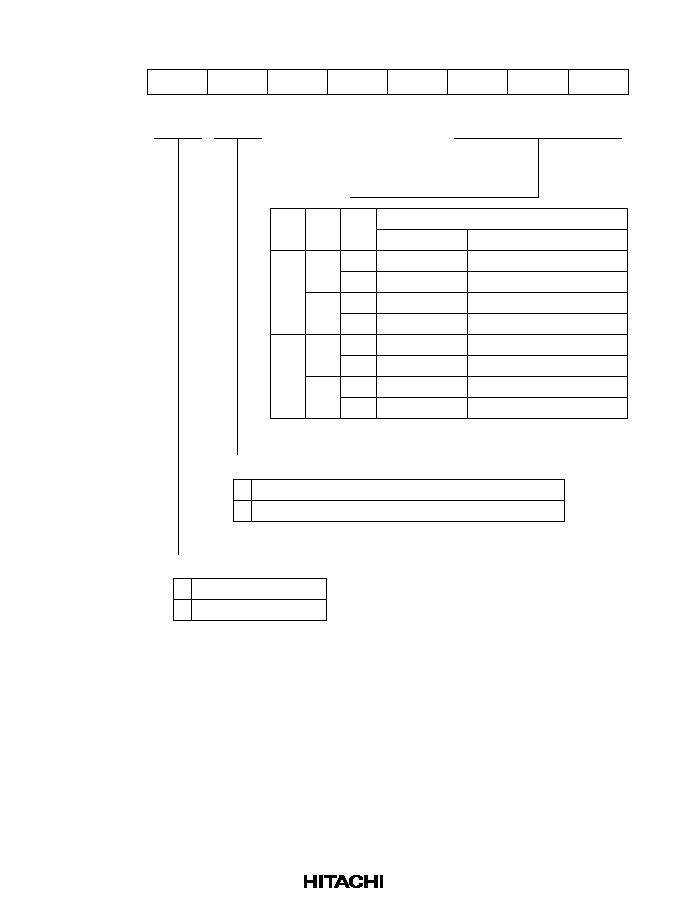
669
ICMR--I
2
C Bus Mode Register
H'DF
I
2
C
Bit
Initial value
Read/Write
7
MLS
0
R/W
6
WAIT
0
R/W
5
--
1
--
4
--
1
--
3
--
1
--
0
BC0
0
R/W
2
BC2
0
R/W
1
BC1
0
R/W
Bit Counter
BC0
Serial Mode
8
1
2
3
4
5
6
7
Wait Insertion Bit
0
1
Data and acknowledge transferred consecutively
Wait inserted between data and acknowledge
BC1
BC2
0
1
0
1
0
1
Bits/Frame
0
1
0
1
0
1
0
1
Acknowledgement Mode
9
2
3
4
5
6
7
8
MSB-First/LSB-First
0
1
MSB-first
LSB-first
670
ADDRA (H and L)--A/D Data Register A
H'E0, H'E1
A/D
Bit
Initial value
Read/Write
14
AD8
0
R
12
AD6
0
R
10
AD4
0
R
8
AD2
0
R
6
AD0
0
R
0
--
0
R
4
--
0
R
2
--
0
R
A/D Conversion Data
10-bit data giving an A/D conversion result
15
AD9
0
R
13
AD7
0
R
11
AD5
0
R
9
AD3
0
R
7
AD1
0
R
1
--
0
R
5
--
0
R
3
--
0
R
ADDRA H
ADDRA L
Reserved Bits
ADDRB (H and L)--A/D Data Register B
H'E2, H'E3
A/D
Bit
Initial value
Read/Write
14
AD8
0
R
12
AD6
0
R
10
AD4
0
R
8
AD2
0
R
6
AD0
0
R
0
--
0
R
4
--
0
R
2
--
0
R
A/D Conversion Data
10-bit data giving an A/D conversion result
15
AD9
0
R
13
AD7
0
R
11
AD5
0
R
9
AD3
0
R
7
AD1
0
R
1
--
0
R
5
--
0
R
3
--
0
R
ADDRB H
ADDRB L
Reserved Bits
671
ADDRC (H and L)--A/D Data Register C
H'E4, H'E5
A/D
Bit
Initial value
Read/Write
14
AD8
0
R
12
AD6
0
R
10
AD4
0
R
8
AD2
0
R
6
AD0
0
R
0
--
0
R
4
--
0
R
2
--
0
R
A/D Conversion Data
10-bit data giving an A/D conversion result
15
AD9
0
R
13
AD7
0
R
11
AD5
0
R
9
AD3
0
R
7
AD1
0
R
1
--
0
R
5
--
0
R
3
--
0
R
ADDRC H
ADDRC L
Reserved Bits
ADDRD (H and L)--A/D Data Register D
H'E6, H'E7
A/D
Bit
Initial value
Read/Write
14
AD8
0
R
12
AD6
0
R
10
AD4
0
R
8
AD2
0
R
6
AD0
0
R
0
--
0
R
4
--
0
R
2
--
0
R
A/D Conversion Data
10-bit data giving an A/D conversion result
15
AD9
0
R
13
AD7
0
R
11
AD5
0
R
9
AD3
0
R
7
AD1
0
R
1
--
0
R
5
--
0
R
3
--
0
R
ADDRD H
ADDRD L
Reserved Bits
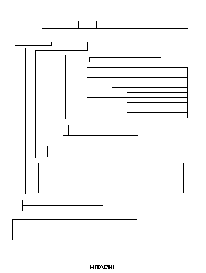
672
ADCSR--A/D Control/Status Register
H'E8
A/D
Bit
Initial value
Read/Write
7
ADF
0
R/(W)
6
ADIE
0
R/W
5
ADST
0
R/W
4
SCAN
0
R/W
3
CKS
0
R/W
0
CH0
0
R/W
2
CH2
0
R/W
1
CH1
0
R/W
Channel Select
Clock Select
0
1
Conversion time = 266 states (max)
Conversion time = 134 states (max)
*
Note:
*
Only 0 can be written, to clear the flag.
CH2
0
1
CH1
0
1
0
1
CH0
0
1
0
1
0
1
0
1
Single Mode
AN
0
AN
1
AN
2
AN
3
AN
4
AN
5
AN
6
AN
7
Scan Mode
AN
0
AN
0
, AN
1
AN
0
to AN
2
AN
0
to AN
3
AN
4
AN
4
, AN
5
AN
4
to AN
6
AN
4
to AN
7
Scan Mode
0
1
Single mode
Scan mode
A/D Start
0
1
A/D conversion is halted.
A/D Interrupt Enable
0
1
The A/D interrupt request (ADI) is disabled.
The A/D interrupt request (ADI) is enabled.
A/D End Flag
0
1
Cleared from 1 to 0 when CPU reads ADF = 1, then writes 0 in ADF.
Set to 1 at the following times:
∑ Single mode: at the completion of A/D conversion
∑ Scan mode: when all selected channels have been converted.
Single mode:
One A/D conversion is performed, then this bit is automatically cleared to 0.
Scan mode:
A/C conversion starts and continues cyclically on all selected channels until 0 is
written in this bit.
∑
∑
Note: ¯
P
= ¯
Group Selection Channel Selection
Description
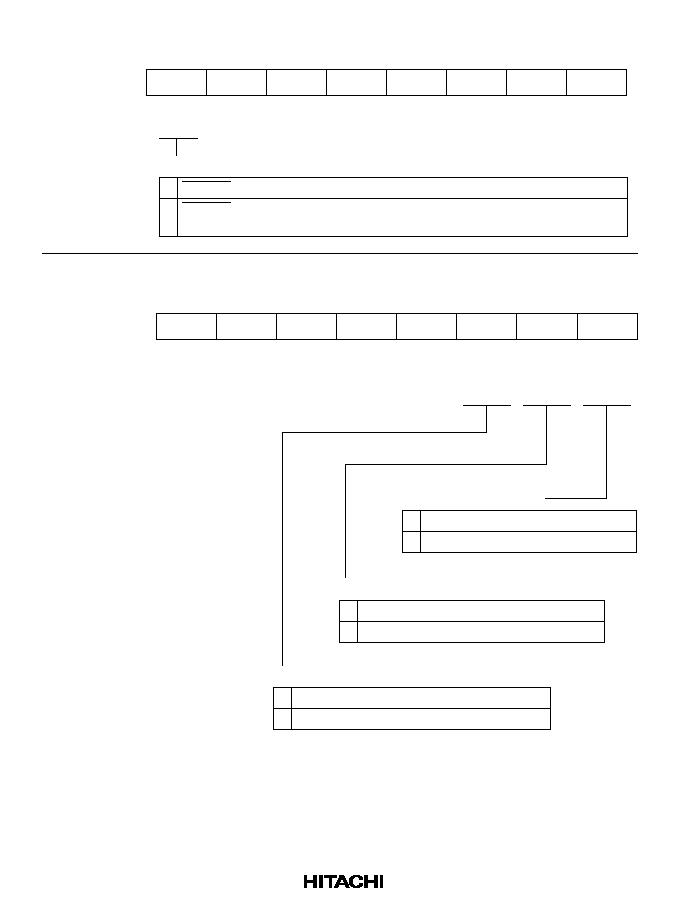
673
ADCR--A/D Control Register
H'E9
A/D
Trigger Enable
0
1
ADTRG is disabled.
ADTRG is enabled. A/D conversion can be started by external trigger,
or by software.
Bit
Initial value
Read/Write
7
TRGE
0
R/W
6
--
1
--
5
--
1
--
4
--
1
--
3
--
1
--
0
--
1
--
2
--
1
--
1
--
1
--
HICR--Host Interface Control Register
H'F0
HIF
Bit
Initial value
Host Read/Write
Slave Read/Write
7
--
1
--
--
6
--
1
--
--
5
--
1
--
--
4
--
1
--
--
3
--
1
--
--
0
FGA20E
0
--
R/W
2
IBFIE2
0
--
R/W
1
IBFIE1
0
--
R/W
Fast Gate A20 Enable
0
1
Fast A20 gate function disabled
Fast A20 gate function enabled
Input Buffer Full Interrupt Enable 1
0
1
IDR1 input buffer full interrupt disabled
IDR1 input buffer full interrupt enabled
Input Buffer Full Interrupt Enable 2
0
1
IDR2 input buffer full interrupt disabled
IDR2 input buffer full interrupt enabled

674
KMIMR--Keyboard Matrix Interrupt Mask Register
H'F1
System Control
Bit
Initial value
Read/Write
7
KMIMR7
1
R/W
6
KMIMR6
0
R/W
5
KMIMR5
1
R/W
4
KMIMR4
1
R/W
3
KMIMR3
1
R/W
0
KMIMR0
1
R/W
2
KMIMR2
1
R/W
1
KMIMR1
1
R/W
Keyboard Matrix Interrupt Mask
0
1
Key-sense input interrupt request enabled
Key-sense input interrupt request disabled (initial value)
*
Note:
*
Initial value of KMIMR6 is 0.
KMPCR--Port 6 Input Pull-Up Control Register
H'F2
Port 6
Bit
Initial value
Read/Write
7
KM
7
PCR
0
R/W
6
KM
6
PCR
0
R/W
5
KM
5
PCR
0
R/W
4
KM
4
PCR
0
R/W
3
KM
3
PCR
0
R/W
0
KM
0
PCR
0
R/W
2
KM
2
PCR
0
R/W
1
KM
1
PCR
0
R/W
Port 6 Input Pull-Up Control
0
1
Input pull-up transistor is off. (Initial value)
Input pull-up transistor is on.
IDR1--Input Data Register 1
H'F4
HIF
Bit
Initial value
Host Read/Write
Slave Read/Write
7
IDR7
--
W
R
6
IDR6
--
W
R
5
IDR5
--
W
R
4
IDR4
--
W
R
3
IDR3
--
W
R
0
IDR0
--
W
R
2
IDR2
--
W
R
1
IDR1
--
W
R
Input data (command or data input from host processor)

675
ODR1--Output Data Register 1
H'F5
HIF
Bit
Initial value
Host Read/Write
Slave Read/Write
7
ODR7
--
R
R/W
6
ODR6
--
R
R/W
5
ODR5
--
R
R/W
4
ODR4
--
R
R/W
3
ODR3
--
R
R/W
0
ODR0
--
R
R/W
2
ODR2
--
R
R/W
1
ODR1
--
R
R/W
Output data (data output to host processor)
STR1--Status Register 1
H'F6
HIF
Bit
Initial value
Host Read/Write
Slave Read/Write
7
DBU
0
R
R/W
6
DBU
0
R
R/W
5
DBU
0
R
R/W
4
DBU
0
R
R/W
3
C/D
0
R
R
0
OBF
0
R
R
2
DBU
0
R
R/W
1
IBF
0
R
R
Output Buffer Full
0
1
Host has read ODR1
Slave has written to ODR1
Input Buffer Full
0
1
Slave has read IDR1
Host has written to IDR1
Defined By User
Command/Data
0
1
IDR1 contains data
IDR1 contains a command
Defined By User

676
DADR0--D/A Data Register 0
H'F8
D/A
Bit
Initial value
Read/Write
7
0
R/W
6
0
R/W
5
0
R/W
4
0
R/W
3
0
R/W
0
0
R/W
2
0
R/W
1
0
R/W
Data to be converted
DADR1--D/A Data Register 1
H'F9
D/A
Bit
Initial value
Read/Write
7
0
R/W
6
0
R/W
5
0
R/W
4
0
R/W
3
0
R/W
0
0
R/W
2
0
R/W
1
0
R/W
Data to be converted
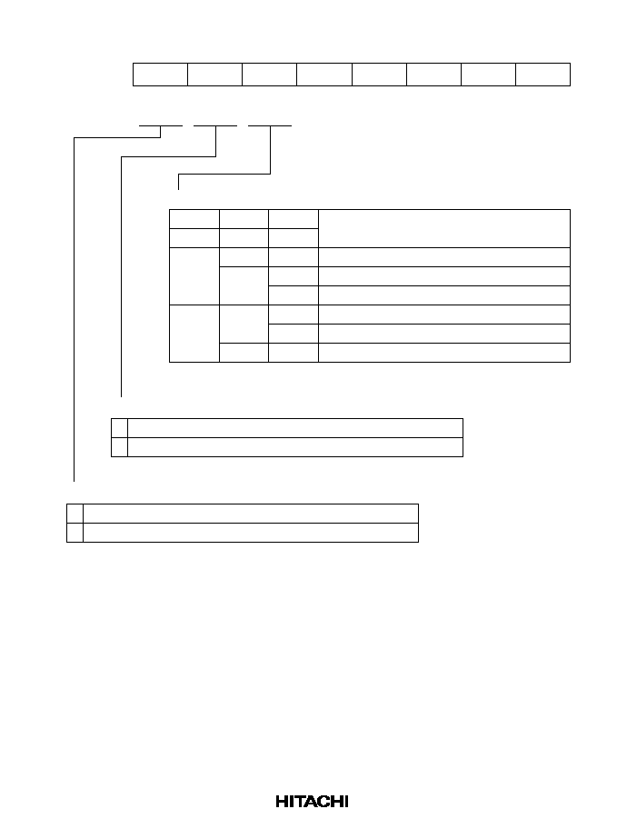
677
DACR--D/A Control Register
H'FA
D/A
Bit
Initial value
Read/Write
7
DAOE1
0
R/W
6
DAOE0
0
R/W
5
DAE
0
R/W
4
--
1
--
3
--
1
--
0
--
1
--
2
--
1
--
1
--
1
--
D/A Enable
DAOE1
D/A Output Enable 0
0
1
Analog output at DA0 disabled
Analog conversion in channel 0 and output at DA0 enabled
Description
0
1
DAOE0
DAE
Bit 7
Bit 6
Bit 5
Channels 0 and 1 disabled
Channel 0 enabled, channel 1 disabled
Channels 0 and 1 enabled
Channel 0 disabled, channel 1 enabled
Channels 0 and 1 enabled
Channels 0 and 1 enabled
0
1
0
1
--
0
1
0
1
--
D/A Output Enable 1
0
1
Analog output at DA1 disabled
Analog conversion in channel 1 and output at DA1 enabled
678
IDR2--Input Data Register 2
H'FC
HIF
Bit
Initial value
Host Read/Write
Slave Read/Write
7
IDR7
--
W
R
6
IDR6
--
W
R
5
IDR5
--
W
R
4
IDR4
--
W
R
3
IDR3
--
W
R
0
IDR0
--
W
R
2
IDR2
--
W
R
1
IDR1
--
W
R
Input data (command or data input from host processor)
ODR2--Output Data Register 2
H'FD
HIF
Bit
Initial value
Host Read/Write
Slave Read/Write
7
ODR7
--
R
R/W
6
ODR6
--
R
R/W
5
ODR5
--
R
R/W
4
ODR4
--
R
R/W
3
ODR3
--
R
R/W
0
ODR0
--
R
R/W
2
ODR2
--
R
R/W
1
ODR1
--
R
R/W
Output data (data output to host processor)
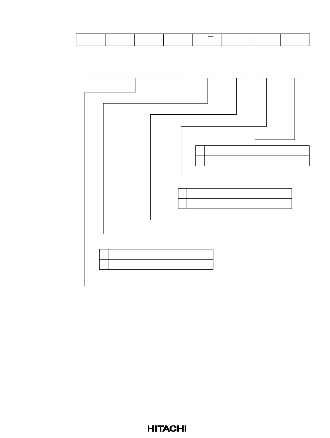
679
STR2--Status Register 2
H'FE
HIF
Bit
Initial value
Host Read/Write
Slave Read/Write
7
DBU
0
R
R/W
6
DBU
0
R
R/W
5
DBU
0
R
R/W
4
DBU
0
R
R/W
3
C/D
0
R
R
0
OBF
0
R
R
2
DBU
0
R
R/W
1
IBF
0
R
R
Output Buffer Full
0
1
Host has read ODR2
Slave has written to ODR2
Input Buffer Full
0
1
Slave has read IDR2
Host has written to IDR2
Defined By User
Command/Data
0
1
IDR2 contains data
IDR2 contains a command
Defined By User
680
Appendix C I/O Port Block Diagrams
Note:
"Reset" here means "reset + hardware standby."
C.1
Port 1 Block Diagram
WP1P:
WP1D:
WP1:
RP1P:
RP1:
n = 0 to 7
Note:
*
Set priority
Write to P1PCR
Write to P1DDR
Write to port 1
Read P1PCR
Read port 1
Reset
R
Q
D
C
P1
n
PCR
WP1P
Reset
Mode 1
R
S
Q
D
C
P1
n
DDR
P1
n
WP1D
Reset
R
Q
D
C
P1
n
DR
WP1
RP1
*
RP1P
Hardware standby
Mode 3
Mode 1 or 2
Internal data bus
Internal lower address bus
Figure C.1 Port 1 Block Diagram
681
C.2
Port 2 Block Diagram
WP2P:
WP2D:
WP2:
RP2P:
RP2:
n = 0 to 7
Note:
*
Set priority
Write to P2PCR
Write to P2DDR
Write to port 2
Read P2PCR
Read port 2
Reset
R
Q
D
C
P2
n
PCR
WP2P
Reset
Mode 1
R
S
Q
D
C
P2
n
DDR
P2
n
WP2D
Reset
R
Q
D
C
P2
n
DR
WP2
RP2
*
RP2P
Hardware standby
Mode 3
Mode 1 or 2
Internal data bus
Internal lower address bus
Figure C.2 Port 2 Block Diagram

682
C.3
Port 3 Block Diagram
WP3P:
WP3D:
WP3:
RP3P:
RP3:
n = 0 to 7
Write to P3PCR
Write to P3DDR
Write to port 3
Read P3PCR
Read port 3
Reset
Reset
R
Q
D
C
P3
n
PCR
WP3P
P3
n
External address
write
RP3P
Modes 1 or 2
R
Q
D
C
P3
n
DDR
WP3D
R
D
C
P3
n
DR
Reset
WP3
HIE Mode 3
Q
Internal data bus
Host interface data bus
External address
read
RP3
CS
IOW
CS
IOR
Figure C.3 Port 3 Block Diagram
683
C.4
Port 4 Block Diagrams
WP4D:
WP4:
RP4:
n = 0, 2
Write to P4DDR
Write to port 4
Read port 4
Reset
R
Q
D
C
P4
n
DDR
WP4D
Reset
R
Q
D
C
P4
n
DR
WP4
P4
n
RP4
8-bit timer
Counter clock input
Counter reset input
Internal data bus
Figure C.4 (a) Port 4 Block Diagram (Pins P4
0
, P4
2
)
684
WP4D:
WP4:
RP4:
n = 1, 6, 7
Reset
8-bit timer output
Write to P4DDR
Write to port 4
Read port 4
Output enable
8-bit timer, PWM timer
R
Q
D
C
P4nDR
WP4
Reset
R
Q
D
C
P4
n
DDR
WP4D
P4
n
RP4
Internal data bus
PWM timer output
Figure C.4 (b) Port 4 Block Diagram (Pins P4
1
, P4
6
, P4
7
)
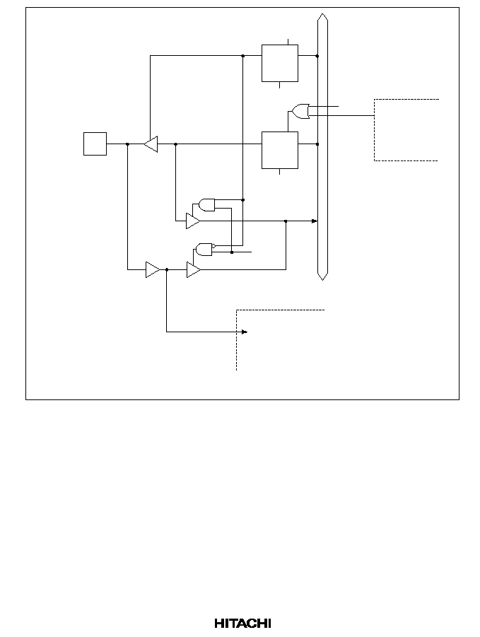
685
WP4D:
WP4:
RP4:
n = 3, 5
Write to P4DDR
Write to port 4
*
Read port 4
Reset
R
Q
D
C
P4
n
DDR
WP4D
R
Q
D
C
P4
n
DR
WP4
P4
n
RP4
8-bit timer
Counter clock input
Counter reset input
Internal data bus
Reset
RESOBF2,
RESOBF1
(reset HIRQ
11
and HIRQ
12
,
respectively)
HIF
Note:
*
Refer to table 14-9, Host Interrupt Set/Clear Conditions.
Figure C.4 (c) Port 4 Block Diagram (Pins P4
3
, P4
5
)
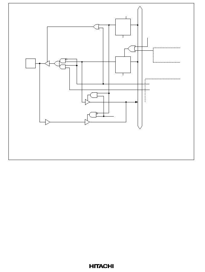
686
WP4D:
WP4:
RP4:
Write to P4DDR
Write to port 4
*
Read port 4
Output enable
8-bit timer output
8-bit timer
R
Q
D
C
P4
4
DR
WP4
Reset
R
Q
D
C
P4
4
DDR
WP4D
P4
n
RP4
Internal data bus
Reset
HIF
RESOBF1
(reset HIRQ
1
)
Note:
*
Refer to table 14-9, Host Interrupt Set/Clear Conditions.
Figure C.4 (d) Port 4 Block Diagram (Pin P4
4
)

687
C.5
Port 5 Block Diagrams
WP5D:
WP5:
RP5:
Reset
Serial transmit data
Write to P5DDR
Write to port 5
Read port 5
Output enable
SCI
R
Q
D
C
P5
0
DR
WP5
Reset
R
Q
D
C
P5
0
DDR
WP5D
P5
0
RP5
Internal data bus
Figure C.5 (a) Port 5 Block Diagram (Pin P5
0
)
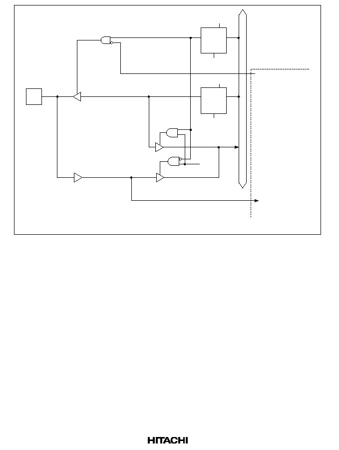
688
WP5D:
WP5:
RP5:
Reset
Serial receive data
Write to P5DDR
Write to port 5
Read port 5
Input enable
SCI
R
Q
D
C
P5
1
DR
WP5
Reset
R
Q
D
C
P5
1
DDR
WP5D
P5
1
RP5
Internal data bus
Figure C.5 (b) Port 5 Block Diagram (Pin P5
1
)

689
WP5D:
WP5:
RP5:
Reset
Clock output
Write to P5DDR
Write to port 5
Read port 5
Clock output enable
SCI
R
Q
D
C
P5
2
DR
WP5
Reset
R
Q
D
C
P5
2
DDR
WP5D
P5
2
RP5
Clock input
Clock input enable
Internal data bus
Figure C.5 (c) Port 5 Block Diagram (Pin P5
2
)

690
C.6
Port 6 Block Diagrams
WP6D:
WP6:
RP6:
RP6P:
WP6P:
n = 0, 2, 3, 4, 5
Write to P6DDR
Write to port 6
Read port 6
Read KMPCR
Write to KMPCR
Reset
R
Q
D
C
P6
n
DDR
WP6D
Reset
R
Q
D
C
P6
n
DR
WP6
P6
n
RP6
Free-running timer
Input capture input
Counter clock input
Internal data bus
Reset
WP6P
RP6P
Hardware standby
R
Q
D
C
KM
n
PCR
Key-sense interrupt input
KMIMR
n
Figure C.6 (a) Port 6 Block Diagram (Pins P6
0
, P6
2
, P6
3
, P6
4
, P6
5
)
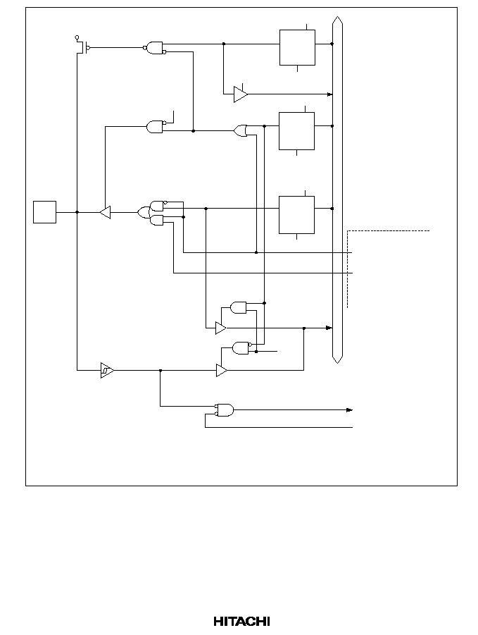
691
WP6D:
WP6:
RP6:
RP6P:
WP6P:
Reset
Output compare output
Write to P6DDR
Write to port 6
Read port 6
Read KMPCR
Write to KMPCR
Output enable
Free-running timer
R
Q
D
C
P6
1
DR
WP6
Reset
R
Q
D
C
P6
1
DDR
WP6D
P6
1
RP6
Internal data bus
Key-sense interrupt input
KMIMR
1
Reset
WP6P
RP6P
Hardware standby
R
Q
D
C
KM
1
PCR
Figure C.6 (b) Port 6 Block Diagram (Pin P6
1
)
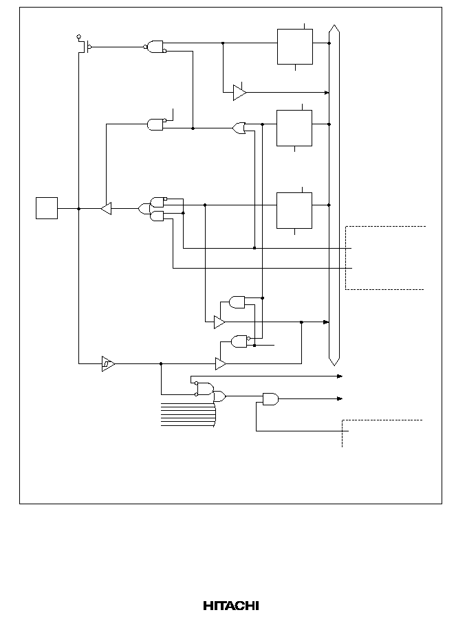
692
Reset
WP6P
RP6P
Hardware standby
R
Q
D
C
KM
6
PCR
WP6D:
WP6:
RP6:
RP6P:
WP6P:
Reset
Output compare
output
Write to P6DDR
Write to port 6
Read port 6
Read KMPCR
Write to KMPCR
Output enable
Free-running timer
IRQ enable register
R
Q
D
C
P6
6
DR
WP6
Reset
R
Q
D
C
P6
6
DDR
WP6D
P6
6
RP6
IRQ6 enable
IRQ
6
input
Internal data bus
KMIMR
6
Other key-sense
interrupt inputs
Figure C.6 (c) Port 6 Block Diagram (Pin P6
6
)
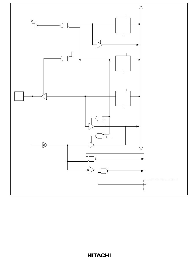
693
Reset
WP6P
RP6P
Hardware standby
R
Q
D
C
KM
7
PCR
Reset
R
Q
D
C
P6
7
DDR
WP6D
Reset
R
Q
D
C
P6
7
DR
WP6
P6
7
RP6
WP6D:
WP6:
RP6:
RP6P:
WP6P:
Write to P6DDR
Write to port 6
Read port 6
Read KMPCR
Write to KMPCR
IRQ enable register
IRQ7 enable
IRQ
7
input
Internal data bus
KMIMR
7
Key-sense interrupt input
Figure C.6 (d) Port 6 Block Diagram (Pin P6
7
)

694
C.7Port 7
Block Diagrams
P7
n
RP7:
n = 0 to 5
Read port 7
A/D converter
Analog input
Internal data bus
RP7
Figure C.7 (a) Port 7 Block Diagram (Pins P7
0
to P7
5
)
P7
n
RP7:
n = 6, 7
Read port 7
A/D converter
D/A converter
Analog input
Output enable
Internal data bus
RP7
Analog output
Figure C.7 (b) Port 7 Block Diagram (Pins P7
6
and P7
7
)
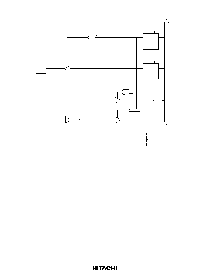
695
C.8
Port 8 Block Diagrams
WP8D:
WP8:
RP8:
Write to P8DDR
Write to port 8
Read port 8
Reset
R
Q
D
C
P8
0
DDR
WP8D
Reset
R
Q
D
C
P8
0
DR
WP8
P8
0
RP8
Internal data bus
HIF
HA
0
HIE
Figure C.8 (a) Port 8 Block Diagram (Pin P8
0
)
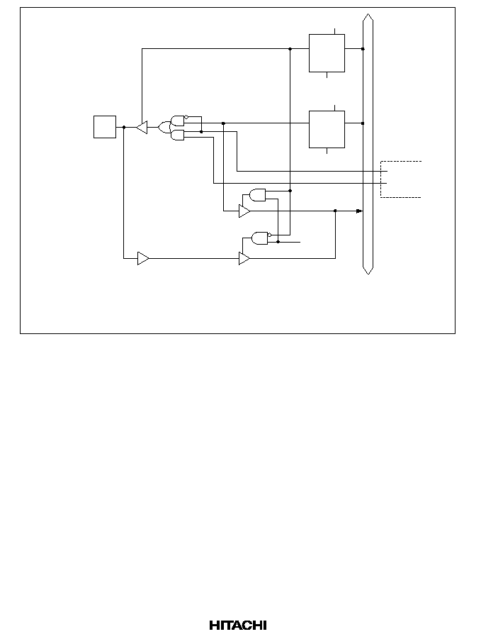
696
WP8D:
WP8:
RP8:
Reset
FGA
20
Write to P8DDR
Write to port 8
Read port 8
FGA
20
E
HIF
R
Q
D
C
P8
1
DR
WP8
Reset
R
Q
D
C
P8
1
DDR
WP8D
P8
1
RP8
Internal data bus
Figure C.8 (b) Port 8 Block Diagram (Pin P8
1
)
697
WP8D:
WP8:
RP8:
n = 2, 3
Reset
Write to P8DDR
Write to port 8
Read port 8
R
Q
D
C
P8
n
DR
WP8
Reset
R
Q
D
C
P8
n
DDR
WP8D
P8
n
RP8
HIE
HIF
Input (
CS
1
,
IOR
)
Internal data bus
Figure C.8 (c) Port 8 Block Diagram (Pins P8
2
, P8
3
)
698
WP8D:
WP8:
RP8:
Reset
Write to P8DDR
Write to port 8
Read port 8
R
Q
D
C
P8
4
DR
WP8
Reset
R
Q
D
C
P8
4
DDR
WP8D
P8
4
RP8
Internal data bus
IRQ enable register
IRQ3 enable
HIF
IOW
IRQ
3
input
HIE STAC
SCI
Output enable
Serial transmit data
Figure C.8 (d) Port 8 Block Diagram (Pin P8
4
)

699
P8
5
Reset
WP8D:
WP8:
RP8:
Write to P9DDR
Write to port 8
Read port 8
R
Q
D
C
P8
5
DDR
WP8D
Reset
R
Q
D
C
P8
5
DR
WP8
RP8
HIF
HIE
STAC
CS
2
input
IRQ
4
input
IRQ enable register
IRQ4 enable
Internal data bus
SCI
Input enable
Serial receive data
Figure C.8 (e) Port 8 Block Diagram (Pin P8
5
)
700
Reset
WP8
Reset
R
Q
D
C
P8
6
DDR
WP8D
P8
6
RP8
Internal data bus
IRQ enable register
IRQ5 enable
IRQ
5
input
SCI
Clock output enable
Clock output
Clock input enable
Clock input
R
Q
D
C
P8
6
DR
WP8D:
WP8:
RP8:
Write to P8DDR
Write to port 8
Read port 8
Note: For a block diagram when the SCL pin function is selected, see section 13,
I
2
C Bus Interface.
Figure C.8 (f) Port 8 Block Diagram (Pin P8
6
)
701
C.9
Port 9 Block Diagrams
P9
0
Reset
WP9D:
WP9:
RP9:
Write to P9DDR
Write to port 9
Read port 9
R
Q
D
C
P9
0
DDR
WP9D
Reset
R
Q
D
C
P9
0
DR
WP9
RP9
IRQ
2
input
IRQ2 enable
IRQ enable register
External trigger
input
A/D converter
ECS
2
input
HIE
STAC
HIF
Internal data bus
Figure C.9 (a) Port 9 Block Diagram (Pin P9
0
)
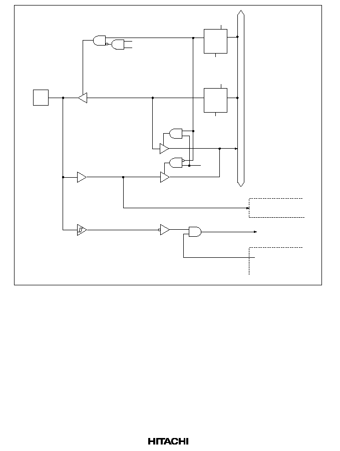
702
P9
1
Reset
Internal data bus
WP9D:
WP9:
RP9:
Write to P9DDR
Write to port 9
Read port 9
R
Q
D
C
P9
1
DDR
WP9D
Reset
R
Q
D
C
P9
1
DR
WP9
RP9
IRQ1 enable
IRQ enable register
IRQ
1
input
HIE
STAC
HIF
EIOW
input
Figure C.9 (b) Port 9 Block Diagram (Pin P9
1
)
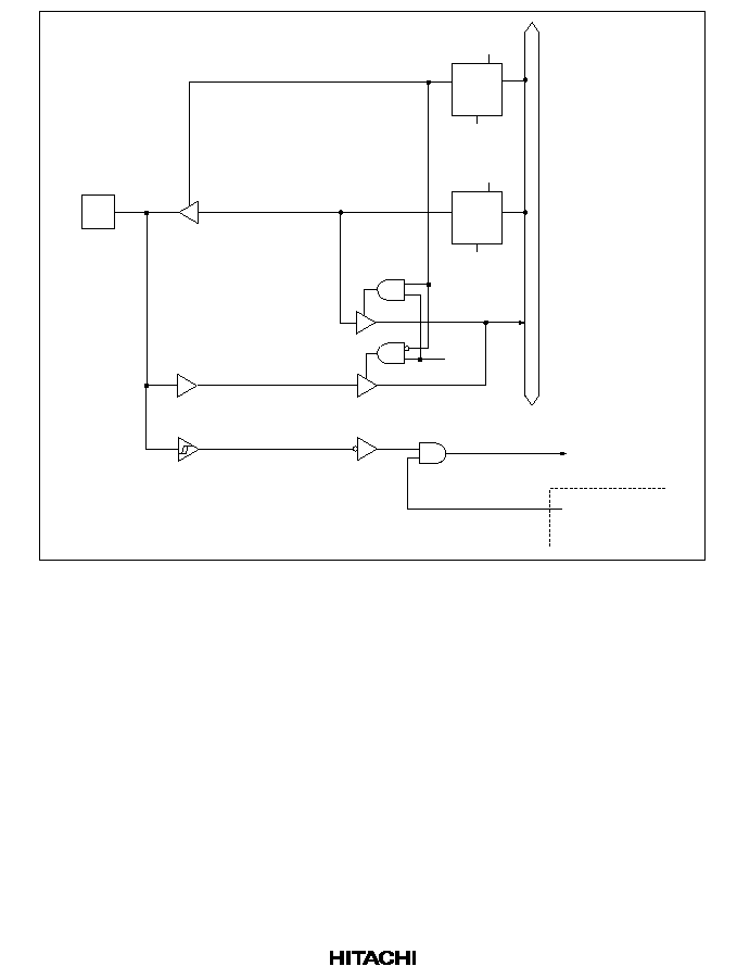
703
P9
2
Reset
Internal data bus
WP9D:
WP9:
RP9:
Write to P9DDR
Write to port 9
Read port 9
R
Q
D
C
P9
2
DDR
WP9D
Reset
R
Q
D
C
P9
2
DR
WP9
RP9
IRQ0 enable
IRQ enable register
IRQ
0
input
Figure C.9 (c) Port 9 Block Diagram (Pin P9
2
)

704
P9
n
Reset
Internal data bus
WP9D:
WP9:
RP9:
n = 3, 4, 5
Write to P9DDR
Write to port 9
Read port 9
R
Q
D
C
P9
n
DDR
WP9D
Reset
R
Q
D
C
P9
n
DR
WP9
RP9
Hardware standby
Mode 1 or 2
Mode 3
RD output
WR output
AS output
Mode 1 or 2
Figure C.9 (d) Port 9 Block Diagram (Pins P9
3
, P9
4
, P9
5
)
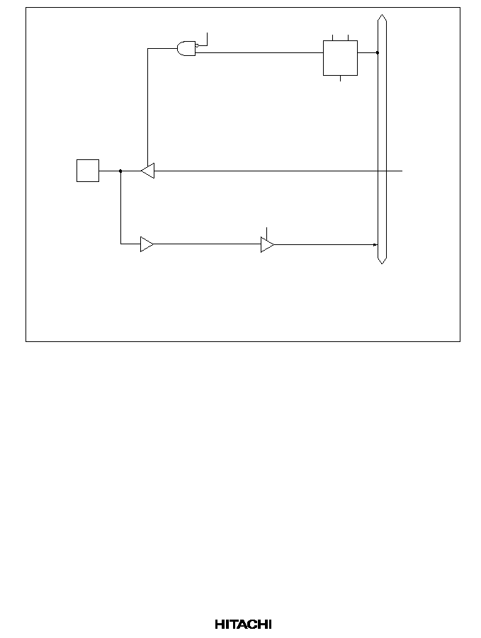
705
P9
6
Reset
WP9D:
WP9:
RP9:
Note:
*
Set priority
Write to P9DDR
Write to port 9
Read port 9
R
S
Q
D
C
P9
6
DDR
WP9D
RP9
¯
Hardware standby
Mode 1 or 2
*
Internal data bus
Figure C.9 (e) Port 9 Block Diagram (Pin P9
6
)
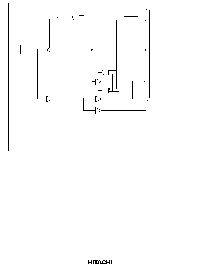
706
P9
7
Mode 1 or 2
Reset
WP9D:
WP9:
RP9:
Write to P9DDR
Write to port 9
Read port 9
R
Q
D
C
P9
7
DDR
WP9D
Reset
R
Q
D
C
P9
7
DR
WP9
RP9
WAIT input
Note: For a block diagram when the SDA pin function is selected, see section 13, I
2
C Bus Interface.
Internal data bus
Wait input enable
Figure C.9 (f) Port 9 Block Diagram (Pin P9
7
)

707
Appendix D Port States in Each Processing State
Table D.1
Port States
Port Name
(Multiplexed
Pin Names)
Mode
Reset
Hardware
Standby
Mode
Software
Standby Mode Sleep Mode
Program
Execution
State (Normal
Operation)
P1
7
to P1
0
1
L
T
L
keep
*
1
A
7
to A
0
A
7
to A
0
2
T
(DDR = 1)
L
(DDR = 0)
keep
Address/
input port
3
keep
I/O port
P2
7
to P2
0
1
L
T
L
keep
*
1
A
15
to A
8
A
15
to A
8
2
T
(DDR = 1)
L
(DDR = 0)
keep
Address/
input port
3
keep
I/O port
P3
7
to P3
0
1
T
T
T
T
D
7
to D
0
D
7
to D
0
2
3
keep
keep
I/O port
P4
7
to P4
0
1
T
T
keep
*
2
keep
I/O port
2
3
P5
2
to P5
0
1
T
T
keep
*
2
keep
I/O port
2
3
P6
7
to P6
0
1
T
T
keep
*
2
keep
I/O port
2
3
P7
7
to P7
0
1
T
T
T
T
Input port
2
3

708
Port Name
(Multiplexed
Pin Names)
Mode
Reset
Hardware
Standby
Mode
Software
Standby Mode Sleep Mode
Program
Execution
State (Normal
Operation)
P8
6
to P8
0
1
T
T
keep
*
2
keep
I/O port
2
3
P9
7
/
WAIT
1
T
T
T/keep
*
2
T/keep
WAIT
/
2
I/O port
3
keep
*
2
keep
I/O port
P9
6
/¯
1
Clock
T
H
Clock
Clock
2
output
output
output
3
T
(DDR = 1)
H
(DDR = 0)
T
(DDR = 1)
Clock output
(DDR = 0)
T
(DDR = 1)
Clock output
(DDR = 0)
Input port
P9
5
to P9
3
,
1
H
T
H
H
AS
,
WR
,
RD
AS
,
WR
,
RD
2
3
T
keep
keep
I/O port
P9
2
to P9
0
1
T
T
keep
keep
I/O port
2
3
Legend:
H:
High level
L:
Low level
T:
High impedance
keep: Input port becomes high-impedance (when DDR = 0 and PCR = 1, MOS input pull-ups
remain on), output port retains state
Notes:
*
1 With address outputs, the last address accessed is retained.
*
2 As on-chip supporting modules are initialized, becomes an I/O port determined by DDR
and DR.
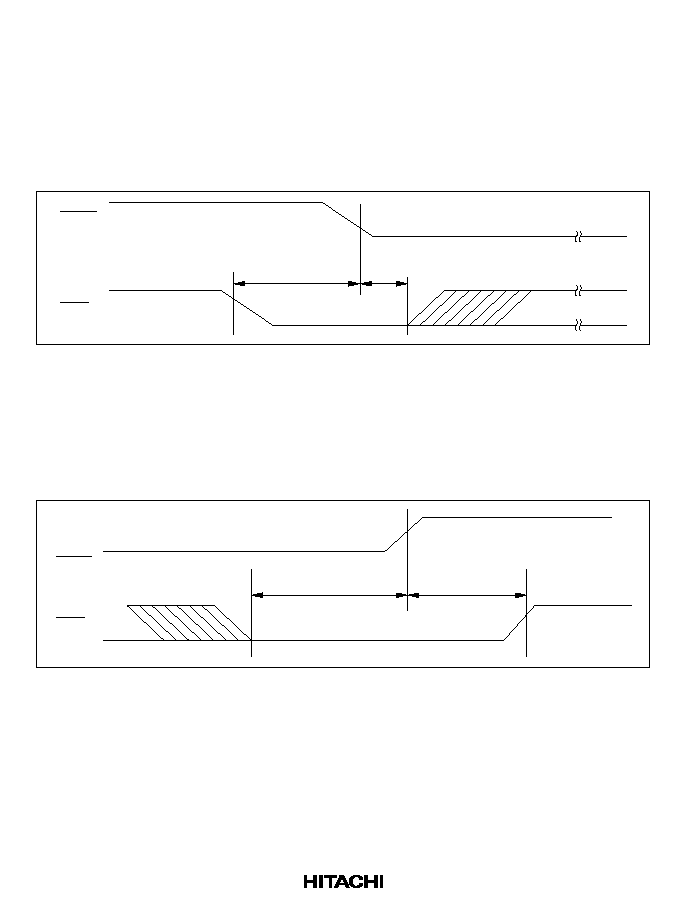
709
Appendix E Timing of Transition to and Recovery from
Hardware Standby Mode
Timing of Transition to Hardware Standby Mode
(1) To retain RAM contents when the RAME bit in SYSCR is set to 1, drive the
RES
signal low
10 system clock cycles before the
STBY
signal goes low, as shown below.
RES
must remain
low until
STBY
goes low (minimum delay from
STBY
low to
RES
high: 0 ns).
STBY
RES
t
1
10 t
cyc
t
2
0 ns
(2) When the RAME bit in SYSCR is cleared to 0 or when it is not necessary to retain RAM
contents,
RES
does not have to be driven low as in (1).
Timing of Recovery From Hardware Standby Mode: Drive the
RES
signal low approximately
100 ns before
STBY
goes high.
STBY
RES
t
100 ns
t
OSC

710
Appendix F Option List
Please check off the appropriate applications and enter the necessary information.
Date of order
Customer
Department
Name
ROM code name
LSI number
(Hitachi entry)
1. ROM Size
HD6433334Y
32 kbytes
HD6433394
32 kbytes
HD6433336Y
48 kbytes
HD6433396
48 kbytes
HD6433337Y
60 kbytes
HD64333397
60 kbytes
2. System Oscillator
Crystal oscillator
f = MHz
External clock
f = MHz
3. Power Supply Voltage/Maximum Operating Frequency
V
CC
= 4.5 V to 5.5 V (16 MHz max.)
V
CC
= 4.0 V to 5.5 V (12 MHz max.)
V
CC
= 2.7 V to 5.5 V (10 MHz max.)
Notes: 1. Please select the power supply voltage/operating frequency version according to the
power supply voltage to be used.
Example: For use at V
CC
= 4.5 V to 5.5 V/f = 10 MHz, select V
CC
= 4.5 V to 5.5 V
(16 MHz max.).
2. Please enter the power supply voltage and maximum operating frequency of the
selected version in accordance with the "Single-Chip Microcomputer Order
Specification".
711
ROM code name
LSI number
(Hitachi entry)
4. I
2
C Bus Option [H8/3337 Series]
I
2
C bus used
I
2
C bus not used
Notes: 1. "I
2
C bus used" includes all cases where data transfer is performed by means of the SCL
and SDA pins using the on-chip I
2
C bus interface function (hardware module). As long
as the I
2
C bus interface function (hardware module) is used, various bus interfaces with
different bus specifications and names are also included in "I
2
C bus used".
2. If "I
2
C bus not used" is selected, values cannot be set in I
2
C bus interface related
registers (ICCR, ICSR, ICDR, and ICMR). These registers return H'FF if read.
In the case of an emulator and the ZTAT and F-ZTAT versions, the "I
2
C bus used"
option is taken as being selected. If the "I
2
C bus not used" option is selected, care must
be taken to confirm that I
2
C bus interface related registers are not accessed.
For (1) Basic Items and the Microcomputer Family item in the "Single-Chip Microcomputer
Ordering Specifications Sheet", enter an item selected from the table below in accordance with the
combination of (1) and (4) above. When the "I
2
C bus used" option is selected, this should be
indicated again in (1) Basic Items, Special Specifications (Product Specifications, Marking
Specifications).
I
2
C
ROM Size
I
2
C bus used
I
2
C bus not used
32 kbytes
HD6433334W
HD6433334Y
48 kbytes
HD6433336W
HD6433336Y
60 kbytes
HD6433337W
HD6433337Y

712
Appendix G Product Code Lineup
Table G.1
H8/3397 Series, H8/3337 Series, H8/3334YF-ZTAT, and H8/3337YF-ZTAT
Product Code Lineup
Product Type
Product Code
Mark Code
Package (Hitachi
Package Code)
H8/3397
Mask ROM
Standard
HD6433397F
HD6433397(
***
)F
80-pin QFP (FP-80A)
version
products
HD6433397TF
HD6433397(
***
)TF
80-pin TQFP (TFP-80C)
HD6433397CP
HD6433397(
***
)CP
84-pin PLCC (CP-84)
H8/3396
Mask ROM
Standard
HD6433396F
HD6433396(
***
)F
80-pin QFP (FP-80A)
version
products
HD6433396TF
HD6433396(
***
)TF
80-pin TQFP (TFP80-C)
HD6433396CP
HD6433396(
***
)CP
84-pin PLCC (CP-84)
H8/3394
Mask ROM
Standard
HD6433394F
HD6433394(
***
)F
80-pin QFP (FP-80A)
version
products
HD6433394TF
HD6433394(
***
)TF
80-pin TQFP (TFP80-C)
HD6433394CP
HD6433394(
***
)CP
84-pin PLCC (CP-84)
H8/3337Y Flash
Dual-power-
HD64F3337YF16
HD64F3337YF16
80-pin QFP (FP-80A)
memory
supply F-ZTAT
HD64F3337YFLH16
HD64F3337YF16
version
version
HD64F3337YTF16
HD64F3337YTF16
80-pin TQFP (TFP-80C)
HD64F3337YTFLH16 HD64F3337YTF16
HD63F3337YCP16
HD64F3337YCP16
84-pin PLCC (CP-84)
Single-power-
HD64F3337SF16
HD64F3337F16
80-pin QFP (FP-80A)
supply F-ZTAT
version
HD64F3337STF16
HD64F3337TF16
80-pin TQFP (TFP-80C)
PROM
ZTAT
HD6473337YF16
HD6473337YF16
80-pin QFP (FP-80A)
version
version
HD6473337YTF16
HD6473337YTF16
80-pin TQFP (TFP-80C)
HD6473337YCP16
HD6473337YCP16
84-pin PLCC (CP-84)
Mask ROM
Standard
HD6433337YF
HD6433337Y(
***
)F
80-pin QFP (FP-80A)
version
products
HD6433337YTF
HD6433337Y(
***
)TF
80-pin TQFP (TFP-80C)
HD6433337YCP
HD6433337Y(
***
)CP 84-pin PLCC (CP-84)
Mask ROM
With I
2
C
HD6433337WF
HD6433337W(
***
)F
80-pin QFP (FP-80A)
version
interface
HD6433337WTF
HD6433337W(
***
)TF 80-pin TQFP (TFP-80C)
HD6433337WCP
HD6433337W(
***
)CP 84-pin PLCC (CP-84)

713
Product Type
Product Code
Mark Code
Package (Hitachi
Package Code)
H8/3336Y Mask ROM
Standard
HD6433336YF
HD6433336Y(
***
)F
80-pin QFP (FP-80A)
version
products
HD6433336YTF
HD6433336Y(
***
)TF
84-pin TQFP (TFP-80C)
HD6433336YCP
HD6433336Y(
***
)CP 84-pin PLCC (CP-84)
With I
2
C bus
HD6433336WF
HD6433336W(
***
)F
80-pin QFP (FP-80A)
interface
HD6433336WTF
HD6433336W(
***
)TF 80-pin TQFP (FP-80C)
HD6433336WCP
HD6433336W(
***
)CP 80-pin LCC (CP-84)
H8/3334Y Flash
F-ZTAT
HD64F3334YF16
HD64F3334YF16
80-pin QFP (FP-80A)
memory
version
HD64F3334YFLH16
HD64F3334YF16
version
HD64F3334YTF16
HD64F3334YTF16
80-pin TQFP (TFP-80C)
HD64F3334YTFLH16 HD64F3334YTF16
HD64F3334YCP16
HD64F3334YCP16
84-pin PLCC (CP-84)
PROM
ZTAT
HD6473334YF16
HD6473334YF16
80-pin QFP (FP-80A)
version
version
HD6473334YTF16
HD6473334YTF16
80-pin TQFP (TFP-80C)
HD6473334YCP16
HD6473334YCP16
84-pin PLCC (CP-84)
Mask ROM
Standard
HD6433334YF
HD6433334Y(
***
)F
80-pin QFP (FP-80A)
version
products
HD6433334YTF
HD6433334Y(
***
)TF
80-pin TQFP (TFP-80C)
With I
2
C bus
HD6433334YCP
HD6433334Y(
***
)CP 84-pin PLCC (CP-84)
interface
HD6433334WF
HD6433334W(
***
)F
80-pin QFP (FP-80A)
HD6433334WTF
HD6433334W(
***
)TF 80-pin TQFP (TFP-80C)
HD6433334WCP
HD6433334W(
***
)CP 84-pin PLCC (CP-84)
Note:
(
***
) in the mark code for mask ROM versions is the ROM code.
The I
2
C bus interface is an option. Please note the following points when using this optional
function.
1. Notify your Hitachi sales representative that you will be using an optional function.
2. With mask ROM versions, optional functions can be used if the product code includes the
letter W in place of the letter Y (e.g. HD6433337WF, HD6433337WTF).
3. The product code is the same for ZTAT versions, but please be sure to notify Hitachi if you are
going to use this optional function.

714
Appendix H Package Dimensions
Figure H.1 shows the dimensions of the FP-80A package. Figure H.2 shows the dimensions of the
TFP-80C package. Figure H.3 shows the dimensions of the CP-84 package.
Hitachi Code
JEDEC
JEITA
Mass (reference value)
FP-80A
--
Conforms
1.2 g
*Dimension including the plating thickness
Base material dimension
60
0
∞
-
8
∞
0.10
0.12 M
17.2
±
0.3
41
61
80
1
20
40
21
17.2
±
0.3
*0.32
±
0.08
0.65
3.05 Max
1.6
0.8
±
0.3
14
2.70
*0.17
±
0.05
0.10
+
0.15
-
0.10
0.83
0.30
±
0.06
0.15
±
0.04
Unit: mm
Figure H.1 Package Dimensions (FP-80A)
715
Hitachi Code
JEDEC
JEITA
Mass (reference value)
TFP-80C
--
Conforms
0.4 g
*Dimension including the plating thickness
Base material dimension
0.10
M
0.10
0.5
±
0.1
0
∞
-
8
∞
1.20 Max
14.0
±
0.2
0.5
12
14.0
±
0.2
60
41
1
20
80
61
21
40
*0.17
±
0.05
1.0
*0.22
±
0.05
0.10
±
0.10
1.00
1.25
0.20
±
0.04
0.15
±
0.04
Unit: mm
Figure H.2 Package Dimensions (TFP-80C)
716
1.27
*0.42
±
0.10
29.28
28.20
±
0.50
28.20
±
0.50
4.40
±
0.20
2.55
±
0.15
0.10
53
33
54
74
75
84
1
11
12
32
0.75
30.23
+
0.12
-
0.13
30.23
+
0.12
-
0.13
1.94
0.90
0.38
±
0.08
0.20
M
Hitachi Code
JEDEC
JEITA
Mass (reference value)
CP-84
Conforms
Conforms
6.4 g
*Dimension including the plating thickness
Base material dimension
Unit: mm
Figure H.3 Package Dimensions (CP-84)

H8/3397 Series and H8/3337 Series
Hardware Manual
Publication Date: 1st Edition, September 1994
6th Edition, March 2002
Published by:
Business Planning Division
Semiconductor & Integrated Circuits
Hitachi, Ltd.
Edited by:
Technical Documentation Group
Hitachi Kodaira Semiconductor
Copyright © Hitachi, Ltd., 1994. All rights reserved. Printed in Japan.