H8/3069 F-ZTAT Hardware Manual

Regarding the change of names mentioned in the document, such as Hitachi
Electric and Hitachi XX, to Renesas Technology Corp.
The semiconductor operations of Mitsubishi Electric and Hitachi were transferred to Renesas
Technology Corporation on April 1st 2003. These operations include microcomputer, logic, analog
and discrete devices, and memory chips other than DRAMs (flash memory, SRAMs etc.)
Accordingly, although Hitachi, Hitachi, Ltd., Hitachi Semiconductors, and other Hitachi brand
names are mentioned in the document, these names have in fact all been changed to Renesas
Technology Corp. Thank you for your understanding. Except for our corporate trademark, logo and
corporate statement, no changes whatsoever have been made to the contents of the document, and
these changes do not constitute any alteration to the contents of the document itself.
Renesas Technology Home Page: http://www.renesas.com
Renesas Technology Corp.
Customer Support Dept.
April 1, 2003
To all our customers

Cautions
Keep safety first in your circuit designs!
1. Renesas Technology Corporation puts the maximum effort into making semiconductor products better
and more reliable, but there is always the possibility that trouble may occur with them. Trouble with
semiconductors may lead to personal injury, fire or property damage.
Remember to give due consideration to safety when making your circuit designs, with appropriate
measures such as (i) placement of substitutive, auxiliary circuits, (ii) use of nonflammable material or
(iii) prevention against any malfunction or mishap.
Notes regarding these materials
1. These materials are intended as a reference to assist our customers in the selection of the Renesas
Technology Corporation product best suited to the customer's application; they do not convey any
license under any intellectual property rights, or any other rights, belonging to Renesas Technology
Corporation or a third party.
2. Renesas Technology Corporation assumes no responsibility for any damage, or infringement of any
third-party's rights, originating in the use of any product data, diagrams, charts, programs, algorithms, or
circuit application examples contained in these materials.
3. All information contained in these materials, including product data, diagrams, charts, programs and
algorithms represents information on products at the time of publication of these materials, and are
subject to change by Renesas Technology Corporation without notice due to product improvements or
other reasons. It is therefore recommended that customers contact Renesas Technology Corporation
or an authorized Renesas Technology Corporation product distributor for the latest product information
before purchasing a product listed herein.
The information described here may contain technical inaccuracies or typographical errors.
Renesas Technology Corporation assumes no responsibility for any damage, liability, or other loss
rising from these inaccuracies or errors.
Please also pay attention to information published by Renesas Technology Corporation by various
means, including the Renesas Technology Corporation Semiconductor home page
(http://www.renesas.com).
4. When using any or all of the information contained in these materials, including product data, diagrams,
charts, programs, and algorithms, please be sure to evaluate all information as a total system before
making a final decision on the applicability of the information and products. Renesas Technology
Corporation assumes no responsibility for any damage, liability or other loss resulting from the
information contained herein.
5. Renesas Technology Corporation semiconductors are not designed or manufactured for use in a device
or system that is used under circumstances in which human life is potentially at stake. Please contact
Renesas Technology Corporation or an authorized Renesas Technology Corporation product distributor
when considering the use of a product contained herein for any specific purposes, such as apparatus or
systems for transportation, vehicular, medical, aerospace, nuclear, or undersea repeater use.
6. The prior written approval of Renesas Technology Corporation is necessary to reprint or reproduce in
whole or in part these materials.
7. If these products or technologies are subject to the Japanese export control restrictions, they must be
exported under a license from the Japanese government and cannot be imported into a country other
than the approved destination.
Any diversion or reexport contrary to the export control laws and regulations of Japan and/or the
country of destination is prohibited.
8. Please contact Renesas Technology Corporation for further details on these materials or the products
contained therein.

H8/3069 F-ZTATTM
HD64F3069
Hardware Manual
ADE-602-263A
Rev. 2.0
12/10/02
Hitachi, Ltd.
The revision list can be viewed directly by
clicking the title page.
The rivision list summarizes the locations of
revisions and additions. Details should always be
checked by referring to the relevant text.

Cautions
1. Hitachi neither warrants nor grants licenses of any rights of Hitachi's or any third party's
patent, copyright, trademark, or other intellectual property rights for information contained in
this document. Hitachi bears no responsibility for problems that may arise with third party's
rights, including intellectual property rights, in connection with use of the information
contained in this document.
2. Products and product specifications may be subject to change without notice. Confirm that you
have received the latest product standards or specifications before final design, purchase or
use.
3. Hitachi makes every attempt to ensure that its products are of high quality and reliability.
However, contact Hitachi's sales office before using the product in an application that
demands especially high quality and reliability or where its failure or malfunction may directly
threaten human life or cause risk of bodily injury, such as aerospace, aeronautics, nuclear
power, combustion control, transportation, traffic, safety equipment or medical equipment for
life support.
4. Design your application so that the product is used within the ranges guaranteed by Hitachi
particularly for maximum rating, operating supply voltage range, heat radiation characteristics,
installation conditions and other characteristics. Hitachi bears no responsibility for failure or
damage when used beyond the guaranteed ranges. Even within the guaranteed ranges,
consider normally foreseeable failure rates or failure modes in semiconductor devices and
employ systemic measures such as fail-safes, so that the equipment incorporating Hitachi
product does not cause bodily injury, fire or other consequential damage due to operation of
the Hitachi product.
5. This product is not designed to be radiation resistant.
6. No one is permitted to reproduce or duplicate, in any form, the whole or part of this document
without written approval from Hitachi.
7. Contact Hitachi's sales office for any questions regarding this document or Hitachi
semiconductor products.

General Precautions on Handling of Product
1. Treatment of NC Pins
Note:
Do not connect anything to the NC pins.
The NC (not connected) pins are either not connected to any of the internal circuitry or are
they are used as test pins or to reduce noise. If something is connected to the NC pins, the
operation of the LSI is not guaranteed.
2. Treatment of Unused Input Pins
Note:
Fix all unused input pins to high or low level.
Generally, the input pins of CMOS products are high-impedance input pins. If unused pins
are in their open states, intermediate levels are induced by noise in the vicinity, a pass-
through current flows internally, and a malfunction may occur.
3. Processing before Initialization
Note:
When power is first supplied, the product's state is undefined.
The states of internal circuits are undefined until full power is supplied throughout the
chip and a low level is input on the reset pin. During the period where the states are
undefined, the register settings and the output state of each pin are also undefined. Design
your system so that it does not malfunction because of processing while it is in this
undefined state. For those products which have a reset function, reset the LSI immediately
after the power supply has been turned on.
4. Prohibition of Access to Undefined or Reserved Addresses
Note:
Access to undefined or reserved addresses is prohibited.
The undefined or reserved addresses may be used to expand functions, or test registers
may have been be allocated to these addresses. Do not access these registers; the system's
operation is not guaranteed if they are accessed.

Preface
This LSI is a high-performance single-chip microcontrollers that integrates peripheral necessary
for system configuration with an H8/300H CPU featuring a 32-bit internal architecture as its core.
The on-chip peripheral functions include ROM, RAM, 16-bit timers, 8-bit timers, a programmable
timing pattern controller (TPC), a watchdog timer (WDT), a three-channel serial communication
interface, a two-channel D/A converter, an A/D converter, and I/O ports, providing an ideal
configuration as a microcomputer for embedding in sophisticated control systems. Flash memory
(F-ZTAT
TM
*) is available as on-chip ROM, enabling users to respond quickly and flexibly to
changing application specifications and the demands of the transition from initial to full-fledged
volume production.
Note: * F-ZTATTM is a trademark of Hitachi, Ltd.
Intended Readership: This manual is intended for users undertaking the design of an application
system using the H8/3069F-ZTAT
TM
. Readers using this manual require a
basic knowledge of electrical circuits, logic circuits, and microcomputers.
Purpose:
The purpose of this manual is to give users an understanding of the
hardware functions and electrical characteristics of the H8/3069F-ZTAT
TM
.
Details of execution instructions can be found in the H8/300H Series
Programming Manual, which should be read in conjunction with the
present manual.
Using this Manual:
�
For an overall understanding of the H8/3069F-ZTAT
TM
's functions
Follow the Table of Contents. This manual is broadly divided into sections on the CPU,
system control functions, peripheral functions, and electrical characteristics.
�
For a detailed understanding of CPU functions
Refer to the separate publication, H8/300H Series Programming Manual.
In order to understand the details of a register when its name is known. The addresses, bits,
and initial values of the registers are summarized in Appendix B, Internal I/O Registers.
Related Material:
The latest information is available at our Web Site. Please make sure that
you have the most up-to-date information available.
(http:www.hitachisemiconductor.com)

User's Manual on the H8/3069F-ZTAT
TM
:
Manual Title
ADE No.
H8/3069F-ZTAT
TM
Hardware Manual
This manual
H8/300H Series Programming Manual
ADE-602-053
Usr's Manuals for development tools:
Manual Title
ADE No.
C/C++ Compiler, Assembler, Optimizing Linkage Editor User's Manual
ADE-702-247
H8S, H8/300 Series Simulator/Debugger User's Manual
ADE-702-037
Hitachi Embedded Workshop User's Manual
ADE-702-201
H8S, H8/300 Series Hitachi Embedded Workshop, Hitachi Debegging
Interface User's Manual
ADE-702-231
Application Note:
Manual Title
ADE No.
H8/300H for CPU Application Note
ADE-502-033
H8/300H On-Chip Supporting Modules Application Note
ADE-502-035
H8/300H Technical Q&A
ADE-502-038

Revisions and Additions in this Edition
Item
Page
Revisions (See Manual for Details)
Edition
Preface
Description amended
The on-chip peripheral functions include
ROM, RAM, 16-bit timers, 8-bit timers, a
programmable timing pattern controller (TPC),
a watchdog timer (WDT), a three-channel
serial communication interface, a two-channel
D/A converter, an A/D converter, and I/O
ports, providing an ideal configuration as a
microcomputer for embedding in
sophisticated control systems. Flash memory
(F-ZTAT
TM
*
) is available as on-chip ROM,
enabling users to respond quickly and flexibly
to changing application specifications and the
demands of the transition from initial to full-
fledged volume production.
2nd
edition
Section 1.1 Overview
1
Description amended
Six MCU operating modes offer a choice of
bus width and address space size.
2nd
edition
Section 1.3.2 Pin Functions
Table 1.2 Pin Functions
8
Description amended
Mode 2 to mode 0: For setting the operating
mode, as follows. The H8/3069F can be used
only in modes 1 to 5, 7. The inputs at the
mode pins must select one of these six
modes. The inputs at the mode pins must not
be changed during operation. Inputs at these
pins must not be changed during operation.
2nd
edition
Section 1.3.3 Pin Assignments in
Each Mode
Table 1.3 Pin Assignments in Each
Mode (FP-100B or TFP-100B)
14
Table amended
61
P6
7
/
*
3
P6
7
/
*
3
P6
7
/
*
3
P6
7
/
*
3
P6
7
/
*
3
P6
7
/
*
4
2nd
edition
Section 2.6.1 Instruction Set
Overview
Table2.1 Instruction Classification
28
Note amended
*
2 Not available in the H8/3069F.
2nd
edition
Section 3.1.1 Operating Mode
Selection
57
Description amended
For the address space size there are two
choices: ...
2nd
edition
Section 3.5 Pin Functions in Each
Operating Mode
Table 3.3 Pin Functions in Each
Mode
64
Note amended
*
5 Initial state. In modes 1 to 5
12
can be set
as P6
7
by writing 1 to bit 7 in MSTCRH. In
mode 7 P6
7
can be set to
output by
writing 0 to bit 7 in MSTCRH.
2nd
edition
Item
Page
Revisions (See Manual for Details)
Edition
Section 5.4.3 Interrupt Response
Time
Table 5.5 Interrupt Response Time
108
Table amended
External Memory
On-Chip
8-Bit Bus
16-Bit Bus
No.
Item
Memory
2 States
3 States
2 States
3 States
1
Interrupt priority
decision
2
*
1
2
*
1
2
*
1
2
*
1
2
*
1
2
Maximum number
of states until end of
current instruction
1 to 23
*
5
1 to 27
*
5,
*
6
1 to 41
*
4,
*
6
1 to 23
*
5
1 to 25
*
4,
*
5
3
Saving PC and CCR
to stack
4
8
12
*
4
4
6
*
4
4
Vector fetch
4
8
12
*
4
4
6
*
4
5
Instruction prefetch
*
2
4
8
12
*
4
4
6
*
4
6
Internal processing
*
3
4
4
4
4
4
Total
19 to 41
31 to 57
43 to 83
19 to 41
25 to 49
Notes:
*
1 1 state for internal interrupts.
*
2 Prefetch after the interrupt is accepted and prefetch of the first instruction in the
interrupt service routine.
*
3 Internal processing after the interrupt is accepted and internal processing after vector
fetch.
*
4 The number of states increases if wait states are inserted in external memory access.
*
5 The examples of DIVXS.W Rs,ERd, MULXS.W Rs,ERd.
*
6 The examples of MOV.L Q(d:24,ERs), ERd, MOV.L ERs,Q(d:24,ERd).
2nd
edition
Section 6.5.12 Examples of Use
Figure 6.31 Interconnections and
Address Map for 2-CAS 16-Mbit
DRAMs with
�
16-Bit Organization
Figure 6.32 Interconnections and
Address Map for 16-Mbit DRAMs with
�
8-Bit Organization
Figure 6.33 Interconnections and
Address Map for 2-CAS 4-Mbit
DRAMs with
�
16-Bit Organization
173 to
175
Figure amended
CS
2
(RAS
2
)
CS
3
(RAS
3
)
RD (WE)
A
10
-A
1
D
15
-D
0
PB
4
(UCAS)
PB
5
(LCAS)
H8/3069F
CS
2
(RAS
2
)
RD (WE)
A
21
, A
10
-A
1
D
15
-D
8
D
7
-D
0
PB
4
(UCAS)
PB
5
(LCAS)
H8/3069F
CS
2
(RAS
2
)
RD (WE)
A
9
-A
1
D
15
-D
0
PB
4
(UCAS)
PB
5
(LCAS)
H8/3069F
RFSH
A
19
2nd
edition
Section 8.1 Overview
253
Description amended
This LSI has ten input/output ports (ports 1 to
6, 8, 9, A, and B) and one input port (port 7).
2nd
edition
Item
Page
Revisions (See Manual for Details)
Edition
Section 8.7.2 Register Descriptions
Table 8.11 Port 6 Pin Functions in
Modes 1 to 5
276
Table title amended
Port 6 Pin Functions in Modes 1 to 5
2nd
edition
Section 9.2.3 Timer Mode Register
(TMDR)
Bit 6- Phase Counting Mode Flag
(MDF)
321
Table amended
Counting
Direction
Down-Counting
Up-Counting
TCLKA pin
High
Low
Low
High
TCLKB pin
Low
High
High
Low
2nd
edition
Section 9.4.5 Phase Counting Mode
Example of Phase Counting Mode
Table 9.5 Up/Down Counting
Conditions
357
Table amended
Counting
Direction
Up-Counting
Down-Counting
TCLKB pin
High
Low
High
Low
TCLKA pin
Low
High
Low
High
2nd
edition
Section 13.2.5 Serial Mode Register 460
Bit name amended
C/
A
CHR
PE
O/
E
STOP
MP
CKS1
CKS0
7
6
5
4
3
2
1
0
2nd
edition
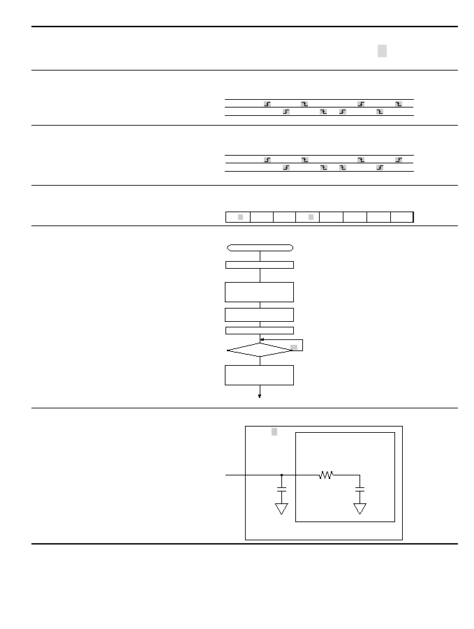
Section 13.3.4 Synchronouse
Operation
Figure 13.15 Sample Flowchart for
SCI Initialization
503
Figure amended
<Start transmitting or receiving>
(4)
(3)
(2)
(1)
Start of initialization
Yes
Wait
No
1-bit interval elapsed?
Set value in BRR
Clear TE and RE bits to 0 in SCR
Select communication format
in SMR
Set RIE, TIE, TEIE, MPIE, CKE1
and CKE0 bits in SCR (leaving
TE and RE bits cleared to 0)
Set TE or RE bit to 1 in SCR
Set RIE, TIE, TEIE, and MPIE
bits as necessary
(1)
(2)
(3)
(4)
Note:
*
Set the clock source in SCR. Clear the RIE,
TIE, TEIE, MPIE, TE, and RE bits to 0.
*
Select the communication format in SMR.
Write the value corresponding to the bit rate in
BRR.
This step is not necessary when an external
clock is used.
Wait for at least the interval required to transmit
or receive one bit, then set the TE or RE bit to
1 in SCR.
*
Set the RIE, TIE, TEIE, and MPIE
bits as necessary. Setting the TE or RE bit
enables the SCI to use the TxD or RxD pin.
In simultaneous transmitting and receiving,
the TE and RE bits should be cleared to 0 or
set to 1 simultaneously.
2nd
edition
Section 15.6 Usage Notes
Figure 15.11 Analog Input Circuit
(Example)
563
Figure amended
Equivalent circuit of
A/D converter
H8/3069F
20 pF
Cin =
15 pF
10 k
2nd
edition
Item
Page
Revisions (See Manual for Details)
Edition
Section 18.1 Features
There are two protection modes
577,
578
Note amended
*
Not available in the H8/3069F.
Description amended
� Programming/erasing time
The flash memory programming time is 3ms
(typ) in 128-byte simultaneous programming
and 25ms per byte. The erasing time is
1000ms (typ) per block.
� Number of programming
The number of flash memory programming
can be up to minimum 100 times.
2nd
edition
Section 18.2.2 Operating Mode
Table 18.1 Location of FWE and MD
Pins and Operating Modes
581
Pin name amended
RES
2nd
edition
Section 18.3 Pin Configuration
Table 18.3 Pin Configuration
587
Abbreviation name amended
RES
2nd
edition
Section 18.4.1 Registers
Table 18.5 Register/Parameter and
Target Mode
591
Table amended
FMATS
--
--
*
1
*
1
*
2
--
FTDAR
--
--
--
--
--
DPFR
--
--
--
--
--
FPFR
--
--
--
FPEFEQ
--
--
--
--
--
2nd
edition
Section 18.4.5 Flash Vector
Address Control Register (FVACR)
609,
610
Description amended
FVADRR to FVADRL
2nd
edition
Section 18.5.2 User Program Mode
Figure 18.10 RAM Map when
Programming/Erasing is Executed
617
Figure amended
FTDAR setting+2048
Area that can be
used by user
RAMEND(H'FFFF1F)
2nd
edition
Programming Procedure in User
Program Mode (c)
619
Description amended
NMI requests are discarded if the FVACR
register value is H'00. However, if H'80 has
been written to the FVACR register, they are
held and the NMI interrupts are generated
when processing returns to the user
procedure program.
2nd
edition
Programming Procedure in User
Program Mode (f)
620
Description amended
The current frequency of the CPU clock is set
to the FPEFEQ parameter (general register:
ER0).
2nd
edition
Item
Page
Revisions (See Manual for Details)
Edition
Section 18.5.2 User Program Mode
Programming Procedure in User
Program Mode (f)
621
Description amended
Not available in the H8/3069F, 0 must be set
to FUBRA.
2nd
edition
Programming Procedure in User
Program Mode (c) (f) (n)
623
Description amended
... byte units, and repeat steps (l) to (m).
2nd
edition
Section 18.5.3 User Boot Mode
User Boot Mode Initiation:
626
Description amended
To enable NMI interrupts in a user boot MAT
program, after the reset ends (
RES
= 1) and
TBD
�
s passes, set NMI to 1.
2nd
edition
Section 18.6.1 Hardware Protection
Table 18.9 Hardware Protection
631
Table amended
�
Resetting by means of the
RES
pin after
power is initially supplied will not make the
device enter the reset state unless the
RES
pin is held low until oscillation has
stabilized. In the case of a reset during
operation, hold the
RES
pin low for the
RES pulse width that is specified in the
section on AC characteristics section. If
the device is reset during programming or
erasure, data values in the flash memory
are not guaranteed. In this case, after
keeping the
RES
pin low for at least 100
�
s, execute erasure and then execute
programming again.
2nd
edition
Section 18.6.3 Error Protection
Figure 18.16 Transitions to and from
the Error-Protection State
633
Figure amended
Reset or standby
(Hardware protection)
Read disabled
Programming/erasing disabled
FLER=0
RES
= 0 or
STBY
= 0
Error occurrence
(Software standby)
RES
=0 or
STBY
=0
RES
=0 or
STBY
=0
Program/erase interface
register is in its initial state.
2nd
edition
Section 18.8.1 Usage Notes
1. Download time of on-chip program
638
Description amended
1. Download time of on-chip program
The programming program that includes the
initialization routine and the erasing program
that includes the initialization routine are each
2 kbytes or less. Accordingly, when the CPU
clock frequency is 25 MHz, the download for
each program takes approximately 164
�
s at
maximum.
2nd
edition
Item
Page
Revisions (See Manual for Details)
Edition
Section 18.9 PROM Mode
Table 18.11 PROM Mode Pin
639
Table newly added
2nd
edition
Section 18.9.2 PROM Mode
Operation
Table 18.13 Commands in PROM
Mode
642
Table amended
User MAT
write
X
H'20
write
X
H'20
User boot
MAT
write
X
H'25
H'25
2nd
edition
Section 18.9.4 Auto-Program Mode
(8)
643
Description amended
(8) Status-polling information on the I/O6 and
I/O7 pins is retained until the next
command is written. As long as no
command is written, the information is
made readable by setting
CE
and
OE
for
enabling.
2nd
edition
Section 18.9.5 Auto-Erase Mode
(4)
643
Description amended
(4) Status polling information on the I/O6 and
I/O7 pins is retained until the next
command writing. As long as no command
is written, the information is made
readable by setting
CE
and
OE
for
enabling.
2nd
edition
Section 18.10.1 Serial
Communication Interface
Specification for Boot Mode
� Communications Protocol
648
Description amended
(4) Programming of 128 bytes
2nd
edition
� Inquiry and Selection States
(7) User Boot MAT Information
Inquiry
(8) User MAT Information Inquiry
655
Description amended
Response
H'34
Size
A Number
of Areas
Area-Start Address
Area-Last Address
���
SUM
Area-Start Address (4 bytes) : Start address of the area
Area-Last Address (4 bytes) : Last address of the area
There are as many groups of data representing the start and last addresses as there are areas.
Response
H'35
Size
A Number
of Areas
Area-Start Address
Area-Last Address
���
SUM
Area-Start Address (4 bytes) : Start address of the area
Area-Last Address (4 bytes) : Last address of the area
There are as many groups of data representing the start and last addresses as there are areas.
2nd
edition

Item
Page
Revisions (See Manual for Details)
Edition
Section 18.10.1 Serial
Communication Interface
Specification for Boot Mode
� Inquiry and Selection States
(7) User Boot MAT Information
Inquiry
(8) User MAT Information Inquiry
655,
656
Description amended
Area-Start Address (4 bytes) : Start
address of the area
Area-Last Address (4 bytes) : Last
address of the area
Area-Start Address (4 bytes) : Start
address of the area
Area-Last Address (4 bytes) : Last
address of the area
2nd
edition
(11) New Bit-Rate Selection
657
Multiplication ratio 1 (1 byte) : The value
of multiplication or division ratios for the
main operating frequency
Multiplication ratio (1 byte) : The value
of the multiplication ratio (e.g. when
the clock frequency is multiplied by
four, the multiplication ratio will be
H'04. With this LSI it should be set to
H'01.)
Division ratio : The inverse of the
division ratio, as a negative number
(e.g. when the clock frequency is
divided by two, the value of division
ratio will be H'FE. H'FE = D'- 2. With
this LSI it should be set to H'01.)
Multiplication ratio 2 (1 byte) : The value of
multiplication or division ratios for the
peripheral frequency
Multiplication ratio (1 byte) : The value
of the multiplication ratio (e.g. when
the clock frequency is multiplied by
four, the multiplication ratio will be
H'04. With this LSI it should be set to
H'01.)
Division ratio : The inverse of the
division ratio, as a negative number
(e.g. when the clock is divided by two,
the value of division ratio will be H'FE.
H'FE = D'-2. With this LSI it should be
set to H'01.)
2nd
edition
Item
Page
Revisions (See Manual for Details)
Edition
Section 18.10.1 Serial
Communication Interface
Specification for Boot Mode
� Programming/erasing State
661
Description amended
A programming selection command makes
the boot program select the programming
method, an 128-byte programming command
makes it program the memory with data, and
an erasing selection command and block
erasing command make it erase the block.
2nd
edition
Section 18.10.2 AC Characteristics
and Timing in Writer Mode
Figure 18.33 Timing in Auto-Write
Mode
674
Figure amended
Address Stable
CE
FWE
A18-0
I/O5-0
I/O6
I/O7
OE
WE
t
as
t
ah
t
dh
t
ds
tf
tr
t
wep
t
wsts
t
write
t
spa
t
pns
t
pnh
t
nxtc
t
nxtc
t
ceh
t
ces
Identification Signal of
Programming Operation End
Data Transfer
1 byte to 128 bytes
Identification Signal of
Programming Operation
Successful End
H'40 or
H'45
1st byte
Din
128th byte
Din
H'00
2nd
edition
Figure 18.34 Timing in Auto-Erase
Mode
675
Figure amended
I/O5-0
H'20 or
H'25
H'20 or
H'25
H'00
2nd
edition
Section 18.10.3 Procedure Program
and Storable Area for Programming
Data
(6)
677
Description amended
The reset state (
RES
= 0) must be in place for
more than 100
�
s when the LSI mode is
changed to reset on completion of a
programming/erasing operation.
2nd
edition
Table 18.27 Executable MAT
678
Table amended
Initiated Mode
Operation
User Program Mode
User Boot Mode
*
Programming
Table 18.28 (1)
Table 18.28 (3)
Erasing
Table 18.28 (2)
Table 18.28 (4)
Note :
*
Programming/Erasing is possible to user MATs.
2nd
edition
Item
Page
Revisions (See Manual for Details)
Edition
Section 18.10.3 Procedure Program
and Storable Area for Programming
Data
Table 18.28 (2) Useable Area for
Erasure in User Program Mode
681
Table amended
Erasing
Procedure
Operation for
Selection of On-
chip Program to
be Downloaded
Operation for
Writing H'A5 to
Key Register
Execution of
Writing SC0 = 1
to FCCS
(Download)
Operation for
Key Register
Clear
Judgement of
Download Result
Operation for Download Error
2nd
edition
Table 18.28 (3) Useable Area for
Programming in User Boot Mode
683,
684
Table amended
Programming
procedure
Storage Area for
Program Data
Operation for
Selection of On-
chip Program to
be Downloaded
Operation for
Writing H'A5 to
Key Register
Execution of
Writing SC0 = 1
to FCCS
(Download)
Operation for
Key Register
Clear
Judgement of
Download Result
Operation for
Download Error
Switching MATs by FMATS
�
�
2nd
edition
Item
Page
Revisions (See Manual for Details)
Edition
Section 18.10.3 Procedure Program
and Storable Area for Programming
Data
Table 18.28 (4) Useable Area for
Erasure in User Boot Mode
685,
686
Table amended
Erasing
Procedure
Operation for
Selection of On-
chip Program to
be Downloaded
Operation for
Writing H'A5 to
Key Register
Execution of
Writing SC0 = 1
to FCCS
(Download)
Operation for
Key Register
Clear
Judgement of
Download Result
Operation for Download Error
Operation for Interrupt Inhibit
Switching MATs by FMATS
�
�
Operation for Writing H'5A to
Key Register
�
Operation for Settings of
Erasure Parameter
�
Execution of Erasure
�
�
Judgement of Erasure Result
�
Operation for Erasure Error
�
*
Operation for Key Register
Clear
�
Switching MATs by FMATS
�
�
Note:
*
Switching FMATS by a program in the on-chip RAM enables this area to be used.
2nd
edition
Section 19.2.2 External Clock Input
External Clock
Table 19.3 Clock Timing
691
Description amended
V
CC
= 5.0 V
�
10%
Item
Symbol Min
Max
Unit
Test Conditions
External clock input low
pulse width
t
EXL
15
--
ns
Figure 19.6
External clock input high
pulse width
t
EXH
15
--
ns
External clock rise time
t
EXr
--
5
ns
External clock fall time
t
EXf
--
5
ns
Clock low pulse width
t
CL
0.4
0.6
t
cyc
Figure 21.7
Clock high pulse width
t
CH
0.4
0.6
t
cyc
External clock output
settling delay time
t
DEXT
*
500
--
�
s
Figure 19.7
2nd
edition

Item
Page
Revisions (See Manual for Details)
Edition
Section 21.1.2 DC Characteristics
Table 21.2 DC Characteristics
712
Conditions amended
Conditions: V
CC
= AV
CC
= 5.0 V
�
10%, V
REF
=
4.5 V to AV
CC
*
1
, V
SS
= AV
SS
= 0
V
*
1
,
T
a
=�20
�
C to +75
�
C (Regular
specifications),
T
a
= �40
�
C to +85
�
C (Wide-range
specifications)
[Programming/erasing conditions:
T
a
= 0
�
C to +75
�
C (Regular
specifications),
T
a
= 0
�
C to +85
�
C (Wide-range
specifications)]
2nd
edition
713,
714
Table amanded
Current
dissipation
*
2
Normal
operation
I
CC
*
3
--
24
(5.0 V)
36
mA
f = 25 MHz
Sleep mode
--
20
(5.0 V)
33
mA
f = 25 MHz
Module
standby mode
--
15
(5.0 V)
25
mA
f = 25 MHz
Standby mode
--
25
(5.0 V)
90
�
A
T
a
50
�
C
--
--
120
�
A
50
�
C
<
T
a
Flash memory
programming/
erasing
*
4
--
34
(5.0 V)
46
mA
f = 25 MHz
Analog power
supply current
During A/D
conversion
AI
CC
--
0.9
1.5
mA
During A/D
and D/A
conversion
--
0.9
1.5
mA
Idle
--
0.05
(5.0 V)
5
�
A
T
a
50
�
C
at DASTE = 0
--
--
15
50
�
C
<
T
a
at DASTE = 0
�
A
Reference
current
During A/D
conversion
AI
CC
--
0.45
0.8
mA
During A/D
and D/A
conversion
--
1.8
3.0
mA
Idle
--
0.05
5.0
�
A
DASTE = 0
2nd
edition
Table 21.3 Permissible Output
Currents
715
Conditions amended
Conditions: V
CC
= AV
CC
= 5.0 V
�
10%, V
REF
=
4.5 V to AV
CC
, V
SS
= AV
SS
= 0 V,
T
a
= �20
�
C to +75
�
C (Regular
specifications),
T
a
= �40
�
C to +85
�
C (Wide-range
specifications)
2nd
edition

Item
Page
Revisions (See Manual for Details)
Edition
Section 21.1.3 AC Characteristics
Table 21.4 Clock Timing
Table 21.5 Control Signal Timing
Table 21.6 Bus Timing
Table 21.7 Timing of On-Chip
Supporting Modules
717,
718,
721
Conditions amended
Condition: T
a
= �20
�
C to +75
�
C (Regular
specifications),
T
a
= �40
�
C to +85
�
C (Wide-range
specifications)
V
CC
= AV
CC
= 5.0 V
�
10%, V
REF
=
4.5 to AV
CC
, V
SS
= AV
SS
= 0 V,
fmax = 25 MHz
2nd
edition
Section 21.1.4 A/D Conversion
Characteristics
Table 21.8 A/D Conversion
Characteristics
723
Conditions amended
Conditions: T
a
= �20
�
C to +75
�
C (Regular
specifications),
T
a
= �40
�
C to +85
�
C (Wide-range
specifications)
V
CC
= AV
CC
= 5.0 V
�
10%, V
REF
=
4.5 to AV
CC
, V
SS
= AV
SS
= 0 V,
fmax = 25 MHz
2nd
edition
Section 21.1.5 D/A Conversion
Characteristics
Table 21.9 D/A Conversion
Characteristics
724
Conditions amended
Conditions: T
a
= �20
�
C to +75
�
C (Regular
specifications),
T
a
= �40
�
C to +85
�
C (Wide-range
specifications)
V
CC
= AV
CC
= 5.0 V
�
10%, V
REF
=
4.5 to AV
CC
, V
SS
= AV
SS
= 0 V,
fmax = 25 MHz
2nd
edition
Item
Page
Revisions (See Manual for Details)
Edition
Section 21.1.6 Flash Memory
Characteristics
Table 21.10 Flash Memory
Characteristics
725
Conditions amended
Conditions: V
CC
= AV
CC
= 4.5 to 5.5 V, V
SS
=
AV
SS
= 0 V,
T
a
= 0
�
C to +75 (operating
temperature range for
programming/erasing : Regular
specifications)
T
a
= 0
�
C to +85 (operating
temperature range for
programming/erasing : Wide-
range specifications)
Table amended
Item
Symbol
Min
Typ
Max
Unit
Notes
Programming time
*
1,
*
2,
*
4
t
P
--
3
30
ms/
128 bytes
Erase time
*
1,
*
2,
*
4
t
E
--
80
800
ms/4k
blocks
--
500
5000
ms/32k
blocks
--
1000
10000 ms/64k
blocks
Programming time (total)
*
1,
*
2,
*
4
t
P
--
10
30
s/512k
bytes
T
a
= 25
�
C,
all "0"
Erase time (total)
*
1,
*
2,
*
4
t
E
--
10
30
s/512k
bytes
T
a
= 25
�
C
Programming and erase time (total)
*
1,
*
2,
*
4
t
PE
--
20
60
s/512k
bytes
T
a
= 25
�
C
Reprogramming count
N
WEC
100
*
3
--
--
times
Data retention time
*
4
t
DRP
10
--
--
year
Notes:
*
1 Programming and erase time depend on the data size.
*
2 Programming and erase time excluded the data transfer time.
*
3 It is the number of times of min. which guarantees all the characteristics after
reprogramming. (A guarantee is the range of a 1-min. value.)
*
4 It is the characteristic when reprogramming is performed by specification within the
limits including a min. value.
2nd
edition
B.3 Functions
MDCR--Mode Control Register
H'EE011
800
Description amended
Mode select 2 to 0
0
1
0
1
Operating Mode
Bit 2
MD
2
Bit 1
MD
1
Bit 0
MD
0
0
1
0
1
Mode 1
Mode 2
Mode 3
Mode 4
Mode 5
Mode 7
0
1
0
1
0
1
2nd
edition

i
Contents
Section 1 Overview .....................................................................
1
1.1
Overview ........................................................................................................
1
1.2
Block Diagram.................................................................................................
5
1.3
Pin Description................................................................................................
6
1.3.1
Pin Arrangement ...................................................................................
6
1.3.2
Pin Functions.......................................................................................
7
1.3.3
Pin Assignments in Each Mode ............................................................... 12
Section 2 CPU........................................................................... 17
2.1
Overview ........................................................................................................ 17
2.1.1
Features............................................................................................... 17
2.1.2
Differences from H8/300 CPU ................................................................. 18
2.2
CPU Operating Modes ...................................................................................... 19
2.3
Address Space .................................................................................................. 20
2.4
Register Configuration ...................................................................................... 21
2.4.1
Overview ............................................................................................. 21
2.4.2
General Registers .................................................................................. 22
2.4.3
Control Registers .................................................................................. 23
2.4.4
Initial CPU Register Values .................................................................... 24
2.5
Data Formats................................................................................................... 25
2.5.1
General Register Data Formats................................................................. 25
2.5.2
Memory Data Formats ........................................................................... 27
2.6
Instruction Set ................................................................................................. 28
2.6.1
Instruction Set Overview ........................................................................ 28
2.6.2
Instructions and Addressing Modes............................................................ 29
2.6.3
Tables of Instructions Classified by Function ............................................. 30
2.6.4
Basic Instruction Formats ....................................................................... 39
2.6.5
Notes on Use of Bit Manipulation Instructions ........................................... 40
2.7
Addressing Modes and Effective Address Calculation ............................................... 42
2.7.1
Addressing Modes.................................................................................. 42
2.7.2
Effective Address Calculation................................................................... 44
2.8
Processing States ............................................................................................. 48
2.8.1
Overview ............................................................................................. 48
2.8.2
Program Execution State ........................................................................ 49
2.8.3
Exception-Handling State........................................................................ 49
2.8.4
Exception-Handling Sequences ................................................................. 51
2.8.5
Bus-Released State................................................................................. 52
2.8.6
Reset State........................................................................................... 52
2.8.7
Power-Down State................................................................................. 52

ii
2.9
Basic Operational Timing ..................................................................................
53
2.9.1
Overview.............................................................................................
53
2.9.2
On-Chip Memory Access Timing ............................................................
53
2.9.3
On-Chip Supporting Module Access Timing..............................................
54
2.9.4
Access to External Address Space .............................................................
55
Section 3 MCU Operating Modes .................................................... 57
3.1
Overview........................................................................................................
57
3.1.1
Operating Mode Selection.......................................................................
57
3.1.2
Register Configuration........................................................................... 58
3.2
Mode Control Register (MDCR).........................................................................
59
3.3
System Control Register (SYSCR) .....................................................................
60
3.4
Operating Mode Descriptions ............................................................................. 62
3.4.1
Mode 1 ...............................................................................................
62
3.4.2
Mode 2 ...............................................................................................
62
3.4.3
Mode 3 ...............................................................................................
62
3.4.4
Mode 4 ...............................................................................................
63
3.4.5
Mode 5 ...............................................................................................
63
3.4.6
Mode 7 ...............................................................................................
63
3.5
Pin Functions in Each Operating Mode ................................................................
64
3.6
Memory Map in Each Operating Mode.................................................................
65
3.6.1
Note on Reserved Areas..........................................................................
65
Section 4 Exception Handling......................................................... 71
4.1
Overview........................................................................................................
71
4.1.1
Exception Handling Types and Priority ..................................................... 71
4.1.2
Exception Handling Operation.................................................................
71
4.1.3
Exception Vector Table ..........................................................................
72
4.2
Reset ............................................................................................................. 74
4.2.1
Overview.............................................................................................
74
4.2.2
Reset Sequence .....................................................................................
74
4.2.3
Interrupts after Reset..............................................................................
76
4.3
Interrupts........................................................................................................
77
4.4
Trap Instruction ...............................................................................................
78
4.5
Stack Status after Exception Handling.................................................................. 79
4.6
Notes on Stack Usage .......................................................................................
80
Section 5 Interrupt Controller ......................................................... 83
5.1
Overview........................................................................................................
83
5.1.1
Features ..............................................................................................
83
5.1.2
Block Diagram .....................................................................................
84
5.1.3
Pin Configuration .................................................................................
85
5.1.4
Register Configuration........................................................................... 85

iii
5.2
Register Descriptions ........................................................................................ 86
5.2.1
System Control Register (SYSCR) .......................................................... 86
5.2.2
Interrupt Priority Registers A and B (IPRA, IPRB) ...................................... 87
5.2.3
IRQ Status Register (ISR) ...................................................................... 94
5.2.4
IRQ Enable Register (IER)...................................................................... 95
5.2.5
IRQ Sense Control Register (ISCR) ......................................................... 96
5.3
Interrupt Sources .............................................................................................. 97
5.3.1
External Interrupts ................................................................................. 97
5.3.2
Internal Interrupts .................................................................................. 98
5.3.3
Interrupt Vector Table ............................................................................ 98
5.4
Interrupt Operation ........................................................................................... 102
5.4.1
Interrupt Handling Process ...................................................................... 102
5.4.2
Interrupt Sequence ................................................................................. 107
5.4.3
Interrupt Response Time......................................................................... 108
5.5
Usage Notes .................................................................................................... 109
5.5.1
Contention between Interrupt and Interrupt-Disabling Instruction.................... 109
5.5.2
Instructions that Inhibit Interrupts ............................................................ 110
5.5.3
Interrupts during EEPMOV Instruction Execution ....................................... 110
Section 6 Bus Controller ...............................................................111
6.1
Overview ........................................................................................................ 111
6.1.1
Features............................................................................................... 111
6.1.2
Block Diagram...................................................................................... 113
6.1.3
Pin Configuration ................................................................................. 114
6.1.4
Register Configuration ........................................................................... 115
6.2
Register Descriptions ........................................................................................ 116
6.2.1
Bus Width Control Register (ABWCR) ..................................................... 116
6.2.2
Access State Control Register (ASTCR).................................................... 117
6.2.3
Wait Control Registers H and L (WCRH, WCRL) ...................................... 117
6.2.4
Bus Release Control Register (BRCR) ...................................................... 121
6.2.5
Bus Control Register (BCR).................................................................... 122
6.2.6
Chip Select Control Register (CSCR)....................................................... 126
6.2.7
DRAM Control Register A (DRCRA) ...................................................... 127
6.2.8
DRAM Control Register B (DRCRB) ....................................................... 129
6.2.9
Refresh Timer Control/Status Register (RTMCSR) ..................................... 131
6.2.10 Refresh Timer Counter (RTCNT)............................................................. 133
6.2.11 Refresh Time Constant Register (RTCOR) ................................................ 133
6.2.12 Address Control Register (ADRCR).......................................................... 134
6.3
Operation........................................................................................................ 135
6.3.1
Area Division ....................................................................................... 135
6.3.2
Bus Specifications ................................................................................. 137
6.3.3
Memory Interfaces ................................................................................. 138
6.3.4
Chip Select Signals ............................................................................... 139

iv
6.3.5
Address Output Method .......................................................................... 140
6.4
Basic Bus Interface ........................................................................................... 142
6.4.1
Overview............................................................................................. 142
6.4.2
Data Size and Data Alignment................................................................. 142
6.4.3
Valid Strobes ...................................................................................... 143
6.4.4
Memory Areas...................................................................................... 144
6.4.5
Basic Bus Control Signal Timing ............................................................ 146
6.4.6
Wait Control........................................................................................ 153
6.5
DRAM Interface .............................................................................................. 155
6.5.1
Overview............................................................................................. 155
6.5.2
DRAM Space and
RAS Output Pin Settings.............................................. 155
6.5.3
Address Multiplexing............................................................................. 156
6.5.4
Data Bus ............................................................................................. 157
6.5.5
Pins Used for DRAM Interface ................................................................ 157
6.5.6
Basic Timing ....................................................................................... 158
6.5.7
Precharge State Control.......................................................................... 159
6.5.8
Wait Control........................................................................................ 160
6.5.9
Byte Access Control and
CAS Output Pin ................................................. 161
6.5.10 Burst Operation .................................................................................... 163
6.5.11 Refresh Control .................................................................................... 168
6.5.12 Examples of Use................................................................................... 172
6.5.13 Usage Notes......................................................................................... 176
6.6
Interval Timer ................................................................................................. 179
6.6.1
Operation ............................................................................................ 179
6.7
Interrupt Sources.............................................................................................. 184
6.8
Burst ROM Interface......................................................................................... 184
6.8.1
Overview............................................................................................. 184
6.8.2
Basic Timing ....................................................................................... 184
6.8.3
Wait Control........................................................................................ 185
6.9
Idle Cycle ....................................................................................................... 186
6.9.1
Operation ............................................................................................ 186
6.9.2
Pin States in Idle Cycle.......................................................................... 189
6.10 Bus Arbiter ..................................................................................................... 190
6.10.1 Operation ............................................................................................ 190
6.11 Register and Pin Input Timing ........................................................................... 193
6.11.1 Register Write Timing ........................................................................... 193
6.11.2
BREQ Pin Input Timing........................................................................ 194
Section 7 DMA Controller............................................................. 195
7.1
Overview........................................................................................................ 195
7.1.1
Features .............................................................................................. 195
7.1.2
Block Diagram ..................................................................................... 196
7.1.3
Functional Overview ............................................................................. 197

v
7.1.4
Input/Output Pins ................................................................................. 198
7.1.5
Register Configuration ........................................................................... 198
7.2
Register Descriptions (1) (Short Address Mode)...................................................... 200
7.2.1
Memory Address Registers (MAR) ........................................................... 200
7.2.2
I/O Address Registers (IOAR) .................................................................. 201
7.2.3
Execute Transfer Count Registers (ETCR) ................................................. 201
7.2.4
Data Transfer Control Registers (DTCR) ................................................... 203
7.3
Register Descriptions (2) (Full Address Mode) ....................................................... 206
7.3.1
Memory Address Registers (MAR) ........................................................... 206
7.3.2
I/O Address Registers (IOAR) .................................................................. 206
7.3.3
Execute Transfer Count Registers (ETCR) ................................................. 207
7.3.4
Data Transfer Control Registers (DTCR) ................................................... 209
7.4
Operation........................................................................................................ 215
7.4.1
Overview ............................................................................................. 215
7.4.2
I/O Mode ............................................................................................. 217
7.4.3
Idle Mode............................................................................................. 219
7.4.4
Repeat Mode ........................................................................................ 222
7.4.5
Normal Mode ....................................................................................... 225
7.4.6
Block Transfer Mode .............................................................................. 228
7.4.7
DMAC Activation................................................................................. 233
7.4.8
DMAC Bus Cycle ................................................................................. 235
7.4.9
Multiple-Channel Operation .................................................................... 241
7.4.10 External Bus Requests, DRAM Interface, and DMAC................................... 242
7.4.11 NMI Interrupts and DMAC ..................................................................... 243
7.4.12 Aborting a DMAC Transfer..................................................................... 244
7.4.13 Exiting Full Address Mode...................................................................... 245
7.4.14 DMAC States in Reset State, Standby Modes, and Sleep Mode...................... 246
7.5
Interrupts ........................................................................................................ 247
7.6
Usage Notes .................................................................................................... 248
7.6.1
Note on Word Data Transfer .................................................................... 248
7.6.2
DMAC Self-Access ............................................................................... 248
7.6.3
Longword Access to Memory Address Registers .......................................... 248
7.6.4
Note on Full Address Mode Setup ............................................................ 248
7.6.5
Note on Activating DMAC by Internal Interrupts ........................................ 249
7.6.6
NMI Interrupts and Block Transfer Mode.................................................... 250
7.6.7
Memory and I/O Address Register Values................................................... 250
7.6.8
Bus Cycle when Transfer is Aborted.......................................................... 251
7.6.9
Transfer Requests by A/D Converter ......................................................... 251
Section 8 I/O Ports ......................................................................253
8.1
Overview ........................................................................................................ 253
8.2
Port 1 ............................................................................................................ 256
8.2.1
Overview ............................................................................................. 256

vi
8.2.2
Register Descriptions............................................................................. 257
8.3
Port 2 ............................................................................................................ 259
8.3.1
Overview............................................................................................. 259
8.3.2
Register Descriptions............................................................................. 260
8.4
Port 3 ............................................................................................................ 263
8.4.1
Overview............................................................................................. 263
8.4.2
Register Descriptions............................................................................. 263
8.5
Port 4 ............................................................................................................ 265
8.5.1
Overview............................................................................................. 265
8.5.2
Register Descriptions............................................................................. 266
8.6
Port 5 ............................................................................................................ 269
8.6.1
Overview............................................................................................. 269
8.6.2
Register Descriptions............................................................................. 269
8.7
Port 6 ............................................................................................................ 273
8.7.1
Overview............................................................................................. 273
8.7.2
Register Descriptions............................................................................. 274
8.8
Port 7 ............................................................................................................ 277
8.8.1
Overview............................................................................................. 277
8.8.2
Register Description .............................................................................. 278
8.9
Port 8 ............................................................................................................ 279
8.9.1
Overview............................................................................................. 279
8.9.2
Register Descriptions............................................................................. 281
8.10 Port 9 ............................................................................................................ 285
8.10.1 Overview............................................................................................. 285
8.10.2 Register Descriptions............................................................................. 286
8.11 Port A ........................................................................................................... 290
8.11.1 Overview............................................................................................. 290
8.11.2 Register Descriptions............................................................................. 292
8.12 Port B............................................................................................................ 301
8.12.1 Overview............................................................................................. 301
8.12.2 Register Descriptions............................................................................. 303
Section 9 16-Bit Timer................................................................. 311
9.1
Overview........................................................................................................ 311
9.1.1
Features .............................................................................................. 311
9.1.2
Block Diagrams .................................................................................... 313
9.1.3
Pin Configuration ................................................................................. 316
9.1.4
Register Configuration........................................................................... 317
9.2
Register Descriptions........................................................................................ 318
9.2.1
Timer Start Register (TSTR)................................................................... 318
9.2.2
Timer Synchro Register (TSNC).............................................................. 319
9.2.3
Timer Mode Register (TMDR) ................................................................ 320
9.2.4
Timer Interrupt Status Register A (TISRA)................................................ 323

vii
9.2.5
Timer Interrupt Status Register B (TISRB)................................................. 326
9.2.6
Timer Interrupt Status Register C (TISRC) ................................................ 329
9.2.7
Timer Counters (16TCNT)...................................................................... 331
9.2.8
General Registers (GRA, GRB)................................................................ 332
9.2.9
Timer Control Registers (16TCR) ............................................................ 333
9.2.10 Timer I/O Control Register (TIOR) .......................................................... 335
9.2.11 Timer Output Level Setting Register C (TOLR) ......................................... 337
9.3
CPU Interface .................................................................................................. 339
9.3.1
16-Bit Accessible Registers ..................................................................... 339
9.3.2
8-Bit Accessible Registers....................................................................... 341
9.4
Operation........................................................................................................ 342
9.4.1
Overview ............................................................................................. 342
9.4.2
Basic Functions .................................................................................... 342
9.4.3
Synchronization .................................................................................... 350
9.4.4
PWM Mode ......................................................................................... 352
9.4.5
Phase Counting Mode ............................................................................ 356
9.4.6
16-Bit Timer Output Timing ................................................................... 358
9.5
Interrupts ........................................................................................................ 359
9.5.1
Setting of Status Flags........................................................................... 359
9.5.2
Timing of Clearing of Status Flags .......................................................... 361
9.5.3
Interrupt Sources ................................................................................... 362
9.6
Usage Notes .................................................................................................... 363
Section 10 8-Bit Timers ................................................................375
10.1 Overview ........................................................................................................ 375
10.1.1 Features............................................................................................... 375
10.1.2 Block Diagram...................................................................................... 377
10.1.3 Pin Configuration ................................................................................. 378
10.1.4 Register Configuration ........................................................................... 379
10.2 Register Descriptions ........................................................................................ 380
10.2.1 Timer Counters (8TCNT) ....................................................................... 380
10.2.2 Time Constant Registers A (TCORA)....................................................... 381
10.2.3 Time Constant Registers B (TCORB) ....................................................... 382
10.2.4 Timer Control Register (8TCR) ............................................................... 383
10.2.5 Timer Control/Status Registers (8TCSR) .................................................. 386
10.3 CPU Interface .................................................................................................. 391
10.3.1 8-Bit Registers...................................................................................... 391
10.4 Operation........................................................................................................ 393
10.4.1 8TCNT Count Timing ........................................................................... 393
10.4.2 Compare Match Timing ......................................................................... 394
10.4.3 Input Capture Signal Timing................................................................... 395
10.4.4 Timing of Status Flag Setting ................................................................. 396
10.4.5 Operation with Cascaded Connection......................................................... 397

viii
10.4.6 Input Capture Setting ............................................................................ 400
10.5 Interrupt ......................................................................................................... 401
10.5.1 Interrupt Sources................................................................................... 401
10.5.2 A/D Converter Activation....................................................................... 402
10.6 8-Bit Timer Application Example ....................................................................... 402
10.7 Usage Notes.................................................................................................... 403
10.7.1 Contention between 8TCNT Write and Clear.............................................. 403
10.7.2 Contention between 8TCNT Write and Increment........................................ 404
10.7.3 Contention between TCOR Write and Compare Match................................. 405
10.7.4 Contention between TCOR Read and Input Capture..................................... 406
10.7.5 Contention between Counter Clearing by Input Capture and Counter Increment 407
10.7.6 Contention between TCOR Write and Input Capture.................................... 408
10.7.7 Contention between 8TCNT Byte Write and Increment in 16-Bit Count Mode
(Cascaded Connection) ........................................................................... 409
10.7.8 Contention between Compare Matches A and B .......................................... 410
10.7.9 8TCNT Operation and Internal Clock Source Switchover.............................. 410
Section 11 Programmable Timing Pattern Controller (TPC) ...................... 413
11.1 Overview........................................................................................................ 413
11.1.1 Features .............................................................................................. 413
11.1.2 Block Diagram ..................................................................................... 414
11.1.3 TPC Pins ............................................................................................ 415
11.1.4 Registers ............................................................................................. 416
11.2 Register Descriptions........................................................................................ 417
11.2.1 Port A Data Direction Register (PADDR).................................................. 417
11.2.2 Port A Data Register (PADR) ................................................................. 417
11.2.3 Port B Data Direction Register (PBDDR) .................................................. 418
11.2.4 Port B Data Register (PBDR) .................................................................. 418
11.2.5 Next Data Register A (NDRA) ................................................................ 419
11.2.6 Next Data Register B (NDRB) ................................................................. 421
11.2.7 Next Data Enable Register A (NDERA) .................................................... 423
11.2.8 Next Data Enable Register B (NDERB) .................................................... 424
11.2.9 TPC Output Control Register (TPCR)...................................................... 425
11.2.10 TPC Output Mode Register (TPMR) ........................................................ 428
11.3 Operation ....................................................................................................... 430
11.3.1 Overview............................................................................................. 430
11.3.2 Output Timing ..................................................................................... 431
11.3.3 Normal TPC Output.............................................................................. 432
11.3.4 Non-Overlapping TPC Output................................................................. 434
11.3.5 TPC Output Triggering by Input Capture .................................................. 436
11.4 Usage Notes.................................................................................................... 437
11.4.1 Operation of TPC Output Pins ................................................................ 437
11.4.2 Note on Non-Overlapping Output ............................................................ 437

ix
Section 12 Watchdog Timer............................................................439
12.1 Overview ........................................................................................................ 439
12.1.1 Features............................................................................................... 439
12.1.2 Block Diagram...................................................................................... 440
12.1.3 Register Configuration ........................................................................... 440
12.2 Register Descriptions ........................................................................................ 441
12.2.1 Timer Counter (TCNT) .......................................................................... 441
12.2.2 Timer Control/Status Register (TCSR) ..................................................... 442
12.2.3 Reset Control/Status Register (RSTCSR).................................................. 444
12.2.4 Notes on Register Access........................................................................ 445
12.3 Operation........................................................................................................ 447
12.3.1 Watchdog Timer Operation...................................................................... 447
12.3.2 Interval Timer Operation......................................................................... 448
12.3.3 Timing of Setting of Overflow Flag (OVF)................................................ 449
12.3.4 Timing of Setting of Watchdog Timer Reset Bit (WRST)............................. 450
12.4 Interrupts ........................................................................................................ 451
12.5 Usage Notes .................................................................................................... 451
Section 13 Serial Communication Interface ..........................................453
13.1 Overview ........................................................................................................ 453
13.1.1 Features............................................................................................... 453
13.1.2 Block Diagram...................................................................................... 455
13.1.3 Input/Output Pins ................................................................................. 456
13.1.4 Register Configuration ........................................................................... 457
13.2 Register Descriptions ........................................................................................ 458
13.2.1 Receive Shift Register (RSR).................................................................. 458
13.2.2 Receive Data Register (RDR) .................................................................. 458
13.2.3 Transmit Shift Register (TSR)................................................................. 459
13.2.4 Transmit Data Register (TDR) ................................................................. 459
13.2.5 Serial Mode Register (SMR) ................................................................... 460
13.2.6 Serial Control Register (SCR) ................................................................. 464
13.2.7 Serial Status Register (SSR) ................................................................... 469
13.2.8 Bit Rate Register (BRR) ......................................................................... 474
13.3 Operation........................................................................................................ 483
13.3.1 Overview ............................................................................................. 483
13.3.2 Operation in Asynchronous Mode............................................................. 485
13.3.3 Multiprocessor Communication ............................................................... 495
13.3.4 Synchronous Operation .......................................................................... 501
13.4 SCI Interrupts.................................................................................................. 510
13.5 Usage Notes .................................................................................................... 510
13.5.1 Notes on Use of SCI.............................................................................. 510

x
Section 14 Smart Card Interface ...................................................... 517
14.1 Overview........................................................................................................ 517
14.1.1 Features .............................................................................................. 517
14.1.2 Block Diagram ..................................................................................... 518
14.1.3 Pin Configuration ................................................................................. 518
14.1.4 Register Configuration........................................................................... 519
14.2 Register Descriptions........................................................................................ 520
14.2.1 Smart Card Mode Register (SCMR) ......................................................... 520
14.2.2 Serial Status Register (SSR) ................................................................... 521
14.2.3 Serial Mode Register (SMR) ................................................................... 523
14.2.4 Serial Control Register (SCR)................................................................. 524
14.3 Operation ....................................................................................................... 524
14.3.1 Overview............................................................................................. 524
14.3.2 Pin Connections ................................................................................... 525
14.3.3 Data Format......................................................................................... 526
14.3.4 Register Settings .................................................................................. 527
14.3.5 Clock ................................................................................................. 529
14.3.6 Transmitting and Receiving Data ............................................................. 531
14.4 Usage Notes.................................................................................................... 539
Section 15 A/D Converter ............................................................. 543
15.1 Overview........................................................................................................ 543
15.1.1 Features .............................................................................................. 543
15.1.2 Block Diagram ..................................................................................... 544
15.1.3 Input Pins ........................................................................................... 545
15.1.4 Register Configuration........................................................................... 546
15.2 Register Descriptions........................................................................................ 547
15.2.1 A/D Data Registers A to D (ADDRA to ADDRD)...................................... 547
15.2.2 A/D Control/Status Register (ADCSR)..................................................... 548
15.2.3 A/D Control Register (ADCR) ................................................................ 551
15.3 CPU Interface.................................................................................................. 552
15.4 Operation ....................................................................................................... 553
15.4.1 Single Mode (SCAN = 0) ....................................................................... 553
15.4.2 Scan Mode (SCAN = 1) ......................................................................... 555
15.4.3 Input Sampling and A/D Conversion Time ................................................ 557
15.4.4 External Trigger Input Timing................................................................. 558
15.5 Interrupts........................................................................................................ 559
15.6 Usage Notes.................................................................................................... 559
Section 16 D/A Converter ............................................................. 565
16.1 Overview........................................................................................................ 565
16.1.1 Features .............................................................................................. 565
16.1.2 Block Diagram ..................................................................................... 565

xi
16.1.3 Input/Output Pins ................................................................................. 566
16.1.4 Register Configuration ........................................................................... 566
16.2 Register Descriptions ........................................................................................ 567
16.2.1 D/A Data Registers 0 and 1 (DADR0/1) .................................................... 567
16.2.2 D/A Control Register (DACR) ................................................................ 567
16.2.3 D/A Standby Control Register (DASTCR)................................................. 569
16.3 Operation........................................................................................................ 570
16.4 D/A Output Control ......................................................................................... 571
Section 17 RAM.........................................................................573
17.1 Overview ........................................................................................................ 573
17.1.1 Block Diagram...................................................................................... 573
17.1.2 Register Configuration ........................................................................... 574
17.2 System Control Register (SYSCR) ..................................................................... 574
17.3 Operation........................................................................................................ 575
Section 18 ROM.........................................................................577
18.1 Features.......................................................................................................... 577
18.2 Overview ........................................................................................................ 579
18.2.1 Block Diagram...................................................................................... 579
18.2.2 Operating Mode .................................................................................... 580
18.2.3 Mode Comparison ................................................................................. 581
18.2.4 Flash MAT Configuration ...................................................................... 582
18.2.5 Block Division ..................................................................................... 583
18.2.6 Programming/Erasing Interface ................................................................ 584
18.3 Pin Configuration ............................................................................................ 587
18.4 Register Configuration ...................................................................................... 588
18.4.1 Registers ............................................................................................. 588
18.4.2 Programming/Erasing Interface Register .................................................... 591
18.4.3 Programming/Erasing Interface Parameter .................................................. 597
18.4.4 RAM Control Register (RAMCR) ........................................................... 608
18.4.5 Flash Vector Address Control Register (FVACR)........................................ 609
18.4.6 Flash Vector Address Data Register (FVADR) ............................................ 611
18.5 On-Board Programming Mode............................................................................. 612
18.5.1 Boot Mode ........................................................................................... 612
18.5.2 User Program Mode ............................................................................... 615
18.5.3 User Boot Mode .................................................................................... 626
18.6 Protection ....................................................................................................... 630
18.6.1 Hardware Protection ............................................................................... 630
18.6.2 Software Protection ............................................................................... 631
18.6.3 Error Protection .................................................................................... 632
18.7 Flash Memory Emulation in RAM...................................................................... 634
18.8 Switching between User MAT and User Boot MAT................................................ 637

xii
18.8.1 Usage Notes......................................................................................... 638
18.9 PROM Mode .................................................................................................. 639
18.9.1 Pin Arrangement of the Socket Adapter..................................................... 639
18.9.2 PROM Mode Operation ......................................................................... 641
18.9.3 Memory-Read Mode .............................................................................. 642
18.9.4 Auto-Program Mode .............................................................................. 642
18.9.5 Auto-Erase Mode .................................................................................. 643
18.9.6 Status-Read Mode ................................................................................. 644
18.9.7 Status Polling ...................................................................................... 644
18.9.8 Time Taken in Transition to PROM Mode ................................................ 645
18.9.9 Notes on Using PROM Mode ................................................................. 645
18.10 Further Information .......................................................................................... 646
18.10.1 Serial Communication Interface Specification for Boot Mode ........................ 646
18.10.2 AC Characteristics and Timing in Writer Mode........................................... 671
18.10.3 Procedure Program and Storable Area for Programming Data ......................... 677
Section 19 Clock Pulse Generator .................................................... 687
19.1 Overview........................................................................................................ 687
19.1.1 Block Diagram ..................................................................................... 687
19.2 Oscillator Circuit ............................................................................................. 688
19.2.1 Connecting a Crystal Resonator............................................................... 688
19.2.2 External Clock Input ............................................................................. 690
19.3 Duty Adjustment Circuit ................................................................................... 692
19.4 Prescalers ....................................................................................................... 692
19.5 Frequency Divider ............................................................................................ 692
19.5.1 Register Configuration........................................................................... 693
19.5.2 Division Control Register (DIVCR) ......................................................... 693
19.5.3 Usage Notes......................................................................................... 694
Section 20 Power-Down State ........................................................ 695
20.1 Overview........................................................................................................ 695
20.2 Register Configuration...................................................................................... 697
20.2.1 System Control Register (SYSCR) .......................................................... 697
20.2.2 Module Standby Control Register H (MSTCRH) ........................................ 699
20.2.3 Module Standby Control Register L (MSTCRL)......................................... 700
20.3 Sleep Mode..................................................................................................... 702
20.3.1 Transition to Sleep Mode ....................................................................... 702
20.3.2 Exit from Sleep Mode............................................................................ 702
20.4 Software Standby Mode..................................................................................... 703
20.4.1 Transition to Software Standby Mode ....................................................... 703
20.4.2 Exit from Software Standby Mode............................................................ 703
20.4.3 Selection of Waiting Time for Exit from Software Standby Mode .................. 704
20.4.4 Sample Application of Software Standby Mode .......................................... 705

xiii
20.4.5 Note ................................................................................................... 705
20.5 Hardware Standby Mode..................................................................................... 706
20.5.1 Transition to Hardware Standby Mode ....................................................... 706
20.5.2 Exit from Hardware Standby Mode............................................................ 706
20.5.3 Timing for Hardware Standby Mode .......................................................... 706
20.5.4 Timing for Hardware Standby Mode at Power-On ........................................ 707
20.6 Module Standby Function .................................................................................. 708
20.6.1 Module Standby Timing ......................................................................... 708
20.6.2 Read/Write in Module Standby................................................................. 708
20.6.3 Usage Notes ......................................................................................... 708
20.7 System Clock Output Disabling Function ............................................................ 709
Section 21 Electrical Characteristics...................................................711
21.1 Electrical Characteristics of H8/3069F-ZTAT ........................................................ 711
21.1.1 Absolute Maximum Ratings ................................................................... 711
21.1.2 DC Characteristics................................................................................. 712
21.1.3 AC Characteristics................................................................................. 717
21.1.4 A/D Conversion Characteristics ............................................................... 723
21.1.5 D/A Conversion Characteristics ............................................................... 724
21.1.6 Flash Memory Characteristics.................................................................. 725
21.2 Operational Timing .......................................................................................... 726
21.2.1 Clock Timing....................................................................................... 726
21.2.2 Control Signal Timing........................................................................... 727
21.2.3 Bus Timing.......................................................................................... 728
21.2.4 DRAM Interface Bus Timing................................................................... 734
21.2.5 TPC and I/O Port Timing ....................................................................... 737
21.2.6 Timer Input/Output Timing .................................................................... 738
21.2.7 SCI Input/Output Timing ....................................................................... 739
21.2.8 DMAC Timing..................................................................................... 740
Appendix A Instruction Set ............................................................741
A.1
Instruction List ................................................................................................ 741
A.2
Operation Code Maps........................................................................................ 756
A.3
Number of States Required for Execution .............................................................. 759
Appendix B Internal I/O Registers ....................................................768
B.1
Addresses (EMC = 1) ........................................................................................ 768
B.2
Addresses (EMC = 0) ........................................................................................ 781
B.3
Functions ....................................................................................................... 794
Appendix C I/O Port Block Diagrams ............................................... .889
C.1
Port 1 Block Diagram ....................................................................................... 889
C.2
Port 2 Block Diagram ....................................................................................... 890

xiv
C.3
Port 3 Block Diagram ....................................................................................... 891
C.4
Port 4 Block Diagram ....................................................................................... 892
C.5
Port 5 Block Diagram ....................................................................................... 893
C.6
Port 6 Block Diagrams...................................................................................... 894
C.7
Port 7 Block Diagrams...................................................................................... 901
C.8
Port 8 Block Diagrams...................................................................................... 902
C.9
Port 9 Block Diagrams...................................................................................... 907
C.10 Port A Block Diagrams ..................................................................................... 913
C.11 Port B Block Diagrams ..................................................................................... 916
Appendix D Pin States ................................................................. 924
D.1
Port States in Each Mode .................................................................................. 924
D.2
Pin States at Reset ........................................................................................... 931
Appendix E Timing of Transition to and Recovery from Hardware Standby
Mode ...................................................................... 934
Appendix F Product Code Lineup.................................................... 935
Appendix G Package Dimensions .................................................... 936
Appendix H Comparison of H8/300H Series Product Specifications. . . . . . . . . . . . 938
H.1
Differences between H8/3069F, H8/3067 Series and H8/3062 Series, H8/3048 Series,
H8/3007 and H8/3006, and H8/3002.................................................................... 938
H.2
Comparison of Pin Functions of 100-Pin Package Products (FP-100B, TFP-100B)..... 942

1
Section 1 Overview
1.1
Overview
The H8/3069F is a series of microcontrollers (MCUs) that integrate system supporting functions
together with an H8/300H CPU core having an original Hitachi architecture.
The H8/300H CPU has a 32-bit internal architecture with sixteen 16-bit general registers, and a
concise, optimized instruction set designed for speed. It can address a 16-Mbyte linear address
space. Its instruction set is upward-compatible at the object-code level with the H8/300 CPU,
enabling easy porting of software from the H8/300 Series.
The on-chip system supporting functions include ROM, RAM, a 16-bit timer, an 8-bit timer, a
programmable timing pattern controller (TPC), a watchdog timer (WDT), a serial communication
interface (SCI), an A/D converter, a D/A converter, I/O ports, a direct memory access controller
(DMAC), and other facilities.
The H8/3069F has 512 kbytes of flash memory and 16 kbytes of RAM.
Six MCU operating modes offer a choice of bus width and address space size. The modes (modes
1 to 5, 7) include one single-chip mode and five expanded modes.
The H8/3069F includes an F-ZTATTM* version with on-chip flash memory that can be
programmed on-board. This version enables users to respond quickly and flexibly to changing
application specifications, growing production volumes, and other conditions.
Table 1.1 summarizes the features of the H8/3069F.
Note: * F-ZTATTM (Flexible ZTAT) is a trademark of Hitachi, Ltd.

2
Table 1.1
Features
Feature
Description
CPU
Upward-compatible with the H8/300 CPU at the object-code level
General-register machine
�
Sixteen 16-bit general registers
(also usable as sixteen 8-bit registers, eight 16-bit registers, or eight 32-bit
registers)
High-speed operation
�
Maximum clock rate: 25 MHz
�
Add/subtract: 80 ns
�
Multiply/divide: 560 ns
16-Mbyte address space
Instruction features
�
8/16/32-bit data transfer, arithmetic, and logic instructions
�
Signed and unsigned multiply instructions (8 bits x 8 bits, 16 bits x 16 bits)
�
Signed and unsigned divide instructions (16 bits
�
8 bits, 32 bits
�
16 bits)
�
Bit accumulator function
�
Bit manipulation instructions with register-indirect specification of bit
positions
Memory
H8/3069F
�
ROM: 512 kbytes
�
RAM: 16 kbytes
Interrupt
controller
�
Seven external interrupt pins: NMI,
IRQ
0
to
IRQ
5
�
36 internal interrupts
�
Three selectable interrupt priority levels
Bus controller
�
Address space can be partitioned into eight areas, with independent bus
specifications in each area
�
Chip select output available for areas 0 to 7
�
8-bit access or 16-bit access selectable for each area
�
Two-state or three-state access selectable for each area
�
Selection of two wait modes
�
Number of program wait states selectable for each area
�
Direct connection of burst ROM
�
Direct connection of up to 8-Mbyte DRAM (or DRAM interface can be used
as interval timer)
�
Bus arbitration function

3
Feature
Description
DMA controller
(DMAC)
Short address mode
�
Maximum four channels available
�
Selection of I/O mode, idle mode, or repeat mode
�
Can be activated by compare match/input capture A interrupts from 16-bit
timer channels 0 to 2, conversion-end interrupts from the A/D converter,
transmit-data-empty and receive-data-full interrupts from the SCI, or external
requests
Full address mode
�
Maximum two channels available
�
Selection of normal mode or block transfer mode
�
Can be activated by compare match/input capture A interrupts from 16-bit
timer channels 0 to 2, conversion-end interrupts from the A/D converter,
external requests, or auto-request
16-bit timer,
3 channels
�
Three 16-bit timer channels, capable of processing up to six pulse outputs or
six pulse inputs
�
16-bit timer counter (channels 0 to 2)
�
Two multiplexed output compare/input capture pins (channels 0 to 2)
�
Operation can be synchronized (channels 0 to 2)
�
PWM mode available (channels 0 to 2)
�
Phase counting mode available (channel 2)
�
DMAC can be activated by compare match/input capture A interrupts
(channels 0 to 2)
8-bit timer,
4 channels
�
8-bit up-counter (external event count capability)
�
Two time constant registers
�
Two channels can be connected
Programmable
timing pattern
controller (TPC)
�
Maximum 16-bit pulse output, using 16-bit timer as time base
�
Up to four 4-bit pulse output groups (or one 16-bit group, or two 8-bit groups)
�
Non-overlap mode available
�
Output data can be transferred by DMAC
Watchdog
timer (WDT),
1 channel
�
Reset signal can be generated by overflow
�
Usable as an interval timer
Serial
communication
interface (SCI),
3 channels
�
Selection of asynchronous or synchronous mode
�
Full duplex: can transmit and receive simultaneously
�
On-chip baud-rate generator
�
Smart card interface functions added

4
Feature
Description
A/D converter
�
Resolution: 10 bits
�
Eight channels, with selection of single or scan mode
�
Variable analog conversion voltage range
�
Sample-and-hold function
�
A/D conversion can be started by an external trigger or 8-bit timer compare-
match
�
DMAC can be activated by an A/D conversion end interrupt
D/A converter
�
Resolution: 8 bits
�
Two channels
�
D/A outputs can be sustained in software standby mode
I/O ports
�
70 input/output pins
�
9 input-only pins
Operating modes
�
Six MCU operating modes
Mode
Address Space
Address Pins
Initial Bus Width
Max. Bus Width
Mode 1
1 Mbyte
A
19
to A
0
8 bits
16 bits
Mode 2
1 Mbyte
A
19
to A
0
16 bits
16 bits
Mode 3
16 Mbytes
A
23
to A
0
8 bits
16 bits
Mode 4
16 Mbytes
A
23
to A
0
16 bits
16 bits
Mode 5
16 Mbytes
A
23
to A
0
8 bits
16 bits
Mode 7
1 Mbyte
--
--
--
�
On-chip ROM is disabled in modes 1 to 4
Power-down
state
�
Sleep mode
�
Software standby mode
�
Hardware standby mode
�
Module standby function
�
Programmable system clock frequency division
Other features
�
On-chip clock pulse generator
Product lineup
Product Type
Product Code
Package
Classification
H8/3069 F-ZTAT
HD64F3069F
100-pin QFP (FP-100B)
On-chip flash
HD64F3069TE
100-pin TQFP (TFP-100B) memory
5
1.2
Block Diagram
Figure 1.1 shows an internal block diagram.
V
V
V
V
V
V
V
V
V
CC
CC
SS
SS
SS
SS
SS
SS
CL
P3 /D
P3 /D
P3 /D
P3 /D
P3 /D
P3 /D
P3 /D
P3 /D
7
6
5
4
3
2
1
0
P4 /D
P4 /D
P4 /D
P4 /D
P4 /D
P4 /D
P4 /D
P4 /D
7
6
5
4
3
2
1
0
7
6
5
4
3
2
1
0
Port 3
Port 4
Port 5
Port 9
P5 /A
P5 /A
P5 /A
P5 /A
3
2
1
0
19
18
17
16
P2 /A
P2 /A
P2 /A
P2 /A
P2 /A
P2 /A
P2 /A
P2 /A
7
6
5
4
3
2
1
0
P9 /SCK /IRQ
P9 /SCK /IRQ
P9 /RxD
P9 /RxD
P9 /TxD
P9 /TxD
5
4
3
2
1
0
1
0
1
0
1
0
5
4
DA
1
/AN
7
/P7
7
DA
0
/AN
6
/P7
6
AN
5
/P7
5
AN
4
/P7
4
AN
3
/P7
3
AN
2
/P7
2
AN
1
/P7
1
AN
0
/P7
0
Port 7
A
20
/TIOCB
2
/TP
7
/PA
7
A
21
/TIOCA
2
/TP
6
/PA
6
A
22
/TIOCB
1
/TP
5
/PA
5
A
23
/TIOCA
1
/TP
4
/PA
4
TCLKD/TIOCB
0
/TP
3
/PA
3
TCLKC/TIOCA
0
/TP
2
/PA
2
TEND
1
/TCLKB/TP
1
/PA
1
TEND
0
/TCLKA/TP
0
/PA
0
Port A
RxD
2
/TP
15
/PB
7
TxD
2
/TP
14
/PB
6
SCK
2
/LCAS/TP
13
/PB
5
UCAS/TP
12
/PB
4
CS
4
/DREQ
1
/TMIO
3
/TP
11
/PB
3
CS
5
/TMO
2
/TP
10
/PB
2
CS
6
/DREQ
0
/TMIO
1
/TP
9
/PB
1
CS
7
/TMO
0
/TP
8
/PB
0
Port 8
CS
0
/P8
4
ADTRG/CS
1
/IRQ
3
/P8
3
CS
2
/IRQ
2
/P8
2
CS
3
/IRQ
1
/P8
1
RFSH/IRQ
0
/P8
0
MD
2
MD
1
MD
0
EXTAL
XTAL
STBY
RES
FWE
NMI
H8/300H CPU
Clock pulse
generator
Interrupt controller
ROM
(flash memory)
DMA controller
(DMAC)
Serial communication
interface
(SCI) 3 channels
�
Watchdog timer
(WDT)
15
14
13
12
11
10
9
8
Address bus
Data bus (upper)
Data bus (lower)
15
14
13
12
11
10
9
8
Port 2
P1 /A
P1 /A
P1 /A
P1 /A
P1 /A
P1 /A
P1 /A
P1 /A
7
6
5
4
3
2
1
0
Port 1
7
6
5
4
3
2
1
0
/P6
7
LWR/P6
6
HWR/P6
5
RD/P6
4
AS/P6
3
BACK/P6
2
BREQ/P6
1
WAIT/P6
0
RAM
16-bit timer unit
8-bit timer unit
A/D converter
D/A converter
Port 6
Bus controller
Programmable
timing pattern
controller (TPC)
Port B
V
REF
AV
CC
AV
SS
Figure 1.1 Block Diagram
6
1.3
Pin Description
1.3.1
Pin Arrangement
The pin arrangement of the H8/3069F FP-100B and TFP-100B packages is shown in figure 1.2.
V
CL
*
CS
7
/TMO
0
/TP
8
/PB
0
CS
6
/DREQ
0
/TMIO
1
/TP
9
/PB
1
CS
5
/TMO
2
/TP
10
/PB
2
CS
4
/DREQ
1
/TMIO
3
/TP
11
/PB
3
UCAS/TP
12
/PB
4
SCK
2
/LCAS/TP
13
/PB
5
TxD
2
/TP
14
/PB
6
RxD
2
/TP
15
/PB
7
0
1
2
3
4
5
0
1
2
3
4
5
6
FWE
V
SS
TxD /P9
TxD /P9
RxD /P9
RxD /P9
IRQ /SCK /P9
IRQ /SCK /P9
D /P4
D /P4
D /P4
D /P4
D /P4
D /P4
D /P4
MD
MD
MD
P6 /L
WR
P6 /HWR
P6 /RD
P6 /AS
V
XT
AL
EXT
AL
V
NMI
RES
STBY
P6
7
/
P6 /BACK
P6 /BREQ
P6 /W
AIT
V
P5 /A
P5 /A
P5 /A
P5 /A
P2 /A
P2 /A
1
2
3
4
5
6
7
8
9
10
11
12
13
14
15
16
17
18
19
20
21
22
23
24
25
74
73
75
72
71
70
69
68
67
66
65
64
63
62
61
60
59
58
57
56
55
54
53
52
51
50
49
48
47
46
45
44
43
42
41
40
39
38
37
36
35
34
33
32
31
30
29
28
27
26
P2
5
/A
13
P2
4
/A
12
P2
3
/A
11
P2
2
/A
10
P2
1
/A
9
P2
0
/A
8
V
SS
P1
7
/A
7
P1
6
/A
6
P1
5
/A
5
P1
4
/A
4
P1
3
/A
3
P1
2
/A
2
P1
1
/A
1
P1
0
/A
0
V
CC
P3
7
/D
15
P3
6
/D
14
P3
5
/D
13
P3
4
/D
12
P3
3
/D
11
P3
2
/D
10
P3
1
/D
9
P3
0
/D
8
P4
7
/D
7
76
77
78
79
80
81
82
83
84
85
86
87
88
89
90
91
92
93
94
95
96
97
98
99
100
AV
CC
V
REF
AN
0
/P7
0
AN
1
/P7
1
AN
2
/P7
2
AN
3
/P7
3
AN
4
/P7
4
AN
5
/P7
5
AN
6
/DA
0
/P7
6
AN
7
/DA
1
/P7
7
AV
SS
IRQ
0
/RFSH/P8
0
IRQ
1
/CS
3
/P8
1
IRQ
2
/CS
2
/P8
2
IRQ
3
/CS
1
/ADTRG/P8
3
CS
0
/P8
4
V
SS
TP
0
/TCLKA/TEND
0
/PA
0
TP
1
/TCLKB/TEND
1
/PA
1
TP
2
/TIOCA
0
/TCLKC/PA
2
TP
3
/TIOCB
0
/TCLKD/PA
3
TP
4
/TIOCA
1
/A
23
/PA
4
TP
5
/TIOCB
1
/A
22
/PA
5
TP
6
/TIOCA
2
/A
21
/PA
6
TP
7
/TIOCB
2
/A
20
/PA
7
0
1
0
1
0
1
0
1
2
3
4
5
6
4
5
2
1
0
2
1
0
3
2
1
0
7
6
Top view
(FP-100B, TFP-100B)
6
5
4
3
CC
SS
SS
19
18
17
16
15
14
V
SS
Note:
*
When functioning as V
CL
pin, the connection of an external capacitor is required.
1
0.1
�
F
Figure 1.2 Pin Arrangement (FP-100B or TFP-100B, Top View)

7
1.3.2
Pin Functions
Table 1.2 summarizes the pin functions.
Table 1.2
Pin Functions
Pin No.
Type
Symbol
FP-100B
TFP-100B
I/O
Name and Function
Power
V
CC
35, 68
Input
Power: For connection to the power supply. Connect
all V
CC
pins to the system power supply.
V
SS
11, 22, 44,
57, 65, 92
Input
Ground: For connection to ground (0 V).
Connect all V
SS
pins to the 0-V system power supply.
Internal
step-down
pin
V
CL
1
Output
Connect an external capacitor between this pin and
GND (0 V). Do not connect to V
CC
.
V
CL
0.1
�
F
Clock
XTAL
67
Input
For connection to a crystal resonator.
For examples of crystal resonator and external clock
input, see section 19, Clock Pulse Generator.
EXTAL
66
Input
For connection to a crystal resonator or input of an
external clock signal. For examples of crystal
resonator and external clock input, see section 19,
Clock Pulse Generator.
61
Output
System clock: Supplies the system clock to external
devices.

8
Pin No.
Type
Symbol
FP-100B
TFP-100B
I/O
Name and Function
Operating
mode
control
MD
2
to
MD
0
75 to 73
Input
Mode 2 to mode 0: For setting the operating mode,
as follows. The H8/3069F can be used only in modes
1 to 5, 7. The inputs at the mode pins must select
one of these six modes. The inputs at the mode pins
must not be changed during operation. Inputs at
these pins must not be changed during operation.
MD
2
MD
1
MD
0
Operating Mode
0
0
0
--
0
0
1
Mode 1
0
1
0
Mode 2
0
1
1
Mode 3
1
0
0
Mode 4
1
0
1
Mode 5
1
1
0
--
1
1
1
Mode 7
System
control
RES
63
Input
Reset input: When driven low, this pin resets the
chip
FWE
10
Input
Write enable signal: Flash memory write control
signal
STBY
62
Input
Standby: When driven low, this pin forces a
transition to hardware standby mode
BREQ
59
Input
Bus request: Used by an external bus master to
request the bus right
BACK
60
Output
Bus request acknowledge: Indicates that the bus
has been granted to an external bus master
Interrupts
NMI
64
Input
Nonmaskable interrupt: Requests a
nonmaskable interrupt
IRQ
5
to
IRQ
0
17, 16,
90 to 87
Input
Interrupt request 5 to 0: Maskable interrupt request
pins
Address
bus
A
23
to A
0
97 to 100,
56 to 45,
43 to 36
Output
Address bus: Outputs address signals

9
Pin No.
Type
Symbol
FP-100B
TFP-100B
I/O
Name and Function
Data bus
D
15
to D
0
34 to 23,
21 to 18
Input/
output
Data bus: Bidirectional data bus
Bus control
CS
7
to
CS
0
2 to 5,
88 to 91
Output
Chip select: Select signals for areas 7 to 0
AS
69
Output
Address strobe: Goes low to indicate valid address
output on the address bus
RD
70
Output
Read: Goes low to indicate reading from the external
address space
HWR
71
Output
High write: Goes low to indicate writing to the
external address space; indicates valid data on the
upper data bus (D
15
to D
8
).
LWR
72
Output
Low write: Goes low to indicate writing to the
external address space; indicates valid data on the
lower data bus (D
7
to D
0
).
WAIT
58
Input
Wait: Requests insertion of wait states in bus cycles
during access to the external address space
DRAM
RFSH
87
Output
Refresh: Indicates a refresh cycle
interface
CS
2
to
CS
5
89, 88,
5, 4
Output
Row address strobe
RAS
: Row address strobe
signal for DRAM
RD
70
Output
Write enable
WE
: Write enable signal for DRAM
HWR
UCAS
71
6
Output
Upper column address strobe
UCAS
: Column
address strobe signal for DRAM
LWR
LCAS
72
7
Output
Lower column address strobe
LCAS
: Column
address strobe signal for DRAM
DMA
controller
DREQ
1
,
DREQ
0
5, 3
Input
DMA request 1 and 0: DMAC activation
requests
(DMAC)
TEND
1
,
TEND
0
94, 93
Output
Transfer end 1 and 0: These signals indicate that
the DMAC has ended a data transfer

10
Pin No.
Type
Symbol
FP-100B
TFP-100B
I/O
Name and Function
16-bit timer TCLKD to
TCLKA
96 to 93
Input
Clock input D to A: External clock inputs
TIOCA
2
to
TIOCA
0
99, 97, 95
Input/
output
Input capture/output compare A2 to A0: GRA2 to
GRA0 output compare or input capture, or PWM
output
TIOCB
2
to
TIOCB
0
100, 98,
96
Input/
output
Input capture/output compare B2 to B0: GRB2 to
GRB0 output compare or input capture, or PWM
output
8-bit timer
TMO
0
,
TMO
2
2, 4
Output
Compare match output: Compare match output
pins
TMIO
1
,
TMIO
3
3, 5
Input/
output
Input capture input/compare match output: Input
capture input or compare match output pins
TCLKD to
TCLKA
96 to 93
Input
Counter external clock input: These pins input an
external clock to the counters.
Program-
mable
timing
pattern
controller
(TPC)
TP
15
to
TP
0
9 to 2,
100 to 93
Output
TPC output 15 to 0: Pulse output
Serial com-
munication
TxD
2
to
TxD
0
8, 13, 12
Output
Transmit data (channels 0, 1, 2): SCI data output
interface
(SCI)
RxD
2
to
RxD
0
9, 15, 14
Input
Receive data (channels 0, 1, 2): SCI data input
SCK
2
to
SCK
0
7, 17, 16
Input/
output
Serial clock (channels 0, 1, 2): SCI clock
input/output
A/D
converter
AN
7
to
AN
0
85 to 78
Input
Analog 7 to 0: Analog input pins
ADTRG
90
Input
A/D conversion external trigger input: External
trigger input for starting A/D conversion
D/A
converter
DA
1
, DA
0
85, 84
Output
Analog output: Analog output from the
D/A converter

11
Pin No.
Type
Symbol
FP-100B
TFP-100B
I/O
Name and Function
A/D and
D/A
converters
AV
CC
76
Input
Power supply pin for the A/D and D/A converters.
Connect to the system power supply when not using
the A/D and D/A converters.
AV
SS
86
Input
Ground pin for the A/D and D/A converters. Connect
to system ground (0 V).
V
REF
77
Input
Reference voltage input pin for the A/D and D/A
converters. Connect to the system power supply
when not using the A/D and D/A converters.
I/O ports
P1
7
to P1
0
43 to 36
Input/
output
Port 1: Eight input/output pins. The direction of each
pin can be selected in the port 1 data direction
register (P1DDR).
P2
7
to P2
0
52 to 45
Input/
output
Port 2: Eight input/output pins. The direction of each
pin can be selected in the port 2 data direction
register (P2DDR).
P3
7
to P3
0
34 to 27
Input/
output
Port 3: Eight input/output pins. The direction of each
pin can be selected in the port 3 data direction
register (P3DDR).
P4
7
to P4
0
26 to 23,
21 to 18
Input/
output
Port 4: Eight input/output pins. The direction of each
pin can be selected in the port 4 data direction
register (P4DDR).
P5
3
to P5
0
56 to 53
Input/
output
Port 5: Four input/output pins. The direction of each
pin can be selected in the port 5 data direction
register (P5DDR).
P6
7
to P6
0
61,
72 to 69,
60 to 58
Input/
output
Port 6: Seven input/output pins and one input pin.
The direction of each pin can be selected in the port
6 data direction register (P6DDR).
P7
7
to P7
0
85 to 78
Input
Port 7: Eight input pins
P8
4
to P8
0
91 to 87
Input/
output
Port 8: Five input/output pins. The direction of each
pin can be selected in the port 8 data direction
register (P8DDR).
P9
5
to P9
0
17 to 12
Input/
output
Port 9: Six input/output pins. The direction of each
pin can be selected in the port 9 data direction
register (P9DDR).
PA
7
to PA
0
100 to 93
Input/
output
Port A: Eight input/output pins. The direction of each
pin can be selected in the port A data direction
register (PADDR).
PB
7
to PB
0
9 to 2
Input/
output
Port B: Eight input/output pins. The direction of each
pin can be selected in the port B data direction
register (PBDDR).

12
1.3.3
Pin Assignments in Each Mode
Table 1.3 lists the pin assignments in each mode.
Table 1.3
Pin Assignments in Each Mode (FP-100B or TFP-100B)
Pin No.
Pin Name
FP-100B
TFP-100B
Mode 1
Mode 2
Mode 3
Mode 4
Mode 5
Mode 7
1
V
CL
V
CL
V
CL
V
CL
V
CL
V
CL
2
PB
0
/TP
8
/
TMO
0
/
CS
7
PB
0
/TP
8
/
TMO
0
/
CS
7
PB
0
/TP
8
/
TMO
0
/
CS
7
PB
0
/TP
8
/
TMO
0
/
CS
7
PB
0
/TP
8
/
TMO
0
/
CS
7
PB
0
/TP
8
/
TMO
0
3
PB
1
/TP
9
/
TMIO
1
/
DREQ
0
/
CS
6
PB
1
/TP
9
/
TMIO
1
/
DREQ
0
/
CS
6
PB
1
/TP
9
/
TMIO
1
/
DREQ
0
/
CS
6
PB
1
/TP
9
/
TMIO
1
/
DREQ
0
/
CS
6
PB
1
/TP
9
/
TMIO
1
/
DREQ
0
/
CS
6
PB
1
/TP
9
/
TMIO
1
/
DREQ
0
4
PB
2
/TP
10
/
TMO
2
/
CS
5
PB
2
/TP
10
/
TMO
2
/
CS
5
PB
2
/TP
10
/
TMO
2
/
CS
5
PB
2
/TP
10
/
TMO
2
/
CS
5
PB
2
/TP
10
/
TMO
2
/
CS
5
PB
2
/TP
10
/
TMO
2
5
PB
3
/TP
11
/
TMIO
3
/
DREQ
1
/
CS
4
PB
3
/TP
11
/
TMIO
3
/
DREQ
1
/
CS
4
PB
3
/TP
11
/
TMIO
3
/
DREQ
1
/
CS
4
PB
3
/TP
11
/
TMIO
3
/
DREQ
1
/
CS
4
PB
3
/TP
11
/
TMIO
3
/
DREQ
1
/
CS
4
PB
3
/TP
11
/
TMIO
3
/
DREQ
1
6
PB
4
/TP
12
/
UCAS
PB
4
/TP
12
/
UCAS
PB
4
/TP
12
/
UCAS
PB
4
/TP
12
/
UCAS
PB
4
/TP
12
/
UCAS
PB
4
/TP
12
7
PB
5
/TP
13
/
LCAS
/
SCK
2
PB
5
/TP
13
/
LCAS
/
SCK
2
PB
5
/TP
13
/
LCAS
/
SCK
2
PB
5
/TP
13
/
LCAS
/
SCK
2
PB
5
/TP
13
/
LCAS
/
SCK
2
PB
5
/TP
13
/
SCK
2
8
PB
6
/TP
14
/
TxD
2
PB
6
/TP
14
/
TxD
2
PB
6
/TP
14
/
TxD
2
PB
6
/TP
14
/
TxD
2
PB
6
/TP
14
/
TxD
2
PB
6
/TP
14
/
TxD
2
9
PB
7
/TP
15
/
RxD
2
PB
7
/TP
15
/
RxD
2
PB
7
/TP
15
/
RxD
2
PB
7
/TP
15
/
RxD
2
PB
7
/TP
15
/
RxD
2
PB
7
/TP
15
/
RxD
2
10
FWE
FWE
FWE
FWE
FWE
FWE
11
V
SS
V
SS
V
SS
V
SS
V
SS
V
SS
12
P9
0
/TxD
0
P9
0
/TxD
0
P9
0
/TxD
0
P9
0
/TxD
0
P9
0
/TxD
0
P9
0
/TxD
0
13
P9
1
/TxD
1
P9
1
/TxD
1
P9
1
/TxD
1
P9
1
/TxD
1
P9
1
/TxD
1
P9
1
/TxD
1
14
P9
2
/RxD
0
P9
2
/RxD
0
P9
2
/RxD
0
P9
2
/RxD
0
P9
2
/RxD
0
P9
2
/RxD
0
15
P9
3
/RxD
1
P9
3
/RxD
1
P9
3
/RxD
1
P9
3
/RxD
1
P9
3
/RxD
1
P9
3
/RxD
1
16
P9
4
/
IRQ
4
/
SCK
0
P9
4
/
IRQ
4
/
SCK
0
P9
4
/
IRQ
4
/
SCK
0
P9
4
/
IRQ
4
/
SCK
0
P9
4
/
IRQ
4
/
SCK
0
P9
4
/
IRQ
4
/
SCK
0
17
P9
5
/
IRQ
5
/
SCK
1
P9
5
/
IRQ
5
/
SCK
1
P9
5
/
IRQ
5
/
SCK
1
P9
5
/
IRQ
5
/
SCK
1
P9
5
/
IRQ
5
/
SCK
1
P9
5
/
IRQ
5
/
SCK
1
18
P4
0
/D
0
*
1
P4
0
/D
0
*
2
P4
0
/D
0
*
1
P4
0
/D
0
*
2
P4
0
/D
0
*
1
P4
0
19
P4
1
/D
1
*
1
P4
1
/D
1
*
2
P4
1
/D
1
*
1
P4
1
/D
1
*
2
P4
1
/D
1
*
1
P4
1
20
P4
2
/D
2
*
1
P4
2
/D
2
*
2
P4
2
/D
2
*
1
P4
2
/D
2
*
2
P4
2
/D
2
*
1
P4
2

13
Pin No.
Pin Name
FP-100B
TFP-100B
Mode 1
Mode 2
Mode 3
Mode 4
Mode 5
Mode 7
21
P4
3
/D
3
*
1
P4
3
/D
3
*
2
P4
3
/D
3
*
1
P4
3
/D
3
*
2
P4
3
/D
3
*
1
P4
3
22
V
SS
V
SS
V
SS
V
SS
V
SS
V
SS
23
P4
4
/D
4
*
1
P4
4
/D
4
*
2
P4
4
/D
4
*
1
P4
4
/D
4
*
2
P4
4
/D
4
*
1
P4
4
24
P4
5
/D
5
*
1
P4
5
/D
5
*
2
P4
5
/D
5
*
1
P4
5
/D
5
*
2
P4
5
/D
5
*
1
P4
5
25
P4
6
/D
6
*
1
P4
6
/D
6
*
2
P4
6
/D
6
*
1
P4
6
/D
6
*
2
P4
6
/D
6
*
1
P4
6
26
P4
7
/D
7
*
1
P4
7
/D
7
*
2
P4
7
/D
7
*
1
P4
7
/D
7
*
2
P4
7
/D
7
*
1
P4
7
27
D
8
D
8
D
8
D
8
D
8
P3
0
28
D
9
D
9
D
9
D
9
D
9
P3
1
29
D
10
D
10
D
10
D
10
D
10
P3
2
30
D
11
D
11
D
11
D
11
D
11
P3
3
31
D
12
D
12
D
12
D
12
D
12
P3
4
32
D
13
D
13
D
13
D
13
D
13
P3
5
33
D
14
D
14
D
14
D
14
D
14
P3
6
34
D
15
D
15
D
15
D
15
D
15
P3
7
35
V
CC
V
CC
V
CC
V
CC
V
CC
V
CC
36
A
0
A
0
A
0
A
0
P1
0
/A
0
P1
0
37
A
1
A
1
A
1
A
1
P1
1
/A
1
P1
1
38
A
2
A
2
A
2
A
2
P1
2
/A
2
P1
2
39
A
3
A
3
A
3
A
3
P1
3
/A
3
P1
3
40
A
4
A
4
A
4
A
4
P1
4
/A
4
P1
4
41
A
5
A
5
A
5
A
5
P1
5
/A
5
P1
5
42
A
6
A
6
A
6
A
6
P1
6
/A
6
P1
6
43
A
7
A
7
A
7
A
7
P1
7
/A
7
P1
7
44
V
SS
V
SS
V
SS
V
SS
V
SS
V
SS
45
A
8
A
8
A
8
A
8
P2
0
/A
8
P2
0
46
A
9
A
9
A
9
A
9
P2
1
/A
9
P2
1
47
A
10
A
10
A
10
A
10
P2
2
/A
10
P2
2
48
A
11
A
11
A
11
A
11
P2
3
/A
11
P2
3
49
A
12
A
12
A
12
A
12
P2
4
/A
12
P2
4
50
A
13
A
13
A
13
A
13
P2
5
/A
13
P2
5
51
A
14
A
14
A
14
A
14
P2
6
/A
14
P2
6
52
A
15
A
15
A
15
A
15
P2
7
/A
15
P2
7
53
A
16
A
16
A
16
A
16
P5
0
/A
16
P5
0
54
A
17
A
17
A
17
A
17
P5
1
/A
17
P5
1

14
Pin No.
Pin Name
FP-100B
TFP-100B
Mode 1
Mode 2
Mode 3
Mode 4
Mode 5
Mode 7
55
A
18
A
18
A
18
A
18
P5
2
/A
18
P5
2
56
A
19
A
19
A
19
A
19
P5
3
/A
19
P5
3
57
V
SS
V
SS
V
SS
V
SS
V
SS
V
SS
58
P6
0
/
WAIT
P6
0
/
WAIT
P6
0
/
WAIT
P6
0
/
WAIT
P6
0
/
WAIT
P6
0
59
P6
1
/
BREQ
P6
1
/
BREQ
P6
1
/
BREQ
P6
1
/
BREQ
P6
1
/
BREQ
P6
1
60
P6
2
/
BACK
P6
2
/
BACK
P6
2
/
BACK
P6
2
/
BACK
P6
2
/
BACK
P6
2
61
P6
7
/
*
3
P6
7
/
*
3
P6
7
/
*
3
P6
7
/
*
3
P6
7
/
*
3
P6
7
/
*
4
62
STBY
STBY
STBY
STBY
STBY
STBY
63
RES
RES
RES
RES
RES
RES
64
NMI
NMI
NMI
NMI
NMI
NMI
65
V
SS
V
SS
V
SS
V
SS
V
SS
V
SS
66
EXTAL
EXTAL
EXTAL
EXTAL
EXTAL
EXTAL
67
XTAL
XTAL
XTAL
XTAL
XTAL
XTAL
68
V
CC
V
CC
V
CC
V
CC
V
CC
V
CC
69
AS
AS
AS
AS
AS
P6
3
70
RD
RD
RD
RD
RD
P6
4
71
HWR
HWR
HWR
HWR
HWR
P6
5
72
LWR
LWR
LWR
LWR
LWR
P6
6
73
MD
0
MD
0
MD
0
MD
0
MD
0
MD
0
74
MD
1
MD
1
MD
1
MD
1
MD
1
MD
1
75
MD
2
MD
2
MD
2
MD
2
MD
2
MD
2
76
AV
CC
AV
CC
AV
CC
AV
CC
AV
CC
AV
CC
77
V
REF
V
REF
V
REF
V
REF
V
REF
V
REF
78
P7
0
/AN
0
P7
0
/AN
0
P7
0
/AN
0
P7
0
/AN
0
P7
0
/AN
0
P7
0
/AN
0
79
P7
1
/AN
1
P7
1
/AN
1
P7
1
/AN
1
P7
1
/AN
1
P7
1
/AN
1
P7
1
/AN
1
80
P7
2
/AN
2
P7
2
/AN
2
P7
2
/AN
2
P7
2
/AN
2
P7
2
/AN
2
P7
2
/AN
2
81
P7
3
/AN
3
P7
3
/AN
3
P7
3
/AN
3
P7
3
/AN
3
P7
3
/AN
3
P7
3
/AN
3
82
P7
4
/AN
4
P7
4
/AN
4
P7
4
/AN
4
P7
4
/AN
4
P7
4
/AN
4
P7
4
/AN
4
83
P7
5
/AN
5
P7
5
/AN
5
P7
5
/AN
5
P7
5
/AN
5
P7
5
/AN
5
P7
5
/AN
5
84
P7
6
/AN
6
/
DA
0
P7
6
/AN
6
/
DA
0
P7
6
/AN
6
/
DA
0
P7
6
/AN
6
/
DA
0
P7
6
/AN
6
/
DA
0
P7
6
/AN
6
/
DA
0
85
P7
7
/AN
7
/
DA
1
P7
7
/AN
7
/
DA
1
P7
7
/AN
7
/
DA
1
P7
7
/AN
7
/
DA
1
P7
7
/AN
7
/
DA
1
P7
7
/AN
7
/
DA
1
86
AV
SS
AV
SS
AV
SS
AV
SS
AV
SS
AV
SS

15
Pin No.
Pin Name
FP-100B
TFP-100B
Mode 1
Mode 2
Mode 3
Mode 4
Mode 5
Mode 7
87
P8
0
/
IRQ
0
/
RFSH
P8
0
/
IRQ
0
/
RFSH
P8
0
/
IRQ
0
/
RFSH
P8
0
/
IRQ
0
/
RFSH
P8
0
/
IRQ
0
/
RFSH
P8
0
/
IRQ
0
88
P8
1
/
IRQ
1
/
CS
3
P8
1
/
IRQ
1
/
CS
3
P8
1
/
IRQ
1
/
CS
3
P8
1
/
IRQ
1
/
CS
3
P8
1
/
IRQ
1
/
CS
3
P8
1
/
IRQ
1
89
P8
2
/
IRQ
2
/
CS
2
P8
2
/
IRQ
2
/
CS
2
P8
2
/
IRQ
2
/
CS
2
P8
2
/
IRQ
2
/
CS
2
P8
2
/
IRQ
2
/
CS
2
P8
2
/
IRQ
2
90
P8
3
/
IRQ
3
/
CS
1
/
ADTRG
P8
3
/
IRQ
3
/
CS
1
/
ADTRG
P8
3
/
IRQ
3
/
CS
1
/
ADTRG
P8
3
/
IRQ
3
/
CS
1
/
ADTRG
P8
3
/
IRQ
3
/
CS
1
/
ADTRG
P8
3
/
IRQ
3
/
ADTRG
91
P8
4
/
CS
0
P8
4
/
CS
0
P8
4
/
CS
0
P8
4
/
CS
0
P8
4
/
CS
0
P8
4
92
V
SS
V
SS
V
SS
V
SS
V
SS
V
SS
93
PA
0
/TP
0
/
TCLKA/
TEND
0
PA
0
/TP
0
/
TCLKA/
TEND
0
PA
0
/TP
0
/
TCLKA/
TEND
0
PA
0
/TP
0
/
TCLKA/
TEND
0
PA
0
/TP
0
/
TCLKA/
TEND
0
PA
0
/TP
0
/
TCLKA/
TEND
0
94
PA
1
/TP
1
/
TCLKB/
TEND
1
PA
1
/TP
1
/
TCLKB/
TEND
1
PA
1
/TP
1
/TCLKB/
TEND
1
PA
1
/TP
1
/
TCLKB/
TEND
1
PA
1
/TP
1
/
TCLKB/
TEND
1
PA
1
/TP
1
/
TCLKB/
TEND
1
95
PA
2
/TP
2
/
TIOCA
0
/
TCLKC
PA
2
/TP
2
/
TIOCA
0
/
TCLKC
PA
2
/TP
2
/
TIOCA
0
/
TCLKC
PA
2
/TP
2
/
TIOCA
0
/
TCLKC
PA
2
/TP
2
/
TIOCA
0
/
TCLKC
PA
2
/TP
2
/
TIOCA
0
/
TCLKC
96
PA
3
/TP
3
/
TIOCB
0
/
TCLKD
PA
3
/TP
3
/
TIOCB
0
/
TCLKD
PA
3
/TP
3
/
TIOCB
0
/
TCLKD
PA
3
/TP
3
/
TIOCB
0
/
TCLKD
PA
3
/TP
3
/
TIOCB
0
/
TCLKD
PA
3
/TP
3
/
TIOCB
0
/
TCLKD
97
PA
4
/TP
4
/
TIOCA
1
PA
4
/TP
4
/
TIOCA
1
PA
4
/TP
4
/
TIOCA
1
/
A
23
PA
4
/TP
4
/
TIOCA
1
/
A
23
PA
4
/TP
4
/
TIOCA
1
/
A
23
PA
4
/TP
4
/
TIOCA
1
98
PA
5
/TP
5
/
TIOCB
1
PA
5
/TP
5
/
TIOCB
1
PA
5
/TP
5
/
TIOCB
1
/
A
22
PA
5
/TP
5
/
TIOCB
1
/
A
22
PA
5
/TP
5
/
TIOCB
1
/
A
22
PA
5
/TP
5
/
TIOCB
1
99
PA
6
/TP
6
/
TIOCA
2
PA
6
/TP
6
/
TIOCA
2
PA
6
/TP
6
/
TIOCA
2
/
A
21
PA
6
/TP
6
/
TIOCA
2
/
A
21
PA
6
/TP
6
/
TIOCA
2
/
A
21
PA
6
/TP
6
/
TIOCA
2
100
PA
7
/TP
7
/
TIOCB
2
PA
7
/TP
7
/
TIOCB
2
A
20
A
20
PA
7
/TP
7
/
TIOCB
2
/
A
20
PA
7
/TP
7
/
TIOCB
2
Notes:
*
1 In modes 1, 3, 5 the P4
0
to P4
7
functions of pins P4
0
/D
0
to P4
7
/D
7
are selected after a
reset, but they can be changed by software.
*
2 In modes 2 and 4 the D
0
to D
7
functions of pins P4
0
/D
0
to P4
7
/D
7
are selected after a
reset, but they can be changed by software.
*
3 In modes 1 to 5 the P6
7
/
pin is the
pin after a reset, but it can be changed by
software.
*
4 In mode 7 the P6
7
/
pin is set as the P6
7
pin after a reset, but it can be changed by
software.

16

17
Section 2 CPU
2.1
Overview
The H8/300H CPU is a high-speed central processing unit with an internal 32-bit architecture that
is upward-compatible with the H8/300 CPU. The H8/300H CPU has sixteen 16-bit general
registers, can address a 16-Mbyte linear address space, and is ideal for realtime control.
2.1.1
Features
The H8/300H CPU has the following features.
�
Upward compatibility with H8/300 CPU
Can execute H8/300 Series object programs
�
General-register architecture
Sixteen 16-bit general registers (also usable as sixteen 8-bit registers or eight 32-bit registers)
�
Sixty-two basic instructions
8/16/32-bit arithmetic and logic instructions
Multiply and divide instructions
Powerful bit-manipulation instructions
�
Eight addressing modes
Register direct [Rn]
Register indirect [@ERn]
Register indirect with displacement [@(d:16, ERn) or @(d:24, ERn)]
Register indirect with post-increment or pre-decrement [@ERn+ or @�ERn]
Absolute address [@aa:8, @aa:16, or @aa:24]
Immediate [#xx:8, #xx:16, or #xx:32]
Program-counter relative [@(d:8, PC) or @(d:16, PC)]
Memory indirect [@@aa:8]
�
16-Mbyte linear address space

18
�
High-speed operation
All frequently-used instructions execute in two to four states
Maximum clock frequency:
25 MHz
8/16/32-bit register-register add/subtract: 80 ns
8
�
8-bit register-register multiply:
560 ns
16
�
8-bit register-register divide:
560 ns
16
�
16-bit register-register multiply:
880 ns
32
�
16-bit register-register divide:
880 ns
�
Two CPU operating modes
Normal mode
Advanced mode
�
Low-power mode
Transition to power-down state by SLEEP instruction
2.1.2
Differences from H8/300 CPU
In comparison to the H8/300 CPU, the H8/300H has the following enhancements.
�
More general registers
Eight 16-bit registers have been added.
�
Expanded address space
Advanced mode supports a maximum 16-Mbyte address space.
Normal mode supports the same 64-kbyte address space as the H8/300 CPU.
(Normal mode cannot be selected in the H8/3069.)
�
Enhanced addressing
The addressing modes have been enhanced to make effective use of the 16-Mbyte address
space.
�
Enhanced instructions
Data transfer, arithmetic, and logic instructions can operate on 32-bit data.
Signed multiply/divide instructions and other instructions have been added.
19
2.2
CPU Operating Modes
The H8/300H CPU has two operating modes: normal and advanced. Normal mode supports a
maximum 64-kbyte address space. Advanced mode supports up to 16 Mbytes.
CPU operating modes
Normal mode
*
Advanced mode
Maximum 64 kbytes, program
and data areas combined
Maximum 16 Mbytes, program
and data areas combined
Note:
*
Cannot be selected in H8/3069F
Figure 2.1 CPU Operating Modes
20
2.3
Address Space
Figure 2.2 shows a simple memory map for the H8/3069F. The H8/300H CPU can address a linear
address space with a maximum size of 64 kbytes in normal mode, and 16 Mbytes in advanced
mode. For further details see section 3.6, Memory Map in Each Operating Mode.
The 1-Mbyte operating modes use 20-bit addressing. The upper 4 bits of effective addresses are
ignored.
H'00000
H'FFFFF
H'000000
H'FFFFFF
a. 1-Mbyte mode
b. 16-Mbyte mode
H'0000
H'FFFF
Advanced mode
Normal mode
*
Note:
*
Cannot be selected in H8/3069F
Figure 2.2 Memory Map
21
2.4
Register Configuration
2.4.1
Overview
The H8/300H CPU has the internal registers shown in figure 2.3. There are two types of registers:
general registers and control registers.
ER0
ER1
ER2
ER3
ER4
ER5
ER6
ER7
E0
E1
E2
E3
E4
E5
E6
E7
R0H
R1H
R2H
R3H
R4H
R5H
R6H
R7H
R0L
R1L
R2L
R3L
R4L
R5L
R6L
R7L
0
7
0
7
0
15
(SP)
23
0
PC
7
CCR
6 5 4 3 2 1 0
I UI H U N Z V C
General Registers (ERn)
Control Registers (CR)
Legend
SP:
PC:
CCR:
I:
UI:
H:
U:
N:
Z:
V:
C:
Stack pointer
Program counter
Condition code register
Interrupt mask bit
User bit or interrupt mask bit
Half-carry flag
User bit
Negative flag
Zero flag
Overflow flag
Carry flag
Figure 2.3 CPU Registers
22
2.4.2
General Registers
The H8/300H CPU has eight 32-bit general registers. These general registers are all functionally
alike and can be used without distinction between data registers and address registers. When a
general register is used as a data register, it can be accessed as a 32-bit, 16-bit, or 8-bit register.
When the general registers are used as 32-bit registers or as address registers, they are designated
by the letters ER (ER0 to ER7).
The ER registers divide into 16-bit general registers designated by the letters E (E0 to E7) and R
(R0 to R7). These registers are functionally equivalent, providing a maximum sixteen 16-bit
registers. The E registers (E0 to E7) are also referred to as extended registers.
The R registers divide into 8-bit general registers designated by the letters RH (R0H to R7H) and
RL (R0L to R7L). These registers are functionally equivalent, providing a maximum sixteen 8-bit
registers.
Figure 2.4 illustrates the usage of the general registers. The usage of each register can be selected
independently.
� Address registers
� 32-bit registers
� 16-bit registers
� 8-bit registers
ER registers
ER0 to ER7
E registers
(extended registers)
E0 to E7
R registers
R0 to R7
RH registers
R0H to R7H
RL registers
R0L to R7L
Figure 2.4 Usage of General Registers

23
General register ER7 has the function of stack pointer (SP) in addition to its general-register
function, and is used implicitly in exception handling and subroutine calls. Figure 2.5 shows the
stack.
Free area
Stack area
SP (ER7)
Figure 2.5 Stack
2.4.3
Control Registers
The control registers are the 24-bit program counter (PC) and the 8-bit condition code register
(CCR).
Program Counter (PC): This 24-bit counter indicates the address of the next instruction the CPU
will execute. The length of all CPU instructions is 2 bytes (one word), so the least significant PC
bit is ignored. When an instruction is fetched, the least significant PC bit is regarded as 0.
Condition Code Register (CCR): This 8-bit register contains internal CPU status information,
including the interrupt mask bit (I) and half-carry (H), negative (N), zero (Z), overflow (V), and
carry (C) flags.
Bit 7--Interrupt Mask Bit (I): Masks interrupts other than NMI when set to 1. NMI is accepted
regardless of the I bit setting. The I bit is set to 1 at the start of an exception-handling sequence.
Bit 6--User Bit or Interrupt Mask Bit (UI): Can be written and read by software using the
LDC, STC, ANDC, ORC, and XORC instructions. This bit can also be used as an interrupt mask
bit. For details see section 5, Interrupt Controller.
Bit 5--Half-Carry Flag (H): When the ADD.B, ADDX.B, SUB.B, SUBX.B, CMP.B, or NEG.B
instruction is executed, this flag is set to 1 if there is a carry or borrow at bit 3, and cleared to 0
otherwise. When the ADD.W, SUB.W, CMP.W, or NEG.W instruction is executed, the H flag is
set to 1 if there is a carry or borrow at bit 11, and cleared to 0 otherwise. When the ADD.L,
SUB.L, CMP.L, or NEG.L instruction is executed, the H flag is set to 1 if there is a carry or
borrow at bit 27, and cleared to 0 otherwise.

24
Bit 4--User Bit (U): Can be written and read by software using the LDC, STC, ANDC, ORC, and
XORC instructions.
Bit 3--Negative Flag (N): Stores the value of the most significant bit of data, regarded as the
sign bit.
Bit 2--Zero Flag (Z): Set to 1 to indicate zero data, and cleared to 0 to indicate non-zero data.
Bit 1--Overflow Flag (V): Set to 1 when an arithmetic overflow occurs, and cleared to 0 at other
times.
Bit 0--Carry Flag (C): Set to 1 when a carry is generated by execution of an operation, and
cleared to 0 otherwise. Used by:
�
Add instructions, to indicate a carry
�
Subtract instructions, to indicate a borrow
�
Shift and rotate instructions
The carry flag is also used as a bit accumulator by bit manipulation instructions.
Some instructions leave flag bits unchanged. Operations can be performed on CCR by the LDC,
STC, ANDC, ORC, and XORC instructions. The N, Z, V, and C flags are used by conditional
branch (Bcc) instructions.
For the action of each instruction on the flag bits, see appendix A.1, Instruction List. For the I and
UI bits, see section 5, Interrupt Controller.
2.4.4
Initial CPU Register Values
In reset exception handling, PC is initialized to a value loaded from the vector table, and the I bit
in CCR is set to 1. The other CCR bits and the general registers are not initialized. In particular,
the initial value of the stack pointer (ER7) is also undefined. The stack pointer (ER7) must
therefore be initialized by an MOV.L instruction executed immediately after a reset.
25
2.5
Data Formats
The H8/300H CPU can process 1-bit, 4-bit (BCD), 8-bit (byte), 16-bit (word), and 32-bit
(longword) data. Bit-manipulation instructions operate on 1-bit data by accessing bit n (n = 0, 1,
2, ..., 7) of byte operand data. The DAA and DAS decimal-adjust instructions treat byte data as
two digits of 4-bit BCD data.
2.5.1
General Register Data Formats
Figures 2.6 and 2.7 show the data formats in general registers.
7
RnH
RnL
RnH
RnL
RnH
RnL
1-bit data
1-bit data
4-bit BCD data
4-bit BCD data
Byte data
Byte data
6 5 4 3 2 1 0
7
0
Don't care
7 6 5 4 3 2 1 0
7
0
Don't care
Don't care
7
0
4 3
Lower digit
Upper digit
7
4 3
Lower digit
Upper digit
Don't care
0
7
0
Don't care
MSB
LSB
Don't care
7
0
MSB
LSB
Data Type
Data Format
General
Register
RnH:
RnL:
General register RH
General register RL
Legend
Figure 2.6 General Register Data Formats
26
Rn
En
ERn
Word data
Word data
Longword data
15
0
MSB
LSB
General
Register
Data Type
Data Format
15
0
MSB
LSB
31
16
MSB
15
0
LSB
Legend
ERn:
En:
Rn:
MSB:
LSB:
General register
General register E
General register R
Most significant bit
Least significant bit
Figure 2.7 General Register Data Formats

27
2.5.2
Memory Data Formats
Figure 2.8 shows the data formats on memory. The H8/300H CPU can access word data and
longword data on memory, but word or longword data must begin at an even address. If an attempt
is made to access word or longword data at an odd address, no address error occurs but the least
significant bit of the address is regarded as 0, so the access starts at the preceding address. This
also applies to instruction fetches.
7
6
5
4
3
2
1
0
Address L
Address L
LSB
MSB
MSB
LSB
7
0
MSB
LSB
1-bit data
Byte data
Word data
Longword data
Address
Data Type
Data Format
Address 2M
Address 2M + 1
Address 2N
Address 2N + 1
Address 2N + 2
Address 2N + 3
Figure 2.8 Memory Data Formats
When ER7 (SP) is used as an address register to access the stack, the operand size should be word
size or longword size.

28
2.6
Instruction Set
2.6.1
Instruction Set Overview
The H8/300H CPU has 62 types of instructions, which are classified in table 2.1.
Table 2.1
Instruction Classification
Function
Instruction
Types
Data transfer
MOV, PUSH
*
1
, POP
*
1
, MOVTPE
*
2
, MOVFPE
*
2
3
Arithmetic operations
ADD, SUB, ADDX, SUBX, INC, DEC, ADDS, SUBS, DAA, DAS,
MULXU, MULXS, DIVXU, DIVXS, CMP, NEG, EXTS, EXTU
18
Logic operations
AND, OR, XOR, NOT
4
Shift operations
SHAL, SHAR, SHLL, SHLR, ROTL, ROTR, ROTXL, ROTXR
8
Bit manipulation
BSET, BCLR, BNOT, BTST, BAND, BIAND, BOR, BIOR, BXOR,
BIXOR, BLD, BILD, BST, BIST
14
Branch
Bcc
*
3
, JMP, BSR, JSR, RTS
5
System control
TRAPA, RTE, SLEEP, LDC, STC, ANDC, ORC, XORC, NOP
9
Block data transfer
EEPMOV
1
Total 62 types
Notes:
*
1 POP.W Rn is identical to MOV.W @SP+, Rn.
PUSH.W Rn is identical to MOV.W Rn, @�SP.
POP.L ERn is identical to MOV.L @SP+, Rn.
PUSH.L ERn is identical to MOV.L Rn, @�SP.
*
2 Not available in the H8/3069F.
*
3 Bcc is a generic branching instruction.

29
2.6.2
Instructions and Addressing Modes
Table 2.2 indicates the instructions available in the H8/300H CPU.
Table 2.2
Instructions and Addressing Modes
Addressing Modes
Function
Instruction
#xx
Rn
@ERn
@
(d:16,
ERn)
@
(d:24,
ERn)
@ERn+/
@�ERn
@
aa:8
@
aa:16
@
aa:24
@
(d:8,
PC)
@
(d:16,
PC)
@@
aa:8
--
Data
MOV
BWL
BWL
BWL
BWL
BWL
BWL
B
BWL
BWL
--
--
--
--
transfer
POP, PUSH
--
--
--
--
--
--
--
--
--
--
--
--
WL
MOVFPE,
--
--
--
--
--
--
--
--
--
--
--
--
--
MOVTPE
Arithmetic
ADD, CMP
BWL
BWL
--
--
--
--
--
--
--
--
--
--
--
operations
SUB
WL
BWL
--
--
--
--
--
--
--
--
--
--
--
ADDX, SUBX
B
B
--
--
--
--
--
--
--
--
--
--
--
ADDS, SUBS
--
L
--
--
--
--
--
--
--
--
--
--
--
INC, DEC
--
BWL
--
--
--
--
--
--
--
--
--
--
--
DAA, DAS
--
B
--
--
--
--
--
--
--
--
--
--
--
MULXU,
--
BW
--
--
--
--
--
--
--
--
--
--
--
MULXS,
DIVXU,
DIVXS
NEG
--
BWL
--
--
--
--
--
--
--
--
--
--
--
EXTU, EXTS
--
WL
--
--
--
--
--
--
--
--
--
--
--
Logic
operations
AND, OR, XOR
--
BWL
--
--
--
--
--
--
--
--
--
--
--
NOT
--
BWL
--
--
--
--
--
--
--
--
--
--
--
Shift instructions
--
BWL
--
--
--
--
--
--
--
--
--
--
--
Bit manipulation
--
B
B
--
--
--
B
--
--
--
--
--
--
Branch
Bcc, BSR
--
--
--
--
--
--
--
--
--
--
--
--
--
JMP, JSR
--
--
--
--
--
--
--
--
--
--
RTS
--
--
--
--
--
--
--
--
--
--
--
System
TRAPA
--
--
--
--
--
--
--
--
--
--
--
--
control
RTE
--
--
--
--
--
--
--
--
--
--
--
--
SLEEP
--
--
--
--
--
--
--
--
--
--
--
--
LDC
B
B
W
W
W
W
--
W
W
--
--
--
STC
--
B
W
W
W
W
--
W
W
--
--
--
--
ANDC, ORC,
XORC
B
--
--
--
--
--
--
--
--
--
--
--
--
NOP
--
--
--
--
--
--
--
--
--
--
--
--
Block data transfer
--
--
--
--
--
--
--
--
--
--
--
--
BW

30
2.6.3
Tables of Instructions Classified by Function
Tables 2.3 to 2.10 summarize the instructions in each functional category. The operation notation
used in these tables is defined next.
Operation Notation
Rd
General register (destination)
*
Rs
General register (source)
*
Rn
General register
*
ERn
General register (32-bit register or address register)
(EAd)
Destination operand
(EAs)
Source operand
CCR
Condition code register
N
N (negative) flag of CCR
Z
Z (zero) flag of CCR
V
V (overflow) flag of CCR
C
C (carry) flag of CCR
PC
Program counter
SP
Stack pointer
#IMM
Immediate data
disp
Displacement
+
Addition
�
Subtraction
�
Multiplication
�
Division
AND logical
OR logical
Exclusive OR logical
Move
�
NOT (logical complement)
:3/:8/:16/:24
3-, 8-, 16-, or 24-bit length
Note:
*
General registers include 8-bit registers (R0H to R7H, R0L to R7L), 16-bit registers (R0
to R7, E0 to E7), and 32-bit data or address registers (ER0 to ER7).

31
Table 2.3
Data Transfer Instructions
Instruction Size
*
Function
MOV
B/W/L
(EAs)
Rd, Rs
(EAd)
Moves data between two general registers or between a general register and
memory, or moves immediate data to a general register.
MOVFPE
B
(EAs)
Rd
Cannot be used in this LSI.
MOVTPE
B
Rs
(EAs)
Cannot be used in this LSI.
POP
W/L
@SP+
Rn
Pops a general register from the stack. POP.W Rn is identical to MOV.W
@SP+, Rn. Similarly, POP.L ERn is identical to MOV.L @SP+, ERn.
PUSH
W/L
Rn
@�SP
Pushes a general register onto the stack. PUSH.W Rn is identical to MOV.W
Rn, @�SP. Similarly, PUSH.L ERn is identical to MOV.L ERn, @�SP.
Note:
*
Size refers to the operand size.
B : Byte
W : Word
L
: Longword

32
Table 2.4
Arithmetic Operation Instructions
Instruction Size
*
Function
ADD,SUB
B/W/L
Rd
�
Rs
Rd, Rd
�
#IMM
Rd
Performs addition or subtraction on data in two general registers, or on
immediate data and data in a general register. (Immediate byte data cannot
be subtracted from data in a general register. Use the SUBX or ADD
instruction.)
ADDX,
SUBX
B
Rd
�
Rs
�
C
Rd, Rd
�
#IMM
�
C
Rd
Performs addition or subtraction with carry or borrow on data in two general
registers, or on immediate data and data in a general register.
INC,
DEC
B/W/L
Rd
�
1
Rd, Rd
�
2
Rd
Increments or decrements a general register by 1 or 2. (Byte operands can
be incremented or decremented by 1 only.)
ADDS,
SUBS
L
Rd
�
1
Rd, Rd
�
2
Rd, Rd
�
4
Rd
Adds or subtracts the value 1, 2, or 4 to or from data in a 32-bit register.
DAA,
DAS
B
Rd decimal adjust
Rd
Decimal-adjusts an addition or subtraction result in a general register by
referring to CCR to produce 4-bit BCD data.
MULXU
B/W
Rd
�
Rs
Rd
Performs unsigned multiplication on data in two general registers:
either 8 bits
�
8 bits
16 bits or 16 bits
�
16 bits
32 bits.
MULXS
B/W
Rd
�
Rs
Rd
Performs signed multiplication on data in two general registers:
either 8 bits
�
8 bits
16 bits or 16 bits
�
16 bits
32 bits.
DIVXU
B/W
Rd
�
Rs
Rd
Performs unsigned division on data in two general registers: either 16 bits
�
8
bits
8-bit quotient and 8-bit remainder or 32 bits
�
16 bits
16-bit quotient
and 16-bit remainder
DIVXS
B/W
Rd
�
Rs
Rd
Performs signed division on data in two general registers: either 16 bits
�
8
bits
8-bit quotient and 8-bit remainder, or 32 bits
�
16 bits
16-bit
quotient and 16-bit remainder
CMP
B/W/L
Rd � Rs, Rd � #IMM
Compares data in a general register with data in another general register or
with immediate data, and sets CCR according to the result.
NEG
B/W/L
0 � Rd
Rd
Takes the two's complement (arithmetic complement) of data in a general
register.

33
Instruction Size
*
Function
EXTS
W/L
Rd (sign extension)
Rd
Extends byte data in the lower 8 bits of a 16-bit register to word data, or
extends word data in the lower 16 bits of a 32-bit register to longword data,
by extending the sign bit.
EXTU
W/L
Rd (zero extension)
Rd
Extends byte data in the lower 8 bits of a 16-bit register to word data, or
extends word data in the lower 16 bits of a 32-bit register to longword data,
by padding with zeros.
Note:
*
Size refers to the operand size.
B : Byte
W : Word
L
: Longword
Table 2.5
Logic Operation Instructions
Instruction Size
*
Function
AND
B/W/L
Rd
Rs
Rd, Rd
#IMM
Rd
Performs a logical AND operation on a general register and another general
register or immediate data.
OR
B/W/L
Rd
Rs
Rd, Rd
#IMM
Rd
Performs a logical OR operation on a general register and another general
register or immediate data.
XOR
B/W/L
Rd
Rs
Rd, Rd
#IMM
Rd
Performs a logical exclusive OR operation on a general register and another
general register or immediate data.
NOT
B/W/L
� Rd
Rd
Takes the one's complement (logical complement) of general register
contents.
Note:
*
Size refers to the operand size.
B : Byte
W : Word
L
: Longword

34
Table 2.6
Shift Instructions
Instruction Size
*
Function
SHAL,
SHAR
B/W/L
Rd (shift)
Rd
Performs an arithmetic shift on general register contents.
SHLL,
SHLR
B/W/L
Rd (shift)
Rd
Performs a logical shift on general register contents.
ROTL,
ROTR
B/W/L
Rd (rotate)
Rd
Rotates general register contents.
ROTXL,
ROTXR
B/W/L
Rd (rotate)
Rd
Rotates general register contents, including the carry bit.
Note:
*
Size refers to the operand size.
B : Byte
W : Word
L
: Longword

35
Table 2.7
Bit Manipulation Instructions
Instruction Size
*
Function
BSET
B
1
(<bit-No.> of <EAd>)
Sets a specified bit in a general register or memory operand to 1. The bit
number is specified by 3-bit immediate data or the lower 3 bits of a general
register.
BCLR
B
0
(<bit-No.> of <EAd>)
Clears a specified bit in a general register or memory operand to 0. The bit
number is specified by 3-bit immediate data or the lower 3 bits of a general
register.
BNOT
B
� (<bit-No.> of <EAd>)
(<bit-No.> of <EAd>)
Inverts a specified bit in a general register or memory operand. The bit
number is specified by 3-bit immediate data or the lower 3 bits of a general
register.
BTST
B
� (<bit-No.> of <EAd>)
Z
Tests a specified bit in a general register or memory operand and sets or
clears the Z flag accordingly. The bit number is specified by 3-bit immediate
data or the lower 3 bits of a general register.
BAND
B
C
(<bit-No.> of <EAd>)
C
ANDs the carry flag with a specified bit in a general register or memory
operand and stores the result in the carry flag.
BIAND
B
C
[� (<bit-No.> of <EAd>)]
C
ANDs the carry flag with the inverse of a specified bit in a general register or
memory operand and stores the result in the carry flag.
The bit number is specified by 3-bit immediate data.
BOR
B
C
(<bit-No.> of <EAd>)
C
ORs the carry flag with a specified bit in a general register or memory
operand and stores the result in the carry flag.
BIOR
B
C
[� (<bit-No.> of <EAd>)]
C
ORs the carry flag with the inverse of a specified bit in a general register or
memory operand and stores the result in the carry flag.
The bit number is specified by 3-bit immediate data.
BXOR
B
C
(<bit-No.> of <EAd>)
C
Exclusive-ORs the carry flag with a specified bit in a general register or
memory operand and stores the result in the carry flag.
BIXOR
B
C
[� (<bit-No.> of <EAd>)]
C
Exclusive-ORs the carry flag with the inverse of a specified bit in a general
register or memory operand and stores the result in the carry flag.
The bit number is specified by 3-bit immediate data.

36
Instruction Size
*
Function
BLD
B
(<bit-No.> of <EAd>)
C
Transfers a specified bit in a general register or memory operand to the carry
flag.
BILD
B
� (<bit-No.> of <EAd>)
C
Transfers the inverse of a specified bit in a general register or memory
operand to the carry flag.
The bit number is specified by 3-bit immediate data.
BST
B
C
(<bit-No.> of <EAd>)
Transfers the carry flag value to a specified bit in a general register or
memory operand.
BIST
B
C
� (<bit-No.> of <EAd>)
Transfers the inverse of the carry flag value to a specified bit in a general
register or memory operand.
The bit number is specified by 3-bit immediate data.
Note:
*
Size refers to the operand size.
B: Byte

37
Table 2.8
Branching Instructions
Instruction Size
Function
Bcc
--
Branches to a specified address if address specified condition is met. The
branching conditions are listed below.
Mnemonic
Description
Condition
BRA (BT)
Always (true)
Always
BRN (BF)
Never (false)
Never
BHI
High
C
Z = 0
BLS
Low or same
C
Z = 1
Bcc (BHS)
Carry clear (high or same)
C = 0
BCS (BLO)
Carry set (low)
C = 1
BNE
Not equal
Z = 0
BEQ
Equal
Z = 1
BVC
Overflow clear
V = 0
BVS
Overflow set
V = 1
BPL
Plus
N = 0
BMI
Minus
N = 1
BGE
Greater or equal
N
V = 0
BLT
Less than
N
V = 1
BGT
Greater than
Z
(N
V) = 0
BLE
Less or equal
Z
(N
V) = 1
JMP
--
Branches unconditionally to a specified address
BSR
--
Branches to a subroutine at a specified address
JSR
--
Branches to a subroutine at a specified address
RTS
--
Returns from a subroutine

38
Table 2.9
System Control Instructions
Instruction Size
*
Function
TRAPA
--
Starts trap-instruction exception handling
RTE
--
Returns from an exception-handling routine
SLEEP
--
Causes a transition to the power-down state
LDC
B/W
(EAs)
CCR
Moves the source operand contents to the condition code register. The
condition code register size is one byte, but in transfer from memory, data is
read by word access.
STC
B/W
CCR
(EAd)
Transfers the CCR contents to a destination location. The condition code
register size is one byte, but in transfer to memory, data is written by word
access.
ANDC
B
CCR
#IMM
CCR
Logically ANDs the condition code register with immediate data.
ORC
B
CCR
#IMM
CCR
Logically ORs the condition code register with immediate data.
XORC
B
CCR
#IMM
CCR
Logically exclusive-ORs the condition code register with immediate data.
NOP
--
PC + 2
PC
Only increments the program counter.
Note:
*
Size refers to the operand size.
B : Byte
W : Word

39
Table 2.10
Block Transfer Instruction
Instruction
Size
Function
EEPMOV.B
--
if R4L
0 then
repeat
@ER5+
@ER6+, R4L � 1
R4L
until
R4L = 0
else next;
EEPMOV.W
--
if R4
0 then
repeat
@ER5+
@ER6+, R4 � 1
R4
until
R4 = 0
else next;
Block transfer instruction. This instruction transfers the number of data bytes
specified by R4L or R4, starting from the address indicated by ER5, to the
location starting at the address indicated by ER6. At the end of the transfer,
the next instruction is executed.
2.6.4
Basic Instruction Formats
The H8/300H instructions consist of 2-byte (1-word) units. An instruction consists of an operation
field (OP field), a register field (r field), an effective address extension (EA field), and a condition
field (cc field).
Operation Field: Indicates the function of the instruction, the addressing mode, and the operation
to be carried out on the operand. The operation field always includes the first 4 bits of the
instruction. Some instructions have two operation fields.
Register Field: Specifies a general register. Address registers are specified by 3 bits, data registers
by 3 bits or 4 bits. Some instructions have two register fields. Some have no register field.
Effective Address Extension: 8, 16, or 32 bits specifying immediate data, an absolute address, or
a displacement. A 24-bit address or displacement is treated as 32-bit data in which the first 8 bits
are 0 (H'00).
Condition Field: Specifies the branching condition of Bcc instructions.
Figure 2.9 shows examples of instruction formats.
40
op
NOP, RTS, etc.
op
rn
rm
op
rn
rm
EA (disp)
Operation field only
ADD.B Rn, Rm, etc.
Operation field and register fields
MOV.B @(d:16, Rn), Rm
Operation field, register fields, and effective address extension
BRA d:8
Operation field, effective address extension, and condition field
op
cc
EA (disp)
Figure 2.9 Instruction Formats
2.6.5
Notes on Use of Bit Manipulation Instructions
The BSET, BCLR, BNOT, BST, and BIST instructions read a byte of data, modify a bit in the
byte, then write the byte back. Care is required when these instructions are used to access registers
with write-only bits, or to access ports.
Step
Description
1
Read
Read one data byte at the specified address
2
Modify
Modify one bit in the data byte
3
Write
Write the modified data byte back to the specified address
Example 1: BCLR is executed to clear bit 0 in the port 4 data direction register (P4DDR) under
the following conditions.
P4
7
, P4
6
:
Input pins
P4
5
� P4
0
: Output pins
The intended purpose of this BCLR instruction is to switch P4
0
from output to input.
Before Execution of BCLR Instruction
P4
7
P4
6
P4
5
P4
4
P4
3
P4
2
P4
1
P4
0
Input/output
Input
Input
Output
Output
Output
Output
Output
Output
DDR
0
0
1
1
1
1
1
1

41
Execution of BCLR Instruction
BCLR #0, @P4DDR
;Clear bit 0 in data direction register
After Execution of BCLR Instruction
P4
7
P4
6
P4
5
P4
4
P4
3
P4
2
P4
1
P4
0
Input/output
Output
Output
Output
Output
Output
Output
Output
Input
DDR
1
1
1
1
1
1
1
0
Explanation: To execute the BCLR instruction, the CPU begins by reading P4DDR. Since
P4DDR is a write-only register, it is read as H'FF, even though its true value is H'3F.
Next the CPU clears bit 0 of the read data, changing the value to H'FE.
Finally, the CPU writes this value (H'FE) back to P4DDR to complete the BCLR instruction.
As a result, P4
0
DDR is cleared to 0, making P4
0
an input pin. In addition, P4
7
DDR and P4
6
DDR
are set to 1, making P4
7
and P4
6
output pins.
The BCLR instruction can be used to clear flags in the on-chip registers to 0. In an interrupt-
handling routine, for example, if it is known that the flag is set to 1, it is not necessary to read the
flag ahead of time.

42
2.7
Addressing Modes and Effective Address Calculation
2.7.1
Addressing Modes
The H8/300H CPU supports the eight addressing modes listed in table 2.11. Each instruction uses
a subset of these addressing modes. Arithmetic and logic instructions can use the register direct
and immediate modes. Data transfer instructions can use all addressing modes except program-
counter relative and memory indirect. Bit manipulation instructions use register direct, register
indirect, or absolute (@aa:8) addressing mode to specify an operand, and register direct (BSET,
BCLR, BNOT, and BTST instructions) or immediate (3-bit) addressing mode to specify a bit
number in the operand.
Table 2.11
Addressing Modes
No.
Addressing Mode
Symbol
1
Register direct
Rn
2
Register indirect
@ERn
3
Register indirect with displacement
@(d:16, ERn)/@(d:24, ERn)
4
Register indirect with post-increment
Register indirect with pre-decrement
@ERn+
@�ERn
5
Absolute address
@aa:8/@aa:16/@aa:24
6
Immediate
#xx:8/#xx:16/#xx:32
7
Program-counter relative
@(d:8, PC)/@(d:16, PC)
8
Memory indirect
@@aa:8
1 Register Direct--Rn: The register field of the instruction code specifies an 8-, 16-, or 32-bit
register containing the operand. R0H to R7H and R0L to R7L can be specified as 8-bit registers.
R0 to R7 and E0 to E7 can be specified as 16-bit registers. ER0 to ER7 can be specified as 32-bit
registers.
2 Register Indirect--@ERn: The register field of the instruction code specifies an address
register (ERn), the lower 24 bits of which contain the address of the operand.
3 Register Indirect with Displacement--@(d:16, ERn) or @(d:24, ERn): A 16-bit or 24-bit
displacement contained in the instruction code is added to the contents of an address register
(ERn) specified by the register field of the instruction, and the lower 24 bits of the sum specify the
address of a memory operand. A 16-bit displacement is sign-extended when added.

43
4 Register Indirect with Post-Increment or Pre-Decrement--@ERn+ or @�ERn:
�
Register indirect with post-increment--@ERn+
The register field of the instruction code specifies an address register (ERn) the lower 24 bits
of which contain the address of a memory operand. After the operand is accessed, 1, 2, or 4 is
added to the address register contents (32 bits) and the sum is stored in the address register.
The value added is 1 for byte access, 2 for word access, or 4 for longword access. For word or
longword access, the register value should be even.
�
Register indirect with pre-decrement--@�ERn
The value 1, 2, or 4 is subtracted from an address register (ERn) specified by the register field
in the instruction code, and the lower 24 bits of the result become the address of a memory
operand. The result is also stored in the address register. The value subtracted is 1 for byte
access, 2 for word access, or 4 for longword access. For word or longword access, the resulting
register value should be even.
5 Absolute Address--@aa:8, @aa:16, or @aa:24: The instruction code contains the absolute
address of a memory operand. The absolute address may be 8 bits long (@aa:8), 16 bits long
(@aa:16), or 24 bits long (@aa:24). For an 8-bit absolute address, the upper 16 bits are all
assumed to be 1 (H'FFFF). For a 16-bit absolute address the upper 8 bits are a sign extension. A
24-bit absolute address can access the entire address space. Table 2.12 indicates the accessible
address ranges.
Table 2.12
Absolute Address Access Ranges
Absolute
Address
1-Mbyte Modes
16-Mbyte Modes
8 bits (@aa:8)
H'FFF00 to H'FFFFF
(1048320 to 1048575)
H'FFFF00 to H'FFFFFF
(16776960 to 16777215)
16 bits (@aa:16)
H'00000 to H'07FFF,
H'F8000 to H'FFFFF
(0 to 32767, 1015808 to 1048575)
H'000000 to H'007FFF,
H'FF8000 to H'FFFFFF
(0 to 32767, 16744448 to 16777215)
24 bits (@aa:24)
H'00000 to H'FFFFF
(0 to 1048575)
H'000000 to H'FFFFFF
(0 to 16777215)
6 Immediate--#xx:8, #xx:16, or #xx:32: The instruction code contains 8-bit (#xx:8), 16-bit
(#xx:16), or 32-bit (#xx:32) immediate data as an operand.
The instruction codes of the ADDS, SUBS, INC, and DEC instructions contain immediate data
implicitly. The instruction codes of some bit manipulation instructions contain 3-bit immediate
data specifying a bit number. The TRAPA instruction code contains 2-bit immediate data
specifying a vector address.
44
7 Program-Counter Relative--@(d:8, PC) or @(d:16, PC): This mode is used in the Bcc and
BSR instructions. An 8-bit or 16-bit displacement contained in the instruction code is sign-
extended to 24 bits and added to the 24-bit PC contents to generate a 24-bit branch address. The
PC value to which the displacement is added is the address of the first byte of the next instruction,
so the possible branching range is �126 to +128 bytes (�63 to +64 words) or �32766 to
+32768 bytes (�16383 to +16384 words) from the branch instruction. The resulting value should
be an even number.
8 Memory Indirect--@@aa:8: This mode can be used by the JMP and JSR instructions. The
instruction code contains an 8-bit absolute address specifying a memory operand. This memory
operand contains a branch address. The memory operand is accessed by longword access. The first
byte of the memory operand is ignored, generating a 24-bit branch address. See figure 2.10. The
upper bits of the 8-bit absolute address are assumed to be 0 (H'0000), so the address range is 0 to
255 (H'000000 to H'0000FF). Note that the first part of this range is also the exception vector area.
For further details see section 5, Interrupt Controller.
Specified by @aa:8
Reserved
Branch address
Figure 2.10 Memory-Indirect Branch Address Specification
When a word-size or longword-size memory operand is specified, or when a branch address is
specified, if the specified memory address is odd, the least significant bit is regarded as 0. The
accessed data or instruction code therefore begins at the preceding address. See section 2.5.2,
Memory Data Formats.
2.7.2
Effective Address Calculation
Table 2.13 explains how an effective address is calculated in each addressing mode. In the
1-Mbyte operating modes the upper 4 bits of the calculated address are ignored in order to
generate a 20-bit effective address.
45
Table 2.13 Effective Address Calculation
Ad
dressing Mode and
Instruction Format
No.
Eff
ective Ad
dress Calculation
Eff
ective Ad
dress
Register direct (Rn)
1
Oper
and is gener
al
register contents
o
p
rm
rn
Register indirect (@ERn)
2
op
r
Gener
al register contents
31
0
23
0
Register indirect with displacement
@(d:16, ERn)/@(d:24, ERn)
3
op
r
Gener
al register contents
31
0
23
0
Sign e
xtension
disp
Register indirect with post-increment
or pre-decrement
4
Gener
al register contents
31
0
23
0
1, 2, or 4
op
r
Gener
al register contents
31
0
23
0
1, 2, or 4
op
r
Register indirect with post-increment
@ERn+
Register indirect with pre-decrement
@�ERn
1 f
or a b
yte oper
and,
2 f
or a w
ord oper
and,
4 f
or a longw
ord oper
and
46
Ad
dressing Mode and
Instruction Format
No.
Eff
ective Ad
dress Calculation
Eff
ective Ad
dress
Absolute address
@aa:8
5
op
Prog
r
am-counter relativ
e
@(d:8, PC) or @(d:16, PC)
7
0
23
0
abs
23
0
87
@aa:16
@aa:24
op
abs
23
0
16
15
H'FFFF
Sign
e
xtension
op
23
0
abs
Immediate
#xx:8, #xx:16, or #xx:32
6
Oper
and is immediate data
op
disp
23
0
PC contents
disp
op
IMM
Sign
e
xtension
47
Ad
dressing Mode and
Instruction Format
No.
Eff
ective Ad
dress Calculation
Eff
ective Ad
dress
8
Legend
r
,
r
m, r
n
:
op:
disp:
IMM:
abs:
Register field
Oper
ation field
Displacement
Immediate data
Absolute address
Memor
y indirect @@aa:8
8
op
23
0
abs
23
0
87
H'0000
15
0
abs
16
15
Nor
mal mode
op
23
0
abs
23
0
87
H'0000
0
abs
Adv
anced mode
31
H'00
Memor
y contents
Memor
y contents
48
2.8
Processing States
2.8.1
Overview
The H8/300H CPU has five processing states: the program execution state, exception-handling
state, power-down state, reset state, and bus-released state. The power-down state includes sleep
mode, software standby mode, and hardware standby mode. Figure 2.11 classifies the processing
states. Figure 2.13 indicates the state transitions.
Processing states
Program execution state
Bus-released state
Reset state
Power-down state
The CPU executes program instructions in sequence
A transient state in which the CPU executes a hardware sequence
(saving PC and CCR, fetching a vector, etc.) in response to a reset,
interrupt, or other exception
The external bus has been released in response to a bus request
signal from a bus master other than the CPU
The CPU and all on-chip supporting modules are initialized and halted
The CPU is halted to conserve power
Sleep mode
Software standby mode
Hardware standby mode
Exception-handling state
Figure 2.11 Processing States

49
2.8.2
Program Execution State
In this state the CPU executes program instructions in normal sequence.
2.8.3
Exception-Handling State
The exception-handling state is a transient state that occurs when the CPU alters the normal
program flow due to a reset, interrupt, or trap instruction. The CPU fetches a starting address from
the exception vector table and branches to that address. In interrupt and trap exception handling
the CPU references the stack pointer (ER7) and saves the program counter and condition code
register.
Types of Exception Handling and Their Priority: Exception handling is performed for resets,
interrupts, and trap instructions. Table 2.14 indicates the types of exception handling and their
priority. Trap instruction exceptions are accepted at all times in the program execution state.
Table 2.14
Exception Handling Types and Priority
Priority
Type of Exception Detection Timing
Start of Exception Handling
High
Reset
Synchronized with clock
Exception handling starts immediately
when
RES
changes from low to high
Interrupt
End of instruction
execution or end of
exception handling
*
When an interrupt is requested,
exception handling starts at the end of
the current instruction or current
exception-handling sequence
Low
Trap instruction
When TRAPA instruction
is executed
Exception handling starts when a trap
(TRAPA) instruction is executed
Note:
*
Interrupts are not detected at the end of the ANDC, ORC, XORC, and LDC instructions,
or immediately after reset exception handling.
Figure 2.12 classifies the exception sources. For further details about exception sources, vector
numbers, and vector addresses, see section 4, Exception Handling, and section 5, Interrupt
Controller.
Exception
sources
Reset
Interrupt
Trap instruction
External interrupts
Internal interrupts (from on-chip supporting modules)
Figure 2.12 Classification of Exception Sources
50
Bus-released state
Exception-handling state
Reset state
Program execution state
Sleep mode
Software standby mode
Hardware standby mode
Power-down state
Bus request
End of bus release
End of bus
release
Bus
request
End of
exception
handling
Exception
handling source
Interrupt source
SLEEP
instruction
with SSBY = 0
SLEEP instruction
with SSBY = 1
NMI, IRQ , IRQ ,
or IRQ interrupt
STBY="High", RES ="Low"
RES = "High"
0
1
2
*
1
*
2
Notes:
*
1
*
2
From any state except hardware standby mode, a transition to the reset state occurs
whenever goes low.
From any state, a transition to hardware standby mode occurs when
STBY
goes low.
RES
Figure 2.13 State Transitions
51
2.8.4
Exception-Handling Sequences
Reset Exception Handling: Reset exception handling has the highest priority. The reset state is
entered when the
RES signal goes low. Reset exception handling starts after that, when RES
changes from low to high. When reset exception handling starts the CPU fetches a start address
from the exception vector table and starts program execution from that address. All interrupts,
including NMI, are disabled during the reset exception-handling sequence and immediately after it
ends.
Interrupt Exception Handling and Trap Instruction Exception Handling: When these
exception-handling sequences begin, the CPU references the stack pointer (ER7) and pushes the
program counter and condition code register on the stack. Next, if the UE bit in the system control
register (SYSCR) is set to 1, the CPU sets the I bit in the condition code register to 1. If the UE bit
is cleared to 0, the CPU sets both the I bit and the UI bit in the condition code register to 1. Then
the CPU fetches a start address from the exception vector table and execution branches to that
address.
Figure 2.14 shows the stack after the exception-handling sequence.
SP�4
SP�3
SP�2
SP�1
SP (ER7)
Before exception
handling starts
SP (ER7)
SP+1
SP+2
SP+3
SP+4
After exception
handling ends
Stack area
CCR
PC
Even
address
Pushed on stack
Legend
CCR:
SP:
Condition code register
Stack pointer
Notes: 1.
2.
PC is the address of the first instruction executed after the return from the
exception-handling routine.
Registers must be saved and restored by word access or longword access,
starting at an even address.
Figure 2.14 Stack Structure after Exception Handling

52
2.8.5
Bus-Released State
In this state the bus is released to a bus master other than the CPU, in response to a bus request.
The bus masters other than the CPU are the DMA controller, the DRAM interface, and an external
bus master. While the bus is released, the CPU halts except for internal operations. Interrupt
requests are not accepted. For details see section 6.10, Bus Arbiter.
2.8.6
Reset State
When the
RES input goes low all current processing stops and the CPU enters the reset state. The I
bit in the condition code register is set to 1 by a reset. All interrupts are masked in the reset state.
Reset exception handling starts when the
RES signal changes from low to high.
The reset state can also be entered by a watchdog timer overflow. For details see section 12,
Watchdog Timer.
2.8.7
Power-Down State
In the power-down state the CPU stops operating to conserve power. There are three modes: sleep
mode, software standby mode, and hardware standby mode.
Sleep Mode: A transition to sleep mode is made if the SLEEP instruction is executed while the
SSBY bit is cleared to 0 in the system control register (SYSCR). CPU operations stop
immediately after execution of the SLEEP instruction, but the contents of CPU registers are
retained.
Software Standby Mode: A transition to software standby mode is made if the SLEEP
instruction is executed while the SSBY bit is set to 1 in SYSCR. The CPU and clock halt and all
on-chip supporting modules stop operating. The on-chip supporting modules are reset, but as long
as a specified voltage is supplied the contents of CPU registers and on-chip RAM are retained.
The I/O ports also remain in their existing states.
Hardware Standby Mode: A transition to hardware standby mode is made when the
STBY input
goes low. As in software standby mode, the CPU and all clocks halt and the on-chip supporting
modules are reset, but as long as a specified voltage is supplied, on-chip RAM contents are
retained.
For further information see section 20, Power-Down State.
53
2.9
Basic Operational Timing
2.9.1
Overview
The H8/300H CPU operates according to the system clock (�). The interval from one rise of the
system clock to the next rise is referred to as a "state." A memory cycle or bus cycle consists of
two or three states. The CPU uses different methods to access on-chip memory, the on-chip
supporting modules, and the external address space. Access to the external address space can be
controlled by the bus controller.
2.9.2
On-Chip Memory Access Timing
On-chip memory is accessed in two states. The data bus is 16 bits wide, permitting both byte and
word access. Figure 2.15 shows the on-chip memory access cycle. Figure 2.16 indicates the pin
states.
T state
Bus cycle
Internal address bus
Internal read signal
Internal data bus
(read access)
Internal write signal
Internal data bus
(write access)
1
T state
2
Read data
Address
Write data
Figure 2.15 On-Chip Memory Access Cycle
54
T
, , ,
AS
1
T
2
Address bus
D to D
15
0
RD HWR LWR
High
Address
High impedance
Figure 2.16 Pin States during On-Chip Memory Access
2.9.3
On-Chip Supporting Module Access Timing
The on-chip supporting modules are accessed in three states. The data bus is 8 or 16 bits wide,
depending on the internal I/O register being accessed. Figure 2.17 shows the on-chip supporting
module access timing. Figure 2.18 indicates the pin states.
Address bus
Internal read signal
Internal data bus
Internal write signal
Address
Internal data bus
T state
Bus cycle
1
T state
2
T state
3
Read
access
Write
access
Write data
Read data
Figure 2.17 Access Cycle for On-Chip Supporting Modules
55
T
, , ,
AS
1
T
2
Address bus
D to D
15
0
RD HWR LWR
High
High impedance
T
3
Address
Figure 2.18 Pin States during Access to On-Chip Supporting Modules
2.9.4
Access to External Address Space
The external address space is divided into eight areas (areas 0 to 7). Bus-controller settings
determine whether each area is accessed via an 8-bit or 16-bit bus, and whether it is accessed in
two or three states. For details see section 6, Bus Controller.

56

57
Section 3 MCU Operating Modes
3.1
Overview
3.1.1
Operating Mode Selection
The H8/3069F has six operating modes (modes 1 to 5, 7) that are selected by the mode pins (MD
2
to MD
0
) as indicated in table 3.1. The input at these pins determines the size of the address space
and the initial bus mode.
Table 3.1
Operating Mode Selection
Description
Operating
Mode Pins
Initial Bus On-Chip
On-Chip
Mode
MD
2
MD
1
MD
0
Address Space
Mode
*
1
ROM
RAM
--
0
0
0
--
--
--
--
Mode 1
0
0
1
Expanded mode
8 bits
Disabled
Enabled
*
2
Mode 2
0
1
0
Expanded mode
16 bits
Disabled
Enabled
*
2
Mode 3
0
1
1
Expanded mode
8 bits
Disabled
Enabled
*
2
Mode 4
1
0
0
Expanded mode
16 bits
Disabled
Enabled
*
2
Mode 5
1
0
1
Expanded mode
8 bits
Enabled
Enabled
*
2
--
1
1
0
--
--
--
--
Mode 7
1
1
1
Single-chip advanced
mode
--
Enabled
Enabled
Notes:
*
1 In modes 1 to 5, an 8-bit or 16-bit data bus can be selected on a per-area basis by
settings made in the area bus width control register (ABWCR). For details see
section 6, Bus Controller.
*
2 If the RAME bit in SYSCR is cleared to 0, these addresses become external addresses.
For the address space size there are two choices: 1 Mbyte or 16 Mbyte.The external data bus is
either 8 or 16 bits wide depending on ABWCR settings. If 8-bit access is selected for all areas, 8-
bit bus mode is used. For details see section 6, Bus Controller.
Modes 1 to 4 are externally expanded modes that enable access to external memory and peripheral
devices and disable access to the on-chip ROM. Modes 1 and 2 support a maximum address space
of 1 Mbyte. Modes 3 and 4 support a maximum address space of 16 Mbytes.

58
Mode 5 is an externally expanded mode that enables access to external memory and peripheral
devices and also enables access to the on-chip ROM. Mode 5 supports a maximum address space
of 16 Mbytes.
Mode 7 are single-chip modes that operate using the on-chip ROM, RAM, and registers, and
makes all I/O ports available. Mode 7 supports a maximum address space of 1 Mbyte.
The H8/3069F can be used only in modes 1 to 5, 7. The inputs at the mode pins must select one of
these six modes. The inputs at the mode pins must not be changed during operation.
3.1.2
Register Configuration
The H8/3069F has a mode control register (MDCR) that indicates the inputs at the mode pins
(MD
2
to MD
0
), and a system control register (SYSCR). Table 3.2 summarizes these registers.
Table 3.2
Registers
Address
*
Name
Abbreviation
R/W
Initial Value
H'EE011
Mode control register
MDCR
R
Undetermined
H'EE012
System control register
SYSCR
R/W
H'09
Note:
*
Lower 20 bits of the address in advanced mode.

59
3.2
Mode Control Register (MDCR)
MDCR is an 8-bit read-only register that indicates the current operating mode of the
H8/3069F.
Bit
Initial value
Read/Write
7
--
1
--
6
--
1
--
5
--
0
--
4
--
0
--
3
--
0
--
0
MDS0
--
R
*
2
MDS2
--
R
1
MDS1
--
R
*
*
Reserved bits
Mode select 2 to 0
Bits indicating the current
operating mode
Reserved bits
Note: Determined by pins MD to MD .
*
2
0
Bits 7 and 6--Reserved: These bits can not be modified and are always read as 1.
Bits 5 to 3--Reserved: These bits can not be modified and are always read as 0.
Bits 2 to 0--Mode Select 2 to 0 (MDS2 to MDS0): These bits indicate the logic levels at pins
MD
2
to MD
0
(the current operating mode). MDS2 to MDS0 correspond to MD
2
to MD
0
. MDS2 to
MDS0 are read-only bits. The mode pin (MD
2
to MD
0
) levels are latched into these bits when
MDCR is read.
Note:
A product with on-chip flash memory can operate in boot mode in which flash memory
can be programmed. In boot mode, the MDS2 bit indicates the logic level at pin MD
2
.
60
3.3
System Control Register (SYSCR)
SYSCR is an 8-bit register that controls the operation of the H8/3069F.
Bit
Initial value
Read/Write
7
SSBY
0
R/W
6
STS2
0
R/W
5
STS1
0
R/W
4
STS0
0
R/W
3
UE
1
R/W
0
RAME
1
R/W
2
NMIEG
0
R/W
1
SSOE
0
R/W
Software standby
Enables transition to software standby mode
User bit enable
Selects whether to use the UI bit in CCR
as a user bit or an interrupt mask bit
NMI edge select
Selects the valid edge
of the NMI input
RAM enable
Enables or
disables
on-chip RAM
Standby timer select 2 to 0
These bits select the waiting time at
recovery from software standby mode
Software standby output
port enable
Selects the output state
of the address bus
and bus control signals
in software standby mode
Bit 7--Software Standby (SSBY): Enables transition to software standby mode. (For further
information about software standby mode see section 20, Power-Down State.)
When software standby mode is exited by an external interrupt, this bit remains set to 1. To clear
this bit, write 0.
Bit 7
SSBY
Description
0
SLEEP instruction causes transition to sleep mode
(Initial value)
1
SLEEP instruction causes transition to software standby mode

61
Bits 6 to 4--Standby Timer Select 2 to 0 (STS2 to STS0): These bits select the length of time
the CPU and on-chip supporting modules wait for the internal clock oscillator to settle when
software standby mode is exited by an external interrupt.
When using a crystal oscillator, set these bits so that the waiting time will be at least 7 ms at the
system clock rate.
For further information about waiting time selection, see section 20.4.3, Selection of Waiting
Time for Exit from Software Standby Mode.
Bit 6
STS2
Bit 5
STS1
Bit 4
STS0
Description
0
0
0
Waiting time = 8,192 states
(Initial value)
0
0
1
Waiting time = 16,384 states
0
1
0
Waiting time = 32,768 states
0
1
1
Waiting time = 65,536 states
1
0
0
Waiting time = 131,072 states
1
0
1
Waiting time = 262,144 states
1
1
0
Waiting time = 1,024 states
1
1
1
Illegal setting
Bit 3--User Bit Enable (UE): Selects whether to use the UI bit in the condition code register as a
user bit or an interrupt mask bit.
Bit 3
UE
Description
0
UI bit in CCR is used as an interrupt mask bit
1
UI bit in CCR is used as a user bit
(Initial value)
Bit 2--NMI Edge Select (NMIEG): Selects the valid edge of the NMI input.
Bit 2
NMIEG
Description
0
An interrupt is requested at the falling edge of NMI
(Initial value)
1
An interrupt is requested at the rising edge of NMI

62
Bit 1--Software Standby Output Port Enable (SSOE): Specifies whether the address bus and
bus control signals (
CS
0
to
CS
7
,
AS, RD, HWR, LWR, UCAS, LCAS, and RFSH) are kept as
outputs or fixed high, or placed in the high-impedance state in software standby mode.
Bit 1
SSOE
Description
0
In software standby mode, the address bus and bus control signals are all high-
impedance
(Initial value)
1
In software standby mode, the address bus retains its output state and bus control
signals are fixed high
Bit 0--RAM Enable (RAME): Enables or disables the on-chip RAM. The RAME bit is
initialized by the rising edge of the
RES signal. It is not initialized in software standby mode.
Bit 0
RAME
Description
0
On-chip RAM is disabled
1
On-chip RAM is enabled
(Initial value)
3.4
Operating Mode Descriptions
3.4.1
Mode 1
Ports 1, 2, and 5 function as address pins A
19
to A
0
, permitting access to a maximum 1-Mbyte
address space. The initial bus mode after a reset is 8 bits, with 8-bit access to all areas. If at least
one area is designated for 16-bit access in ABWCR, the bus mode switches to 16 bits.
3.4.2
Mode 2
Ports 1, 2, and 5 function as address pins A
19
to A
0
, permitting access to a maximum 1-Mbyte
address space. The initial bus mode after a reset is 16 bits, with 16-bit access to all areas. If all
areas are designated for 8-bit access in ABWCR, the bus mode switches to 8 bits.
3.4.3
Mode 3
Ports 1, 2, 5, and part of port A function as address pins A
23
to A
0
, permitting access to a
maximum 16-Mbyte address space. The initial bus mode after a reset is 8 bits, with 8-bit access to
all areas. If at least one area is designated for 16-bit access in ABWCR, the bus mode switches to
16 bits. A
23
to A
21
are valid when 0 is written in bits 7 to 5 of the bus release control register
(BRCR). (In this mode A
20
is always used for address output.)

63
3.4.4
Mode 4
Ports 1, 2, 5, and part of port A function as address pins A
23
to A
0
, permitting access to a
maximum 16-Mbyte address space. The initial bus mode after a reset is 16 bits, with 16-bit access
to all areas. If all areas are designated for 8-bit access in ABWCR, the bus mode switches to
8 bits. A
23
to A
21
are valid when 0 is written in bits 7 to 5 of BRCR. (In this mode A
20
is always
used for address output.)
3.4.5
Mode 5
Ports 1, 2, 5, and part of port A can function as address pins A
23
to A
0
, permitting access to a
maximum 16-Mbyte address space, but following a reset they are input ports. To use ports 1, 2,
and 5 as an address bus, the corresponding bits in their data direction registers (P1DDR, P2DDR,
and P5DDR) must be set to 1. For A
23
to A
20
output, write 0 in bits 7 to 4 of BRCR. Products with
on-chip flash memory support on-board programming which enables programming of the flash
memory. The initial bus mode after a reset is 8 bits, with 8-bit access to all areas. If at least one
area is designated for 16-bit access in ABWCR, the bus mode switches to 16 bits.
3.4.6
Mode 7
This mode operates using the on-chip ROM, RAM, and registers. All I/O ports are available.
Mode 7 supports a 1-Mbyte address space.
Products with on-chip flash memory support on-board programming which enables programming
of the flash memory.

64
3.5
Pin Functions in Each Operating Mode
The pin functions of ports 1 to 5, A and port 6
7
vary depending on the operating mode. Table 3.3
indicates their functions in each operating mode.
Table 3.3 Pin Functions in Each Mode
Port
Mode 1
Mode 2
Mode 3
Mode 4
Mode 5
Mode 7
Port 1
A
7
to A
0
A
7
to A
0
A
7
to A
0
A
7
to A
0
P1
7
to P1
0
*
2
P1
7
to P1
0
Port 2
A
15
to A
8
A
15
to A
8
A
15
to A
8
A
15
to A
8
P2
7
to P2
0
*
2
P2
7
to P2
0
Port 3
D
15
to D
8
D
15
to D
8
D
15
to D
8
D
15
to D
8
D
15
to D
8
P3
7
to P3
0
Port 4
P4
7
to P4
0
*
1
D
7
to D
0
*
1
P4
7
to P4
0
*
1
D
7
to D
0
*
1
P4
7
to P4
0
*
1
P4
7
to P4
0
Port 5
A
19
to A
16
A
19
to A
16
A
19
to A
16
A
19
to A
16
P5
3
to P5
0
*
2
P5
3
to P5
0
Port 6
7
*
5
*
5
*
5
*
5
*
5
P6
7
*
5
Port A
PA
7
to PA
4
PA
7
to PA
4
PA
6
to PA
4
,
A
20
*
3
PA
6
to PA
4
,
A
20
*
3
PA
7
to PA
4
*
4
PA
7
to PA
4
Notes:
*
1 Initial state. The bus mode can be switched by settings in ABWCR. These pins function
as P4
7
to P4
0
in 8-bit bus mode, and as D
7
to D
0
in 16-bit bus mode.
*
2 Initial state. These pins become address output pins when the corresponding bits in the
data direction registers (P1DDR, P2DDR, P5DDR) are set to 1.
*
3 Initial state. A
20
is always an address output pin. PA
6
to PA
4
are switched over to A
23
to
A
21
output by writing 0 in bits 7 to 5 of BRCR.
*
4 Initial state. PA
7
to PA
4
are switched over to A
23
to A
20
output by writing 0 in bits 7 to 4 of
BRCR.
*
5 Initial state. In modes 1 to 5
12
can be set as P6
7
by writing 1 to bit 7 in MSTCRH. In
mode 7 P6
7
can be set to
output by writing 0 to bit 7 in MSTCRH.

65
3.6
Memory Map in Each Operating Mode
Figures 3.1 and 3.2 show memory maps of the H8/3069F. The address space is divided into eight
areas.
The EMC bit in BCR can be read and written to select either of the two memory maps. For details,
see section 6.2.5, Bus Control Register (BCR).
The initial bus mode differs between modes 1 and 2, and also between modes 3 and 4.
The address locations of the on-chip RAM and on-chip registers differ between the 1-Mbyte
modes (modes 1, 2, and 7), and the 16-Mbyte modes (modes 3, 4, and 5). The address range
specifiable by the CPU in the 8- and 16-bit absolute addressing modes (@aa:8 and @aa:16) also
differs.
3.6.1
Note on Reserved Areas
The H8/3069F memory map includes reserved areas to which read/write access is prohibited. Note
that normal operation is not guaranteed if the following reserved areas are accessed.
�
The reserved area in the internal I/O register space.
The H8/3069F internal I/O register space includes a reserved area to which access is
prohibited. For details see appendix B, Internal I/O Registers.
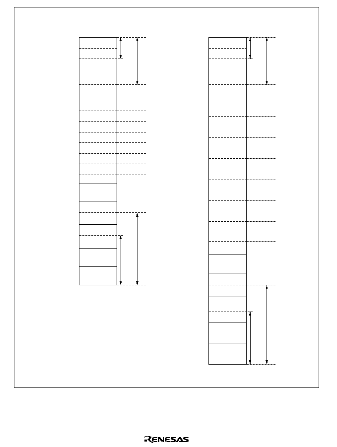
66
H'00000
H'000FF
H'07FFF
Memory-indirect
branch addresses
16-bit absolute
addresses
Modes 1 and 2
(1-Mbyte expanded modes with
on-chip ROM disabled)
H'1FFFF
H'20000
H'3FFFF
H'40000
H'5FFFF
H'60000
H'7FFFF
H'80000
H'9FFFF
H'A0000
H'BFFFF
H'C0000
H'DFFFF
H'E0000
Area 0
Area 1
Area 2
Area 3
Area 4
Area 5
Area 6
Area 7
External address
space
External address
space
Vector area
On-chip RAM
*
On-chip RAM
*
8-bit absolute addresses
16-bit absolute addresses
H'F8000
H'FBF1F
H'FBF20
H'FFF00
H'FFF1F
H'FFF20
H'FFFE9
H'FFFEA
H'FFFFF
Modes 3 and 4
(16-Mbyte expanded modes with
on-chip ROM disabled)
H'000000
H'0000FF
H'007FFF
Memory-indirect
branch addresses
16-bit absolute
addresses
H'1FFFFF
H'200000
Area 0
Area 1
Area 2
Area 3
Area 4
Area 5
Area 6
Area 7
External
address
space
Vector area
External
address
space
8-bit absolute addresses
16-bit absolute addresses
H'FF8000
H'FFBF1F
H'FFBF20
H'FFFF1F
H'FFFF20
H'FFFF00
H'FFFFE9
H'FFFFEA
H'FFFFFF
H'3FFFFF
H'400000
H'5FFFFF
H'600000
H'7FFFFF
H'800000
H'9FFFFF
H'A00000
H'BFFFFF
H'C00000
H'DFFFFF
H'E00000
H'FEE000
H'FEE0FF
Internal I/O
registers (1)
Internal I/O
registers (1)
Internal I/O
registers (2)
Internal I/O
registers (2)
External
address
space
H'EE000
H'EE0FF
External address
space
Note:
*
External addresses can be accessed by disabling on-chip RAM.
Figure 3.1(1) H8/3069F Memory Map in Each Operating Mode (EMC = 1)
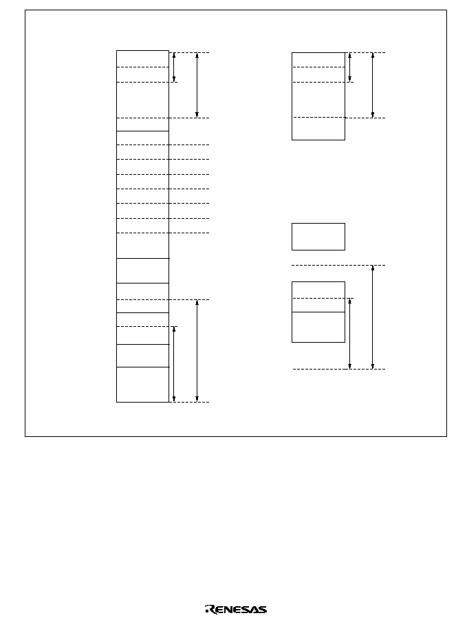
67
H'000000
H'0000FF
H'007FFF
Memory-indirect
branch addresses
16-bit absolute
addresses
Mode 5
(16-Mbyte expanded mode with
on-chip ROM enabled)
Mode 7
(single-chip advanced mode)
H'07FFFF
H'080000
H'1FFFFF
H'200000
H'3FFFFF
H'400000
H'5FFFFF
H'600000
H'7FFFFF
H'800000
H'9FFFFF
H'A00000
H'BFFFFF
H'C00000
H'DFFFFF
H'E00000
Area 0
Area 1
Area 2
Area 3
Area 4
Area 5
Area 6
Area 7
External address
space
External address
space
Vector area
On-chip ROM
On-chip RAM
*
External
address
space
Internal I/O
registers (1)
Internal I/O
registers (2)
8-bit absolute addresses
16-bit absolute addresses
H'FEE000
H'FEE0FF
H'FF8000
H'FFBF1F
H'FFBF20
H'FFFF00
H'FFFF1F
H'FFFF20
H'FFFFE9
H'FFFFEA
H'FFFFFF
H'00000
H'000FF
Memory-indirect
branch addresses
16-bit absolute
addresses
Vector area
On-chip ROM
On-chip RAM
Internal I/O
registers(2)
8-bit absolute addresses
16-bit absolute addresses
H'EE000
H'EE0FF
H'FFF1F
H'FFF20
H'FBF20
H'FFFE9
H'FFFFF
H'FFF00
H'07FFF
H'7FFFF
H'F8000
Internal I/O
registers (1)
Note:
*
External addresses can be accessed by disabling on-chip RAM.
Figure 3.1(2) H8/3069F Memory Map in Each Operating Mode (EMC = 1)
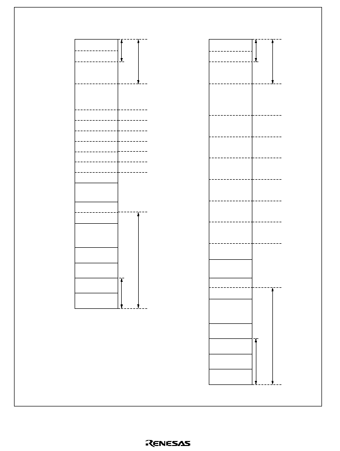
68
Vector area
Vector area
External address
space
Internal I/O
registers (1)
Internal I/O
registers (2)
External address
space
On-chip RAM
*
Internal I/O
registers (3)
External address
space
On-chip RAM
*
External address
space
Internal I/O
registers (1)
External address
space
On-chip RAM
*
Internal I/O
registers (2)
External address
space
On-chip RAM
*
Internal I/O
registers (3)
H'00000
H'000FF
H'07FFF
H'1FFFF
H'20000
H'3FFFF
H'40000
H'5FFFF
H'60000
H'7FFFF
H'80000
H'9FFFF
H'A0000
H'BFFFF
H'C0000
H'DFFFF
H'E0000
H'EE000
H'EE0FF
H'F8000
H'FBEDF
H'FBEE0
H'FFE7F
H'FFE80
H'FFEFF
H'FFF00
H'FFF7F
H'FFF80
H'FFFDF
H'FFFE0
H'FFFFF
H'000000
H'0000FF
H'007FFF
H'1FFFFF
H'200000
H'3FFFFF
H'400000
H'5FFFFF
H'600000
H'7FFFFF
H'800000
H'9FFFFF
H'A00000
H'BFFFFF
H'C00000
H'DFFFFF
H'E00000
H'FEE000
H'FEE0FF
H'FF8000
H'FFBEDF
H'FFBEE0
H'FFFE7F
H'FFFE80
H'FFFEFF
H'FFFF00
H'FFFF7F
H'FFFF80
H'FFFFDF
H'FFFFE0
H'FFFFFF
Modes 1 and 2
(1-Mbyte expanded modes with
on-chip ROM disabled)
Modes 3 and 4
(16-Mbyte expanded modes with
on-chip ROM disabled)
Memory-indirect
branch addresses
16-bit absolute
addresses
Area 0
Area 1
Area 2
Area 3
Area 4
Area 5
Area 6
Area 7
8-bit absolute
addresses
16-bit absolute addresses
Memory-indirect
branch addresses
16-bit absolute
addresses
Area 0
Area 1
Area 2
Area 3
Area 4
Area 5
Area 6
Area 7
8-bit absolute addresses
16-bit absolute addresses
Note:
*
This area becomes external address space when on-chip RAM is disabled.
Figure 3.2(1) H8/3069F Memory Map in Each Operating Mode (EMC = 0)
69
Vector area
On-chip ROM
External address
space
Internal I/O
registers (1)
Internal I/O
registers (2)
External address
space
On-chip RAM
*
Internal I/O
registers (3)
On-chip RAM
*
External address
space
Vector area
On-chip ROM
Internal I/O
registers (1)
On-chip RAM
*
Internal I/O
registers (2)
On-chip RAM
*
Internal I/O
registers (3)
H'00000
H'000FF
H'07FFF
H'EE000
H'EE0FF
H'F8000
H'FBEE0
H'FFE7F
H'FFE80
H'FFEFF
H'FFF80
H'FFFDF
H'FFFE0
H'FFFFF
H'000000
H'0000FF
H'007FFF
H'1FFFFF
H'200000
H'07FFFF
H'080000
H'7FFFF
H'3FFFFF
H'400000
H'5FFFFF
H'600000
H'7FFFFF
H'800000
H'9FFFFF
H'A00000
H'BFFFFF
H'C00000
H'DFFFFF
H'E00000
H'FEE000
H'FEE0FF
H'FF8000
H'FFBEDF
H'FFBEE0
H'FFFE7F
H'FFFE80
H'FFFEFF
H'FFFF00
H'FFFF7F
H'FFFF80
H'FFFFDF
H'FFFFE0
H'FFFFFF
Mode 5
(16-Mbyte expanded mode with
on-chip ROM enabled)
Mode 7
(single-chip advanced mode)
Memory-indirect
branch addresses
16-bit absolute
addresses
8-bit absolute
addresses
16-bit absolute addresses
Memory-indirect
branch addresses
16-bit absolute
addresses
Area 0
Area 1
Area 2
Area 3
Area 4
Area 5
Area 6
Area 7
8-bit absolute addresses
16-bit absolute addresses
Note:
*
This area becomes external address space when on-chip RAM is disabled.
Figure 3.2(2) H8/3069F Memory Map in Each Operating Mode (EMC = 0)

70

71
Section 4 Exception Handling
4.1
Overview
4.1.1
Exception Handling Types and Priority
As table 4.1 indicates, exception handling may be caused by a reset, trap instruction, or interrupt.
Exception handling is prioritized as shown in table 4.1. If two or more exceptions occur
simultaneously, they are accepted and processed in priority order. Trap instruction exceptions are
accepted at all times in the program execution state.
Table 4.1
Exception Types and Priority
Priority
Exception Type
Start of Exception Handling
High
Reset
Starts immediately after a low-to-high transition at the RES pin
Interrupt
Interrupt requests are handled when execution of the current
instruction or handling of the current exception is completed
Low
Trap instruction (TRAPA) Started by execution of a trap instruction (TRAPA)
4.1.2
Exception Handling Operation
Exceptions originate from various sources. Trap instructions and interrupts are handled as follows.
1. The program counter (PC) and condition code register (CCR) are pushed onto the stack.
2. The CCR interrupt mask bit is set to 1.
3. A vector address corresponding to the exception source is generated, and program execution
starts from that address.
Note:
For a reset exception, steps 2 and 3 above are carried out.

72
4.1.3
Exception Vector Table
The exception sources are classified as shown in figure 4.1. Different vectors are assigned to
different exception sources. Table 4.2 lists the exception sources and their vector addresses.
Exception
sources
� Reset
� Interrupts
� Trap instruction
External interrupts:
Internal interrupts:
NMI, IRQ to IRQ
36 interrupts from on-chip
supporting modules
0 5
Figure 4.1 Exception Sources

73
Table 4.2
Exception Vector Table
Vector Address
*
1
Exception Source
Vector Number
Advanced Mode
Normal Mode
*
3
Reset
0
H'0000 to H'0003
H'0000 to H'0001
Reserved for system use
1
H'0004 to H'0007
H'0002 to H'0003
2
H'0008 to H'000B
H'0004 to H'0005
3
H'000C to H'000F
H'0006 to H'0007
4
H'0010 to H'0013
H'0008 to H'0009
5
H'0014 to H'0017
H'000A to H'000B
6
H'0018 to H'001B
H'000C to H'000D
External interrupt (NMI)
7
H'001C to H'001F
H'000E to H'000F
Trap instruction (4 sources)
8
H'0020 to H'0023
H'0010 to H'0011
9
H'0024 to H'0027
H'0012 to H'0013
10
H'0028 to H'002B
H'0014 to H'0015
11
H'002C to H'002F
H'0016 to H'0017
External interrupt IRQ
0
12
H'0030 to H'0033
H'0018 to H'0019
External interrupt IRQ
1
13
H'0034 to H'0037
H'001A to H'001B
External interrupt IRQ
2
14
H'0038 to H'003B
H'001C to H'001D
External interrupt IRQ
3
15
H'003C to H'003F
H'001E to H'001F
External interrupt IRQ
4
16
H'0040 to H'0043
H'0020 to H'0021
External interrupt IRQ
5
17
H'0044 to H'0047
H'0022 to H'0023
Reserved for system use
18
H'0048 to H'004B
H'0024 to H'0025
19
H'004C to H'004F
H'0026 to H'0027
Internal interrupts
*
2
20
to
63
H'0050 to H'0053
to
H'00FC to H'00FF
H'0028 to H'0029
to
H'007E to H'007F
Notes:
*
1 Lower 16 bits of the address.
*
2 For the internal interrupt vectors, see section 5.3.3, Interrupt Vector Table.
*
3 Cannot be selected in H8/3069F.

74
4.2
Reset
4.2.1
Overview
A reset is the highest-priority exception. When the
RES pin goes low, all processing halts and the
chip enters the reset state. A reset initializes the internal state of the CPU and the registers of the
on-chip supporting modules. Reset exception handling begins when the
RES pin changes from
low to high.
The chip can also be reset by overflow of the watchdog timer. For details see section 12,
Watchdog Timer.
4.2.2
Reset Sequence
The chip enters the reset state when the
RES pin goes low.
To ensure that the chip is reset, hold the
RES pin low for at least 20 ms at power-up. To reset the
chip during operation, hold the
RES pin low for at least 20 system clock (
) cycles. See appendix
D.2, Pin States at Reset, for the states of the pins in the reset state.
When the
RES pin goes high after being held low for the necessary time, the chip starts reset
exception handling as follows.
�
The internal state of the CPU and the registers of the on-chip supporting modules are
initialized, and the I bit is set to 1 in CCR.
�
The contents of the reset vector address (H'0000 to H'0003 in advanced mode, H'0000 to
H'0001 in normal mode) are read, and program execution starts from the address indicated in
the vector address.
Note : The normal mode cannot be selected in the H8/3069F
Figure 4.2 shows the reset sequence in modes 1 and 3. Figure 4.3 shows the reset sequence in
modes 2 and 4.
�
After power is turned on, hold the
RES pin low and the STBY pin high.
75
Address
bu
s
RES
RD
HWR
D to D
15
8
V
ector f
etch
Inter
nal
processing
Pref
etch of
first prog
r
a
m
instr
uction
(1), (3), (5), (7)
(2), (4), (6), (8)
(9)
(10)
Note:
After a reset, the w
ait-state controller inser
ts three w
ait states in e
v
er
y b
us cycle
.
Address of reset v
ector
:
(1) = H'000000, (3) = H'000001, (5) = H'000002, (7) = H'000003
Star
t address (contents of reset e
xception handling v
ector address)
Star
t address
First instr
uction of prog
r
a
m
High
(1)
(3)
(5)
(7)
(9)
(2)
(4)
(6)
(8)
(10)
LW
R
,
Figure 4.2 Reset Sequence (Modes 1 and 3)
76
Address bus
RES
RD
HWR
D to D
15
0
Vector fetch
Internal
processing
Prefetch of first
program instruction
(1), (3)
(2), (4)
(5)
(6)
Note: After a reset, the wait-state controller inserts three wait states in every bus cycle.
High
LWR
,
Address of reset vector: (1) = H'000000, (3) = H'000002
Start address (contents of reset exception handling vector address)
Start address
First instruction of program
(2)
(4)
(3)
(1)
(5)
(6)
Figure 4.3 Reset Sequence (Modes 2 and 4)
4.2.3
Interrupts after Reset
If an interrupt is accepted after a reset but before the stack pointer (SP) is initialized, PC and CCR
will not be saved correctly, leading to a program crash. To prevent this, all interrupt requests,
including NMI, are disabled immediately after a reset. The first instruction of the program is
always executed immediately after the reset state ends. This instruction should initialize the stack
pointer (example: MOV.L #xx:32, SP).

77
4.3
Interrupts
Interrupt exception handling can be requested by seven external sources (NMI, IRQ
0
to IRQ
5
), and
36 internal sources in the on-chip supporting modules. Figure 4.4 classifies the interrupt sources
and indicates the number of interrupts of each type.
The on-chip supporting modules that can request interrupts are the watchdog timer (WDT),
DRAM interface, 16-bit timer, 8-bit timer, DMA controller (DMAC), serial communication
interface (SCI), and A/D converter. Each interrupt source has a separate vector address.
NMI is the highest-priority interrupt and is always accepted*. Interrupts are controlled by the
interrupt controller. The interrupt controller can assign interrupts other than NMI to two priority
levels, and arbitrate between simultaneous interrupts. Interrupt priorities are assigned in interrupt
priority registers A and B (IPRA and IPRB) in the interrupt controller.
Note: * NMI input is sometimes disabled when flash memory is being programmed or erased. For
details see section 18.4.5 Flash Vector Address Control Register (FVACR).
For details on interrupts see section 5, Interrupt Controller.
Interrupts
External interrupts
Internal interrupts
NMI (1)
IRQ to IRQ (6)
WDT
*
1
(1)
DRAM interface
*
2
(1)
16-bit timer (9)
8-bit timer (8)
DMAC (4)
SCI (12)
A/D converter (1)
0 5
Notes: Numbers in parentheses are the number of interrupt sources.
*
1 When the watchdog timer is used as an interval timer, it generates an interrupt request
at every counter overflow.
*
2 When the DRAM interface is used as an interval timer, it generates an interrupt request
at compare match.
Figure 4.4 Interrupt Sources and Number of Interrupts

78
4.4
Trap Instruction
Trap instruction exception handling starts when a TRAPA instruction is executed. If the UE bit is
set to 1 in the system control register (SYSCR), the exception handling sequence sets the I bit to 1
in CCR. If the UE bit is 0, the I and UI bits are both set to 1. The TRAPA instruction fetches a
start address from a vector table entry corresponding to a vector number from 0 to 3, which is
specified in the instruction code.
79
4.5
Stack Status after Exception Handling
Figure 4.5 shows the stack after completion of trap instruction exception handling and interrupt
exception handling.
SP�4
SP�3
SP�2
SP�1
SP (ER7)
SP (ER7)
SP+1
SP+2
SP+3
SP+4
SP�4
SP�3
SP�2
SP�1
SP (ER7)
SP (ER7)
SP+1
SP+2
SP+3
SP+4
Before exception handling
Before exception handling
After exception handling
Stack area
Stack area
CCR
CCR
PC
PC
CCR
PC
PC
PC
H
L
E
H
L
*
2
After exception handling
Even address
Even address
Pushed on stack
Pushed on stack
a. Normal mode
*
1
b. Advanced mode
Legend
PCE:
PCH:
PCL:
CCR:
SP:
Notes:
PC indicates the address of the first instruction that will be executed after return.
Registers must be saved in word or longword size at even addresses.
Ignored at return.
1.
2.
*
2
Cannot be selected in H8/3069F
*
1
Bits 23 to 16 of program counter (PC)
Bits 15 to 8 of program counter (PC)
Bits 7 to 0 of program counter (PC)
Condition code register
Stack pointer
Figure 4.5 Stack after Completion of Exception Handling

80
4.6
Notes on Stack Usage
When accessing word data or longword data, the H8/3069F regards the lowest address bit as 0.
The stack should always be accessed by word access or longword access, and the value of the
stack pointer (SP, ER7) should always be kept even.
Use the following instructions to save registers:
PUSH.W Rn
(or MOV.W Rn, @�SP)
PUSH.L ERn
(or MOV.L ERn, @�SP)
Use the following instructions to restore registers:
POP.W Rn
(or MOV.W @SP+, Rn)
POP.L ERn
(or MOV.L @SP+, ERn)
Setting SP to an odd value may lead to a malfunction. Figure 4.6 shows an example of what
happens when the SP value is odd.
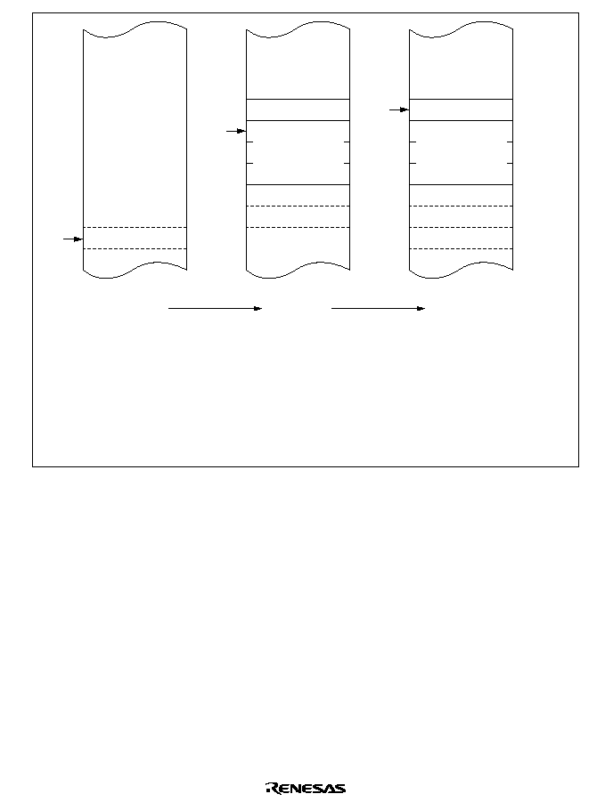
81
TRAPA instruction executed
CCR
Legend
CCR:
PC:
R1L:
SP:
SP
PC
R1L
PC
SP
SP
MOV. B R1L, @-ER7
SP set to H'FFFEFF
Data saved above SP
CCR contents lost
Condition code register
Program counter
General register R1L
Stack pointer
Note: The diagram illustrates modes 3 and 4.
H'FFFEFA
H'FFFEFB
H'FFFEFC
H'FFFEFD
H'FFFEFF
Figure 4.6 Operation when SP Value is Odd

82

83
Section 5 Interrupt Controller
5.1
Overview
5.1.1
Features
The interrupt controller has the following features:
�
Interrupt priority registers (IPRs) for setting interrupt priorities
Interrupts other than NMI can be assigned to two priority levels on a module-by-module basis
in interrupt priority registers A and B (IPRA and IPRB).
�
Three-level masking by the I and UI bits in the CPU condition code register (CCR)
�
Seven external interrupt pins
NMI has the highest priority and is always accepted*; either the rising or falling edge can be
selected. For each of IRQ
0
to IRQ
5
, sensing of the falling edge or level sensing can be selected
independently.
Note: * NMI input is sometimes disabled when flash memory is being programmed or erased. For
details see section 18.4.5 Flash Vector Address Control Register (FVACR).
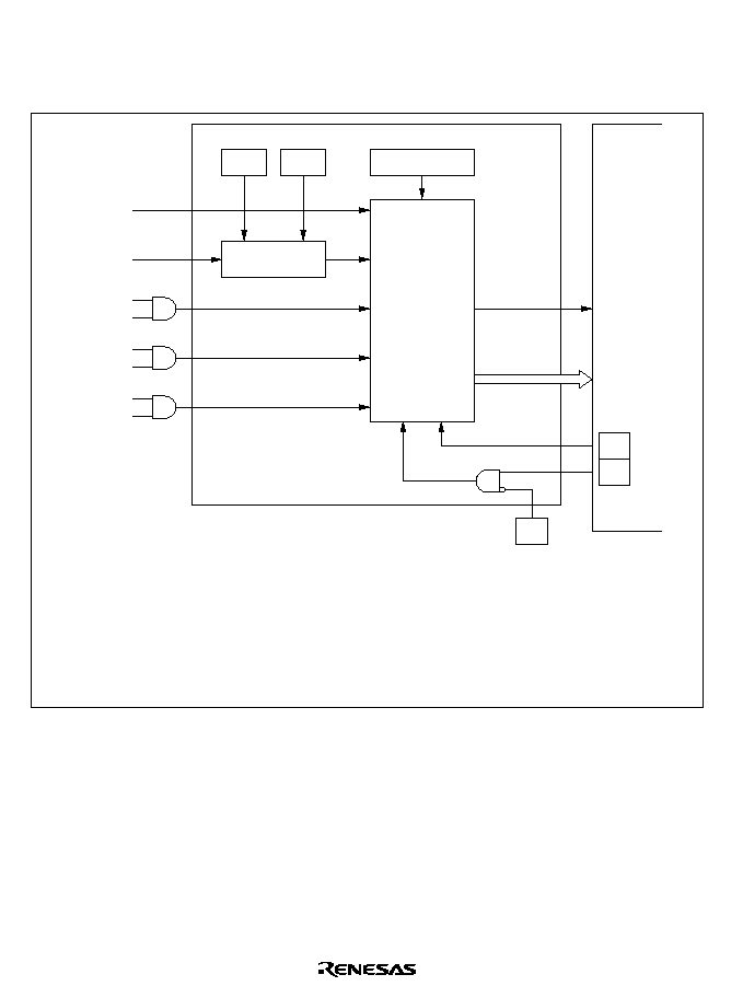
84
5.1.2
Block Diagram
Figure 5.1 shows a block diagram of the interrupt controller.
ISCR
IER
IPRA, IPRB
.
.
.
OVF
TME
TEI
TEIE
.
.
.
.
.
.
.
CPU
CCR
I
UI
UE
SYSCR
ISCR:
IER:
ISR:
IPRA:
IPRB:
SYSCR:
NMI
input
IRQ input
IRQ input
section ISR
Interrupt controller
Priority
decision logic
Interrupt
request
Vector
number
IRQ sense control register
IRQ enable register
IRQ status register
Interrupt priority register A
Interrupt priority register B
System control register
Legend
Figure 5.1 Interrupt Controller Block Diagram

85
5.1.3
Pin Configuration
Table 5.1 lists the interrupt pins.
Table 5.1
Interrupt Pins
Name
Abbreviation I/O
Function
Nonmaskable interrupt
NMI
Input
Nonmaskable interrupt
*
, rising edge or
falling edge selectable
External interrupt request 5 to 0
IRQ
5
to
IRQ
0
Input
Maskable interrupts, falling edge or level
sensing selectable
Note:
*
NMI input is sometimes disabled when flash memory is being programmed or erased. For
details see section 18.4.5, Flash Vector Address Control Register (FVACR).
5.1.4
Register Configuration
Table 5.2 lists the registers of the interrupt controller.
Table 5.2
Interrupt Controller Registers
Address
*
1
Name
Abbreviation
R/W
Initial Value
H'EE012
System control register
SYSCR
R/W
H'09
H'EE014
IRQ sense control register
ISCR
R/W
H'00
H'EE015
IRQ enable register
IER
R/W
H'00
H'EE016
IRQ status register
ISR
R/(W)
*
2
H'00
H'EE018
Interrupt priority register A
IPRA
R/W
H'00
H'EE019
Interrupt priority register B
IPRB
R/W
H'00
Notes:
*
1 Lower 20 bits of the address in advanced mode.
*
2 Only 0 can be written, to clear flags.
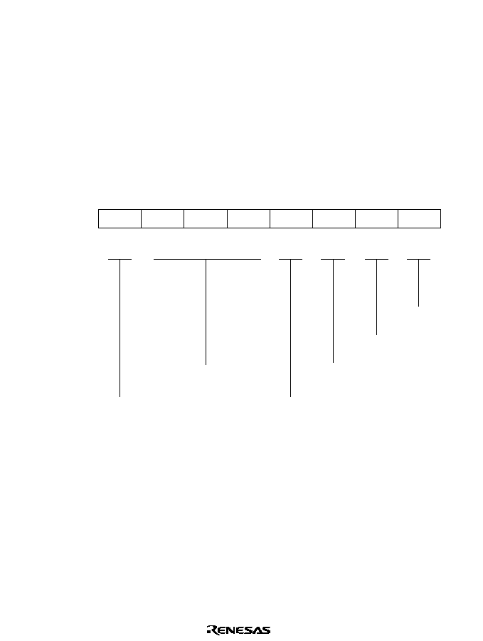
86
5.2
Register Descriptions
5.2.1
System Control Register (SYSCR)
SYSCR is an 8-bit readable/writable register that controls software standby mode, selects the
action of the UI bit in CCR, selects the NMI edge, and enables or disables the on-chip RAM.
Only bits 3 and 2 are described here. For the other bits, see section 3.3, System Control Register
(SYSCR).
SYSCR is initialized to H'09 by a reset and in hardware standby mode. It is not initialized in
software standby mode.
Bit
Initial value
Read/Write
7
SSBY
0
R/W
6
STS2
0
R/W
5
STS1
0
R/W
4
STS0
0
R/W
3
UE
1
R/W
0
RAME
1
R/W
2
NMIEG
0
R/W
1
SSOE
0
R/W
Software standby
Standby timer
select 2 to 0
User bit enable
Selects whether to use the UI bit in
CCR as a user bit or interrupt mask bit
NMI edge select
Selects the NMI input edge
Software standby
output port enable
RAM enable

87
Bit 3--User Bit Enable (UE): Selects whether to use the UI bit in CCR as a user bit or an
interrupt mask bit.
Bit 3
UE
Description
0
UI bit in CCR is used as interrupt mask bit
1
UI bit in CCR is used as user bit
(Initial value)
Bit 2--NMI Edge Select (NMIEG): Selects the NMI input edge.
Bit 2
NMIEG
Description
0
Interrupt is requested at falling edge of NMI input
(Initial value)
1
Interrupt is requested at rising edge of NMI input
5.2.2
Interrupt Priority Registers A and B (IPRA, IPRB)
IPRA and IPRB are 8-bit readable/writable registers that control interrupt priority.

88
Interrupt Priority Register A (IPRA): IPRA is an 8-bit readable/writable register in which
interrupt priority levels can be set.
Bit
Initial value
Read/Write
7
IPRA7
0
R/W
6
IPRA6
0
R/W
5
IPRA5
0
R/W
4
IPRA4
0
R/W
3
IPRA3
0
R/W
0
IPRA0
0
R/W
2
IPRA2
0
R/W
1
IPRA1
0
R/W
Priority level A7
Selects the priority level of IRQ interrupt requests
Priority level A3
Selects the priority level of WDT,
DRAM interface, and A/D converter
interrupt requests
Priority level A2
Selects the priority level of
16-bit timer channel 0 interrupt
requests
Priority level A1
Selects the priority level
of 16-bit timer channel 1
interrupt requests
Priority
level A0
Selects the
priority level
of 16-bit timer
channel 2
interrupt
requests
Selects the priority level of IRQ interrupt requests
Priority level A6
Selects the priority level of IRQ and IRQ interrupt requests
Priority level A5
Selects the priority level of IRQ and IRQ
interrupt requests
Priority level A4
0
1
2
3
4
5
IPRA is initialized to H'00 by a reset and in hardware standby mode.

89
Bit 7--Priority Level A7 (IPRA7): Selects the priority level of IRQ
0
interrupt requests.
Bit 7
IPRA7
Description
0
IRQ
0
interrupt requests have priority level 0 (low priority)
(Initial value)
1
IRQ
0
interrupt requests have priority level 1 (high priority)
Bit 6--Priority Level A6 (IPRA6): Selects the priority level of IRQ
1
interrupt requests.
Bit 6
IPRA6
Description
0
IRQ
1
interrupt requests have priority level 0 (low priority)
(Initial value)
1
IRQ
1
interrupt requests have priority level 1 (high priority)
Bit 5--Priority Level A5 (IPRA5): Selects the priority level of IRQ
2
and IRQ
3
interrupt requests.
Bit 5
IPRA5
Description
0
IRQ
2
and IRQ
3
interrupt requests have priority level 0 (low priority)
(Initial value)
1
IRQ
2
and IRQ
3
interrupt requests have priority level 1 (high priority)
Bit 4--Priority Level A4 (IPRA4): Selects the priority level of IRQ
4
and IRQ
5
interrupt requests.
Bit 4
IPRA4
Description
0
IRQ
4
and IRQ
5
interrupt requests have priority level 0 (low priority)
(Initial value)
1
IRQ
4
and IRQ
5
interrupt requests have priority level 1 (high priority)

90
Bit 3--Priority Level A3 (IPRA3): Selects the priority level of WDT, DRAM interface, and A/D
converter interrupt requests.
Bit 3
IPRA3
Description
0
WDT, DRAM interface, and A/D converter interrupt requests have priority level 0
(low priority)
(Initial value)
1
WDT, DRAM interface, and A/D converter interrupt requests have priority level 1
(high priority)
Bit 2--Priority Level A2 (IPRA2): Selects the priority level of 16-bit timer channel 0 interrupt
requests.
Bit 2
IPRA2
Description
0
16-bit timer channel 0 interrupt requests have priority level 0 (low priority) (Initial value)
1
16-bit timer channel 0 interrupt requests have priority level 1 (high priority)
Bit 1--Priority Level A1 (IPRA1): Selects the priority level of 16-bit timer channel 1 interrupt
requests.
Bit 1
IPRA1
Description
0
16-bit timer channel 1 interrupt requests have priority level 0 (low priority) (Initial value)
1
16-bit timer channel 1 interrupt requests have priority level 1 (high priority)
Bit 0--Priority Level A0 (IPRA0): Selects the priority level of 16-bit timer channel 2 interrupt
requests.
Bit 0
IPRA0
Description
0
16-bit timer channel 2 interrupt requests have priority level 0 (low priority) (Initial value)
1
16-bit timer channel 2 interrupt requests have priority level 1 (high priority)

91
Interrupt Priority Register B (IPRB): IPRB is an 8-bit readable/writable register in which
interrupt priority levels can be set.
Bit
Initial value
Read/Write
7
IPRB7
0
R/W
6
IPRB6
0
R/W
5
IPRB5
0
R/W
4
--
0
R/W
3
IPRB3
0
R/W
0
--
0
R/W
2
IPRB2
0
R/W
1
IPRB1
0
R/W
Priority level B7
Selects the priority level of 8-bit timer channel 0, 1 interrupt requests
Priority level B3
Selects the priority level of SCI
channel 0 interrupt requests
Priority level B2
Selects the priority level of
SCI channel 1 interrupt requests
Priority level B1
Selects the priority level
of SCI channel 2 interrupt
requests
Reserved bit
Selects the priority level of 8-bit timer channel 2, 3 interrupt requests
Priority level B6
Selects the priority level of DMAC
interrupt requests (channels 0 and 1)
Priority level B5
Reserved bit
IPRB is initialized to H'00 by a reset and in hardware standby mode.

92
Bit 7--Priority Level B7 (IPRB7): Selects the priority level of 8-bit timer channel 0, 1 interrupt
requests.
Bit 7
IPRB7
Description
0
8-bit timer channel 0, 1 interrupt requests have priority level 0 (low priority)(Initial value)
1
8-bit timer channel 0, 1 interrupt requests have priority level 1 (high priority)
Bit 6--Priority Level B6 (IPRB6): Selects the priority level of 8-bit timer channel 2, 3 interrupt
requests.
Bit 6
IPRB6
Description
0
8-bit timer channel 2, 3 interrupt requests have priority level 0 (low priority)(Initial value)
1
8-bit timer channel 2, 3 interrupt requests have priority level 1 (high priority)
Bit 5--Priority Level B5 (IPRB5): Selects the priority level of DMAC interrupt requests
(channels 0 and 1).
Bit 5
IPRB5
Description
0
DMAC interrupt requests (channels 0 and 1) have priority level 0
(Initial value)
(low priority)
1
DMAC interrupt requests (channels 0 and 1) have priority level 1 (high priority)
Bit 4--Reserved: This bit can be written and read, but it does not affect interrupt priority.

93
Bit 3--Priority Level B3 (IPRB3): Selects the priority level of SCI channel 0 interrupt requests.
Bit 3
IPRB3
Description
0
SCI0 interrupt requests have priority level 0 (low priority)
(Initial value)
1
SCI0 interrupt requests have priority level 1 (high priority)
Bit 2--Priority Level B2 (IPRB2): Selects the priority level of SCI channel 1 interrupt requests.
Bit 2
IPRB2
Description
0
SCI1 interrupt requests have priority level 0 (low priority)
(Initial value)
1
SCI1 interrupt requests have priority level 1 (high priority)
Bit 1--Priority Level B1 (IPRB1): Selects the priority level of SCI channel 2 interrupt requests.
Bit 1
IPRB1
Description
0
SCI channel 2 interrupt requests have priority level 0 (low priority)
(Initial value)
1
SCI channel 2 interrupt requests have priority level 1 (high priority)
Bit 0--Reserved: This bit can be written and read, but it does not affect interrupt priority.

94
5.2.3
IRQ Status Register (ISR)
ISR is an 8-bit readable/writable register that indicates the status of IRQ
0
to IRQ
5
interrupt
requests.
Bit
Initial value
Read/Write
7
--
0
--
These bits indicate IRQ to IRQ
interrupt request status
Note: Only 0 can be written, to clear flags.
*
6
--
0
--
5
IRQ5F
0
R/(W)
*
4
IRQ4F
0
R/(W)
*
3
IRQ3F
0
R/(W)
*
2
IRQ2F
0
R/(W)
*
1
IRQ1F
0
R/(W)
*
0
IRQ0F
0
R/(W)
*
5
0
IRQ to IRQ flags
5
0
Reserved bits
ISR is initialized to H'00 by a reset and in hardware standby mode.
Bits 7 and 6--Reserved: These bits can not be modified and are always read as 0.
Bits 5 to 0--IRQ
5
to IRQ
0
Flags (IRQ5F to IRQ0F): These bits indicate the status of IRQ
5
to
IRQ
0
interrupt requests.
Bits 5 to 0
IRQ5F to IRQ0F Description
0
[Clearing conditions]
(Initial value)
0 is written in IRQnF after reading the IRQnF flag when IRQnF = 1.
IRQnSC = 0,
IRQn
input is high, and interrupt exception handling is carried out.
IRQnSC = 1 and IRQn interrupt exception handling is carried out.
1
[Setting conditions]
IRQnSC = 0 and
IRQn
input is low.
IRQnSC = 1 and
IRQn
input changes from high to low.
Note: n = 5 to 0

95
5.2.4
IRQ Enable Register (IER)
IER is an 8-bit readable/writable register that enables or disables IRQ
5
to IRQ
0
interrupt requests.
Bit
Initial value
Read/Write
7
--
0
R/W
These bits enable or disable IRQ to IRQ interrupts
6
--
0
R/W
5
IRQ5E
0
R/W
4
IRQ4E
0
R/W
3
IRQ3E
0
R/W
2
IRQ2E
0
R/W
1
IRQ1E
0
R/W
0
IRQ0E
0
R/W
5
0
IRQ to IRQ enable
5
0
Reserved bits
IER is initialized to H'00 by a reset and in hardware standby mode.
Bits 7 and 6--Reserved: These bits can be written and read, but they do not enable or disable
interrupts.
Bits 5 to 0--IRQ
5
to IRQ
0
Enable (IRQ5E to IRQ0E): These bits enable or disable
IRQ
5
to IRQ
0
interrupts.
Bits 5 to 0
IRQ5E to IRQ0E Description
0
IRQ
5
to IRQ
0
interrupts are disabled
(Initial value)
1
IRQ
5
to IRQ
0
interrupts are enabled

96
5.2.5
IRQ Sense Control Register (ISCR)
ISCR is an 8-bit readable/writable register that selects level sensing or falling-edge sensing of the
inputs at pins
IRQ
5
to
IRQ
0
.
Bit
Initial value
Read/Write
7
--
0
R/W
These bits select level sensing or falling-edge
sensing for IRQ to IRQ interrupts
6
--
0
R/W
5
IRQ5SC
0
R/W
4
IRQ4SC
0
R/W
3
IRQ3SC
0
R/W
2
IRQ2SC
0
R/W
1
IRQ1SC
0
R/W
0
IRQ0SC
0
R/W
5
0
IRQ to IRQ sense control
5
0
Reserved bits
ISCR is initialized to H'00 by a reset and in hardware standby mode.
Bits 7 and 6--Reserved: These bits can be written and read, but they do not select level or
falling-edge sensing.
Bits 5 to 0--IRQ
5
to IRQ
0
Sense Control (IRQ5SC to IRQ0SC): These bits select whether
interrupts IRQ
5
to IRQ
0
are requested by level sensing of pins
IRQ
5
to
IRQ
0
, or by falling-edge
sensing.
Bits 5 to 0
IRQ5SC to IRQ0SC Description
0
Interrupts are requested when
IRQ
5
to
IRQ
0
inputs are low
(Initial value)
1
Interrupts are requested by falling-edge input at
IRQ
5
to
IRQ
0
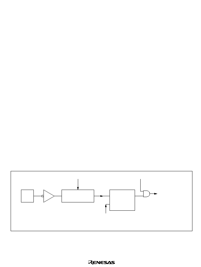
97
5.3
Interrupt Sources
The interrupt sources include external interrupts (NMI, IRQ
0
to IRQ
5
) and 36 internal interrupts.
5.3.1
External Interrupts
There are seven external interrupts: NMI and IRQ
0
to IRQ
5
. Of these, NMI, IRQ
0
, IRQ
1
, and IRQ
2
can be used to exit software standby mode.
NMI: NMI is the highest-priority interrupt and is always accepted, regardless of the states of the I
and UI bits in CCR*. The NMIEG bit in SYSCR selects whether an interrupt is requested by the
rising or falling edge of the input at the NMI pin. NMI interrupt exception handling has vector
number 7.
Note: * NMI input is sometimes disabled when flash memory is being programmed or erased. For
details see section 18.4.5, Flash Vector Address Control Register (FVACR).
IRQ
0
to IRQ
5
Interrupts: These interrupts are requested by input signals at pins
IRQ
0
to
IRQ
5
.
The IRQ
0
to IRQ
5
interrupts have the following features.
�
ISCR settings can select whether an interrupt is requested by the low level of the input at pins
IRQ
0
to
IRQ
5
, or by the falling edge.
�
IER settings can enable or disable the IRQ
0
to IRQ
5
interrupts. Interrupt priority levels can be
assigned by four bits in IPRA (IPRA7 to IPRA4).
�
The status of IRQ
0
to IRQ
5
interrupt requests is indicated in ISR. The ISR flags can be cleared
to 0 by software.
Figure 5.2 shows a block diagram of interrupts IRQ
0
to IRQ
5
.
input
Edge/level
sense circuit
IRQnSC
IRQnF
S
R
Q
IRQnE
IRQn interrupt
request
Clear signal
IRQn
Note: n = 5 to 0
Figure 5.2 Block Diagram of Interrupts IRQ
0
to IRQ
5
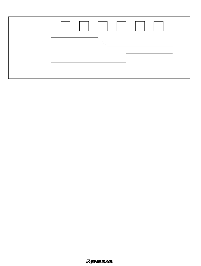
98
Figure 5.3 shows the timing of the setting of the interrupt flags (IRQnF).
IRQn
IRQnF
Note: n = 5 to 0
input pin
Figure 5.3 Timing of Setting of IRQnF
Interrupts IRQ
0
to IRQ
5
have vector numbers 12 to 17. These interrupts are detected regardless of
whether the corresponding pin is set for input or output. When using a pin for external interrupt
input, clear its DDR bit to 0 and do not use the pin for chip select output, refresh output, SCI
input/output, or A/D external trigger input.
5.3.2
Internal Interrupts
Thirty-Six internal interrupts are requested from the on-chip supporting modules.
�
Each on-chip supporting module has status flags for indicating interrupt status, and enable bits
for enabling or disabling interrupts.
�
Interrupt priority levels can be assigned in IPRA and IPRB.
�
16-bit timer, SCI, and A/D converter interrupt requests can activate the DMAC, in which case
no interrupt request is sent to the interrupt controller, and the I and UI bits are disregarded.
5.3.3
Interrupt Vector Table
Table 5.3 lists the interrupt sources, their vector addresses, and their default priority order. In the
default priority order, smaller vector numbers have higher priority. The priority of interrupts other
than NMI can be changed in IPRA and IPRB. The priority order after a reset is the default order
shown in table 5.3.

99
Table 5.3
Interrupt Sources, Vector Addresses, and Priority
Vector
Vector Address
*
1
Interrupt Source
Origin
Number Advanced Mode
Normal Mode
*
2
IPR
Priority
NMI
External
7
H'001C to H'001F H'000E to H'000F --
High
IRQ
0
pins
12
H'0030 to H'0033
H'0018 to H'0019
IPRA7
IRQ
1
13
H'0034 to H0037
H'001A to H'001B IPRA6
IRQ
2
IRQ
3
14
15
H'0038 to H'003B
H'003C to H'003F
H'001C to H'001D
H'001E to H'001F
IPRA5
IRQ
4
IRQ
5
16
17
H'0040 to H'0043
H'0044 to H'0047
H'0020 to H'0021
H'0022 to H'0023
IPRA4
Reserved
--
18
19
H'0048 to H'004B
H'004C to H'004F
H'0024 to H'0025
H'0026 to H'0027
WOVI
(interval timer)
Watchdog
timer
20
H'0050 to H'0053
H'0028 to H'0029
IPRA3
CMI
(compare match)
DRAM
interface
21
H'0054 to H'0057
H'002A to H'002B
Reserved
--
22
H'0058 to H'005B H'002C to H'002D
ADI (A/D end)
A/D
23
H'005C to H'005F H'002E to H'002F
IMIA0
(compare match/
input capture A0)
IMIB0
(compare match/
input capture B0)
OVI0 (overflow 0)
16-bit timer
channel 0
24
25
26
H'0060 to H'0063
H'0064 to H'0067
H'0068 to H'006B
H'0030 to H'0031
H'0032 to H'0033
H'0034 to H'0035
IPRA2
Reserved
--
27
H'006C to H'006F H'0036 to H'0037
IMIA1
(compare match/
inputcapture A1)
IMIB1
(compare match/
input capture B1)
OVI1 (overflow 1)
16-bit timer
channel 1
28
29
30
H'0070 to H'0073
H'0074 to H'0077
H'0078 to H'007B
H'0038 to H'0039
H'003A to H'003B
H'003C to H'003D
IPRA1
Reserved
--
31
H'007C to H'007F H'003E to H'003F
Low
Notes:
*
1
*
2
Lower 16 bits of the address.
Cannot be selected in H8/3069F.

100
Vector
Vector Address
*
1
Interrupt Source
Origin
Number Advanced Mode
Normal Mode
*
2
IPR
Priority
IMIA2
(compare match/
input capture A2)
IMIB2
(compare match/
input capture B2)
OVI2 (overflow 2)
16-bit timer
channel 2
32
33
34
H'0080 to H'0083
H'0084 to H'0087
H'0088 to H'008B
H'0040 to H'0041
H'0042 to H'0043
H'0044 to H'0045
IPRA0
High
Reserved
--
35
H'008C to H'008F H'0046 to H'0047
CMIA0
(compare match
A0)
CMIB0
(compare match
B0)
CMIA1/CMIB1
(compare match
A1/B1)
TOVI0/TOVI1
(overflow 0/1)
8-bit timer
channel 0/1
36
37
38
39
H'0090 to H'0093
H'0094 to H'0097
H'0098 to H'009B
H'009C to H'009F
H'0048 to H'0049
H'004A to H'004B
H'004C to H'004D
H'004E to H'004F
IPRB7
CMIA2
(compare match
A2)
CMIB2
(compare match
B2)
CMIA3/CMIB3
(compare match
A3/B3)
TOVI2/TOVI3
(overflow 2/3)
8-bit timer
channel 2/3
40
41
42
43
H'00A0 to H'00A3
H'00A4 to H'00A7
H'00A8 to H'00AB
H'00AC to H'00AF
H'0050 to H'0051
H'0052 to H'0053
H'0054 to H'0055
H'0056 to H'0057
IPRB6
DEND0A
DEND0B
DEND1A
DEND1B
DMAC
44
45
46
47
H'00B0 to H'00B3
H'00B4 to H'00B7
H'00B8 to H'00BB
H'00BC to H'00BF
H'0058 to H'0059
H'005A to H'005B
H'005C to H'005D
H'005E to H'005F
IPRB5
Reserved
--
48
49
50
51
H'00C0 to H'00C3
H'00C4 to H'00C7
H'00C8 to H'00CB
H'00CC to H'00CF
H'0060 to H'0061
H'0062 to H'0063
H'0064 to H'0065
H'0066 to H'0067
--
Low
Notes:
*
1
*
2
Lower 16 bits of the address.
Cannot be selected in H8/3069F.

101
Vector
Vector Address
*
1
Interrupt Source
Origin
Number Advanced Mode
Normal Mode
*
2
IPR
Priority
ERI0
(receive error 0)
RXI0 (receive
data full 0)
TXI0 (transmit
data empty 0)
TEI0
(transmit end 0)
SCI
channel 0
52
53
54
55
H'00D0 to H'00D3
H'00D4 to H'00D7
H'00D8 to H'00DB
H'00DC to H'00DF
H'0068 to H'0069
H'006A to H'006B
H'006C to H'006D
H'006E to H'006F
IPRB3
High
ERI1
(receive error 1)
RXI1 (receive
data full 1)
TXI1 (transmit
data empty 1)
TEI1 (transmit
end 1)
SCI
channel 1
56
57
58
59
H'00E0 to H'00E3
H'00E4 to H'00E7
H'00E8 to H'00EB
H'00EC to H'00EF
H'0070 to H'0071
H'0072 to H'0073
H'0074 to H'0075
H'0076 to H'0077
IPRB2
ERI2
(receive error 2)
RXI2 (receive
data full 2)
TXI2 (transmit
data empty 2)
TEI2 (transmit
end 2)
SCI
channel 2
60
61
62
63
H'00F0 to H'00F3
H'00F4 to H'00F7
H'00F8 to H'00FB
H'00FC to H'00FF
H'0078 to H'0079
H'007A to H'007B
H'007C to H'007D
H'007E to H'007F
IPRB1
Low
Notes:
*
1
*
2
Lower 16 bits of the address.
Cannot be selected in H8/3069F.

102
5.4
Interrupt Operation
5.4.1
Interrupt Handling Process
The H8/3069F handles interrupts differently depending on the setting of the UE bit. When UE = 1,
interrupts are controlled by the I bit. When UE = 0, interrupts are controlled by the I and UI bits.
Table 5.4 indicates how interrupts are handled for all setting combinations of the UE, I, and UI
bits.
NMI interrupts are always accepted except in the reset and hardware standby states*. IRQ
interrupts and interrupts from the on-chip supporting modules have their own enable bits. Interrupt
requests are ignored when the enable bits are cleared to 0.
Note: * NMI input is sometimes disabled. For details see section 18.4.5, Flash Vector Address
Control Register (FVACR).
Table 5.4
UE, I, and UI Bit Settings and Interrupt Handling
SYSCR
CCR
UE
I
UI
Description
1
0
--
All interrupts are accepted. Interrupts with priority level 1 have higher
priority.
1
--
No interrupts are accepted except NMI.
0
0
--
All interrupts are accepted. Interrupts with priority level 1 have higher
priority.
1
0
NMI and interrupts with priority level 1 are accepted.
1
No interrupts are accepted except NMI.
UE = 1: Interrupts IRQ
0
to IRQ
5
and interrupts from the on-chip supporting modules can all be
masked by the I bit in the CPU's CCR. Interrupts are masked when the I bit is set to 1, and
unmasked when the I bit is cleared to 0. Interrupts with priority level 1 have higher priority. Figure
5.4 is a flowchart showing how interrupts are accepted when UE = 1.
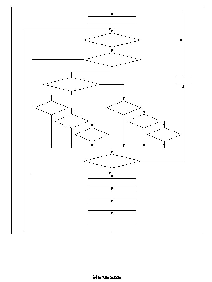
103
Program execution state
Interrupt requested?
NMI
No
Yes
No
Yes
No
Priority level 1?
No
IRQ
0
Yes
No
IRQ
1
Yes
TEI2
Yes
No
IRQ
0
Yes
No
IRQ
1
Yes
TEI2
Yes
No
I = 0
Yes
Save PC and CCR
I 1
Branch to interrupt
service routine
Pending
Yes
Read vector address
Figure 5.4 Process Up to Interrupt Acceptance when UE = 1

104
�
If an interrupt condition occurs and the corresponding interrupt enable bit is set to 1, an
interrupt request is sent to the interrupt controller.
�
When the interrupt controller receives one or more interrupt requests, it selects the highest-
priority request, following the IPR interrupt priority settings, and holds other requests pending.
If two or more interrupts with the same IPR setting are requested simultaneously, the interrupt
controller follows the priority order shown in table 5.3.
�
The interrupt controller checks the I bit. If the I bit is cleared to 0, the selected interrupt request
is accepted. If the I bit is set to 1, only NMI is accepted; other interrupt requests are held
pending.
�
When an interrupt request is accepted, interrupt exception handling starts after execution of the
current instruction has been completed.
�
In interrupt exception handling, PC and CCR are saved to the stack area. The PC value that is
saved indicates the address of the first instruction that will be executed after the return from the
interrupt service routine.
�
Next the I bit is set to 1 in CCR, masking all interrupts except NMI.
�
The vector address of the accepted interrupt is generated, and the interrupt service routine
starts executing from the address indicated by the contents of the vector address.
UE = 0: The I and UI bits in the CPU's CCR and the IPR bits enable three-level masking of
IRQ
0
to IRQ
5
interrupts and interrupts from the on-chip supporting modules.
�
Interrupt requests with priority level 0 are masked when the I bit is set to 1, and are unmasked
when the I bit is cleared to 0.
�
Interrupt requests with priority level 1 are masked when the I and UI bits are both set to 1, and
are unmasked when either the I bit or the UI bit is cleared to 0.
For example, if the interrupt enable bits of all interrupt requests are set to 1, IPRA is set to
H'20, and IPRB is set to H'00 (giving IRQ
2
and IRQ
3
interrupt requests priority over other
interrupts), interrupts are masked as follows:
a. If I = 0, all interrupts are unmasked (priority order: NMI > IRQ
2
> IRQ
3
>IRQ
0
...).
b. If I = 1 and UI = 0, only NMI, IRQ
2
, and IRQ
3
are unmasked.
c. If I = 1 and UI = 1, all interrupts are masked except NMI.
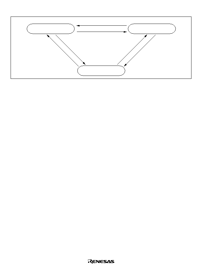
105
Figure 5.5 shows the transitions among the above states.
All interrupts are
unmasked
Only NMI, IRQ , and
IRQ are unmasked
Exception handling,
or I 1, UI 1
a.
b.
2
3
All interrupts are
masked except NMI
c.
UI 0
I 0
Exception handling,
or UI 1
I 0
I 1, UI 0
Figure 5.5 Interrupt Masking State Transitions (Example)
Figure 5.6 is a flowchart showing how interrupts are accepted when UE = 0.
�
If an interrupt condition occurs and the corresponding interrupt enable bit is set to 1, an
interrupt request is sent to the interrupt controller.
�
When the interrupt controller receives one or more interrupt requests, it selects the highest-
priority request, following the IPR interrupt priority settings, and holds other requests pending.
If two or more interrupts with the same IPR setting are requested simultaneously, the interrupt
controller follows the priority order shown in table 5.3.
�
The interrupt controller checks the I bit. If the I bit is cleared to 0, the selected interrupt request
is accepted regardless of its IPR setting, and regardless of the UI bit. If the I bit is set to 1 and
the UI bit is cleared to 0, only NMI and interrupts with priority level 1 are accepted; interrupt
requests with priority level 0 are held pending. If the I bit and UI bit are both set to 1, only
NMI is accepted; all other interrupt requests are held pending.
�
When an interrupt request is accepted, interrupt exception handling starts after execution of the
current instruction has been completed.
�
In interrupt exception handling, PC and CCR are saved to the stack area. The PC value that is
saved indicates the address of the first instruction that will be executed after the return from the
interrupt service routine.
�
The I and UI bits are set to 1 in CCR, masking all interrupts except NMI.
�
The vector address of the accepted interrupt is generated, and the interrupt service routine
starts executing from the address indicated by the contents of the vector address.
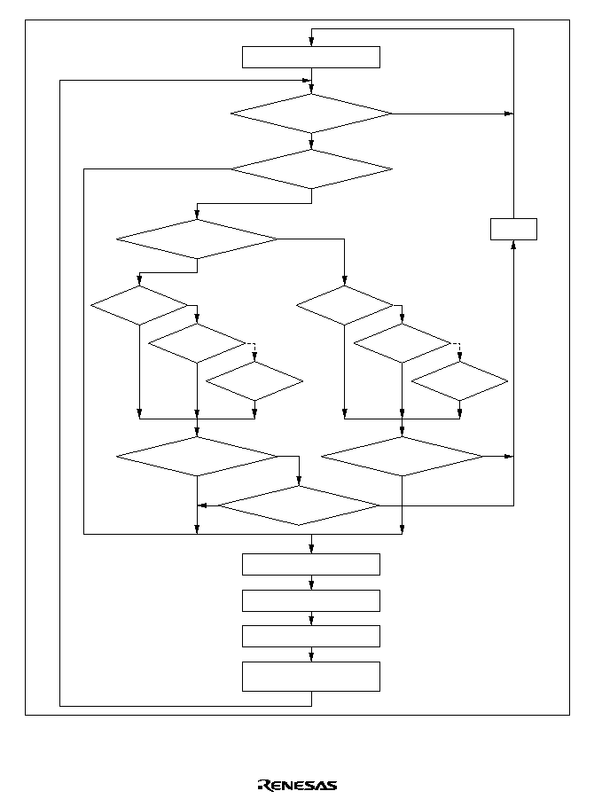
106
Program execution state
Interrupt requested?
NMI
No
Yes
No
Yes
No
Priority level 1?
No
IRQ
0
Yes
No
IRQ
1
Yes
TEI2
Yes
No
IRQ
0
Yes
No
IRQ
1
Yes
TEI2
Yes
No
I = 0
Yes
No
I = 0
Yes
UI = 0
Yes
No
Save PC and CCR
I 1, UI 1
Pending
Branch to interrupt
service routine
Yes
Read vector address
Figure 5.6 Process Up to Interrupt Acceptance when UE = 0
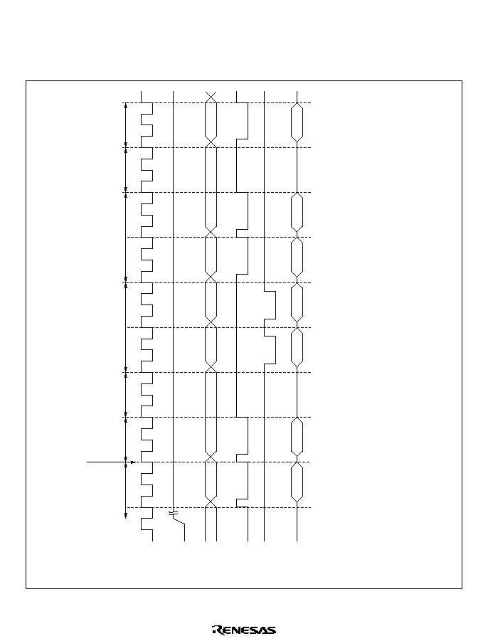
107
5.4.2
Interrupt Sequence
Figure 5.7 shows the interrupt sequence in mode 2 when the program code and stack are in an
external memory area accessed in two states via a 16-bit bus.
Address
bus
Interrupt
request
signal
RD
HWR
D to D
15
0
(1)
(2), (4)
(3)
(5)
(7)
Note: Mode 2, with program code and stack in external memory area accessed in two states via 16-bit bus.
LWR
,
Interrupt level
decision and wait
for end of instruction
Interrupt accepted
Instruction
prefetch
Internal
processing
Stack
V
ector fetch
Internal
processing
Prefetch of
interrupt
service routine
instruction
High
Instruction prefetch address (not executed;
return address, same as PC contents)
Instruction code (not executed)
Instruction prefetch address (not executed)
SP
� 2
SP
� 4
(6), (8)
(9), (1
1)
(10), (12)
(13)
(14)
PC and CCR saved to stack
V
ector address
Starting address of interrupt service routine (contents of
vector address)
Starting address of interrupt service routine; (13) = (10), (12)
First instruction of interrupt service routine
(1)
(2)
(3)
(4)
(5)
(6)
(7)
(8)
(9)
(10)
(1
1)
(12)
(13)
(14)
Figure 5.7 Interrupt Sequence

108
5.4.3
Interrupt Response Time
Table 5.5 indicates the interrupt response time from the occurrence of an interrupt request until the
first instruction of the interrupt service routine is executed.
Table 5.5
Interrupt Response Time
External Memory
On-Chip
8-Bit Bus
16-Bit Bus
No.
Item
Memory
2 States
3 States
2 States
3 States
1
Interrupt priority
decision
2
*
1
2
*
1
2
*
1
2
*
1
2
*
1
2
Maximum number
of states until end of
current instruction
1 to 23
*
5
1 to 27
*
5,
*
6
1 to 41
*
4,
*
6
1 to 23
*
5
1 to 25
*
4,
*
5
3
Saving PC and CCR
to stack
4
8
12
*
4
4
6
*
4
4
Vector fetch
4
8
12
*
4
4
6
*
4
5
Instruction prefetch
*
2
4
8
12
*
4
4
6
*
4
6
Internal processing
*
3
4
4
4
4
4
Total
19 to 41
31 to 57
43 to 83
19 to 41
25 to 49
Notes:
*
1 1 state for internal interrupts.
*
2 Prefetch after the interrupt is accepted and prefetch of the first instruction in the
interrupt service routine.
*
3 Internal processing after the interrupt is accepted and internal processing after vector
fetch.
*
4 The number of states increases if wait states are inserted in external memory access.
*
5 The examples of DIVXS.W Rs,ERd, MULXS.W Rs,ERd.
*
6 The examples of MOV.L Q(d:24,ERs), ERd, MOV.L ERs,Q(d:24,ERd).
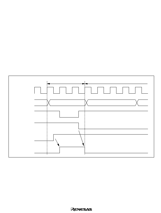
109
5.5
Usage Notes
5.5.1
Contention between Interrupt and Interrupt-Disabling Instruction
When an instruction clears an interrupt enable bit to 0 to disable the interrupt, the interrupt is not
disabled until after execution of the instruction is completed. If an interrupt occurs while a BCLR,
MOV, or other instruction is being executed to clear its interrupt enable bit to 0, at the instant
when execution of the instruction ends the interrupt is still enabled, so its interrupt exception
handling is carried out. If a higher-priority interrupt is also requested, however, interrupt exception
handling for the higher-priority interrupt is carried out, and the lower-priority interrupt is ignored.
This also applies to the clearing of an interrupt flag to 0.
Figure 5.8 shows an example in which an IMIEA bit is cleared to 0 in the 16-bit timer's TISRA
register.
IMIA exception handling
TISRA write cycle by CPU
TISRA address
Internal
address bus
Internal
write signal
IMIEA
IMIA
IMFA interrupt
signal
Figure 5.8 Contention between Interrupt and Interrupt-Disabling Instruction
This type of contention will not occur if the interrupt is masked when the interrupt enable bit or
flag is cleared to 0.

110
5.5.2
Instructions that Inhibit Interrupts
The LDC, ANDC, ORC, and XORC instructions inhibit interrupts. When an interrupt occurs, after
determining the interrupt priority, the interrupt controller requests a CPU interrupt. If the CPU is
currently executing one of these interrupt-inhibiting instructions, however, when the instruction is
completed the CPU always continues by executing the next instruction.
5.5.3
Interrupts during EEPMOV Instruction Execution
The EEPMOV.B and EEPMOV.W instructions differ in their reaction to interrupt requests.
When the EEPMOV.B instruction is executing a transfer, no interrupts are accepted until the
transfer is completed, not even NMI.
When the EEPMOV.W instruction is executing a transfer, interrupt requests other than NMI are
not accepted until the transfer is completed. If NMI is requested, NMI exception handling starts at
a transfer cycle boundary. The PC value saved on the stack is the address of the next instruction.
Programs should be coded as follows to allow for NMI interrupts during EEPMOV.W execution:
L1: EEPMOV.W
MOV.W R4,R4
BNE L1

111
Section 6 Bus Controller
6.1
Overview
The H8/3069F has an on-chip bus controller (BSC) that manages the external address space
divided into eight areas. The bus specifications, such as bus width and number of access states,
can be set independently for each area, enabling multiple memories to be connected easily.
The bus controller also has a bus arbitration function that controls the operation of the internal bus
masters-the CPU, DMA controller (DMAC), and DRAM interface and can release the bus to an
external device.
6.1.1
Features
The features of the bus controller are listed below.
�
Manages external address space in area units
Manages the external space as eight areas (0 to 7) of 128 kbytes in 1-Mbyte modes, or 2
Mbytes in 16-Mbyte modes
Bus specifications can be set independently for each area
DRAM/burst ROM interfaces can be set
�
Basic bus interface
Chip select (
CS
0
to
CS
7
) can be output for areas 0 to 7
8-bit access or 16-bit access can be selected for each area
Two-state access or three-state access can be selected for each area
Program wait states can be inserted for each area
Pin wait insertion capability is provided
�
DRAM interface
DRAM interface can be set for areas 2 to 5
Row address/column address multiplexed output (8/9/10 bits)
2-CAS byte access mode
Burst operation (fast page mode)
T
P
cycle insertion to secure RAS precharging time
Choice of CAS-before-RAS refreshing or self-refreshing
�
Burst ROM interface
Burst ROM interface can be set for area 0
Selection of two- or three-state burst access

112
�
Idle cycle insertion
An idle cycle can be inserted in case of an external read cycle between different areas
An idle cycle can be inserted when an external read cycle is immediately followed by an
external write cycle
�
Bus arbitration function
A built-in bus arbiter grants the bus right to the CPU, DMAC, DRAM interface, or an
external bus master
�
Other features
Refresh counter (refresh timer) can be used as interval timer
Choice of two address update modes
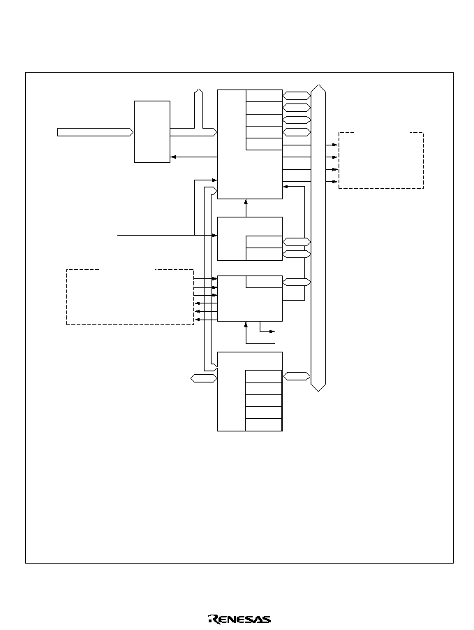
113
6.1.2
Block Diagram
Figure 6.1 shows a block diagram of the bus controller.
Internal address bus
ABWCR
ASTCR
BCR
CSCR
ADRCR
Area
decoder
Chip select
control signals
CS
0
to
CS
7
Bus control
circuit
WCRH
WCRL
BRCR
DRAM control
Legend
DRAM interface
Wait state
controller
WAIT
BACK
BREQ
Internal data bus
CPU bus request signal
DMAC bus request signal
DRAM interface bus request signal
CPU bus acknowledge signal
DMAC bus acknowledge signal
DRAM interface bus acknowledge signal
Bus arbiter
Bus mode control signal
Internal signals
Internal signals
Bus size control signal
Access state control signal
Wait request signal
: Bus width control register
: Access state control register
: DRAM control register A
: DRAM control register B
: Wait control register H
: Wait control register L
: Bus release control register
: Chip select control register
: Refresh timer control/status register
: Refresh timer counter
: Refresh time constant register
ASTCR
DRCRA
DRCRB
WCRH
WCRL
BRCR
CSCR
RTMCSR
RTCNT
RTCOR
ADRCR
: Address control register
ABWCR
DRCRA
DRCRB
RTMCSR
RTCNT
RTCOR
BCR
: Bus control register
Figure 6.1 Block Diagram of Bus Controller

114
6.1.3
Pin Configuration
Table 6.1 summarizes the input/output pins of the bus controller.
Table 6.1
Bus Controller Pins
Name
Abbreviation
I/O
Function
Chip select 0 to 7
CS
0
to
CS
7
Output
Strobe signals selecting areas 0 to 7
Address strobe
AS
Output
Strobe signal indicating valid address output
on the address bus
Read
RD
Output
Strobe signal indicating reading from the
external address space
High write
HWR
Output
Strobe signal indicating writing to the external
address space, with valid data on the upper
data bus (D
15
to D
8
)
Low write
LWR
Output
Strobe signal indicating writing to the external
address space, with valid data on the lower
data bus (D
7
to D
0
)
Wait
WAIT
Input
Wait request signal for access to external
three-state access areas
Bus request
BREQ
Input
Request signal for releasing the bus to an
external device
Bus acknowledge
BACK
Output
Acknowledge signal indicating release of the
bus to an external device

115
6.1.4
Register Configuration
Table 6.2 summarizes the bus controller's registers.
Table 6.2
Bus Controller Registers
Address
*
1
Name
Abbreviation
R/W
Initial Value
H'EE020
Bus width control register
ABWCR
R/W
H'FF
*
2
H'EE021
Access state control register
ASTCR
R/W
H'FF
H'EE022
Wait control register H
WCRH
R/W
H'FF
H'EE023
Wait control register L
WCRL
R/W
H'FF
H'EE013
Bus release control register
BRCR
R/W
H'FE
*
3
H'EE01F
Chip select control register
CSCR
R/W
H'0F
H'EE01E
Address control register
ADRCR
R/W
H'FF
H'EE024
Bus control register
BCR
R/W
H'C6
H'EE026
DRAM control register A
DRCRA
R/W
H'10
H'EE027
DRAM control register B
DRCRB
R/W
H'08
H'EE028
Refresh timer control/status register
RTMCSR
R(W)
*
4
H'07
H'EE029
Refresh timer counter
RTCNT
R/W
H'00
H'EE02A
Refresh time constant register
RTCOR
R/W
H'FF
Notes:
*
1 Lower 20 bits of the address in advanced mode.
*
2 In modes 2 and 4, the initial value is H'00.
*
3 In modes 3 and 4, the initial value is H'EE.
*
4 For Bit 7, only 0 can be written to clear the flag.

116
6.2
Register Descriptions
6.2.1
Bus Width Control Register (ABWCR)
ABWCR is an 8-bit readable/writable register that selects 8-bit or 16-bit access for each area.
7
ABW7
1
R/W
0
R/W
6
ABW6
1
R/W
0
R/W
5
ABW5
1
R/W
0
R/W
4
ABW4
1
R/W
0
R/W
3
ABW3
1
R/W
0
R/W
2
ABW2
1
R/W
0
R/W
1
ABW1
1
R/W
0
R/W
0
ABW0
1
R/W
0
R/W
Bit
Modes
1, 3, 5,
and 7
Initial value
Read/Write
Initial value
Read/Write
Modes
2 and 4
When ABWCR contains H'FF (selecting 8-bit access for all areas), the chip operates in 8-bit bus
mode: the upper data bus (D
15
to D
8
) is valid, and port 4 is an input/output port. When at least one
bit is cleared to 0 in ABWCR, the chip operates in 16-bit bus mode with a 16-bit data bus (D
15
to
D
0
). In modes 1, 3, 5, and 7, ABWCR is initialized to H'FF by a reset and in hardware standby
mode. In modes 2 and 4, ABWCR is initialized to H'00 by a reset and in hardware standby mode.
It is not initialized in software standby mode.
Bits 7 to 0--Area 7 to 0 Bus Width Control (ABW7 to ABW0): These bits select 8-bit access or
16-bit access for the corresponding areas.
Bits 7 to 0
ABW7 to ABW0
Description
0
Areas 7 to 0 are 16-bit access areas
1
Areas 7 to 0 are 8-bit access areas
ABWCR specifies the data bus width of external memory areas. The data bus width of on-chip
memory and registers is fixed, and does not depend on ABWCR settings. These settings are
therefore meaningless in the single-chip modes (mode 7).
117
6.2.2
Access State Control Register (ASTCR)
ASTCR is an 8-bit readable/writable register that selects whether each area is accessed in two
states or three states.
AST3
AST2
AST1
AST0
1
Initial value
1
1
1
1
1
1
1
Read/Write
R/W
R/W
R/W
R/W
R/W
R/W
R/W
R/W
7
6
5
4
3
2
1
0
Bits selecting number of states for access to each area
AST7
AST6
AST5
AST4
Bit
ASTCR is initialized to H'FF by a reset and in hardware standby mode. It is not initialized in
software standby mode.
Bits 7 to 0--Area 7 to 0 Access State Control (AST7 to AST0): These bits select whether the
corresponding area is accessed in two or three states.
Bits 7 to 0
AST7 to AST0
Description
0
Areas 7 to 0 are accessed in two states
1
Areas 7 to 0 are accessed in three states
(Initial value)
ASTCR specifies the number of states in which external areas are accessed. On-chip memory and
registers are accessed in a fixed number of states that does not depend on ASTCR settings. These
settings are therefore meaningless in the single-chip modes (mode 7).
When the corresponding area is designated as DRAM space by bits DRAS2 to DRAS0 in DRAM
control register A (DRCRA), the number of access states does not depend on the AST bit setting.
When an AST bit is cleared to 0, programmable wait insertion is not performed.
6.2.3
Wait Control Registers H and L (WCRH, WCRL)
WCRH and WCRL are 8-bit readable/writable registers that select the number of program wait
states for each area.
On-chip memory and registers are accessed in a fixed number of states that does not depend on
WCRH/WCRL settings.
WCRH and WCRL are initialized to H'FF by a reset and in hardware standby mode. They are not
initialized in software standby mode.

118
WCRH
W51
W50
W41
W40
1
Initial value
1
1
1
1
1
1
1
Read/Write
R/W
R/W
R/W
R/W
R/W
R/W
R/W
R/W
7
6
5
4
3
2
1
0
W71
W70
W61
W60
Bit
Bits 7 and 6--Area 7 Wait Control 1 and 0 (W71, W70): These bits select the number of
program wait states when area 7 in external space is accessed while the AST7 bit in ASTCR is set
to 1.
Bit 7
W71
Bit 6
W70
Description
0
0
Program wait not inserted when external space area 7 is accessed
1
1 program wait state inserted when external space area 7 is accessed
1
0
2 program wait states inserted when external space area 7 is accessed
1
3 program wait states inserted when external space area 7 is accessed
(Initial value)
Bits 5 and 4--Area 6 Wait Control 1 and 0 (W61, W60): These bits select the number of
program wait states when area 6 in external space is accessed while the AST6 bit in ASTCR is set
to 1.
Bit 5
W61
Bit 4
W60
Description
0
0
Program wait not inserted when external space area 6 is accessed
1
1 program wait state inserted when external space area 6 is accessed
1
0
2 program wait states inserted when external space area 6 is accessed
1
3 program wait states inserted when external space area 6 is accessed
(Initial value)
Bits 3 and 2--Area 5 Wait Control 1 and 0 (W51, W50): These bits select the number of
program wait states when area 5 in external space is accessed while the AST5 bit in ASTCR is set
to 1.

119
Bit 3
W51
Bit 2
W50
Description
0
0
Program wait not inserted when external space area 5 is accessed
1
1 program wait state inserted when external space area 5 is accessed
1
0
2 program wait states inserted when external space area 5 is accessed
1
3 program wait states inserted when external space area 5 is accessed
(Initial value)
Bits 1 and 0--Area 4 Wait Control 1 and 0 (W41, W40): These bits select the number of
program wait states when area 4 in external space is accessed while the AST4 bit in ASTCR is set
to 1.
Bit 1
W41
Bit 0
W40
Description
0
0
Program wait not inserted when external space area 4 is accessed
1
1 program wait state inserted when external space area 4 is accessed
1
0
2 program wait states inserted when external space area 4 is accessed
1
3 program wait states inserted when external space area 4 is accessed
(Initial value)
WCRL
W11
W10
W01
W00
1
Initial value
1
1
1
1
1
1
1
Read/Write
R/W
R/W
R/W
R/W
R/W
R/W
R/W
R/W
7
6
5
4
3
2
1
0
W31
W30
W21
W20
Bit
Bits 7 and 6--Area 3 Wait Control 1 and 0 (W31, W30): These bits select the number of
program wait states when area 3 in external space is accessed while the AST3 bit in ASTCR is set
to 1.
Bit 7
W31
Bit 6
W30
Description
0
0
Program wait not inserted when external space area 3 is accessed
1
1 program wait state inserted when external space area 3 is accessed
1
0
2 program wait states inserted when external space area 3 is accessed
1
3 program wait states inserted when external space area 3 is accessed
(Initial value)

120
Bits 5 and 4--Area 2 Wait Control 1 and 0 (W21, W20): These bits select the number of
program wait states when area 2 in external space is accessed while the AST2 bit in ASTCR is set
to 1.
Bit 5
W21
Bit 4
W20
Description
0
0
Program wait not inserted when external space area 2 is accessed
1
1 program wait state inserted when external space area 2 is accessed
1
0
2 program wait states inserted when external space area 2 is accessed
1
3 program wait states inserted when external space area 2 is accessed
(Initial value)
Bits 3 and 2--Area 1 Wait Control 1 and 0 (W11, W10): These bits select the number of
program wait states when area 1 in external space is accessed while the AST1 bit in ASTCR is set
to 1.
Bit 3
W11
Bit 2
W10
Description
0
0
Program wait not inserted when external space area 1 is accessed
1
1 program wait state inserted when external space area 1 is accessed
1
0
2 program wait states inserted when external space area 1 is accessed
1
3 program wait states inserted when external space area 1 is accessed
(Initial value)
Bits 1 and 0--Area 0 Wait Control 1 and 0 (W01, W00): These bits select the number of
program wait states when area 0 in external space is accessed while the AST0 bit in ASTCR is set
to 1.
Bit 1
W01
Bit 0
W00
Description
0
0
Program wait not inserted when external space area 0 is accessed
1
1 program wait state inserted when external space area 0 is accessed
1
0
2 program wait states inserted when external space area 0 is accessed
1
3 program wait states inserted when external space area 0 is accessed
(Initial value)
121
6.2.4
Bus Release Control Register (BRCR)
BRCR is an 8-bit readable/writable register that enables address output on bus lines A
23
to A
20
and
enables or disables release of the bus to an external device.
7
A23E
1
--
1
R/W
1
R/W
Address 23 to 20 enable
These bits enable PA
7
to PA
4
to be
used for A
23
to A
20
address output
6
A22E
1
--
1
R/W
1
R/W
5
A21E
1
--
1
R/W
1
R/W
4
A20E
1
--
0
--
1
R/W
3
--
1
--
1
--
1
--
2
--
1
--
1
--
1
--
1
--
1
--
1
--
1
--
0
BRLE
0
R/W
0
R/W
0
R/W
Bit
Modes
1, 2,
and 7
Initial value
Read/Write
Initial value
Read/Write
Initial value
Read/Write
Modes
3 and 4
Mode 5
Reserved bits
Bus release enable
Enables or disables
release of the bus
to an external device
BRCR is initialized to H'FE in modes 1, 2, 5, and 7, and to H'EE in modes 3 and 4, by a reset and
in hardware standby mode. It is not initialized in software standby mode.
Bit 7--Address 23 Enable (A23E): Enables PA
4
to be used as the A
23
address output pin.
Writing 0 in this bit enables A
23
output from PA
4
. In modes other than 3, 4, and 5, this bit cannot
be modified and PA
4
has its ordinary port functions.
Bit 7
A23E
Description
0
PA
4
is the A
23
address output pin
1
PA
4
is an input/output pin
(Initial value)
Bit 6--Address 22 Enable (A22E): Enables PA
5
to be used as the A
22
address output pin.
Writing 0 in this bit enables A
22
output from PA
5
. In modes other than 3, 4, and 5, this bit cannot
be modified and PA
5
has its ordinary port functions.
Bit 6
A22E
Description
0
PA
5
is the A
22
address output pin
1
PA
5
is an input/output pin
(Initial value)

122
Bit 5--Address 21 Enable (A21E): Enables PA
6
to be used as the A
21
address output pin.
Writing 0 in this bit enables A
21
output from PA
6
. In modes other than 3, 4, and 5, this bit cannot
be modified and PA
6
has its ordinary port functions.
Bit 5
A21E
Description
0
PA
6
is the A
21
address output pin
1
PA
6
is an input/output pin
(Initial value)
Bit 4--Address 20 Enable (A20E): Enables PA
7
to be used as the A
20
address output pin.
Writing 0 in this bit enables A
20
output from PA
7
. This bit can only be modified in mode 5.
Bit 4
A20E
Description
0
PA
7
is the A
20
address output pin (Initial value when in mode 3 or 4)
1
PA
7
is an input/output pin (Initial value when in mode 1, 2, 5, or 7)
Bits 3 to 1--Reserved: These bits cannot be modified and are always read as 1.
Bit 0--Bus Release Enable (BRLE): Enables or disables release of the bus to an external device.
Bit 0
BRLE
Description
0
The bus cannot be released to an external device
BREQ
and
BACK
can be used as input/output pins
(Initial value)
1
The bus can be released to an external device
6.2.5
Bus Control Register (BCR)
BRSTS0
EMC
RDEA
WAITE
1
Initial value
1
0
0
0
1
1
0
Read/Write
R/W
R/W
R/W
R/W
R/W
R/W
R/W
R/W
7
6
5
4
3
2
1
0
ICIS1
ICIS0
BROME BRSTS1
Bit
BCR is an 8-bit readable/writable register that enables or disables idle cycle insertion, selects the
address map, selects the area division unit, and enables or disables
WAIT pin input.
BCR is initialized to H'C6 by a reset and in hardware standby mode. It is not initialized in
software standby mode.

123
Bit 7--Idle Cycle Insertion 1 (ICIS1): Selects whether one idle cycle state is to be inserted
between bus cycles in case of consecutive external read cycles for different areas.
Bit 7
ICIS1
Description
0
No idle cycle inserted in case of consecutive external read cycles for different
areas
1
Idle cycle inserted in case of consecutive external read cycles for different
areas
(Initial value)
Bit 6--Idle Cycle Insertion 0 (ICIS0): Selects whether one idle cycle state is to be inserted
between bus cycles in case of consecutive external read and write cycles.
Bit 6
ICIS0
Description
0
No idle cycle inserted in case of consecutive external read and write cycles
1
Idle cycle inserted in case of consecutive external read and write cycles
(Initial value)
Bit 5--Burst ROM Enable (BROME): Selects whether area 0 is a burst ROM interface area.
Bit 5
BROME
Description
0
Area 0 is a basic bus interface area
(Initial value)
1
Area 0 is a burst ROM interface area
Bit 4--Burst Cycle Select 1 (BRSTS1): Selects the number of burst cycle states for the burst
ROM interface.
Bit 4
BRSTS1
Description
0
Burst access cycle comprises 2 states
(Initial value)
1
Burst access cycle comprises 3 states

124
Bit 3--Burst Cycle Select 0 (BRSTS0): Selects the number of words that can be accessed in a
burst ROM interface burst access.
Bit 3
BRSTS0
Description
0
Max. 4 words in burst access (burst access on match of address bits above A3)
(Initial value)
1
Max. 8 words in burst access (burst access on match of address bits above A4)
Bit 2--Expansion Memory Map Control (EMC): Selects either of the two memory maps.
Bit 2
EMC
Description
0
Selects the memory map shown in figure 3.2: see section 3.6, Memory Map
*
in
Each Operating Mode
1
Selects the memory map shown in figure 3.1: see section 3.6, Memory Map
*
in
Each Operating Mode
(Initial value)
Note: * When the memory map is switched using EMC, the following area combinations in the
on-chip RAM area cannot be used.
(EMC bit = 1)
(EMC bit = 0)
Mode 1 or 2
(1)
H'FDEE0 to H'FDF1F
H'FBEE0 to H'FBF1F
(2)
H'FFE80 to H'FFEDF
H'FFF80 to H'FFFDF
(3)
H'FFEE0 to H'FFF1F
H'FDEE0 to H'FDF1F
Mode 3 or 4
(1)
H'FFDEE0 to H'FFDF1F
H'FFBEE0 to H'FFBF1F
(2)
H'FFFE80 to H'FFFEDF
H'FFFF80 to H'FFFFDF
(3)
H'FFFEE0 to H'FFFF1F
H'FFDEE0 to H'FFDF1F
Mode 5
(1)
H'FFDEE0 to H'FFDF1F
H'FFBEE0 to H'FFBF1F
(2)
H'FFFE80 to H'FFFEDF
H'FFFF80 to H'FFFFDF
(3)
H'FFFEE0 to H'FFFF1F
H'FFDEE0 to H'FFDF1F
Mode 7
(1)
H'FDEE0 to H'FDF1F
H'FBEE0 to H'FBF1F
(2)
H'FFE80 to H'FFEDF
H'FFF80 to H'FFFDF
(3)
H'FFEE0 to H'FFF1F
H'FDEE0 to H'FDF1F
When EMC is cleared to 0, addresses of some internal I/O registers are moved. For details, refer
to appendix B.2, Addresses (EMC = 0).

125
When the RDEA bit is 0, EMC must not be cleared to 0.
Bit 1--Area Division Unit Select (RDEA): Selects the memory map area division units. This bit
is valid in modes 3, 4, and 5, and is invalid in modes 1, 2, and 7.
When the EMC bit is 0, RDEA must not be cleared to 0.
Bit 1
RDEA
Description
0
Area divisions are as follows:
Area 0: 2 Mbytes
Area 4: 1.93 Mbytes
Area 1: 2 Mbytes
Area 5: 4 kbytes
Area 2: 8 Mbytes
Area 6: 23.75 kbytes
Area 3: 2 Mbytes
Area 7: 22 bytes
1
Areas 0 to 7 are the same size (2 Mbytes)
(Initial value)
Bit 0--WAIT Pin Enable (WAITE): Enables or disables wait insertion by means of the
WAIT
pin.
Bit 0
WAITE
Description
0
WAIT
pin wait input is disabled, and the
WAIT
pin can be used as an
input/output port
(Initial value)
1
WAIT
pin wait input is enabled
126
6.2.6
Chip Select Control Register (CSCR)
CSCR is an 8-bit readable/writable register that enables or disables output of chip select signals
(
CS
7
to
CS
4
).
If output of a chip select signal is enabled by a setting in this register, the corresponding pin
functions as a chip select signal (
CS
7
to
CS
4
) output regardless of any other settings. CSCR cannot
be modified in single-chip mode.
--
--
--
--
0
Initial value
0
0
0
1
1
1
1
Read/Write
--
--
--
--
R/W
R/W
R/W
R/W
7
6
5
4
3
2
1
0
Reserved bits
CS7E
CS6E
CS5E
CS4E
Chip select 7 to 4 enable
These bits enable or disable
chip select signal output
Bit
CSCR is initialized to H'0F by a reset and in hardware standby mode. It is not initialized in
software standby mode.
Bits 7 to 4--Chip Select 7 to 4 Enable (CS7E to CS4E): These bits enable or disable output of
the corresponding chip select signal.
Bit n
CSnE
Description
0
Output of chip select signal
CSn
is disabled
(Initial value)
1
Output of chip select signal
CSn
is enabled
Note:
n = 7 to 4
Bits 3 to 0--Reserved: These bits cannot be modified and are always read as 1.

127
6.2.7
DRAM Control Register A (DRCRA)
BE
RDM
SRFMD
RFSHE
0
Initial value
0
0
1
0
0
0
0
Read/Write
R/W
R/W
R/W
R/W
R/W
R/W
R/W
--
7
6
5
4
3
2
1
0
DRAS2
DRAS1
DRAS0
--
Bit
DRCRA is an 8-bit readable/writable register that selects the areas that have a DRAM interface
function, and the access mode, and enables or disables self-refreshing and refresh pin output.
DRCRA is initialized to H'10 by a reset and in hardware standby mode. It is not initialized in
software standby mode.
Bits 7 to 5--DRAM Area Select (DRAS2 to DRAS0): These bits select which of areas 2 to 5 are
to function as DRAM interface areas (DRAM space) in expanded mode, and at the same time
select the
RAS output pin corresponding to each DRAM space.
Description
Bit 7
DRAS2
Bit 6
DRAS1
Bit 5
DRAS0 Area 5
Area 4
Area 3
Area 2
0
0
0
Normal
Normal
Normal
Normal
1
Normal
Normal
Normal
DRAM space
(
CS
2
)
1
0
Normal
Normal
DRAM space
(
CS
3
)
DRAM space
(
CS
2
)
1
Normal
Normal
DRAM space
(
CS
2
)
*
DRAM space
(
CS
2
)
*
1
0
0
Normal
DRAM space
(
CS
4
)
DRAM space
(
CS
3
)
DRAM space
(
CS
2
)
1
DRAM space
(
CS
5
)
DRAM space
(
CS
4
)
DRAM space
(
CS
3
)
DRAM space
(
CS
2
)
1
0
DRAM space
(
CS
4
)
*
DRAM space
(
CS
4
)
*
DRAM space
(
CS
2
)
*
DRAM space
(
CS
2
)
*
1
DRAM space
(
CS
2
)
*
DRAM space
(
CS
2
)
*
DRAM space
(
CS
2
)
*
DRAM space
(
CS
2
)
*
Note:
*
A single
CSn
pin serves as a common
RAS
output pin for a number of areas. Unused
CSn
pins can be used as input/output ports.
When any of bits DRAS2 to DRAS0 is set to 1 in expanded mode, it is not possible to write to
DRCRB, RTMCSR, RTCNT, or RTCOR. However, 0 can be written to the CMF flag in
RTMCSR to clear the flag.

128
When an arbitrary value has been set in DRAS2 to DRAS0, a write of a different value other than
000 must not be performed.
Bit 4--Reserved: This bit cannot be modified and is always read as 1.
Bit 3--Burst Access Enable (BE): Enables or disables burst access to DRAM space. DRAM
space burst access is performed in fast page mode.
Bit 3
BE
Description
0
Burst disabled (always full access)
(Initial value)
1
DRAM space access performed in fast page mode
Bit 2--RAS Down Mode (RDM): Selects whether to wait for the next DRAM access with the
RAS signal held low (RAS down mode), or to drive the RAS signal high again (RAS up mode),
when burst access is enabled for DRAM space (BE = 1), and access to DRAM is interrupted.
Caution is required when the
HWR and LWR are used as the UCAS and LCAS output pins. For
details, see RAS Down Mode and RAS Up Mode in section 6.5.10, Burst Operation.
Bit 2
RDM
Description
0
DRAM interface: RAS up mode selected
(Initial value)
1
DRAM interface: RAS down mode selected
Bit 1--Self-Refresh Mode (SRFMD): Specifies DRAM self-refreshing in software standby
mode.
When any of areas 2 to 5 is designated as DRAM space, DRAM self-refreshing is possible when a
transition is made to software standby mode after the SRFMD bit has been set to 1.
The normal access state is restored when software standby mode is exited, regardless of the
SRFMD setting.
Bit 1
SRFMD
Description
0
DRAM self-refreshing disabled in software standby mode
(Initial value)
1
DRAM self-refreshing enabled in software standby mode

129
Bit 0--Refresh Pin Enable (RFSHE): Enables or disables
RFSH pin refresh signal output. If
areas 2 to 5 are not designated as DRAM space, this bit should not be set to 1.
Bit 0
RFSHE
Description
0
RFSH
pin refresh signal output disabled
(Initial value)
(
RFSH
pin can be used as input/output port)
1
RFSH
pin refresh signal output enabled
6.2.8
DRAM Control Register B (DRCRB)
--
TPC
RCW
RLW
0
Initial value
0
0
0
1
0
0
0
Read/Write
--
R/W
R/W
R/W
R/W
R/W
R/W
R/W
7
6
5
4
3
2
1
0
MXC1
MXC0
CSEL
RCYCE
Bit
DRCRB is an 8-bit readable/writable register that selects the number of address multiplex column
address bits for the DRAM interface, the column address strobe output pin, enabling or disabling
of refresh cycle insertion, the number of precharge cycles, enabling or disabling of wait state
insertion between
RAS and CAS, and enabling or disabling of wait state insertion in refresh
cycles.
DRCRB is initialized to H'08 by a reset and in hardware standby mode. It is not initialized in
software standby mode.
The settings in this register are invalid when bits DRAS2 to DRAS0 in DRCRA are all 0.
Bits 7 and 6--Multiplex Control 1 and 0 (MXC1, MXC0): These bits select the row
address/column address multiplexing method used on the DRAM interface. In burst operation, the
row address used for comparison is determined by the setting of these bits and the bus width of the
relevant area set in ABWCR.

130
Bit 7
MXC1
Bit 6
MXC0
Description
0
0
Column address: 8 bits
Compared address:
Modes 1, 2
8-bit access space
A
19
to A
8
16-bit access space
A
19
to A
9
Modes 3, 4, 5
8-bit access space
A
23
to A
8
16-bit access space
A
23
to A
9
1
Column address: 9 bits
Compared address:
Modes 1, 2
8-bit access space
A
19
to A
9
16-bit access space
A
19
to A
10
Modes 3, 4, 5
8-bit access space
A
23
to A
9
16-bit access space
A
23
to A
10
1
0
Column address: 10 bits
Compared address:
Modes 1, 2
8-bit access space
A
19
to A
10
16-bit access space
A
19
to A
11
Modes 3, 4, 5
8-bit access space
A
23
to A
10
16-bit access space
A
23
to A
11
1
Illegal setting
Bit 5--
CAS Output Pin Select (CSEL): Selects the UCAS and LCAS output pins when areas 2
to 5 are designated as DRAM space.
Bit 5
CSEL
Description
0
PB4 and PB5 selected as
UCAS
and
LCAS
output pins
(Initial value)
1
HWR
and
LWR
selected as
UCAS
and
LCAS
output pins
Bit 4--Refresh Cycle Enable (RCYCE): Enables or disables CAS-before-RAS refresh cycle
insertion. When none of areas 2 to 5 has been designated as DRAM space, refresh cycles are not
inserted regardless of the setting of this bit.
Bit 4
RCYCE
Description
0
Refresh cycles disabled
(Initial value)
1
DRAM refresh cycles enabled

131
Bit 3--Reserved: This bit cannot be modified and is always read as 1.
Bit 2--TP Cycle Control (TPC): Selects whether a 1-state or two-state precharge cycle (T
P
) is to
be used for DRAM read/write cycles and CAS-before-RAS refresh cycles.
The setting of this bit does not affect the self-refresh function.
Bit 2
TPC
Description
0
1-state precharge cycle inserted
(Initial value)
1
2-state precharge cycle inserted
Bit 1--
RAS-CAS Wait (RCW): Controls wait state (Trw) insertion between T
r
and T
c1
in DRAM
read/write cycles. The setting of this bit does not affect refresh cycles.
Bit 1
RCW
Description
0
Wait state (Trw) insertion disabled
(Initial value)
1
One wait state (Trw) inserted
Bit 0--Refresh Cycle Wait Control (RLW): Controls wait state (T
RW
) insertion for CAS-before-
RAS refresh cycles. The setting of this bit does not affect DRAM read/write cycles.
Bit 0
RLW
Description
0
Wait state (T
RW
) insertion disabled
(Initial value)
1
One wait state (T
RW
) inserted
6.2.9
Refresh Timer Control/Status Register (RTMCSR)
CKS0
--
--
--
0
Initial value
0
0
0
0
1
1
1
Read/Write
R/W
--
--
--
R(W)
*
R/W
R/W
R/W
7
6
5
4
3
2
1
0
CMF
CMIE
CKS2
CKS1
Bit
RTMCSR is an 8-bit readable/writable register that selects the refresh timer counter clock. When
the refresh timer is used as an interval timer, RTMCSR also enables or disables interrupt requests.
Bits 7 and 6 of RTMCSR are initialized to 0 by a reset and in the standby modes. Bits 5 to 3 are
initialized to 0 by a reset and in hardware standby mode; they are not initialized in software
standby mode.

132
Note: * Only 0 can be written to clear the flag.
Bit 7--Compare Match Flag (CMF): Status flag that indicates a match between the values of
RTCNT and RTCOR.
Bit 7
CMF
Description
0
[Clearing conditions]
When the chip is reset and in standby mode
Read CMF when CMF = 1, then write 0 in CMF
(Initial value)
1
[Setting condition]
When RTCNT = RTCOR
Bit 6--Compare Match Interrupt Enable (CMIE): Enables or disables the CMI interrupt
requested when the CMF flag is set to 1 in RTMCSR. The CMIE bit is always cleared to 0 when
any of areas 2 to 5 is designated as DRAM space.
Bit 6
CMIE
Description
0
The CMI interrupt requested by CMF is disabled
(Initial value)
1
The CMI interrupt requested by CMF is enabled
Bits 5 to 3--Refresh Counter Clock Select (CKS2 to CKS0): These bits select the clock to be
input to RTCNT from among 7 clocks obtained by dividing the system clock (
). When the input
clock is selected with bits CKS2 to CKS0, RTCNT begins counting up.
Bit 5
CKS2
Bit 4
CKS1
Bit 3
CKS0 Description
0
0
0
Count operation halted
(Initial value)
1
/2 used as counter clock
1
0
/8 used as counter clock
1
/32 used as counter clock
1
0
0
/128 used as counter clock
1
/512 used as counter clock
1
0
/2048 used as counter clock
1
/4096 used as counter clock
Bits 2 to 0--Reserved: These bits cannot be modified and are always read as 1.

133
6.2.10
Refresh Timer Counter (RTCNT)
0
Initial value
0
0
0
0
0
0
0
Read/Write
R/W
R/W
R/W
R/W
R/W
R/W
R/W
R/W
7
6
5
4
3
2
1
0
Bit
RTCNT is an 8-bit readable/writable up-counter.
RTCNT is incremented by an internal clock selected by bits CKS2 to CKS0 in RTMCSR. When
RTCNT matches RTCOR (compare match), the CMF flag in RTMCSR is set to 1 and RTCNT is
cleared to H'00. If the RCYCE bit in DRCRB is set to 1 at this time, a refresh cycle is started.
Also, if the CMIE bit in RTMCSR is set to 1, a compare match interrupt (CMI) is generated.
RTCNT is initialized to H'00 by a reset and in standby mode.
6.2.11
Refresh Time Constant Register (RTCOR)
1
Initial value
1
1
1
1
1
1
1
Read/Write
R/W
R/W
R/W
R/W
R/W
R/W
R/W
R/W
7
6
5
4
3
2
1
0
Bit
RTCOR is an 8-bit readable/writable register that determines the interval at which RTCNT is
cleared.
RTCOR and RTCNT are constantly compared. When their values match, the CMF flag is set to 1
in RTMCSR, and RTCNT is simultaneously cleared to H'00.
RTCOR is initialized to H'FF by a reset and in hardware standby mode. It is not initialized in
software standby mode.
Note:
Only byte access can be used on this register.

134
6.2.12
Address Control Register (ADRCR)
ADRCR is an 8-bit readable/writable register that selects either address update mode 1 or address
update mode 2 as the address output method.
7
--
1
--
6
--
1
--
5
--
1
--
4
--
1
--
3
--
1
--
2
--
1
--
1
--
1
--
0
ADRCTL
1
R/W
Bit
Initial value
R/W
Reserved bits
Address control
Selects address update
mode 1 or address
update mode 2
ADRCR is initialized to H'FF by a reset and in hardware standby mode. It is not initialized in
software standby mode.
Bits 7 to 1--Reserved: Read-only bits, always read as 1.
Bit 0--Address Control (ADRCTL): Selects the address output method.
Bit 0
ADRCTL
Description
0
Address update mode 2 is selected
1
Address update mode 1 is selected
(Initial value)
135
6.3
Operation
6.3.1
Area Division
The external address space is divided into areas 0 to 7. Each area has a size of 128 kbytes in the 1-
Mbyte modes, or 2-Mbytes in the 16-Mbyte modes. Figure 6.2 shows a general view of the
memory map.
H' 00000
H' 1FFFF
H' 20000
H' 3FFFF
H' 40000
H' 5FFFF
H' 60000
H' 7FFFF
H' 80000
H' 9FFFF
H' A0000
H' BFFFF
H' C0000
H' DFFFF
H' E0000
H' FFFFF
Area 0 (128 kbytes)
Area 1 (128 kbytes)
Area 2 (128 kbytes)
Area 3 (128 kbytes)
Area 4 (128 kbytes)
Area 5 (128 kbytes)
Area 6 (128 kbytes)
Area 7 (128 kbytes)
H' 000000
H' 1FFFFF
H' 200000
H' 3FFFFF
H' 400000
H' 5FFFFF
H' 600000
H' 7FFFFF
H' 800000
H' 9FFFFF
H' A00000
H' BFFFFF
H' C00000
H' DFFFFF
H' E00000
H' FFFFFF
Area 0 (2 Mbytes)
Area 1 (2 Mbytes)
Area 2 (2 Mbytes)
Area 3 (2 Mbytes)
Area 4 (2 Mbytes)
Area 5 (2 Mbytes)
Area 6 (2 Mbytes)
Area 7 (2 Mbytes)
(a) 1-Mbyte modes (modes 1 and 2)
(b) 16-Mbyte modes (modes 3, 4, and 5)
Figure 6.2 Access Area Map for Each Operating Mode
Chip select signals (
CS
0
to
CS
7
) can be output for areas 0 to 7. The bus specifications for each
area are selected in ABWCR, ASTCR, WCRH, and WCRL.
In 16-Mbyte mode, the area division units can be selected with the RDEA bit in BCR.
136
H'000000
H'1FFFFF
H'200000
H'3FFFFF
H'400000
H'5FFFFF
H'600000
H'7FFFFF
H'800000
H'9FFFFF
H'A00000
H'BFFFFF
H'C00000
H'DFFFFF
H'E00000
H'FEE000
H'FEE0FF
H'FEE100
H'FF7FFF
H'FF8000
H'FF8FFF
H'FF9000
H'FFEF1F
H'FFEF20
H'FFFEFF
H'FFFF00
H'FFFF1F
H'FFFF20
H'FFFFE9
H'FFFFEA
H'FFFFFF
Area 0
2 Mbytes
Area 1
2 Mbytes
Area 2
2 Mbytes
Area 3
2 Mbytes
Area 4
2 Mbytes
Area 5
2 Mbytes
Area 6
2 Mbytes
Area 7
1.93 Mbytes
On-chip registers (1)
Area 7
67.5 kbytes
On-chip RAM
4 kbytes
On-chip registers (2)
Area 7
22 bytes
Area 0
2 Mbytes
Area 1
2 Mbytes
Area 2
8 Mbytes
Area 3
2 Mbytes
Area 4
1.93 Mbytes
Area 5
4 kbytes
On-chip RAM
4 kbytes
*
On-chip registers (2)
Area 7
22 bytes
Area 6
23.75 kbytes
On-chip registers (1)
2 Mbytes
2 Mbytes
2 Mbytes
2 Mbytes
2 Mbytes
2 Mbytes
2 Mbytes
2 Mbytes
Absolute
address 16 bits
Absolute
address 8 bits
(A) Memory map when RDEA = 1
(b) Memory map when RDEA = 0
Reserved 39.75 kbytes
Note:
*
Area 6 when the RAME bit is cleared.
Figure 6.3 Memory Map in 16-Mbyte Mode

137
6.3.2
Bus Specifications
The external space bus specifications consist of three elements: (1) bus width, (2) number of
access states, and (3) number of program wait states.
The bus width and number of access states for on-chip memory and registers are fixed, and are not
affected by the bus controller.
Bus Width: A bus width of 8 or 16 bits can be selected with ABWCR. An area for which an 8-bit
bus is selected functions as an 8-bit access space, and an area for which a 16-bit bus is selected
functions as a16-bit access space.
If all areas are designated for 8-bit access, 8-bit bus mode is set; if any area is designated for 16-
bit access, 16-bit bus mode is set.
Number of Access States: Two or three access states can be selected with ASTCR. An area for
which two-state access is selected functions as a two-state access space, and an area for which
three-state access is selected functions as a three-state access space.
DRAM space is accessed in four states regardless of the ASTCR settings.
When two-state access space is designated, wait insertion is disabled.
Number of Program Wait States: When three-state access space is designated in ASTCR, the
number of program wait states to be inserted automatically is selected with WCRH and WCRL.
From 0 to 3 program wait states can be selected.
When ASTCR is cleared to 0 for DRAM space, a program wait (T
c1
-T
c2
wait) is not inserted.
Also, no program wait is inserted in burst ROM space burst cycles.
Table 6.3 shows the bus specifications for each basic bus interface area.

138
Table 6.3
Bus Specifications for Each Area (Basic Bus Interface)
ABWCR ASTCR WCRH/WCRL
Bus Specifications (Basic Bus Interface)
ABWn
ASTn
Wn1
Wn0
Bus Width
Access States
Program Wait States
0
0
--
--
16
2
0
1
0
0
3
0
1
1
1
0
2
1
3
1
0
--
--
8
2
0
1
0
0
3
0
1
1
1
0
2
1
3
Note:
n = 7 to 0
6.3.3
Memory Interfaces
The H8/3069F memory interfaces comprise a basic bus interface that allows direct connection of
ROM, SRAM, and so on; a DRAM interface that allows direct connection of DRAM; and a burst
ROM interface that allows direct connection of burst ROM. The interface can be selected
independently for each area.
An area for which the basic bus interface is designated functions as normal space, an area for
which the DRAM interface is designated functions as DRAM space, and area 0 for which the burst
ROM interface is designated functions as burst ROM space.
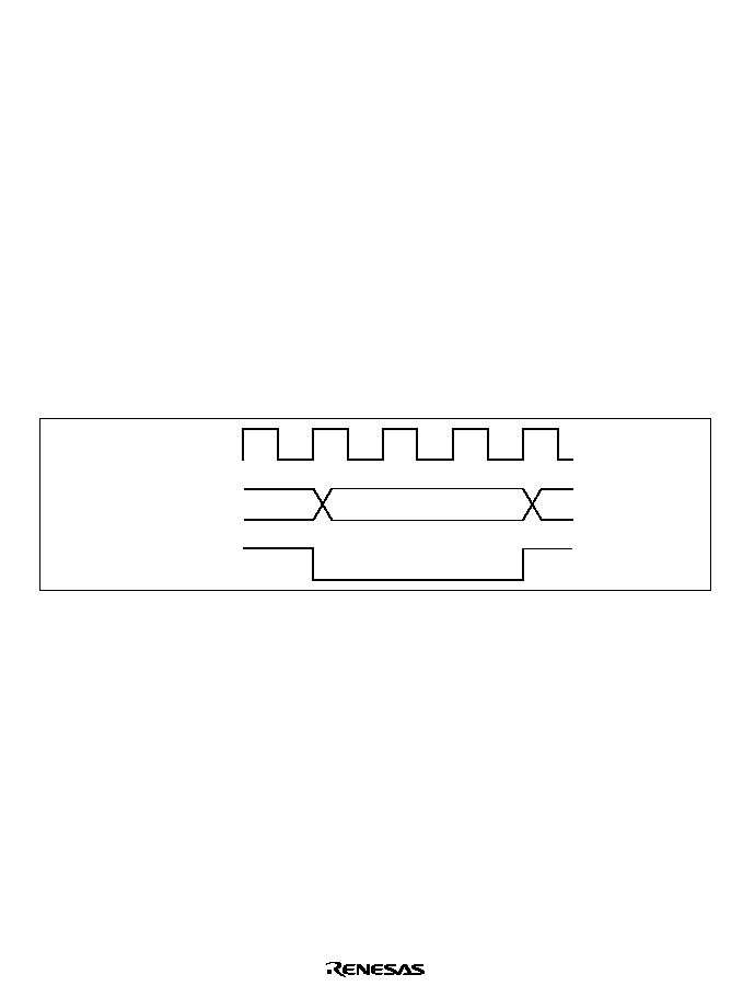
139
6.3.4
Chip Select Signals
For each of areas 0 to 7, the H8/3069F can output a chip select signal (
CS
0
to
CS
7
) that goes low
when the corresponding area is selected in expanded mode. Figure 6.4 shows the output timing of
a
CSn signal.
Output of
CS
0
to
CS
3
: Output of
CS
0
to
CS
3
is enabled or disabled in the data direction register
(DDR) of the corresponding port.
In the expanded modes with on-chip ROM disabled, a reset leaves pin
CS
0
in the output state and
pins
CS
1
to
CS
3
in the input state. To output chip select signals
CS
1
to
CS
3
, the corresponding
DDR bits must be set to 1. In the expanded modes with on-chip ROM enabled, a reset leaves pins
CS
0
to
CS
3
in the input state. To output chip select signals
CS
0
to
CS
3
, the corresponding DDR
bits must be set to 1. For details, see section 8, I/O Ports.
Output of
CS
4
to
CS
7
: Output of
CS
4
to
CS
7
is enabled or disabled in the chip select control
register (CSCR). A reset leaves pins
CS
4
to
CS
7
in the input state. To output chip select signals
CS
4
to
CS
7
, the corresponding CSCR bits must be set to 1. For details, see section 8, I/O Ports.
Address
External address in area n
CS
n
Figure 6.4
CSn Signal Output Timing (n = 0 to 7)
When the on-chip ROM, on-chip RAM, and on-chip registers are accessed,
CS
0
to
CS
7
remain
high. The
CS
n
signals are decoded from the address signals. They can be used as chip select
signals for SRAM and other devices.
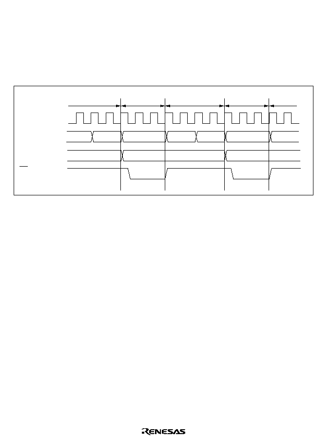
140
6.3.5
Address Output Method
The H8/3069F provides a choice of two address update methods: either the same method as in the
previous H8/300H Series (address update mode 1), or a method in which address update is
restricted to external space accesses or self-refresh cycles (address update mode 2).
Figure 6.5 shows examples of address output in these two update modes.
On-chip
memory cycle
On-chip
memory cycle
External
read cycle
On-chip
memory cycle
External
read cycle
Address update
mode 1
Address update
mode 2
RD
Figure 6.5 Sample Address Output in Each Address Update Mode
(Basic Bus Interface, 3-State Space)
Address Update Mode 1: Address update mode 1 is compatible with the previous H8/300H
Series. Addresses are always updated between bus cycles.
Address Update Mode 2: In address update mode 2, address updating is performed only in
external space accesses or self-refresh cycles. In this mode, the address can be retained between
an external space read cycle and an instruction fetch cycle (on-chip memory) by placing the
program in on-chip memory. Address update mode 2 is therefore useful when connecting a device
that requires address hold time with respect to the rise of the
RD strobe.
Switching between address update modes 1 and 2 is performed by means of the ADRCTL bit in
ADRCR. The initial value of ADRCR is the address update mode 1 setting, providing
compatibility with the previous H8/300H Series.
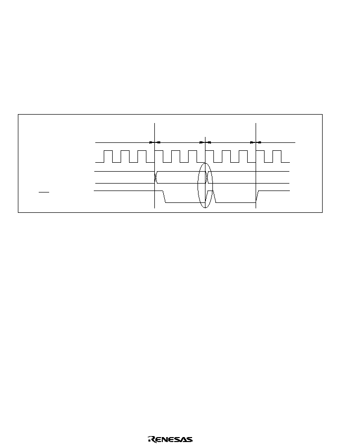
141
Cautions: When using address update modes, the following points should be noted.
�
When address update mode 2 is selected, the address in an internal space (on-chip memory or
internal I/O) access cycle is not output externally.
�
In order to secure address holding with respect to the rise of
RD, when address update mode 2
is used an external space read access must be completed within a single access cycle. For
example, in a word access to 8-bit access space, the bus cycle is split into two as shown in
figure 6.6, and so there is not a single access cycle. In this case, address holding is not
guaranteed at the rise of
RD between the first (even address) and second (odd address) access
cycles (area inside the ellipse in the figure).
On-chip
memory cycle
On-chip
memory cycle
External read cycle
(8-bit space word access)
Address update
mode 2
RD
Even address
Odd address
Figure 6.6 Example of Consecutive External Space Accesses in Address Update Mode 2
�
When address update mode 2 is selected, in a DRAM space CAS-before-RAS (CBR) refresh
cycle the previous address is retained (the area 2 start address is not output).
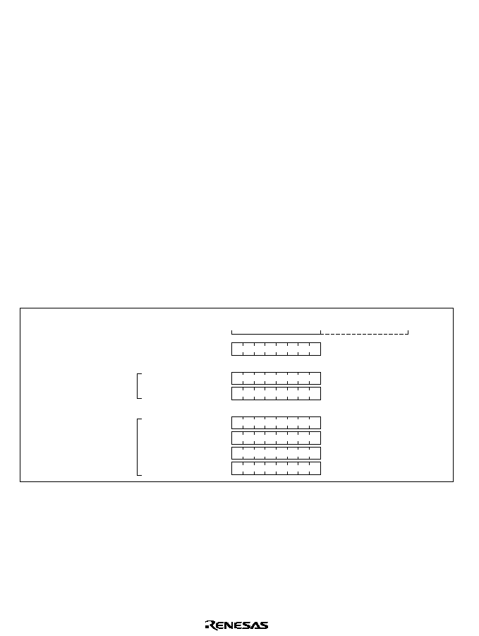
142
6.4
Basic Bus Interface
6.4.1
Overview
The basic bus interface enables direct connection of ROM, SRAM, and so on.
The bus specifications can be selected with ABWCR, ASTCR, WCRH, and WCRL
(see table 6.3).
6.4.2
Data Size and Data Alignment
Data sizes for the CPU and other internal bus masters are byte, word, and longword. The bus
controller has a data alignment function, and when accessing external space, controls whether the
upper data bus (D
15
to D
8
) or lower data bus (D
7
to D
0
) is used according to the bus specifications
for the area being accessed (8-bit access area or 16-bit access area) and the data size.
8-Bit Access Areas: Figure 6.7 illustrates data alignment control for 8-bit access space. With 8-
bit access space, the upper data bus (D
15
to D
8
) is always used for accesses. The amount of data
that can be accessed at one time is one byte: a word access is performed as two byte accesses, and
a longword access, as four byte accesses.
D
15
D
8
D
7
D
0
Upper data bus
Lower data bus
1st bus cycle
2nd bus cycle
1st bus cycle
2nd bus cycle
3rd bus cycle
4th bus cycle
Byte size
Word size
Longword size
Figure 6.7 Access Sizes and Data Alignment Control (8-Bit Access Area)
16-Bit Access Areas: Figure 6.8 illustrates data alignment control for 16-bit access areas. With
16-bit access areas, the upper data bus (D
15
to D
8
) and lower data bus (D
7
to D
0
) are used for
accesses. The amount of data that can be accessed at one time is one byte or one word, and a
longword access is executed as two word accesses.
143
In byte access, whether the upper or lower data bus is used is determined by whether the address is
even or odd. The upper data bus is used for an even address, and the lower data bus for an odd
address.
D
15
D
8
D
7
D
0
Upper data bus
Lower data bus
1st bus cycle
2nd bus cycle
Byte size
Longword size
� Even address
� Odd address
Word size
Byte size
Figure 6.8 Access Sizes and Data Alignment Control (16-Bit Access Area)
6.4.3
Valid Strobes
Table 6.4 shows the data buses used, and the valid strobes, for the access spaces.
In a read, the
RD signal is valid for both the upper and the lower half of the data bus.
In a write, the
HWR signal is valid for the upper half of the data bus, and the LWR signal for the
lower half.

144
Table 6.4
Data Buses Used and Valid Strobes
Area
Access
Size
Read/Write
Address
Valid Strobe
Upper Data Bus
(D
15
to D
8
)
Lower Data Bus
(D
7
to D
0
)
8-bit
Byte
Read
--
RD
Valid
Invalid
access
area
Write
--
HWR
Undetermined
data
16-bit
Byte
Read
Even
RD
Valid
Invalid
access
Odd
Invalid
Valid
area
Write
Even
HWR
Valid
Undetermined
data
Odd
LWR
Undetermined
data
Valid
Word
Read
--
RD
Valid
Valid
Write
--
HWR
,
LWR
Valid
Valid
Notes: 1. Undetermined data means that unpredictable data is output.
2. Invalid means that the bus is in the input state and the input is ignored.
6.4.4
Memory Areas
The initial state of each area is basic bus interface, three-state access space. The initial bus width
is selected according to the operating mode. The bus specifications described here cover basic
items only, and the following sections should be referred to for further details: Sections 6.4, Basic
Bus Interface, 6.5, DRAM Interface, and 6.8, Burst ROM Interface.
Area 0: Area 0 includes on-chip ROM, and in ROM-disabled expansion mode, all of area 0 is
external space. In ROM-enabled expansion mode, the space excluding on-chip ROM is external
space.
When area 0 external space is accessed, the
CS
0
signal can be output.
Either basic bus interface or burst ROM interface can be selected for area 0.
The size of area 0 is 128 kbytes in modes 1 and 2, and 2 Mbytes in modes 3, 4, and 5.
Areas 1 and 6: In external expansion mode, areas 1 and 6 are entirely external space.
When area 1 and 6 external space is accessed, the
CS
1
and
CS
6
pin signals respectively can be
output.
Only the basic bus interface can be used for areas 1 and 6.
The size of areas 1 and 6 is 128 kbytes in modes 1 and 2, and 2 Mbytes in modes 3, 4, and 5.

145
Areas 2 to 5: In external expansion mode, areas 2 to 5 are entirely external space.
When area 2 to 5 external space is accessed, signals
CS
2
to
CS
5
can be output.
Basic bus interface or DRAM interface can be selected for areas 2 to 5. With the DRAM
interface, signals
CS
2
to
CS
5
are used as
RAS signals.
The size of areas 2 to 5 is 128 kbytes in modes 1 and 2, and 2 Mbytes in modes 3, 4, and 5.
Area 7: Area 7 includes the on-chip RAM and registers. In external expansion mode, the space
excluding the on-chip RAM and registers is external space. The on-chip RAM is enabled when
the RAME bit in the system control register (SYSCR) is set to 1; when the RAME bit is cleared to
0, the on-chip RAM is disabled and the corresponding space becomes external space .
When area 7 external space is accessed, the
CS
7
signal can be output.
Only the basic bus interface can be used for the area 7 memory interface.
The size of area 7 is 128 kbytes in modes 1 and 2, and 2 Mbytes in modes 3, 4, and 5.
146
6.4.5
Basic Bus Control Signal Timing
8-Bit, Three-State-Access Areas
Figure 6.9 shows the timing of bus control signals for an 8-bit, three-state-access area. The upper
data bus (D
15
to D
8
) is used in accesses to these areas. The
LWR pin is always high. Wait states
can be inserted.
Bus cycle
External address in area n
Valid
Invalid
Valid
Undetermined data
High
Address bus
CS
n
AS
RD
D
15
to D
8
D
7
to D
0
HWR
LWR
D
15
to D
8
D
7
to D
0
Read access
Write access
Note: n = 7 to 0
T
1
T
2
T
3
Figure 6.9 Bus Control Signal Timing for 8-Bit, Three-State-Access Area
147
8-Bit, Two-State-Access Areas
Figure 6.10 shows the timing of bus control signals for an 8-bit, two-state-access area. The upper
data bus (D
15
to D
8
) is used in accesses to these areas. The
LWR pin is always high. Wait states
cannot be inserted.
Bus cycle
External address in area n
Valid
Invalid
Valid
Undetermined data
High
Address bus
CS
n
AS
RD
D
15
to D
8
D
7
to D
0
HWR
LWR
D
15
to D
8
D
7
to D
0
Read access
Write access
Note: n = 7 to 0
T
1
T
2
Figure 6.10 Bus Control Signal Timing for 8-Bit, Two-State-Access Area
148
16-Bit, Three-State-Access Areas
Figures 6.11 to 6.13 show the timing of bus control signals for a 16-bit, three-state-access area. In
these areas, the upper data bus (D
15
to D
8
) is used in accesses to even addresses and the lower data
bus (D
7
to D
0
) in accesses to odd addresses. Wait states can be inserted.
Bus cycle
Even external address in area n
Valid
Invalid
Valid
High
Address bus
CSn
AS
RD
D
15
to D
8
D
7
to D
0
HWR
LWR
D
15
to D
8
D
7
to D
0
Read access
Write access
Note: n = 7 to 0
T
1
T
2
T
3
Undetermined data
Figure 6.11 Bus Control Signal Timing for 16-Bit, Three-State-Access Area (1)
(Byte Access to Even Address)
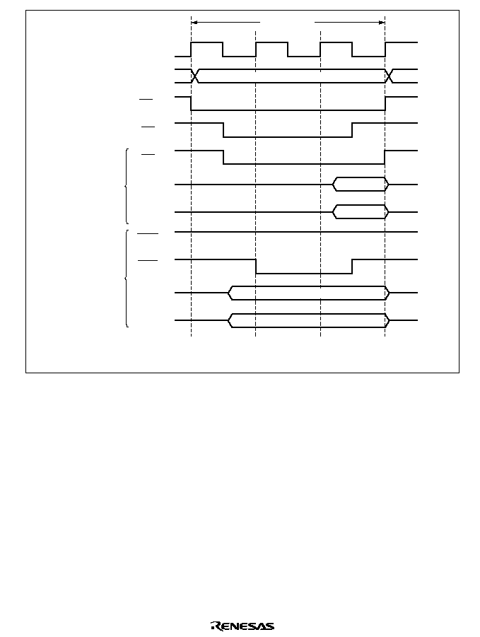
149
Bus cycle
Odd external address in area n
Valid
Invalid
Valid
Address bus
CS
n
AS
RD
D
15
to D
8
D
7
to D
0
HWR
LWR
D
15
to D
8
D
7
to D
0
Read access
Write access
Note: n = 7 to 0
T
1
T
2
T
3
High
Undetermined data
Figure 6.12 Bus Control Signal Timing for 16-Bit, Three-State-Access Area (2)
(Byte Access to Odd Address)
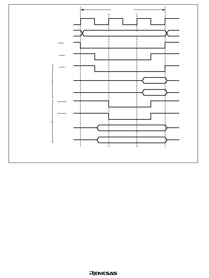
150
Bus cycle
External address in area n
Valid
Valid
Address bus
CS
n
AS
RD
D
15
to D
8
D
7
to D
0
HWR
LWR
D
15
to D
8
D
7
to D
0
Read access
Write access
Note: n = 7 to 0
T
1
T
2
T
3
Valid
Valid
Figure 6.13 Bus Control Signal Timing for 16-Bit, Three-State-Access Area (3)
(Word Access)
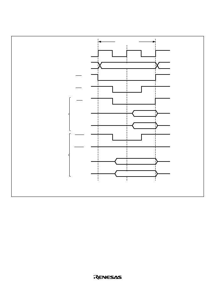
151
16-Bit, Two-State-Access Areas: Figures 6.14 to 6.16 show the timing of bus control signals for
a 16-bit, two-state-access area. In these areas, the upper data bus (D
15
to D
8
) is used in accesses to
even addresses and the lower data bus (D
7
to D
0
) in accesses to odd addresses. Wait states cannot
be inserted.
Bus cycle
Even external address in area n
Valid
Invalid
Valid
High
Address bus
CS
n
AS
RD
D
15
to D
8
D
7
to D
0
HWR
LWR
D
15
to D
8
D
7
to D
0
Read access
Write access
Note: n = 7 to 0
T
1
T
2
Undetermined data
Figure 6.14 Bus Control Signal Timing for 16-Bit, Two-State-Access Area (1)
(Byte Access to Even Address)
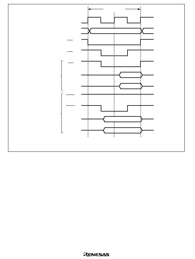
152
Bus cycle
Odd external address in area n
Valid
Invalid
Valid
High
Address bus
CS
n
AS
RD
D
15
to D
8
D
7
to D
0
HWR
LWR
D
15
to D
8
D
7
to D
0
Read access
Write access
Note: n = 7 to 0
T
1
T
2
Undetermined data
Figure 6.15 Bus Control Signal Timing for 16-Bit, Two-State-Access Area (2)
(Byte Access to Odd Address)
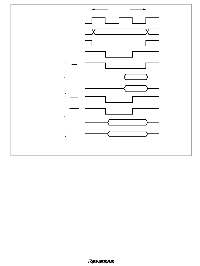
153
Bus cycle
External address in area n
Valid
Valid
Address bus
CS
n
AS
RD
D
15
to D
8
D
7
to D
0
HWR
LWR
D
15
to D
8
D
7
to D
0
Read access
Write access
Note: n = 7 to 0
T
1
T
2
Valid
Valid
Figure 6.16 Bus Control Signal Timing for 16-Bit, Two-State-Access Area (3)
(Word Access)
6.4.6
Wait Control
When accessing external space, the H8/3069F can extend the bus cycle by inserting one or more
wait states (T
w
). There are two ways of inserting wait states: (1) program wait insertion and (2)
pin wait insertion using the
WAIT pin.
Program Wait Insertion: From 0 to 3 wait states can be inserted automatically between the T
2
state and T
3
state on an individual area basis in three-state access space, according to the settings
of WCRH and WCRL.
Pin Wait Insertion: Setting the WAITE bit in BCR to 1 enables wait insertion by means of the
WAIT pin. When external space is accessed in this state, a program wait is first inserted. If the
WAIT pin is low at the falling edge of
in the last T
2
or T
W
state, another T
W
state is inserted. If
the
WAIT pin is held low, T
W
states are inserted until it goes high.
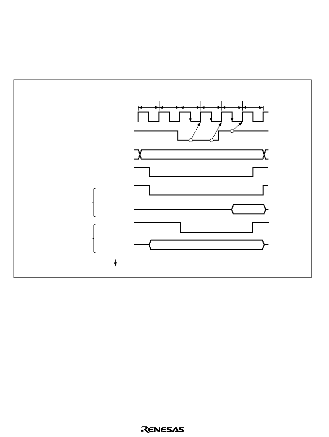
154
This is useful when inserting four or more T
W
states, or when changing the number of T
W
states for
different external devices.
The WAITE bit setting applies to all areas. Pin waits cannot be inserted in DRAM space.
Figure 6.17 shows an example of the timing for insertion of one program wait state in 3-state
space.
WAIT
Address bus
Data bus
Read access
Write access
Data bus
AS
RD
T
1
T
2
T
w
T
w
T
w
T
3
HWR
,
LWR
Note: indicates the timing of
WAIT
pin sampling.
Inserted
by program wait Inserted by
WAIT
pin
Read data
Write data
Figure 6.17 Example of Wait State Insertion Timing

155
6.5
DRAM Interface
6.5.1
Overview
The H8/3069F is provided with a DRAM interface with functions for DRAM control signal (
RAS,
UCAS, LCAS, WE) output, address multiplexing, and refreshing, that direct connection of
DRAM. In the expanded modes, external address space areas 2 to 5 can be designated as DRAM
space accessed via the DRAM interface. A data bus width of 8 or 16 bits can be selected for
DRAM space by means of a setting in ABWCR. When a 16-bit data bus width is selected, CAS is
used for byte access control. In the case of
�
16-bit organization DRAM, therefore, the 2-CAS
type can be connected. A fast page mode is supported in addition to the normal read and write
access modes.
6.5.2
DRAM Space and
RAS Output Pin Settings
Designation of areas 2 to 5 as DRAM space, and selection of the
RAS output pin for each area
designated as DRAM space, is performed by setting bits in DRCRA. Table 6.5 shows the
correspondence between the settings of bits DRAS2 to DRAS0 and the selected DRAM space and
RAS output pin.
When an arbitrary value has been set in DRAS2 to DRAS0, a write of a different value other than
000 must not be performed.

156
Table 6.5
Settings of Bits DRAS2 to DRAS0 and Corresponding DRAM Space (
RAS
Output Pin)
DRAS2 DRAS1 DRAS0 Area 5
Area 4
Area 3
Area 2
0
0
0
Normal space
Normal space
Normal space
Normal space
1
Normal space
Normal space
Normal space
DRAM space
(
CS
2
)
1
0
Normal space
Normal space
DRAM space
(
CS
3
)
DRAM space
(
CS
2
)
1
Normal space
Normal space
DRAM space
(
CS
2
)
*
DRAM space
(
CS
2
)
*
1
0
0
Normal space
DRAM space
(
CS
4
)
DRAM space
(
CS
3
)
DRAM space
(
CS
2
)
1
DRAM space
(
CS
5
)
DRAM space
(
CS
4
)
DRAM space
(
CS
3
)
DRAM space
(
CS
2
)
1
0
DRAM space
(
CS
4
)
*
DRAM space
(
CS
4
)
*
DRAM space
(
CS
2
)
*
DRAM space
(
CS
2
)
*
1
DRAM space
(
CS
2
)
*
DRAM space
(
CS
2
)
*
DRAM space
(
CS
2
)
*
DRAM space
(
CS
2
)
*
Note:
*
A single
CS
n
pin serves as a common
RAS
output pin for a number of areas. Unused
CS
n
pins can be used as input/output ports.
6.5.3
Address Multiplexing
When DRAM space is accessed, the row address and column address are multiplexed. The
address multiplexing method is selected with bits MXC1 and MXC0 in DRCRB according to the
number of bits in the DRAM column address. Table 6.6 shows the correspondence between the
settings of MXC1 and MXC0 and the address multiplexing method.

157
Table 6.6
Settings of Bits MXC1 and MXC0 and Address Multiplexing Method
DRCRB
Column
Address
Address Pins
MXC1 MXC0 Bits
A
23
to A
13
A
12
A
11
A
10
A
9
A
8
A
7
A
6
A
5
A
4
A
3
A
2
A
1
A
0
Row
address
0
0
8 bits
A
23
to A
13
A
20
*
A
19
A
18
A
17
A
16
A
15
A
14
A
13
A
12
A
11
A
10
A
9
A
8
1
9 bits
A
23
to A
13
A
12
A
20
*
A
19
A
18
A
17
A
16
A
15
A
14
A
13
A
12
A
11
A
10
A
9
1
0
10 bits
A
23
to A
13
A
12
A
11
A
20
*
A
19
A
18
A
17
A
16
A
15
A
14
A
13
A
12
A
11
A
10
1
Illegal
setting
--
--
--
--
--
--
--
--
--
--
--
--
--
--
Column
address
--
--
--
A
23
to A
13
A
12
A
11
A
10
A
9
A
8
A
7
A
6
A
5
A
4
A
3
A
2
A
1
A
0
Note:
*
Row address bit A
20
is not multiplexed in 1-Mbyte mode.
6.5.4
Data Bus
If the bit in ABWCR corresponding to an area designated as DRAM space is set to 1, that area is
designated as 8-bit DRAM space; if the bit is cleared to 0, the area is designated as 16-bit DRAM
space. In 16-bit DRAM space,
�
16-bit organization DRAM can be connected directly.
In 8-bit DRAM space the upper half of the data bus, D
15
to D
8
, is enabled, while in 16-bit DRAM
space both the upper and lower halves of the data bus, D
15
to D
0
, are enabled.
Access sizes and data alignment are the same as for the basic bus interface: see section 6.4.2, Data
Size and Data Alignment.
6.5.5
Pins Used for DRAM Interface
Table 6.7 shows the pins used for DRAM interfacing and their functions.

158
Table 6.7
DRAM Interface Pins
Pin
With DRAM
Designated Name
I/O
Function
PB4
UCAS
Upper column
address strobe
Output
Upper column address strobe for DRAM
space access (when CSEL = 0 in DRCRB)
PB5
LCAS
Lower column
address strobe
Output
Lower column address strobe for DRAM
space access (when CSEL = 0 in DRCRB)
HWR
UCAS
Upper column
address strobe
Output
Upper column address strobe for DRAM
space access (when CSEL = 1 in DRCRB)
LWR
LCAS
Lower column
address strobe
Output
Lower column address strobe for DRAM
space access (when CSEL = 1 in DRCRB)
CS
2
RAS
2
Row address
strobe 2
Output
Row address strobe for DRAM space
access
CS
3
RAS
3
Row address
strobe 3
Output
Row address strobe for DRAM space
access
CS
4
RAS
4
Row address
strobe 4
Output
Row address strobe for DRAM space
access
CS
5
RAS
5
Row address
strobe 5
Output
Row address strobe for DRAM space
access
RD
WE
Write enable
Output
Write enable for DRAM space write
access
*
P80
RFSH
Refresh
Output
Goes low in refresh cycle
A
12
to A
0
A
12
to A
0
Address
Output
Row address/column address multiplexed
output
D
15
to D
0
D
15
to D
0
Data
I/O
Data input/output pins
Note:
*
Fixed high in a read access.
6.5.6
Basic Timing
Figure 6.18 shows the basic access timing for DRAM space. The basic DRAM access timing is
four states: one precharge cycle (T
p
) state, one row address output cycle (T
r
) state, and two column
address output cycle (T
c1
, T
c2
) states. Unlike the basic bus interface, the corresponding bits in
ASTCR control only enabling or disabling of wait insertion between T
c1
and T
c2
, and do not affect
the number of access states. When the corresponding bit in ASTCR is cleared to 0, wait states
cannot be inserted between T
c1
and T
c2
in the DRAM access cycle.
If a DRAM read/write cycle is followed by an access cycle for an external area other than DRAM
space when
HWR and LWR are selected as the UCAS and LCAS output pins, an idle cycle (Ti) is
inserted unconditionally immediately after the DRAM access cycle. See section 6.9, Idle Cycle,
for details.
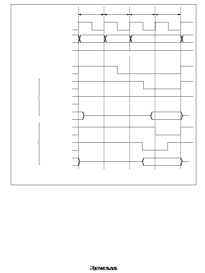
159
A
23
to A
0
CSn
(
RAS
)
T
p
Tr
T
c1
T
c2
(UCAS
/
LCAS
)
PB
4
/PB
5
AS
RD
(
WE
)
D
15
to D
0
RD
(
WE
)
D
15
to D
0
(
UCAS
/
LCAS
)
PB
4
/PB
5
Row
Column
Read access
Write access
Note: n = 2 to 5
High level
High level
Figure 6.18 Basic Access Timing (CSEL = 0 in DRCRB)
6.5.7
Precharge State Control
In the H8/3069F, provision is made for the DRAM RAS precharge time by always inserting one
RAS precharge state (T
p
) when DRAM space is accessed. This can be changed to two T
p
states by
setting the TPC bit to 1 in DRCRB. The optimum number of T
p
cycles should be set according to
the DRAM connected and the operating frequency of the H8/3069F chip. Figure 6.19 shows the
timing when two T
p
states are inserted.
When the TCP bit is set to 1, two T
p
states are also used for CAS-before-RAS refresh cycles.
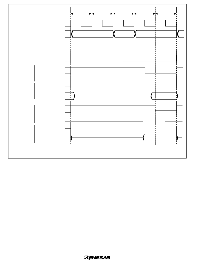
160
A
23
to A
0
CSn
(
RAS
)
AS
T
p1
Tr
T
c1
(
UCAS
/
LCAS
)
PB
4
/PB
5
RD
(
WE
)
D
15
to D
0
RD
(
WE
)
D
15 to
D
0
(
UCAS
/
LCAS
)
PB
4
/PB
5
T
c2
T
p2
Note: n = 2 to 5
Row
High level
High level
Column
Read access
Write access
Figure 6.19 Timing with Two Precharge States (CSEL = 0 in DRCRB)
6.5.8
Wait Control
In a DRAM access cycle, wait states can be inserted (1) between the T
r
state and T
c1
state, and (2)
between the T
c1
state and T
c2
state.
Insertion of T
rw
Wait State between T
r
and T
c1
: One T
rw
state can be inserted between T
r
and
T
c1
by setting the RCW bit to 1 in DRCRB.
Insertion of T
w
Wait State(s) between T
c1
and T
c2
: When the bit in ASTCR corresponding to an
area designated as DRAM space is set to 1, from 0 to 3 wait states can be inserted between the T
c1
state and T
c2
state by means of settings in WCRH and WCRL.
Figure 6.20 shows an example of the timing for wait state insertion.
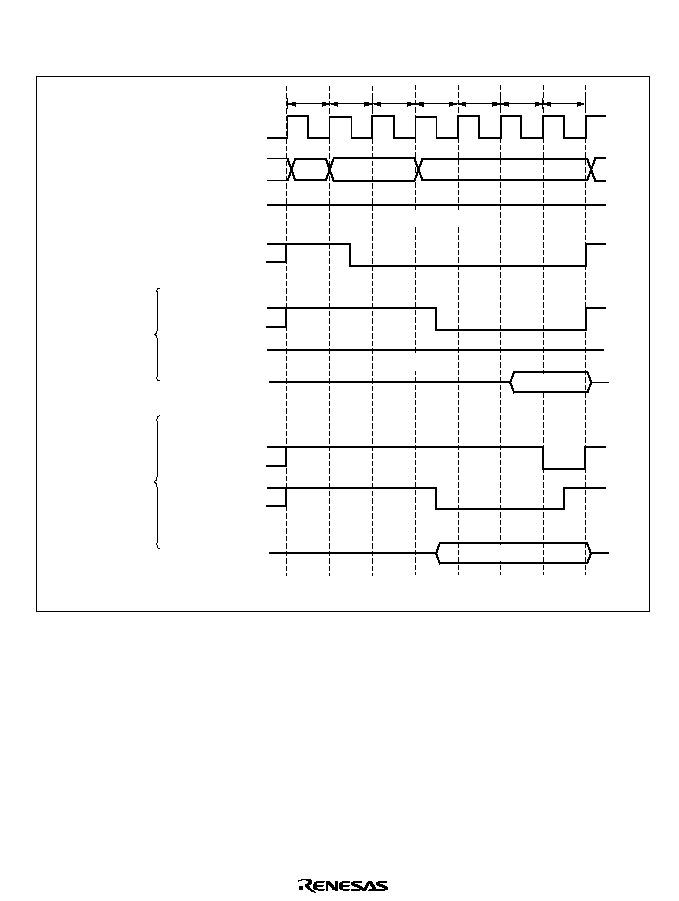
161
The settings of the RCW bit in DRCRB and of ASTCR, WCRH, and WCRL do not affect refresh
cycles. Wait states cannot be inserted in a DRAM space access cycle by means of the
WAIT pin.
T
p
Tr
T
c1
T
c2
(
UCAS
/
LCAS
)
PB
4
/PB
5
RD
(
WE
)
CSn
(
RAS
)
AS
D
15
to D
0
RD
(
WE
)
D
15
to D
0
(
UCAS
/
LCAS
)
PB
4
/PB
5
A
23
to A
0
Trw
Tw
Tw
Write access
Read access
Read data
Write data
Note: n = 2 to 5
Row
Column
High level
High level
Figure 6.20 Example of Wait State Insertion Timing (CSEL = 0)
6.5.9
Byte Access Control and
CAS Output Pin
When an access is made to DRAM space designated as a 16-bit-access area in ABWCR, column
address strobes (
UCAS and LCAS) corresponding to the upper and lower halves of the external
data bus are output. In the case of
�
16-bit organization DRAM, the 2-CAS type can be
connected.
Either PB4 and PB5, or
HWR and LWR, can be used as the UCAS and LCAS output pins, the
selection being made with the CSEL bit in DRCRB. Table 6.8 shows the CSEL bit settings and
corresponding output pin selections.
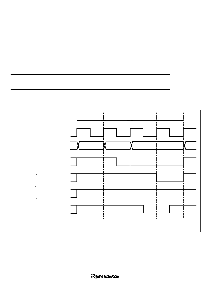
162
When an access is made to DRAM space designated as an 8-bit-access area in ABWCR, only
UCAS is output. When the entire DRAM space is designated as 8-bit-access space and CSEL = 0,
PB5 can be used as an input/output port.
Note that
RAS down mode cannot be used when a device other than DRAM is connected to
external space and
HWR and LWR are used as write strobes. In this case, also, an idle cycle (Ti)
is always inserted when an external access to other than DRAM space occurs after a DRAM space
access. For details, see section 6.9, Idle Cycle.
Table 6.8
CSEL Settings and
UCAS and LCAS Output Pins
CSEL
UCAS
LCAS
0
PB
4
PB
5
1
HWR
LWR
Figure 6.21 shows the control timing.
A
23
to A
0
CSn
(
RAS
)
T
p
Tr
T
c1
T
c2
PB
4
(
UCAS
)
PB
5
(
LCAS
)
RD
(
WE
)
Note: n = 2 to 5
Byte control
Row
Column
Figure 6.21 Control Timing (Upper-Byte Write Access When CSEL = 0)
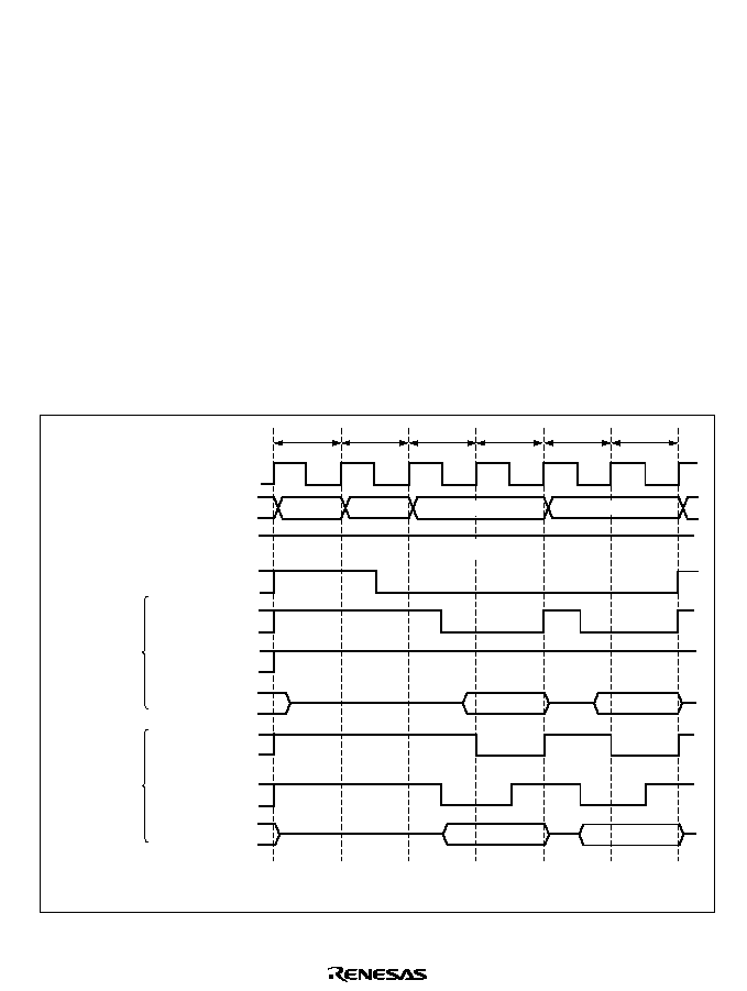
163
6.5.10 Burst
Operation
With DRAM, in addition to full access (normal access) in which data is accessed by outputting a
row address for each access, a fast page mode is also provided which can be used when making a
number of consecutive accesses to the same row address. This mode enables fast (burst) access of
data by simply changing the column address after the row address has been output. Burst access
can be selected by setting the BE bit to 1 in DRCRA.
Burst Access (Fast Page Mode) Operation Timing: Figure 6.22 shows the operation timing for
burst access. When there are consecutive access cycles for DRAM space, the column address and
CAS signal output cycles (two states) continue as long as the row address is the same for
consecutive access cycles. In burst access, too, the bus cycle can be extended by inserting wait
states between T
c1
and T
c2
. The wait state insertion method and timing are the same as for full
access: see section 6.5.8, Wait Control, for details.
The row address used for the comparison is determined by the bus width of the relevant area set in
bits MXC1 and MXC0 in DRCRB, and in ABWCR. Table 6.9 shows the compared row addresses
corresponding to the various settings of bits MXC1 and MXC0, and ABWCR.
A
23
to A
0
CS
n(
RAS
)
AS
T
p
Tr
T
c2
(
UCAS
/
LCAS
)
PB
4
/PB
5
RD
(
WE
)
D
15
to D
0
(
UCAS
/
LCAS
)
PB
4
/PB
5
T
c2
T
c1
T
c1
D
15
to D
0
RD
(
WE
)
Note: n = 2 to 5
Read access
Write access
Row
Column 1
Column 2
High level
Figure 6.22 Operation Timing in Fast Page Mode

164
Table 6.9
Correspondence between Settings of MXC1 and MXC0 Bits and ABWCR, and
Row Address Compared in Burst Access
DRCRB
ABWCR
Operating Mode
MXC1
MXC0
ABWn
Bus Width
Compared Row Address
Modes 1 and 2
0
0
0
16 bits
A19 to A9
(1-Mbyte)
1
8 bits
A19 to A8
1
0
16 bits
A19 to A10
1
8 bits
A19 to A9
1
0
0
16 bits
A19 to A11
1
8 bits
A19 to A10
1
--
--
Illegal setting
Modes 3, 4, and 5
0
0
0
16 bits
A23 to A9
(16-Mbyte)
1
8 bits
A23 to A8
1
0
16 bits
A23 to A10
1
8 bits
A23 to A9
1
0
0
16 bits
A23 to A11
1
8 bits
A23 to A10
1
--
--
Illegal setting
Note:
n = 2 to 5
RAS Down Mode and RAS Up Mode: With DRAM provided with fast page mode, as long as
accesses are to the same row address, burst operation can be continued without interruption even if
accesses are not consecutive by holding the
RAS signal low.
�
RAS Down Mode
To select RAS down mode, set the BE and RDM bits to 1 in DRCRA. If access to DRAM
space is interrupted and another space is accessed, the
RAS signal is held low during the access
to the other space, and burst access is performed if the row address of the next DRAM space
access is the same as the row address of the previous DRAM space access. Figure 6.23 shows
an example of the timing in RAS down mode.
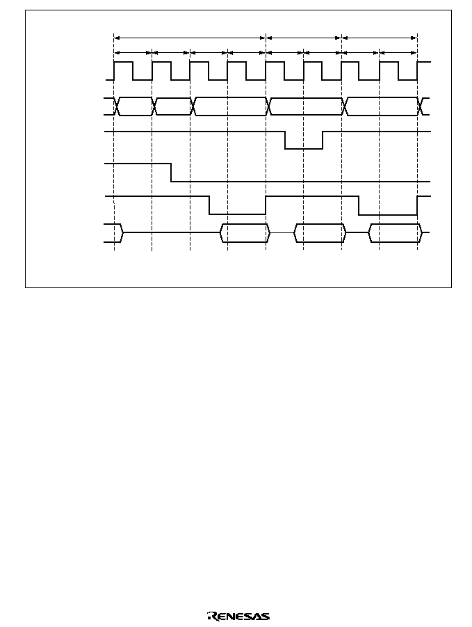
165
A
23
to A
0
CSn
(
RAS
)
T
p
Tr
T
c2
(
UCAS
/
LCAS
)
PB
4
/PB
5
D
15
to D
0
T
2
T
c1
T
1
T
c2
T
c1
AS
Note: n = 2 to 5
DRAM access
DRAM access
External space
access
Figure 6.23 Example of Operation Timing in RAS Down Mode (CSEL = 0)
When RAS down mode is selected, the conditions for an asserted
RASn signal to return to the
high level are as shown below. The timing in these cases is shown in figure 6.24.
When DRAM space with a different row address is accessed
Immediately before a CAS-before-RAS refresh cycle
When the BE bit or RDM bit is cleared to 0 in DRCRA
Immediately before release of the external bus
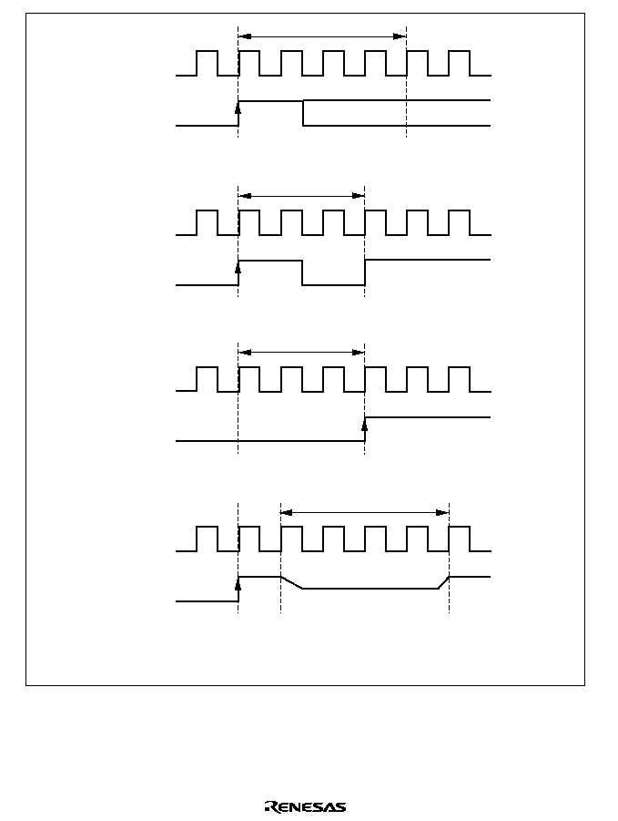
166
RAS
n
RAS
n
RAS
n
RAS
n
Note: n = 2 to 5
DRAM access cycle
CBR refresh cycle
DRCRA write cycle
External bus released
High-impedance
(a) Access to DRAM space with a different row address
(b) CAS-before-RAS refresh cycle
(c) BE bit or RDM bit cleared to 0 in DRCRA
(d) External bus released
Figure 6.24
RASn Negation Timing when RAS Down Mode is Selected
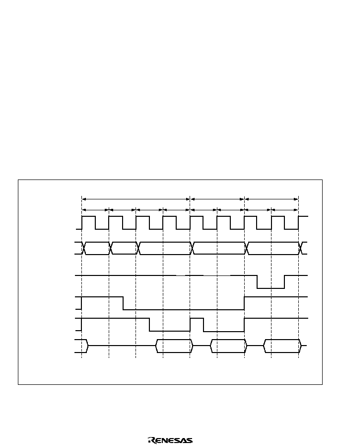
167
When RAS down mode is selected, the CAS-before-RAS refresh function provided with this
DRAM interface must always be used as the DRAM refreshing method. When a refresh
operation is performed, the
RAS signal goes high immediately beforehand. The refresh
interval setting must be made so that the maximum DRAM
RAS pulse width specification is
observed.
When the self-refresh function is used, the RDM bit must be cleared to 0, and RAS up mode
selected, before executing a SLEEP instruction in order to enter software standby mode.
Select RAS down mode again after exiting software standby mode.
Note that RAS down mode cannot be used when
HWR and LWR are selected for UCAS and
LCAS, a device other than DRAM is connected to external space, and HWR and LWR are
used as write strobes.
�
RAS Up Mode
To select RAS up mode, clear the RDM bit to 0 in DRCRA. Each time access to DRAM space
is interrupted and another space is accessed, the
RAS signal returns to the high level. Burst
operation is only performed if DRAM space is continuous. Figure 6.25 shows an example of
the timing in RAS up mode.
A
23
to A
0
CSn
(
RAS
)
AS
T
p
Tr
T
c2
D
15
to D
0
T
2
T
c1
T
1
T
c2
T
c1
PB
4
/PB
5
(
UCAS
/
LCAS
)
Note: n = 2 to 5
DRAM access
DRAM access
External space
access
Figure 6.25 Example of Operation Timing in RAS Up Mode
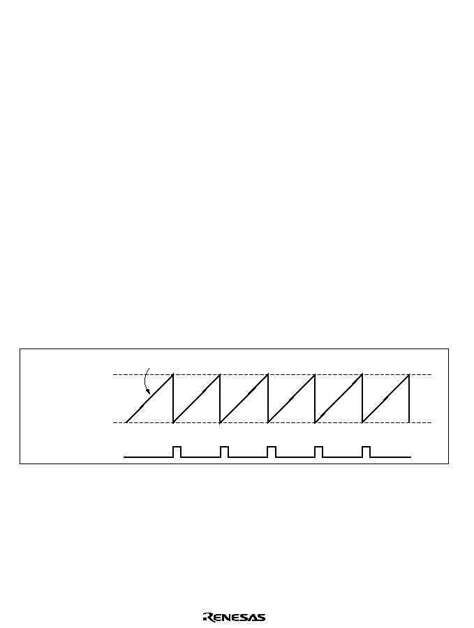
168
6.5.11
Refresh Control
The H8/3069F is provided with a CAS-before-RAS (CBR) function and self-refresh function as
DRAM refresh control functions.
CAS-Before-RAS (CBR) Refreshing: To select CBR refreshing, set the RCYCE bit to 1 in
DRCRB.
With CBR refreshing, RTCNT counts up using the input clock selected by bits CKS2 to CKS0 in
RTMCSR, and a refresh request is generated when the count matches the value set in RTCOR
(compare match). At the same time, RTCNT is reset and starts counting up again from H'00.
Refreshing is thus repeated at fixed intervals determined by RTCOR and bits CKS2 to CKS0. A
refresh cycle is executed after this refresh request has been accepted and the DRAM interface has
acquired the bus. Set a value in bits CKS2 to CKS0 in RTCOR that will meet the refresh interval
specification for the DRAM used. When RAS down mode is used, set the refresh interval so that
the maximum
RAS pulse width specification is met.
RTCNT starts counting up when bits CKS2 to CKS0 are set. RTCNT and RTCOR settings should
therefore be completed before setting bits CKS2 to CKS0.
Also note that a repeat refresh request generated during a bus request, or a refresh request during
refresh cycle execution, will be ignored.
RTCNT operation is shown in figure 6.26, compare match timing in figure 6.27, and CBR refresh
timing in figures 6.28 and 6.29.
RTCNT
RTCOR
H'00
Refresh request
Figure 6.26 RTCNT Operation
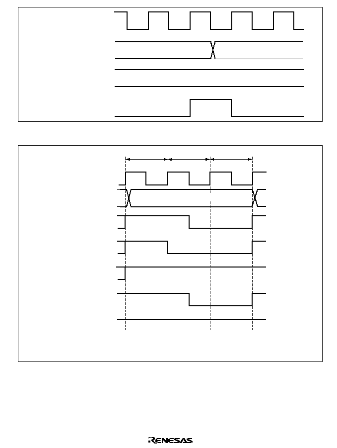
169
N
N
H'00
RTCNT
RTCOR
Refresh request signal
and CMF bit setting signal
Figure 6.27 Compare Match Timing
T
Rp
T
R1
T
R2
CS
n
(
RAS
)
(
UCAS
/
LCAS
)
PB
4
/PB
5
RD
(
WE
)
RFSH
AS
Address bus
*
Area 2 start address
High
High level
Note:
*
In address update mode 1, the area 2 start address is output.
In address update mode 2, the address in the preceding bus cycle is retained.
Figure 6.28 CBR Refresh Timing (CSEL = 0, TPC = 0, RLW = 0)
The basic CBS refresh cycle timing comprises three states: one RAS precharge cycle (T
RP
) state,
and two RAS output cycle (T
R1
, T
R2
) states. Either one or two states can be selected for the RAS
precharge cycle. When the TPC bit is set to 1 in DRCRB,
RAS signal output is delayed by one
cycle. This does not affect the timing of
UCAS and LCAS output.
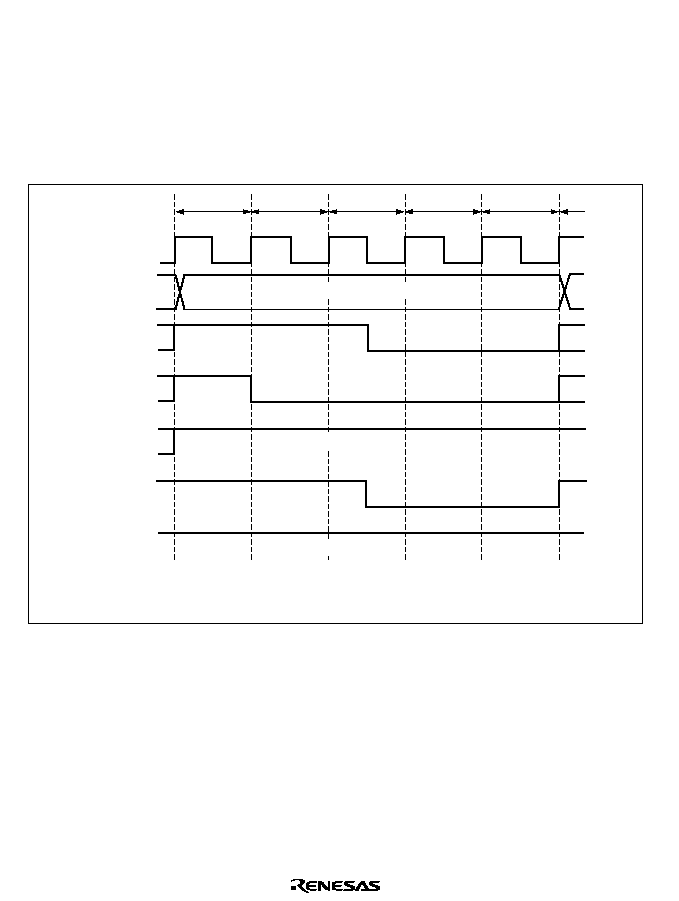
170
Use the RLW bit in DRCRB to adjust the
RAS signal width. A single refresh wait state (T
RW
) can
be inserted between the T
R1
state and T
R2
state by setting the RLW bit to 1.
The RLW bit setting is valid only for CBR refresh cycles, and does not affect DRAM read/write
cycles. The number of states in the CBR refresh cycle is not affected by the settings in ASTCR,
WCRH, or WCRL, or by the state of the
WAIT pin.
Figure 6.29 shows the timing when the TPC bit and RLW bit are both set to 1.
T
Rp1
T
RP2
T
R1
T
RW
RD
(
WE
)
CS
n
(
RAS
)
(
UCAS
/
LCAS
)
PB
4
/PB
5
T
R2
RFSH
AS
Address bus
*
Area 2 start address
High
High level
Note:
*
In address update mode 1, the area 2 start address is output.
In address update mode 2, the address in the preceding bus cycle is retained.
Figure 6.29 CBR Refresh Timing (CSEL = 0, TPC = 1, RLW = 1)
DRAM must be refreshed immediately after powering on in order to stabilize its internal state.
When using the H8/3069F CAS-before-RAS refresh function, therefore, a DRAM stabilization
period should be provided by means of interrupts by another timer module, or by counting the
number of times bit 7 (CMF) of RTMCSR is set, for instance, immediately after bits DRAS2 to
DRAS0 have been set in DRCRA.
Self-Refreshing: A self-refresh mode (battery backup mode) is provided for DRAM as a kind of
standby mode. In this mode, refresh timing and refresh addresses are generated within the
DRAM. The H8/3069F has a function that places the DRAM in self-refresh mode when the chip
enters software standby mode.
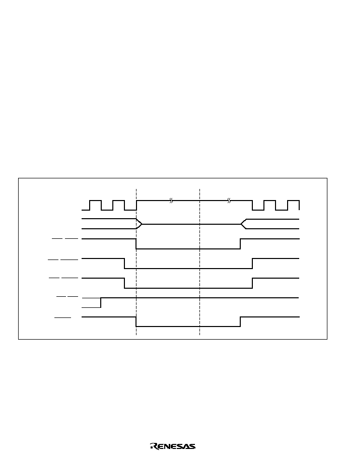
171
To use the self-refresh function, set the SRFMD bit to 1 in DRCRA. When a SLEEP instruction is
subsequently executed in order to enter software standby mode, the
CAS and RAS signals are
output and the DRAM enters self-refresh mode, as shown in figure 6.30.
When the chip exits software standby mode,
CAS and RAS outputs go high.
The following conditions must be observed when the self-refresh function is used:
�
When burst access is selected, RAS up mode must be selected before executing a SLEEP
instruction in order to enter software standby mode. Therefore, if RAS down mode has been
selected, the RDM bit in DRCRA must be cleared to 0 and RAS up mode selected before
executing the SLEEP instruction. Select RAS down mode again after exiting software standby
mode.
�
The instruction immediately following a SLEEP instruction must not be located in an area
designated as DRAM space.
The self-refresh function will not work properly unless the above conditions are observed.
CS
n
(RAS)
Address bus
PB
4
(UCAS)
PB
5
(LCAS)
RD(WE)
RFSH
Software standby
mode
Oscillation stabilization
time
High-impedance
Figure 6.30 Self-Refresh Timing (CSEL = 0)
Refresh Signal (
RFSH): A refresh signal (RFSH) that transmits a refresh cycle off-chip can be
output by setting the RFSHE bit to 1 in DRCRA.
RFSH output timing is shown in figures 6.28,
6.29, and 6.30.

172
6.5.12
Examples of Use
Examples of DRAM connection and program setup procedures are shown below. When the
DRAM interface is used, check the DRAM device characteristics and choose the most appropriate
method of use for that device.
Connection Examples
�
Figure 6.31 shows typical interconnections when using two 2-CAS type 16-Mbit DRAMs
using a
�
16-bit organization, and the corresponding address map. The DRAMs used in this
example are of the 10-bit row address
�
10-bit column address type. Up to four DRAMs can
be connected by designating areas 2 to 5 as DRAM space.
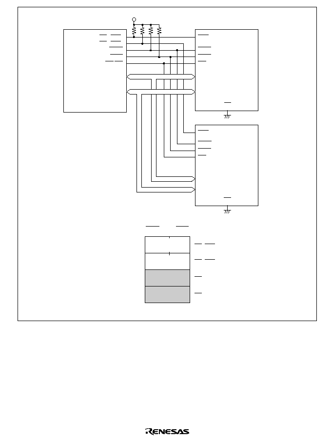
173
CS
2
(RAS
2
)
CS
3
(RAS
3
)
RD (WE)
A
10
-A
1
D
15
-D
0
A
9
-A
0
D
15
-D
0
PB
4
(UCAS)
PB
5
(LCAS)
RAS
WE
UCAS
LCAS
A
9
-A
0
D
15
-D
0
RAS
WE
UCAS
LCAS
No.1
No.2
OE
OE
DRAM (No.1)
H'400000
H'5FFFFE
H'600000
H'7FFFFE
H'800000
H'9FFFFE
H'A00000
H'BFFFFE
DRAM (No.2)
Normal
Normal
CS
2
(RAS
2
)
CS
3
(RAS
3
)
CS
4
CS
5
PB
4
(UCAS)
PB
5
(LCAS)
15
0
7
8
H8/3069F
2-CAS 16-Mbit DRAM
10-bit row address x 10-bit column address
x16-bit organization
(a) Interconnections (example)
(b) Address map
Area 2
Area 3
Area 4
Area 5
Figure 6.31 Interconnections and Address Map for 2-CAS 16-Mbit DRAMs with
�
16-
Bit Organization
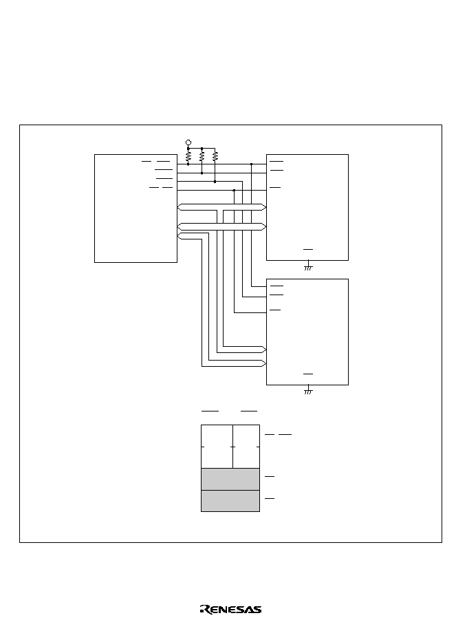
174
�
Figure 6.32 shows typical interconnections when using two 16-Mbit DRAMs using a
�
8-bit
organization, and the corresponding address map. The DRAMs used in this example are of the
11-bit row address
�
10-bit column address type. The
CS
2
pin is used as the common
RAS
output pin for areas 2 and 3. When the
DRAM address space spans a number of contiguous
areas, as in this example, the appropriate setting of bits DRAS2 to DRAS0 enables a single
CS
pin to be used as the common
RAS output pin for a number of areas, and makes it possible to
directly connect large-capacity DRAM with address space that spans a maximum of four areas.
Any unused
CS pins (in this example, the CS
3
pin) can be used as input/output ports.
CS
2
(RAS
2
)
RD (WE)
A
21
, A
10
-A
1
D
15
-D
8
D
7
-D
0
A
10
-A
0
D
7
-D
0
PB
4
(UCAS)
PB
5
(LCAS)
RAS
WE
CAS
A
10
-A
0
D
7
-D
0
RAS
WE
CAS
No.1
No.2
OE
OE
DRAM
(No.1)
H'400000
H'5FFFFE
H'600000
H'7FFFFE
H'800000
H'9FFFFE
H'A00000
H'BFFFFE
DRAM
(No.2)
CS
2
(RAS
2
)
CS
4
CS
5
PB
4
(UCAS)
PB
5
(LCAS)
15
0
7
8
H8/3069F
2-CAS 16-Mbit DRAM
11-bit row address x 10-bit column address
x8-bit organization
(a) Interconnections (example)
(b) Address map
16-Mbyte mode
Area 2
Area 3
Area 4
Area 5
Normal
Normal
Figure 6.32 Interconnections and Address Map for 16-Mbit DRAMs with
�
8-Bit
Organization
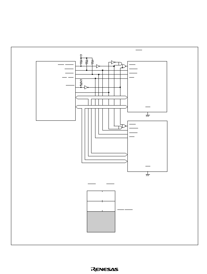
175
�
Figure 6.33 shows typical interconnections when using two 4-Mbit DRAMs, and the
corresponding address map. The DRAMs used in this example are of the 9-bit row address
�
9-bit column address type. In this example, upper address decoding allows multiple DRAMs
to be connected to a single area. The
RFSH pin is used in this case, since both DRAMs must
be refreshed simultaneously. However, note that RAS down mode cannot be used in this
interconnection example.
CS
2
(RAS
2
)
RD (WE)
A
9
-A
1
D
15
-D
0
A
8
-A
0
D
15
-D
0
PB
4
(UCAS)
PB
5
(LCAS)
RAS
WE
UCAS
LCAS
A
8
-A
0
D
15
-D
0
RAS
WE
UCAS
LCAS
No.1
No.2
OE
OE
DRAM (No.1)
H'400000
H'47FFFE
H'480000
H'4FFFFE
H'500000
H'5FFFFE
DRAM (No.2)
Not used
(a) Interconnections (example)
CS
2
(RAS
2
)
PB
4
(UCAS)
PB
5
(LCAS)
15
0
7
8
Area 2
16-Mbyte mode
(b) Address map
H8/3069F
2-CAS 4-Mbit DRAM
9-bit row address x 9-bit column address
x16-bit organization
RFSH
A
19
Figure 6.33 Interconnections and Address Map for 2-CAS 4-Mbit DRAMs with
�
16-Bit
Organization
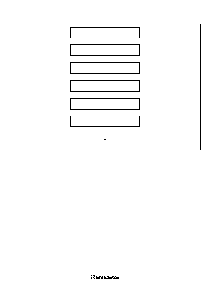
176
Example of Program Setup Procedure: Figure 6.34 shows an example of the program setup
procedure.
Set ABWCR
Set RTCOR
Set bits CKS2 to CKS0 in RTMCSR
Set DRCRB
Set DRCRA
Wait for DRAM stabilization time
DRAM can be accessed
Figure 6.34 Example of Setup Procedure when Using DRAM Interface
6.5.13
Usage Notes
Note the following points when using the DRAM refresh function.
�
Refresh cycles will not be executed when the external bus released state, software standby
mode, or a bus cycle is extended by means of wait state insertion. Refreshing must therefore
be performed by other means in these cases.
�
If a refresh request is generated internally while the external bus is released, the first request is
retained and a single refresh cycle will be executed after the bus-released state is cleared.
Figure 6.35 shows the bus cycle in this case.
�
When a bus cycle is extended by means of wait state insertion, the first request is retained in
the same way as when the external bus has been released.
�
In the event of contention with a bus request from an external bus master when a transition is
made to software standby mode, the
BACK and strobe states may be indeterminate after the
transition to software standby mode (see figure 6.36).
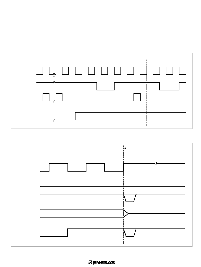
177
When software standby mode is used, the BRLE bit should be cleared to 0 in BRCR before
executing the SLEEP instruction.
Similar contention in a transition to self-refresh mode may prevent dependable strobe
waveform output. This can also be avoided by clearing the BRLE bit to 0 in BRCR.
�
Immediately after self-refreshing is cleared, external bus release is possible during a given
period until the start of a CPU cycle. Attention must be paid to the
RAS state to ensure that the
specification for the
RAS precharge time immediately after self-refreshing is met.
RFSH
Refresh
request
BACK
External bus released
Refresh cycle
CPU cycle
Refresh cycle
Figure 6.35 Bus-Released State and Refresh Cycles
,,,,,,,,
,,,,,,,,
,,,,,,,,
,,,,,,,,
,,,,,,,,
,,,,,,,,
BREQ
BACK
Software standby mode
Address bus
Strobe
,,,,,,,,
,,,,,,,,
,,,,,,,,
,,,,,,,,
,,,,,,,,
Figure 6.36 Bus-Released State and Software Standby Mode
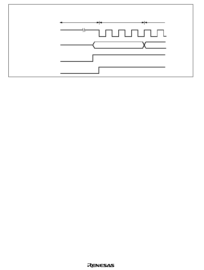
178
@SP
RAS
CAS
Oscillation stabilization
time on exit from software
standby mode
CPU internal cycle
(period in which external
bus can be released)
CPU cycle
Address
Figure 6.37 Self-Refresh Clearing
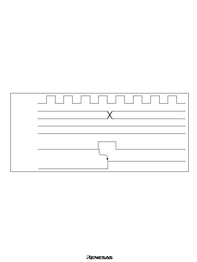
179
6.6
Interval Timer
6.6.1
Operation
When DRAM is not connected to the H8/3069F chip, the refresh timer can be used as an interval
timer by clearing bits DRAS2 to DRAS0 in DRCRA to 0. After setting RTCOR, selection a clock
source with bits CKS2 to CKS0 in RTMCSR, and set the CMIE bit to 1.
Timing of Setting of Compare Match Flag and Clearing by Compare Match: The CMF flag
in RTMCSR is set to 1 by a compare match output when the RTCOR and RTCNT values match.
The compare match signal is generated in the last state in which the values match (when RTCNT
is updated from the matching value to a new value). Accordingly, when RTCNT and RTCOR
match, the compare match signal is not generated until the next counter clock pulse. Figure 6.38
shows the timing.
N
N
H'00
RTCNT
CMF flag
RTCOR
Compare match
signal
Figure 6.38 Timing of CMF Flag Setting
Operation in Power-Down State: The interval timer operates in sleep mode. It does not operate
in hardware standby mode. In software standby mode, RTCNT and RTMCSR bits 7 and 6 are
initialized, but RTMCSR bits 5 to 3 and RTCOR retain their settings prior to the transition to
software standby mode.
Contention between RTCNT Write and Counter Clear: If a counter clear signal occurs in the
T
3
state of an RTCNT write cycle, clearing of the counter takes priority and the write is not
performed. See figure 6.39.
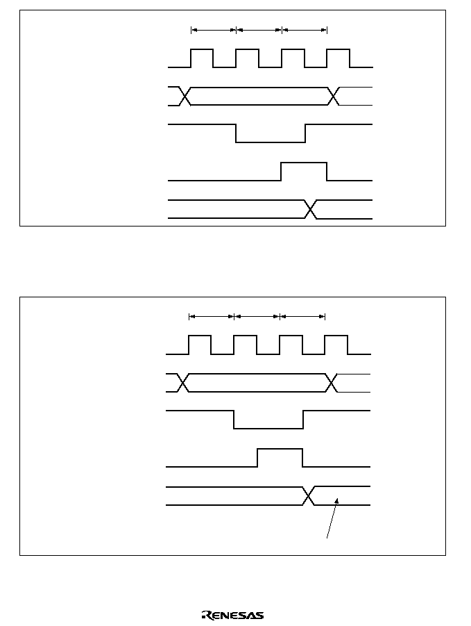
180
H'00
RTCNT
Address bus
Internal write signal
Counter clear signal
T
1
T
2
T
3
N
RTCNT address
Figure 6.39 Contention between RTCNT Write and Clear
Contention between RTCNT Write and Increment: If an increment pulse occurs in the T
3
state
of an RTCNT write cycle, writing takes priority and RTCNT is not incremented. See figure 6.40.
M
RTCNT
T
1
T
2
T
3
N
Address bus
RTCNT address
Internal write signal
RTCNT input clock
Counter write data
Figure 6.40 Contention between RTCNT Write and Increment
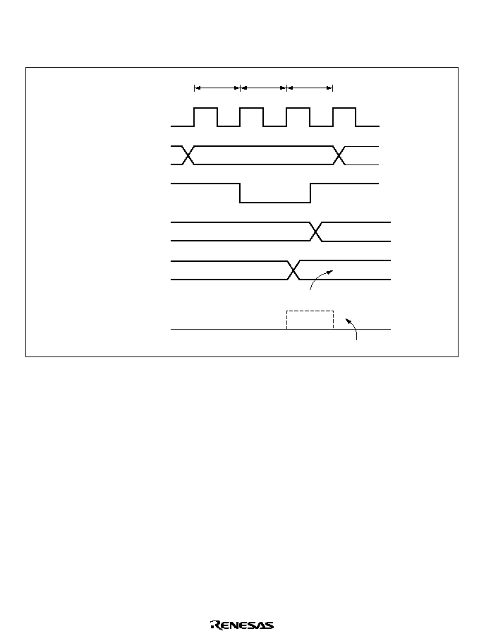
181
Contention between RTCOR Write and Compare Match: If a compare match occurs in the T
3
state of an RTCOR write cycle, writing takes priority and the compare match signal is inhibited.
See figure 6.41.
M
RTCOR
Compare match signal
T
1
T
2
T
3
N
N+1
N
RTCNT
Internal write signal
Address bus
RTCOR address
RTCOR write data
Inhibited
Figure 6.41 Contention between RTCOR Write and Compare Match
RTCNT Operation at Internal Clock Source Switchover: Switching internal clock sources may
cause RTCNT to increment, depending on the switchover timing. Table 6.10 shows the relation
between the time of the switchover (by writing to bits CKS2 to CKS0) and the operation of
RTCNT.
The RTCNT input clock is generated from the internal clock source by detecting the falling edge
of the internal clock. If a switchover is made from a high clock source to a low clock source, as in
case No. 3 in table 6.10, the switchover will be regarded as a falling edge, an RTCNT clock pulse
will be generated, and RTCNT will be incremented.
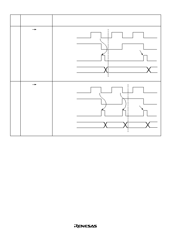
182
Table 6.10
Internal Clock Switchover and RTCNT Operation
N
N+1
No.
1
N
N+1
2
N+2
CKS2 to CKS0
Write Timing
RTCNT Operation
Low Low
switchover
*
1
Low High
switchover
*
2
Old clock source
New clock source
RTCNT clock
RTCNT
Old clock source
New clock source
RTCNT clock
RTCNT
CKS bits rewritten
CKS bits rewritten
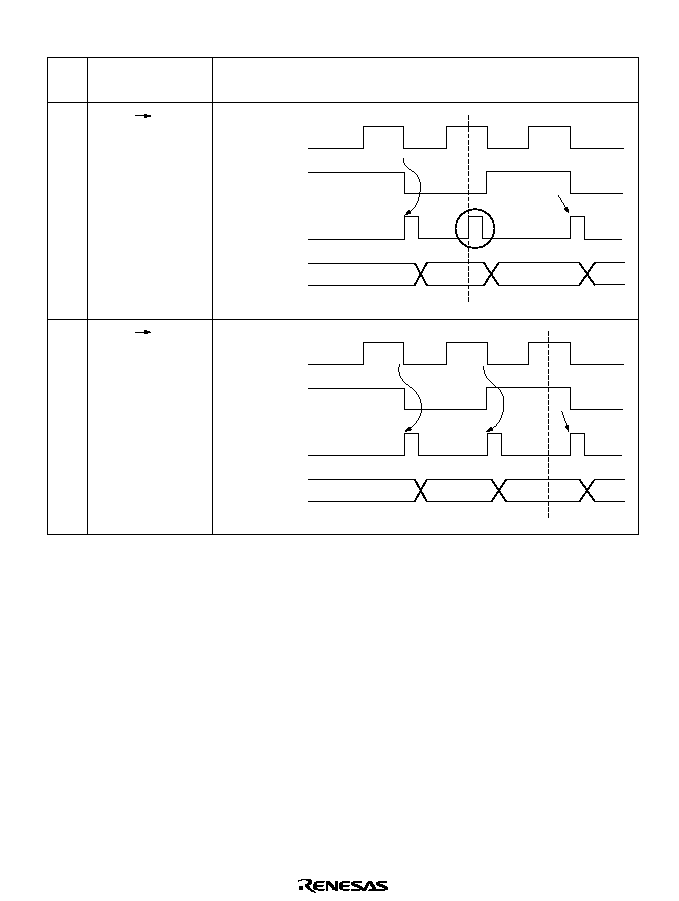
183
N
N+1
No.
3
N
N+1
RTCNT
4
N+2
N+2
*
4
*
1 Including switchovers from a low clock source to the halted state, and from the halted state to a low clock source.
*
2 Including switchover from the halted state to a high clock source.
*
3 Including switchover from a high clock source to the halted state.
*
4 The switchover is regarded as a falling edge, causing RTCNT to increment.
Notes:
CKS2 to CKS0
Write Timing
RTCNT Operation
High Low
switchover
*
3
High High
switchover
*
4
Old clock source
New clock source
RTCNT clock
RTCNT
Old clock source
New clock source
RTCNT clock
CKS bits rewritten
CKS bits rewritten

184
6.7
Interrupt Sources
Compare match interrupts (CMI) can be generated when the refresh timer is used as an interval
timer. Compare match interrupt requests are masked/unmasked with the CMIE bit in RTMCSR.
6.8
Burst ROM Interface
6.8.1
Overview
With the H8/3069F, external space area 0 can be designated as burst ROM space, and burst ROM
space interfacing can be performed. The burst ROM space interface enables 16-bit organization
ROM with burst access capability to be accessed at high speed. Area 0 is designated as burst
ROM space by means of the BROME bit in BCR.
Continuous burst access of a maximum or four or eight words can be performed on external space
area 0. Two or three states can be selected for burst access.
6.8.2
Basic Timing
The number of states in the initial cycle (full access) and a burst cycle of the burst ROM interface
is determined by the setting of the AST0 bit in ASTCR. When the AST0 bit is set to 1, wait states
can also be inserted in the initial cycle. Wait states cannot be inserted in a burst cycle.
Burst access of up to four words is performed when the BRSTS0 bit is cleared to 0 in BCR, and
burst access of up to eight words when the BRSTS0 bit is set to 1. The number of burst access
states is two when the BRSTS1 bit is cleared to 0, and three when the BRSTS1 bit is set to 1.
The basic access timing for burst ROM space is shown in figure 6.42.
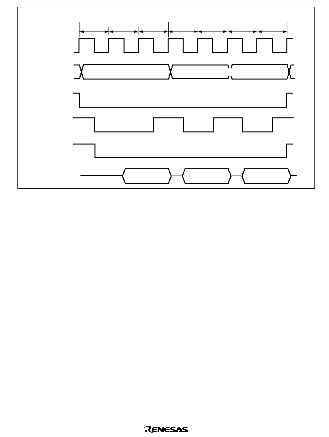
185
T
1
T
2
T
3
T
1
T
2
T
1
T
2
RD
AS
CS
0
Full access
Burst access
Address bus
Only lower address changes
Read data
Read data
Read data
Data bus
Figure 6.42 Example of Burst ROM Access Timing
6.8.3
Wait Control
As with the basic bus interface, either program wait insertion or pin wait insertion using the
WAIT
pin can be used in the initial cycle (full access) of the burst ROM interface.
Wait states cannot be inserted in a burst cycle.
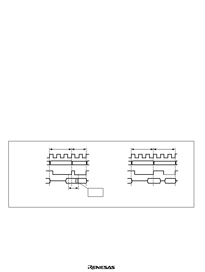
186
6.9
Idle Cycle
6.9.1
Operation
When the H8/3069F chip accesses external space, it can insert a 1-state idle cycle (T
I
) between bus
cycles in the following cases: (1) when read accesses between different areas occur consecutively,
(2) when a write cycle occurs immediately after a read cycle, and (3) immediately after a DRAM
space access. By inserting an idle cycle it is possible, for example, to avoid data collisions
between ROM, which has a long output floating time, and high-speed memory, I/O interfaces, and
so on.
The ICIS1 and ICIS0 bits in BCR both have an initial value of 1, so that an idle cycle is inserted in
the initial state. If there are no data collisions, the ICIS bits can be cleared.
Consecutive Reads between Different Areas: If consecutive reads between different areas occur
while the ICIS1 bit is set to 1 in BCR, an idle cycle is inserted at the start of the second read cycle.
Figure 6.43 shows an example of the operation in this case. In this example, bus cycle A is a read
cycle from ROM with a long output floating time, and bus cycle B is a read cycle from SRAM,
each being located in a different area. In (a), an idle cycle is not inserted, and a collision occurs in
cycle B between the read data from ROM and that from SRAM. In (b), an idle cycle is inserted,
and a data collision is prevented.
T
1
T
2
T
3
RD
T
1
T
2
T
1
T
2
T
3
T
i
T
2
T
1
Address bus
Data bus
RD
Address bus
Data bus
Bus cycle A Bus cycle B
Bus cycle A Bus cycle B
Data
collision
Long buffer-off
time
(a) Idle cycle not inserted
(b) Idle cycle inserted
Figure 6.43 Example of Idle Cycle Operation (1) (ICIS1 = 1)
Write after Read: If an external write occurs after an external read while the ICIS0 bit is set to 1
in BCR, an idle cycle is inserted at the start of the write cycle.
Figure 6.44 shows an example of the operation in this case. In this example, bus cycle A is a read
cycle from ROM with a long output floating time, and bus cycle B is a CPU write cycle.
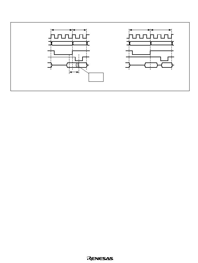
187
In (a), an idle cycle is not inserted, and a collision occurs in cycle B between the read data from
ROM and the CPU write data. In (b), an idle cycle is inserted, and a data collision is prevented.
T
1
T
2
T
3
RD
Address bus
Data bus
T
1
T
2
T
1
T
2
T
3
T
i
T
2
T
1
HWR
RD
Address bus
Data bus
HWR
Bus cycle A Bus cycle B
Bus cycle A Bus cycle B
Long buffer-off
time
Data
collision
(a) Idle cycle not inserted
(b) Idle cycle inserted
Figure 6.44 Example of Idle Cycle Operation (2) (ICIS0 = 1)
External Address Space Access Immediately after DRAM Space Access: If a DRAM space
access is followed by a non-DRAM external access when
HWR and LWR have been selected as
the
UCAS and LCAS output pins by means of the CSEL bit in DRCRB, a T
i
cycle is inserted
regardless of the settings of bits ICIS0 and ICIS1 in BCR. Figure 6.45 shows an example of the
operation.
This is done to prevent simultaneous changing of the
HWR and LWR signals used as UCAS and
LCAS in DRAM space and CSn for the space in the next cycle, and so avoid an erroneous write to
the external device in the next cycle.
A T
i
cycle is not inserted when PB
4
and PB
5
have been selected as the
UCAS and LCAS output
pins.
In the case of consecutive DRAM space access precharge cycles (T
p
), the ICIS0 bit settings are
invalid. In the case of consecutive reads between different areas, for example, if the second access
is a DRAM access, only a T
p
cycle is inserted, and a T
i
cycle is not. The timing in this case is
shown in figure 6.46.
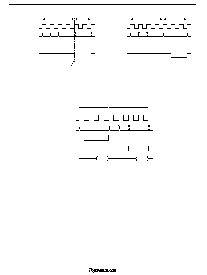
188
Address bus
Simultaneous change of
HWR
/
LWR
and
CSn
Tp
Tr
Tc1 Tc2
Bus cycle A
(DRAM access cycle)
HWR
/
LWR
(
UCAS
/
LCAS
)
T1
T2
Bus cycle B
CSn
Tp
Tr
Tc1 Tc2
T1
Ti
T2
Address bus
HWR
/
LWR
(
UCAS
/
LCAS
)
CSn
Bus cycle A
(DRAM access cycle) Bus cycle B
(a) Idle cycle not inserted
(b) Idle cycle inserted
Figure 6.45 Example of Idle Cycle Operation (3) (
HWR/LWR Used as UCAS/LCAS)
Address bus
T1
T2
T3
Address bus
UCAS
/
LCAS
RD
Tp
Tc1
Tr
Tc2
External read
DRAM space read
Figure 6.46 Example of Idle Cycle Operation (4) (Consecutive Precharge Cycles)
Usage Notes: When non-insertion of idle cycles is set, the rise (negation) of
RD and the fall
(assertion) of
CSn may occur simultaneously. An example of the operation is shown in figure
6.47.
If consecutive reads between different external areas occur while the ICIS1 bit is cleared to 0 in
BCR, or if a write cycle to a different external area occurs after an external read while the ICIS0
bit is cleared to 0, the
RD negation in the first read cycle and the CSn assertion in the following
bus cycle will occur simultaneously. Therefore, depending on the output delay time of each signal,
it is possible that the low-level output of
RD in the preceding read cycle and the low-level output
of
CSn in the following bus cycle will overlap.
A setting whereby idle cycle insertion is not performed can be made only when
RD and CSn do
not change simultaneously, or when it does not matter if they do.
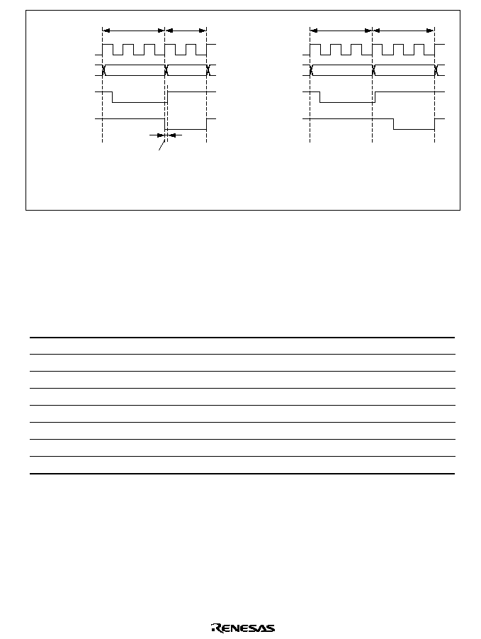
189
Address bus
T1
T2
T3
Bus cycle A
RD
T1
T2
(a) Idle cycle not inserted
T1
T2
T3
Ti
T2
(b) Idle cycle inserted
T1
Simultaneous change of
RD
and
CSn
Possibility of mutual overlap
CSn
Address bus
RD
CSn
Bus cycle B
Bus cycle A
Bus cycle B
Figure 6.47 Example of Idle Cycle Operation (5)
6.9.2
Pin States in Idle Cycle
Table 6.11 shows the pin states in an idle cycle.
Table 6.11
Pin States in Idle Cycle
Pins
Pin State
A
23
to A
0
Next cycle address value
D
15
to D
0
High impedance
CS
n
High
*
UCAS
,
LCAS
High
AS
High
RD
High
HWR
High
LWR
High
Note:
*
Remains low in DRAM space RAS down mode.

190
6.10
Bus Arbiter
The bus controller has a built-in bus arbiter that arbitrates between different bus masters. There
are four bus masters: the CPU, DMA controller (DMAC), DRAM interface, and an external bus
master. When a bus master has the bus right it can carry out read, write, or refresh access. Each
bus master uses a bus request signal to request the bus right. At fixed times the bus arbiter
determines priority and uses a bus acknowledge signal to grant the bus to a bus master, which can
the operate using the bus.
The bus arbiter checks whether the bus request signal from a bus master is active or inactive, and
returns an acknowledge signal to the bus master. When two or more bus masters request the bus,
the highest-priority bus master receives an acknowledge signal. The bus master that receives an
acknowledge signal can continue to use the bus until the acknowledge signal is deactivated.
The bus master priority order is:
(High)
External bus master > DRAM interface > DMAC > CPU
(Low)
The bus arbiter samples the bus request signals and determines priority at all times, but it does not
always grant the bus immediately, even when it receives a bus request from a bus master with
higher priority than the current bus master. Each bus master has certain times at which it can
release the bus to a higher-priority bus master.
6.10.1
Operation
CPU: The CPU is the lowest-priority bus master. If the DMAC, DRAM interface, or an external
bus master requests the bus while the CPU has the bus right, the bus arbiter transfers the bus right
to the bus master that requested it. The bus right is transferred at the following times:
�
The bus right is transferred at the boundary of a bus cycle. If word data is accessed by two
consecutive byte accesses, however, the bus right is not transferred between the two byte
accesses.
�
If another bus master requests the bus while the CPU is performing internal operations, such as
executing a multiply or divide instruction, the bus right is transferred immediately. The CPU
continues its internal operations.
�
If another bus master requests the bus while the CPU is in sleep mode, the bus right is
transferred immediately.
DMAC: When the DMAC receives an activation request, it requests the bus right from the bus
arbiter. If the DMAC is bus master and the DRAM interface or an external bus master requests
the bus, the bus arbiter transfers the bus right from the DMAC to the bus master that requested the
bus. The bus right is transferred at the following times.

191
The bus right is transferred when the DMAC finishes transferring one byte or one word. A
DMAC transfer cycle consists of a read cycle and a write cycle. The bus right is not transferred
between the read cycle and the write cycle.
There is a priority order among the DMAC channels. For details see section 7.4.9, Multiple-
Channel Operation.
DRAM Interface: The DRAM interface requests the bus right from the bus arbiter when a refresh
cycle request is issued, and releases the bus at the end of the refresh cycle. For details see section
6.5, DRAM Interface.
External Bus Master: When the BRLE bit is set to 1 in BRCR, the bus can be released to an
external bus master. The external bus master has highest priority, and requests the bus right from
the bus arbiter driving the
BREQ signal low. Once the external bus master acquires the bus, it
keeps the bus until the
BREQ signal goes high. While the bus is released to an external bus
master, the H8/3069F chip holds the address bus, data bus, bus control signals (
AS, RD, HWR,
and
LWR), and chip select signals (CSn: n = 7 to 0) in the high-impedance state, and holds the
BACK pin in the low output state.
The bus arbiter samples the
BREQ pin at the rise of the system clock (
). If
BREQ is low, the bus
is released to the external bus master at the appropriate opportunity. The
BREQ signal should be
held low until the
BACK signal goes low.
When the
BREQ pin is high in two consecutive samples, the BACK pin is driven high to end the
bus-release cycle.
Figure 6.48 shows the timing when the bus right is requested by an external bus master during a
read cycle in a two-state access area. There is a minimum interval of three states from when the
BREQ signal goes low until the bus is released.
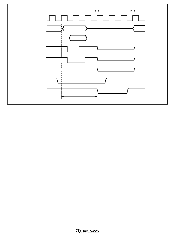
192
RD
BACK
(1)
(2)
(3)
(4)
(5)
(6)
BREQ
HWR
,
LWR
T
0
T
1
T
2
AS
Data bus
Address bus
CPU cycles
CPU cycles
External bus released
High
Address
Minimum 3 cycles
High-impedance
High-impedance
High-impedance
High-impedance
High-impedance
Figure 6.48 Example of External Bus Master Operation
In the event of contention with a bus request from an external bus master when a transition is
made to software standby mode, the
BACK and strobe states may be indeterminate after the
transition to software standby mode (see figure 6.36).
When software standby mode is used, the BRLE bit should be cleared to 0 in BRCR before
executing the SLEEP instruction.
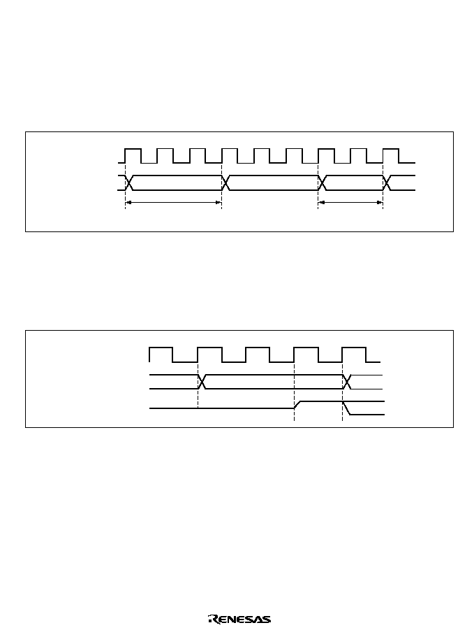
193
6.11
Register and Pin Input Timing
6.11.1
Register Write Timing
ABWCR, ASTCR, WCRH, and WCRL Write Timing: Data written to ABWCR, ASTCR,
WCRH, and WCRL takes effect starting from the next bus cycle. Figure 6.49 shows the timing
when an instruction fetched from area 0 changes area 0 from three-state access to two-state access.
T
1
T
2
T
3
T
1
T
2
T
3
T
1
T
2
Address bus
3-state access to area 0
2-state access to area 0
ASTCR address
Figure 6.49 ASTCR Write Timing
DDR and CSCR Write Timing: Data written to DDR or CSCR for the port corresponding to the
CSn pin to switch between CSn output and generic input takes effect starting from the T
3
state of
the DDR write cycle. Figure 6.50 shows the timing when the
CS
1
pin is changed from generic
input to
CS
1
output.
T
1
T
2
T
3
CS
1
Address bus
High-impedance
P8DDR address
Figure 6.50 DDR Write Timing
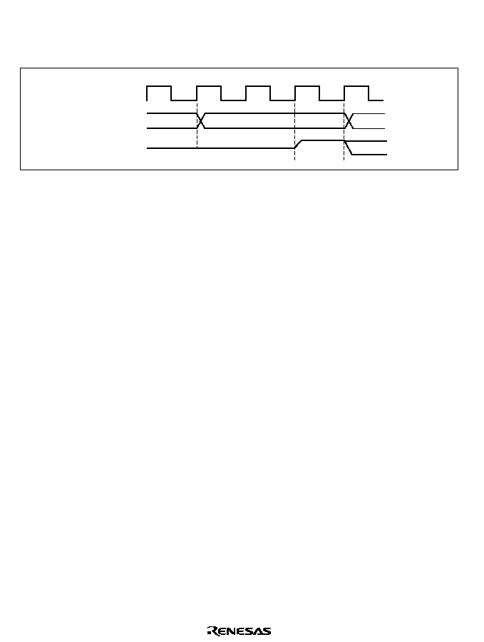
194
BRCR Write Timing: Data written to BRCR to switch between A
23
, A
22
, A
21
, or A
20
output and
generic input or output takes effect starting from the T
3
state of the BRCR write cycle. Figure
6.51 shows the timing when a pin is changed from generic input to A
23
, A
22
, A
21
, or A
20
output.
T
1
T
2
T
3
PA
7
to PA
4
(A
23
to A
20
)
Address bus
BRCR address
High-impedance
Figure 6.51 BRCR Write Timing
6.11.2
BREQ Pin Input Timing
After driving the
BREQ pin low, hold it low until BACK goes low. If BREQ returns to the high
level before
BACK goes lows, the bus arbiter may operate incorrectly.
To terminate the external-bus-released state, hold the
BREQ signal high for at least three states. If
BREQ is high for too short an interval, the bus arbiter may operate incorrectly.

195
Section 7 DMA Controller
7.1
Overview
The H8/3069F has an on-chip DMA controller (DMAC) that can transfer data on up to four
channels.
When the DMA controller is not used, it can be independently halted to conserve power. For
details see section 20.6, Module Standby Function.
7.1.1
Features
DMAC features are listed below.
�
Selection of short address mode or full address mode
Short address mode
8-bit source address and 24-bit destination address, or vice versa
Maximum four channels available
Selection of I/O mode, idle mode, or repeat mode
Full address mode
24-bit source and destination addresses
Maximum two channels available
Selection of normal mode or block transfer mode
�
Directly addressable 16-Mbyte address space
�
Selection of byte or word transfer
�
Activation by internal interrupts, external requests, or auto-request (depending on transfer
mode)
16-bit timer compare match/input capture interrupts (
�
3)
Serial communication interface (SCI channel 0) transmit-data-empty/receive-data-full
interrupts
External requests
Auto-request
A/D converter conversion-end interrupt
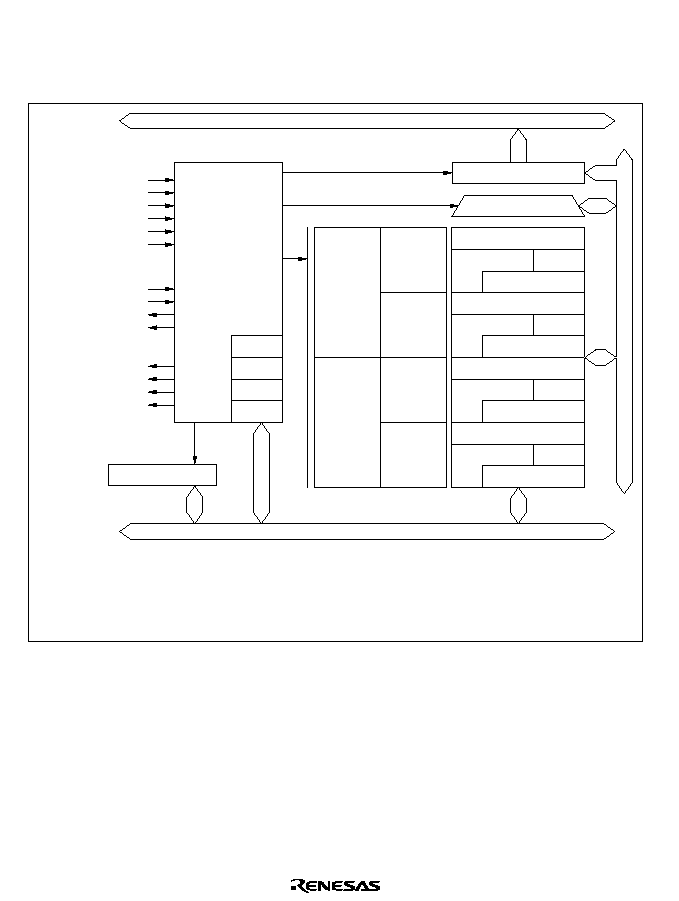
196
7.1.2
Block Diagram
Figure 7.1 shows a DMAC block diagram.
IMIA0
IMIA1
IMIA2
ADI
TXI0
RXI0
DREQ
0
DREQ
1
TEND
0
TEND
1
DEND0A
DEND0B
DEND1A
DEND1B
DTCR0A
DTCR0B
DTCR1A
DTCR1B
Control logic
Data buffer
Address buffer
Arithmetic-logic unit
MAR0A
MAR0B
MAR1A
MAR1B
IOAR0A
IOAR0B
IOAR1A
IOAR1B
ETCR0A
ETCR0B
ETCR1A
ETCR1B
Internal address bus
Internal
interrupts
Interrupt
signals
Internal data bus
Module data b
u
s
Legend
DTCR:
MAR:
IOAR:
ETCR:
Data transfer control register
Memory address register
I/O address register
Execute transfer count register
Channel
0A
Channel
0B
Channel
1A
Channel
1B
Channel
0
Channel
1
Figure 7.1 Block Diagram of DMAC

197
7.1.3
Functional Overview
Table 7.1 gives an overview of the DMAC functions.
Table 7.1
DMAC Functional Overview
Address
Reg. Length
Transfer Mode
Activation
Source
Destina-
tion
Short
address
mode
I/O mode
�
Transfers one byte or one word
per request
�
Increments or decrements the memory
address by 1 or 2
�
Executes 1 to 65,536 transfers
�
Compare match/input
capture A interrupts from 16-
bit timer channels
0 to 2
�
Transmit-data-empty
interrupt from SCI channel 0
24
8
Idle mode
�
Transfers one byte or one word per
request
�
Holds the memory address fixed
�
Conversion-end interrupt
from A/D converter
�
Receive-data-full interrupt
from SCI channel 0
8
24
�
Executes 1 to 65,536 transfers
Repeat mode
�
Transfers one byte or one word per
request
�
Increments or decrements the memory
address by 1 or 2
�
Executes a specified number (1 to
255) of transfers, then returns to the
initial state and continues
�
External request
24
8
Full
address
mode
Normal mode
�
Auto-request
Retains the transfer request
internally
Executes a specified number(1 to
65,536) of transfers continuously
Selection of burst mode or cycle-
steal mode
�
External request
Transfers one byte or one word
per request
Executes 1 to 65,536 transfers
�
Auto-request
�
External request
24
24
Block transfer
�
Transfers one block of a specified size
per request
�
Executes 1 to 65,536 transfers
�
Allows either the source or destination
to be a fixed block area
�
Block size can be 1 to 255 bytes or
words
�
Compare match/ input
capture A interrupts from 16-
bit timer channels 0 to 2
�
External request
�
Conversion-end interrupt
from A/D converter
24
24

198
7.1.4
Input/Output Pins
Table 7.2 lists the DMAC pins.
Table 7.2
DMAC Pins
Channel
Name
Abbrevia-
tion
Input/
Output
Function
0
DMA request 0
DREQ
0
Input
External request for DMAC channel 0
Transfer end 0
TEND
0
Output
Transfer end on DMAC channel 0
1
DMA request 1
DREQ
1
Input
External request for DMAC channel 1
Transfer end 1
TEND
1
Output
Transfer end on DMAC channel 1
Note: External requests cannot be made to channel A in short address mode.
7.1.5
Register Configuration
Table 7.3 lists the DMAC registers.

199
Table 7.3
DMAC Registers
Channel
Address
*
Name
Abbreviation R/W
Initial Value
0
H'FFF20
Memory address register 0AR
MAR0AR
R/W
Undetermined
H'FFF21
Memory address register 0AE
MAR0AE
R/W
Undetermined
H'FFF22
Memory address register 0AH
MAR0AH
R/W
Undetermined
H'FFF23
Memory address register 0AL
MAR0AL
R/W
Undetermined
H'FFF26
I/O address register 0A
IOAR0A
R/W
Undetermined
H'FFF24
Execute transfer count register 0AH ETCR0AH
R/W
Undetermined
H'FFF25
Execute transfer count register 0AL ETCR0AL
R/W
Undetermined
H'FFF27
Data transfer control register 0A
DTCR0A
R/W
H'00
H'FFF28
Memory address register 0BR
MAR0BR
R/W
Undetermined
H'FFF29
Memory address register 0BE
MAR0BE
R/W
Undetermined
H'FFF2A
Memory address register 0BH
MAR0BH
R/W
Undetermined
H'FFF2B
Memory address register 0BL
MAR0BL
R/W
Undetermined
H'FFF2E
I/O address register 0B
IOAR0B
R/W
Undetermined
H'FFF2C
Execute transfer count register 0BH ETCR0BH
R/W
Undetermined
H'FFF2D
Execute transfer count register 0BL ETCR0BL
R/W
Undetermined
H'FFF2F
Data transfer control register 0B
DTCR0B
R/W
H'00
1
H'FFF30
Memory address register 1AR
MAR1AR
R/W
Undetermined
H'FFF31
Memory address register 1AE
MAR1AE
R/W
Undetermined
H'FFF32
Memory address register 1AH
MAR1AH
R/W
Undetermined
H'FFF33
Memory address register 1AL
MAR1AL
R/W
Undetermined
H'FFF36
I/O address register 1A
IOAR1A
R/W
Undetermined
H'FFF34
Execute transfer count register 1AH ETCR1AH
R/W
Undetermined
H'FFF35
Execute transfer count register 1AL ETCR1AL
R/W
Undetermined
H'FFF37
Data transfer control register 1A
DTCR1A
R/W
H'00
H'FFF38
Memory address register 1BR
MAR1BR
R/W
Undetermined
H'FFF39
Memory address register 1BE
MAR1BE
R/W
Undetermined
H'FFF3A
Memory address register 1BH
MAR1BH
R/W
Undetermined
H'FFF3B
Memory address register 1BL
MAR1BL
R/W
Undetermined
H'FFF3E
I/O address register 1B
IOAR1B
R/W
Undetermined
H'FFF3C
Execute transfer count register 1BH ETCR1BH
R/W
Undetermined
H'FFF3D
Execute transfer count register 1BL ETCR1BL
R/W
Undetermined
H'FFF3F
Data transfer control register 1B
DTCR1B
R/W
H'00
Note:
*
The lower 20 bits of the address are indicated.
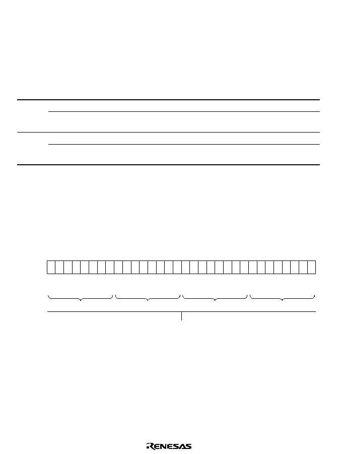
200
7.2
Register Descriptions (1) (Short Address Mode)
In short address mode, transfers can be carried out independently on channels A and B. Short
address mode is selected by bits DTS2A and DTS1A in data transfer control register A (DTCRA)
as indicated in table 7.4.
Table 7.4
Selection of Short and Full Address Modes
Channel
Bit 2
DTS2A
Bit 1
DTS1A
Description
0
1
1
DMAC channel 0 operates as one channel in full address mode
Other than above
DMAC channels 0A and 0B operate as two independent channels
in short address mode
1
1
1
DMAC channel 1 operates as one channel in full address mode
Other than above
DMAC channels 1A and 1B operate as two independent channels
in short address mode
7.2.1
Memory Address Registers (MAR)
A memory address register (MAR) is a 32-bit readable/writable register that specifies a source or
destination address. The transfer direction is determined automatically from the activation source.
An MAR consists of four 8-bit registers designated MARR, MARE, MARH, and MARL. All bits
of MARR are reserved; they cannot be modified and are always read as 1.
Bit
Initial value
Read/Write
31
--
Source or destination address
30
--
29
--
28
--
27
--
26
--
25
--
24
--
23
R/W
22
R/W
21
R/W
20
R/W
19
R/W
18
R/W
17
R/W
16
R/W
15
R/W
14
R/W
13
R/W
12
R/W
11
R/W
10
R/W
9
R/W
8
R/W
7
R/W
6
R/W
5
R/W
4
R/W
3
R/W
2
R/W
1
R/W
0
R/W
MARR
MARE
MARH
MARL
Undetermined
An MAR functions as a source or destination address register depending on how the DMAC is
activated: as a destination address register if activation is by a receive-data-full interrupt from
serial communication interface (SCI) channel 0 or by an A/D converter conversion-end interrupt,
and as a source address register otherwise.
The MAR value is incremented or decremented each time one byte or word is transferred,
automatically updating the source or destination memory address. For details, see section 7.3.4,
Data Transfer Control Registers (DTCR).
The MARs are not initialized by a reset or in standby mode.
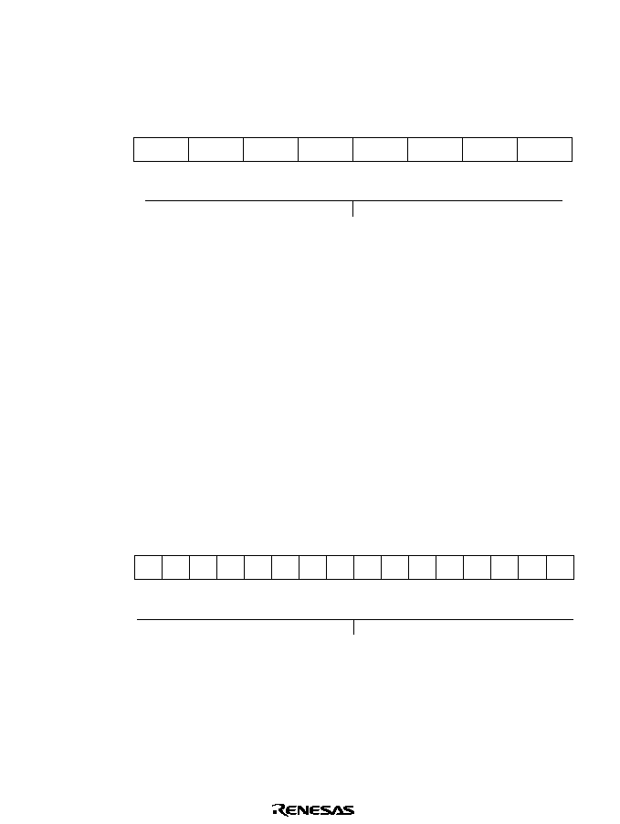
201
7.2.2
I/O Address Registers (IOAR)
An I/O address register (IOAR) is an 8-bit readable/writable register that specifies a source or
destination address. The IOAR value is the lower 8 bits of the address. The upper 16 address bits
are all 1 (H'FFFF).
Bit
Initial value
Read/Write
7
R/W
6
R/W
5
R/W
4
R/W
3
R/W
0
R/W
2
R/W
1
R/W
Source or destination address
Undetermined
An IOAR functions as a source or destination address register depending on how the DMAC is
activated: as a destination address register if activation is by a receive-data-full interrupt from
serial communication interface (SCI) channel 0 or by an A/D converter conversion-end interrupt,
and as a source address register otherwise.
The IOAR value is held fixed. It is not incremented or decremented when a transfer is executed.
The IOARs are not initialized by a reset or in standby mode.
7.2.3
Execute Transfer Count Registers (ETCR)
An execute transfer count register (ETCR) is a 16-bit readable/writable register that specifies the
number of transfers to be executed. These registers function in one way in I/O mode and idle
mode, and another way in repeat mode.
�
I/O mode and idle mode
Bit
Initial value
Read/Write
14
R/W
12
R/W
10
R/W
8
R/W
6
R/W
0
R/W
4
R/W
2
R/W
Transfer counter
Undetermined
15
R/W
13
R/W
11
R/W
9
R/W
7
R/W
1
R/W
5
R/W
3
R/W
In I/O mode and idle mode, ETCR functions as a 16-bit counter. The count is decremented by
1 each time one transfer is executed. The transfer ends when the count reaches H'0000.
202
�
Repeat mode
Bit
Initial value
Read/Write
7
R/W
6
R/W
5
R/W
4
R/W
3
R/W
0
R/W
2
R/W
1
R/W
Undetermined
Transfer counter
ETCRH
Bit
Initial value
Read/Write
7
R/W
6
R/W
5
R/W
4
R/W
3
R/W
0
R/W
2
R/W
1
R/W
Undetermined
Initial count
ETCRL
In repeat mode, ETCRH functions as an 8-bit transfer counter and ETCRL holds the initial transfer
count. ETCRH is decremented by 1 each time one transfer is executed. When ETCRH reaches
H'00, the value in ETCRL is reloaded into ETCRH and the same operation is repeated.
The ETCRs are not initialized by a reset or in standby mode.
203
7.2.4
Data Transfer Control Registers (DTCR)
A data transfer control register (DTCR) is an 8-bit readable/writable register that controls the
operation of one DMAC channel.
Bit
Initial value
Read/Write
7
DTE
0
R/W
6
DTSZ
0
R/W
5
DTID
0
R/W
4
RPE
0
R/W
3
DTIE
0
R/W
0
DTS0
0
R/W
2
DTS2
0
R/W
1
DTS1
0
R/W
Data transfer enable
Enables or disables
data transfer
Data transfer interrupt enable
Enables or disables the CPU interrupt
at the end of the transfer
Data transfer select
These bits select the data
transfer activation source
Data transfer size
Selects byte or
word size
Data transfer
increment/decrement
Selects whether to
increment or decrement
the memory address
register
Repeat enable
Selects repeat
mode
The DTCRs are initialized to H'00 by a reset and in standby mode.
Bit 7--Data Transfer Enable (DTE): Enables or disables data transfer on a channel. When the
DTE bit is set to 1, the channel waits for a transfer to be requested, and executes the transfer when
activated as specified by bits DTS2 to DTS0. When DTE is 0, the channel is disabled and does not
accept transfer requests. DTE is set to 1 by reading the register when DTE is 0, then writing 1.
Bit 7
DTE
Description
0
Data transfer is disabled. In I/O mode or idle mode, DTE is cleared to 0
(Initial value)
when the specified number of transfers have been completed
1
Data transfer is enabled
If DTIE is set to 1, a CPU interrupt is requested when DTIE is cleared to 0.

204
Bit 6--Data Transfer Size (DTSZ): Selects the data size of each transfer.
Bit 6
DTSZ
Description
0
Byte-size transfer
(Initial value)
1
Word-size transfer
Bit 5--Data Transfer Increment/Decrement (DTID): Selects whether to increment or
decrement the memory address register (MAR) after a data transfer in I/O mode or repeat mode.
Bit 5
DTID
Description
0
MAR is incremented after each data transfer
(Initial value)
�
If DTSZ = 0, MAR is incremented by 1 after each transfer
�
If DTSZ = 1, MAR is incremented by 2 after each transfer
1
MAR is decremented after each data transfer
�
If DTSZ = 0, MAR is decremented by 1 after each transfer
�
If DTSZ = 1, MAR is decremented by 2 after each transfer
MAR is not incremented or decremented in idle mode.
Bit 4--Repeat Enable (RPE): Selects whether to transfer data in I/O mode, idle mode, or repeat
mode.
Bit 4
RPE
Bit 3
DTIE
Description
0
0
I/O mode
(Initial value)
1
1
0
Repeat mode
1
Idle mode
Operations in these modes are described in sections 7.4.2, I/O Mode, 7.4.3, Idle Mode, and 7.4.4,
Repeat Mode.

205
Bit 3--Data Transfer Interrupt Enable (DTIE): Enables or disables the CPU interrupt (DEND)
requested when the DTE bit is cleared to 0.
Bit 3
DTIE
Description
0
The DEND interrupt requested by DTE is disabled
(Initial value)
1
The DEND interrupt requested by DTE is enabled
Bits 2 to 0--Data Transfer Select (DTS2, DTS1, DTS0): These bits select the data transfer
activation source. Some of the selectable sources differ between channels A and B.
Bit 2
DTS2
Bit 1
DTS1
Bit 0
DTS0
Description
0
0
0
Compare match/input capture A interrupt from 16-bit timer channel 0
(Initial value)
1
Compare match/input capture A interrupt from 16-bit timer channel 1
1
0
Compare match/input capture A interrupt from 16-bit timer channel 2
1
Conversion-end interrupt from A/D converter
1
0
0
Transmit-data-empty interrupt from SCI channel 0
1
Receive-data-full interrupt from SCI channel 0
1
0
Falling edge of
DREQ
input (channel B)
Transfer in full address mode (channel A)
1
Low level of
DREQ
input (channel B)
Transfer in full address mode (channel A)
Note:
See section 7.3.4, Data Transfer Control Registers (DTCR).
The same internal interrupt can be selected as an activation source for two or more channels at
once. In that case the channels are activated in a priority order, highest-priority channel first. For
the priority order, see section 7.4.9, Multiple-Channel Operation.
When a channel is enabled (DTE = 1), its selected DMAC activation source cannot generate a
CPU interrupt.
206
7.3
Register Descriptions (2) (Full Address Mode)
In full address mode the A and B channels operate together. Full address mode is selected as
indicated in table 7.4.
7.3.1
Memory Address Registers (MAR)
A memory address register (MAR) is a 32-bit readable/writable register. MARA functions as the
source address register of the transfer, and MARB as the destination address register.
An MAR consists of four 8-bit registers designated MARR, MARE, MARH, and MARL. All bits
of MARR are reserved; they cannot be modified and are always read as 1. (Write is invalid.)
Bit
Initial value
Read/Write
31
--
Source or destination address
30
--
29
--
28
--
27
--
26
--
25
--
24
--
23
R/W
22
R/W
21
R/W
20
R/W
19
R/W
18
R/W
17
R/W
16
R/W
15
R/W
14
R/W
13
R/W
12
R/W
11
R/W
10
R/W
9
R/W
8
R/W
7
R/W
6
R/W
5
R/W
4
R/W
3
R/W
2
R/W
1
R/W
0
R/W
MARR
MARE
MARH
MARL
Undetermined
The MAR value is incremented or decremented each time one byte or word is transferred,
automatically updating the source or destination memory address. For details, see section 7.3.4,
Data Transfer Control Registers (DTCR).
The MARs are not initialized by a reset or in standby mode.
7.3.2
I/O Address Registers (IOAR)
The I/O address registers (IOARs) are not used in full address mode.

207
7.3.3
Execute Transfer Count Registers (ETCR)
An execute transfer count register (ETCR) is a 16-bit readable/writable register that specifies the
number of transfers to be executed. The functions of these registers differ between normal mode
and block transfer mode.
�
Normal mode
ETCRA
Bit
Initial value
Read/Write
14
R/W
12
R/W
10
R/W
8
R/W
6
R/W
0
R/W
4
R/W
2
R/W
Transfer counter
Undetermined
15
R/W
13
R/W
11
R/W
9
R/W
7
R/W
1
R/W
5
R/W
3
R/W
ETCRB: Is not used in normal mode.
In normal mode ETCRA functions as a 16-bit transfer counter. The count is decremented by 1
each time one transfer is executed. The transfer ends when the count reaches H'0000. ETCRB is
not used.
208
�
Block transfer mode
ETCRA
Bit
Initial value
Read/Write
7
R/W
6
R/W
5
R/W
4
R/W
3
R/W
0
R/W
2
R/W
1
R/W
Undetermined
Block size counter
ETCRAH
Bit
Initial value
Read/Write
7
R/W
6
R/W
5
R/W
4
R/W
3
R/W
0
R/W
2
R/W
1
R/W
Undetermined
Initial block size
ETCRAL
ETCRB
Bit
Initial value
Read/Write
14
R/W
12
R/W
10
R/W
8
R/W
6
R/W
0
R/W
4
R/W
2
R/W
Block transfer counter
Undetermined
15
R/W
13
R/W
11
R/W
9
R/W
7
R/W
1
R/W
5
R/W
3
R/W
In block transfer mode, ETCRAH functions as an 8-bit block size counter. ETCRAL holds the
initial block size. ETCRAH is decremented by 1 each time one byte or word is transferred. When
the count reaches H'00, ETCRAH is reloaded from ETCRAL. Blocks consisting of an arbitrary
number of bytes or words can be transferred repeatedly by setting the same initial block size value
in ETCRAH and ETCRAL.
In block transfer mode ETCRB functions as a 16-bit block transfer counter. ETCRB is
decremented by 1 each time one block is transferred. The transfer ends when the count reaches
H'0000.
The ETCRs are not initialized by a reset or in standby mode.
209
7.3.4
Data Transfer Control Registers (DTCR)
The data transfer control registers (DTCRs) are 8-bit readable/writable registers that control the
operation of the DMAC channels. A channel operates in full address mode when bits DTS2A and
DTS1A are both set to 1 in DTCRA. DTCRA and DTCRB have different functions in full address
mode.
DTCRA
Bit
Initial value
Read/Write
7
DTE
0
R/W
6
DTSZ
0
R/W
5
SAID
0
R/W
4
SAIDE
0
R/W
3
DTIE
0
R/W
0
DTS0A
0
R/W
2
DTS2A
0
R/W
1
DTS1A
0
R/W
Data transfer enable
Enables or disables
data transfer
Enables or disables the
CPU interrupt at the end
of the transfer
Data transfer size
Selects byte or
word size
Source address
increment/decrement
Data transfer select
2A and 1A
These bits must both be
set to 1
Data transfer
interrupt enable
Source address increment/
decrement enable
These bits select whether
the source address register
(MARA) is incremented,
decremented, or held fixed
during the data transfer
Selects block
transfer mode
Data transfer
select 0A
DTCRA is initialized to H'00 by a reset and in standby mode.

210
Bit 7--Data Transfer Enable (DTE): Together with the DTME bit in DTCRB, this bit enables
or disables data transfer on the channel. When the DTME and DTE bits are both set to 1, the
channel is enabled. If auto-request is specified, data transfer begins immediately. Otherwise, the
channel waits for transfers to be requested. When the specified number of transfers have been
completed, the DTE bit is automatically cleared to 0. When DTE is 0, the channel is disabled and
does not accept transfer requests. DTE is set to 1 by reading the register when DTE is 0, then
writing 1.
Bit 7
DTE
Description
0
Data transfer is disabled (DTE is cleared to 0 when the specified number (Initial value)
of transfers have been completed)
1
Data transfer is enabled
If DTIE is set to 1, a CPU interrupt is requested when DTE is cleared to 0.
Bit 6--Data Transfer Size (DTSZ): Selects the data size of each transfer.
Bit 6
DTSZ
Description
0
Byte-size transfer
(Initial value)
1
Word-size transfer
Bit 5--Source Address Increment/Decrement (SAID) and,
Bit 4--Source Address Increment/Decrement Enable (SAIDE): These bits select whether the
source address register (MARA) is incremented, decremented, or held fixed during the data
transfer.
Bit 5
SAID
Bit 4
SAIDE
Description
0
0
MARA is held fixed
(Initial value)
1
MARA is incremented after each data transfer
�
If DTSZ = 0, MARA is incremented by 1 after each transfer
�
If DTSZ = 1, MARA is incremented by 2 after each transfer
1
0
MARA is held fixed
1
MARA is decremented after each data transfer
�
If DTSZ = 0, MARA is decremented by 1 after each transfer
�
If DTSZ = 1, MARA is decremented by 2 after each transfer

211
Bit 3--Data Transfer Interrupt Enable (DTIE): Enables or disables the CPU interrupt (DEND)
requested when the DTE bit is cleared to 0.
Bit 3
DTIE
Description
0
The DEND interrupt requested by DTE is disabled
(Initial value)
1
The DEND interrupt requested by DTE is enabled
Bits 2 and 1--Data Transfer Select 2A and 1A (DTS2A, DTS1A): A channel operates in full
address mode when DTS2A and DTS1A are both set to 1.
Bit 0--Data Transfer Select 0A (DTS0A): Selects normal mode or block transfer mode.
Bit 0
DTS0A
Description
0
Normal mode
(Initial value)
1
Block transfer mode
Operations in these modes are described in sections 7.4.5, Normal Mode, and 7.4.6, Block
Transfer Mode.
212
DTCRB
Bit
Initial value
Read/Write
7
DTME
0
R/W
6
--
0
R/W
5
DAID
0
R/W
4
DAIDE
0
R/W
3
TMS
0
R/W
0
DTS0B
0
R/W
2
DTS2B
0
R/W
1
DTS1B
0
R/W
Data transfer master enable
Enables or disables data
transfer, together with
the DTE bit, and is cleared
to 0 by an interrupt
Reserved bit
Destination address
increment/decrement
Data transfer select
2B to 0B
These bits select the data
transfer activation source
Transfer mode select
Destination address
increment/decrement enable
These bits select whether
the destination address
register (MARB) is incremented,
decremented, or held fixed
during the data transfer
Selects whether the
block area is the source
or destination in block
transfer mode
DTCRB is initialized to H'00 by a reset and in standby mode.
Bit 7--Data Transfer Master Enable (DTME): Together with the DTE bit in DTCRA, this bit
enables or disables data transfer. When the DTME and DTE bits are both set to 1, the channel is
enabled. When an NMI interrupt occurs DTME is cleared to 0, suspending the transfer so that the
CPU can use the bus. The suspended transfer resumes when DTME is set to 1 again. For further
information on operation in block transfer mode, see section 7.6.6, NMI Interrupts and Block
Transfer Mode.
DTME is set to 1 by reading the register while DTME = 0, then writing 1.
Bit 7
DTME
Description
0
Data transfer is disabled (DTME is cleared to 0 when an NMI interrupt
(Initial value)
occurs)
1
Data transfer is enabled

213
Bit 6--Reserved: Although reserved, this bit can be written and read.
Bit 5--Destination Address Increment/Decrement (DAID) and,
Bit 4--Destination Address Increment/Decrement Enable (DAIDE): These bits select whether
the destination address register (MARB) is incremented, decremented, or held fixed during the
data transfer.
Bit 5
DAID
Bit 4
DAIDE
Description
0
0
MARB is held fixed
(Initial value)
1
MARB is incremented after each data transfer
�
If DTSZ = 0, MARB is incremented by 1 after each data transfer
�
If DTSZ = 1, MARB is incremented by 2 after each data transfer
1
0
MARB is held fixed
1
MARB is decremented after each data transfer
�
If DTSZ = 0, MARB is decremented by 1 after each data transfer
�
If DTSZ = 1, MARB is decremented by 2 after each data transfer
Bit 3--Transfer Mode Select (TMS): Selects whether the source or destination is the block area
in block transfer mode.
Bit 3
TMS
Description
0
Destination is the block area in block transfer mode
(Initial value)
1
Source is the block area in block transfer mode

214
Bits 2 to 0--Data Transfer Select 2B to 0B (DTS2B, DTS1B, DTS0B): These bits select the
data transfer activation source. The selectable activation sources differ between normal mode and
block transfer mode.
Normal mode
Bit 2
DTS2B
Bit 1
DTS1B
Bit 0
DTS0B
Description
0
0
0
Auto-request (burst mode)
(Initial value)
1
Cannot be used
1
0
Auto-request (cycle-steal mode)
1
Cannot be used
1
0
0
Cannot be used
1
Cannot be used
1
0
Falling edge of
DREQ
1
Low level input at
DREQ
Block transfer mode
Bit 2
DTS2B
Bit 1
DTS1B
Bit 0
DTS0B Description
0
0
0
Compare match/input capture A interrupt from 16-bit timer channel 0
(Initial value)
1
Compare match/input capture A interrupt from 16-bit timer channel 1
1
0
Compare match/input capture A interrupt from 16-bit timer channel 2
1
Conversion-end interrupt from A/D converter
1
0
0
Cannot be used
1
Cannot be used
1
0
Falling edge of
DREQ
1
Cannot be used
The same internal interrupt can be selected to activate two or more channels. The channels are
activated in a priority order, highest priority first. For the priority order, see section 7.4.9,
Multiple-Channel Operation.

215
7.4
Operation
7.4.1
Overview
Table 7.5 summarizes the DMAC modes.
Table 7.5
DMAC Modes
Transfer Mode
Activation
Notes
Short address
mode
I/O mode
Idle mode
Repeat mode
Compare match/input
capture A interrupt from
16-bit timer channels 0 to 2
�
Up to four channels
can operate
independently
Transmit-data-empty
and receive-data-full
interrupts from SCI
channel 0
�
Only the B channels
support external requests
Conversion-end interrupt
from A/D converter
External request
Full address
mode
Normal mode
Auto-request
�
A and B channels are
paired; up to two
channels are available
External request
Block transfer mode
Compare match/input
capture A interrupt from
16-bit timer channels 0 to 2
�
Burst mode transfer or
cycle-steal mode transfer
can be selected for auto-
requests
Conversion-end interrupt
from A/D converter
External request
A summary of operations in these modes follows.
I/O Mode: One byte or word is transferred per request. A designated number of these transfers are
executed. A CPU interrupt can be requested at completion of the designated number of transfers.
One 24-bit address and one 8-bit address are specified. The transfer direction is determined
automatically from the activation source.
Idle Mode: One byte or word is transferred per request. A designated number of these transfers
are executed. A CPU interrupt can be requested at completion of the designated number of

216
transfers. One 24-bit address and one 8-bit address are specified. The addresses are held fixed. The
transfer direction is determined automatically from the activation source.
Repeat Mode: One byte or word is transferred per request. A designated number of these transfers
are executed. When the designated number of transfers are completed, the initial address and
counter value are restored and operation continues. No CPU interrupt is requested. One 24-bit
address and one 8-bit address are specified. The transfer direction is determined automatically
from the activation source.
Normal Mode
�
Auto-request
The DMAC is activated by register setup alone, and continues executing transfers until the
designated number of transfers have been completed. A CPU interrupt can be requested at
completion of the transfers. Both addresses are 24-bit addresses.
Cycle-steal mode
The bus is released to another bus master after each byte or word is transferred.
Burst mode
Unless requested by a higher-priority bus master, the bus is not released until the
designated number of transfers have been completed.
�
External request
One byte or word is transferred per request. A designated number of these transfers are
executed. A CPU interrupt can be requested at completion of the designated number of
transfers. Both addresses are 24-bit addresses.
Block Transfer Mode: One block of a specified size is transferred per request. A designated
number of block transfers are executed. At the end of each block transfer, one address is restored
to its initial value. When the designated number of blocks have been transferred, a CPU interrupt
can be requested. Both addresses are 24-bit addresses.
217
7.4.2
I/O Mode
I/O mode can be selected independently for each channel.
One byte or word is transferred at each transfer request in I/O mode. A designated number of these
transfers are executed. One address is specified in the memory address register (MAR), the other
in the I/O address register (IOAR). The direction of transfer is determined automatically from the
activation source. The transfer is from the address specified in IOAR to the address specified in
MAR if activated by an SCI channel 0 receive-data-full interrupt, and from the address specified
in MAR to the address specified in IOAR otherwise.
Table 7.6 indicates the register functions in I/O mode.
Table 7.6
Register Functions in I/O Mode
Function
Register
Activated by
SCI 0 Receive-
Data-Full
Interrupt
Other
Activation
Initial Setting
Operation
23
0
MAR
Destination
address
register
Source
address
register
Destination or
source start
address
Incremented or
decremented
once per
transfer
All 1s
IOAR
23
0
7
Source
address
register
Destination
address
register
Source or
destination
address
Held fixed
15
0
ETCR
Transfer counter
Number of
transfers
Decremented
once per
transfer until
H'0000 is
reached and
transfer ends
Legend
MAR:
Memory address register
IOAR: I/O address register
ETCR: Execute transfer count register
MAR and IOAR specify the source and destination addresses. MAR specifies a 24-bit source or
destination address, which is incremented or decremented as each byte or word is transferred.
IOAR specifies the lower 8 bits of a fixed address. The upper 16 bits are all 1s. IOAR is not
incremented or decremented.
Figure 7.2 illustrates how I/O mode operates.
218
Address T
Address B
Transfer
Legend
L = initial setting of MAR
N = initial setting of ETCR
Address T = L
Address B = L + (�1) � (2 � N � 1)
DTID
IOAR
1 byte or word is
transferred per request
DTSZ
Figure 7.2 Operation in I/O Mode
The transfer count is specified as a 16-bit value in ETCR. The ETCR value is decremented by 1 at
each transfer. When the ETCR value reaches H'0000, the DTE bit is cleared and the transfer ends.
If the DTIE bit is set to 1, a CPU interrupt is requested at this time. The maximum transfer count is
65,536, obtained by setting ETCR to H'0000.
Transfers can be requested (activated) by compare match/input capture A interrupts from 16-bit
timer channels 0 to 2, transmit-data-empty and receive-data-full interrupts from SCI channel 0,
conversion-end interrupts from the A/D converter, and external request signals.
For the detailed settings see section 7.2.4, Data Transfer Control Registers (DTCR).
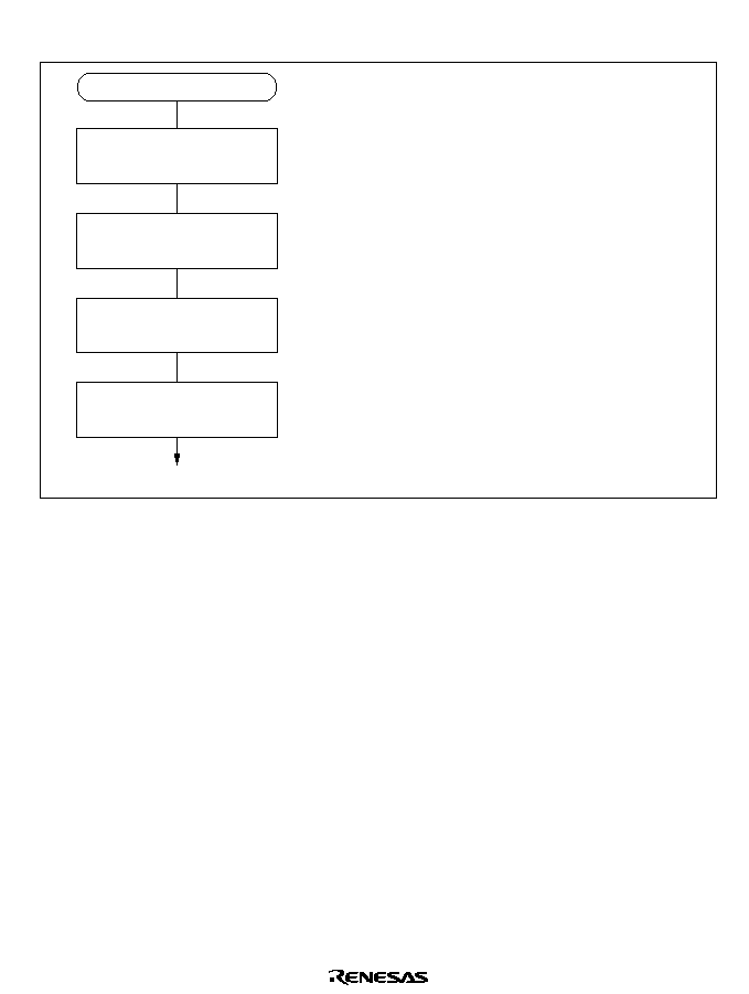
219
Figure 7.3 shows a sample setup procedure for I/O mode.
Set source and
destination addresses
Set transfer count
Read DTCR
Set DTCR
I/O mode
I/O mode setup
1
2
3
4
1.
2.
3.
4.
Set the source and destination addresses
in MAR and IOAR. The transfer direction is
determined automatically from the activation
source.
Set the transfer count in ETCR.
Read DTCR while the DTE bit is cleared to 0.
Set the DTCR bits as follows.
Select the DMAC activation source with bits
DTS2 to DTS0.
Set or clear the DTIE bit to enable or disable
the CPU interrupt at the end of the transfer.
Clear the RPE bit to 0 to select I/O mode.
Select MAR increment or decrement with the
DTID bit.
Select byte size or word size with the DTSZ bit.
Set the DTE bit to 1 to enable the transfer.
�
�
�
�
�
�
Figure 7.3 I/O Mode Setup Procedure (Example)
7.4.3
Idle Mode
Idle mode can be selected independently for each channel.
One byte or word is transferred at each transfer request in idle mode. A designated number of
these transfers are executed. One address is specified in the memory address register (MAR), the
other in the I/O address register (IOAR). The direction of transfer is determined automatically
from the activation source. The transfer is from the address specified in IOAR to the address
specified in MAR if activated by an SCI channel 0 receive-data-full interrupt, and from the
address specified in MAR to the address specified in IOAR otherwise.
Table 7.7 indicates the register functions in idle mode.
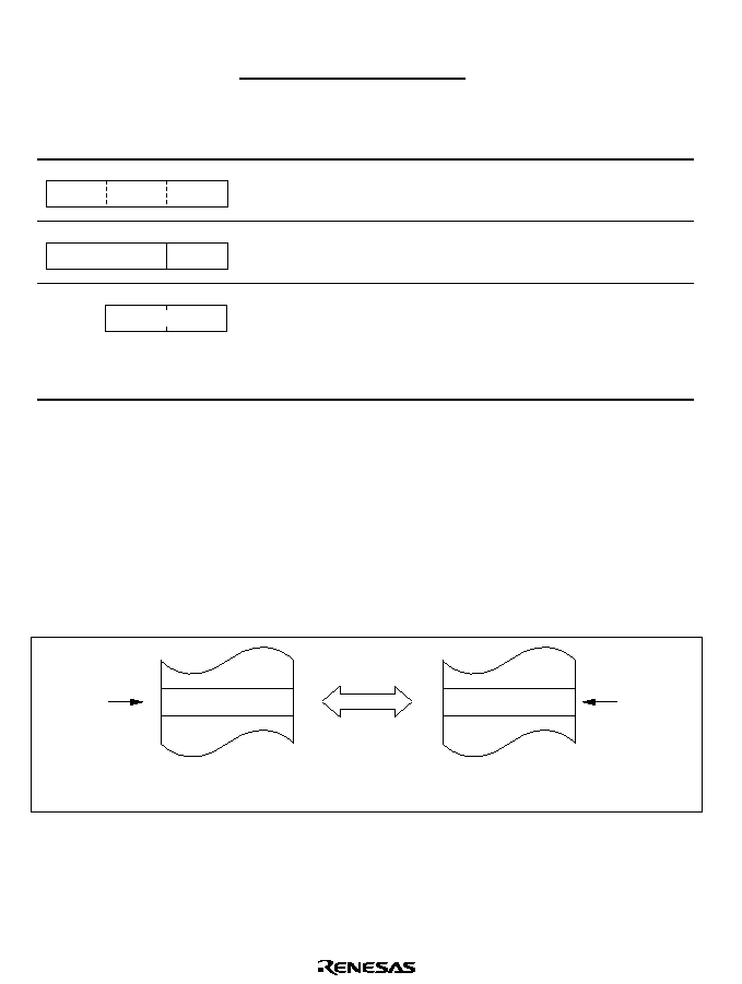
220
Table 7.7 Register Functions in Idle Mode
Function
Register
Activated by
SCI 0 Receive-
Data-Full
Interrupt
Other
Activation
Initial Setting
Operation
23
0
MAR
Destination
address
register
Source
address
register
Destination or
source address
Held fixed
All 1s
IOAR
23
0
7
Source
address
register
Destination
address
register
Source or
destination
address
Held fixed
15
0
ETCR
Transfer counter
Number of
transfers
Decremented
once per
transfer until
H'0000 is
reached and
transfer ends
Legend
MAR:
Memory address register
IOAR: I/O address register
ETCR: Execute transfer count register
MAR and IOAR specify the source and destination addresses. MAR specifies a 24-bit source or
destination address. IOAR specifies the lower 8 bits of a fixed address. The upper 16 bits are all
1s. MAR and IOAR are not incremented or decremented.
Figure 7.4 illustrates how idle mode operates.
Transfer
1 byte or word is
transferred per request
IOAR
MAR
Figure 7.4 Operation in Idle Mode
221
The transfer count is specified as a 16-bit value in ETCR. The ETCR value is decremented by 1 at
each transfer. When the ETCR value reaches H'0000, the DTE bit is cleared, the transfer ends, and
a CPU interrupt is requested. The maximum transfer count is 65,536, obtained by setting ETCR to
H'0000.
Transfers can be requested (activated) by compare match/input capture A interrupts from 16-bit
timer channels 0 to 2, transmit-data-empty and receive-data-full interrupts from SCI channel 0,
conversion-end interrupts from the A/D converter, and external request signals.
For the detailed settings see section 7.3.4, Data Transfer Control Registers (DTCR).
Figure 7.5 shows a sample setup procedure for idle mode.
Set source and
destination addresses
Set transfer count
Read DTCR
Set DTCR
Idle mode
Idle mode setup
1
2
3
4
1.
2.
3.
4.
Set the source and destination addresses
in MAR and IOAR. The transfer direction is deter-
mined automatically from the activation source.
Set the transfer count in ETCR.
Read DTCR while the DTE bit is cleared to 0.
Set the DTCR bits as follows.
Select the DMAC activation source with bits
DTS2 to DTS0.
Set the DTIE and RPE bits to 1 to select idle mode.
Select byte size or word size with the DTSZ bit.
Set the DTE bit to 1 to enable the transfer.
�
�
�
�
Figure 7.5 Idle Mode Setup Procedure (Example)
222
7.4.4
Repeat Mode
Repeat mode is useful for cyclically transferring a bit pattern from a table to the programmable
timing pattern controller (TPC) in synchronization, for example, with 16-bit timer compare match.
Repeat mode can be selected for each channel independently.
One byte or word is transferred per request in repeat mode, as in I/O mode. A designated number
of these transfers are executed. One address is specified in the memory address register (MAR),
the other in the I/O address register (IOAR). At the end of the designated number of transfers,
MAR and ETCRH are restored to their original values and operation continues. The direction of
transfer is determined automatically from the activation source. The transfer is from the address
specified in IOAR to the address specified in MAR if activated by an SCI channel 0 receive-data-
full interrupt, and from the address specified in MAR to the address specified in IOAR otherwise.
Table 7.8 indicates the register functions in repeat mode.
Table 7.8
Register Functions in Repeat Mode
Function
Register
Activated by
SCI 0 Receive-
Data-Full
Interrupt
Other
Activation Initial Setting
Operation
Destination
address
register
Source
address
register
Destination or
source start
address
Incremented or
decremented at
each transfer until
ETCRH reaches
H'0000, then restored
to initial value
Source
address
register
Destination
address
register
Source or
destination
address
Held fixed
Transfer counter
Number of
transfers
Decremented once
per transfer until
H'0000 is reached,
then reloaded from
ETCRL
Initial transfer count
Number of
transfers
Held fixed
Legend
MAR:
Memory address register
IOAR: I/O address register
ETCR: Execute transfer count register
23
0
MAR
All 1s
IOAR
23
0
7
0
ETCRH
7
7
0
ETCRL
223
In repeat mode ETCRH is used as the transfer counter while ETCRL holds the initial transfer
count. ETCRH is decremented by 1 at each transfer until it reaches H'00, then is reloaded from
ETCRL. MAR is also restored to its initial value, which is calculated from the DTSZ and DTID
bits in DTCR. Specifically, MAR is restored as follows:
MAR
MAR � (�1)
DTID
� 2
DTSZ
� ETCRL
ETCRH and ETCRL should be initially set to the same value.
In repeat mode transfers continue until the CPU clears the DTE bit to 0. After DTE is cleared to 0,
if the CPU sets DTE to 1 again, transfers resume from the state at which DTE was cleared. No
CPU interrupt is requested.
As in I/O mode, MAR and IOAR specify the source and destination addresses. MAR specifies a
24-bit source or destination address. IOAR specifies the lower 8 bits of a fixed address. The upper
16 bits are all 1s. IOAR is not incremented or decremented.
Figure 7.6 illustrates how repeat mode operates.
Address T
Address B
Transfer
1 byte or word is
transferred per request
Legend
L = initial setting of MAR
N = initial setting of ETCRH and ETCRL
Address T = L
Address B = L + (�1) � (2 � N � 1)
DTID
DTSZ
IOAR
Figure 7.6 Operation in Repeat Mode
224
The transfer count is specified as an 8-bit value in ETCRH and ETCRL. The maximum transfer
count is 255, obtained by setting both ETCRH and ETCRL to H'FF.
Transfers can be requested (activated) by compare match/input capture A interrupts from 16-bit
timer channels 0 to 2, transmit-data-empty and receive-data-full interrupts from SCI channel 0,
conversion-end interrupts from the A/D converter, and external request signals.
For the detailed settings see section 7.2.4, Data Transfer Control Registers (DTCR).
Figure 7.7 shows a sample setup procedure for repeat mode.
Set source and
destination addresses
Set transfer count
Read DTCR
Set DTCR
Repeat mode
Repeat mode
1
2
3
4
1.
2.
3.
4.
Set the source and destination addresses in MAR
and IOAR. The transfer direction is determined
automatically from the activation source.
Set the transfer count in both ETCRH and ETCRL.
Read DTCR while the DTE bit is cleared to 0.
Select byte size or word size with the DTSZ bit.
Set the DTE bit to 1 to enable the transfer.
�
�
�
�
�
Select the DMAC activation source with bits
DTS2 to DTS0.
Clear the DTIE bit to 0 and set the RPE bit to 1
to select repeat mode.
Select MAR increment or decrement with the DTID bit.
Set the DTCR bits as follows.
Figure 7.7 Repeat Mode Setup Procedure (Example)
225
7.4.5
Normal Mode
In normal mode the A and B channels are combined. One byte or word is transferred per request.
A designated number of these transfers are executed. Addresses are specified in MARA and
MARB. Table 7.9 indicates the register functions in I/O mode.
Table 7.9
Register Functions in Normal Mode
Register
Function
Initial Setting
Operation
23
0
MARA
Source address
register
Source start
address
Incremented or
decremented once per
transfer, or held fixed
23
0
MARB
Destination
address register
Destination start
address
Incremented or
decremented once per
transfer, or held fixed
15
0
ETCRA
Transfer counter
Number of
transfers
Decremented once per
transfer
Legend
MARA: Memory address register A
MARB: Memory address register B
ETCRA: Execute transfer count register A
The source and destination addresses are both 24-bit addresses. MARA specifies the source
address. MARB specifies the destination address. MARA and MARB can be independently
incremented, decremented, or held fixed as data is transferred.
The transfer count is specified as a 16-bit value in ETCRA. The ETCRA value is decremented by
1 at each transfer. When the ETCRA value reaches H'0000, the DTE bit is cleared and the transfer
ends. If the DTIE bit is set to 1, a CPU interrupt is requested at this time. The maximum transfer
count is 65,536, obtained by setting ETCRA to H'0000.
226
Figure 7.8 illustrates how normal mode operates.
Address T
Address B
Transfer
Legend
L
L
N
T
B
T
B
SAID
DAID
Address T
Address B
A
B
A
A
B
B
= initial setting of MARA
= initial setting of MARB
= initial setting of ETCRA
= L
= L + SAIDE � (�1) � (2 � N � 1)
= L
= L + DAIDE � (�1) � (2 � N � 1)
A
A
B
B
DTSZ
DTSZ
A
A
B
B
Figure 7.8 Operation in Normal Mode
Transfers can be requested (activated) by an external request or auto-request. An auto-requested
transfer is activated by the register settings alone. The designated number of transfers are executed
automatically. Either cycle-steal or burst mode can be selected. In cycle-steal mode the DMAC
releases the bus temporarily after each transfer. In burst mode the DMAC keeps the bus until the
transfers are completed, unless there is a bus request from a higher-priority bus master.
For the detailed settings see section 7.3.4, Data Transfer Control Registers (DTCR).
227
Figure 7.9 shows a sample setup procedure for normal mode.
1.
2.
3.
4.
5.
6.
7.
8.
9.
Set the initial source address in MARA.
Set the initial destination address in MARB.
Set the transfer count in ETCRA.
Set the DTCRB bits as follows.
Set the DTCRA bits as follows.
Read DTCRB with DTME cleared to 0.
Normal mode
Normal mode
Set initial source address
Set initial destination address
Set transfer count
Set DTCRB (1)
Set DTCRA (1)
Read DTCRB
Set DTCRB (2)
Read DTCRA
Set DTCRA (2)
1
2
3
4
5
6
7
8
9
�
�
�
�
�
�
�
�
Clear the DTME bit to 0.
Set the DAID and DAIDE bits to select whether
MARB is incremented, decremented, or held fixed.
Select the DMAC activation source with bits
DTS2B to DTS0B.
Clear the DTE bit to 0.
Select byte or word size with the DTSZ bit.
Set the SAID and SAIDE bits to select whether
MARA is incremented, decremented, or held fixed.
Set or clear the DTIE bit to enable or disable the
CPU interrupt at the end of the transfer.
Clear the DTS0A bit to 0 and set the DTS2A
and DTS1A bits to 1 to select normal mode.
Set the DTME bit to 1 in DTCRB.
Read DTCRA with DTE cleared to 0.
Set the DTE bit to 1 in DTCRA to enable the transfer.
Note: Carry out settings 1 to 9 with the DEND interrupt masked in the CPU.
If an NMI interrupt occurs during the setup procedure, it may clear the DTME bit to 0, in
which case the transfer will not start.
Figure 7.9 Normal Mode Setup Procedure (Example)
228
7.4.6
Block Transfer Mode
In block transfer mode the A and B channels are combined. One block of a specified size is
transferred per request. A designated number of block transfers are executed. Addresses are
specified in MARA and MARB. The block area address can be either held fixed or cycled.
Table 7.10 indicates the register functions in block transfer mode.
Table 7.10
Register Functions in Block Transfer Mode
Register
Function
Initial Setting
Operation
Source address
register
Source start
address
Incremented or
decremented once per
transfer, or held fixed
Destination
address register
Destination start
address
Incremented or
decremented once per
transfer, or held fixed
Block size counter
Block size
Decremented once per
transfer until H'00 is
reached, then reloaded
from ETCRL
Initial block size
Block size
Held fixed
Block transfer
counter
Number of block
transfers
Decremented once per
block transfer until H'0000
is reached and the
transfer ends
Legend
MARA: Memory address register A
MARB: Memory address register B
ETCRA: Execute transfer count register A
ETCRB: Execute transfer count register B
23
0
MARA
7
0
ETCRAH
7
0
ETCRAL
23
0
MARB
15
0
ETCRB
The source and destination addresses are both 24-bit addresses. MARA specifies the source
address. MARB specifies the destination address. MARA and MARB can be independently
incremented, decremented, or held fixed as data is transferred. One of these registers operates as a
block area register: even if it is incremented or decremented, it is restored to its initial value at the
end of each block transfer. The TMS bit in DTCRB selects whether the block area is the source or
destination.
229
If M (1 to 255) is the size of the block transferred at each request and N (1 to 65,536) is the
number of blocks to be transferred, then ETCRAH and ETCRAL should initially be set to M and
ETCRB should initially be set to N.
Figure 7.10 illustrates how block transfer mode operates. In this figure, bit TMS is cleared to 0,
meaning the block area is the destination.
T
B
Transfer
Legend
L
L
M
N
T
B
T
B
Address T
M bytes or words are
transferred per request
Address B
A
A
Block 1
Block N
B
B
Block area
Block 2
= initial setting of MARA
= initial setting of MARB
= initial setting of ETCRAH and ETCRAL
= initial setting of ETCRB
= L
= L + SAIDE � (�1) � (2 � M � 1)
= L
= L + DAIDE � (�1) � (2 � M � 1)
A
A
B
B
A
B
A
A
B
B
SAID
DAID
DTSZ
DTSZ
Figure 7.10 Operation in Block Transfer Mode

230
When activated by a transfer request, the DMAC executes a burst transfer. During the transfer
MARA and MARB are updated according to the DTCR settings, and ETCRAH is decremented.
When ETCRAH reaches H'00, it is reloaded from ETCRAL to restore the initial value. The
memory address register of the block area is also restored to its initial value, and ETCRB is
decremented. If ETCRB is not H'0000, the DMAC then waits for the next transfer request.
ETCRAH and ETCRAL should be initially set to the same value.
The above operation is repeated until ETCRB reaches H'0000, at which point the DTE bit is
cleared to 0 and the transfer ends. If the DTIE bit is set to 1, a CPU interrupt is requested at this
time.
Figure 7.11 shows examples of a block transfer with byte data size when the block area is the
destination. In (a) the block area address is cycled. In (b) the block area address is held fixed.
Transfers can be requested (activated) by compare match/input capture A interrupts from ITU
channels 0 to 2, by an A/D converter conversion-end interrupt, and by external request signals.
For the detailed settings see section 7.3.4, Data Transfer Control Registers (DTCR).
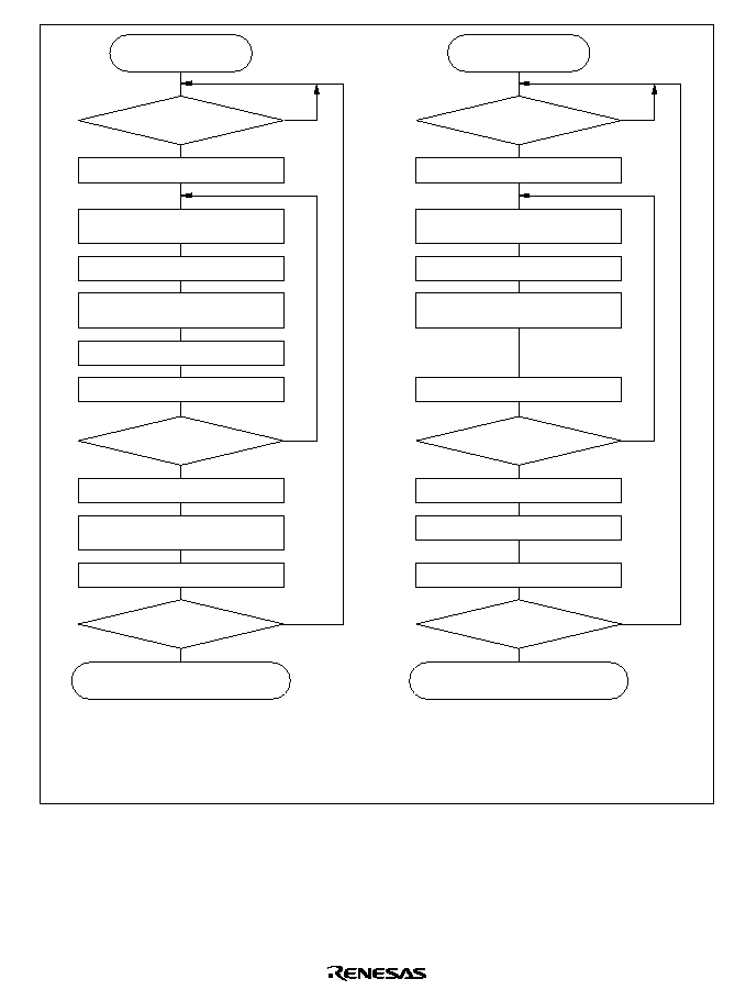
231
Start
(DTE = DTME = 1)
Transfer requested?
Get bus
MARA = MARA + 1
Read from MARA address
Write to MARB address
MARB = MARB + 1
ETCRAH = ETCRAH � 1
ETCRAH = H'00
Release bus
Clear DTE to 0 and end transfer
ETCRAH = ETCRAL
MARB = MARB � ETCRAL
ETCRB = ETCRB � 1
ETCRB = H'0000
Start
(DTE = DTME = 1)
Transfer requested?
Get bus
MARA = MARA + 1
Read from MARA address
Write to MARB address
ETCRAH = ETCRAH � 1
ETCRAH = H'00
Release bus
Clear DTE to 0 and end transfer
ETCRB = ETCRB � 1
ETCRB = H'0000
ETCRAH = ETCRAL
No
No
No
Yes
Yes
Yes
No
No
No
Yes
Yes
Yes
a. DTSZ = TMS = 0
SAID = DAID = 0
SAIDE = DAIDE = 1
b. DTSZ = TMS = 0
SAID = 0
SAIDE = 1
DAIDE = 0
Figure 7.11 Block Transfer Mode Flowcharts (Examples)
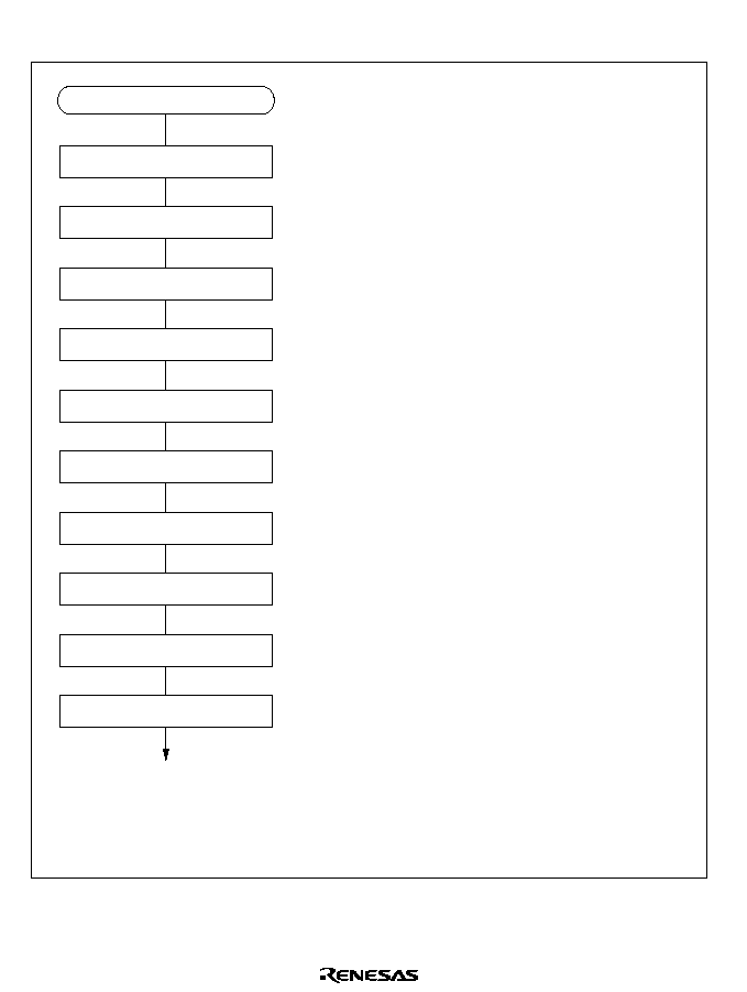
232
Figure 7.12 shows a sample setup procedure for block transfer mode.
1.
2.
3.
4.
5.
6.
7.
8.
9.
10.
Block transfer mode
1
2
3
4
5
6
7
8
9
10
Set source address
Set destination address
Set block transfer count
Set block size
Set DTCRB (1)
Set DTCRA (1)
Read DTCRB
Set DTCRB (2)
Read DTCRA
Set DTCRA (2)
Block transfer mode
Set the source address in MARA.
Set the destination address in MARB.
Set the block transfer count in ETCRB.
Set the block size (number of bytes or words)
in both ETCRAH and ETCRAL.
Set the DTCRB bits as follows.
Set the DTCRA bits as follows.
�
�
�
�
�
�
�
�
�
Clear the DTME bit to 0.
Set the DAID and DAIDE bits to select whether
MARB is incremented, decremented, or held fixed.
Set or clear the TMS bit to make the block area
the source or destination.
Select the DMAC activation source with bits
DTS2B to DTS0B.
Clear the DTE to 0.
Select byte size or word size with the DTSZ bit.
Set the SAID and SAIDE bits to select whether
MARA is incremented, decremented, or held fixed.
Set or clear the DTIE bit to enable or disable the
CPU interrupt at the end of the transfer.
Set bits DTS2A to DTS0A all to 1 to select
block transfer mode.
Read DTCRB with DTME cleared to 0.
Set the DTME bit to 1 in DTCRB.
Read DTCRA with DTE cleared to 0.
Set the DTE bit to 1 in DTCRA to enable
the transfer.
Note: Carry out settings 1 to 10 with the DEND interrupt masked in the CPU.
If an NMI interrupt occurs during the setup procedure, it may clear the DTME bit to 0, in
which case the transfer will not start.
Figure 7.12 Block Transfer Mode Setup Procedure (Example)
233
7.4.7
DMAC Activation
The DMAC can be activated by an internal interrupt, external request, or auto-request. The
available activation sources differ depending on the transfer mode and channel as indicated in
table 7.11.
Table 7.11
DMAC Activation Sources
Short Address Mode
Channels
Channels
Full Address Mode
Activation Source
0A and 1A
0B and 1B
Normal
Block
Internal
IMIA0
�
interrupts
IMIA1
�
IMIA2
�
ADI
�
TXI0
�
�
RXI0
�
�
External
requests
Falling edge
of
DREQ
�
Low input at
DREQ
�
�
Auto-request
�
�
�
Activation by Internal Interrupts: When an interrupt request is selected as a DMAC activation
source and the DTE bit is set to 1, that interrupt request is not sent to the CPU. It is not possible
for an interrupt request to activate the DMAC and simultaneously generate a CPU interrupt.
When the DMAC is activated by an interrupt request, the interrupt request flag is cleared
automatically. If the same interrupt is selected to activate two or more channels, the interrupt
request flag is cleared when the highest-priority channel is activated, but the transfer request is
held pending on the other channels in the DMAC, which are activated in their priority order.

234
Activation by External Request: If an external request (
DREQ pin) is selected as an activation
source, the
DREQ pin becomes an input pin and the corresponding TEND pin becomes an output
pin, regardless of the port data direction register (DDR) settings. The
DREQ input can be level-
sensitive or edge-sensitive.
In short address mode and normal mode, an external request operates as follows. If edge sensing is
selected, one byte or word is transferred each time a high-to-low transition of the
DREQ input is
detected. If the next edge is input before the transfer is completed, the next transfer may not be
executed. If level sensing is selected, the transfer continues while
DREQ is low, until the transfer
is completed. The bus is released temporarily after each byte or word has been transferred,
however. If the
DREQ input goes high during a transfer, the transfer is suspended after the current
byte or word has been transferred. When
DREQ goes low, the request is held internally until one
byte or word has been transferred. The
TEND signal goes low during the last write cycle.
In block transfer mode, an external request operates as follows. Only edge-sensitive transfer
requests are possible in block transfer mode. Each time a high-to-low transition of the
DREQ
input is detected, a block of the specified size is transferred. The
TEND signal goes low during the
last write cycle in each block.
Activation by Auto-Request: The transfer starts as soon as enabled by register setup, and
continues until completed. Cycle-steal mode or burst mode can be selected.
In cycle-steal mode the DMAC releases the bus temporarily after transferring each byte or word.
Normally, DMAC cycles alternate with CPU cycles.
In burst mode the DMAC keeps the bus until the transfer is completed, unless there is a higher-
priority bus request. If there is a higher-priority bus request, the bus is released after the current
byte or word has been transferred.
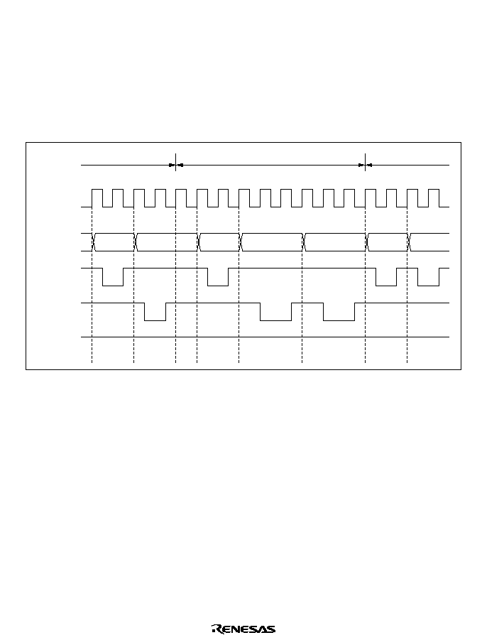
235
7.4.8
DMAC Bus Cycle
Figure 7.13 shows an example of the timing of the basic DMAC bus cycle. This example shows a
word-size transfer from a 16-bit two-state access area to an 8-bit three-state access area. When the
DMAC gets the bus from the CPU, after one dead cycle (T
d
), it reads from the source address and
writes to the destination address. During these read and write operations the bus is not released
even if there is another bus request. DMAC cycles comply with bus controller settings in the same
way as CPU cycles.
RD
HWR
LWR
T
1
T
2
T
1
T
2
T
d
T
1
T
2
T
1
T
2
T
3
T
1
T
2
T
3
T
1
T
2
T
1
T
2
CPU cycle
DMAC cycle (1 word transfer)
CPU cycle
Source
address
Destination address
Address
bus
Figure 7.13 DMA Transfer Bus Timing (Example)
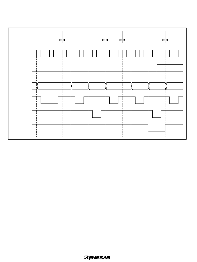
236
Figure 7.14 shows the timing when the DMAC is activated by low input at a
DREQ pin. This
example shows a word-size transfer from a 16-bit two-state access area to another 16-bit two-state
access area. The DMAC continues the transfer while the
DREQ pin is held low.
DREQ
RD
HWR
TEND
T
1
T
2
T
3
T
d
T
1
T
2
T
1
T
2
T
1
T
2
T
d
T
1
T
2
T
1
T
2
T
1
T
2
LWR
,
CPU cycle
DMAC cycle
CPU cycle
DMAC cycle
(last transfer cycle)
CPU cycle
Source
address
Destination
address
Source
address
Destination
address
Address
bus
Figure 7.14 Bus Timing of DMA Transfer Requested by Low
DREQ Input
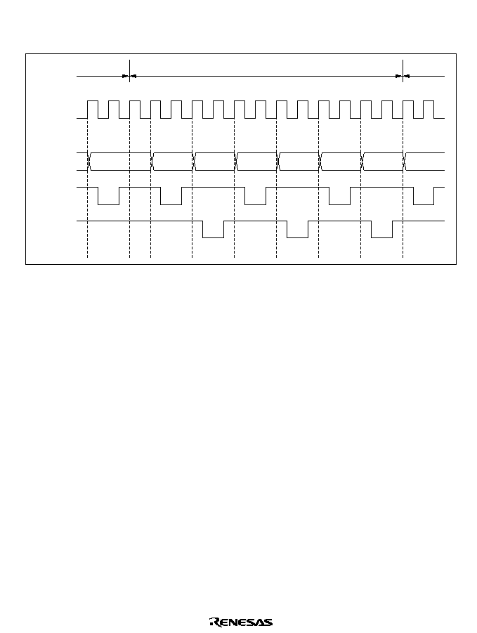
237
Figure 7.15 shows an auto-requested burst-mode transfer. This example shows a transfer of three
words from a 16-bit two-state access area to another 16-bit two-state access area.
T
1
T
2
T
1
T
2
T
1
T
2
T
1
T
2
T
1
T
2
T
1
T
2
T
1
T
2
T
1
T
2
RD
,
CPU cycle
DMAC cycle
Source
address
Destination
address
CPU cycle
T
d
Address
bus
HWR
LWR
Figure 7.15 Burst DMA Bus Timing
When the DMAC is activated from a
DREQ pin there is a minimum interval of four states from
when the transfer is requested until the DMAC starts operating. The
DREQ pin is not sampled
during the time between the transfer request and the start of the transfer. In short address mode and
normal mode, the pin is next sampled at the end of the read cycle. In block transfer mode, the pin
is next sampled at the end of one block transfer.
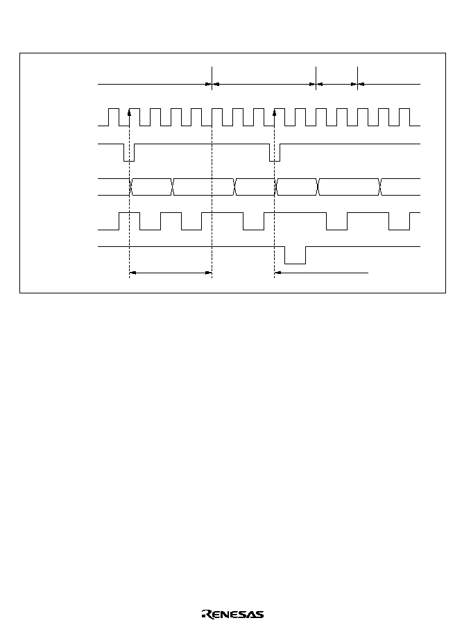
238
Figure 7.16 shows the timing when the DMAC is activated by the falling edge of
DREQ in normal
mode.
DREQ
RD
HWR
T
2
T
1
T
2
T
1
T
2
T
d
T
1
T
2
T
1
T
2
T
1
T
2
T
d
T
1
T
2
LWR
,
CPU cycle
DMAC cycle
CPU
cycle
DMAC cycle
Minimum 4 states
Next sampling point
Address
bus
Figure 7.16 Timing of DMAC Activation by Falling Edge of
DREQ in Normal Mode
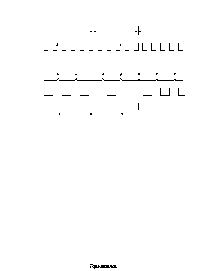
239
Figure 7.17 shows the timing when the DMAC is activated by level-sensitive low
DREQ input in
normal mode.
DREQ
RD
HWR
LWR
,
T
2
T
1
T
2
T
1
T
2
T
d
T
1
T
2
T
1
T
2
T
1
T
2
T
1
T
2
T
1
CPU cycle
DMAC cycle
CPU cycle
Minimum 4 states
Next sampling point
Address
bus
Figure 7.17 Timing of DMAC Activation by Low
DREQ Level in Normal Mode
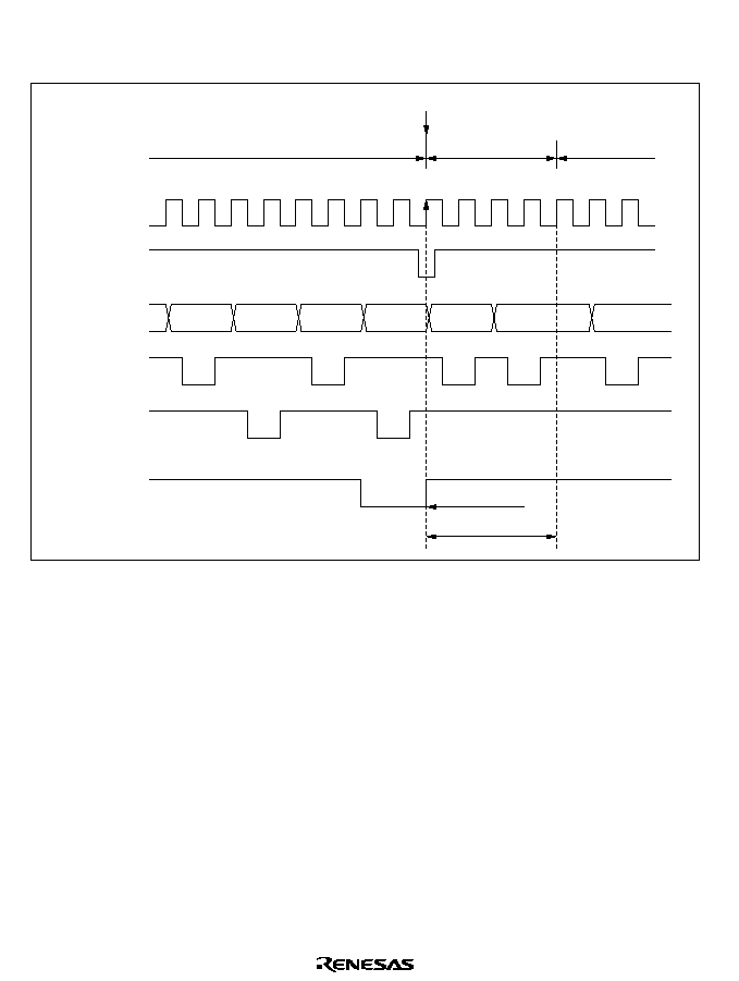
240
Figure 7.18 shows the timing when the DMAC is activated by the falling edge of
DREQ in block
transfer mode.
DREQ
RD
HWR
TEND
T
1
T
2
T
1
T
2
T
1
T
2
T
1
T
2
T
1
T
2
T
1
T
2
T
d
T
1
T
2
DMAC cycle
DMAC cycle
CPU cycle
Next sampling
Minimum 4 states
End of 1 block transfer
LWR
,
Address
bus
Figure 7.18 Timing of DMAC Activation by Falling Edge of
DREQ in Block Transfer Mode
241
7.4.9
Multiple-Channel Operation
The DMAC channel priority order is: channel 0 > channel 1 and channel A > channel B.
Table 7.12 shows the complete priority order.
Table 7.12
Channel Priority Order
Short Address Mode
Full Address Mode
Priority
Channel 0A
Channel 0
High
Channel 0B
Channel 1A
Channel 1
Channel 1B
Low
If transfers are requested on two or more channels simultaneously, or if a transfer on one channel
is requested during a transfer on another channel, the DMAC operates as follows.
�
When a transfer is requested, the DMAC requests the bus right. When it gets the bus right, it
starts a transfer on the highest-priority channel at that time.
�
Once a transfer starts on one channel, requests to other channels are held pending until that
channel releases the bus.
�
After each transfer in short address mode, and each externally-requested or cycle-steal transfer
in normal mode, the DMAC releases the bus and returns to step 1. After releasing the bus, if
there is a transfer request for another channel, the DMAC requests the bus again.
�
After completion of a burst-mode transfer, or after transfer of one block in block transfer
mode, the DMAC releases the bus and returns to step 1. If there is a transfer request for a
higher-priority channel or a bus request from a higher-priority bus master, however, the
DMAC releases the bus after completing the transfer of the current byte or word. After
releasing the bus, if there is a transfer request for another channel, the DMAC requests the bus
again.
Figure 7.19 shows the timing when channel 0A is set up for I/O mode and channel 1 for burst
mode, and a transfer request for channel 0A is received while channel 1 is active.
242
RD
T
1
T
2
T
1
T
2
T
d
T
1
T
2
T
1
T
2
T
1
T
2
T
d
T
1
T
2
T
1
T
2
,
DMAC cycle
(channel 1)
CPU
cycle
DMAC cycle
(channel 0A)
CPU
cycle
DMAC cycle
(channel 1)
Address
bus
HWR
LWR
Figure 7.19 Timing of Multiple-Channel Operations
7.4.10
External Bus Requests, DRAM Interface, and DMAC
During a DMAC transfer, if the bus right is requested by an external bus request signal (
BREQ) or
by the DRAM interface (refresh cycle), the DMAC releases the bus after completing the transfer
of the current byte or word. If there is a transfer request at this point, the DMAC requests the bus
right again. Figure 7.20 shows an example of the timing of insertion of a refresh cycle during a
burst transfer on channel 0.
RD
HWR LWR
,
T
1
T
2
T
1
T
2
T
1
T
2
T
1
T
2
T
1
T
2
T
d
T
1
T
2
T
1
T
2
T
1
T
2
DMAC cycle (channel 0)
DMAC cycle (channel 0)
Refresh
cycle
Address
bus
Figure 7.20 Bus Timing of DRAM Interface, and DMAC
243
7.4.11
NMI Interrupts and DMAC
NMI interrupts do not affect DMAC operations in short address mode.
If an NMI interrupt occurs during a transfer in full address mode, the DMAC suspends operations.
In full address mode, a channel is enabled when its DTE and DTME bits are both set to 1. NMI
input clears the DTME bit to 0. After transferring the current byte or word, the DMAC releases the
bus to the CPU. In normal mode, the suspended transfer resumes when the CPU sets the DTME
bit to 1 again. Check that the DTE bit is set to 1 and the DTME bit is cleared to 0 before setting
the DTME bit to 1.
Figure 7.21 shows the procedure for resuming a DMAC transfer in normal mode on channel 0
after the transfer was halted by NMI input.
Resuming DMAC transfer
in normal mode
DTE = 1
DTME = 0
Set DTME to 1
DMA transfer continues
End
1.
2.
Check that DTE = 1 and DTME = 0.
Read DTCRB while DTME = 0,
then write 1 in the DTME bit.
2
No
Yes
1
Figure 7.21 Procedure for Resuming a DMAC Transfer Halted by NMI (Example)
For information about NMI interrupts in block transfer mode, see section 7.6.6, NMI Interrupts
and Block Transfer Mode.
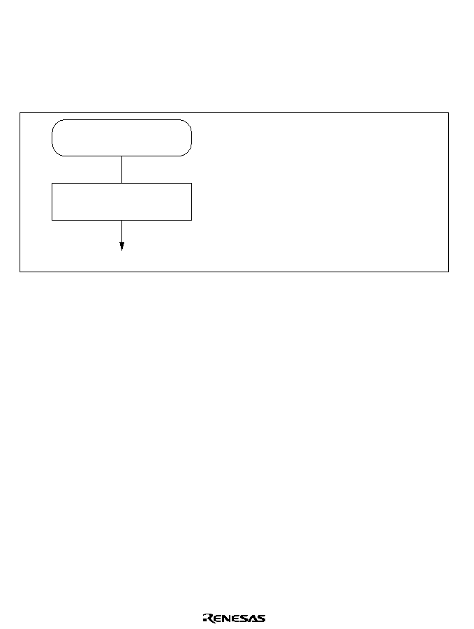
244
7.4.12
Aborting a DMAC Transfer
When the DTE bit in an active channel is cleared to 0, the DMAC halts after transferring the
current byte or word. The DMAC starts again when the DTE bit is set to 1. In full address mode,
the DTME bit can be used for the same purpose. Figure 7.22 shows the procedure for aborting a
DMAC transfer by software.
DMAC transfer abort
Set DTCR
DMAC transfer aborted
1
1. Clear the DTE bit to 0 in DTCR.
To avoid generating an interrupt when
aborting a DMAC transfer, clear the DTIE
bit to 0 simultaneously.
Figure 7.22 Procedure for Aborting a DMAC Transfer
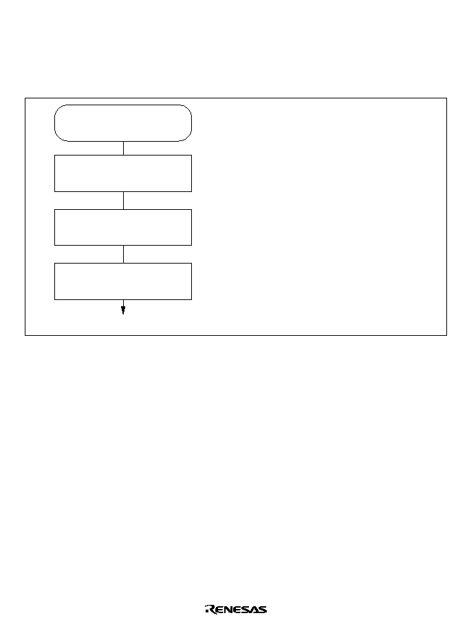
245
7.4.13
Exiting Full Address Mode
Figure 7.23 shows the procedure for exiting full address mode and initializing the pair of channels.
To set the channels up in another mode after exiting full address mode, follow the setup procedure
for the relevant mode.
Exiting full address mode
Halt the channel
Initialize DTCRB
Initialize DTCRA
Initialized and halted
1
2
3
1.
2.
3.
Clear the DTE bit to 0 in DTCRA, or wait
for the transfer to end and the DTE bit
to be cleared to 0.
Clear all DTCRB bits to 0.
Clear all DTCRA bits to 0.
Figure 7.23 Procedure for Exiting Full Address Mode (Example)
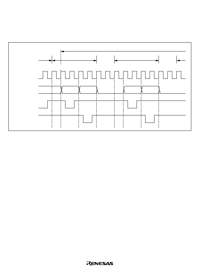
246
7.4.14
DMAC States in Reset State, Standby Modes, and Sleep Mode
When the chip is reset or enters software standby mode, the DMAC is initialized and halts. DMAC
operations continue in sleep mode. Figure 7.24 shows the timing of a cycle-steal transfer in sleep
mode.
Address bus
RD
HWR LWR
,
2
T
d
T
T
2
1
T
2
T
d
T
1
T
2
T
1
T
2
T
1
T
CPU cycle
DMAC cycle
DMAC cycle
Sleep mode
d
T
Figure 7.24 Timing of Cycle-Steal Transfer in Sleep Mode
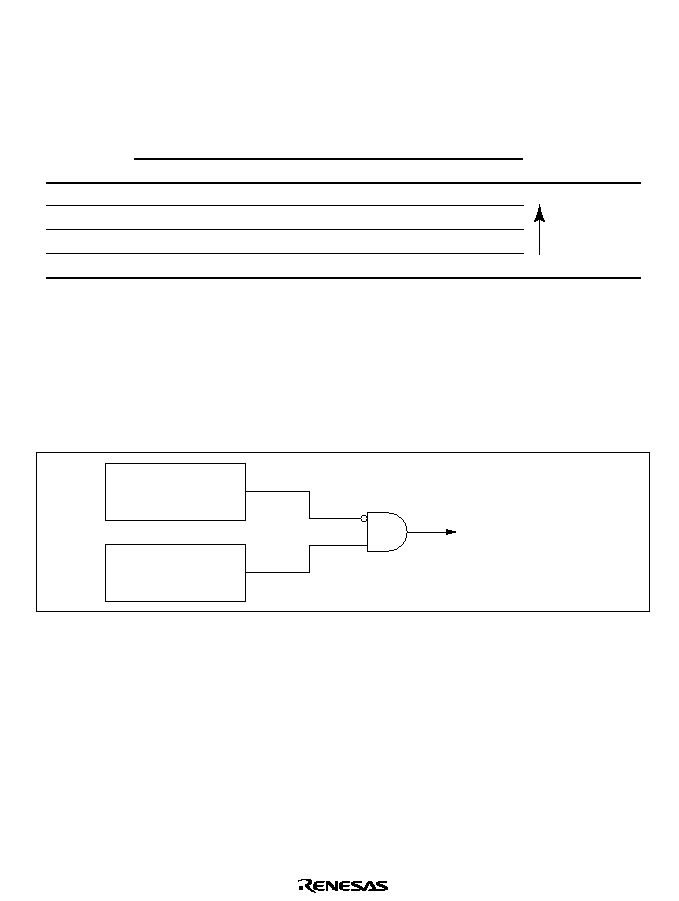
247
7.5
Interrupts
The DMAC generates only DMA-end interrupts. Table 7.13 lists the interrupts and their priority.
Table 7.13
DMAC Interrupts
Description
Interrupt
Short Address Mode
Full Address Mode
Interrupt Priority
DEND0A
End of transfer on channel 0A
End of transfer on channel 0
High
DEND0B
End of transfer on channel 0B
--
DEND1A
End of transfer on channel 1A
End of transfer on channel 1
DEND1B
End of transfer on channel 1B
--
Low
Each interrupt is enabled or disabled by the DTIE bit in the corresponding data transfer control
register (DTCR). Separate interrupt signals are sent to the interrupt controller.
The interrupt priority order among channels is channel 0 > channel 1 and channel A > channel B.
Figure 7.25 shows the DMA-end interrupt logic. An interrupt is requested whenever DTE = 0 and
DTIE = 1.
DTE
DTIE
DMA-end interrupt
Figure 7.25 DMA-End Interrupt Logic
The DMA-end interrupt for the B channels (DENDB) is unavailable in full address mode. The
DTME bit does not affect interrupt operations.

248
7.6
Usage Notes
7.6.1
Note on Word Data Transfer
Word data cannot be accessed starting at an odd address. When word-size transfer is selected, set
even values in the memory and I/O address registers (MAR and IOAR).
7.6.2
DMAC Self-Access
The DMAC itself cannot be accessed during a DMAC cycle. DMAC registers cannot be specified
as source or destination addresses.
7.6.3
Longword Access to Memory Address Registers
A memory address register can be accessed as longword data at the MARR address.
Example
MOV.L
#LBL, ER0
MOV.L
ER0, @MARR
Four byte accesses are performed. Note that the CPU may release the bus between the second byte
(MARE) and third byte (MARH).
Memory address registers should be written and read only when the DMAC is halted.
7.6.4
Note on Full Address Mode Setup
Full address mode is controlled by two registers: DTCRA and DTCRB. Care must be taken to
prevent the B channel from operating in short address mode during the register setup. The enable
bits (DTE and DTME) should not be set to 1 until the end of the setup procedure.
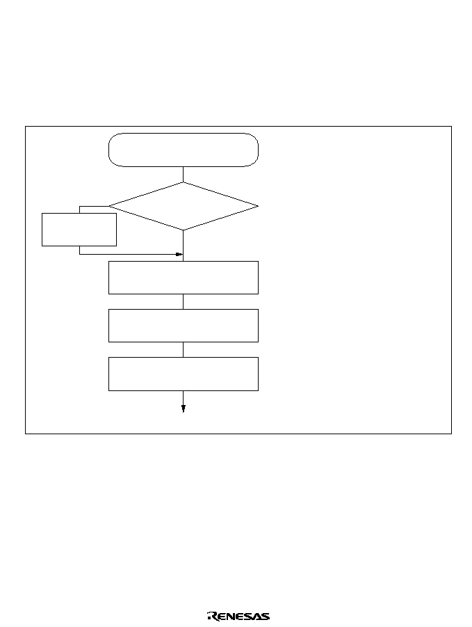
249
7.6.5
Note on Activating DMAC by Internal Interrupts
When using an internal interrupt to activate the DMAC, make sure that the interrupt selected as
the activating source does not occur during the interval after it has been selected but before the
DMAC has been enabled. The on-chip supporting module that will generate the interrupt should
not be activated until the DMAC has been enabled. If the DMAC must be enabled while the on-
chip supporting module is active, follow the procedure in figure 7.26.
Enabling of DMAC
Selected interrupt
requested?
Interrupt hand-
ling by CPU
Clear selected interrupt's
enable bit to 0
Enable DMAC
Set selected interrupt's
enable bit to 1
1
2
3
4
1.
2.
3.
4.
While the DTE bit is cleared to 0,
interrupt requests are sent to the
CPU.
Clear the interrupt enable bit to 0
in the interrupt-generating on-chip
supporting module.
Enable the DMAC.
Enable the DMAC-activating
interrupt.
DMAC operates
Yes
No
Figure 7.26 Procedure for Enabling DMAC while On-Chip Supporting
Module is Operating (Example)
If the DTE bit is set to 1 but the DTME bit is cleared to 0, the DMAC is halted and the selected
activating source cannot generate a CPU interrupt. If the DMAC is halted by an NMI interrupt, for
example, the selected activating source cannot generate CPU interrupts. To terminate DMAC
operations in this state, clear the DTE bit to 0 to allow CPU interrupts to be requested. To continue
DMAC operations, carry out steps 2 and 4 in figure 7.26 before and after setting the DTME bit
to 1.

250
When 16-bit timer interrupt activates the DMAC, make sure the next interrupt does not occur
before the DMA transfer ends. If one 16-bit timer interrupt activates two or more channels, make
sure the next interrupt does not occur before the DMA transfers end on all the activated channels.
If the next interrupt occurs before a transfer ends, the channel or channels for which that interrupt
was selected may fail to accept further activation requests.
7.6.6
NMI Interrupts and Block Transfer Mode
If an NMI interrupt occurs in block transfer mode, the DMAC operates as follows.
�
When the NMI interrupt occurs, the DMAC finishes transferring the current byte or word, then
clears the DTME bit to 0 and halts. The halt may occur in the middle of a block.
It is possible to find whether a transfer was halted in the middle of a block by checking the
block size counter. If the block size counter does not have its initial value, the transfer was
halted in the middle of a block.
�
If the transfer is halted in the middle of a block, the activating interrupt flag is cleared to 0. The
activation request is not held pending.
�
While the DTE bit is set to 1 and the DTME bit is cleared to 0, the DMAC is halted and does
not accept activating interrupt requests. If an activating interrupt occurs in this state, the
DMAC does not operate and does not hold the transfer request pending internally. Neither is a
CPU interrupt requested.
For this reason, before setting the DTME bit to 1, first clear the enable bit of the activating
interrupt to 0. Then, after setting the DTME bit to 1, set the interrupt enable bit to 1 again. See
section 7.6.5, Note on Activating DMAC by Internal Interrupts.
�
When the DTME bit is set to 1, the DMAC waits for the next transfer request. If it was halted
in the middle of a block transfer, the rest of the block is transferred when the next transfer
request occurs. Otherwise, the next block is transferred when the next transfer request occurs.
7.6.7
Memory and I/O Address Register Values
Table 7.14 indicates the address ranges that can be specified in the memory and I/O address
registers (MAR and IOAR).
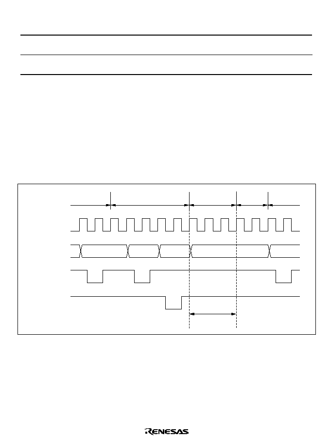
251
Table 7.14
Address Ranges Specifiable in MAR and IOAR
1-Mbyte Mode
16-Mbyte Mode
MAR
H'00000 to H'FFFFF
(0 to 1048575)
H'000000 to H'FFFFFF
(0 to 16777215)
IOAR
H'FFF00 to H'FFFFF
(1048320 to 1048575)
H'FFFF00 to H'FFFFFF
(16776960 to 16777215)
MAR bits 23 to 20 are ignored in 1-Mbyte mode.
7.6.8
Bus Cycle when Transfer is Aborted
When a transfer is aborted by clearing the DTE bit or suspended by an NMI that clears the DTME
bit, if this halts a channel for which the DMAC has a transfer request pending internally, a dead
cycle may occur. This dead cycle does not update the halted channel's address register or counter
value. Figure 7.27 shows an example in which an auto-requested transfer in cycle-steal mode on
channel 0 is aborted by clearing the DTE bit in channel 0.
Address bus
RD
HWR
,
LWR
CPU cycle
DMAC cycle
CPU cycle
DMAC
cycle
CPU cycle
DTE bit is
cleared
T
1
T
2
T
d
T
1
T
2
T
1
T
2
T
1
T
2
T
3
T
d
T
d
T
1
T
2
Figure 7.27 Bus Timing at Abort of DMA Transfer in Cycle-Steal Mode
7.6.9
Transfer Requests by A/D Converter
When the A/D converter is set to scan mode and conversion is performed on more than one
channel, the A/D converter generates a transfer request when all conversions are completed. The
converted data is stored in the appropriate ADDR registers. Block transfer mode and full address
mode should therefore be used to transfer all the conversion results at one time.

252

253
Section 8 I/O Ports
8.1
Overview
This LSI has ten input/output ports (ports 1 to 6, 8, 9, A, and B) and one input port (port 7). Table
8.1 summarizes the port functions. The pins in each port are multiplexed as shown in table 8.1.
Each port has a data direction register (DDR) for selecting input or output, and a data register
(DR) for storing output data. In addition to these registers, ports 2, 4, and 5 have an input pull-up
control register (PCR) for switching input pull-up transistors on and off.
Ports 1 to 6 and port 8 can drive one TTL load and a 90-pF capacitive load. Ports 9, A, and B can
drive one TTL load and a 30-pF capacitive load. Ports 1 to 6 and 8 to B can drive a darlington
pair. Ports 1, 2, and 5 can drive LEDs (with 10-mA current sink). Pins P8
2
to P8
0
, PA
7
to PA
0
have
Schmitt-trigger input circuits.
For block diagrams of the ports see appendix C, I/O Port Block Diagrams.

254
Table 8.1
Port Functions
Expanded Modes
Single-Chip Modes
Port
Description
Pins
Mode 1
Mode 2
Mode 3
Mode 4 Mode 5
Mode 7
Port 1
�
8-bit I/O port
�
Can drive LEDs
P1
7
to P1
0
/
A
7
to A
0
Address output pins (A
7
to A
0
)
Address output (A
7
to
A
0
) and generic input
DDR = 0:
generic input
DDR = 1:
address output
Generic input/output
Port 2
�
8-bit I/O port
�
Built-in input pull-
up transistors
�
Can drive LEDs
P2
7
to P2
0
/
A
15
to A
8
Address output pins (A
15
to A
8
)
Address output (A
15
to
A
8
) and generic input
DDR = 0:
generic input
DDR = 1:
address output
Generic input/output
Port 3
�
8-bit I/O port
P3
7
to P3
0
/
D
15
to D
8
Data input/output (D
15
to D
8
)
Generic input/output
Port 4
�
8-bit I/O port
�
Built-in input pull-
up transistors
P4
7
to P4
0
/
D
7
to D
0
Data input/output (D
7
to D
0
) and 8-bit generic input/output
8-bit bus mode: generic input/output
16-bit bus mode: data input/output
Generic input/output
Port 5
�
4-bit I/O port
�
Built-in input pull-
up transistors
�
Can drive LEDs
P5
3
to P5
0
/
A
19
to A
16
Address output (A
19
to A
16
)
Address output (A
19
to
A
16
) and 4-bit
generic input
DDR = 0: generic input
DDR = 1: address output
Generic input/output
Port 6
�
7-bit I/O port and
1-bit input port
P6
7
/
Clock output (
) and generic input
P6
6
/
LWR
P6
5
/
HWR
P6
4
/
RD
P6
3
/
AS
Bus control signal output (
LWR
,
HWR
,
RD
,
AS
)
Generic input/output
P6
2
/
BACK
P6
1
/
BREQ
P6
0
/
WAIT
Bus control signal input/output (
BACK
,
BREQ
,
WAIT
) and
3-bit generic input/output
Port 7
�
8-bit input port
P7
7
/AN
7
/DA
1
P7
6
/AN
6
/DA
0
Analog input (AN
7
, AN
6
) to A/D converter, analog output (DA
1
, DA
0
)
from D/A converter, and generic input
P7
5
to P7
0
/
AN
5
to AN
0
Analog input (AN
5
to AN
0
) to A/D converter, and generic input
Port 8
�
5-bit I/O port
�
P8
2
to P8
0
have
Schmitt inputs
P8
4
/
CS
0
DDR = 0: generic input
DDR = 1 (reset value):
CS
0
output
DDR = 0 (reset value):
generic input
DDR = 1:
CS
0
output
Generic input/output
P8
3
/
IRQ
3
/
CS
1
/
ADTRG
IRQ
3
input,
CS
1
output, external trigger input (
ADTRG
) to A/D converter,
and generic input
DDR = 0 (after reset): generic input
DDR = 1:
CS
1
output
IRQ
3
input, external trigger
input (
ADTRG
) to A/D
converter, and generic
input/output
P8
2
/
IRQ
2
/
CS
2
P8
1
/
IRQ
1
/
CS
3
IRQ
2
and
IRQ
1
input,
CS
2
and
CS
3
output, and generic input
*
DDR = 0 (reset value): generic input
DDR = 1:
CS
2
and
CS
3
output
IRQ
2
and
IRQ
1
input and
generic input/output
P8
0
/
IRQ
0
/
RFSH
IRQ
0
input,
RFSH
output, and generic input/output
IRQ
0
input and generic
input/output
Note:
*
P8
1
can be used as an output port by making a setting in DRCRA.

255
Expanded Modes
Single-Chip Modes
Port
Description
Pins
Mode 1
Mode 2
Mode 3
Mode 4
Mode 5
Mode 7
Port 9
�
6-bit I/O port
P9
5
/
IRQ
5
/SCK
1
P9
4
/
IRQ
4
/SCK
0
P9
3
/RxD
1
P9
2
/RxD
0
P9
1
/TxD
1
P9
0
/TxD
0
Input and output (SCK
1
, SCK
0
, RxD
1
, RxD
0
, TxD
1
, TxD
0
) for serial communication interfaces 1 and 0
(SCI1/0),
IRQ
5
and
IRQ
4
input, and 6-bit generic input/output
Port A
�
8-bit I/O port
�
Schmitt inputs
PA
7
/TP
7
/
TIOCB
2
/A
20
Output (TP
7
) from pro-
grammable timing
pattern controller (TPC),
input or output (TIOCB
2
)
for 16-bit timer and
generic input/output
Address output
(A
20
)
Address output (A
20
),
TPC output (TP
7
), input
or output (TIOCB
2
) for
16-bit timer, and
generic input/output
TPC output (TP
7
), 16-bit
timer input or output
(TIOCB
2
), and generic
input/output
PA
6
/TP
6
/
TIOCA
2
/A
21
PA
5
/TP
5
/
TIOCB
1
/A
22
PA
4
/TP
4
/
TIOCA
1
/A
23
TPC output (TP
6
to TP
4
),
16-bit timer input and
output (TIOCA
2
, TIOCB
1
,
TIOCA
1
) , and generic
input/output
TPC output (TP
6
to TP
4
),16-bit timer input and
output (TIOCA
2
, TIOCB
1
, TIOCA
1
), address
output (A
23
to A
21
), and generic input/output
TPC output (TP
6
to TP
4
),
16-bit timer input and
output (TIOCA
2
, TIOCB
1
,
TIOCA
1
) and generic
input/output
PA
3
/TP
3
/
TIOCB
0
/
TCLKD
PA
2
/TP
2
/
TIOCA
0
/
TCLKC
PA
1
/TP
1
/
TCLKB
/
TEND
1
PA
0
/TP
0
/
TCLKA
/
TEND
0
TPC output (TP
3
to TP
0
), 16-bit timer input and output (TIOCB
0
, TIOCA
0
, TCLKD, TCLKC, TCLKB,
TCLKA), 8-bit timer input (TCLKD, TCLKC, TCLKB, TCLKA), output (
TEND
1
,
TEND
0
) from DMA
controller (DMAC), and generic input/output
Port B
�
8-bit I/O port
PB
7
/TP
15
/
RXD
2
PB
6
/TP
14
/
TXD
2
PB
5
/TP
13
/
SCK
2
/
LCAS
PB
4
/TP
12
/
UCAS
TPC output (TP
15
to TP
12
), SCI2 input and output (SCK
2
, RxD
2
, TxD
2
), DRAM
interface output (
LCAS
,
UCAS
), and generic input/output
TPC output (TP
15
to
TP
12
), SCI2 input and
output (SCK
2
, RxD
2
,
TxD
2
), and generic
input/output
PB
3
/TP
11
/
TMIO
3
/
DREQ
1
/
CS
4
PB
2
/TP
10
/
TMO
2
/
CS
5
PB
1
/TP
9
/
TMIO
1
/
DREQ
0
/
CS
6
PB
0
/TP
8
/
TMO
0
/
CS
7
TPC output (TP
11
to TP
8
), 8-bit timer input and output (TMIO
3
, TMO
2
, TMIO
1
,
TMO
0
), DMAC input (
DREQ
1
,
DREQ
0
),
CS
7
to
CS
4
output, and generic
input/output
TPC output (TP
11
to TP
8
),
8-bit timer input and
output (TMIO
3
, TMO
2
,
TMIO
1
, TMO
0
), DMAC
input (
DREQ
1
,
DREQ
0
),
and generic input/output
256
8.2
Port 1
8.2.1
Overview
Port 1 is an 8-bit input/output port also used for address output, with the pin configuration shown
in figure 8.1. The pin functions differ between the expanded modes with on-chip ROM disabled,
expanded modes with on-chip ROM enabled, and single-chip mode. In modes 1 to 4 (expanded
modes with on-chip ROM disabled), they are address bus output pins (A
7
to A
0
).
In mode 5 (expanded mode with on-chip ROM enabled), settings in the port 1 data direction
register (P1DDR) can designate pins for address bus output (A
7
to A
0
) or generic input. In mode 7
(single-chip mode), port 1 is a generic input/output port.
When DRAM is connected to areas 2 to 5, A
7
to A
0
output row and column addresses in read and
write cycles. For details see section 6.5, DRAM Interface.
Pins in port 1 can drive one TTL load and a 90-pF capacitive load. They can also drive an LED or
a darlington transistor pair.
Port 1
P1 /A
P1 /A
P1 /A
P1 /A
P1 /A
P1 /A
P1 /A
P1 /A
7
6
5
4
3
2
1
0
7
6
5
4
3
2
1
0
P1 (input/output)
P1 (input/output)
P1 (input/output)
P1 (input/output)
P1 (input/output)
P1 (input/output)
P1 (input/output)
P1 (input/output)
7
6
5
4
3
2
1
0
A (output)
A (output)
A (output)
A (output)
A (output)
A (output)
A (output)
A (output)
7
6
5
4
3
2
1
0
Port 1 pins
Mode 7
Modes 1 to 4
P1 (input)/A (output)
P1 (input)/A (output)
P1 (input)/A (output)
P1 (input)/A (output)
P1 (input)/A (output)
P1 (input)/A (output)
P1 (input)/A (output)
P1 (input)/A (output)
7
6
5
4
3
2
1
0
Mode 5
7
6
5
4
3
2
1
0
Figure 8.1 Port 1 Pin Configuration
257
8.2.2
Register Descriptions
Table 8.2 summarizes the registers of port 1.
Table 8.2
Port 1 Registers
Initial Value
Address
*
Name
Abbreviation R/W
Modes 1 to 4
Modes 5 and 7
H'EE000
Port 1 data direction register
P1DDR
W
H'FF
H'00
H'FFFD0
Port 1 data register
P1DR
R/W
H'00
H'00
Note:
*
Lower 20 bits of the address in advanced mode.
Port 1 Data Direction Register (P1DDR): P1DDR is an 8-bit write-only register that can select
input or output for each pin in port 1.
Bit
Modes
1 to 4
Initial value
Read/Write
Initial value
Read/Write
Modes
5 and 7
7
P1 DDR
1
--
0
W
7
6
P1 DDR
1
--
0
W
6
5
P1 DDR
1
--
0
W
5
4
P1 DDR
1
--
0
W
4
3
P1 DDR
1
--
0
W
3
2
P1 DDR
1
--
0
W
2
1
P1 DDR
1
--
0
W
1
0
P1 DDR
1
--
0
W
0
Port 1 data direction 7 to 0
These bits select input or
output for port 1 pins
Modes 1 to 4 (Expanded Modes with On-Chip ROM Disabled): P1DDR values are fixed at 1.
Port 1 functions as an address bus.
Mode 5 (Expanded Mode with On-Chip ROM Enabled): After a reset, port 1 functions as an
input port. A pin in port 1 becomes an address output pin if the corresponding P1DDR bit is set to
1, and a generic input pin if this bit is cleared to 0.
Mode 7 (Single-Chip Mode): Port 1 functions as an input/output port. A pin in port 1 becomes an
output port if the corresponding P1DDR bit is set to 1, and an input port if this bit is cleared to 0.

258
In modes 1 to 4, P1DDR bits are always read as 1, and cannot be modified.
In modes 5 and 7, P1DDR is a write-only register. Its value cannot be read. All bits return 1 when
read.
P1DDR is initialized to H'FF in modes 1 to 4, and to H'00 in modes 5 and 7, by a reset and in
hardware standby mode. In software standby mode it retains its previous setting. Therefore, if a
transition is made to software standby mode while port 1 is functioning as an input/output port and
a P1DDR bit is set to 1, the corresponding pin maintains its output state.
Port 1 Data Register (P1DR): P1DR is an 8-bit readable/writable register that stores port 1
output data. When port 1 functions as an output port, the value of this register is output. When
this register is read, the pin logic level is read for bits for which the P1DDR setting is 0, and the
P1DR value is read for bits for which the P1DDR setting is 1.
Bit
Initial value
Read/Write
7
P1
0
R/W
Port 1 data 7 to 0
These bits store data for port 1 pins
7
6
P1
0
R/W
6
5
P1
0
R/W
5
4
P1
0
R/W
4
3
P1
0
R/W
3
2
P1
0
R/W
2
1
P1
0
R/W
1
0
P1
0
R/W
0
P1DR is initialized to H'00 by a reset and in hardware standby mode. In software standby mode it
retains its previous setting.
259
8.3
Port 2
8.3.1
Overview
Port 2 is an 8-bit input/output port also used for address output, with the pin configuration shown
in figure 8.2. The pin functions differ according to the operating mode.
In modes 1 to 4 (expanded modes with on-chip ROM disabled), port 2 consists of address bus
output pins (A
15
to A
8
). In mode 5 (expanded mode with on-chip ROM enabled), settings in the
port 2 data direction register (P2DDR) can designate pins for address bus output (A
15
to A
8
) or
generic input. In mode 7 (single-chip mode), port 2 is a generic input/output port.
When DRAM is connected to areas 2 to 5, A
12
to A
8
output row and column addresses in read and
write cycles. For details see section 6.5, DRAM Interface.
Port 2 has software-programmable built-in pull-up transistors.
Pins in port 2 can drive one TTL load and a 90-pF capacitive load. They can also drive an LED or
a darlington transistor pair.
Port 2
P2 /A
P2 /A
P2 /A
P2 /A
P2 /A
P2 /A
P2 /A
P2 /A
7
6
5
4
3
2
1
0
15
14
13
12
11
10
9
8
P2 (input/output)
P2 (input/output)
P2 (input/output)
P2 (input/output)
P2 (input/output)
P2 (input/output)
P2 (input/output)
P2 (input/output)
7
6
5
4
3
2
1
0
A (output)
A (output)
A (output)
A (output)
A (output)
A (output)
A (output)
A (output)
15
14
13
12
11
10
9
8
Port 2 pins
Mode 7
Modes 1 to 4
P2 (input)/A (output)
P2 (input)/A (output)
P2 (input)/A (output)
P2 (input)/A (output)
P2 (input)/A (output)
P2 (input)/A (output)
P2 (input)/A (output)
P2 (input)/A (output)
7
6
5
4
3
2
1
0
Mode 5
15
14
13
12
11
10
9
8
Figure 8.2 Port 2 Pin Configuration
260
8.3.2
Register Descriptions
Table 8.3 summarizes the registers of port 2.
Table 8.3
Port 2 Registers
Initial Value
Address
*
Name
Abbreviation R/W Modes 1 to 4 Modes 5 and 7
H'EE001
Port 2 data direction register
P2DDR
W
H'FF
H'00
H'FFFD1
Port 2 data register
P2DR
R/W H'00
H'00
H'EE03C
Port 2 input pull-up MOS control
register
P2PCR
R/W H'00
H'00
Note:
*
Lower 20 bits of the address in advanced mode.
Port 2 Data Direction Register (P2DDR): P2DDR is an 8-bit write-only register that can select
input or output for each pin in port 2.
Bit
Modes
1 to 4
Initial value
Read/Write
Initial value
Read/Write
Modes
5 and 7
7
P2 DDR
1
--
0
W
7
6
P2 DDR
1
--
0
W
6
5
P2 DDR
1
--
0
W
5
4
P2 DDR
1
--
0
W
4
3
P2 DDR
1
--
0
W
3
2
P2 DDR
1
--
0
W
2
1
P2 DDR
1
--
0
W
1
0
P2 DDR
1
--
0
W
0
Port 2 data direction 7 to 0
These bits select input or
output for port 2 pins
Modes 1 to 4 (Expanded Modes with On-Chip ROM Disabled): P2DDR values are fixed at 1.
Port 2 functions as an address bus.
Mode 5 (Expanded Mode with On-Chip ROM Enabled): Following a reset, port 2 is an input
port. A pin in port 2 becomes an address output pin if the corresponding P2DDR bit is set to 1, and
a generic input port if this bit is cleared to 0.
Mode 7 (Single-Chip Mode): Port 2 functions as an input/output port. A pin in port 2 becomes an
output port if the corresponding P2DDR bit is set to 1, and an input port if this bit is cleared to 0.
261
In modes 1 to 4, P2DDR bits are always read as 1, and cannot be modified.
In modes 5 and 7, P2DDR is a write-only register. Its value cannot be read. All bits return 1 when
read.
P2DDR is initialized to H'FF in modes 1 to 4, and to H'00 in modes 5 and 7, by a reset and in
hardware standby mode. In software standby mode it retains its previous setting. Therefore, if a
transition is made to software standby mode while port 2 is functioning as an input/output port and
a P2DDR bit is set to 1, the corresponding pin maintains its output state.
Port 2 Data Register (P2DR): P2DR is an 8-bit readable/writable register that stores output data
for port 2. When port 2 functions as an output port, the value of this register is output. When a bit
in P2DDR is set to 1, if port 2 is read the value of the corresponding P2DR bit is returned. When a
bit in P2DDR is cleared to 0, if port 2 is read the corresponding pin logic level is read.
Bit
Initial value
Read/Write
7
P2
0
R/W
Port 2 data 7 to 0
These bits store data for port 2 pins
7
6
P2
0
R/W
6
5
P2
0
R/W
5
4
P2
0
R/W
4
3
P2
0
R/W
3
2
P2
0
R/W
2
1
P2
0
R/W
1
0
P2
0
R/W
0
P2DR is initialized to H'00 by a reset and in hardware standby mode. In software standby mode it
retains its previous setting.
Port 2 Input Pull-Up MOS Control Register (P2PCR): P2PCR is an 8-bit readable/writable
register that controls the MOS input pull-up transistors in port 2.
Bit
Initial value
Read/Write
7
P2 PCR
0
R/W
Port 2 input pull-up MOS control 7 to 0
These bits control input pull-up
transistors built into port 2
7
6
P2 PCR
0
R/W
6
5
P2 PCR
0
R/W
5
4
P2 PCR
0
R/W
4
3
P2 PCR
0
R/W
3
2
P2 PCR
0
R/W
2
1
P2 PCR
0
R/W
1
0
P2 PCR
0
R/W
0
In modes 5 and 7, when a P2DDR bit is cleared to 0 (selecting generic input), if the corresponding
bit in P2PCR is set to 1, the input pull-up transistor is turned on.
P2PCR is initialized to H'00 by a reset and in hardware standby mode. In software standby mode it
retains its previous setting.

262
Table 8.4
Input Pull-Up Transistor States (Port 2)
Mode
Reset
Hardware
Standby Mode
Software
Standby Mode
Other Modes
1
2
3
4
Off
Off
Off
Off
5
7
Off
Off
On/off
On/off
Legend
Off:
The input pull-up transistor is always off.
On/off: The input pull-up transistor is on if P2PCR = 1 and P2DDR = 0. Otherwise, it is off.
263
8.4
Port 3
8.4.1
Overview
Port 3 is an 8-bit input/output port also used for data bus, with the pin configuration shown in
figure 8.3. Port 3 is a data bus in modes 1 to 5 (expanded modes) and a generic input/output port
in mode 7 (single-chip mode).
Pins in port 3 can drive one TTL load and a 90-pF capacitive load. They can also drive a
darlington transistor pair.
Port 3
P3 /D
P3 /D
P3 /D
P3 /D
P3 /D
P3 /D
P3 /D
P3 /D
7
6
5
4
3
2
1
0
15
14
13
12
11
10
9
8
P3 (input/output)
P3 (input/output)
P3 (input/output)
P3 (input/output)
P3 (input/output)
P3 (input/output)
P3 (input/output)
P3 (input/output)
7
6
5
4
3
2
1
0
D (input/output)
D (input/output)
D (input/output)
D (input/output)
D (input/output)
D (input/output)
D (input/output)
D (input/output)
15
14
13
12
11
10
9
8
Port 3 pins
Mode 7
Modes 1 to 5
Figure 8.3 Port 3 Pin Configuration
8.4.2
Register Descriptions
Table 8.5 summarizes the registers of port 3.
Table 8.5
Port 3 Registers
Address
*
Name
Abbreviation
R/W
Initial Value
H'EE002
Port 3 data direction register
P3DDR
W
H'00
H'FFFD2
Port 3 data register
P3DR
R/W
H'00
Note:
*
Lower 20 bits of the address in advanced mode.
264
Port 3 Data Direction Register (P3DDR): P3DDR is an 8-bit write-only register that can select
input or output for each pin in port 3.
Bit
Initial value
Read/Write
7
P3 DDR
0
W
Port 3 data direction 7 to 0
These bits select input or output for port 3 pins
7
6
P3 DDR
0
W
6
5
P3 DDR
0
W
5
4
P3 DDR
0
W
4
3
P3 DDR
0
W
3
2
P3 DDR
0
W
2
1
P3 DDR
0
W
1
0
P3 DDR
0
W
0
Modes 1 to 5 (Expanded Modes): Port 3 functions as a data bus, regardless of the P3DDR
settings.
Mode 7 (Single-Chip Mode): Port 3 functions as an input/output port. A pin in port 3 becomes an
output port if the corresponding P3DDR bit is set to 1, and an input port if this bit is cleared to 0.
P3DDR is a write-only register. Its value cannot be read. All bits return 1 when read.
P3DDR is initialized to H'00 by a reset and in hardware standby mode. In software standby mode
it retains its previous setting. Therefore, if a transition is made to software standby mode while
port 3 is functioning as an input/output port and a P3DDR bit is set to 1, the corresponding pin
maintains its output state.
Port 3 Data Register (P3DR): P3DR is an 8-bit readable/writable register that stores output data
for port 3. When port 3 functions as an output port, the value of this register is output. When a bit
in P3DDR is set to 1, if port 3 is read the value of the corresponding P3DR bit is returned. When a
bit in P3DDR is cleared to 0, if port 3 is read the corresponding pin logic level is read.
Bit
Initial value
Read/Write
7
P3
0
R/W
Port 3 data 7 to 0
These bits store data for port 3 pins
7
6
P3
0
R/W
6
5
P3
0
R/W
5
4
P3
0
R/W
4
3
P3
0
R/W
3
2
P3
0
R/W
2
1
P3
0
R/W
1
0
P3
0
R/W
0
P3DR is initialized to H'00 by a reset and in hardware standby mode. In software standby mode it
retains its previous setting.
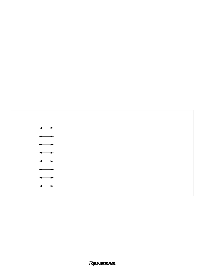
265
8.5
Port 4
8.5.1
Overview
Port 4 is an 8-bit input/output port also used for data bus, with the pin configuration shown in
figure 8.4. The pin functions differ depending on the operating mode.
In modes 1 to 5 (expanded modes), when the bus width control register (ABWCR) designates
areas 0 to 7 all as 8-bit-access areas, the chip operates in 8-bit bus mode and port 4 is a generic
input/output port. When at least one of areas 0 to 7 is designated as a 16-bit-access area, the chip
operates in 16-bit bus mode and port 4 becomes part of the data bus. In mode 7 (single-chip
mode), port 4 is a generic input/output port.
Port 4 has software-programmable built-in pull-up transistors.
Pins in port 4 can drive one TTL load and a 90-pF capacitive load. They can also drive a
darlington transistor pair.
Port 4
P4 /D
P4 /D
P4 /D
P4 /D
P4 /D
P4 /D
P4 /D
P4 /D
7
6
5
4
3
2
1
0
7
6
5
4
3
2
1
0
P4 (input/output)/D
7
(input/output)
P4 (input/output)/D
6
(input/output)
P4 (input/output)/D
5
(input/output)
P4 (input/output)/D
4
(input/output)
P4 (input/output)/D
3
(input/output)
P4 (input/output)/D
2
(input/output)
P4 (input/output)/D
1
(input/output)
P4 (input/output)/D
0
(input/output)
7
6
5
4
3
2
1
0
Port 4 pins
Modes 1 to 5
P4 (input/output)
P4 (input/output)
P4 (input/output)
P4 (input/output)
P4 (input/output)
P4 (input/output)
P4 (input/output)
P4 (input/output)
7
6
5
4
3
2
1
0
Mode 7
Figure 8.4 Port 4 Pin Configuration
266
8.5.2
Register Descriptions
Table 8.6 summarizes the registers of port 4.
Table 8.6
Port 4 Registers
Address
*
Name
Abbreviation
R/W
Initial Value
H'EE003
Port 4 data direction register
P4DDR
W
H'00
H'FFFD3
Port 4 data register
P4DR
R/W
H'00
H'EE03E
Port 4 input pull-up control register
P4PCR
R/W
H'00
Note:
*
Lower 20 bits of the address in advanced mode.
Port 4 Data Direction Register (P4DDR): P4DDR is an 8-bit write-only register that can select
input or output for each pin in port 4.
Bit
Initial value
Read/Write
7
P4 DDR
0
W
Port 4 data direction 7 to 0
These bits select input or output for port 4 pins
7
6
P4 DDR
0
W
6
5
P4 DDR
0
W
5
4
P4 DDR
0
W
4
3
P4 DDR
0
W
3
2
P4 DDR
0
W
2
1
P4 DDR
0
W
1
0
P4 DDR
0
W
0
Modes 1 to 5 (Expanded Modes): When all areas are designated as 8-bit-access areas by the bus
controller's bus width control register (ABWCR), selecting 8-bit bus mode, port 4 functions as an
input/output port. In this case, a pin in port 4 becomes an output port if the corresponding P4DDR
bit is set to 1, and an input port if this bit is cleared to 0.
When at least one area is designated as a 16-bit-access area, selecting 16-bit bus mode, port 4
functions as part of the data bus, regardless of the P4DDR settings.
Mode 7 (Single-Chip Mode): Port 4 functions as an input/output port. A pin in port 4 becomes an
output port if the corresponding P4DDR bit is set to 1, and an input port if this bit is cleared to 0.
P4DDR is a write-only register. Its value cannot be read. All bits return 1 when read.
P4DDR is initialized to H'00 by a reset and in hardware standby mode. In software standby mode
it retains its previous setting.
267
ABWCR and P4DDR are not initialized in software standby mode. Therefore, if a transition is
made to software standby mode while port 4 is functioning as an input/output port and a P4DDR
bit is set to 1, the corresponding pin maintains its output state.
Port 4 Data Register (P4DR): P4DR is an 8-bit readable/writable register that stores output data
for port 4. When port 4 functions as an output port, the value of this register is output. When a bit
in P4DDR is set to 1, if port 4 is read the value of the corresponding P4DR bit is returned. When a
bit in P4DDR is cleared to 0, if port 4 is read the corresponding pin logic level is read.
Bit
Initial value
Read/Write
7
P4
0
R/W
Port 4 data 7 to 0
These bits store data for port 4 pins
7
6
P4
0
R/W
6
5
P4
0
R/W
5
4
P4
0
R/W
4
3
P4
0
R/W
3
2
P4
0
R/W
2
1
P4
0
R/W
1
0
P4
0
R/W
0
P4DR is initialized to H'00 by a reset and in hardware standby mode. In software standby mode it
retains its previous setting.
Port 4 Input Pull-Up MOS Control Register (P4PCR): P4PCR is an 8-bit readable/writable
register that controls the MOS input pull-up transistors in port 4.
Bit
Initial value
Read/Write
7
P4 PCR
0
R/W
Port 4 input pull-up control 7 to 0
These bits control input pull-up transistors built into port 4
7
6
P4 PCR
0
R/W
6
5
P4 PCR
0
R/W
5
4
P4 PCR
0
R/W
4
3
P4 PCR
0
R/W
3
2
P4 PCR
0
R/W
2
1
P4 PCR
0
R/W
1
0
P4 PCR
0
R/W
0
In mode 7 (single-chip mode), and in 8-bit bus mode in modes 1 to 5 (expanded modes), when a
P4DDR bit is cleared to 0 (selecting generic input), if the corresponding P4PCR bit is set to 1, the
input pull-up transistor is turned on.
P4PCR is initialized to H'00 by a reset and in hardware standby mode. In software standby mode it
retains its previous setting.

268
Table 8.7 summarizes the states of the input pull-up transistors in each operating mode.
Table 8.7
Input Pull-Up Transistor States (Port 4)
Mode
Reset
Hardware
Standby Mode
Software
Standby Mode
Other Modes
1 to 5
8-bit bus mode
Off
Off
On/off
On/off
16-bit bus mode
Off
Off
7
On/off
On/off
Legend
Off:
The input pull-up transistor is always off.
On/off: The input pull-up transistor is on if P4PCR = 1 and P4DDR = 0. Otherwise, it is off.
269
8.6
Port 5
8.6.1
Overview
Port 5 is a 4-bit input/output port also used for address output, with the pin configuration shown in
figure 8.5. The pin functions differ depending on the operating mode.
In modes 1 to 4 (expanded modes with on-chip ROM disabled), port 5 consists of address output
pins (A
19
to A
16
). In mode 5 (expanded mode with on-chip ROM enabled), settings in the port 5
data direction register (P5DDR) designate pins for address bus output (A
19
to A
16
) or generic input.
In mode 7 (single-chip mode), port 5 is a generic input/output port.
Port 5 has software-programmable built-in pull-up transistors.
Pins in port 5 can drive one TTL load and a 90-pF capacitive load. They can also drive an LED or
a darlington transistor pair.
Port 5
P5 /A
P5 /A
P5 /A
P5 /A
3
2
1
0
19
18
17
16
A (output)
A (output)
A (output)
A (output)
19
18
17
16
P5 (input)/A (output)
P5 (input)/A (output)
P5 (input)/A (output)
P5 (input)/A (output)
3
2
1
0
Port 5
pins
Modes 1 to 4
Mode 5
P5 (input/output)
P5 (input/output)
P5 (input/output)
P5 (input/output)
3
2
1
0
Mode 7
19
18
17
16
Figure 8.5 Port 5 Pin Configuration
8.6.2
Register Descriptions
Table 8.8 summarizes the registers of port 5.
Table 8.8
Port 5 Registers
Initial Value
Address
*
Name
Abbreviation
R/W
Modes 1 to 4 Modes 5 and 7
H'EE004
Port 5 data direction register
P5DDR
W
H'FF
H'F0
H'FFFD4 Port 5 data register
P5DR
R/W
H'F0
H'F0
H'EE03F Port 5 input pull-up control register
P5PCR
R/W
H'F0
H'F0
Note:
*
Lower 20 bits of the address in advanced mode.

270
Port 5 Data Direction Register (P5DDR): P5DDR is an 8-bit write-only register that can select
input or output for each pin in port 5.
Bits 7 to 4 are reserved. They are fixed at 1, and cannot be modified.
Bit
Modes
1 to 4
Initial value
Read/Write
Initial value
Read/Write
Modes
5 and 7
7
--
1
--
1
--
6
--
1
--
1
--
5
--
1
--
1
--
4
--
1
--
1
--
3
P5 DDR
1
--
0
W
3
2
P5 DDR
1
--
0
W
2
1
P5 DDR
1
--
0
W
1
0
P5 DDR
1
--
0
W
0
Reserved bits
Port 5 data direction 3 to 0
These bits select input or
output for port 5 pins
Modes 1 to 4 (Expanded Modes with On-Chip ROM Disabled): P5DDR values are fixed at 1.
Port 5 functions as an address bus.
Mode 5 (Expanded Mode with On-Chip ROM Enabled): Following a reset, port 5 is an input
port. A pin in port 5 becomes an address output pin if the corresponding P5DDR bit is set to 1, and
an input port if this bit is cleared to 0.
Mode 7 (Single-Chip Mode): Port 5 functions as an input/output port. A pin in port 5 becomes an
output port if the corresponding P5DDR bit is set to 1, and an input port if this bit is cleared to 0.
In modes 1 to 4, P5DDR bits are always read as 1, and cannot be modified.
In modes 5 and 7, P5DDR is a write-only register. Its value cannot be read. All bits return 1 when
read.
P5DDR is initialized to H'FF in modes 1 to 4, and to H'F0 in modes 5 and 7, by a reset and in
hardware standby mode. In software standby mode it retains its previous setting. Therefore, if a
transition is made to software standby mode while port 5 is functioning as an input/output port and
a P5DDR bit is set to 1, the corresponding pin maintains its output state.
271
Port 5 Data Register (P5DR): P5DR is an 8-bit readable/writable register that stores output data
for port 5. When port 5 functions as an output port, the value of this register is output. When a bit
in P5DDR is set to 1, if port 5 is read the value of the corresponding P5DR bit is returned. When a
bit in P5DDR is cleared to 0, if port 5 is read the corresponding pin logic level is read.
Bits 7 to 4 are reserved. They are fixed at 1, and cannot be modified.
Bit
Initial value
Read/Write
7
--
1
--
6
--
1
--
5
--
1
--
4
--
1
--
3
P5
0
R/W
3
2
P5
0
R/W
2
1
P5
0
R/W
1
0
P5
0
R/W
0
Reserved bits
These bits store data
for port 5 pins
Port 5 data 3 to 0
P5DR is initialized to H'F0 by a reset and in hardware standby mode. In software standby mode it
retains its previous setting.
Port 5 Input Pull-Up MOS Control Register (P5PCR): P5PCR is an 8-bit readable/writable
register that controls the MOS input pull-up transistors in port 5.
Bits 7 to 4 are reserved. They are fixed at 1, and cannot be modified.
Bit
Initial value
Read/Write
7
--
1
--
6
--
1
--
5
--
1
--
4
--
1
--
3
P5 PCR
0
R/W
3
2
P5 PCR
0
R/W
2
1
P5 PCR
0
R/W
1
0
P5 PCR
0
R/W
0
Reserved bits
These bits control input pull-up
transistors built into port 5
Port 5 input pull-up control 3 to 0
In modes 5 and 7, when a P5DDR bit is cleared to 0 (selecting generic input), if the corresponding
bit in P5PCR is set to 1, the input pull-up transistor is turned on.
P5PCR is initialized to H'F0 by a reset and in hardware standby mode. In software standby mode
it retains its previous setting.
Table 8.9 summarizes the states of the input pull-ups in each mode.

272
Table 8.9
Input Pull-Up Transistor States (Port 5)
Mode
Reset
Hardware Standby Mode
Software Standby Mode
Other Modes
1
2
3
4
Off
Off
Off
Off
5
7
Off
Off
On/off
On/off
Legend
Off:
The input pull-up transistor is always off.
On/off: The input pull-up transistor is on if P5PCR = 1 and P5DDR = 0. Otherwise, it is off.

273
8.7
Port 6
8.7.1
Overview
Port 6 is an 8-bit input/output port that is also used for input and output of bus control signals
(
LWR, HWR, RD, AS, BACK, BREQ, WAIT) and for clock (
) output.
The pin configuration of port 6 is shown in figure 8.6.
In modes 1 to 5 (expanded modes), the pin functions are P6
7
(generic input)/
,
LWR, HWR, RD,
AS, P6
2
/
BACK, P6
1
/
BREQ, and P6
0
/
WAIT). See table 8.11 for the selection of the pin functions.
In mode 7 (single-chip mode), P6
7
functions as a generic input port or � output, and P6
6
to P6
0
function as generic input/output ports.
When DRAM is connected to areas 2 to 5,
LWR, HWR, and RD also function as LCAS, UCAS,
and
WE, respectively. For details see section 6.5, DRAM Interface.
Pins in port 6 can drive one TTL load and a 90-pF capacitive load. They can also drive a
darlington transistor pair.
Port 6
P6 /
P6 /
P6 /
P6 /
P6 /
P6 /
P6 /
P6 /
7
6
5
4
3
2
1
0
LWR
HWR
RD
AS
BACK
BREQ
WAIT
Port 6 pins
LWR
HWR
RD
AS
BACK
BREQ
WAIT
Modes 1 to 5
(expanded modes)
(output)
(output)
(output)
(output)
(output)
(output)
(input)
(input)
P6
P6
P6
P6
P6
P6
P6
P6
7
6
5
4
3
2
1
0
Mode 7
(single-chip mode)
(input) /
(output)
(input/output)
(input/output)
(input/output)
(input/output)
(input/output)
(input/output)
(input/output)
P6
7
(input)/
P6
2
(input/output)/
P6
1
(input/output)/
P6
0
(input/output)/
Figure 8.6 Port 6 Pin Configuration

274
8.7.2
Register Descriptions
Table 8.10 summarizes the registers of port 6.
Table 8.10
Port 6 Registers
Address
*
Name
Abbreviation
R/W
Initial Value
H'EE005
Port 6 data direction register
P6DDR
W
H'80
H'FFFD5
Port 6 data register
P6DR
R/W
H'80
Note:
*
Lower 20 bits of the address in advanced mode.
Port 6 Data Direction Register (P6DDR): P6DDR is an 8-bit write-only register that can select
input or output for each pin in port 6.
Bit 7 is reserved. It is fixed at 1, and cannot be modified.
Bit
Initial value
Read/Write
7
--
1
--
6
P6 DDR
0
W
6
5
P6 DDR
0
W
5
4
P6 DDR
0
W
4
3
P6 DDR
0
W
3
2
P6 DDR
0
W
2
1
P6 DDR
0
W
1
0
P6 DDR
0
W
0
Port 6 data direction 6 to 0
These bits select input or output for port 6 pins
Reserved bit
Modes 1 to 5 (Expanded Modes): P6
7
functions as the clock output pin (
) or an input port. P6
7
is the clock output pin (�) if the PSTOP bit in MSTRCH is cleared to 0 (initial value), and an input
port if this bit is set to 1.
P6
6
to P6
3
function as bus control output pins (
LWR, HWR, RD, and AS), regardless of the
settings of bits P6
6
DDR to P6
3
DDR.
P6
2
to P6
0
function as bus control input/output pins (
BACK, BREQ, and WAIT) or input/output
ports. For the method of selecting the pin functions, see table 8.11.
When P6
2
to P6
0
function as input/output ports, the pin becomes an output port if the
corresponding P6DDR bit is set to 1, and an input port if this bit is cleared to 0.
Mode 7 (Single-Chip Mode): P6
7
functions as the clock output pin (
) or an input port. P6
6
to
P6
0
function as generic input/output ports. P6
7
is the clock output pin (
) if the PSTOP bit in
MSTCRH is cleared to 0, and an input port if this bit is set to 1 (initial value). A pin in port 6
becomes an output port if the corresponding bit of P6
6
DDR to P6
0
DDR is set to 1, and an input
port if this pin is cleared to 0.

275
P6DDR is a write-only register. Its value cannot be read. All bits return 1 when read.
P6DDR is initialized to H'80 by a reset and in hardware standby mode. In software standby mode
it retains its previous setting. Therefore, if a transition is made to software standby mode while
port 6 is functioning as an input/output port and a P6DDR bit is set to 1, the corresponding pin
maintains its output state.
Port 6 Data Register (P6DR): P6DR is an 8-bit readable/writable register that stores output data
for port 6. When port 6 functions as an output port, the value of this register is output. For bit 7, a
value of 1 is returned if the bit is read while the PSTOP bit in MSTCRH is cleared to 0, and the
P67 pin logic level is returned if the bit is read while the PSTOP bit is set to 1. Bit 7 cannot be
modified. For bits 6 to 0, the pin logic level is returned if the bit is read while the corresponding
bit in P6DDR is cleared to 0, and the P6DR value is returned if the bit is read while the
corresponding bit in P6DDR is set to 1.
Bit
Initial value
Read/Write
7
P6
7
1
R
6
P6
0
R/W
6
5
P6
0
R/W
5
4
P6
0
R/W
4
3
P6
0
R/W
3
2
P6
0
R/W
2
1
P6
0
R/W
1
0
P6
0
R/W
0
Port 6 data 7 to 0
These bits store data for port 6 pins
P6DR is initialized to H'80 by a reset and in hardware standby mode. In software standby mode it
retains its previous setting.
276
Table 8.11
Port 6 Pin Functions in Modes 1 to 5
Pin
Pin Functions and Selection Method
P6
7
/
Bit PSTOP in MSTCRH selects the pin function.
PSTOP
0
1
Pin function
output
P6
7
input
LWR
Functions as
LWR
regardless of the setting of bit P6
6
DDR.
P6
6
DDR
0
1
Pin function
LWR
output
*
Note:
*
If any of bits DRAS2 to DRAS0 in DRCRA is 1 and bit CSEL in DRCRB is 1,
LWR
output functions as
LCAS
.
HWR
Functions as
HWR
regardless of the setting of bit P6
5
DDR.
P6
5
DDR
0
1
Pin function
HWR
output
*
Note:
*
If any of bits DRAS2 to DRAS0 in DRCRA is 1 and bit CSEL in DRCRB is 1,
HWR
output functions as
UCAS
.
RD
Functions as
RD
regardless of the setting of bit P6
4
DDR.
P6
4
DDR
0
1
Pin function
RD
output
*
Note:
*
If any of bits DRAS2 to DRAS0 in DRCRA is 1,
RD
output functions as
WE
.
AS
Functions as
AS
regardless of the setting of bit P6
3
DDR.
P6
3
DDR
0
1
Pin function
AS
output
P6
2
/
BACK
Bit BRLE in BRCR and bit P6
2
DDR select the pin function as follows.
BRLE
0
1
P6
2
DDR
0
1
--
Pin function
P6
2
input
P6
2
output
BACK
output
P6
1
/
BREQ
Bit BRLE in BRCR and bit P6
1
DDR select the pin function as follows.
BRLE
0
1
P6
1
DDR
0
1
--
Pin function
P6
1
input
P6
1
output
BREQ
input
P6
0
/
WAIT
Bit WAITE in BCR and bit P6
0
DDR select the pin function as follows.
WAITE
0
1
P6
0
DDR
0
1
0
*
Pin function
P6
0
input
P6
0
output
WAIT
input
Note:
*
Do not set bit P6
0
DDR to 1.
277
8.8
Port 7
8.8.1
Overview
Port 7 is an 8-bit input port that is also used for analog input to the A/D converter and analog
output from the D/A converter. The pin functions are the same in all operating modes. Figure 8.7
shows the pin configuration of port 7.
See section 15, A/D Converter, for details of the A/D converter analog input pins, and section 16,
D/A Converter, for details of the D/A converter analog output pins.
Port 7
P7 (input)/AN (input)/DA (output)
P7 (input)/AN (input)/DA (output)
P7 (input)/AN (input)
P7 (input)/AN (input)
P7 (input)/AN (input)
P7 (input)/AN (input)
P7 (input)/AN (input)
P7 (input)/AN (input)
7
6
5
4
3
2
1
0
7
6
5
4
3
2
1
0
Port 7 pins
1
0
Figure 8.7 Port 7 Pin Configuration

278
8.8.2
Register Description
Table 8.12 summarizes the port 7 register. Port 7 is an input port, and port 7 has no data direction
register.
Table 8.12
Port 7 Data Register
Address
*
Name
Abbreviation
R/W
Initial Value
H'FFFD6
Port 7 data register
P7DR
R
Undetermined
Note:
*
Lower 20 bits of the address in advanced mode.
Port 7 Data Register (P7DR)
Bit
Initial value
Read/Write
0
P7
--
R
*
Note:
*
0
1
P7
--
R
*
1
2
P7
--
R
*
2
3
P7
--
*
R
3
4
P7
--
R
*
4
5
P7
--
R
*
5
6
P7
--
R
*
6
7
P7
--
R
*
7
7
0
Determined by pins P7 to P7 .
When port 7 is read, the pin logic levels are always read. P7DR cannot be modified.

279
8.9
Port 8
8.9.1
Overview
Port 8 is a 5-bit input/output port that is also used for
CS
3
to
CS
0
output,
RFSH output, IRQ
3
to
IRQ
0
input, and A/D converter
ADTRG input. Figure 8.8 shows the pin configuration of port 8.
In modes 1 to 5 (expanded modes), port 8 can provide
CS
3
to
CS
0
output,
RFSH output, IRQ
3
to
IRQ
0
input, and
ADTRG input. See table 8.14 for the selection of pin functions in expanded
modes.
In mode 7 (single-chip mode), port 8 can provide
IRQ
3
to
IRQ
0
input and
ADTRG input. See table
8.15 for the selection of pin functions in single-chip mode.
See section 15, A/D Converter, for a description of the A/D converter's
ADTRG input pin.
The
IRQ
3
to
IRQ
0
functions are selected by IER settings, regardless of whether the pin is used for
input or output. Caution is therefore required. For details see section 5.3.1, External Interrupts.
When DRAM is connected to areas 2 to 5, the
CS
3
and
CS
2
output pins function as
RAS output
pins for each area. For details see section 6.5, DRAM Interface.
Pins in port 8 can drive one TTL load and a 90-pF capacitive load. They can also drive a
darlington transistor pair.
Pins P8
2
to P8
0
have Schmitt-trigger inputs.
280
Port 8
P8 /
P8 / /
P8 / /
P8 / /
P8 / /
4
3
2
1
0
0
1
2
3
Port 8 pins
CS
CS
CS
CS
RFSH
3
2
1
IRQ / ADTRG
IRQ
IRQ
IRQ
0
P8 (input)/ (output)
P8 (input)/ (output)/ (input) / ADTRG (input)
P8 (input)/ (output)/ (input)
P8 (input/output)/ CS
3
(output)/IRQ
1
(input)
P8 (input/output)/ (output)/ (input)
4
3
2
1
0
Pin functions in modes 1 to 5
(expanded modes)
0
1
2
CS
CS
CS
RFSH
3
2
IRQ
IRQ
IRQ
0
P8 /(input/output)
P8 /(input/output)/ (input) /
P8 /(input/output)/ (input)
P8 /(input/output)/ (input)
P8 /(input/output)/ (input)
4
3
2
1
0
Pin functions in mode 7
(single-chip mode)
IRQ
IRQ
IRQ
IRQ
ADTRG (input)
3
2
1
0
Figure 8.8 Port 8 Pin Configuration
281
8.9.2
Register Descriptions
Table 8.13 summarizes the registers of port 8.
Table 8.13
Port 8 Registers
Initial Value
Address
*
Name
Abbreviation
R/W
Modes 1 to 4
Modes 5 and 7
H'EE007
Port 8 data direction
register
P8DDR
W
H'F0
H'E0
H'FFFD7
Port 8 data register
P8DR
R/W
H'E0
H'E0
Note:
*
Lower 20 bits of the address in advanced mode.
Port 8 Data Direction Register (P8DDR): P8DDR is an 8-bit write-only register that can select
input or output for each pin in port 8.
Bits 7 to 5 are reserved. They are fixed at 1, and cannot be modified.
7
--
1
--
1
--
6
--
1
--
1
--
5
--
1
--
1
--
4
P8 DDR
1
W
0
W
4
3
P8 DDR
0
W
0
W
3
2
P8 DDR
0
W
0
W
2
1
P8 DDR
0
W
0
W
1
0
P8 DDR
0
W
0
W
0
Reserved bits
Port 8 data direction 4 to 0
These bits select input or
output for port 8 pins
Bit
Modes
1 to 4
Initial value
Read/Write
Initial value
Read/Write
Modes
5 and 7
Modes 1 to 5 (Expanded Modes): When bits in P8DDR bit are set to 1, P8
4
to P8
1
become
CS
0
to
CS
3
output pins. When bits in P8DDR are cleared to 0, the corresponding pins become input ports.
However, P8
1
can also be used as an output port, depending on the setting of bits DRAS2 to
DRAS0 in DRAM control register A (DRCRA). For details see section 6.5.2, DRAM Space and
RAS Output Pin Settings.
In modes 1 to 4 (expanded modes with on-chip ROM disabled), following a reset P8
4
functions as
the
CS
0
output, while
CS
1
to
CS
3
are input ports. In mode 5 (expanded mode with on-chip ROM
enabled), following a reset
CS
0
to
CS
3
are all input ports.
When the refresh enable bit (RFSHE) in DRCRA is set to 1, P8
0
is used for
RFSH output. When
RFSHE is cleared to 0, P8
0
becomes an input/output port according to the P8DDR setting. For
details see table 8.14.

282
Mode 7 (Single-Chip Mode): Port 8 is a generic input/output port. A pin in port 8 becomes an
output port if the corresponding P8DDR bit is set to 1, and an input port if this bit is cleared to 0.
P8DDR is a write-only register. Its value cannot be read. All bits return 1 when read.
P8DDR is initialized to H'F0 in modes 1 to 4, and to H'E0 in modes 5 and 7, by a reset and in
hardware standby mode. In software standby mode P8DDR retains its previous setting. Therefore,
if a transition is made to software standby mode while port 8 is functioning as an input/output port
and a P8DDR bit is set to 1, the corresponding pin maintains its output state.
Port 8 Data Register (P8DR): P8DR is an 8-bit readable/writable register that stores output data
for port 8. When port 8 functions as an output port, the value of this register is output. When a bit
in P8DDR is set to 1, if port 8 is read the value of the corresponding P8DR bit is returned. When a
bit in P8DDR is cleared to 0, if port 8 is read the corresponding pin logic level is read.
Bits 7 to 5 are reserved. They are fixed at 1, and cannot be modified.
Bit
Initial value
Read/Write
7
--
1
--
6
--
1
--
5
--
1
--
4
P8
0
R/W
4
3
P8
0
R/W
3
2
P8
0
R/W
2
1
P8
0
R/W
1
0
P8
0
R/W
0
Reserved bits
Port 8 data 4 to 0
These bits store data
for port 8 pins
P8DR is initialized to H'E0 by a reset and in hardware standby mode. In software standby mode it
retains its previous setting.
283
Table 8.14
Port 8 Pin Functions in Modes 1 to 5
Pin
Pin Functions and Selection Method
P8
4
/
CS
0
Bit P8
4
DDR selects the pin function as follows.
P8
4
DDR
0
1
Pin function
P8
4
input
CS
0
output
P8
3
/
CS
1
/
IRQ
3
/
ADTRG
Bit P8
3
DDR selects the pin function as follows.
P8
3
DDR
0
1
Pin function
P8
3
input
CS
1
output
IRQ
3
input
ADTRG
input
P8
2
/
CS
2
/
IRQ
2
The DRAM interface settings by bits DRAS2 to DRAS0 in DRCRA, and bit P8
2
DDR, select the
pin function as follows.
DRAM interface
settings
(1) in table below
|(2) in table below
P8
2
DDR
0
1
--
Pin function
P8
2
input
CS
2
output
CS
2
output
*
IRQ
3
input
Note:
*
CS
2
is output as
RAS
2
.
DRAM interface
setting
(1)
(2)
DRAS2
0
1
DRAS1
0
1
0
1
DRAS0
0
1
0
1
0
1
0
1
P8
1
/
CS
3
/
IRQ
1
The DRAM interface settings by bits DRAS2 to DRAS0 in DRCRA, and bit P8
1
DDR, select the
pin function as follows.
DRAM interface
settings
(1) in table below
(2) in table below
(3) in table below
P8
1
DDR
0
1
0
1
--
Pin function
P8
1
input
pin
CS
3
output
pin
P8
1
input
pin
P8
1
output
pin
CS
3
output pin
*
IRQ
1
input pin
Note:
*
CS
3
is output as
RAS
3
.
DRAM interface
setting
(1)
(3)
(2)
(3)
(2)
DRAS2
0
1
DRAS1
0
1
0
1
DRAS0
0
1
0
1
0
1
0
1
P8
0
/
RFSH
/
IRQ
0
Bit RFSHE in DRCRA and bit P8
0
DDR select the pin function as follows.
RFSHE
0
1
*
P8
0
DDR
0
1
--
Pin function
P8
0
input
P8
0
output
RFSH
output
IRQ
0
input
Note:
*
If areas 2 to 5 are not designated as DRAM space, this bit should not be set to 1.
284
Table 8.15
Port 8 Pin Functions in Mode 7
Pin
Pin Functions and Selection Method
P8
4
Bit P8
4
DDR selects the pin function as follows.
P8
4
DDR
0
1
Pin function
P8
4
input
P8
4
output
P8
3
/
IRQ
3
/
ADTRG
Bit P8
3
DDR selects the pin function as follows.
P8
3
DDR
0
1
Pin function
P8
3
input
P8
3
output
IRQ
3
input
ADTRG
input
P8
2
/
IRQ
2
Bit P8
2
DDR selects the pin function as follows.
P8
2
DDR
0
1
Pin function
P8
2
input
P8
2
output
IRQ
2
input
P8
1
/
IRQ
1
Bit P8
1
DDR selects the pin function as follows.
P8
1
DDR
0
1
Pin function
P8
1
input
P8
1
output
IRQ
1
input
P8
0
/
IRQ
0
Bit P8
0
DDR select the pin function as follows.
P8
0
DDR
0
1
Pin function
P8
0
input
P8
0
output
IRQ
0
input
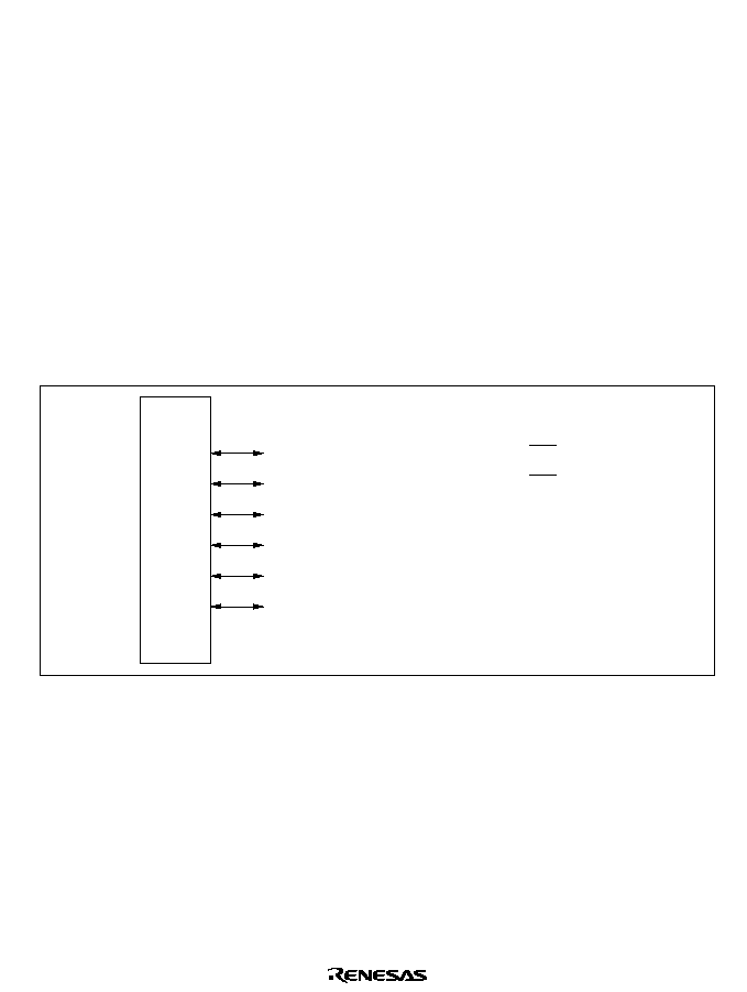
285
8.10
Port 9
8.10.1
Overview
Port 9 is a 6-bit input/output port that is also used for input and output (TxD
0
, TxD
1
, RxD
0
, RxD
1
,
SCK
0
, SCK
1
) by serial communication interface channels 0 and 1 (SCI0 and SCI1), and for
IRQ
5
and
IRQ
4
input. See table 8.17 for the selection of pin functions.
The
IRQ
5
and
IRQ
4
functions are selected by IER settings, regardless of whether the pin is used
for input or output. Caution is therefore required. For details see section 5.3.1, External Interrupts.
Port 9 has the same set of pin functions in all operating modes. Figure 8.9 shows the pin
configuration of port 9.
Pins in port 9 can drive one TTL load and a 30-pF capacitive load. They can also drive a
darlington transistor pair.
Port 9
P9 (input/output)/SCK
P9 (input/output)/SCK
P9 (input/output)/RxD (input)
P9 (input/output)/RxD (input)
P9 (input/output)/TxD (output)
P9 (input/output)/TxD (output)
5
4
3
2
1
0
Port 9 pins
1
0
(input/output)/IRQ (input)
(input/output)/IRQ (input)
5
4
1
0
1
0
Figure 8.9 Port 9 Pin Configuration

286
8.10.2
Register Descriptions
Table 8.16 summarizes the registers of port 9.
Table 8.16
Port 9 Registers
Address
*
Name
Abbreviation
R/W
Initial Value
H'EE008
Port 9 data direction register
P9DDR
W
H'C0
H'FFFD8
Port 9 data register
P9DR
R/W
H'C0
Note:
*
Lower 20 bits of the address in advanced mode.
Port 9 Data Direction Register (P9DDR): P9DDR is an 8-bit write-only register that can select
input or output for each pin in port 9.
Bits 7 and 6 are reserved. They are fixed at 1, and cannot be modified.
Bit
Initial value
Read/Write
7
--
1
--
6
--
1
--
5
P9 DDR
0
W
5
4
P9 DDR
0
W
4
3
P9 DDR
0
W
3
2
P9 DDR
0
W
2
1
P9 DDR
0
W
1
0
P9 DDR
0
W
0
Reserved bits
Port 9 data direction 5 to 0
These bits select input or
output for port 9 pins
When port 9 functions as an input/output port, a pin in port 9 becomes an output port if the
corresponding P9DDR bit is set to 1, and an input port if this bit is cleared to 0. For the method of
selecting the pin functions, see table 8.17.
P9DDR is a write-only register. Its value cannot be read. All bits return 1 when read.
P9DDR is initialized to H'C0 by a reset and in hardware standby mode. In software standby mode
it retains its previous setting. Therefore, if a transition is made to software standby mode while
port 9 is functioning as an input/output port and a P9DDR bit is set to 1, the corresponding pin
maintains its output state.

287
Port 9 Data Register (P9DR): P9DR is an 8-bit readable/writable register that stores output data
for port 9. When port 9 functions as an output port, the value of this register is output. When a bit
in P9DDR is set to 1, if port 9 is read the value of the corresponding P9DR bit is returned. When a
bit in P9DDR is cleared to 0, if port 9 is read the corresponding pin logic level is read.
Bits 7 and 6 are reserved. They are fixed at 1, and cannot be modified.
Bit
Initial value
Read/Write
7
--
1
--
6
--
1
--
5
P9
0
R/W
4
P9
0
R/W
4
3
P9
0
R/W
3
2
P9
0
R/W
2
1
P9
0
R/W
1
0
P9
0
R/W
0
Reserved bits
Port 9 data 5 to 0
These bits store data
for port 9 pins
5
P9DR is initialized to H'C0 by a reset and in hardware standby mode. In software standby mode it
retains its previous setting.
288
Table 8.17
Port 9 Pin Functions
Pin
Pin Functions and Selection Method
P9
5
/SCK
1
/
IRQ
5
Bit C/
A
in SMR of SCI1, bits CKE0 and CKE1 in SCR, and bit P9
5
DDR select the pin function
as follows.
CKE1
0
1
C/
A
0
1
--
CKE0
0
1
--
--
P9
5
DDR
0
1
--
--
--
Pin function
P9
5
input
P9
5
output
SCK
1
output
SCK
1
output
SCK
1
input
IRQ
5
input
P9
4
/SCK
0
/
IRQ
4
Bit C/
A
in SMR of SCI0, bits CKE0 and CKE1 in SCR, and bit P9
4
DDR select the pin function
as follows.
CKE1
0
1
C/
A
0
1
--
CKE0
0
1
--
--
P9
4
DDR
0
1
--
--
--
Pin function
P9
4
input
P9
4
output
SCK
0
output
SCK
0
output
SCK
0
input
IRQ
4
input
P9
3
/RxD
1
Bit RE in SCR of SCI1, bit SMIF in SCMR, and bit P9
3
DDR select the pin function as follows.
SMIF
0
1
RE
0
1
--
P9
3
DDR
0
--
--
Pin function
P9
3
input
P9
3
output
RxD
1
input
RxD
1
input
P9
2
/RxD
0
Bit RE in SCR of SCI0, bit SMIF in SCMR, and bit P9
2
DDR select the pin function as follows.
SMIF
0
1
RE
0
1
--
P9
2
DDR
0
1
--
--
Pin function
P9
2
input
P9
2
output
RxD
0
input
RxD
0
input
289
Pin
Pin Functions and Selection Method
P9
1
/TxD
1
Bit TE in SCR of SCI1, bit SMIF in SCMR, and bit P9
1
DDR select the pin function as follows.
SMIF
0
1
TE
0
1
--
P9
1
DDR
0
1
--
--
Pin function
P9
1
input
P9
1
output
TxD
1
output
TxD
1
output
*
Note:
*
Functions as the TxD
1
output pin, but there are two states: one in which the pin is
driven, and another in which the pin is at high-impedance.
P9
0
/TxD
0
Bit TE in SCR of SCI0, bit SMIF in SCMR, and bit P9
0
DDR select the pin function as follows.
SMIF
0
1
TE
0
1
--
P9
0
DDR
0
1
--
--
Pin function
P9
0
input
P9
0
output
TxD
0
output
TxD
0
output
*
Note:
*
Functions as the TxD
0
output pin, but there are two states: one in which the pin is
driven, and another in which the pin is at high-impedance.

290
8.11
Port A
8.11.1
Overview
Port A is an 8-bit input/output port that is also used for output (TP
7
to TP
0
) from the programmable
timing pattern controller (TPC), input and output, (TIOCB
2
, TIOCA
2
, TIOCB
1
, TIOCA
1
, TIOCB
0
,
TIOCA
0
, TCLKD, TCLKC, TCLKB, TCLKA) by the 16-bit timer, input (TCLKD, TCLKC,
TCLKB, TCLKA) to the 8-bit timer, output (
TEND
1
,
TEND
0
) from the DMA controller (DMAC),
and address output (A
23
to A
20
). A reset or hardware standby transition leaves port A as an input
port, except that in modes 3 and 4, one pin is always used for A
20
output. See table 8.19 to 8.21 for
the selection of pin functions.
Usage of pins for TPC, 16-bit timer, 8-bit timer, and DMAC input and output is described in the
sections on those modules. For output of address bits A
23
to A
20
in modes 3, 4, and 5, see section
6.2.4, Bus Release Control Register (BRCR). Pins not assigned to any of these functions are
available for generic input/output. Figure 8.10 shows the pin configuration of port A.
Pins in port A can drive one TTL load and a 30-pF capacitive load. They can also drive a
darlington transistor pair. Port A has Schmitt-trigger inputs.
291
Port A
PA /TP /TIOCB /A
PA /TP /TIOCA /A
21
PA /TP /TIOCB /A
22
PA /TP /TIOCA /A
23
PA /TP /TIOCB /TCLKD
PA /TP /TIOCA /TCLKC
PA /TP /
TEND
/TCLKB
PA /TP /
TEND
/TCLKA
7
6
5
4
3
2
1
0
Port A pins
7
6
5
4
3
2
1
0
2
2
1
1
1
0
0
0
PA (input/output)/TP (output)/TIOCB (input/output)
PA (input/output)/TP (output)/TIOCA (input/output)
PA (input/output)/TP (output)/TIOCB (input/output)
PA (input/output)/TP (output)/TIOCA (input/output)
7
6
5
4
3
2
1
0
Pin functions in modes 1, 2, and 7
PA (input/output)/TP (output)/TIOCB (input/output)/TCLKD (input)
PA (input/output)/TP (output)/TIOCA (input/output)/TCLKC (input)
PA (input/output)/TP (output)/
TEND
(output)/TCLKB (input)
PA (input/output)/TP (output)/
TEND
(output)/TCLKA (input)
Pin functions in mode 5
7
6
5
4
3
2
1
0
2
2
1
1
0
0
1
0
A (output)
20
PA (input/output)/TP (output)/TIOCA (input/output)/A (output)
PA (input/output)/TP (output)/TIOCB (input/output)/A (output)
PA (input/output)/TP (output)/TIOCA (input/output)/A (output)
6
5
4
3
2
1
0
Pin functions in modes 3 and 4
6
5
4
3
2
1
0
2
1
1
0
0
PA (input/output)/TP (output)/
TEND
(output)/TCLKA (input)
PA (input/output)/TP (output)/TIOCB (input/output)/TCLKD (input)
PA (input/output)/TP (output)/TIOCA (input/output)/TCLKC (input)
PA (input/output)/TP (output)/
TEND
(output)/TCLKB (input)
PA
7
(input/output)/TP
7
(output)/TIOCB
2
(input/output)/A (output)
PA
6
(input/output)/TP
6
(output)/TIOCA
2
(input/output)/A (output)
PA
5
(input/output)/TP
5
(output)/TIOCB
1
(input/output)/A (output)
PA
4
(input/output)/TP
4
(output)/TIOCA
1
(input/output)/A (output)
PA
3
(input/output)/TP
3
(output)/TIOCB
0
(input/output)/TCLKD (input)
PA
2
(input/output)/TP
2
(output)/TIOCA
0
(input/output)/TCLKC (input)
PA
1
(input/output)/TP
1
(output)/
TEND
1
(output)/TCLKB (input)
PA
0
(input/output)/TP
0
(output)/
TEND
0
(output)/TCLKA (input)
1
0
20
21
22
23
20
21
22
23
Figure 8.10 Port A Pin Configuration
292
8.11.2
Register Descriptions
Table 8.18 summarizes the registers of port A.
Table 8.18
Port A Registers
Initial Value
Address
*
Name
Abbreviati
on
R/W
Modes 1, 2, 5, and 7
Modes 3, 4
H'EE009
Port A data direction
register
PADDR
W
H'00
H'80
H'FFFD9
Port A data register
PADR
R/W
H'00
H'00
Note:
*
Lower 20 bits of the address in advanced mode.
Port A Data Direction Register (PADDR): PADDR is an 8-bit write-only register that can select
input or output for each pin in port A. When pins are used for TPC output, the corresponding
PADDR bits must also be set.
7
PA DDR
1
--
0
W
Port A data direction 7 to 0
These bits select input or output for port A pins
7
6
PA DDR
0
W
0
W
6
5
PA DDR
0
W
0
W
5
4
PA DDR
0
W
0
W
4
3
PA DDR
0
W
0
W
3
2
PA DDR
0
W
0
W
2
1
PA DDR
0
W
0
W
1
0
PA DDR
0
W
0
W
0
Bit
Modes
3, 4
Initial value
Read/Write
Initial value
Read/Write
Modes
1, 2, 5,
and 7
The pin functions that can be selected for pins PA
7
to PA
4
differ between modes 1, 2, and 7, and
modes 3 to 5. For the method of selecting the pin functions, see tables 8.19 and 8.20.
The pin functions that can be selected for pins PA
3
to PA
0
are the same in modes 1 to 5, 7. For the
method of selecting the pin functions, see table 8.21.
When port A functions as an input/output port, a pin in port A becomes an output port if the
corresponding PADDR bit is set to 1, and an input port if this bit is cleared to 0. In modes 3 and 4,
PA
7
DDR is fixed at 1 and PA
7
functions as the A
20
address output pin.
PADDR is a write-only register. Its value cannot be read. All bits return 1 when read.
PADDR is initialized to H'00 by a reset and in hardware standby mode in modes 1, 2, 5, and 7.
It is initialized to H'80 by a reset and in hardware standby mode in modes 3 and 4. In software
293
standby mode it retains its previous setting. Therefore, if a transition is made to software standby
mode while port A is functioning as an input/output port and a PADDR bit is set to 1, the
corresponding pin maintains its output state.
Port A Data Register (PADR): PADR is an 8-bit readable/writable register that stores output
data for port A. When port A functions as an output port, the value of this register is output. When
a bit in PADDR is set to 1, if port A is read the value of the corresponding PADR bit is returned.
When a bit in PADDR is cleared to 0, if port A is read the corresponding pin logic level is read.
Bit
Initial value
Read/Write
0
PA
0
R/W
0
1
PA
0
R/W
1
2
PA
0
R/W
2
3
PA
0
R/W
3
4
PA
0
R/W
4
5
PA
0
R/W
5
6
PA
0
R/W
6
7
PA
0
R/W
7
Port A data 7 to 0
These bits store data for port A pins
PADR is initialized to H'00 by a reset and in hardware standby mode. In software standby mode it
retains its previous setting.
Table 8.19
Port A Pin Functions (Modes 1, 2, 7)
Pin
Pin Functions and Selection Method
PA
7
/TP
7
/
TIOCB
2
Bit PWM2 in TMDR, bits IOB2 to IOB0 in TIOR2, bit NDER7 in NDERA, and bit PA
7
DDR select the pin
function as follows.
16-bit timer channel 2
settings
(1) in table below
(2) in table below
PA
7
DDR
--
0
1
1
NDER7
--
--
0
1
Pin function
TIOCB
2
output
PA
7
input
PA
7
output
TP
7
output
TIOCB
2
input
*
Note:
*
TIOCB
2
input when IOB2 = 1 and PWM2 = 0.
16-bit timer channel 2
settings
(2)
(1)
(2)
IOB2
0
1
IOB1
0
0
1
--
IOB0
0
1
--
--
294
Pin
Pin Functions and Selection Method
PA
6
/TP
6
/
TIOCA
2
Bit PWM2 in TMDR, bits IOA2 to IOA0 in TIOR2, bit NDER6 in NDERA, and bit PA
6
DDR select the pin
function as follows.
16-bit timer channel 2
settings
(1) in table below
(2) in table below
PA
6
DDR
--
0
1
1
NDER6
--
--
0
1
Pin function
TIOCA
2
output
PA
6
input
PA
6
output
TP
6
output
TIOCA
2
input
*
Note:
*
TIOCA
2
input when IOA2 = 1.
16-bit timer channel 2
settings
(2)
(1)
(2)
(1)
PWM2
0
1
IOA2
0
1
--
IOA1
0
0
1
--
--
IOA0
0
1
--
--
--
PA
5
/TP
5
/
TIOCB
1
Bit PWM1 in TMDR, bits IOB2 to IOB0 in TIOR1, bit NDER5 in NDERA, and bit PA
5
DDR select the pin
function as follows.
16-bit timer channel 1
settings
(1) in table below
(2) in table below
PA
5
DDR
--
0
1
1
NDER5
--
--
0
1
Pin function
TIOCB
1
output
PA
5
input
PA
5
output
TP
5
output
TIOCB
1
input
*
Note:
*
TIOCB
1
input when IOB2 = 1 and PWM1 = 0.
16-bit timer channel 1
settings
(2)
(1)
(2)
IOB2
0
1
IOB1
0
0
1
--
IOB0
0
1
--
--
295
Pin
Pin Functions and Selection Method
PA
4
/TP
4
/
TIOCA
1
Bit PWM1 in TMDR, bits IOA2 to IOA0 in TIOR1, bit NDER4 in NDERA, and bit PA
4
DDR select the pin
function as follows.
16-bit timer channel 1
settings
(1) in table below
(2) in table below
PA
4
DDR
--
0
1
1
NDER4
--
--
0
1
Pin function
TIOCA
1
output
PA
4
input
PA
4
output
TP
4
output
TIOCA
1
input
*
Note:
*
TIOCA
1
input when IOA2 = 1.
16-bit timer channel 1
settings
(2)
(1)
(2)
(1)
PWM1
0
1
IOA2
0
1
--
IOA1
0
0
1
--
--
IOA0
0
1
--
--
--
296
Table 8.20
Port A Pin Functions (Modes 3 to 5)
Pin
Pin Functions and Selection Method
PA
7
/TP
7
/
Modes 3 and 4: Always used as A
20
output.
TIOCB
2
/ A
20
Pin function
A
20
output
Mode 5:
Bit PWM2 in TMDR, bits IOB2 to IOB0 in TIOR2, bit NDER7 in NDERA, bit A20E in BRCR, and bit PA
7
DDR
select the pin function as follows.
A20E
1
0
16-bit timer channel 2
settings
(1) in table below
(2) in table below
--
PA
7
DDR
--
0
1
1
--
NDER7
--
--
0
1
--
Pin function
TIOCB
2
output
PA
7
input
PA
7
output
TP
7
output
A
20
output
TIOCB
2
input
*
Note:
*
TIOCB
2
input when IOB2 = 1 and PWM2 = 0.
16-bit timer channel 2 settings
(2)
(1)
(2)
IOB2
0
1
IOB1
0
0
1
--
IOB0
0
1
--
--
PA
6
/TP
6
/
TIOCA
2
/A
21
Bit PWM2 in TMDR, bits IOA2 to IOA0 in TIOR2, bit NDER6 in NDERA, bit A21E in BRCR, and bit PA
6
DDR
select the pin function as follows.
A21E
1
0
16-bit timer channel 2
settings
(1) in table below
(2) in table below
--
PA
6
DDR
--
0
1
1
--
NDER6
--
--
0
1
--
Pin function
TIOCA
2
output
PA
6
input
PA
6
output
TP
6
output
A
21
output
TIOCA
2
input
*
Note:
*
TIOCA
2
input when IOA2 = 1.
16-bit timer channel 2 settings
(2)
(1)
(2)
(1)
PWM2
0
1
IOA2
0
1
--
IOA1
0
0
1
--
--
IOA0
0
1
--
--
--
297
Pin
Pin Functions and Selection Method
PA
5
/TP
5
/
TIOCB
1
/A
22
Bit PWM1 in TMDR, bits IOB2 to IOB0 in TIOR1, bit NDER5 in NDERA, bit A22E in BRCR, and bit PA
5
DDR
select the pin function as follows.
A22E
1
0
16-bit timer channel 1
settings
(1) in table below
(2) in table below
--
PA
5
DDR
--
0
1
1
--
NDER5
--
--
0
1
--
Pin function
TIOCB
1
output
PA
5
input
PA
5
output
TP
5
output
A
22
output
TIOCB
1
input
*
Note:
*
TIOCB
1
input when IOB2 = 1 and PWM1 = 0.
16-bit timer channel 1
settings
(2)
(1)
(2)
IOB2
0
1
IOB1
0
0
1
--
IOB0
0
1
--
--
PA
4
/TP
4
/
TIOCA
1
/A
23
Bit PWM1 in TMDR, bits IOA2 to IOA0 in TIOR1, bit NDER4 in NDERA, bit A23E in BRCR, and bit PA
4
DDR
select the pin function as follows.
A23E
1
0
16-bit timer channel 1
settings
(1) in table below
(2) in table below
--
PA
4
DDR
--
0
1
1
--
NDER4
--
--
0
1
--
Pin function
TIOCA
1
output
PA
4
input
PA
4
output
TP
4
output
A
23
output
TIOCA
1
input
*
Note:
*
TIOCA
1
input when IOA2 = 1.
16-bit timer channel 1
settings
(2)
(1)
(2)
(1)
PWM1
0
1
IOA2
0
1
--
IOA1
0
0
1
--
--
IOA0
0
1
--
--
--
298
Table 8.21
Port A Pin Functions (Modes 1 to 5, 7)
Pin
Pin Functions and Selection Method
PA
3
/TP
3
/
TIOCB
0
/
TCLKD
Bit PWM0 in TMDR, bits IOB2 to IOB0 in TIOR0, bits TPSC2 to TPSC0 in 16TCR2 to 16TCR0 of the 16-bit
timer, bits CKS2 to CKS0 in 8TCR2 of the 8-bit timer, bit NDER3 in NDERA, and bit PA
3
DDR select the pin
function as follows.
16-bit timer channel 0
settings
(1) in table below
(2) in table below
PA
3
DDR
--
0
1
1
NDER3
--
--
0
1
Pin function
TIOCB
0
output
PA
3
input
PA
3
output
TP
3
output
TIOCB
0
input
*
1
TCLKD input
*
2
Notes:
*
1 TIOCB
0
input when IOB2 = 1 and PWM0 = 0.
*
2 TCLKD input when TPSC2 = TPSC1 = TPSC0 = 1 in any of 16TCR2 to 16TCR0, or bits CKS2
to CKS0 in 8TCR2 are as shown in (3) in the table below.
16-bit timer channel 0
settings
(2)
(1)
(2)
IOB2
0
1
IOB1
0
0
1
--
IOB0
0
1
--
--
8-bit timer channel 2
settings
(4)
(3)
CKS2
0
1
CKS1
--
0
1
CKS0
--
0
1
--
299
Pin
Pin Functions and Selection Method
PA
2
/TP
2
/
TIOCA
0
/
TCLKC
Bit PWM0 in TMDR, bits IOA2 to IOA0 in TIOR0, bits TPSC2 to TPSC0 in 16TCR2 to 16TCR0 of the 16-bit
timer, bits CKS2 to CKS0 in 8TCR0 of the 8-bit timer, bit NDER2 in NDERA, and bit PA
2
DDR select the pin
function as follows.
16-bit timer channel 0
settings
(1) in table below
(2) in table below
PA
2
DDR
--
0
1
1
NDER2
--
--
0
1
Pin function
TIOCA
0
output
PA
2
input
PA
2
output
TP
2
output
TIOCA
0
input
*
1
TCLKC input
*
2
Notes:
*
1 TIOCA
0
input when IOA2 = 1.
*
2 TCLKC input when TPSC2 = TPSC1 = 1 and TPSC0 = 0 in any of 16TCR2 to 16TCR0, or bits
CKS2 to CKS0 in 8TCR0 are as shown in (3) in the table below.
16-bit timer channel 0
settings
(2)
(1)
(2)
(1)
PWM0
0
1
IOA2
0
1
--
IOA1
0
0
1
--
--
IOA0
0
1
--
--
--
8-bit timer channel 0
settings
(4)
(3)
CKS2
0
1
CKS1
--
0
1
CKS0
--
0
1
--
300
Pin
Pin Functions and Selection Method
PA
1
/TP
1
/
TCLKB/
TEND
1
Bit MDF in TMDR, bits TPSC2 to TPSC0 in 16TCR2 to 16TCR0 of the 16-bit timer, bits CKS2 to CKS0 in
8TCR3 of the 8-bit timer, bit NDER1 in NDERA, and bit PA
1
DDR select the pin function as follows.
PA
1
DDR
0
1
1
NDER1
--
0
1
Pin function
PA
1
input
PA
1
output
TP
1
output
TCLKB output
*
1
TEND
1
output
*
2
Notes:
*
1 TCLKB input when MDF = 1 in TMDR, or TPSC2 = 1, TPSC1 = 0, and TPSC0 = 1 in any of
16TCR2 to 16TCR0, or bits CKS2 to CKS0 in 8TCR3 are as shown in (1) in the table below.
*
2 When an external request is specified as a DMAC activation source,
TEND
1
output regardless
of bits PA
1
DDR and NDER1.
8-bit timer channel 3
settings
(2)
(1)
CKS2
0
1
CKS1
--
0
1
CKS0
--
0
1
--
PA
0
/TP
0
/
TCLKA/
TEND
0
Bit MDF in TMDR, bits TPSC2 to TPSC0 in 16TCR2 to 16TCR0 of the 16-bit timer, bits CKS2 to CKS0 in
8TCR1 of the 8-bit timer, bit NDER0 in NDERA, and bit PA
0
DDR select the pin function as follows.
PA
0
DDR
0
1
NDER0
--
0
1
Pin function
PA
0
input
PA
0
output
TP
0
output
TCLKA output
*
1
TEND
0
output
*
2
Notes:
*
1 TCLKA input when MDF = 1 in TMDR, or TPSC2 = 1, TPSC1 = 0 and TPSC0 = 0 in any of
16TCR2 to 16TCR0, or bits CKS2 to CKS0 in 8TCR0 are as shown in (1) in the table below.
*
2 When an external request is specified as a DMAC activation source,
TEND
0
output regardless
of bits PA
0
DDR and NDER0.
8-bit timer channel 1
settings
(2)
(1)
CKS2
0
1
CKS1
--
0
1
CKS0
--
0
1
--

301
8.12
Port B
8.12.1
Overview
Port B is an 8-bit input/output port that is also used for output (TP
15
to TP
8
) from the
programmable timing pattern controller (TPC), input/output (TMIO
3
, TMO
2
, TMIO
1
, TMO
0
) by
the 8-bit timer,
CS
7
to
CS
4
output, input (
DREQ
1
,
DREQ
0
) to the DMA controller (DMAC), input
and output (TxD
2
, RxD
2
, SCK
2
) by serial communication interface channel 2 (SCI2), and output
(
UCAS, LCAS) by the DRAM interface. See table 8.23 to 8.24 for the selection of pin functions.
A reset or hardware standby transition leaves port B as an input port.
For output of
CS
7
to
CS
4
in modes 1 to 5, see section 6.3.4, Chip Select Signals. Pins not assigned
to any of these functions are available for generic input/output. Figure 8.11 shows the pin
configuration of port B.
When DRAM is connected to areas 2, 3, 4, and 5, the
CS
4
and
CS
5
output pins become
RAS
output pins for these areas. For details see section 6.5, DRAM Interface.
Pins in port B can drive one TTL load and a 30-pF capacitive load. They can also drive darlington
transistor pair.
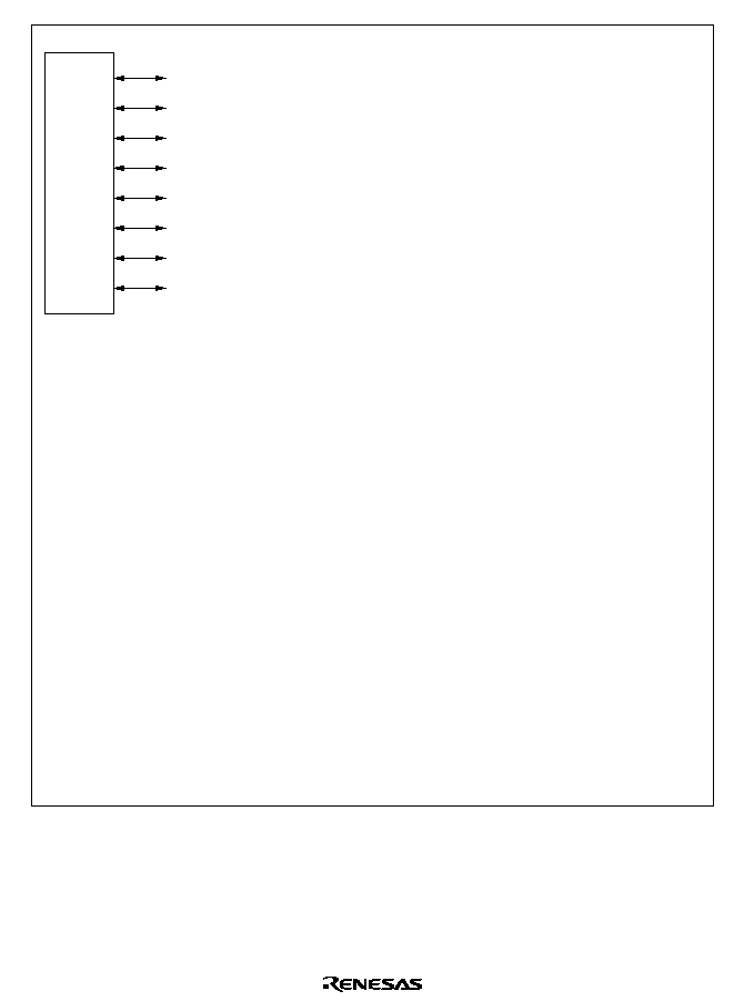
302
Port B
PB
7
/TP /RxD
2
15
PB
6
/TP /TxD
2
14
PB
5
/TP /SCK
2
/
LCAS
13
PB
4
/TP /
UCAS
12
PB
3
/TP /TMIO
3
/
DREQ
1
/
CS
4
11
PB
2
/TP /TMO
2
/
CS
5
10
PB
1
/TP /TMIO
1
/
DREQ
0
/
CS
6
9
PB
0
/TP /TMO
0
/
CS
7
8
Port B pins
PB
7
(input/output)/TP
15
(output) /RxD
2
(input)
PB
6
(input/output)/TP
14
(output) /TxD
2
(output)
PB
5
(input/output)/TP
13
(output) /SCK
2
(input/output) /
LCAS
(output)
PB
4
(input/output)/TP
12
(output) /
UCAS
(output)
PB
3
(input/output)/TP
11
(output) /TMIO
3
(input/output) /
DREQ
1
(input)
CS
4
(output)
PB
2
(input/output)/TP
10
(output) /TMO
2
(output) /
CS
5
(output)
PB
1
(input/output)/TP
9
(output) /TMIO
1
(input/output) /
DREQ
0
(input) /
CS
6
(output)
PB
0
(input/output)/TP
8
(output) /TMO
0
(output) /
CS
7
(output)
Pin functions in modes 1 to 5
PB
7
(input/output)/TP
15
(output) /RxD
2
(input)
PB
6
(input/output)/TP
14
(output) /TxD
2
(output)
PB
5
(input/output)/TP
13
(output) /SCK
2
(input/output)
PB
4
(input/output)/TP
12
(output)
PB
3
(input/output)/TP
11
(output) /TMIO
3
(input/output) /
DREQ
1
(input)
PB
2
(input/output)/TP
10
(output) /TMO
2
(output)
PB
1
(input/output)/TP
9
(output) /TMIO
1
(input/output) /
DREQ
0
(input)
PB
0
(input/output)/TP
8
(output) /TMO
0
(output)
Pin functions in mode 7
Figure 8.11 Port B Pin Configuration
303
8.12.2
Register Descriptions
Table 8.22 summarizes the registers of port B.
Table 8.22
Port B Registers
Address
*
Name
Abbreviation
R/W
Initial Value
H'EE00A
Port B data direction register
PBDDR
W
H'00
H'FFFDA
Port B data register
PBDR
R/W
H'00
Note:
*
Lower 20 bits of the address in advanced mode.
Port B Data Direction Register (PBDDR): PBDDR is an 8-bit write-only register that can select
input or output for each pin in port B. When pins are used for TPC output, the corresponding
PBDDR bits must also be set.
Bit
Initial value
Read/Write
7
PB DDR
0
W
Port B data direction 7 to 0
These bits select input or output for port B pins
7
6
PB DDR
0
W
6
5
PB DDR
0
W
5
4
PB DDR
0
W
4
3
PB DDR
0
W
3
2
PB DDR
0
W
2
1
PB DDR
0
W
1
0
PB DDR
0
W
0
The pin functions that can be selected for port B differ between modes 1 to 5, and mode 7. For the
method of selecting the pin functions, see tables 8.23 and 8.24.
When port B functions as an input/output port, a pin in port B becomes an output port if the
corresponding PBDDR bit is set to 1, and an input port if this bit is cleared to 0.
PBDDR is a write-only register. Its value cannot be read. All bits return 1 when read.
PBDDR is initialized to H'00 by a reset and in hardware standby mode. In software standby mode
it retains its previous setting. Therefore, if a transition is made to software standby mode while
port B is functioning as an input/output port and a PBDDR bit is set to 1, the corresponding pin
maintains its output state.

304
Port B Data Register (PBDR): PBDR is an 8-bit readable/writable register that stores output data
for pins port B. When port B functions as an output port, the value of this register is output. When
a bit in PBDDR is set to 1, if port B is read the value of the corresponding PBDR bit is returned.
When a bit in PBDDR is cleared to 0, if port B is read the corresponding pin logic level is read.
Bit
Initial value
Read/Write
0
PB
0
R/W
0
1
PB
0
R/W
1
2
PB
0
R/W
2
3
PB
0
R/W
3
4
PB
0
R/W
4
5
PB
0
R/W
5
6
PB
0
R/W
6
7
PB
0
R/W
7
Port B data 7 to 0
These bits store data for port B pins
PBDR is initialized to H'00 by a reset and in hardware standby mode. In software standby mode it
retains its previous setting.
305
Table 8.23
Port B Pin Functions (Modes 1 to 5)
Pin
Pin Functions and Selection Method
PB
7
/TP
15
/
RxD
2
Bit RE in SCR of SCI2, bit SMIF in SCMR, bit NDER15 in NDERB, and bit PB
7
DDR select the pin function as
follows.
SMIF
0
1
RE
0
1
--
PB
7
DDR
0
1
1
--
--
NDER15
--
0
1
--
--
Pin function
PB
7
input
PB
7
output
TP
15
output
RxD
2
input
RxD
2
input
PB
6
/TP
14
/
TxD
2
Bit TE in SCR of SCI2, bit SMIF in SCMR, bit NDER14 in NDERB, and bit PB
6
DDR select the pin function as
follows.
SMIF
0
1
TE
0
1
--
PB
6
DDR
0
1
1
--
--
NDER14
--
0
1
--
--
Pin function
PB
6
input
PB
6
output
TP
14
output
TxD
2
output
TxD
2
output
*
Note:
*
Functions as the TxD
2
output pin, but there are two states: one in which the pin is driven, and another
in which the pin is at high-impedance.
PB
5
/TP
13
/
SCK
2
/
LCAS
Bit C/
A
in SMR of SCI2, bits CKE0 and CKE1 in SCR, bit NDER13 in NDERB, and bit PB
5
DDR select the pin
function as follows.
CKE1
0
1
C/
A
0
1
--
CKE0
0
1
--
--
PB
5
DDR
0
1
1
--
--
--
NDER13
--
0
1
--
--
--
Pin function
PB
5
input
PB
5
output
TP
13
output
SCK
2
output
SCK
2
output
SCK
2
input
LCAS
output
*
Note:
*
LCAS
output depending on bits DRAS2 to DRAS0 in DRCRA and bit CSEL in DRCRB, and
regardless of bits C/
A
, CKE0 and CKE1, NDER13, and PB
5
DDR. For details, see section 6, Bus
Controller
.
PB
4
/TP
12
/
Bit NDER12 in NDERB and bit PB
4
DDR select the pin function as follows.
UCAS
PB
4
DDR
0
1
1
NDER12
--
0
1
Pin function
PB
4
input
PB
4
output
TP
12
output
UCAS
output
*
Note:
*
UCAS
output depending on bits DRAS2 to DRAS0 in DRCRA and bit CSEL in DRCRB, and
regardless of bits NDER12 and PB
4
DDR. For details, see section 6, Bus Controller.
306
Pin
Pin Functions and Selection Method
PB
3
/TP
11
/
TMIO
3
/
DREQ
1
/
CS
4
The DRAM interface settings by bits DRAS2 to DRAS0 in DRCRA, bits OIS3/2 and OS1/0 in 8TCSR3, bits
CCLR1 and CCLR0 in 8TCR3, bit CS4E in CSCR, bit NDER11 in NDERB, and bit PB
3
DDR select the pin
function as follows.
DRAM interface
settings
(1) in table below
(2) in table
below
OIS3/2 and OS1/0
All 0
Not all 0
--
CS4E
0
1
--
--
PB
3
DDR
0
1
1
--
--
--
NDER11
--
0
1
--
--
--
Pin function
PB
3
input
PB
3
output
TP
11
output
CS
4
output
TMIO
3
output
CS
4
output
*
3
TMIO
3
input
*
1
DREQ
1
input
*
2
Notes:
*
1 TMIO
3
input when CCLR1 = CCLR0 = 1.
*
2 When an external request is specified as a DMAC activation source,
DREQ
1
input regardless of
bits OIS3 and OIS2, OS1 and OS0, CCLR1 and CCLR0, CS4E, NDER11, and PB
3
DDR.
*
3
CS
4
is output as
RAS
4
.
DRAM interface
settings
(1)
(2)
(1)
DRAS2
0
1
DRAS1
0
1
0
1
DRAS0
0
1
0
1
0
1
0
1
PB
2
/TP
10
/
TMO
2
/
CS
5
The DRAM interface settings by bits DRAS2 to DRAS0 in DRCRA, bits OIS3/2 and OS1/0 in 8TCSR2, bit
CS5E in CSCR, bit NDER10 in NDERB, and bit PB
2
DDR select the pin function as follows.
DRAM interface
settings
(1) in table below
(2) in table
below
OIS3/2 and OS1/0
All 0
Not all 0
--
CS5E
0
1
--
--
PB
2
DDR
0
1
1
--
--
--
NDER10
--
0
1
--
--
--
Pin function
PB
2
input
PB
2
output
TP
10
output
CS
5
output
TMIO
2
output
CS
5
output
*
Note:
*
CS
5
is output as
RAS
5
.
DRAM interface
settings
(1)
(2)
(1)
DRAS2
0
1
DRAS1
0
1
0
1
DRAS0
0
1
0
1
0
1
0
1
307
Pin
Pin Functions and Selection Method
PB
1
/TP
9
/
TMIO
1
/
DREQ
0
/
CS
6
Bits OIS3/2 and OS1/0 in 8TCSR1, bits CCLR1 and CCLR0 in TCR1, bit CS6E in CSCR, bit NDER9 in
NDERB, and bit PB
1
DDR select the pin function as follows.
OIS3/2 and OS1/0
All 0
Not all 0
CS6E
0
1
--
PB
1
DDR
0
1
1
--
--
NDER9
--
0
1
--
--
Pin function
PB
1
input
PB
1
output
TP
9
output
CS
6
output
TMIO
1
output
TMIO
1
input
*
1
DREQ
0
input
*
2
Notes:
*
1 TMIO
1
input when CCLR1 = CCLR0 = 1.
*
2 When an external request is specified as a DMAC activation source,
DREQ
0
input regardless of
bits OIS3/2 and OS1/0, bits CCLR1/0, bit CS6E, bit NDER9, and bit PB
1
DDR.
PB
0
/TP
8
/
TMO
0
/
CS
7
Bits OIS3/2 and OS1/0 in 8TCSR0, bit CS7E in CSCR, bit NDER8 in NDERB, and bit PB
0
DDR select the pin
function as follows.
OIS3/2 and OS1/0
All 0
Not all 0
CS7E
0
1
--
PB
0
DDR
0
1
1
--
--
NDER8
--
0
1
--
--
Pin function
PB
0
input
PB
0
output
TP
8
output
CS
7
output
TMO
0
output
308
Table 8.24
Port B Pin Functions (Mode 7)
Pin
Pin Functions and Selection Method
PB
7
/TP
15
/
RxD
2
Bit RE in SCR of SCI2, bit SMIF in SCMR, bit NDER15 in NDERB, and bit PB
7
DDR select the pin function as
follows.
SMIF
0
1
RE
0
1
--
PB
7
DDR
0
1
1
--
--
NDER15
--
0
1
--
--
Pin function
PB
7
input
PB
7
output
TP
15
output
RxD
2
input
RxD
2
input
PB
6
/TP
14
/
TxD
2
Bit TE in SCR of SCI2, bit SMIF in SCMR, bit NDER14 in NDERB, and bit PB
6
DDR select the pin function as
follows.
SMIF
0
1
TE
0
1
--
PB
6
DDR
0
1
1
--
--
NDER14
--
0
1
--
--
Pin function
PB
6
input
PB
6
output
TP
14
output
TxD
2
output
TxD
2
output
*
Note:
*
Functions as the TxD2 output pin, but there are two states: one in which the pin is driven, and
another in which the pin is at high-impedance.
PB
5
/TP
13
/
SCK
2
Bit C/
A
in SMR of SCI2, bits CKE0 and CKE1 in SCR, bit NDER13 in NDERB, and bit PB
5
DDR select the pin
function as follows.
CKE1
0
1
C/
A
0
1
--
CKE0
0
1
--
--
PB
5
DDR
0
1
1
--
--
--
NDER13
--
0
1
--
--
--
Pin function
PB
5
input
PB
5
output
TP
13
output
SCK
2
output
SCK
2
output
SCK
2
input
PB
4
/TP
12
Bit NDER12 in NDERB and bit PB
4
DDR select the pin function as follows.
PB
4
DDR
0
1
1
NDER12
--
0
1
Pin function
PB
4
input
PB
4
output
TP
12
output
309
Pin
Pin Functions and Selection Method
PB
3
/TP
11
/
TMIO
3
/
Bits OIS3/2 and OS1/0 in 8TCSR3, bits CCLR1 and CCLR0 in 8TCR3, bit NDER11 in NDERB, and bit
PB
3
DDR select the pin function as follows.
DREQ
1
OIS3/2 and OS1/0
All 0
Not all 0
PB
3
DDR
0
1
1
--
NDER11
--
0
1
--
Pin function
PB
3
input
PB
3
output
TP
11
output
TMIO
3
output
TMIO
3
input
*
1
DREQ
1
input
*
2
Notes:
*
1 TMIO
3
input when CCLR1 = CCLR0 = 1.
*
2 When an external request is specified as a DMAC activation source,
DREQ
1
input regardless of
bits OIS3/2 and OS1/0, bit NDER11, and bit PB
3
DDR.
PB
2
/TP
10
/
TMO
2
Bits OIS3/2 and OS1/0 in 8TCSR2, bit NDER10 in NDERB, and bit PB
2
DDR select the pin function as follows.
OIS3/2 and OS1/0
All 0
Not all 0
PB
2
DDR
0
1
1
--
NDER10
--
0
1
--
Pin function
PB
2
input
PB
2
output
TP
10
output
TMO
2
output
PB
1
/TP
9
/
TMIO
1
/
Bits OIS3/2 and OS1/0 in 8TCSR1, bits CCLR1 and CCLR0 in 8TCR0, bit NDER9 in NDERB, and bit PB
1
DDR
select the pin function as follows.
DREQ
0
OIS3/2 and OS1/0
All 0
Not all 0
PB
1
DDR
0
1
1
--
NDER9
--
0
1
--
Pin function
PB
1
input
PB
1
output
TP
9
output
TMIO
1
output
TMIO
1
input
*
1
DREQ
0
input
*
2
Notes:
*
1 TMIO
1
input when CCLR1 = CCLR0 = 1.
*
2 When an external request is specified as a DMAC activation source,
DREQ
0
input regardless of
bits OIS3/2 and OS1/0, bit NDER9, and bit PB
1
DDR.
PB
0
/TP
8
/
Bits OIS3/2 and OS1/0 in 8TCSR0, bit NDER8 in NDERB, and bit PB
0
DDR select the pin function as follows.
TMO
0
OIS3/2 and OS1/0
All 0
Not all 0
PB
0
DDR
0
1
1
--
NDER8
--
0
1
--
Pin function
PB
0
input
PB
0
output
TP
8
output
TMO
0
output

310

311
Section 9 16-Bit Timer
9.1
Overview
The H8/3069F has built-in 16-bit timer module with three 16-bit counter channels.
9.1.1
Features
16-bit timer features are listed below.
�
Capability to process up to 6 pulse outputs or 6 pulse inputs
�
Six general registers (GRs, two per channel) with independently-assignable output compare or
input capture functions
�
Selection of eight counter clock sources for each channel:
Internal clocks:
,
/2,
/4,
/8
External clocks: TCLKA, TCLKB, TCLKC, TCLKD
�
Five operating modes selectable in all channels:
Waveform output by compare match
Selection of 0 output, 1 output, or toggle output (only 0 or 1 output in channel 2)
Input capture function
Rising edge, falling edge, or both edges (selectable)
Counter clearing function
Counters can be cleared by compare match or input capture.
Synchronization
Two or more timer counters (16TCNTs) can be preset simultaneously, or cleared
simultaneously by compare match or input capture. Counter synchronization enables
synchronous register input and output.
PWM mode
PWM output can be provided with an arbitrary duty cycle. With synchronization, up to
three-phase PWM output is possible.
�
Phase counting mode selectable in channel 2
Two-phase encoder output can be counted automatically.
�
High-speed access via internal 16-bit bus
The 16TCNTs and GRs can be accessed at high speed via a 16-bit bus.
�
Any initial timer output value can be set
�
Nine interrupt sources
Each channel has two compare match/input capture interrupts and an overflow interrupt. All
interrupts can be requested independently.

312
�
Output triggering of programmable timing pattern controller (TPC)
Compare match/input capture signals from channels 0 to 2 can be used as TPC output triggers.
Table 9.1 summarizes the 16-bit timer functions.
Table 9.1
16-bit timer Functions
Item
Channel 0
Channel 1
Channel 2
Clock sources
Internal clocks:
,
/2,
/4,
/8
External clocks: TCLKA, TCLKB, TCLKC, TCLKD, selectable
independently
General registers (output
compare/input
capture registers)
GRA0, GRB0
GRA1, GRB1
GRA2, GRB2
Input/output pins
TIOCA
0
, TIOCB
0
TIOCA
1
, TIOCB
1
TIOCA
2
, TIOCB
2
Counter clearing function
GRA0/GRB0 compare
match or input capture
GRA1/GRB1 compare
match or input capture
GRA2/GRB2 compare
match or input capture
Initial output value setting function
Available
Available
Available
Compare
0
Available
Available
Available
match output
1
Available
Available
Available
Toggle
Available
Available
Not available
Input capture function
Available
Available
Available
Synchronization
Available
Available
Available
PWM mode
Available
Available
Available
Phase counting mode
Not available
Not available
Available
Interrupt sources
Three sources
�
Compare match/input
capture A0
�
Compare match/input
capture B0
�
Overflow
Three sources
�
Compare match/input
capture A1
�
Compare match/input
capture B1
�
Overflow
Three sources
�
Compare match/input
capture A2
�
Compare match/input
capture B2
�
Overflow
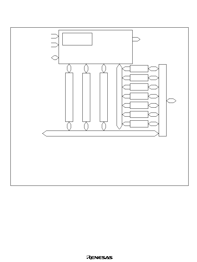
313
9.1.2
Block Diagrams
16-bit timer Block Diagram (Overall): Figure 9.1 is a block diagram of the 16-bit timer.
16-bit timer channel 2
16-bit timer channel 1
16-bit timer channel 0
Module data bus
Bus interface
Internal data bus
IMIA0 to IMIA2
IMIB0 to IMIB2
OVI0 to OVI2
TCLKA to TCLKD
,
/2,
/4,
/8
Clock selector
Control logic
TIOCA
0
to TIOCA
2
TIOCB
0
to TIOCB
2
TSTR
TSNR
TMDR
TOLR
TISRA
TISRB
TISRC
Legend:
TSTR: Timer start register (8 bits)
TSNR: Timer synchro register (8 bits)
TMDR: Timer mode register (8 bits)
TOLR: Timer output level setting register (8 bits)
TISRA: Timer interrupt status register A (8 bits)
TISRB: Timer interrupt status register B (8 bits)
TISRC: Timer interrupt status register C (8 bits)
Figure 9.1 16-bit timer Block Diagram (Overall)
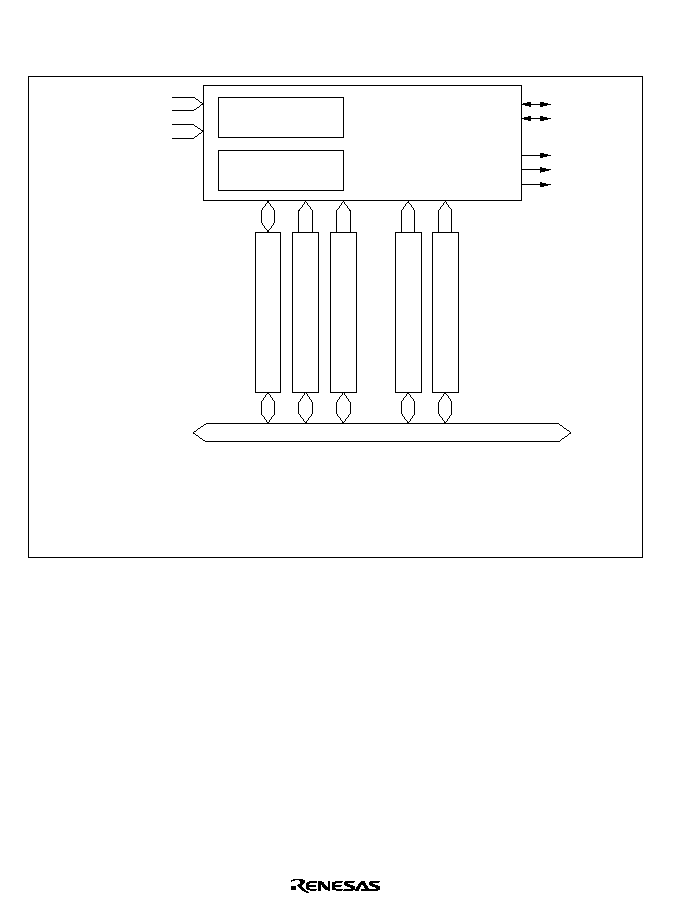
314
Block Diagram of Channels 0 and 1: 16-bit timer channels 0 and 1 are functionally identical.
Both have the structure shown in figure 9.2.
Clock selector
Comparator
Control logic
TCLKA to TCLKD
,
/2,
/4,
/8
TIOCA
0
TIOCB
0
IMIA0
IMIB0
OVI0
16TCNT
GRA
GRB
16TCR
TIOR
Module data bus
Legend:
16TCNT:
GRA, GRB:
TCR:
TIOR:
Timer counter (16 bits)
General registers A and B (input capture/output compare registers) (16 bits 2)
Timer control register (8 bits)
Timer I/O control register (8 bits)
�
Figure 9.2 Block Diagram of Channels 0 and 1
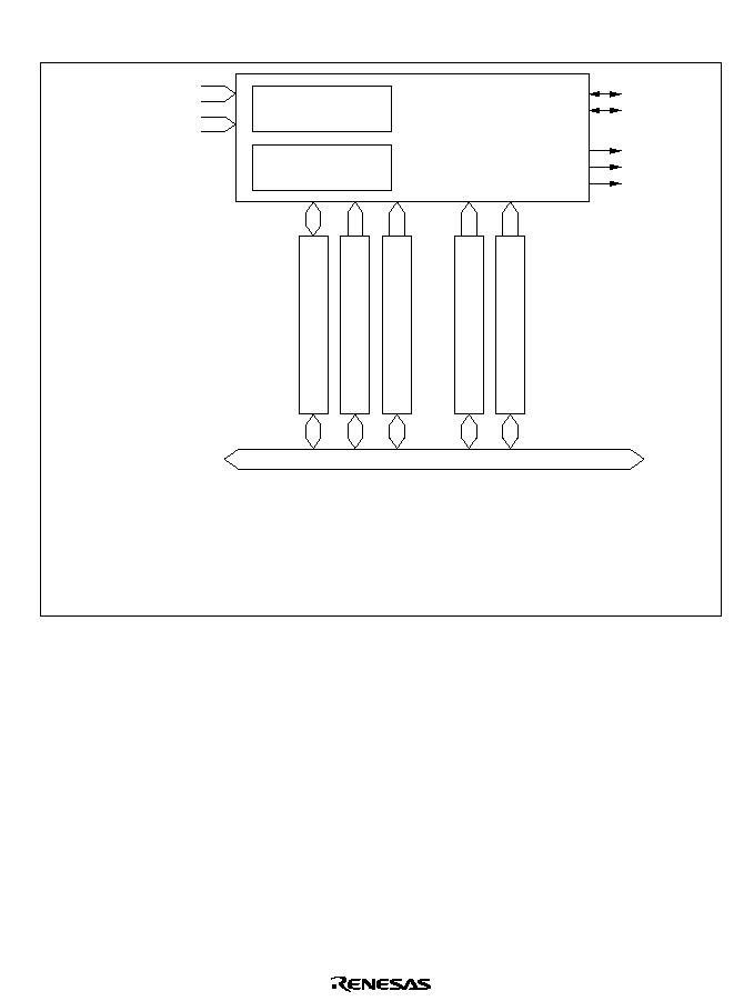
315
Block Diagram of Channel 2: Figure 9.3 is a block diagram of channel 2
Clock selector
Comparator
Control logic
TCLKA to TCLKD
,
/2,
/4,
/8
TIOCA
2
TIOCB
2
IMIA2
IMIB2
OVI2
16TCNT2
GRA2
GRB2
16TCR2
TIOR2
Module data bus
Legend:
16TCNT2:
GRA2, GRB2:
TCR2:
TIOR2:
Timer counter 2 (16 bits)
General registers A2 and B2 (input capture/output compare registers)
(16 bits
�
2)
Timer control register 2 (8 bits)
Timer I/O control register 2 (8 bits)
Figure 9.3 Block Diagram of Channel 2

316
9.1.3
Pin Configuration
Table 9.2 summarizes the 16-bit timer pins.
Table 9.2
16-bit timer Pins
Channel
Name
Abbre-
viation
Input/
Output
Function
Common Clock input A
TCLKA
Input
External clock A input pin
(phase-A input pin in phase counting mode)
Clock input B
TCLKB
Input
External clock B input pin
(phase-B input pin in phase counting mode)
Clock input C
TCLKC
Input
External clock C input pin
Clock input D
TCLKD
Input
External clock D input pin
0
Input capture/output
compare A0
TIOCA
0
Input/
output
GRA0 output compare or input capture pin
PWM output pin in PWM mode
Input capture/output
compare B0
TIOCB
0
Input/
output
GRB0 output compare or input capture pin
1
Input capture/output
compare A1
TIOCA
1
Input/
output
GRA1 output compare or input capture pin
PWM output pin in PWM mode
Input capture/output
compare B1
TIOCB
1
Input/
output
GRB1 output compare or input capture pin
2
Input capture/output
compare A2
TIOCA
2
Input/
output
GRA2 output compare or input capture pin
PWM output pin in PWM mode
Input capture/output
compare B2
TIOCB
2
Input/
output
GRB2 output compare or input capture pin

317
9.1.4
Register Configuration
Table 9.3 summarizes the 16-bit timer registers.
Table 9.3
16-bit timer Registers
Channel
Address
*
1
Name
Abbre-
viation
R/W
Initial
Value
Common
H'FFF60
Timer start register
TSTR
R/W
H'F8
H'FFF61
Timer synchro register
TSNC
R/W
H'F8
H'FFF62
Timer mode register
TMDR
R/W
H'98
H'FFF63
Timer output level setting register
TOLR
W
H'C0
H'FFF64
Timer interrupt status register A
TISRA
R/(W)
*
2
H'88
H'FFF65
Timer interrupt status register B
TISRB
R/(W)
*
2
H'88
H'FFF66
Timer interrupt status register C
TISRC
R/(W)
*
2
H'88
0
H'FFF68
Timer control register 0
16TCR0
R/W
H'80
H'FFF69
Timer I/O control register 0
TIOR0
R/W
H'88
H'FFF6A
Timer counter 0H
16TCNT0H R/W
H'00
H'FFF6B
Timer counter 0L
16TCNT0L R/W
H'00
H'FFF6C
General register A0H
GRA0H
R/W
H'FF
H'FFF6D
General register A0L
GRA0L
R/W
H'FF
H'FFF6E
General register B0H
GRB0H
R/W
H'FF
H'FFF6F
General register B0L
GRB0L
R/W
H'FF
1
H'FFF70
Timer control register 1
16TCR1
R/W
H'80
H'FFF71
Timer I/O control register 1
TIOR1
R/W
H'88
H'FFF72
Timer counter 1H
16TCNT1H R/W
H'00
H'FFF73
Timer counter 1L
16TCNT1L R/W
H'00
H'FFF74
General register A1H
GRA1H
R/W
H'FF
H'FFF75
General register A1L
GRA1L
R/W
H'FF
H'FFF76
General register B1H
GRB1H
R/W
H'FF
H'FFF77
General register B1L
GRB1L
R/W
H'FF
318
Channel
Address
*
1
Name
Abbre-
viation
R/W
Initial
Value
2
H'FFF78
Timer control register 2
16TCR2
R/W
H'80
H'FFF79
Timer I/O control register 2
TIOR2
R/W
H'88
H'FFF7A
Timer counter 2H
16TCNT2H R/W
H'00
H'FFF7B
Timer counter 2L
16TCNT2L R/W
H'00
H'FFF7C
General register A2H
GRA2H
R/W
H'FF
H'FFF7D
General register A2L
GRA2L
R/W
H'FF
H'FFF7E
General register B2H
GRB2H
R/W
H'FF
H'FFF7F
General register B2L
GRB2L
R/W
H'FF
Notes:
*
1 The lower 20 bits of the address in advanced mode are indicated.
*
2 Only 0 can be written in bits 3 to 0, to clear the flags.
9.2
Register Descriptions
9.2.1
Timer Start Register (TSTR)
TSTR is an 8-bit readable/writable register that starts and stops the timer counter (16TCNT) in
channels 0 to 2.
Bit
Initial value
Read/Write
7
--
1
--
6
--
1
--
5
--
1
--
4
--
1
--
3
--
1
--
2
STR2
0
R/W
1
STR1
0
R/W
0
STR0
0
R/W
Reserved bits
Counter start 2 to 0
These bits start and
stop 16TCNT2 to 16TCNT0
TSTR is initialized to H'F8 by a reset and in standby mode.
Bits 7 to 3--Reserved: These bits cannot be modified and are always read as 1.
Bit 2--Counter Start 2 (STR2): Starts and stops timer counter 2 (16TCNT2).
Bit 2
STR2
Description
0
16TCNT2 is halted
(Initial value)
1
16TCNT2 is counting
319
Bit 1--Counter Start 1 (STR1): Starts and stops timer counter 1 (16TCNT1).
Bit 1
STR1
Description
0
16TCNT1 is halted
(Initial value)
1
16TCNT1 is counting
Bit 0--Counter Start 0 (STR0): Starts and stops timer counter 0 (16TCNT0).
Bit 0
STR0
Description
0
16TCNT0 is halted
(Initial value)
1
16TCNT0 is counting
9.2.2
Timer Synchro Register (TSNC)
TSNC is an 8-bit readable/writable register that selects whether channels 0 to 2 operate
independently or synchronously. Channels are synchronized by setting the corresponding bits to 1.
Bit
Initial value
Read/Write
7
--
1
--
6
--
1
--
5
--
1
--
4
--
1
--
3
--
1
--
2
SYNC2
0
R/W
1
SYNC1
0
R/W
0
SYNC0
0
R/W
Reserved bits
Timer sync 2 to 0
These bits synchronize
channels 2 to 0
TSNC is initialized to H'F8 by a reset and in standby mode.
Bits 7 to 3--Reserved: These bits cannot be modified and are always read as 1.
Bit 2--Timer Sync 2 (SYNC2): Selects whether channel 2 operates independently or
synchronously.
Bit 2
SYNC2
Description
0
Channel 2's timer counter (16TCNT2) operates independently
(Initial value)
16TCNT2 is preset and cleared independently of other channels
1
Channel 2 operates synchronously
16TCNT2 can be synchronously preset and cleared

320
Bit 1--Timer Sync 1 (SYNC1): Selects whether channel 1 operates independently or
synchronously.
Bit 1
SYNC1
Description
0
Channel 1's timer counter (16TCNT1) operates independently
(Initial value)
16TCNT1 is preset and cleared independently of other channels
1
Channel 1 operates synchronously
16TCNT1 can be synchronously preset and cleared
Bit 0--Timer Sync 0 (SYNC0): Selects whether channel 0 operates independently or
synchronously.
Bit 0
SYNC0
Description
0
Channel 0's timer counter (16TCNT0) operates independently
(Initial value)
16TCNT0 is preset and cleared independently of other channels
1
Channel 0 operates synchronously
16TCNT0 can be synchronously preset and cleared
9.2.3
Timer Mode Register (TMDR)
TMDR is an 8-bit readable/writable register that selects PWM mode for channels 0 to 2. It also
selects phase counting mode and the overflow flag (OVF) setting conditions for channel 2.
Bit
Initial value
Read/Write
7
--
1
--
6
MDF
0
R/W
5
FDIR
0
R/W
4
--
1
--
3
--
1
--
0
PWM0
0
R/W
2
PWM2
0
R/W
1
PWM1
0
R/W
Reserved bit
Reserved bit
PWM mode 2 to 0
These bits select PWM
mode for channels 2 to 0
Phase counting mode flag
Selects phase counting mode for channel 2
Flag direction
Selects the setting condition for the overflow
flag (OVF) in TISRC
TMDR is initialized to H'98 by a reset and in standby mode.
321
Bit 7--Reserved: This bit cannot be modified and is always read as 1.
Bit 6--Phase Counting Mode Flag (MDF): Selects whether channel 2 operates normally or in
phase counting mode.
Bit 6
MDF
Description
0
Channel 2 operates normally
(Initial value)
1
Channel 2 operates in phase counting mode
When MDF is set to 1 to select phase counting mode, 16TCNT2 operates as an up/down-counter
and pins TCLKA and TCLKB become counter clock input pins. 16TCNT2 counts both rising and
falling edges of TCLKA and TCLKB, and counts up or down as follows.
Counting
Direction
Down-Counting
Up-Counting
TCLKA pin
High
Low
Low
High
TCLKB pin
Low
High
High
Low
In phase counting mode, external clock edge selection by bits CKEG1 and CKEG0 in 16TCR2
and counter clock selection by bits TPSC2 to TPSC0 are invalid, and the above phase counting
mode operations take precedence.
The counter clearing condition selected by the CCLR1 and CCLR0 bits in 16TCR2 and the
compare match/input capture settings and interrupt functions of TIOR2, TISRA, TISRB, TISRC
remain effective in phase counting mode.
Bit 5--Flag Direction (FDIR): Designates the setting condition for the OVF flag in TISRC. The
FDIR designation is valid in all modes in channel 2.
Bit 5
FDIR
Description
0
OVF is set to 1 in TISRC when 16TCNT2 overflows or underflows
(Initial value)
1
OVF is set to 1 in TISRC when 16TCNT2 overflows
Bits 4 and 3--Reserved: These bits cannot be modified and are always read as 1.

322
Bit 2--PWM Mode 2 (PWM2): Selects whether channel 2 operates normally or in PWM mode.
Bit 2
PWM2
Description
0
Channel 2 operates normally
(Initial value)
1
Channel 2 operates in PWM mode
When bit PWM2 is set to 1 to select PWM mode, pin TIOCA
2
becomes a PWM output pin. The
output goes to 1 at compare match with GRA2, and to 0 at compare match with GRB2.
Bit 1--PWM Mode 1 (PWM1): Selects whether channel 1 operates normally or in PWM mode.
Bit 1
PWM1
Description
0
Channel 1 operates normally
(Initial value)
1
Channel 1 operates in PWM mode
When bit PWM1 is set to 1 to select PWM mode, pin TIOCA
1
becomes a PWM output pin. The
output goes to 1 at compare match with GRA1, and to 0 at compare match with GRB1.
Bit 0--PWM Mode 0 (PWM0): Selects whether channel 0 operates normally or in PWM mode.
Bit 0
PWM0
Description
0
Channel 0 operates normally
(Initial value)
1
Channel 0 operates in PWM mode
When bit PWM0 is set to 1 to select PWM mode, pin TIOCA
0
becomes a PWM output pin. The
output goes to 1 at compare match with GRA0, and to 0 at compare match with GRB0.
323
9.2.4
Timer Interrupt Status Register A (TISRA)
TISRA is an 8-bit readable/writable register that indicates GRA compare match or input capture
and enables or disables GRA compare match and input capture interrupt requests.
7
--
1
--
Bit
Initial value
Read/Write
6
IMIEA2
0
R/W
5
IMIEA1
0
R/W
4
IMIEA0
0
R/W
3
--
1
--
2
IMFA2
0
R/(W)
*
1
IMFA1
0
R/(W)
*
0
IMFA0
0
R/(W)
*
Reserved bit
Reserved bit
Input capture/compare match interrupt enable A2 to A0
These bits enable or disable interrupts by the IMFA flags
Input capture/compare match
flags A2 to A0
Status flags indicating GRA
compare match or input capture
Note:
*
Only 0 can be written, to clear the flag.
TISRA is initialized to H'88 by a reset and in standby mode.
Bit 7--Reserved: This bit cannot be modified and is always read as 1.
Bit 6--Input Capture/Compare Match Interrupt Enable A2 (IMIEA2): Enables or disables
the interrupt requested by the IMFA2 when IMFA2 flag is set to 1.
Bit 6
IMIEA2
Description
0
IMIA2 interrupt requested by IMFA2 flag is disabled
(Initial value)
1
IMIA2 interrupt requested by IMFA2 flag is enabled

324
Bit 5--Input Capture/Compare Match Interrupt Enable A1 (IMIEA1): Enables or disables
the interrupt requested by the IMFA1 flag when IMFA1 is set to 1.
Bit 5
IMIEA1
Description
0
IMIA1 interrupt requested by IMFA1 flag is disabled
(Initial value)
1
IMIA1 interrupt requested by IMFA1 flag is enabled
Bit 4--Input Capture/Compare Match Interrupt Enable A0 (IMIEA0): Enables or disables
the interrupt requested by the IMFA0 flag when IMFA0 is set to 1.
Bit 4
IMIEA0
Description
0
IMIA0 interrupt requested by IMFA0 flag is disabled
(Initial value)
1
IMIA0 interrupt requested by IMFA0 flag is enabled
Bit 3--Reserved: This bit cannot be modified and is always read as 1.
Bit 2--Input Capture/Compare Match Flag A2 (IMFA2): This status flag indicates GRA2
compare match or input capture events.
Bit 2
IMFA2
Description
0
[Clearing condition]
(Initial value)
Read IMFA2 flag when IMFA2 =1, then write 0 in IMFA2 flag
1
[Setting conditions]
�
16TCNT2 = GRA2 when GRA2 functions as an output compare register
�
16TCNT2 value is transferred to GRA2 by an input capture signal when GRA2
functions as an input capture register

325
Bit 1--Input Capture/Compare Match Flag A1 (IMFA1): This status flag indicates GRA1
compare match or input capture events.
Bit 1
IMFA1
Description
0
[Clearing condition]
(Initial value)
Read IMFA1 flag when IMFA1 =1, then write 0 in IMFA1 flag
1
[Setting conditions]
�
16TCNT1 = GRA1 when GRA1 functions as an output compare register
�
16TCNT1 value is transferred to GRA1 by an input capture signal when GRA1
functions as an input capture register
Bit 0--Input Capture/Compare Match Flag A0 (IMFA0): This status flag indicates GRA0
compare match or input capture events.
Bit 0
IMFA0
Description
0
[Clearing condition]
(Initial value)
Read IMFA0 flag when IMFA0 =1, then write 0 in IMFA0 flag
1
[Setting conditions]
�
16TCNT0 = GRA0 when GRA0 functions as an output compare register
�
16TCNT0 value is transferred to GRA0 by an input capture signal when GRA0
functions as an input capture register
326
9.2.5
Timer Interrupt Status Register B (TISRB)
TISRB is an 8-bit readable/writable register that indicates GRB compare match or input capture
and enables or disables GRB compare match and input capture interrupt requests.
7
--
1
--
Bit
Initial value
Read/Write
6
IMIEB2
0
R/W
5
IMIEB1
0
R/W
4
IMIEB0
0
R/W
3
--
1
--
2
IMFB2
0
R/(W)
*
1
IMFB1
0
R/(W)
*
0
IMFB0
0
R/(W)
*
Reserved bit
Reserved bit
Input capture/compare match interrupt enable B2 to B0
These bits enable or disable interrupts by the IMFB flags
Input capture/compare match
flags B2 to B0
Status flags indicating GRB
compare match or input capture
Note:
*
Only 0 can be written, to clear the flag.
TISRB is initialized to H'88 by a reset and in standby mode.
Bit 7--Reserved: This bit cannot be modified and is always read as 1.
Bit 6--Input Capture/Compare Match Interrupt Enable B2 (IMIEB2): Enables or disables
the interrupt requested by the IMFB2 when IMFB2 flag is set to 1.
Bit 6
IMIEB2
Description
0
IMIB2 interrupt requested by IMFB2 flag is disabled
(Initial value)
1
IMIB2 interrupt requested by IMFB2 flag is enabled

327
Bit 5--Input Capture/Compare Match Interrupt Enable B1 (IMIEB1): Enables or disables
the interrupt requested by the IMFB1 when IMFB1 flag is set to 1.
Bit 5
IMIEB1
Description
0
IMIB1 interrupt requested by IMFB1 flag is disabled
(Initial value)
1
IMIB1 interrupt requested by IMFB1 flag is enabled
Bit 4--Input Capture/Compare Match Interrupt Enable B0 (IMIEB0): Enables or disables
the interrupt requested by the IMFB0 when IMFB0 flag is set to 1.
Bit 4
IMIEB0
Description
0
IMIB0 interrupt requested by IMFB0 flag is disabled
(Initial value)
1
IMIB0 interrupt requested by IMFB0 flag is enabled
Bit 3--Reserved: This bit cannot be modified and is always read as 1.
Bit 2--Input Capture/Compare Match Flag B2 (IMFB2): This status flag indicates GRB2
compare match or input capture events.
Bit 2
IMFB2
Description
0
[Clearing condition]
(Initial value)
Read IMFB2 flag when IMFB2 =1, then write 0 in IMFB2 flag
1
[Setting conditions]
�
16TCNT2 = GRB2 when GRB2 functions as an output compare register
�
16TCNT2 value is transferred to GRB2 by an input capture signal when GRB2
functions as an input capture register

328
Bit 1--Input Capture/Compare Match Flag B1 (IMFB1): This status flag indicates GRB1
compare match or input capture events.
Bit 1
IMFB1
Description
0
[Clearing condition]
(Initial value)
Read IMFB1 flag when IMFB1 =1, then write 0 in IMFB1 flag
1
[Setting conditions]
�
16TCNT1 = GRB1 when GRB1 functions as an output compare register
�
16TCNT1 value is transferred to GRB1 by an input capture signal when GRB1
functions as an input capture register
Bit 0--Input Capture/Compare Match Flag B0 (IMFB0): This status flag indicates GRB0
compare match or input capture events.
Bit 0
IMFB0
Description
0
[Clearing condition]
(Initial value)
Read IMFB0 flag when IMFB0 =1, then write 0 in IMFB0 flag
1
[Setting conditions]
�
16TCNT0 = GRB0 when GRB0 functions as an output compare register
�
16TCNT0 value is transferred to GRB0 by an input capture signal when GRB0
functions as an input capture register
329
9.2.6
Timer Interrupt Status Register C (TISRC)
TISRC is an 8-bit readable/writable register that indicates 16TCNT overflow or underflow and
enables or disables overflow interrupt requests.
7
--
1
--
Bit
Initial value
Read/Write
6
OVIE2
0
R/W
5
OVIE1
0
R/W
4
OVIE0
0
R/W
3
--
1
--
2
OVF2
0
R/(W)
*
1
OVF1
0
R/(W)
*
0
OVF0
0
R/(W)
*
Reserved bit
Reserved bit
Overflow interrupt enable 2 to 0
These bits enable or disable interrupts by the OVF flags
Overflow flags 2 to 0
Status flags indicating
interrupts by OVF flags
Note:
*
Only 0 can be written, to clear the flag.
TISRC is initialized to H'88 by a reset and in standby mode.
Bit 7--Reserved: This bit cannot be modified and is always read as 1.
Bit 6--Overflow Interrupt Enable 2 (OVIE2): Enables or disables the interrupt requested by the
OVF2 when OVF2 flag is set to 1.
Bit 6
OVIE2
Description
0
OVI2 interrupt requested by OVF2 flag is disabled
(Initial value)
1
OVI2 interrupt requested by OVF2 flag is enabled
Bit 5--Overflow Interrupt Enable 1 (OVIE1): Enables or disables the interrupt requested by the
OVF1 when OVF1 flag is set to 1.
Bit 5
OVIE1
Description
0
OVI1 interrupt requested by OVF1 flag is disabled
(Initial value)
1
OVI1 interrupt requested by OVF1 flag is enabled

330
Bit 4--Overflow Interrupt Enable 0 (OVIE0): Enables or disables the interrupt requested by the
OVF0 when OVF0 flag is set to 1.
Bit 4
OVIE0
Description
0
OVI0 interrupt requested by OVF0 flag is disabled
(Initial value)
1
OVI0 interrupt requested by OVF0 flag is enabled
Bit 3--Reserved: This bit cannot be modified and is always read as 1.
Bit 2--Overflow Flag 2 (OVF2): This status flag indicates 16TCNT2 overflow.
Bit 2
OVF2
Description
0
[Clearing condition]
(Initial value)
Read OVF2 flag when OVF2 =1, then write 0 in OVF2 flag
1
[Setting condition]
16TCNT2 overflowed from H'FFFF to H'0000, or underflowed from H'0000 to H'FFFF
Note:
16TCNT underflow occurs when 16TCNT operates as an up/down-counter. Underflow
occurs only when channel 2 operates in phase counting mode (MDF = 1 in TMDR).
Bit 1--Overflow Flag 1 (OVF1): This status flag indicates 16TCNT1 overflow.
Bit 1
OVF1
Description
0
[Clearing condition]
(Initial value)
Read OVF1 flag when OVF1 =1, then write 0 in OVF1 flag
1
[Setting condition]
16TCNT1 overflowed from H'FFFF to H'0000
Bit 0--Overflow Flag 0 (OVF0): This status flag indicates 16TCNT0 overflow.
Bit 0
OVF0
Description
0
[Clearing condition]
(Initial value)
Read OVF0 flag when OVF0 =1, then write 0 in OVF0 flag
1
[Setting condition]
16TCNT0 overflowed from H'FFFF to H'0000

331
9.2.7
Timer Counters (16TCNT)
16TCNT is a 16-bit counter. The 16-bit timer has three 16TCNTs, one for each channel.
Channel
Abbreviation
Function
0
16TCNT0
Up-counter
1
16TCNT1
2
16TCNT2
Phase counting mode: up/down-counter
Other modes: up-counter
Bit
Initial value
Read/Write
14
0
R/W
12
0
R/W
10
0
R/W
8
0
R/W
6
0
R/W
0
0
R/W
4
0
R/W
2
0
R/W
15
0
R/W
13
0
R/W
11
0
R/W
9
0
R/W
7
0
R/W
1
0
R/W
5
0
R/W
3
0
R/W
Each 16TCNT is a 16-bit readable/writable register that counts pulse inputs from a clock source.
The clock source is selected by bits TPSC2 to TPSC0 in 16TCR.
16TCNT0 and 16TCNT1 are up-counters. 16TCNT2 is an up/down-counter in phase counting
mode and an up-counter in other modes.
16TCNT can be cleared to H'0000 by compare match with GRA or GRB or by input capture to
GRA or GRB (counter clearing function).
When 16TCNT overflows (changes from H'FFFF to H'0000), the OVF flag is set to 1 in TISRC of
the corresponding channel.
When 16TCNT underflows (changes from H'0000 to H'FFFF), the OVF flag is set to 1 in TISRC
of the corresponding channel.
The 16TCNTs are linked to the CPU by an internal 16-bit bus and can be written or read by either
word access or byte access.
Each 16TCNT is initialized to H'0000 by a reset and in standby mode.

332
9.2.8
General Registers (GRA, GRB)
The general registers are 16-bit registers. The 16-bit timer has 6 general registers, two in each
channel.
Channel
Abbreviation
Function
0
GRA0, GRB0
Output compare/input capture register
1
GRA1, GRB1
2
GRA2, GRB2
Bit
Initial value
Read/Write
14
1
R/W
12
1
R/W
10
1
R/W
8
1
R/W
6
1
R/W
0
1
R/W
4
1
R/W
2
1
R/W
15
1
R/W
13
1
R/W
11
1
R/W
9
1
R/W
7
1
R/W
1
1
R/W
5
1
R/W
3
1
R/W
A general register is a 16-bit readable/writable register that can function as either an output
compare register or an input capture register. The function is selected by settings in TIOR.
When a general register is used as an output compare register, its value is constantly compared
with the 16TCNT value. When the two values match (compare match), the IMFA or IMFB flag is
set to 1 in TISRA/TISRB. Compare match output can be selected in TIOR.
When a general register is used as an input capture register, an external input capture signal are
detected and the current 16TCNT value is stored in the general register. The corresponding IMFA
or IMFB flag in TISRA/TISRB is set to 1 at the same time. The edges of the input capture signal
are selected in TIOR.
TIOR settings are ignored in PWM mode.
General registers are linked to the CPU by an internal 16-bit bus and can be written or read by
either word access or byte access.
General registers are set as output compare registers (with no pin output) and initialized to H'FFFF
by a reset and in standby mode.
333
9.2.9
Timer Control Registers (16TCR)
16TCR is an 8-bit register. The 16-bit timer has three 16TCRs, one in each channel.
Channel
Abbreviation
Function
0
1
2
16TCR0
16TCR1
16TCR2
16TCR controls the timer counter. The 16TCRs in all
channels are functionally identical. When phase counting
mode is selected in channel 2, the settings of bits CKEG1
and CKEG0 and TPSC2 to TPSC0 in 16TCR2 are ignored.
Bit
Initial value
Read/Write
7
--
1
--
6
CCLR1
0
R/W
5
CCLR0
0
R/W
4
CKEG1
0
R/W
3
CKEG0
0
R/W
0
TPSC0
0
R/W
2
TPSC2
0
R/W
1
TPSC1
0
R/W
Timer prescaler 2 to 0
These bits select the timer
counter clock
Reserved bit
Clock edge 1/0
These bits select external clock edges
Counter clear 1/0
These bits select the counter clear source
Each 16TCR is an 8-bit readable/writable register that selects the timer counter clock source,
selects the edge or edges of external clock sources, and selects how the counter is cleared.
16TCR is initialized to H'80 by a reset and in standby mode.
Bit 7--Reserved: This bit cannot be modified and is always read as 1.

334
Bits 6 and 5--Counter Clear 1 and 0 (CCLR1, CCLR0): These bits select how 16TCNT is
cleared.
Bit 6
CCLR1
Bit 5
CCLR0
Description
0
0
16TCNT is not cleared
(Initial value)
1
16TCNT is cleared by GRA compare match or input capture
*
1
1
0
16TCNT is cleared by GRB compare match or input capture
*
1
1
Synchronous clear: 16TCNT is cleared in synchronization with other
synchronized timers
*
2
Notes:
*
1 16TCNT is cleared by compare match when the general register functions as an output
compare register, and by input capture when the general register functions as an input
capture register.
*
2 Selected in TSNC.
Bits 4 and 3--Clock Edge 1 and 0 (CKEG1, CKEG0): These bits select external clock input
edges when an external clock source is used.
Bit 4
CKEG1
Bit 3
CKEG0
Description
0
0
Count rising edges
(Initial value)
1
Count falling edges
1
--
Count both edges
When channel 2 is set to phase counting mode, bits CKEG1 and CKEG0 in 16TCR2 are ignored.
Phase counting takes precedence.
Bits 2 to 0--Timer Prescaler 2 to 0 (TPSC2 to TPSC0): These bits select the counter clock of
16TCNT.
Bit 2
TPSC2
Bit 1
TPSC1
Bit 0
TPSC0
Function
0
0
0
Internal clock:
(Initial value)
1
Internal clock:
/2
1
0
Internal clock:
/4
1
Internal clock:
/8
1
0
0
External clock A: TCLKA input
1
External clock B: TCLKB input
1
0
External clock C: TCLKC input
1
External clock D: TCLKD input
335
When bit TPSC2 is cleared to 0 an internal clock source is selected, and the timer counts only
falling edges. When bit TPSC2 is set to 1 an external clock source is selected, and the timer counts
the edges selected by bits CKEG1 and CKEG0.
When channel 2 is set to phase counting mode (MDF = 1 in TMDR), the settings of bits TPSC2 to
TPSC0 in 16TCR2 are ignored. Phase counting takes precedence.
9.2.10
Timer I/O Control Register (TIOR)
TIOR is an 8-bit register. The 16-bit timer has three TIORs, one in each channel.
Channel
Abbreviation
Function
0
TIOR0
TIOR controls the general registers. Some functions differ in PWM
1
TIOR1
mode.
2
TIOR2
Bit
Initial value
Read/Write
7
--
1
--
6
IOB2
0
R/W
5
IOB1
0
R/W
4
IOB0
0
R/W
3
--
1
--
0
IOA0
0
R/W
2
IOA2
0
R/W
1
IOA1
0
R/W
I/O control A2 to A0
These bits select GRA
functions
Reserved bit
I/O control B2 to B0
These bits select GRB functions
Reserved bit
Each TIOR is an 8-bit readable/writable register that selects the output compare or input capture
function for GRA and GRB, and specifies the functions of the TIORA and TIORB pins. If the
output compare function is selected, TIOR also selects the type of output. If input capture is
selected, TIOR also selects the edges of the input capture signal.
TIOR is initialized to H'88 by a reset and in standby mode.
Bit 7--Reserved: This bit cannot be modified and is always read as 1.

336
Bits 6 to 4--I/O Control B2 to B0 (IOB2 to IOB0): These bits select the GRB function.
Bit 6
IOB2
Bit 5
IOB1
Bit 4
IOB0
Function
0
0
0
GRB is an output
No output at compare match
(Initial value)
1
compare register
0 output at GRB compare match
*
1
1
0
1 output at GRB compare match
*
1
1
Output toggles at GRB compare match
(1 output in channel 2)
*
1
*
2
1
0
0
GRB is an input
GRB captures rising edge of input
1
compare register
GRB captures falling edge of input
1
0
GRB captures both edges of input
1
Notes:
*
1 After a reset, the output conforms to the TOLR setting until the first compare match.
*
2 Channel 2 output cannot be toggled by compare match. When this setting is made, 1
output is selected automatically.
Bit 3--Reserved: This bit cannot be modified and is always read as 1.
Bits 2 to 0--I/O Control A2 to A0 (IOA2 to IOA0): These bits select the GRA function.
Bit 2
IOA2
Bit 1
IOA1
Bit 0
IOA0
Function
0
0
0
GRA is an output
No output at compare match
(Initial value)
1
compare register
0 output at GRA compare match
*
1
1
0
1 output at GRA compare match
*
1
1
Output toggles at GRA compare match
(1 output in channel 2)
*
1
*
2
1
0
0
GRA is an input
GRA captures rising edge of input
1
compare register
GRA captures falling edge of input
1
0
GRA captures both edges of input
1
Notes:
*
1 After a reset, the output conforms to the TOLR setting until the first compare match.
*
2 Channel 2 output cannot be toggled by compare match. When this setting is made, 1
output is selected automatically.

337
9.2.11
Timer Output Level Setting Register C (TOLR)
TOLR is an 8-bit write-only register that selects the timer output level for channels 0 to 2.
7
--
1
--
Bit
Initial value
Read/Write
6
--
1
--
5
TOB2
0
W
4
TOA2
0
W
3
TOB1
0
W
2
TOA1
0
W
1
TOB0
0
W
0
TOA0
0
W
Reserved bits
Output level setting A2 to A0, B2 to B0
These bits set the levels of the timer outputs
(TIOCA
2
to TIOCA
0
, and TIOCB
2
to TIOCB
0
)
A TOLR setting can only be made when the corresponding bit in TSTR is 0.
TOLR is a write-only register, and cannot be read. If it is read, all bits will return a value of 1.
TOLR is initialized to H'C0 by a reset and in standby mode.
Bits 7 and 6--Reserved: These bits cannot be modified.
Bit 5--Output Level Setting B2 (TOB2): Sets the value of timer output TIOCB
2
.
Bit 5
TOB2
Description
0
TIOCB
2
is 0
(Initial value)
1
TIOCB
2
is 1
Bit 4--Output Level Setting A2 (TOA2): Sets the value of timer output TIOCA
2
.
Bit 4
TOA2
Description
0
TIOCA
2
is 0
(Initial value)
1
TIOCA
2
is 1

338
Bit 3--Output Level Setting B1 (TOB1): Sets the value of timer output TIOCB
1
.
Bit 3
TOB1
Description
0
TIOCB
1
is 0
(Initial value)
1
TIOCB
1
is 1
Bit 2--Output Level Setting A1 (TOA1): Sets the value of timer output TIOCA
1
.
Bit 2
TOA1
Description
0
TIOCA
1
is 0
(Initial value)
1
TIOCA
1
is 1
Bit 1--Output Level Setting B0 (TOB0): Sets the value of timer output TIOCB
0
.
Bit 0
TOB0
Description
0
TIOCB
0
is 0
(Initial value)
1
TIOCB
0
is 1
Bit 0--Output Level Setting A0 (TOA0): Sets the value of timer output TIOCA
0
.
Bit 0
TOA0
Description
0
TIOCA
0
is 0
(Initial value)
1
TIOCA
0
is 1
339
9.3
CPU Interface
9.3.1
16-Bit Accessible Registers
The timer counters (16TCNTs), general registers A and B (GRAs and GRBs) are 16-bit registers,
and are linked to the CPU by an internal 16-bit data bus. These registers can be written or read a
word at a time, or a byte at a time.
Figures 9.4 and 9.5 show examples of word read/write access to a timer counter (16TCNT).
Figures 9.6 to 9.9 show examples of byte read/write access to 16TCNTH and 16TCNTL.
On-chip data bus
CPU
H
L
Bus interface
H
L
Module
data bus
16TCNTH
16TCNTL
Figure 9.4 16TCNT Access Operation [CPU Writes to 16TCNT, Word]
On-chip data bus
CPU
H
L
Bus interface
H
L
Module
data bus
16TCNTH
16TCNTL
Figure 9.5 Access to Timer Counter (CPU Reads 16TCNT, Word)
340
On-chip data bus
CPU
H
L
Bus interface
H
L
Module
data bus
16TCNTH
16TCNTL
Figure 9.6 Access to Timer Counter H (CPU Writes to 16TCNTH, Upper Byte)
On-chip data bus
CPU
H
L
Bus interface
H
L
Module
data bus
16TCNTH
16TCNTL
Figure 9.7 Access to Timer Counter L (CPU Writes to 16TCNTL, Lower Byte)
On-chip data bus
CPU
H
L
Bus interface
H
L
Module
data bus
16TCNTH
16TCNTL
Figure 9.8 Access to Timer Counter H (CPU Reads 16TCNTH, Upper Byte)
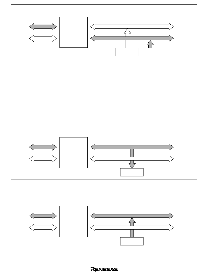
341
On-chip data bus
CPU
H
L
Bus interface
H
L
Module
data bus
16TCNTH
16TCNTL
Figure 9.9 Access to Timer Counter L (CPU Reads 16TCNTL, Lower Byte)
9.3.2
8-Bit Accessible Registers
The registers other than the timer counters and general registers are 8-bit registers. These registers
are linked to the CPU by an internal 8-bit data bus.
Figures 9.10 and 9.11 show examples of byte read and write access to a 16TCR.
If a word-size data transfer instruction is executed, two byte transfers are performed.
On-chip data bus
CPU
H
L
Bus interface
H
L
Module
data bus
16TCR
Figure 9.10 16TCR Access (CPU Writes to 16TCR)
On-chip data bus
CPU
H
L
Bus interface
H
L
Module
data bus
16TCR
Figure 9.11 16TCR Access (CPU Reads 16TCR)

342
9.4
Operation
9.4.1
Overview
A summary of operations in the various modes is given below.
Normal Operation: Each channel has a timer counter and general registers. The timer counter
counts up, and can operate as a free-running counter, periodic counter, or external event counter.
GRA and GRB can be used for input capture or output compare.
Synchronous Operation: The timer counters in designated channels are preset synchronously.
Data written to the timer counter in any one of these channels is simultaneously written to the
timer counters in the other channels as well. The timer counters can also be cleared synchronously
if so designated by the CCLR1 and CCLR0 bits in the TCRs.
PWM Mode: A PWM waveform is output from the TIOCA pin. The output goes to 1 at compare
match A and to 0 at compare match B. The duty cycle can be varied from 0% to 100% depending
on the settings of GRA and GRB. When a channel is set to PWM mode, its GRA and GRB
automatically become output compare registers.
Phase Counting Mode: The phase relationship between two clock signals input at TCLKA and
TCLKB is detected and 16TCNT2 counts up or down accordingly. When phase counting mode is
selected TCLKA and TCLKB become clock input pins and 16TCNT2 operates as an up/down-
counter.
9.4.2
Basic Functions
Counter Operation: When one of bits STR0 to STR2 is set to 1 in the timer start register (TSTR),
the timer counter (16TCNT) in the corresponding channel starts counting. The counting can be
free-running or periodic.
�
Sample setup procedure for counter
Figure 9.12 shows a sample procedure for setting up a counter.
343
Counter setup
Select counter clock
Count operation
Periodic counting
Select counter clear source
Select output compare
register function
Set period
Start counter
Free-running counting
Start counter
Periodic counter
Free-running counter
1
Yes
No
2
3
4
5
5
Figure 9.12 Counter Setup Procedure (Example)
1. Set bits TPSC2 to TPSC0 in 16TCR to select the counter clock source. If an external clock
source is selected, set bits CKEG1 and CKEG0 in 16TCR to select the desired edge(s) of the
external clock signal.
2. For periodic counting, set CCLR1 and CCLR0 in 16TCR to have 16TCNT cleared at GRA
compare match or GRB compare match.
3. Set TIOR to select the output compare function of GRA or GRB, whichever was selected in
step 2.
4. Write the count period in GRA or GRB, whichever was selected in step 2.
5. Set the STR bit to 1 in TSTR to start the timer counter.
344
�
Free-running and periodic counter operation
A reset leaves the counters (16TCNTs) in 16-bit timer channels 0 to 2 all set as free-running
counters. A free-running counter starts counting up when the corresponding bit in TSTR is set
to 1. When the count overflows from H'FFFF to H'0000, the OVF flag is set to 1 in TISRC.
After the overflow, the counter continues counting up from H'0000. Figure 9.13 illustrates
free-running counting.
16TCNT value
H'FFFF
H'0000
STR0 to
STR2 bit
OVF
Time
Figure 9.13 Free-Running Counter Operation
When a channel is set to have its counter cleared by compare match, in that channel 16TCNT
operates as a periodic counter. Select the output compare function of GRA or GRB, set bit
CCLR1 or CCLR0 in 16TCR to have the counter cleared by compare match, and set the count
period in GRA or GRB. After these settings, the counter starts counting up as a periodic
counter when the corresponding bit is set to 1 in TSTR. When the count matches GRA or
GRB, the IMFA or IMFB flag is set to 1 in TISRA/TISRB and the counter is cleared to
H'0000. If the corresponding IMIEA or IMIEB bit is set to 1 in TISRA/TISRB, a CPU
interrupt is requested at this time. After the compare match, 16TCNT continues counting up
from H'0000. Figure 9.14 illustrates periodic counting.
16TCNT value
GR
H'0000
STR bit
IMF
Time
Counter cleared by general
register compare match
Figure 9.14 Periodic Counter Operation
345
�
16TCNT count timing
Internal clock source
Bits TPSC2 to TPSC0 in 16TCR select the system clock (
) or one of three internal clock
sources obtained by prescaling the system clock (
/2,
/4,
/8).
Figure 9.15 shows the timing.
Internal
clock
16TCNT input
clock
16TCNT
N � 1
N
N + 1
Figure 9.15 Count Timing for Internal Clock Sources
External clock source
The external clock pin (TCLKA to TCLKD) can be selected by bits TPSC2 to TPSC0 in
16TCR, and the detected edge by bits CKEG1 and CKEG0. The rising edge, falling edge,
or both edges can be selected.
The pulse width of the external clock signal must be at least 1.5 system clocks when a
single edge is selected, and at least 2.5 system clocks when both edges are selected. Shorter
pulses will not be counted correctly.
Figure 9.16 shows the timing when both edges are detected.
External
clock input
16TCNT input
clock
16TCNT
N � 1
N
N + 1
Figure 9.16 Count Timing for External Clock Sources (when Both Edges are Detected)
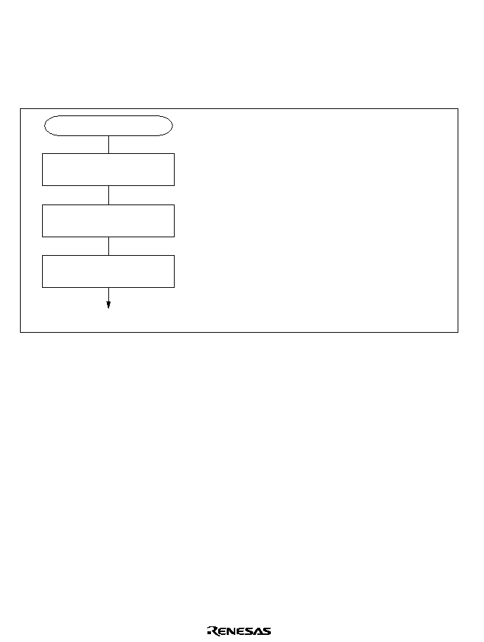
346
Waveform Output by Compare Match: In 16-bit timer channels 0, 1 compare match A or B can
cause the output at the TIOCA or TIOCB pin to go to 0, go to 1, or toggle. In channel 2 the output
can only go to 0 or go to 1.
�
Sample setup procedure for waveform output by compare match
Figure 9.17 shows an example of the setup procedure for waveform output by compare match.
Output setup
Select waveform
output mode
Set output timing
Start counter
Waveform output
Select the compare match output mode (0, 1, or
toggle) in TIOR. When a waveform output mode
is selected, the pin switches from its generic input/
output function to the output compare function
(TIOCA or TIOCB). An output compare pin outputs
the value set in TOLR until the first compare match
occurs.
Set a value in GRA or GRB to designate the
compare match timing.
Set the STR bit in TSTR to 1 to make 16TCNT
start counting.
1
2
3
1.
2.
3.
Figure 9.17 Setup Procedure for Waveform Output by Compare Match (Example)
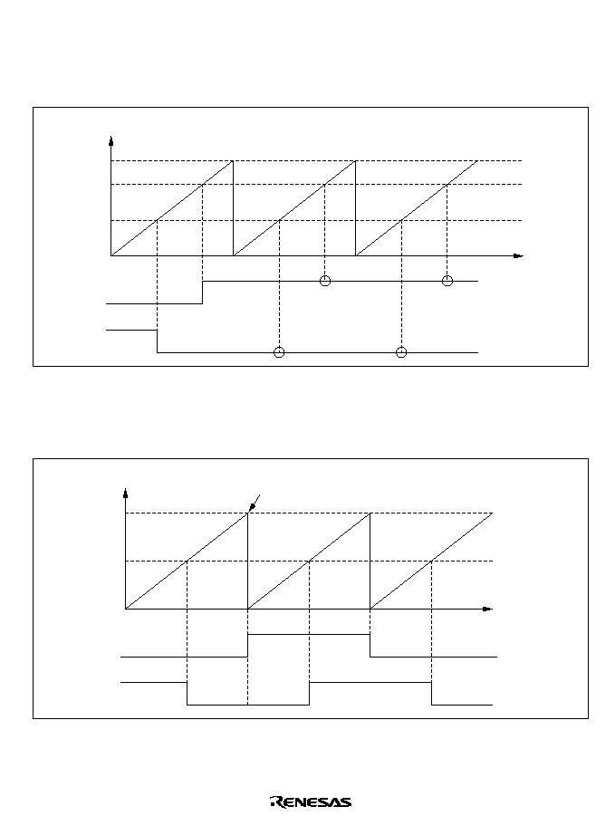
347
�
Examples of waveform output
Figure 9.18 shows examples of 0 and 1 output. 16TCNT operates as a free-running counter, 0
output is selected for compare match A, and 1 output is selected for compare match B. When
the pin is already at the selected output level, the pin level does not change.
Time
H'FFFF
GRB
TIOCB
TIOCA
GRA
No change
No change
No change
No change
1 output
0 output
16TCNT value
H'0000
Figure 9.18 0 and 1 Output (TOA = 1, TOB = 0)
Figure 9.19 shows examples of toggle output. 16TCNT operates as a periodic counter, cleared
by compare match B. Toggle output is selected for both compare match A and B.
GRB
TIOCB
TIOCA
GRA
16TCNT value
Time
Counter cleared by compare match with GRB
Toggle
output
Toggle
output
H'0000
Figure 9.19 Toggle Output (TOA = 1, TOB = 0)
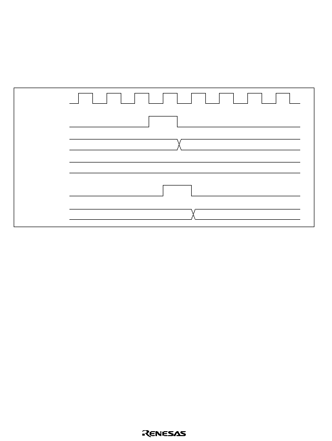
348
�
Output compare output timing
The compare match signal is generated in the last state in which 16TCNT and the general
register match (when 16TCNT changes from the matching value to the next value). When the
compare match signal is generated, the output value selected in TIOR is output at the output
compare pin (TIOCA or TIOCB). When 16TCNT matches a general register, the compare
match signal is not generated until the next counter clock pulse.
Figure 9.20 shows the output compare timing.
N + 1
N
N
16TCNT input
clock
16TCNT
GR
Compare
match signal
TIOCA,
TIOCB
Figure 9.20 Output Compare Output Timing
Input Capture Function: The 16TCNT value can be transferred to a general register when an
input edge is detected at an input capture input/output compare pin (TIOCA or TIOCB). Rising-
edge, falling-edge, or both-edge detection can be selected. The input capture function can be used
to measure pulse width or period.
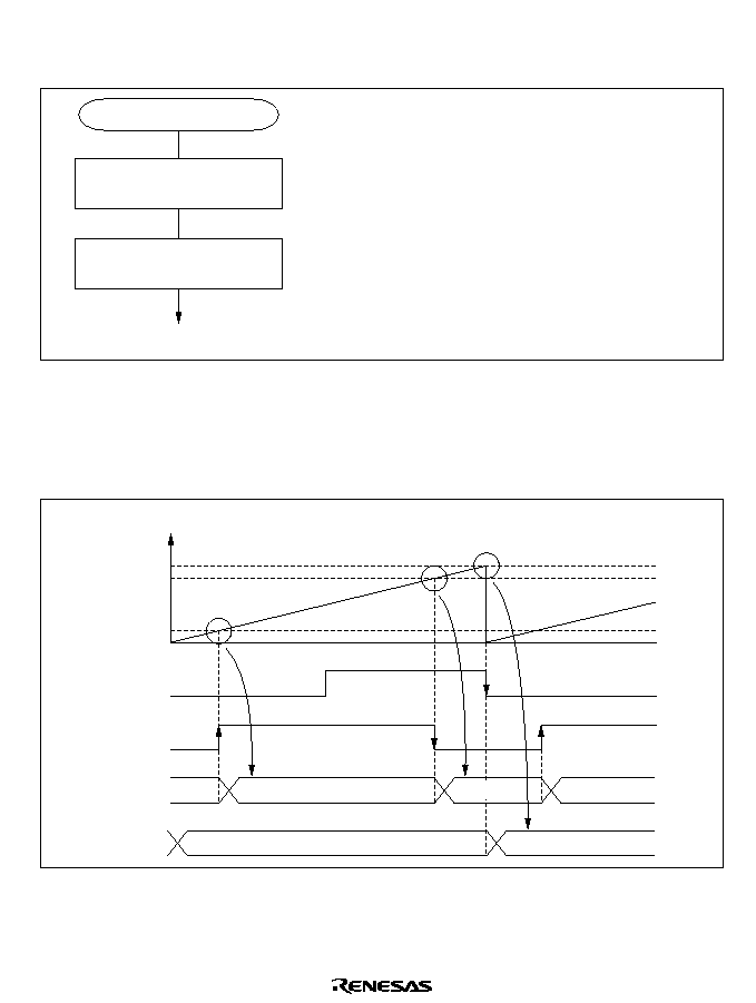
349
�
Sample setup procedure for input capture
Figure 9.21 shows a sample procedure for setting up input capture.
Input selection
Select input-capture input
Start counter
Input capture
Set TIOR to select the input capture function of a
general register and the rising edge, falling edge,
or both edges of the input capture signal. Clear the
DDR bit to 0 before making these TIOR settings.
Set the STR bit in TSTR to 1 to make 16TCNT
start counting.
1
2
1.
2.
Figure 9.21 Setup Procedure for Input Capture (Example)
�
Examples of input capture
Figure 9.22 illustrates input capture when the falling edge of TIOCB and both edges of TIOCA
are selected as capture edges. 16TCNT is cleared by input capture into GRB.
H'0005
H'0180
H'0180
H'0160
H'0005
H'0000
TIOCB
TIOCA
GRA
GRB
16TCNT value
H'0160
Figure 9.22 Input Capture (Example)
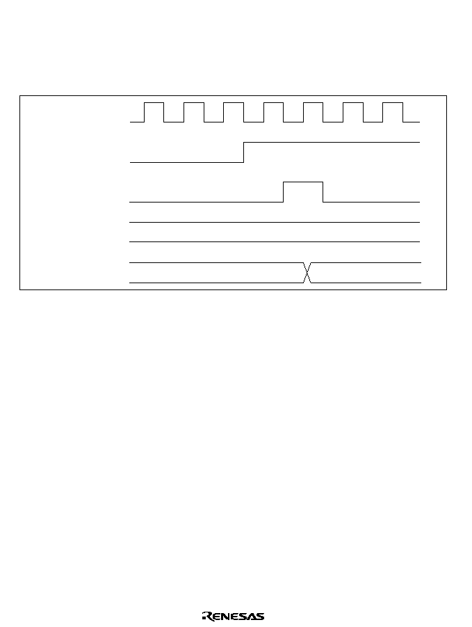
350
�
Input capture signal timing
Input capture on the rising edge, falling edge, or both edges can be selected by settings in
TIOR. Figure 9.23 shows the timing when the rising edge is selected. The pulse width of the
input capture signal must be at least 1.5 system clocks for single-edge capture, and 2.5 system
clocks for capture of both edges.
N
N
Input-capture input
Input capture signal
16TCNT
GRA, GRB
Figure 9.23 Input Capture Signal Timing
9.4.3
Synchronization
The synchronization function enables two or more timer counters to be synchronized by writing
the same data to them simultaneously (synchronous preset). With appropriate 16TCR settings, two
or more timer counters can also be cleared simultaneously (synchronous clear). Synchronization
enables additional general registers to be associated with a single time base. Synchronization can
be selected for all channels (0 to 2).
Sample Setup Procedure for Synchronization: Figure 9.24 shows a sample procedure for
setting up synchronization.
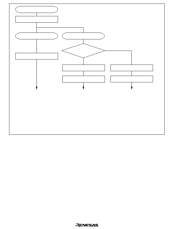
351
Setup for synchronization
Synchronous preset
Set the SYNC bits to 1 in TSNC for the channels to be synchronized.
When a value is written in 16TCNT in one of the synchronized channels, the same value is
simultaneously written in 16TCNT in the other channels.
Set the CCLR1 or CCLR0 bit in 16TCR to have the counter cleared by compare match or input capture.
Set the CCLR1 and CCLR0 bits in 16TCR to have the counter cleared synchronously.
Set the STR bits in TSTR to 1 to start the synchronized counters.
1.
2.
3.
4.
5.
2
3
1
5
4
5
Select synchronization
Synchronous preset
Write to 16TCNT
Synchronous clear
Clearing
synchronized to this
channel?
Select counter clear source
Start counter
Counter clear
Synchronous clear
Start counter
Select counter clear source
Yes
No
Figure 9.24 Setup Procedure for Synchronization (Example)
Example of Synchronization: Figure 9.25 shows an example of synchronization. Channels 0, 1,
and 2 are synchronized, and are set to operate in PWM mode. Channel 0 is set for counter clearing
by compare match with GRB0. Channels 1 and 2 are set for synchronous counter clearing. The
timer counters in channels 0, 1, and 2 are synchronously preset, and are synchronously cleared by
compare match with GRB0. A three-phase PWM waveform is output from pins TIOCA
0
, TIOCA
1
,
and TIOCA
2
. For further information on PWM mode, see section 9.4.4, PWM Mode.
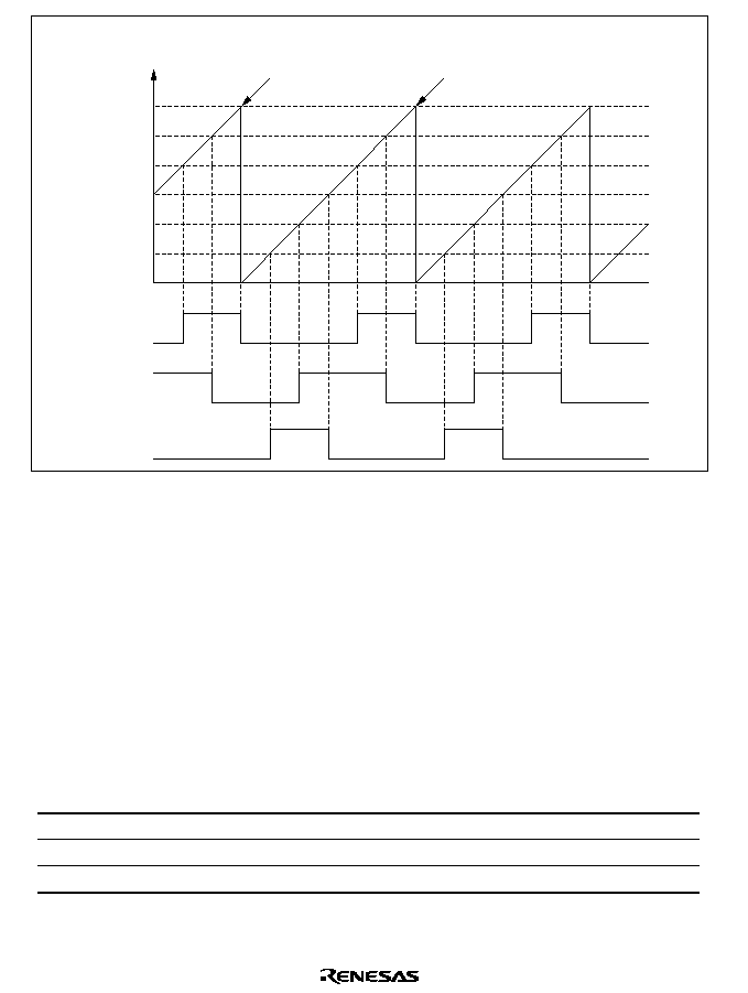
352
TIOCA
2
TIOCA
1
TIOCA
0
GRA2
GRA1
GRB2
GRA0
GRB1
GRB0
Value of 16TCNT0
to 16TCNT2
Cleared by compare match with GRB0
H'0000
Figure 9.25 Synchronization (Example)
9.4.4
PWM Mode
In PWM mode GRA and GRB are paired and a PWM waveform is output from the TIOCA pin.
GRA specifies the time at which the PWM output changes to 1. GRB specifies the time at which
the PWM output changes to 0. If either GRA or GRB compare match is selected as the counter
clear source, a PWM waveform with a duty cycle from 0% to 100% is output at the TIOCA pin.
PWM mode can be selected in all channels (0 to 2).
Table 9.4 summarizes the PWM output pins and corresponding registers. If the same value is set in
GRA and GRB, the output does not change when compare match occurs.
Table 9.4
PWM Output Pins and Registers
Channel
Output Pin
1 Output
0 Output
0
TIOCA
0
GRA0
GRB0
1
TIOCA
1
GRA1
GRB1
2
TIOCA
2
GRA2
GRB2
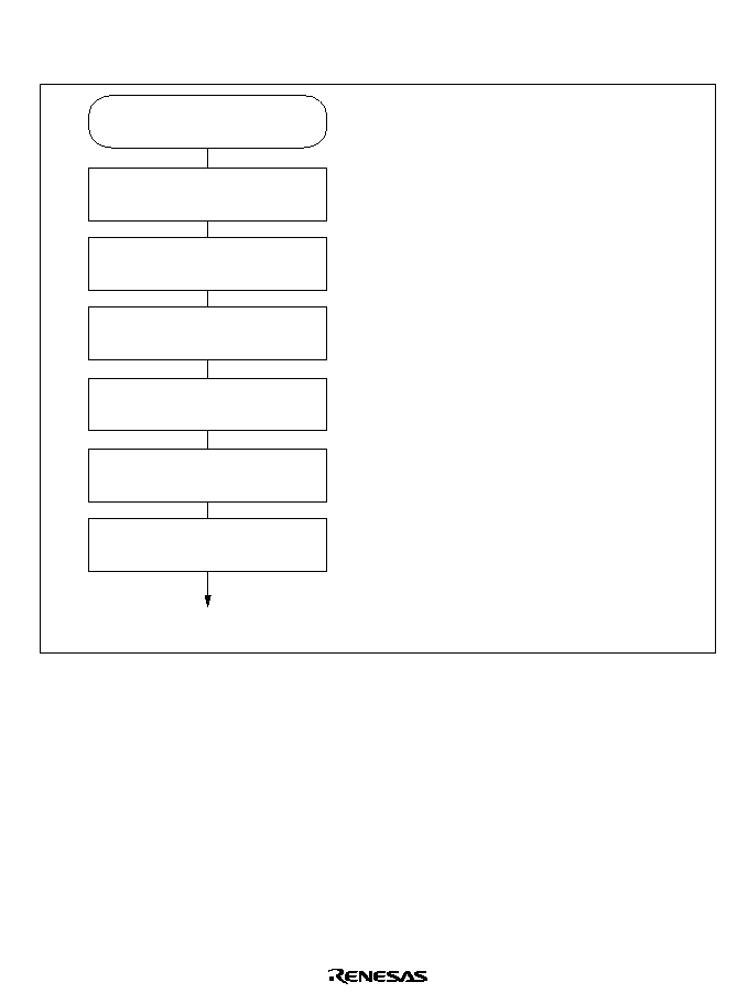
353
Sample Setup Procedure for PWM Mode: Figure 9.26 shows a sample procedure for setting up
PWM mode.
PWM mode
1.
2.
3.
4.
5.
6.
Set bits TPSC2 to TPSC0 in 16TCR to
select the counter clock source. If an
external clock source is selected, set
bits CKEG1 and CKEG0 in 16TCR to
select the desired edge(s) of the
external clock signal.
Set bits CCLR1 and CCLR0 in 16TCR
to select the counter clear source.
Set the time at which the PWM
waveform should go to 1 in GRA.
Set the time at which the PWM
waveform should go to 0 in GRB.
Set the PWM bit in TMDR to select
PWM mode. When PWM mode is
selected, regardless of the TIOR
contents, GRA and GRB become
output compare registers specifying
the times at which the PWM output
goes to 1 and 0. The TIOCA pin
automatically becomes the PWM
output pin. The TIOCB pin conforms
to the settings of bits IOB1 and IOB0
in TIOR. If TIOCB output is not
desired, clear both IOB1 and IOB0 to 0.
Set the STR bit to 1 in TSTR to start
the timer counter.
PWM mode
Select counter clock
1
Select counter clear source
2
Set GRA
3
Set GRB
4
Select PWM mode
5
Start counter
6
Figure 9.26 Setup Procedure for PWM Mode (Example)
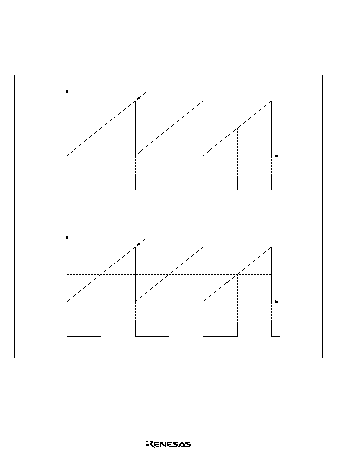
354
Examples of PWM Mode: Figure 9.27 shows examples of operation in PWM mode. In PWM
mode TIOCA becomes an output pin. The output goes to 1 at compare match with GRA, and to 0
at compare match with GRB.
In the examples shown, 16TCNT is cleared by compare match with GRA or GRB. Synchronized
operation and free-running counting are also possible.
16TCNT value
Counter cleared by compare match A
Time
GRA
GRB
TIOCA
a. Counter cleared by GRA (TOA = 1)
16TCNT value
Counter cleared by compare match B
Time
GRB
GRA
TIOCA
b. Counter cleared by GRB (TOA = 0)
H'0000
H'0000
Figure 9.27 PWM Mode (Example 1)
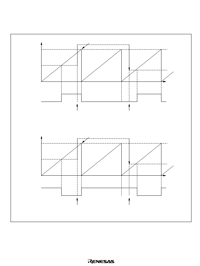
355
Figure 9.28 shows examples of the output of PWM waveforms with duty cycles of 0% and 100%.
If the counter is cleared by compare match with GRB, and GRA is set to a higher value than GRB,
the duty cycle is 0%. If the counter is cleared by compare match with GRA, and GRB is set to a
higher value than GRA, the duty cycle is 100%.
16TCNT value
Counter cleared by compare match B
Time
GRB
GRA
TIOCA
a. 0% duty cycle (TOA=0)
16TCNT value
Counter cleared by compare match A
Time
GRA
GRB
TIOCA
b. 100% duty cycle (TOA=1)
Write to GRA
Write to GRA
Write to GRB
Write to GRB
H'0000
H'0000
Figure 9.28 PWM Mode (Example 2)
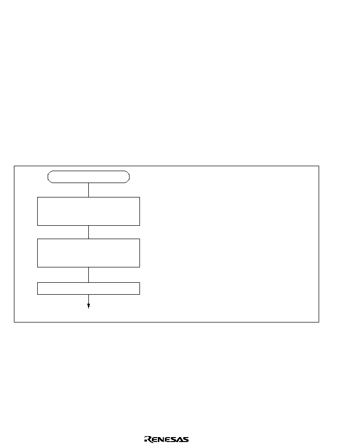
356
9.4.5
Phase Counting Mode
In phase counting mode the phase difference between two external clock inputs (at the TCLKA
and TCLKB pins) is detected, and 16TCNT2 counts up or down accordingly.
In phase counting mode, the TCLKA and TCLKB pins automatically function as external clock
input pins and 16TCNT2 becomes an up/down-counter, regardless of the settings of bits TPSC2 to
TPSC0, CKEG1, and CKEG0 in 16TCR2. Settings of bits CCLR1, CCLR0 in 16TCR2, and
settings in TIOR2, TISRA, TISRB, TISRC, setting of STR2 bit in TSTR, GRA2, and GRB2 are
valid. The input capture and output compare functions can be used, and interrupts can be
generated.
Phase counting is available only in channel 2.
Sample Setup Procedure for Phase Counting Mode: Figure 9.29 shows a sample procedure for
setting up phase counting mode.
Phase counting mode
Select phase counting mode
Select flag setting condition
Start counter
1
2
3
Phase counting mode
1.
2.
3.
Set the MDF bit in TMDR to 1 to select
phase counting mode.
Select the flag setting condition with
the FDIR bit in TMDR.
Set the STR2 bit to 1 in TSTR to start
the timer counter.
Figure 9.29 Setup Procedure for Phase Counting Mode (Example)
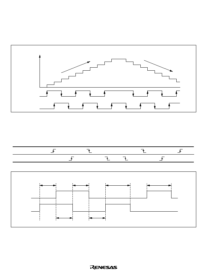
357
Example of Phase Counting Mode: Figure 9.30 shows an example of operations in phase
counting mode. Table 9.5 lists the up-counting and down-counting conditions for 16TCNT2.
In phase counting mode both the rising and falling edges of TCLKA and TCLKB are counted. The
phase difference between TCLKA and TCLKB must be at least 1.5 states, the phase overlap must
also be at least 1.5 states, and the pulse width must be at least 2.5 states.
16TCNT2 value
Counting up
Counting down
TCLKB
TCLKA
Figure 9.30 Operation in Phase Counting Mode (Example)
Table 9.5
Up/Down Counting Conditions
Counting
Direction
Up-Counting
Down-Counting
TCLKB pin
High
Low
HIgh
Low
TCLKA pin
Low
High
Low
HIgh
TCLKA
TCLKB
Phase
difference
Phase
difference
Pulse width
Pulse width
Overlap
Overlap
Phase difference and overlap:
Pulse width:
at least 1.5 states
at least 2.5 states
Figure 9.31 Phase Difference, Overlap, and Pulse Width in Phase Counting Mode
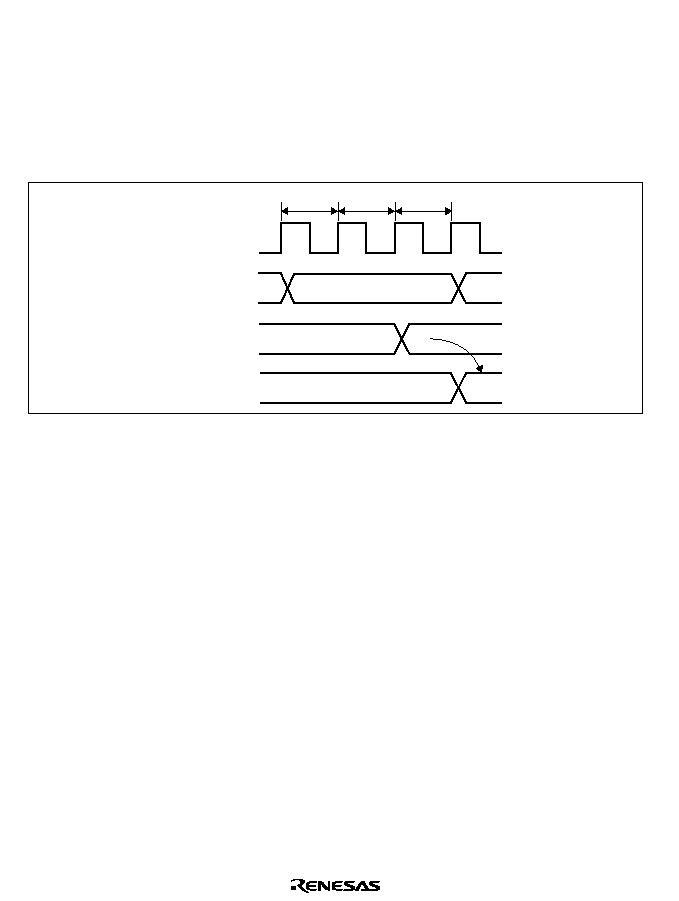
358
9.4.6
16-Bit Timer Output Timing
The initial value of 16-bit timer output when a timer count operation begins can be specified
arbitrarily by making a setting in TOLR.
Figure 9.32 shows the timing for setting the initial value with TOLR.
Only write to TOLR when the corresponding bit in TSTR is cleared to 0.
T
1
TOLR address
N
N
T
2
T
3
Address bus
TOLR
ITU output pin
Figure 9.32 Timing for Setting 16-Bit Timer Output Level by Writing to TOLR
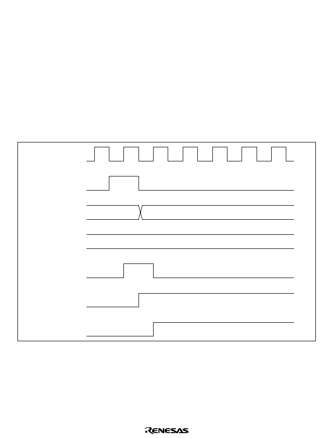
359
9.5
Interrupts
The 16-bit timer has two types of interrupts: input capture/compare match interrupts, and overflow
interrupts.
9.5.1
Setting of Status Flags
Timing of Setting of IMFA and IMFB at Compare Match: IMFA and IMFB are set to 1 by a
compare match signal generated when 16TCNT matches a general register (GR). The compare
match signal is generated in the last state in which the values match (when 16TCNT is updated
from the matching count to the next count). Therefore, when 16TCNT matches a general register,
the compare match signal is not generated until the next 16TCNT clock input. Figure 9.33 shows
the timing of the setting of IMFA and IMFB.
16TCNT
GR
IMF
IMI
16TCNT input
clock
Compare
match signal
N
N + 1
N
Figure 9.33 Timing of Setting of IMFA and IMFB by Compare Match
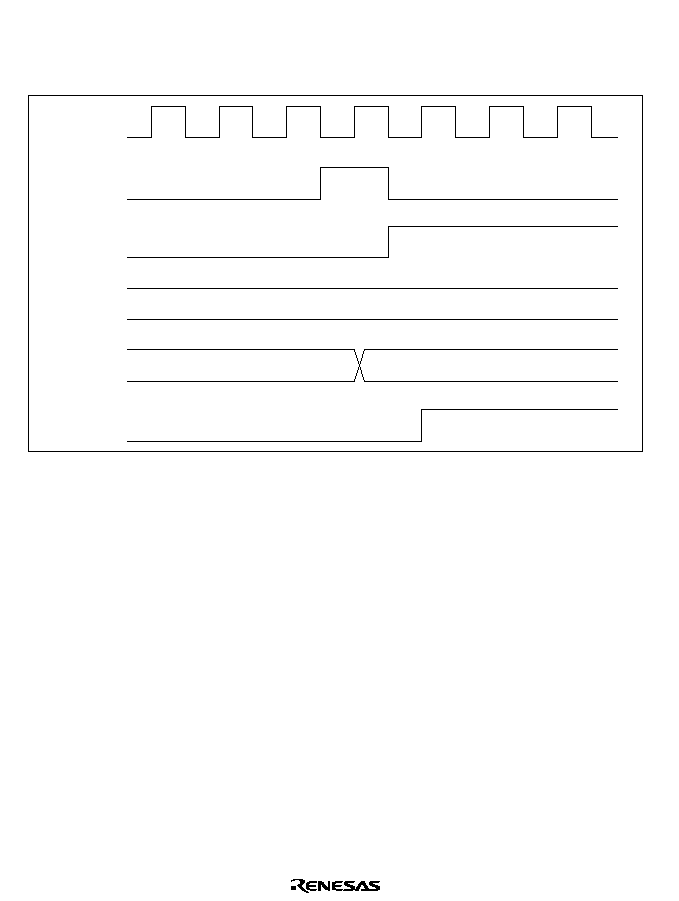
360
Timing of Setting of IMFA and IMFB by Input Capture: IMFA and IMFB are set to 1 by an
input capture signal. The 16TCNT contents are simultaneously transferred to the corresponding
general register. Figure 9.34 shows the timing.
Input capture
signal
N
N
IMF
16TCNT
GR
IMI
Figure 9.34 Timing of Setting of IMFA and IMFB by Input Capture
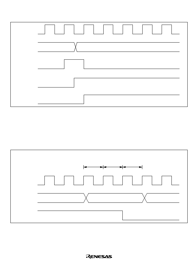
361
Timing of Setting of Overflow Flag (OVF): OVF is set to 1 when 16TCNT overflows from
H'FFFF to H'0000 or underflows from H'0000 to H'FFFF. Figure 9.35 shows the timing.
Overflow
signal
16TCNT
OVF
OVI
Figure 9.35 Timing of Setting of OVF
9.5.2
Timing of Clearing of Status Flags
If the CPU reads a status flag while it is set to 1, then writes 0 in the status flag, the status flag is
cleared. Figure 9.36 shows the timing.
Address
IMF, OVF
TISR write cycle
TISR address
T
1
T
2
T
3
Figure 9.36 Timing of Clearing of Status Flags

362
9.5.3
Interrupt Sources
Each 16-bit timer channel can generate a compare match/input capture A interrupt, a compare
match/input capture B interrupt, and an overflow interrupt. In total there are nine interrupt sources
of three kinds, all independently vectored. An interrupt is requested when the interrupt request flag
are set to 1.
The priority order of the channels can be modified in interrupt priority registers A (IPRA). For
details see section 5, Interrupt Controller.
Table 9.6 lists the interrupt sources.
Table 9.6
16-bit timer Interrupt Sources
Channel
Interrupt
Source
Description
Priority
*
0
IMIA0
IMIB0
OVI0
Compare match/input capture A0
Compare match/input capture B0
Overflow 0
High
1
IMIA1
IMIB1
OVI1
Compare match/input capture A1
Compare match/input capture B1
Overflow 1
2
IMIA2
IMIB2
OVI2
Compare match/input capture A2
Compare match/input capture B2
Overflow 2
Low
Note:
*
The priority immediately after a reset is indicated. Inter-channel priorities can be changed
by settings in IPRA.
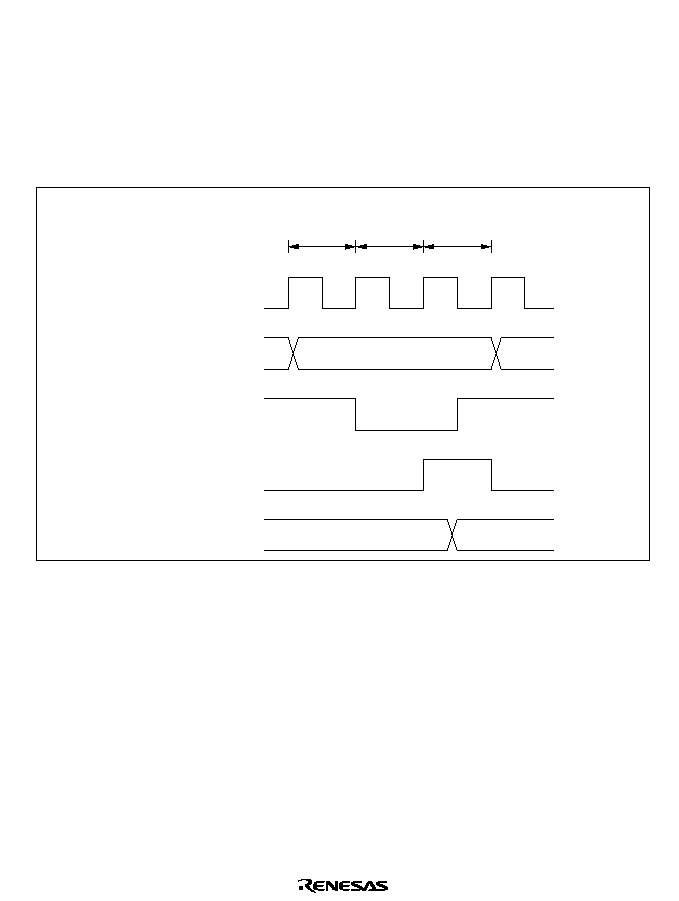
363
9.6
Usage Notes
This section describes contention and other matters requiring special attention during 16-bit timer
operations.
Contention between 16TCNT Write and Clear: If a counter clear signal occurs in the T
3
state of
a 16TCNT write cycle, clearing of the counter takes priority and the write is not performed. See
figure 9.37.
Address bus
Internal write signal
Counter clear signal
16TCNT
16TCNT write cycle
16TCNT address
N
H'0000
T
1
T
2
T
3
Figure 9.37 Contention between 16TCNT Write and Clear
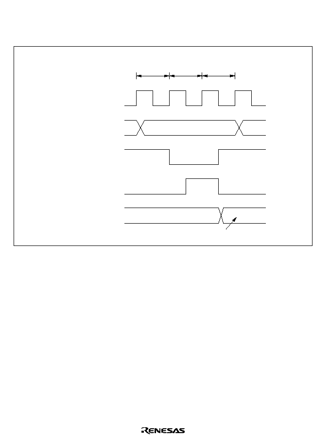
364
Contention between 16TCNT Word Write and Increment: If an increment pulse occurs in the
T
3
state of a 16TCNT word write cycle, writing takes priority and 16TCNT is not incremented.
Figure 9.38 shows the timing in this case.
Address bus
Internal write signal
16TCNT input clock
16TCNT
N
16TCNT address
M
16TCNT write data
16TCNT word write cycle
T
1
T
2
T
3
Figure 9.38 Contention between 16TCNT Word Write and Increment
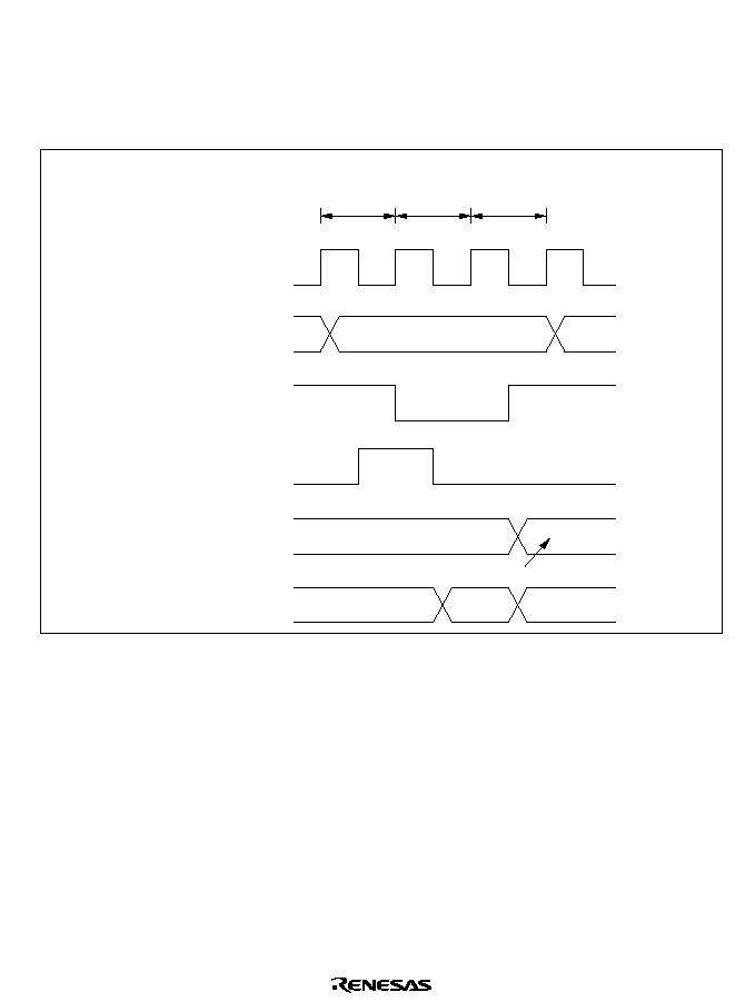
365
Contention between 16TCNT Byte Write and Increment: If an increment pulse occurs in the
T
2
or T
3
state of a 16TCNT byte write cycle, writing takes priority and 16TCNT is not
incremented. The byte data for which a write was not performed is not incremented, and retains its
pre-write value. See figure 9.39, which shows an increment pulse occurring in the T
2
state of a
byte write to 16TCNTH.
Address bus
Internal write signal
16TCNT input clock
16TCNTH
16TCNTL
16TCNTH byte write cycle
T
1
T
2
T
3
N
16TCNTH address
M
16TCNT write data
X
X
X + 1
Figure 9.39 Contention between 16TCNT Byte Write and Increment
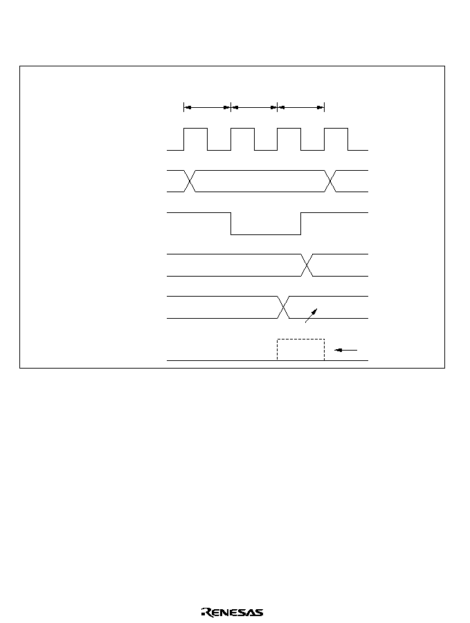
366
Contention between General Register Write and Compare Match: If a compare match occurs
in the T
3
state of a general register write cycle, writing takes priority and the compare match signal
is inhibited. See figure 9.40.
Address bus
Internal write signal
16TCNT
GR
Compare match signal
General register write cycle
T
1
T
2
T
3
N
GR address
M
N
N + 1
General register write data
Inhibited
Figure 9.40 Contention between General Register Write and Compare Match
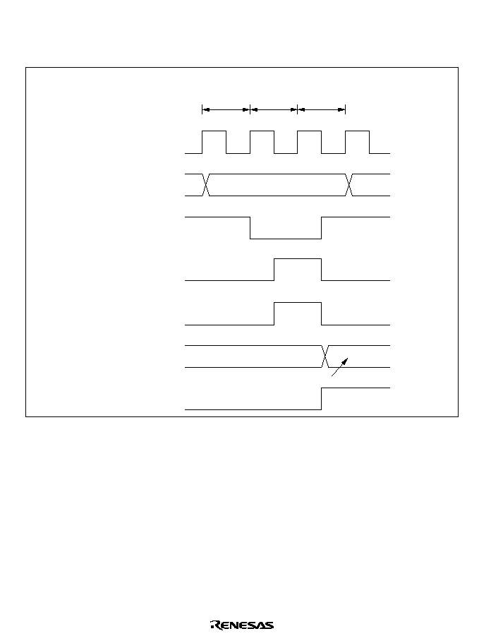
367
Contention between 16TCNT Write and Overflow or Underflow: If an overflow occurs in the
T
3
state of a 16TCNT write cycle, writing takes priority and the counter is not incremented. OVF
is set to 1. The same holds for underflow. See figure 9.41.
Address bus
Internal write signal
16TCNT input clock
Overflow signal
16TCNT
OVF
H'FFFF
16TCNT address
M
16TCNT write data
16TCNT write cycle
T
1
T
2
T
3
Figure 9.41 Contention between 16TCNT Write and Overflow
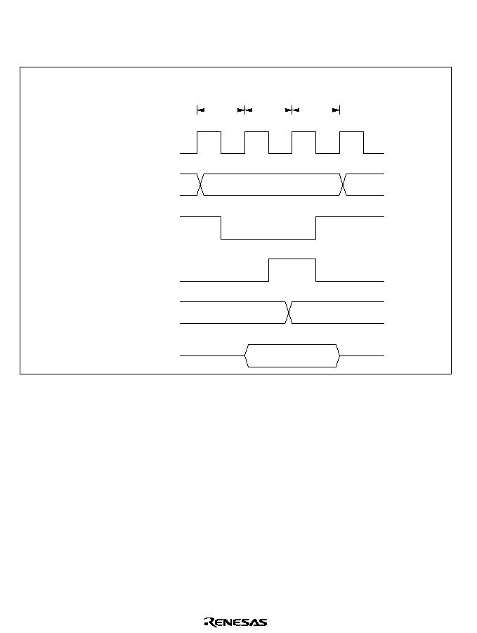
368
Contention between General Register Read and Input Capture: If an input capture signal
occurs during the T
3
state of a general register read cycle, the value before input capture is read.
See figure 9.42.
Address bus
Internal read signal
Input capture signal
GR
Internal data bus
GR address
X
General register read cycle
T
1
T
2
T
3
X
M
Figure 9.42 Contention between General Register Read and Input Capture
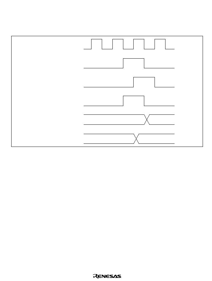
369
Contention between Counter Clearing by Input Capture and Counter Increment: If an input
capture signal and counter increment signal occur simultaneously, the counter is cleared according
to the input capture signal. The counter is not incremented by the increment signal. The value
before the counter is cleared is transferred to the general register. See figure 9.43.
Input capture signal
Counter clear signal
16TCNT input clock
16TCNT
GR
N
N
H'0000
Figure 9.43 Contention between Counter Clearing by Input Capture and Counter
Increment
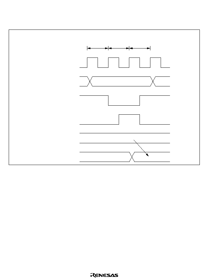
370
Contention between General Register Write and Input Capture: If an input capture signal
occurs in the T
3
state of a general register write cycle, input capture takes priority and the write to
the general register is not performed. See figure 9.44.
Address bus
Internal write signal
Input capture signal
16TCNT
GR
M
GR address
General register write cycle
T
1
T
2
T
3
M
Figure 9.44 Contention between General Register Write and Input Capture
371
Note on Waveform Period Setting: When a counter is cleared by compare match, the counter is
cleared in the last state at which the 16TCNT value matches the general register value, at the time
when this value would normally be updated to the next count. The actual counter frequency is
therefore given by the following formula:
f =
(N+1)
(f: counter frequency.
: system clock frequency. N: value set in general register.)
Note on Writes in Synchronized Operation: When channels are synchronized, if a 16TCNT
value is modified by byte write access, all 16 bits of all synchronized counters assume the same
value as the counter that was addressed.
(Example) When channels 1 and 2 are synchronized
� Byte write to channel 1 or byte write to channel 2
16TCNT1
16TCNT2
W
Y
X
Z
16TCNT1
16TCNT2
A
A
X
X
16TCNT1
16TCNT2
Y
Y
A
A
16TCNT1
16TCNT2
W
Y
X
Z
16TCNT1
16TCNT2
A
A
B
B
� Word write to channel 1 or word write to channel 2
Upper byte Lower byte
Upper byte Lower byte
Upper byte Lower byte
Upper byte Lower byte
Upper byte Lower byte
Write A to upper byte
of channel 1
Write A to lower byte
of channel 2
Write AB word to
channel 1 or 2
372
16-bit timer Operating Modes
Table 9.7 (a) 16-bit timer Operating Modes (Channel 0)
Register Settings
TSNC
TMDR
TIOR0
16TCR0
Synchro-
Clear Clock
Operating Mode
nization
MDF
FDIR PWM
IOA
IOB
Select
Select
Synchronous preset
SYNC0 = 1 --
--
PWM mode
--
--
PWM0 = 1
--
*
Output compare A
--
--
PWM0 = 0
IOA2 = 0
Other bits
unrestricted
Output compare B
--
--
IOB2 = 0
Other bits
unrestricted
Input capture A
--
--
PWM0 = 0
IOA2 = 1
Other bits
unrestricted
Input capture B
--
--
PWM0 = 0
IOB2 = 1
Other bits
unrestricted
Counter By compare
--
--
CCLR1 = 0
clearing match/input
CCLR0 = 1
capture A
By compare
--
--
CCLR1 = 1
match/input
CCLR0 = 0
capture B
Syn-
SYNC0 = 1 --
--
CCLR1 = 1
chronous
CCLR0 = 1
clear
Legend:
Setting available (valid). -- Setting does not affect this mode.
Note:
*
The input capture function cannot be used in PWM mode. If compare match A and compare match B occur
simultaneously, the compare match signal is inhibited.
373
Table 9.7 (b) 16-bit timer Operating Modes (Channel 1)
Register Settings
TSNC
TMDR
TIOR1
16TCR1
Synchro-
Clear Clock
Operating Mode
nization
MDF
FDIR PWM
IOA
IOB
Select
Select
Synchronous preset
SYNC1 = 1 --
--
PWM mode
--
--
PWM1 = 1
--
Output compare A
--
--
PWM1 = 0
IOA2 = 0
Other bits
unrestricted
Output compare B
--
--
IOB2 = 0
Other bits
unrestricted
Input capture A
--
--
PWM1 = 0
IOA2 = 1
Other bits
unrestricted
Input capture B
--
--
PWM1 = 0
IOB2 = 1
Other bits
unrestricted
Counter By compare
--
--
CCLR1 = 0
clearing match/input
CCLR0 = 1
capture A
By compare
--
--
CCLR1 = 1
match/input
CCLR0 = 0
capture B
Syn-
SYNC1 = 1 --
--
CCLR1 = 1
chronous
CCLR0 = 1
clear
Legend:
Setting available (valid). -- Setting does not affect this mode.
Note:
The input capture function cannot be used in PWM mode. If compare match A and compare match B
occur simultaneously, the compare match signal is inhibited.
*
*
374
Table 9.7 (c) 16-bit timer Operating Modes (Channel 2)
Register Settings
TSNC
TMDR
TIOR2
16TCR2
Synchro-
Clear Clock
Operating Mode
nization
MDF
FDIR PWM
IOA
IOB
Select
Select
Synchronous preset
SYNC2 = 1
--
PWM mode
--
PWM2 = 1
--
*
Output compare A
--
PWM2 = 0
IOA2 = 0
Other bits
unrestricted
Output compare B
--
IOB2 = 0
Other bits
unrestricted
Input capture A
--
PWM2 = 0
IOA2 = 1
Other bits
unrestricted
Input capture B
--
PWM2 = 0
IOB2 = 1
Other bits
unrestricted
Counter By compare
--
CCLR1 = 0
clearing match/input
CCLR0 = 1
capture A
By compare
--
CCLR1 = 1
match/input
CCLR0 = 0
capture B
Syn-
SYNC2 = 1
--
CCLR1 = 1
chronous
CCLR0 = 1
clear
Phase counting
MDF = 1
--
mode
Legend:
Setting available (valid). -- Setting does not affect this mode.
Note:
*
The input capture function cannot be used in PWM mode. If compare match A and compare match B occur
simultaneously, the compare match signal is inhibited.

375
Section 10 8-Bit Timers
10.1
Overview
The H8/3069F has a built-in 8-bit timer module with four channels (TMR0, TMR1, TMR2, and
TMR3), based on 8-bit counters. Each channel has an 8-bit timer counter (8TCNT) and two 8-bit
time constant registers (TCORA and TCORB) that are constantly compared with the 8TCNT
value to detect compare match events. The timers can be used as multifunctional timers in a
variety of applications, including the generation of a rectangular-wave output with an arbitrary
duty cycle.
10.1.1
Features
The features of the 8-bit timer module are listed below.
�
Selection of four clock sources
The counters can be driven by one of three internal clock signals (
/8,
/64, or
/8192) or an
external clock input (enabling use as an external event counter).
�
Selection of three ways to clear the counters
The counters can be cleared on compare match A or B, or input capture B.
�
Timer output controlled by two compare match signals
The timer output signal in each channel is controlled by two independent compare match
signals, enabling the timer to generate output waveforms with an arbitrary duty cycle or PWM
output.
�
A/D converter can be activated by a compare match
�
Two channels can be cascaded
Channels 0 and 1 can be operated as the upper and lower halves of a 16-bit timer (16-bit
count mode).
Channels 2 and 3 can be operated as the upper and lower halves of a 16-bit timer (16-bit
count mode).
Channel 1 can count channel 0 compare match events (compare match count mode).
Channel 3 can count channel 2 compare match events (compare match count mode).
�
Input capture function can be set
8-bit or 16-bit input capture operation is available.

376
�
Twelve interrupt sources
There are twelve interrupt sources: four compare match sources, four compare match/input
capture sources, four overflow sources.
Two of the compare match sources and two of the combined compare match/input capture
sources each have an independent interrupt vector. The remaining compare match interrupts,
combined compare match/input capture interrupts, and overflow interrupts have one interrupt
vector for two sources.
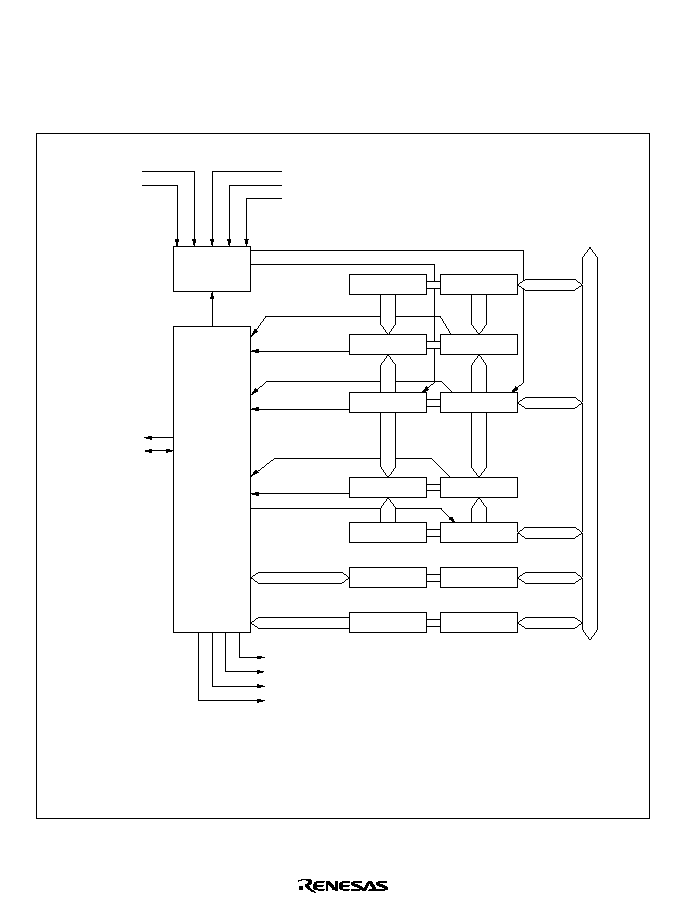
377
10.1.2
Block Diagram
The 8-bit timers are divided into two groups of two channels each: group 0 comprising channels 0
and 1, and group 1 comprising channels 2 and 3. Figure 10.1 shows a block diagram of 8-bit timer
group 0.
/8
/64
/8192
CMIA0
CMIB0
CMIA1/CMIB1
OVI0/OVI1
Interrupt signals
TMO
0
TMIO
1
TCORA0
TCORB0
8TCSR0
8TCR0
TCORA1
8TCNT1
TCORB1
8TCSR1
8TCR1
TCLKA
TCLKC
8TCNT0
Legend:
TCORA: Time constant register A
TCORB: Time constant register B
8TCNT: Timer
counter
8TCSR: Timer control/status register
8TCR:
Timer control register
External clock
sources
Internal clock
sources
Clock select
Control logic
Clock 1
Clock 0
Compare match A1
Compare match A0
Overflow 1
Overflow 0
Compare match B1
Compare match B0
Input capture B1
Comparator A0
Comparator A1
Comparator B0
Comparator B1
Internal bus
Figure 10.1 Block Diagram of 8-Bit Timer Unit (Two Channels: Group 0)

378
10.1.3
Pin Configuration
Table 10.1 summarizes the input/output pins of the 8-bit timer module.
Table 10.1
8-Bit Timer Pins
Group
Channel Name
Abbreviation I/O
Function
0
0
Timer output
TMO
0
Output Compare match output
Timer clock input
TCLKC
Input
Counter external clock input
1
Timer input/output TMIO
1
I/O
Compare match output/input
capture input
Timer clock input
TCLKA
Input
Counter external clock input
1
2
Timer output
TMO
2
Output Compare match output
Timer clock input
TCLKD
Input
Counter external clock input
3
Timer input/output TMIO
3
I/O
Compare match output/input
capture input
Timer clock input
TCLKB
Input
Counter external clock input

379
10.1.4
Register Configuration
Table 10.2 summarizes the registers of the 8-bit timer module.
Table 10.2
8-Bit Timer Registers
Channel
Address
*
1
Name
Abbreviation R/W
Initial value
0
H'FFF80
Timer control register 0
8TCR0
R/W
H'00
H'FFF82
Timer control/status register 0
8TCSR0
R/(W)
*
2
H'00
H'FFF84
Time constant register A0
TCORA0
R/W
H'FF
H'FFF86
Time constant register B0
TCORB0
R/W
H'FF
H'FFF88
Timer counter 0
8TCNT0
R/W
H'00
1
H'FFF81
Timer control register 1
8TCR1
R/W
H'00
H'FFF83
Timer control/status register 1
8TCSR1
R/(W)
*
2
H'00
H'FFF85
Time constant register A1
TCORA1
R/W
H'FF
H'FFF87
Time constant register B1
TCORB1
R/W
H'FF
H'FFF89
Timer counter 1
8TCNT1
R/W
H'00
2
H'FFF90
Timer control register 2
8TCR2
R/W
H'00
H'FFF92
Timer control/status register 2
8TCSR2
R/(W)
*
2
H'10
H'FFF94
Time constant register A2
TCORA2
R/W
H'FF
H'FFF96
Time constant register B2
TCORB2
R/W
H'FF
H'FFF98
Timer counter 2
8TCNT2
R/W
H'00
3
H'FFF91
Timer control register 3
8TCR3
R/W
H'00
H'FFF93
Timer control/status register 3
8TCSR3
R/(W)
*
2
H'00
H'FFF95
Time constant register A3
TCORA3
R/W
H'FF
H'FFF97
Time constant register B3
TCORB3
R/W
H'FF
H'FFF99
Timer counter 3
8TCNT3
R/W
H'00
Notes:
*
1 Indicates the lower 20 bits of the address in advanced mode.
*
2 Only 0 can be written to bits 7 to 5, to clear these flags.
Each pair of registers for channel 0 and channel 1 comprises a 16-bit register with the channel 0
register as the upper 8 bits and the channel 1 register as the lower 8 bits, so they can be accessed
together by word access.
Similarly, each pair of registers for channel 2 and channel 3 comprises a 16-bit register with the
channel 2 register as the upper 8 bits and the channel 3 register as the lower 8 bits, so they can be
accessed together by word access.
380
10.2
Register Descriptions
10.2.1
Timer Counters (8TCNT)
15
0
R/W
Bit
Initial value
Read/Write
14
0
R/W
Bit
Initial value
Read/Write
13
0
R/W
12
0
R/W
11
0
R/W
10
0
R/W
9
0
R/W
8
0
R/W
7
0
R/W
6
0
R/W
5
0
R/W
4
0
R/W
3
0
R/W
2
0
R/W
1
0
R/W
0
0
R/W
8TCNT0
8TCNT1
15
0
R/W
14
0
R/W
13
0
R/W
12
0
R/W
11
0
R/W
10
0
R/W
9
0
R/W
8
0
R/W
7
0
R/W
6
0
R/W
5
0
R/W
4
0
R/W
3
0
R/W
2
0
R/W
1
0
R/W
0
0
R/W
8TCNT2
8TCNT3
The timer counters (8TCNT) are 8-bit readable/writable up-counters that increment on pulses
generated from an internal or external clock source. The clock source is selected by clock select
bits 2 to 0 (CKS2 to CKS0) in the timer control register (8TCR). The CPU can always read or
write to the timer counters.
The 8TCNT0 and 8TCNT1 pair, and the 8TCNT2 and 8TCNT3 pair, can each be accessed as a
16-bit register by word access.
8TCNT can be cleared by an input capture signal or compare match signal. Counter clear bits 1
and 0 (CCLR1 and CCLR0) in 8TCR select the method of clearing.
When 8TCNT overflows from H'FF to H'00, the overflow flag (OVF) in the timer control/status
register (8TCSR) is set to 1.
Each 8TCNT is initialized to H'00 by a reset and in standby mode.
381
10.2.2
Time Constant Registers A (TCORA)
TCORA0 to TCORA3 are 8-bit readable/writable registers.
15
1
R/W
14
1
R/W
13
1
R/W
12
1
R/W
11
1
R/W
10
1
R/W
9
1
R/W
8
1
R/W
7
1
R/W
6
1
R/W
5
1
R/W
4
1
R/W
3
1
R/W
2
1
R/W
1
1
R/W
0
1
R/W
TCORA0
TCORA1
15
1
R/W
14
1
R/W
13
1
R/W
12
1
R/W
11
1
R/W
10
1
R/W
9
1
R/W
8
1
R/W
7
1
R/W
6
1
R/W
5
1
R/W
4
1
R/W
3
1
R/W
2
1
R/W
1
1
R/W
0
1
R/W
TCORA2
TCORA3
Bit
Initial value
Read/Write
Bit
Initial value
Read/Write
The TCORA0 and TCORA1 pair, and the TCORA2 and TCORA3 pair, can each be accessed as a
16-bit register by word access.
The TCORA value is constantly compared with the 8TCNT value. When a match is detected, the
corresponding compare match flag A (CMFA) is set to 1 in 8TCSR.
The timer output can be freely controlled by these compare match signals and the settings of
output select bits 1 and 0 (OS1, OS0) in 8TCSR.
Each TCORA register is initialized to H'FF by a reset and in standby mode.
382
10.2.3
Time Constant Registers B (TCORB)
15
1
R/W
14
1
R/W
13
1
R/W
12
1
R/W
11
1
R/W
10
1
R/W
9
1
R/W
8
1
R/W
7
1
R/W
6
1
R/W
5
1
R/W
4
1
R/W
3
1
R/W
2
1
R/W
1
1
R/W
0
1
R/W
TCORB0
TCORB1
15
1
R/W
14
1
R/W
13
1
R/W
12
1
R/W
11
1
R/W
10
1
R/W
9
1
R/W
8
1
R/W
7
1
R/W
6
1
R/W
5
1
R/W
4
1
R/W
3
1
R/W
2
1
R/W
1
1
R/W
0
1
R/W
TCORB2
TCORB3
Bit
Initial value
Read/Write
Bit
Initial value
Read/Write
TCORB0 to TCORB3 are 8-bit readable/writable registers. The TCORB0 and TCORB1 pair, and
the TCORB2 and TCORB3 pair, can each be accessed as a 16-bit register by word access.
The TCORB value is constantly compared with the 8TCNT value. When a match is detected, the
corresponding compare match flag B (CMFB) is set to 1 in 8TCSR*.
The timer output can be freely controlled by these compare match signals and the settings of
output/input capture edge select bits 3 and 2 (OIS3, OIS2) in 8TCSR.
When TCORB is used for input capture, it stores the 8TCNT value on detection of an external
input capture signal. At this time, the CMFB flag is set to 1 in the corresponding 8TCSR register.
The detected edge of the input capture signal is set in 8TCSR.
Each TCORB register is initialized to H'FF by a reset and in standby mode.
Note: * When channel 1 and channel 3 are designated for TCORB input capture, the CMFB flag is
not set by a channel 0 or channel 2 compare match B.

383
10.2.4
Timer Control Register (8TCR)
7
CMIEB
0
R/W
6
CMIEA
0
R/W
5
OVIE
0
R/W
4
CCLR1
0
R/W
3
CCLR0
0
R/W
0
CKS0
0
R/W
2
CKS2
0
R/W
1
CKS1
0
R/W
Bit
Initial value
Read/Write
8TCR is an 8-bit readable/writable register that selects the 8TCNT input clock, gives the 8TCNT
clearing specification, and enables interrupt requests.
8TCR is initialized to H'00 by a reset and in standby mode.
For the timing, see section 10.4, Operation.
Bit 7--Compare Match Interrupt Enable B (CMIEB): Enables or disables the CMIB interrupt
request when the CMFB flag is set to 1 in 8TCSR.
Bit 7
CMIEB
Description
0
CMIB interrupt requested by CMFB is disabled
(Initial value)
1
CMIB interrupt requested by CMFB is enabled
Bit 6--Compare Match Interrupt Enable A (CMIEA): Enables or disables the CMIA interrupt
request when the CMFA flag is set to 1 in 8TCSR.
Bit 6
CMIEA
Description
0
CMIA interrupt requested by CMFA is disabled
(Initial value)
1
CMIA interrupt requested by CMFA is enabled
Bit 5--Timer Overflow Interrupt Enable (OVIE): Enables or disables the OVI interrupt request
when the OVF flag is set to 1 in 8TCSR.
Bit 5
OVIE
Description
0
OVI interrupt requested by OVF is disabled
(Initial value)
1
OVI interrupt requested by OVF is enabled

384
Bits 4 and 3--Counter Clear 1 and 0 (CCLR1, CCLR0): These bits specify the 8TCNT
clearing source. Compare match A or B, or input capture B, can be selected as the clearing source.
Bit 4
CCLR1
Bit 3
CCLR0
Description
0
0
Clearing is disabled
(Initial value)
1
Cleared by compare match A
1
0
Cleared by compare match B/input capture B
1
Cleared by input capture B
Note:
When input capture B is set as the 8TCNT1 and 8TCNT3 counter clear source, 8TCNT0
and 8TCNT2 are not cleared by compare match B.
Bits 2 to 0--Clock Select 2 to 0 (CSK2 to CSK0): These bits select whether the clock input to
8TCNT is an internal or external clock.
Three internal clocks can be selected, all divided from the system clock (
):
/8,
/64, and
/8192.
The rising edge of the selected internal clock triggers the count.
When use of an external clock is selected, three types of count can be selected: at the rising edge,
the falling edge, and both rising and falling edges.
When CKS2, CKS1, CKS0 = 1, 0, 0, channels 0 and 1 and channels 2 and 3 are cascaded.
The incrementing clock source is different when 8TCR0 and 8TCR2 are set, and when 8TCR1 and
8TCR3 are set.

385
Bit 2
CSK2
Bit 1
CSK1
Bit 0
CSK0
Description
0
0
0
Clock input disabled
(Initial value)
1
Internal clock, counted on falling edge of
/8
1
0
Internal clock, counted on falling edge of
/64
1
Internal clock, counted on falling edge of
/8192
1
0
0
Channel 0 (16-bit count mode): Count on 8TCNT1 overflow
signal
*
1
Channel 1 (compare match count mode): Count on 8TCNT0
compare match A
*
1
Channel 2 (16-bit count mode): Count on 8TCNT3 overflow
signal
*
2
Channel 3 (compare match count mode): Count on 8TCNT2
compare match A
*
2
1
External clock, counted on rising edge
1
0
External clock, counted on falling edge
1
External clock, counted on both rising and falling edges
Notes:
*
1 If the clock input of channel 0 is the 8TCNT1 overflow signal and that of channel 1 is the
8TCNT0 compare match signal, no incrementing clock is generated. Do not use this
setting.
*
2 If the clock input of channel 2 is the 8TCNT3 overflow signal and that of channel 3 is the
8TCNT2 compare match signal, no incrementing clock is generated. Do not use this
setting.
386
10.2.5
Timer Control/Status Registers (8TCSR)
7
CMFB
0
R/(W)
*
6
CMFA
0
R/(W)
*
5
OVF
0
R/(W)
*
4
--
1
--
3
OIS3
0
R/W
0
OS0
0
R/W
2
OIS2
0
R/W
1
OS1
0
R/W
8TCSR2
7
CMFB
0
R/(W)
*
6
CMFA
0
R/(W)
*
5
OVF
0
R/(W)
*
4
0
R/W
3
OIS3
0
R/W
0
OS0
0
R/W
2
OIS2
0
R/W
1
OS1
0
R/W
8TCSR0
ADTE
Bit
Initial value
Read/Write
Bit
Initial value
Read/Write
7
CMFB
0
R/(W)
*
6
CMFA
0
R/(W)
*
5
OVF
0
R/(W)
*
4
ICE
0
R/W
3
OIS3
0
R/W
0
OS0
0
R/W
2
OIS2
0
R/W
1
OS1
0
R/W
8TCSR1, 8TCSR3
Note:
*
Only 0 can be written to bits 7 to 5, to clear these flags.
Bit
Initial value
Read/Write
The timer control/status registers 8TCSR are 8-bit registers that indicate compare match/input
capture and overflow statuses, and control compare match output/input capture edge selection.
8TCSR2 is initialized to H'10, and 8TCSR0, 8TCSR1, and 8TCSR3 to H'00, by a reset and in
standby mode.

387
Bit 7--Compare Match/Input Capture Flag B (CMFB): Status flag that indicates the
occurrence of a TCORB compare match or input capture.
Bit 7
CMFB
Description
0
[Clearing condition]
(Initial value)
Read CMFB when CMFB = 1, then write 0 in CMFB
1
[Setting conditions]
�
8TCNT = TCORB
*
�
The 8TCNT value is transferred to TCORB by an input capture signal when
TCORB functions as an input capture register
Note:
*
When bit ICE is set to 1 in 8TCSR1 and 8TCSR3, the CMFB flag is not set when 8TCNT0 =
TCORB0 or 8TCNT2 = TCORB2.
Bit 6--Compare Match Flag A (CMFA): Status flag that indicates the occurrence of a TCORA
compare match.
Bit 6
CMFA
Description
0
[Clearing condition]
(Initial value)
Read CMFA when CMFA = 1, then write 0 in CMFA
1
[Setting condition]
8TCNT = TCORA
Bit 5--Timer Overflow Flag (OVF): Status flag that indicates that the 8TCNT has overflowed
from H'FF to H'00.
Bit 5
OVF
Description
0
[Clearing condition]
(Initial value)
Read OVF when OVF = 1, then write 0 in OVF
1
[Setting condition]
8TCNT overflows from H'FF to H'00

388
Bit 4--A/D Trigger Enable (ADTE) (In 8TCSR0): In combination with TRGE in the A/D
control register (ADCR), enables or disables A/D converter start requests by compare match A or
an external trigger.
TRGE
*
Bit 4
ADTE
Description
0
0
A/D converter start requests by compare match A or external trigger pin
(
ADTRG
) input are disabled
(Initial value)
1
A/D converter start requests by compare match A or external trigger pin
(
ADTRG
) input are disabled
1
0
A/D converter start requests by external trigger pin (
ADTRG
) input are
enabled, and A/D converter start requests by compare match A are disabled
1
A/D converter start requests by compare match A are enabled, and A/D
converter start requests by external trigger pin (
ADTRG
) input are disabled
Note:
*
TRGE is bit 7 of the A/D control register (ADCR).
Bit 4--Reserved (In 8TCSR1): This bit is a reserved bit, but can be read and written.
Bit 4--Input Capture Enable (ICE) (In 8TCSR1 and 8TCSR3): Selects the function of
TCORB1 and TCORB3.
Bit 4
ICE
Description
0
TCORB1 and TCORB3 are compare match registers
(Initial value)
1
TCORB1 and TCORB3 are input capture registers
When bit ICE is set to 1 in 8TCSR1 or 8TCSR3, the operation of the TCORA and TCORB
registers in channels 0 to 3 is as shown in the tables below.

389
Table 10.3
Operation of Channels 0 and 1 when Bit ICE is Set to 1 in 8TCSR1 Register
Register
Register
Function
Status Flag Change
Timer Output
Capture Input
Interrupt Request
TCORA0 Compare match
operation
CMFA changed from 0
to 1 in 8TCSR0 by
compare match
TMO
0
output
controllable
CMIA0 interrupt request
generated by compare
match
TCORB0 Compare match
operation
CMFB not changed
from 0 to 1 in 8TCSR0
by compare match
No output from
TMO
0
CMIB0 interrupt request
not generated by compare
match
TCORA1 Compare match
operation
CMFA changed from 0
to 1 in 8TCSR1 by
compare match
TMIO
1
is dedicated
input capture pin
CMIA1 interrupt request
generated by compare
match
TCORB1 Input capture
operation
CMFB changed from 0
to 1 in 8TCSR1 by
input capture
TMIO
1
is dedicated
input capture pin
CMIB1 interrupt request
generated by input
capture
Table 10.4
Operation of Channels 2 and 3 when Bit ICE is Set to 1 in 8TCSR3 Register
Register
Register
Function
Status Flag Change
Timer Output
Capture Input
Interrupt Request
TCORA2 Compare match
operation
CMFA changed from 0
to 1 in 8TCSR2 by
compare match
TMO
2
output
controllable
CMIA2 interrupt request
generated by compare
match
TCORB2 Compare match
operation
CMFB not changed
from 0 to 1 in 8TCSR2
by compare match
No output from
TMO
2
CMIB2 interrupt request
not generated by compare
match
TCORA3 Compare match
operation
CMFA changed from 0
to 1 in 8TCSR3 by
compare match
TMIO
3
is dedicated
input capture pin
CMIA3 interrupt request
generated by compare
match
TCORB3 Input capture
operation
CMFB changed from 0
to 1 in 8TCSR3 by
input capture
TMIO
3
is dedicated
input capture pin
CMIB3 interrupt request
generated by input
capture

390
Bits 3 and 2--Output/Input Capture Edge Select B3 and B2 (OIS3, OIS2): In combination
with the ICE bit in 8TCSR1 (8TCSR3), these bits select the compare match B output level or the
input capture input detected edge.
The function of TCORB1 (TCORB3) depends on the setting of bit 4 of 8TCSR1 (8TCSR3).
ICE Bit in
8TCSR1
(8TCSR3)
Bit 3
OIS3
Bit 2
OIS2
Description
0
0
0
No change when compare match B occurs
(Initial value)
1
0 is output when compare match B occurs
1
0
1 is output when compare match B occurs
1
Output is inverted when compare match B occurs (toggle output)
1
0
0
TCORB input capture on rising edge
1
TCORB input capture on falling edge
1
0
TCORB input capture on both rising and falling edges
1
�
When the compare match register function is used, the timer output priority order is: toggle
output > 1 output > 0 output.
�
If compare match A and B occur simultaneously, the output changes in accordance with the
higher-priority compare match.
�
When bits OIS3, OIS2, OS1, and OS0 are all cleared to 0, timer output is disabled.
Bits 1 and 0--Output Select A1 and A0 (OS1, OS0): These bits select the compare match A
output level.
Bit 1
OS1
Bit 0
OS0
Description
0
0
No change when compare match A occurs
(Initial value)
1
0 is output when compare match A occurs
1
0
1 is output when compare match A occurs
1
Output is inverted when compare match A occurs (toggle output)
�
When the compare match register function is used, the timer output priority order is: toggle
output > 1 output > 0 output.
�
If compare match A and B occur simultaneously, the output changes in accordance with the
higher-priority compare match.
�
When bits OIS3, OIS2, OS1, and OS0 are all cleared to 0, timer output is disabled.
391
10.3
CPU Interface
10.3.1
8-Bit Registers
8TCNT, TCORA, TCORB, 8TCR, and 8TCSR are 8-bit registers. These registers are connected
to the CPU by an internal 16-bit data bus and can be read and written a word at a time or a byte at
a time.
Figures 10.2 and 10.3 show the operation in word read and write accesses to 8TCNT.
Figures 10.4 to 10.7 show the operation in byte read and write accesses to 8TCNT0 and 8TCNT1.
8TCNT0 8TCNT1
H
L
H
L
C
P
U
Internal data bus
Bus
interface
Module data bus
Figure 10.2 8TCNT Access Operation (CPU Writes to 8TCNT, Word)
8TCNT0 8TCNT1
H
L
H
L
C
P
U
Internal data bus
Bus
interface
Module data bus
Figure 10.3 8TCNT Access Operation (CPU Reads 8TCNT, Word)
8TCNTH0 8TCNTL1
H
L
H
L
C
P
U
Internal data bus
Bus
interface
Module data bus
Figure 10.4 8TCNT0 Access Operation (CPU Writes to 8TCNT0, Upper Byte)
392
8TCNTH0 8TCNTL1
H
L
H
L
C
P
U
Internal data bus
Bus
interface
Module data bus
Figure 10.5 8TCNT1 Access Operation (CPU Writes to 8TCNT1, Lower Byte)
8TCNT0
8TCNT1
H
L
H
L
C
P
U
Internal data bus
Bus
interface
Module data bus
Figure 10.6 8TCNT0 Access Operation (CPU Reads 8TCNT0, Upper Byte)
8TCNT0 8TCNT1
H
L
H
L
C
P
U
Internal data bus
Bus
interface
Module data bus
Figure 10.7 8TCNT1 Access Operation (CPU Reads 8TCNT1, Lower Byte)
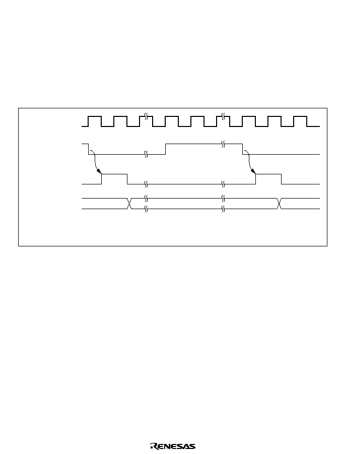
393
10.4
Operation
10.4.1
8TCNT Count Timing
8TCNT is incremented by input clock pulses (either internal or external).
Internal Clock: Three different internal clock signals (
/8,
/64, or
/8192) divided from the
system clock (
) can be selected, by setting bits CKS2 to CKS0 in 8TCR. Figure 10.8 shows the
count timing.
8TCNT
N�1
N
N+1
Internal clock
8TCNT input clock
Note: Even if the same internal clock is selected for the 16-bit timer and the 8-bit timer, the same operation
will not be performed since the incrementing edge is different in each case.
Figure 10.8 Count Timing for Internal Clock Input
External Clock: Three incrementation methods can be selected by setting bits CKS2 to CKS0 in
8TCR: on the rising edge, the falling edge, and both rising and falling edges.
The pulse width of the external clock signal must be at least 1.5 system clocks when a single edge
is selected, and at least 2.5 system clocks when both edges are selected. Shorter pulses will not be
counted correctly.
Figure 10.9 shows the timing for incrementation on both edges of the external clock signal.
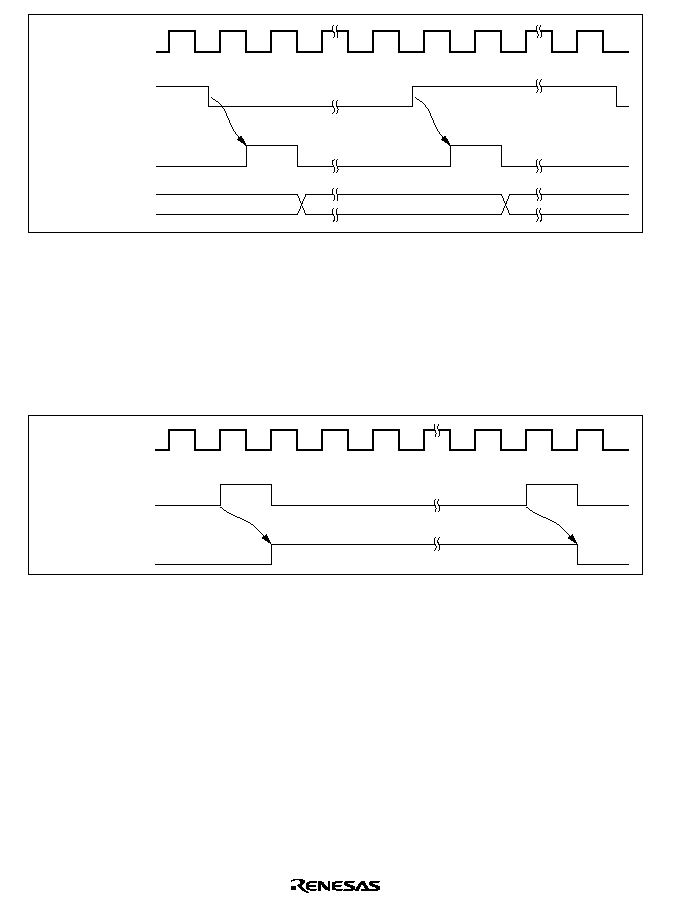
394
8TCNT
N�1
N
N+1
External clock input
8TCNT input clock
Figure 10.9 Count Timing for External Clock Input (Both-Edge Detection)
10.4.2
Compare Match Timing
Timer Output Timing: When compare match A or B occurs, the timer output is as specified by
the OIS3, OIS2, OS1, and OS0 bits in 8TCSR (unchanged, 0 output, 1 output, or toggle output).
Figure 10.10 shows the timing when the output is set to toggle on compare match A.
Compare match A
signal
Timer output
Figure 10.10 Timing of Timer Output
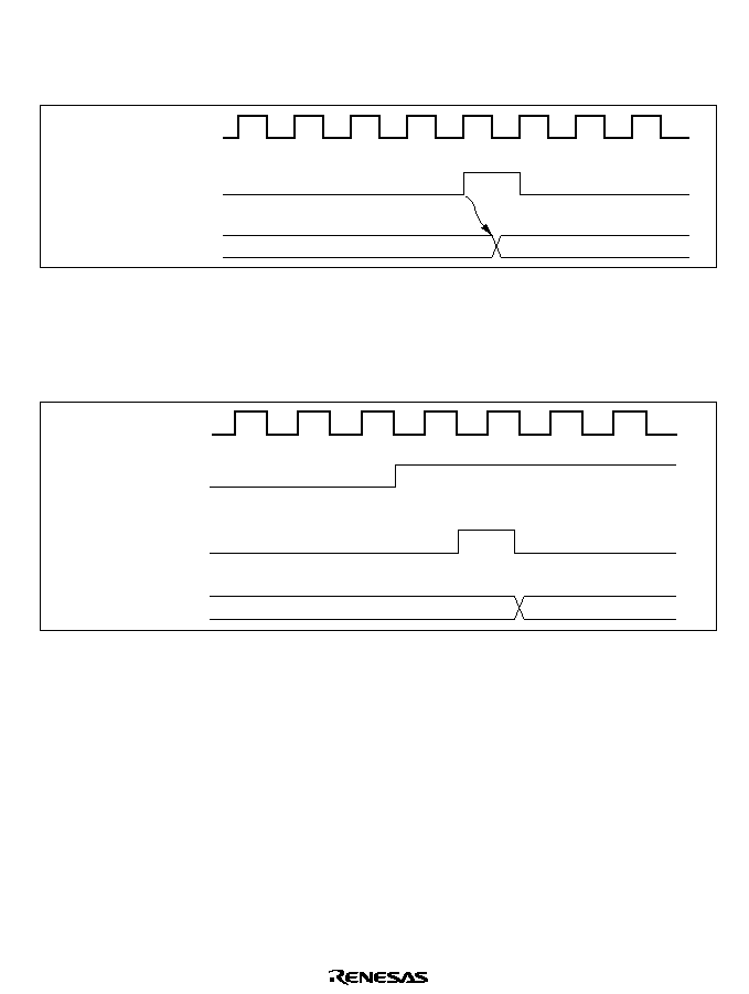
395
Clear by Compare Match: Depending on the setting of the CCLR1 and CCLR0 bits in 8TCR,
8TCNT can be cleared when compare match A or B occurs, Figure 10.11 shows the timing of
this operation.
N
H'00
8TCNT
Compare match signal
Figure 10.11 Timing of Clear by Compare Match
Clear by Input Capture: Depending on the setting of the CCLR1 and CCLR0 bits in 8TCR,
8TCNT can be cleared when input capture B occurs. Figure 10.12 shows the timing of this
operation.
Input capture signal
Input capture input
8TCNT
N
H '00
Figure 10.12 Timing of Clear by Input Capture
10.4.3
Input Capture Signal Timing
Input capture on the rising edge, falling edge, or both edges can be selected by settings in 8TCSR.
Figure 10.13 shows the timing when the rising edge is selected.
The pulse width of the input capture input signal must be at least 1.5 system clocks when a single
edge is selected, and at least 2.5 system clocks when both edges are selected.
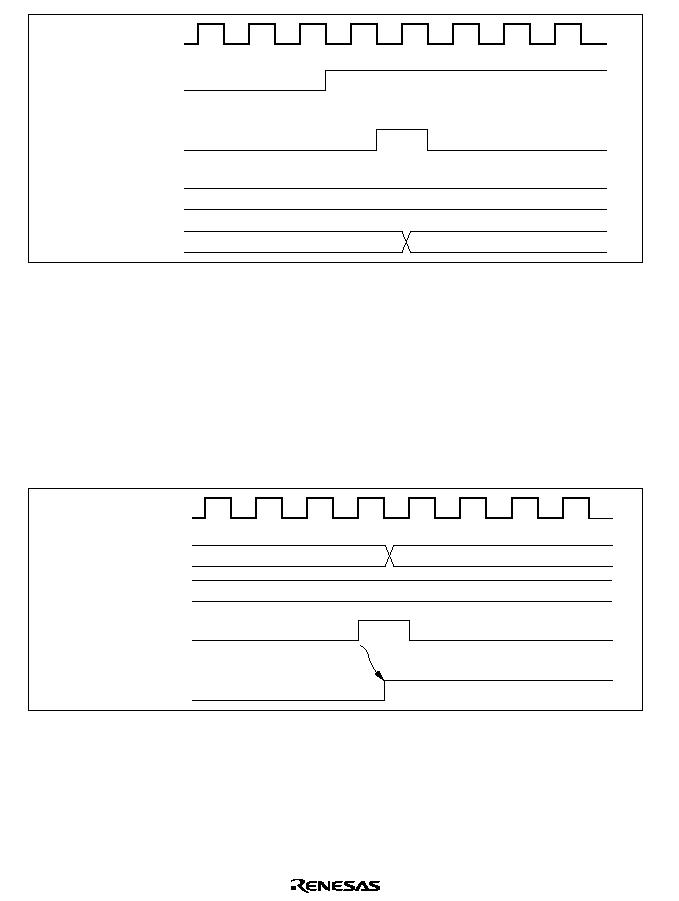
396
Input capture signal
Input capture input
8TCNT
N
TCORB
N
Figure 10.13 Timing of Input Capture Input Signal
10.4.4
Timing of Status Flag Setting
Timing of CMFA/CMFB Flag Setting when Compare Match Occurs: The CMFA and CMFB
flags in 8TCSR are set to 1 by the compare match signal output when the TCORA or TCORB and
8TCNT values match. The compare match signal is generated in the last state of the match (when
the matched 8TCNT count value is updated). Therefore, after the 8TCNT and TCORA or
TCORB values match, the compare match signal is not generated until an incrementing clock
pulse signal is generated. Figure 10.14 shows the timing in this case.
CMF
Compare match signal
8TCNT
N
N+1
N
TCOR
Figure 10.14 CMF Flag Setting Timing when Compare Match Occurs
Timing of CMFB Flag Setting when Input Capture Occurs: On generation of an input capture
signal, the CMFB flag is set to 1 and at the same time the 8TCNT value is transferred to TCORB.
Figure 10.15 shows the timing in this case.
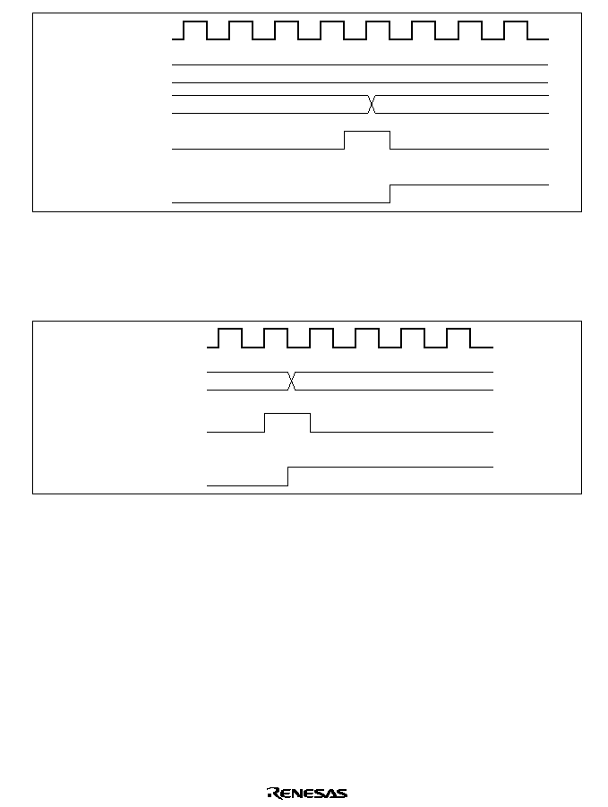
397
CMFB
Input capture signal
8TCNT
N
N
TCORB
Figure 10.15 CMFB Flag Setting Timing when Input Capture Occurs
Timing of Overflow Flag (OVF) Setting: The OVF flag in 8TCSR is set to 1 by the overflow
signal generated when 8TCNT overflows (from H'FF to H'00). Figure 10.16 shows the timing in
this case.
OVF
Overflow signal
8TCNT
H'FF
H'00
Figure 10.16 Timing of OVF Setting
10.4.5
Operation with Cascaded Connection
If bits CKS2 to CKS0 are set to (100) in either 8TCR0 or 8TCR1, the 8-bit timers of channels 0
and 1 are cascaded. With this configuration, the two timers can be used as a single 16-bit timer
(16-bit timer mode), or channel 0 8-bit timer compare matches can be counted in channel 1
(compare match count mode). Similarly, if bits CKS2 to CKS0 are set to (100) in either 8TCR2 or
8TCR3, the 8-bit timers of channels 2 and 3 are cascaded. With this configuration, the two timers
can be used as a single 16-bit timer (16-bit timer mode),or channel 2 8-bit timer compare matches
can be counted in channel 3 (compare match count mode). In this case, the timer operates as
below.

398
16-Bit Count Mode
�
Channels 0 and 1:
When bits CKS2 to CKS0 are set to (100) in 8TCR0, the timer functions as a single 16-bit
timer with channel 0 occupying the upper 8 bits and channel 1 occupying the lower 8 bits.
Setting when Compare Match Occurs
�
The CMFA or CMFB flag is set to 1 in 8TCSR0 when a 16-bit compare match occurs.
�
The CMFA or CMFB flag is set to 1 in 8TCSR1 when a lower 8-bit compare match
occurs.
�
TMO
0
pin output control by bits OIS3, OIS2, OS1, and OS0 in 8TCSR0 is in
accordance with the 16-bit compare match conditions.
�
TMIO
1
pin output control by bits OIS3, OIS2, OS1, and OS0 in 8TCSR1 is in
accordance with the lower 8-bit compare match conditions.
Setting when Input Capture Occurs
�
The CMFB flag is set to 1 in 8TCSR0 and 8TCSR1 when the ICE bit is 1 in TCSR1
and input capture occurs.
�
TMIO
1
pin input capture input signal edge detection is selected by bits OIS3 and OIS2
in 8TCSR0.
Counter Clear Specification
�
If counter clear on compare match or input capture has been selected by the CCLR1 and
CCLR0 bits in 8TCR0, the 16-bit counter (both 8TCNT0 and 8TCNT1) is cleared.
�
The settings of the CCLR1 and CCLR0 bits in 8TCR1 are ignored. The lower 8 bits
cannot be cleared independently.
OVF Flag Operation
�
The OVF flag is set to 1 in 8TCSR0 when the 16-bit counter (8TCNT0 and 8TCNT1)
overflows (from H'FFFF to H'0000).
�
The OVF flag is set to 1 in 8TCSR1 when the 8-bit counter (8TCNT1) overflows (from
H'FF to H'00).
�
Channels 2 and 3:
When bits CKS2 to CKS0 are set to (100) in 8TCR2, the timer functions as a single 16-bit
timer with channel 2 occupying the upper 8 bits and channel 3 occupying the lower 8 bits.
Setting when Compare Match Occurs
�
The CMFA or CMFB flag is set to 1 in 8TCSR2 when a 16-bit compare match occurs.
�
The CMFA or CMFB flag is set to 1 in 8TCSR3 when a lower 8-bit compare match
occurs.
�
TMO
2
pin output control by bits OIS3, OIS2, OS1, and OS0 in 8TCSR2 is in
accordance with the 16-bit compare match conditions.
�
TMIO
3
pin output control by bits OIS3, OIS2, OS1, and OS0 in 8TCSR3 is in
accordance with the lower 8-bit compare match conditions.

399
Setting when Input Capture Occurs
�
The CMFB flag is set to 1 in 8TCSR2 and 8TCSR3 when the ICE bit is 1 in TCSR3
and input capture occurs.
�
TMIO
3
pin input capture input signal edge detection is selected by bits OIS3 and OIS2
in 8TCSR2.
Counter Clear Specification
�
If counter clear on compare match has been selected by the CCLR1 and CCLR0 bits in
8TCR2, the 16-bit counter (both 8TCNT2 and 8TCNT3) is cleared.
�
The settings of the CCLR1 and CCLR0 bits in 8TCR3 are ignored. The lower 8 bits
cannot be cleared independently.
OVF Flag Operation
�
The OVF flag is set to 1 in 8TCSR2 when the 16-bit counter (8TCNT2 and 8TCNT3)
overflows (from H'FFFF to H'0000).
�
The OVF flag is set to 1 in 8TCSR3 when the 8-bit counter (8TCNT3) overflows (from
H'FF to H'00).
Compare Match Count Mode
�
Channels 0 and 1:
When bits CKS2 to CKS0 are set to (100) in 8TCR1, 8TCNT1 counts channel 0 compare
match A events.
CMF flag setting, interrupt generation, TMO pin output, counter clearing, and so on, is in
accordance with the settings for each channel.
Note:
When bit ICE = 1 in 8TCSR1, the compare match register function of TCORB0 in
channel 0 cannot be used.
�
Channels 2 and 3:
When bits CKS2 to CKS0 are set to (100) in 8TCR3, 8TCNT3 counts channel 2 compare
match A events.
CMF flag setting, interrupt generation, TMO pin output, counter clearing, and so on, is in
accordance with the settings for each channel.
Caution
Do not set 16-bit counter mode and compare match count mode simultaneously within the same
group, as the 8TCNT input clock will not be generated and the counters will not operate.

400
10.4.6
Input Capture Setting
The 8TCNT value can be transferred to TCORB on detection of an input edge on the input
capture/output compare pin (TMIO
1
or TMIO
3
). Rising edge, falling edge, or both edge detection
can be selected. In 16-bit count mode, 16-bit input capture can be used.
Setting Input Capture Operation in 8-Bit Timer Mode (Normal Operation)
�
Channel 1:
Set TCORB1 as an 8-bit input capture register with the ICE bit in 8TCSR1.
Select rising edge, falling edge, or both edges as the input edge(s) for the input capture
signal (TMIO
1
) with bits OIS3 and OIS2 in 8TCSR1.
Select the input clock with bits CKS2 to CKS0 in 8TCR1, and start the 8TCNT count.
�
Channel 3:
Set TCORB3 as an 8-bit input capture register with the ICE bit in 8TCSR3.
Select rising edge, falling edge, or both edges as the input edge(s) for the input capture
signal (TMIO
3
) with bits OIS3 and OIS2 in 8TCSR3.
Select the input clock with bits CKS2 to CKS0 in 8TCR3, and start the 8TCNT count.
Note:
When TCORB1 in channel 1 is used for input capture, TCORB0 in channel 0 cannot be
used as a compare match register.
Similarly, when TCORB3 in channel 3 is used for input capture, TCORB2 in channel 2
cannot be used as a compare match register.
Setting Input Capture Operation in 16-Bit Count Mode
�
Channels 0 and 1:
In 16-bit count mode, TCORB0 and TCORB1 function as a 16-bit input capture register
when the ICE bit is set to 1 in 8TCSR1.
Select rising edge, falling edge, or both edges as the input edge(s) for the input capture
signal (TMIO
1
) with bits OIS3 and OIS2 in 8TCSR0. (In 16-bit count mode, the settings of
bits OIS3 and OIS2 in 8TCSR1 are ignored.)
Select the input clock with bits CKS2 to CKS0 in 8TCR1, and start the 8TCNT count.
�
Channels 2 and 3:
In 16-bit count mode, TCORB2 and TCORB3 function as a 16-bit input capture register
when the ICE bit is set to 1 in 8TCSR3.
Select rising edge, falling edge, or both edges as the input edge(s) for the input capture
signal (TMIO
3
) with bits OIS3 and OIS2 in 8TCSR2. (In 16-bit count mode, the settings of
bits OIS3 and OIS2 in 8TCSR3 are ignored.)
Select the input clock with bits CKS2 to CKS0 in 8TCR3, and start the 8TCNT count.

401
10.5
Interrupt
10.5.1
Interrupt Sources
The 8-bit timer unit can generate three types of interrupt: compare match A and B (CMIA and
CMIB) and overflow (TOVI). Table 10.5 shows the interrupt sources and their priority order.
Each interrupt source is enabled or disabled by the corresponding interrupt enable bit in 8TCR. A
separate interrupt request signal is sent to the interrupt controller by each interrupt source.
Table 10.5
Types of 8-Bit Timer Interrupt Sources and Priority Order
Priority
Interrupt Source
Description
High
CMIA
Interrupt by CMFA
CMIB
Interrupt by CMFB
TOVI
Interrupt by OVF
Low
For compare match interrupts (CMIA1/CMIB1 and CMIA3/CMIB3) and the overflow interrupts
(TOVI0/TOVI1 and TOVI2/TOVI3),
one vector is shared by two interrupts.
Table 10.6 lists the interrupt sources.
Table 10.6
8-Bit Timer Interrupt Sources
Channel
Interrupt Source
Description
0
CMIA0
TCORA0 compare match
CMIB0
TCORB0 compare match/input capture
1
CMIA1/CMIB1
TCORA1 compare match, or TCORB1 compare match/input
capture
0, 1
TOVI0/TOVI1
Counter 0 or counter 1 overflow
2
CMIA2
TCORA2 compare match
CMIB2
TCORB2 compare match/input capture
3
CMIA3/CMIB3
TCORA3 compare match, or TCORB3 compare match/input
capture
2, 3
TOVI2/TOVI3
Counter 2 or counter 3 overflow
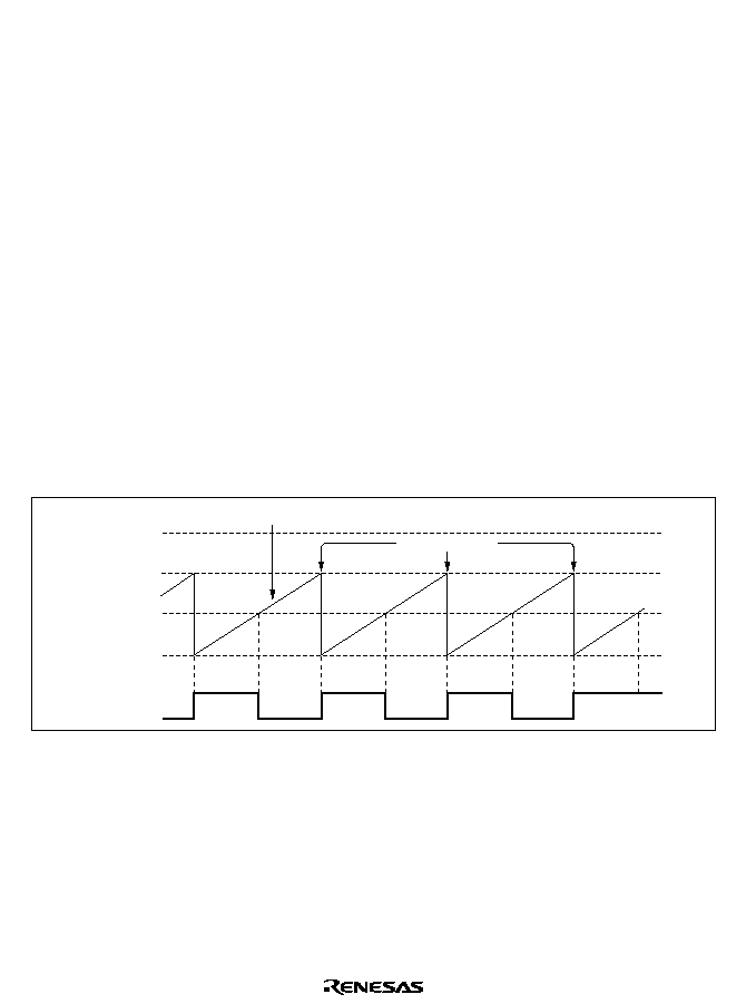
402
10.5.2
A/D Converter Activation
The A/D converter can only be activated by channel 0 compare match A.
If the ADTE bit setting is 1 when the CMFA flag in 8TCSR0 is set to 1 by generation of channel 0
compare match A, an A/D conversion start request will be issued to the A/D converter. If the
TRGE bit in ADCR is 1 at this time, the A/D converter will be started. If the ADTE bit in
8TCSR0 is 1, A/D converter external trigger pin (
ADTRG) input is disabled.
10.6
8-Bit Timer Application Example
Figure 10.17 shows how the 8-bit timer module can be used to output pulses with any desired duty
cycle. The settings for this example are as follows:
�
Clear the CCLR1 bit to 0 and set the CCLR0 bit to 1 in 8TCR so that 8TCNT is cleared by a
TCORA compare match.
�
Set bits OIS3, OIS2, OS1, and OS0 to (0110) in 8TCSR so that 1 is output on a TCORA
compare match and 0 is output on a TCORB compare match.
The above settings enable a waveform with the cycle determined by TCORA and the pulse width
detected by TCORB to be output without software intervention.
8TCNT
H'FF
Counter clear
TCORA
TCORB
H'00
TMO
Figure 10.17 Example of Pulse Output
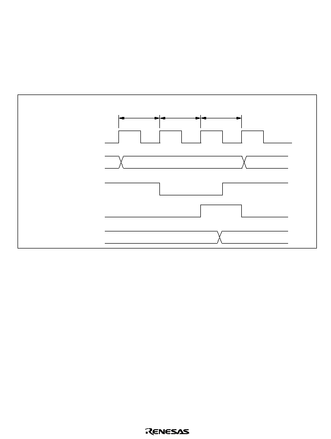
403
10.7
Usage Notes
Note that the following kinds of contention can occur in 8-bit timer operation.
10.7.1
Contention between 8TCNT Write and Clear
If a timer counter clear signal occurs in the T
3
state of a 8TCNT write cycle, clearing of the
counter takes priority and the write is not performed. Figure 10.18 shows the timing in this case.
Address bus
8TCNT address
Internal write signal
Counter clear signal
8TCNT
N
H'00
T
1
T
3
T
2
8TCNT write cycle
Figure 10.18 Contention between 8TCNT Write and Clear
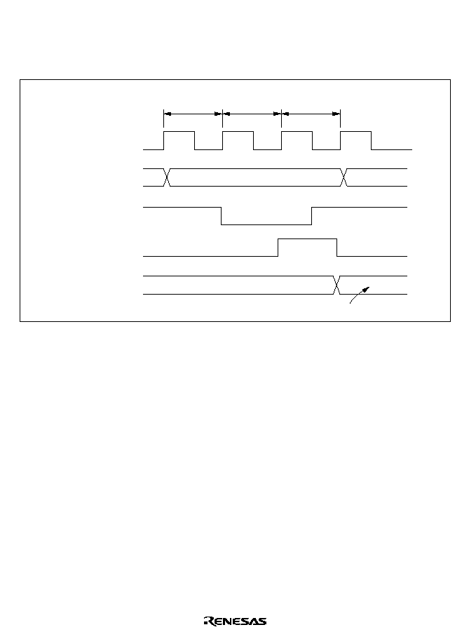
404
10.7.2
Contention between 8TCNT Write and Increment
If an increment pulse occurs in the T
3
state of a 8TCNT write cycle, writing takes priority and
8TCNT is not incremented. Figure 10.19 shows the timing in this case.
Address bus
8 TCNT address
Internal write signal
8TCNT input clock
8TCNT
N
M
T
1
T
3
T
2
8TCNT write cycle
8TCNT write data
Figure 10.19 Contention between 8TCNT Write and Increment
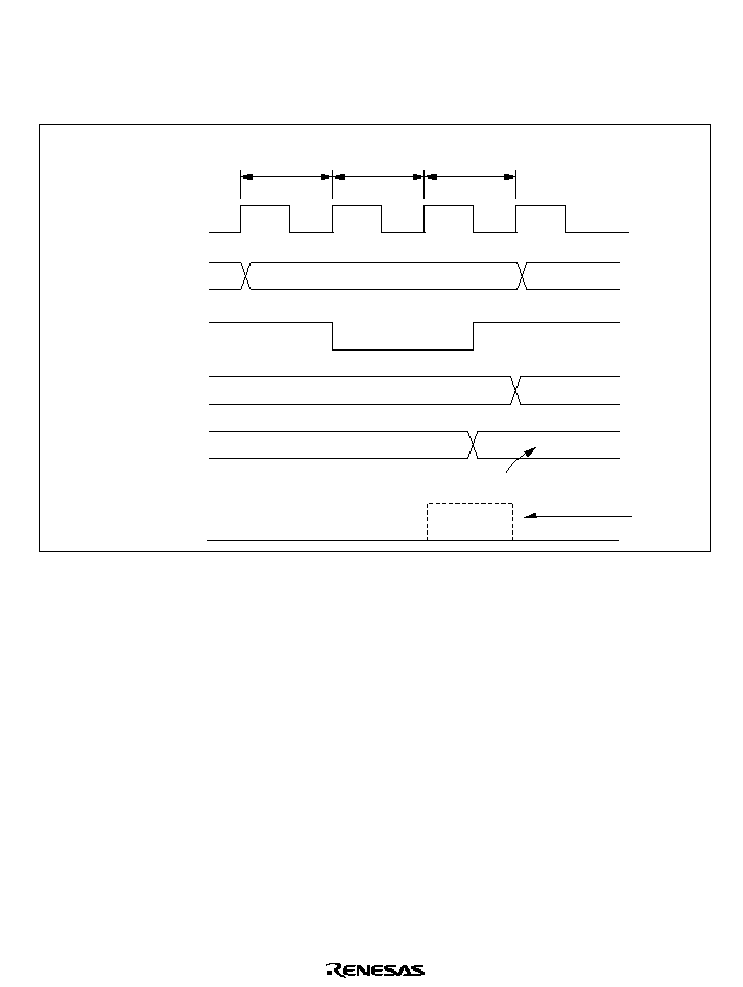
405
10.7.3
Contention between TCOR Write and Compare Match
If a compare match occurs in the T
3
state of a TCOR write cycle, writing takes priority and the
compare match signal is inhibited. Figure 10.20 shows the timing in this case.
Address bus
TCOR address
Internal write signal
8TCNT
TCOR
N
M
T
1
T
3
T
2
TCOR write cycle
TCOR write data
N
N+1
Compare match signal
Inhibited
Figure 10.20 Contention between TCOR Write and Compare Match
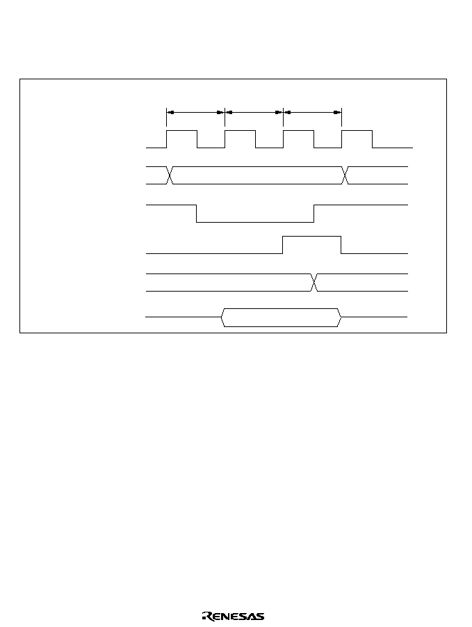
406
10.7.4
Contention between TCOR Read and Input Capture
If an input capture signal occurs in the T
3
state of a TCOR read cycle, the value before input
capture is read. Figure 10.21 shows the timing in this case.
Address bus
TCORB address
Internal read signal
Input capture signal
TCORB
N
M
T
1
T
3
T
2
TCORB read cycle
Internal data bus
N
Figure 10.21 Contention between TCOR Read and Input Capture
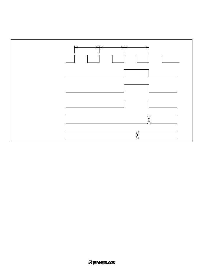
407
10.7.5
Contention between Counter Clearing by Input Capture and Counter Increment
If an input capture signal and counter increment signal occur simultaneously, counter clearing by
the input capture signal takes priority and the counter is not incremented. The value before the
counter is cleared is transferred to TCORB. Figure 10.22 shows the timing in this case.
Counter clear signal
8TCNT internal clock
8TCNT
N
X
H'00
T
1
T
3
T
2
Input capture signal
TCORB
N
Figure 10.22 Contention between Counter Clearing by Input Capture and Counter
Increment
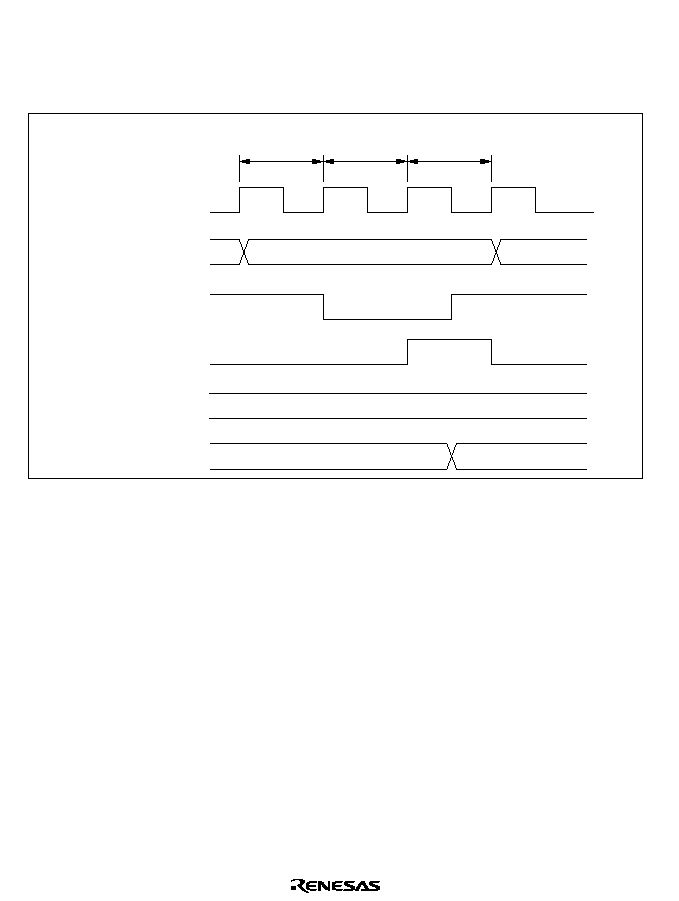
408
10.7.6
Contention between TCOR Write and Input Capture
If an input capture signal occurs in the T
3
state of a TCOR write cycle, input capture takes priority
and the write to TCOR is not performed. Figure 10.23 shows the timing in this case.
Address bus
TCOR address
Internal write signal
Input capture signal
8TCNT
M
T
1
T
3
T
2
TCOR write cycle
TCOR
M
X
Figure 10.23 Contention between TCOR Write and Input Capture
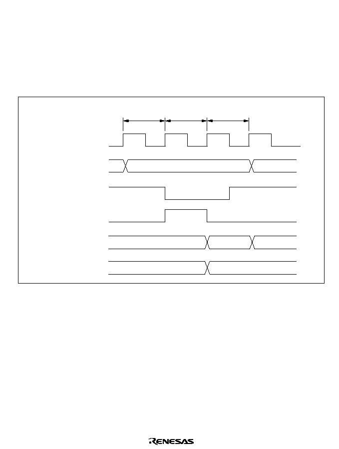
409
10.7.7
Contention between 8TCNT Byte Write and Increment in 16-Bit Count Mode
(Cascaded Connection)
If an increment pulse occurs in the T
3
state of an 8TCNT byte write cycle in 16-bit count mode,
the counter write takes priority and the byte data for which the write was performed is not
incremented. The byte data for which a write was not performed is incremented. Figure 10.24
shows the timing when an increment pulse occurs in the T
2
state of a byte write to 8TCNT (upper
byte). If an increment pulse occurs in the T
2
state, on the other hand, the increment takes priority.
Address bus
8TCNTH address
Internal write signal
8TCNT input clock
8TCNT (upper byte)
N
N+1
8TCNT write data
T
1
T
3
T
2
8TCNT (upper byte) byte write cycle
8TCNT (lower byte)
X+1
X
Figure 10.24 Contention between 8TCNT Byte Write and Increment in 16-Bit Count Mode
410
10.7.8
Contention between Compare Matches A and B
If compare matches A and B occur at the same time, the 8-bit timer operates according to the
relative priority of the output states set for compare match A and compare match B, as shown in
Table 10.7.
Table 10.7
Timer Output Priority Order
Priority
Output Setting
High
Toggle output
1 output
0 output
No change
Low
10.7.9
8TCNT Operation and Internal Clock Source Switchover
Switching internal clock sources may cause 8TCNT to increment, depending on the switchover
timing. Table 10.8 shows the relation between the time of the switchover (by writing to bits CKS1
and CKS0) and the operation of 8TCNT.
The 8TCNT input clock is generated from the internal clock source by detecting the rising edge of
the internal clock. If a switchover is made from a low clock source to a high clock source, as in
case No. 3 in Table 10.8, the switchover will be regarded as a falling edge, a 8TCNT clock pulse
will be generated, and 8TCNT will be incremented.
8TCNT may also be incremented when switching between internal and external clocks.
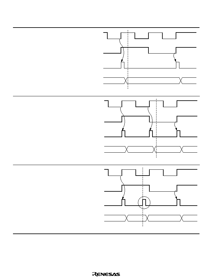
411
Table 10.8
Internal Clock Switchover and 8TCNT Operation
No.
CKS1 and CKS0 Write
Timing
8TCNT Operation
1
High
high switchover
*
1
Old clock
source
New clock
source
8TCNT clock
8TCNT
CKS bits rewritten
N
N+1
2
High
low switchover
*
2
Old clock
source
New clock
source
8TCNT clock
8TCNT
CKS bits rewritten
N
N+1
N+2
3
Low
high switchover
*
3
Old clock
source
New clock
source
8TCNT clock
8TCNT
CKS bits rewritten
N
N+1
N+2
*
4
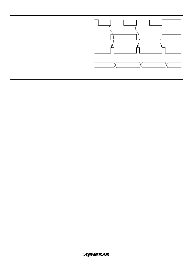
412
No.
CKS1 and CKS0 Write
Timing
8TCNT Operation
4
Low
low switchover
*
4
Old clock
source
New clock
source
8TCNT clock
8TCNT
CKS bits rewritten
N
N+1
N+2
Notes:
*
1 Including switchovers from the high level to the halted state, and from the halted state
to the high level.
*
2 Including switchover from the halted state to the low level.
*
3 Including switchover from the low level to the halted state.
*
4 The switchover is regarded as a rising edge, causing 8TCNT to increment.

413
Section 11 Programmable Timing Pattern Controller (TPC)
11.1
Overview
The H8/3069F has a built-in programmable timing pattern controller (TPC) that provides pulse
outputs by using the 16-bit timer as a time base. The TPC pulse outputs are divided into 4-bit
groups (group 3 to group 0) that can operate simultaneously and independently.
11.1.1
Features
TPC features are listed below.
�
16-bit output data
Maximum 16-bit data can be output. TPC output can be enabled on a bit-by-bit basis.
�
Four output groups
Output trigger signals can be selected in 4-bit groups to provide up to four different 4-bit
outputs.
�
Selectable output trigger signals
Output trigger signals can be selected for each group from the compare match signals of three
16-bit timer channels.
�
Non-overlap mode
A non-overlap margin can be provided between pulse outputs.
�
Can operate together with the DMA controller (DMAC)
The compare-match signals selected as trigger signals can activate the DMAC for sequential
output of data without CPU intervention.
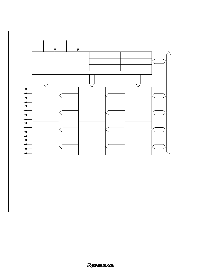
414
11.1.2
Block Diagram
Figure 11.1 shows a block diagram of the TPC.
PADDR
NDERA
TPMR
PBDDR
NDERB
TPCR
Internal
data bus
TP
TP
TP
TP
TP
TP
15
14
13
12
11
10
9
8
7
6
5
4
3
2
1
0
Control logic
16-bit timer compare match signals
Pulse output
pins, group 3
PBDR
PADR
Legend
TPMR:
TPCR:
NDERB:
NDERA:
PBDDR:
PADDR:
NDRB:
NDRA:
PBDR:
PADR:
Pulse output
pins, group 2
Pulse output
pins, group 1
Pulse output
pins, group 0
TPC output mode register
TPC output control register
Next data enable register B
Next data enable register A
Port B data direction register
Port A data direction register
Next data register B
Next data register A
Port B data register
Port A data register
NDRB
NDRA
TP
TP
TP
TP
TP
TP
TP
TP
TP
TP
Figure 11.1 TPC Block Diagram

415
11.1.3
TPC Pins
Table 11.1 summarizes the TPC output pins.
Table 11.1
TPC Pins
Name
Symbol
I/O
Function
TPC output 0
TP
0
Output
Group 0 pulse output
TPC output 1
TP
1
Output
TPC output 2
TP
2
Output
TPC output 3
TP
3
Output
TPC output 4
TP
4
Output
Group 1 pulse output
TPC output 5
TP
5
Output
TPC output 6
TP
6
Output
TPC output 7
TP
7
Output
TPC output 8
TP
8
Output
Group 2 pulse output
TPC output 9
TP
9
Output
TPC output 10
TP
10
Output
TPC output 11
TP
11
Output
TPC output 12
TP
12
Output
Group 3 pulse output
TPC output 13
TP
13
Output
TPC output 14
TP
14
Output
TPC output 15
TP
15
Output

416
11.1.4
Registers
Table 11.2 summarizes the TPC registers.
Table 11.2
TPC Registers
Address
*
1
Name
Abbreviation
R/W
Function
H'EE009
Port A data direction register
PADDR
W
H'00
H'FFFD9
Port A data register
PADR
R/(W)
*
2
H'00
H'EE00A
Port B data direction register
PBDDR
W
H'00
H'FFFDA
Port B data register
PBDR
R/(W)
*
2
H'00
H'FFFA0
TPC output mode register
TPMR
R/W
H'F0
H'FFFA1
TPC output control register
TPCR
R/W
H'FF
H'FFFA2
Next data enable register B
NDERB
R/W
H'00
H'FFFA3
Next data enable register A
NDERA
R/W
H'00
H'FFFA5/
H'FFFA7
*
3
Next data register A
NDRA
R/W
H'00
H'FFFA4/
H'FFFA6
*
3
Next data register B
NDRB
R/W
H'00
Notes:
*
1 Lower 20 bits of the address in advanced mode.
*
2 Bits used for TPC output cannot be written.
*
3 The NDRA address is H'FFFA5 when the same output trigger is selected for TPC
output groups 0 and 1 by settings in TPCR. When the output triggers are different, the
NDRA address is H'FFFA7 for group 0 and H'FFFA5 for group 1. Similarly, the address
of NDRB is H'FFFA4 when the same output trigger is selected for TPC output groups 2
and 3 by settings in TPCR. When the output triggers are different, the NDRB address is
H'FFFA6 for group 2 and H'FFFA4 for group 3.
417
11.2
Register Descriptions
11.2.1
Port A Data Direction Register (PADDR)
PADDR is an 8-bit write-only register that selects input or output for each pin in port A.
Bit
Initial value
Read/Write
7
PA DDR
0
W
Port A data direction 7 to 0
These bits select input or
output for port A pins
7
6
PA DDR
0
W
6
5
PA DDR
0
W
5
4
PA DDR
0
W
4
3
PA DDR
0
W
3
2
PA DDR
0
W
2
1
PA DDR
0
W
1
0
PA DDR
0
W
0
Port A is multiplexed with pins TP
7
to TP
0
. Bits corresponding to pins used for TPC output must
be set to 1. For further information about PADDR, see section 8.11, Port A.
11.2.2
Port A Data Register (PADR)
PADR is an 8-bit readable/writable register that stores TPC output data for groups 0 and 1, when
these TPC output groups are used.
Bit
Initial value
Read/Write
0
PA
0
R/(W)
0
1
PA
0
R/(W)
1
2
PA
0
R/(W)
2
3
PA
0
R/(W)
3
4
PA
0
R/(W)
4
5
PA
0
R/(W)
5
6
PA
0
R/(W)
6
7
PA
0
R/(W)
7
Port A data 7 to 0
These bits store output data
for TPC output groups 0 and 1
*
*
*
*
*
*
*
*
Note: Bits selected for TPC output by NDERA settings become read-only bits.
*
For further information about PADR, see section 8.11, Port A.
418
11.2.3
Port B Data Direction Register (PBDDR)
PBDDR is an 8-bit write-only register that selects input or output for each pin in port B.
Bit
Initial value
Read/Write
0
PB
0
DDR
0
W
1
PB
1
DDR
0
W
2
PB
2
DDR
0
W
3
PB
3
DDR
0
W
4
PB
4
DDR
0
W
5
PB
5
DDR
0
W
6
PB
6
DDR
0
W
7
PB
7
DDR
0
W
Port B direction 7 to 0
These bits select input or
output for port B pins
Port B is multiplexed with pins TP
15
to TP
8
. Bits corresponding to pins used for TPC output must
be set to 1. For further information about PBDDR, see section 8.12, Port B.
11.2.4
Port B Data Register (PBDR)
PBDR is an 8-bit readable/writable register that stores TPC output data for groups 2 and 3, when
these TPC output groups are used.
Bit
Initial value
Read/Write
Note:
*
Bits selected for TPC output by NDERB settings become read-only bits.
0
PB
0
0
R/(W)
*
1
PB
1
0
R/(W)
*
2
PB
2
0
R/(W)
*
3
PB
3
0
R/(W)
*
4
PB
4
0
R/(W)
*
5
PB
5
0
R/(W)
*
6
PB
6
0
R/(W)
*
7
PB
7
0
R/(W)
*
Port B data 7 to 0
These bits store output data
for TPC output groups 2 and 3
For further information about PBDR, see section 8.12, Port B.
419
11.2.5
Next Data Register A (NDRA)
NDRA is an 8-bit readable/writable register that stores the next output data for TPC output groups
1 and 0 (pins TP
7
to TP
0
). During TPC output, when an 16-bit timer compare match event
specified in TPCR occurs, NDRA contents are transferred to the corresponding bits in PADR. The
address of NDRA differs depending on whether TPC output groups 0 and 1 have the same output
trigger or different output triggers.
NDRA is initialized to H'00 by a reset and in hardware standby mode. It is not initialized in
software standby mode.
Same Trigger for TPC Output Groups 0 and 1: If TPC output groups 0 and 1 are triggered by
the same compare match event, the NDRA address is H'FFFA5. The upper 4 bits belong to group
1 and the lower 4 bits to group 0. Address H'FFFA7 consists entirely of reserved bits that cannot
be modified and always read 1.
Address H'FFFA5
Bit
Initial value
Read/Write
0
NDR0
0
R/W
1
NDR1
0
R/W
2
NDR2
0
R/W
3
NDR3
0
R/W
4
NDR4
0
R/W
5
NDR5
0
R/W
6
NDR6
0
R/W
7
NDR7
0
R/W
Next data 7 to 4
These bits store the next output
data for TPC output group 1
Next data 3 to 0
These bits store the next output
data for TPC output group 0
Address H'FFFA7
Bit
Initial value
Read/Write
0
--
1
--
1
--
1
--
2
--
1
--
3
--
1
--
4
--
1
--
5
--
1
--
6
--
1
--
7
--
1
--
Reserved bits

420
Different Triggers for TPC Output Groups 0 and 1: If TPC output groups 0 and 1 are triggered
by different compare match events, the address of the upper 4 bits of NDRA (group 1) is H'FFFA5
and the address of the lower 4 bits (group 0) is H'FFFA7. Bits 3 to 0 of address H'FFFA5 and bits
7 to 4 of address H'FFFA7 are reserved bits that cannot be modified and always read 1.
Address H'FFFA5
Bit
Initial value
Read/Write
0
--
1
--
1
--
1
--
2
--
1
--
3
--
1
--
4
NDR4
0
R/W
5
NDR5
0
R/W
6
NDR6
0
R/W
7
NDR7
0
R/W
Next data 7 to 4
These bits store the next output
data for TPC output group 1
Reserved bits
Address H'FFFA7
Bit
Initial value
Read/Write
0
NDR0
0
R/W
1
NDR1
0
R/W
2
NDR2
0
R/W
3
NDR3
0
R/W
4
--
1
--
5
--
1
--
6
--
1
--
7
--
1
--
Next data 3 to 0
These bits store the next output
data for TPC output group 0
Reserved bits

421
11.2.6
Next Data Register B (NDRB)
NDRB is an 8-bit readable/writable register that stores the next output data for TPC output groups
3 and 2 (pins TP
15
to TP
8
). During TPC output, when an 16-bit timer compare match event
specified in TPCR occurs, NDRB contents are transferred to the corresponding bits in PBDR. The
address of NDRB differs depending on whether TPC output groups 2 and 3 have the same output
trigger or different output triggers.
NDRB is initialized to H'00 by a reset and in hardware standby mode. It is not initialized in
software standby mode.
Same Trigger for TPC Output Groups 2 and 3: If TPC output groups 2 and 3 are triggered by
the same compare match event, the NDRB address is H'FFFA4. The upper 4 bits belong to group
3 and the lower 4 bits to group 2. Address H'FFFA6 consists entirely of reserved bits that cannot
be modified and always read 1.
Address H'FFFA4
Bit
Initial value
Read/Write
0
NDR8
0
R/W
1
NDR9
0
R/W
2
NDR10
0
R/W
3
NDR11
0
R/W
4
NDR12
0
R/W
5
NDR13
0
R/W
6
NDR14
0
R/W
7
NDR15
0
R/W
Next data 15 to 12
These bits store the next output
data for TPC output group 3
Next data 11 to 8
These bits store the next output
data for TPC output group 2
Address H'FFFA6
Bit
Initial value
Read/Write
0
--
1
--
1
--
1
--
2
--
1
--
3
--
1
--
4
--
1
--
5
--
1
--
6
--
1
--
7
--
1
--
Reserved bits
422
Different Triggers for TPC Output Groups 2 and 3: If TPC output groups 2 and 3 are triggered
by different compare match events, the address of the upper 4 bits of NDRB (group 3) is H'FFFA4
and the address of the lower 4 bits (group 2) is H'FFFA6. Bits 3 to 0 of address H'FFFA4 and bits
7 to 4 of address H'FFFA6 are reserved bits that cannot be modified and always read 1.
Address H'FFFA4
Bit
Initial value
Read/Write
0
--
1
--
1
--
1
--
2
--
1
--
3
--
1
--
4
NDR12
0
R/W
5
NDR13
0
R/W
6
NDR14
0
R/W
7
NDR15
0
R/W
Next data 15 to 12
These bits store the next output
data for TPC output group 3
Reserved bits
Address H'FFFA6
Bit
Initial value
Read/Write
0
NDR8
0
R/W
1
NDR9
0
R/W
2
NDR10
0
R/W
3
NDR11
0
R/W
4
--
1
--
5
--
1
--
6
--
1
--
7
--
1
--
Next data 11 to 8
These bits store the next output
data for TPC output group 2
Reserved bits

423
11.2.7
Next Data Enable Register A (NDERA)
NDERA is an 8-bit readable/writable register that enables or disables TPC output groups 1 and 0
(TP
7
to TP
0
) on a bit-by-bit basis.
Bit
Initial value
Read/Write
0
NDER0
0
R/W
1
NDER1
0
R/W
2
NDER2
0
R/W
3
NDER3
0
R/W
4
NDER4
0
R/W
5
NDER5
0
R/W
6
NDER6
0
R/W
7
NDER7
0
R/W
Next data enable 7 to 0
These bits enable or disable
TPC output groups 1 and 0
If a bit is enabled for TPC output by NDERA, then when the 16-bit timer compare match event
selected in the TPC output control register (TPCR) occurs, the NDRA value is automatically
transferred to the corresponding PADR bit, updating the output value. If TPC output is disabled,
the bit value is not transferred from NDRA to PADR and the output value does not change.
NDERA is initialized to H'00 by a reset and in hardware standby mode. It is not initialized in
software standby mode.
Bits 7 to 0--Next Data Enable 7 to 0 (NDER7 to NDER0): These bits enable or disable TPC
output groups 1 and 0 (TP
7
to TP
0
) on a bit-by-bit basis.
Bits 7 to 0
NDER7 to NDER0
Description
0
TPC outputs TP
7
to TP
0
are disabled
(NDR7 to NDR0 are not transferred to PA
7
to PA
0
)
(Initial value)
1
TPC outputs TP
7
to TP
0
are enabled
(NDR7 to NDR0 are transferred to PA
7
to PA
0
)

424
11.2.8 Next Data Enable Register B (NDERB)
NDERB is an 8-bit readable/writable register that enables or disables TPC output groups 3 and 2
(TP
15
to TP
8
) on a bit-by-bit basis.
Bit
Initial value
Read/Write
0
NDER8
0
R/W
1
NDER9
0
R/W
2
NDER10
0
R/W
3
NDER11
0
R/W
4
NDER12
0
R/W
5
NDER13
0
R/W
6
NDER14
0
R/W
7
NDER15
0
R/W
Next data enable 15 to 8
These bits enable or disable
TPC output groups 3 and 2
If a bit is enabled for TPC output by NDERB, then when the 16-bit timer compare match event
selected in the TPC output control register (TPCR) occurs, the NDRB value is automatically
transferred to the corresponding PBDR bit, updating the output value. If TPC output is disabled,
the bit value is not transferred from NDRB to PBDR and the output value does not change.
NDERB is initialized to H'00 by a reset and in hardware standby mode. It is not initialized in
software standby mode.
Bits 7 to 0--Next Data Enable 15 to 8 (NDER15 to NDER8): These bits enable or disable TPC
output groups 3 and 2 (TP
15
to TP
8
) on a bit-by-bit basis.
Bits 7 to 0
NDER15 to NDER8
Description
0
TPC outputs TP
15
to TP
8
are disabled
(NDR15 to NDR8 are not transferred to PB
7
to PB
0
)
(Initial value)
1
TPC outputs TP
15
to TP
8
are enabled
(NDR15 to NDR8 are transferred to PB
7
to PB
0
)

425
11.2.9
TPC Output Control Register (TPCR)
TPCR is an 8-bit readable/writable register that selects output trigger signals for TPC outputs on a
group-by-group basis.
Bit
Initial value
Read/Write
0
G0CMS0
1
R/W
1
G0CMS1
1
R/W
2
G1CMS0
1
R/W
3
G1CMS1
1
R/W
4
G2CMS0
1
R/W
5
G2CMS1
1
R/W
6
G3CMS0
1
R/W
7
G3CMS1
1
R/W
Group 3 compare
match select 1 and 0
These bits select
the compare match
event that triggers
TPC output group 3
(TP
15
to TP
12
)
Group 2 compare
match select 1 and 0
These bits select
the compare match
event that triggers
TPC output group 2
(TP
11
to TP
8
)
Group 1 compare
match select 1 and 0
These bits select
the compare match
event that triggers
TPC output group 1
(TP
7
to TP
4
)
Group 0 compare
match select 1 and 0
These bits select
the compare match
event that triggers
TPC output group 0
(TP
3
to TP
0
)
TPCR is initialized to H'FF by a reset and in hardware standby mode. It is not initialized in
software standby mode.

426
Bits 7 and 6--Group 3 Compare Match Select 1 and 0 (G3CMS1, G3CMS0): These bits
select the compare match event that triggers TPC output group 3 (TP
15
to TP
12
).
Bit 7
G3CMS1
Bit 6
G3CMS0
Description
0
0
TPC output group 3 (TP
15
to TP
12
) is triggered by compare match in 16-bit
timer channel 0
1
TPC output group 3 (TP
15
to TP
12
) is triggered by compare match in 16-bit
timer channel 1
1
0
TPC output group 3 (TP
15
to TP
12
) is triggered by compare match in 16-bit
timer channel 2
1
TPC output group 3 (TP
15
to TP
12
) is triggered by
compare match in 16-bit timer channel 2
(Initial value)
Bits 5 and 4--Group 2 Compare Match Select 1 and 0 (G2CMS1, G2CMS0): These bits
select the compare match event that triggers TPC output group 2 (TP
11
to TP
8
).
Bit 5
G2CMS1
Bit 4
G2CMS0
Description
0
0
TPC output group 2 (TP
11
to TP
8
) is triggered by compare match in 16-bit
timer channel 0
1
TPC output group 2 (TP
11
to TP
8
) is triggered by compare match in 16-bit
timer channel 1
1
0
TPC output group 2 (TP
11
to TP
8
) is triggered by compare match in 16-bit
timer channel 2
1
TPC output group 2 (TP
11
to TP
8
) is triggered by
compare match in 16-bit timer channel 2
(Initial value)

427
Bits 3 and 2--Group 1 Compare Match Select 1 and 0 (G1CMS1, G1CMS0): These bits
select the compare match event that triggers TPC output group 1 (TP
7
to TP
4
).
Bit 3
G1CMS1
Bit 2
G1CMS0
Description
0
0
TPC output group 1 (TP
7
to TP
4
) is triggered by compare match in 16-bit
timer channel 0
1
TPC output group 1 (TP
7
to TP
4
) is triggered by compare match in 16-bit
timer channel 1
1
0
TPC output group 1 (TP
7
to TP
4
) is triggered by compare match in 16-bit
timer channel 2
1
TPC output group 1 (TP
7
to TP
4
) is triggered by
compare match in 16-bit timer channel 2
(Initial value)
Bits 1 and 0--Group 0 Compare Match Select 1 and 0 (G0CMS1, G0CMS0): These bits
select the compare match event that triggers TPC output group 0 (TP
3
to TP
0
).
Bit 1
G0CMS1
Bit 0
G0CMS0
Description
0
0
TPC output group 0 (TP
3
to TP
0
) is triggered by compare match in 16-bit
timer channel 0
1
TPC output group 0 (TP
3
to TP
0
) is triggered by compare match in 16-bit
timer channel 1
1
0
TPC output group 0 (TP
3
to TP
0
) is triggered by compare match in 16-bit
timer channel 2
1
TPC output group 0 (TP
3
to TP
0
) is triggered by
compare match in 16-bit timer channel 2
(Initial value)
428
11.2.10
TPC Output Mode Register (TPMR)
TPMR is an 8-bit readable/writable register that selects normal or non-overlapping TPC output for
each group.
Bit
Initial value
Read/Write
7
--
1
--
6
--
1
--
5
--
1
--
4
--
1
--
3
G3NOV
0
R/W
0
G0NOV
0
R/W
2
G2NOV
0
R/W
1
G1NOV
0
R/W
Group 3 non-overlap
Selects non-overlapping TPC
output for group 3 (TP to TP )
Reserved bits
Group 2 non-overlap
Selects non-overlapping TPC
output for group 2 (TP to TP )
Group 1 non-overlap
Selects non-overlapping TPC
output for group 1 (TP to TP )
Group 0 non-overlap
Selects non-overlapping TPC
output for group 0 (TP to TP )
15
12
11
8
7
4
3
0
The output trigger period of a non-overlapping TPC output waveform is set in general register B
(GRB) in the 16-bit timer channel selected for output triggering. The non-overlap margin is set in
general register A (GRA). The output values change at compare match A and B. For details see
section 11.3.4, Non-Overlapping TPC Output.
TPMR is initialized to H'F0 by a reset and in hardware standby mode. It is not initialized in
software standby mode.
Bits 7 to 4--Reserved: These bits cannot be modified and are always read as 1.

429
Bit 3--Group 3 Non-Overlap (G3NOV): Selects normal or non-overlapping TPC output for
group 3 (TP
15
to TP
12
).
Bit 3
G3NOV
Description
0
Normal TPC output in group 3 (output values change at
compare match A in the selected 16-bit timer channel)
(Initial value)
1
Non-overlapping TPC output in group 3 (independent 1 and 0 output at
compare match A and B in the selected 16-bit timer channel)
Bit 2--Group 2 Non-Overlap (G2NOV): Selects normal or non-overlapping TPC output for
group 2 (TP
11
to TP
8
).
Bit 2
G2NOV
Description
0
Normal TPC output in group 2 (output values change at
compare match A in the selected 16-bit timer channel)
(Initial value)
1
Non-overlapping TPC output in group 2 (independent 1 and 0 output at
compare match A and B in the selected 16-bit timer channel)
Bit 1--Group 1 Non-Overlap (G1NOV): Selects normal or non-overlapping TPC output for
group 1 (TP
7
to TP
4
).
Bit 1
G1NOV
Description
0
Normal TPC output in group 1 (output values change at
compare match A in the selected 16-bit timer channel)
(Initial value)
1
Non-overlapping TPC output in group 1 (independent 1 and 0 output at
compare match A and B in the selected 16-bit timer channel)
Bit 0--Group 0 Non-Overlap (G0NOV): Selects normal or non-overlapping TPC output for
group 0 (TP
3
to TP
0
).
Bit 0
G0NOV
Description
0
Normal TPC output in group 0 (output values change at
compare match A in the selected 16-bit timer channel)
(Initial value)
1
Non-overlapping TPC output in group 0 (independent 1 and 0 output at
compare match A and B in the selected 16-bit timer channel)
430
11.3
Operation
11.3.1
Overview
When corresponding bits in PADDR or PBDDR and NDERA or NDERB are set to 1, TPC output
is enabled. The TPC output initially consists of the corresponding PADR or PBDR contents.
When a compare-match event selected in TPCR occurs, the corresponding NDRA or NDRB bit
contents are transferred to PADR or PBDR to update the output values.
Figure 11.2 illustrates the TPC output operation. Table 11.3 summarizes the TPC operating
conditions.
DDR
NDER
Q
Q
TPC output pin
DR
NDR
C
Q
D
Q
D
Internal
data bus
Output trigger signal
Figure 11.2 TPC Output Operation
Table 11.3
TPC Operating Conditions
NDER
DDR
Pin Function
0
0
Generic input port
1
Generic output port
1
0
Generic input port (but the DR bit is a read-only bit, and when compare
match occurs, the NDR bit value is transferred to the DR bit)
1
TPC pulse output
Sequential output of up to 16-bit patterns is possible by writing new output data to NDRA and
NDRB before the next compare match. For information on non-overlapping operation, see
section 11.3.4, Non-Overlapping TPC Output.
431
11.3.2
Output Timing
If TPC output is enabled, NDRA/NDRB contents are transferred to PADR/PBDR and output
when the selected compare match event occurs. Figure 11.3 shows the timing of these operations
for the case of normal output in groups 2 and 3, triggered by compare match A.
TCNT
GRA
Compare
match A signal
NDRB
PBDR
TP to TP
8
15
N
N
n
m
m
N + 1
n
n
Figure 11.3 Timing of Transfer of Next Data Register Contents and Output (Example)
432
11.3.3
Normal TPC Output
Sample Setup Procedure for Normal TPC Output: Figure 11.4 shows a sample procedure for
setting up normal TPC output.
Normal TPC output
Set next TPC output data
Compare match?
No
Yes
Set next TPC output data
16-bit timer
setup
16-bit timer
setup
Port and
TPC setup
10
11
9
1.
2.
3.
4.
5.
6.
7.
8.
9.
10.
11.
Set TIOR to make GRA an output compare
register (with output inhibited).
Set the TPC output trigger period.
Select the counter clock source with bits
TPSC2 to TPSC0 in TCR. Select the counter
clear source with bits CCLR1 and CCLR0.
Enable the IMFA interrupt in TISRA.
The DMAC can also be set up to transfer
data to the next data register.
Set the initial output values in the DR bits
of the input/output port pins to be used for
TPC output.
Set the DDR bits of the input/output port
pins to be used for TPC output to 1.
Set the NDER bits of the pins to be used for
TPC output to 1.
Select the 16-bit timer compare match event
to be used as the TPC output trigger in TPCR.
Set the next TPC output values in the NDR bits.
Set the STR bit to 1 in TSTR to start the
timer counter.
At each IMFA interrupt, set the next output
values in the NDR bits.
1
2
3
4
5
6
7
8
Select GR functions
Set GRA value
Select counting operation
Select interrupt request
Start counter
Set initial output data
Select port output
Enable TPC output
Select TPC output trigger
Figure 11.4 Setup Procedure for Normal TPC Output (Example)

433
Example of Normal TPC Output (Example of Five-Phase Pulse Output): Figure 11.5 shows
an example in which the TPC is used for cyclic five-phase pulse output.
GRA
H'0000
NDRB
PBDR
TP
15
TP
14
TP
13
TP
12
TP
11
�
�
�
�
Time
80
TCNT
TCNT value
C0
40
60
20
30
10
18
08
88
80
C0
Compare match
The 16-bit timer channel to be used as the output trigger channel is set up so that GRA is an output
compare register and the counter will be cleared by compare match A. The trigger period is set in GRA.
The IMIEA bit is set to 1 in TISRA to enable the compare match A interrupt.
H'F8 is written in PBDDR and NDERB, and bits G3CMS1, G3CMS0, G2CMS1, and G2CMS0 are set in
TPCR to select compare match in the 16-bit timer channel set up in step 1 as the output trigger.
Output data H'80 is written in NDRB.
The timer counter in this 16-bit timer channel is started. When compare match A occurs, the NDRB
contents are transferred to PBDR and output. The compare match/input capture A (IMFA) interrupt
service routine writes the next output data (H'C0) in NDRB.
Five-phase overlapping pulse output (one or two phases active at a time) can be obtained by writing
H'40, H'60, H'20, H'30, H'10, H'18, H'08, H'88... at successive IMFA interrupts. If the DMAC is set for
activation by this interrupt, pulse output can be obtained without loading the CPU.
00
80
C0
40
60
20
30
10
18
08
88
80
C0
40
Figure 11.5 Normal TPC Output Example (Five-Phase Pulse Output)
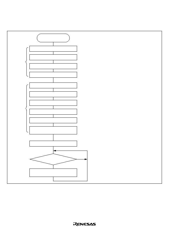
434
11.3.4
Non-Overlapping TPC Output
Sample Setup Procedure for Non-Overlapping TPC Output: Figure 11.6 shows a sample
procedure for setting up non-overlapping TPC output.
Non-overlapping
TPC output
Set next TPC output data
Compare match A?
No
Yes
Set next TPC output data
Start counter
16-bit timer
setup
16-bit timer
setup
Port and
TPC setup
Set initial output data
Set up TPC output
Enable TPC transfer
Select TPC transfer trigger
Select non-overlapping groups
1
2
3
4
12
10
11
5
6
7
8
9
1.
2.
3.
4.
5.
6.
7.
8.
9.
10.
11.
12.
Set TIOR to make GRA and GRB output
compare registers (with output inhibited).
Set the TPC output trigger period in GRB
and the non-overlap margin in GRA.
Select the counter clock source with bits
TPSC2 to TPSC0 in TCR. Select the counter
clear source with bits CCLR1 and CCLR0.
Enable the IMFA interrupt in TISRA.
The DMAC can also be set up to transfer
data to the next data register.
Set the initial output values in the DR bits
of the input/output port pins to be used for
TPC output.
Set the DDR bits of the input/output port pins
to be used for TPC output to 1.
Set the NDER bits of the pins to be used for
TPC output to 1.
In TPCR, select the 16-bit timer compare match
event to be used as the TPC output trigger.
In TPMR, select the groups that will operate
in non-overlap mode.
Set the next TPC output values in the NDR
bits.
Set the STR bit to 1 in TSTR to start the timer
counter.
At each IMFA interrupt, write the next output
value in the NDR bits.
Select GR functions
Set GR values
Select counting operation
Select interrupt requests
Figure 11.6 Setup Procedure for Non-Overlapping TPC Output (Example)
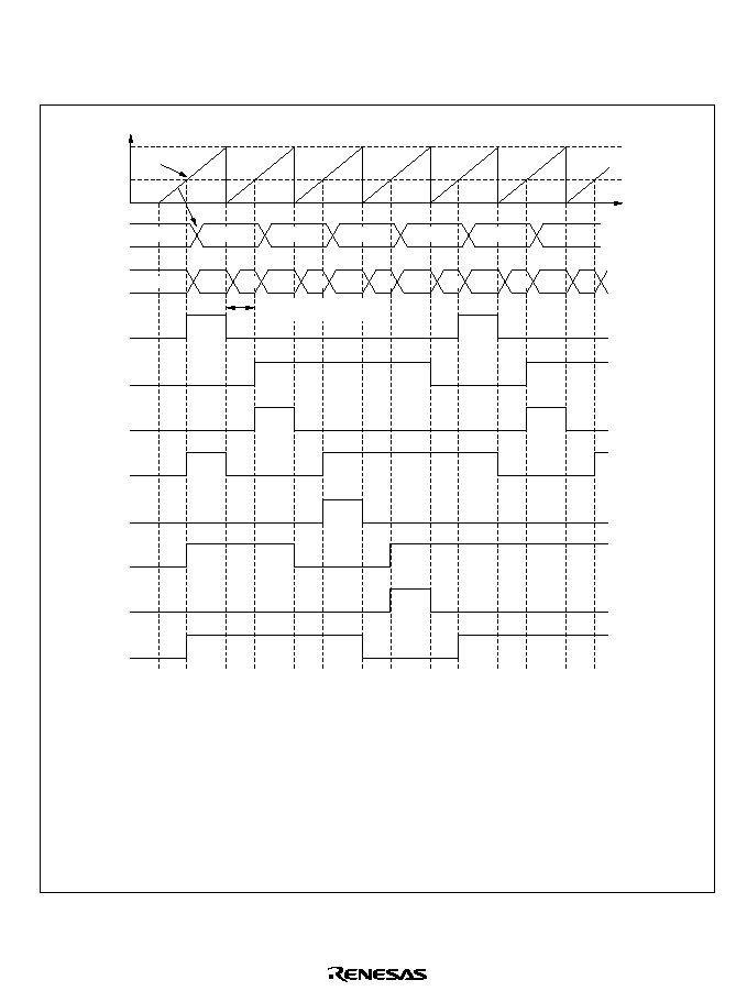
435
Example of Non-Overlapping TPC Output (Example of Four-Phase Complementary Non-
Overlapping Output): Figure 11.7 shows an example of the use of TPC output for four-phase
complementary non-overlapping pulse output.
GRB
H'0000
NDRB
PBDR
TP
15
TP
14
TP
13
TP
12
TP
11
TP
10
TP
9
TP
8
Time
95
00
65
95
59
56
95
65
05
65
41
59
50
56
14
95
05
65
TCNT
period is set in GRB. The non-overlap margin is set in GRA. The IMIEA bit is set to 1 in TISRA to enable
IMFA interrupts.
H'FF is written in PBDDR and NDERB, and bits G3CMS1, G3CMS0, G2CMS1, and G2CMS0 are set in
TPCR to select compare match in the 16-bit timer channel set up in step 1 as the output trigger. Bits
G3NOV and G2NOV are set to 1 in TPMR to select non-overlapping output. Output data H'95 is written in
NDRB.
TCNT value
Non-overlap margin
The 16-bit timer channel to be used as the output trigger channel is set up so that GRA and GRB are
output compare registers and the counter will be cleared by compare match B. The TPC output trigger
�
�
�
�
The timer counter in this 16-bit timer channel is started. When compare match B occurs, outputs change
from 1 to 0. When compare match A occurs, outputs change from 0 to 1 (the change from 0 to 1 is delayed
by the value of GRA). The IMFA interrupt service routine writes the next output data (H'65) in NDRB.
Four-phase complementary non-overlapping pulse output can be obtained by writing H'59, H'56, H'95...
at successive IMFA interrupts. If the DMAC is set for activation by this interrupt, pulse output can be
obtained without loading the CPU.
GRA
Figure 11.7 Non-Overlapping TPC Output Example (Four-Phase Complementary
Non-Overlapping Pulse Output)
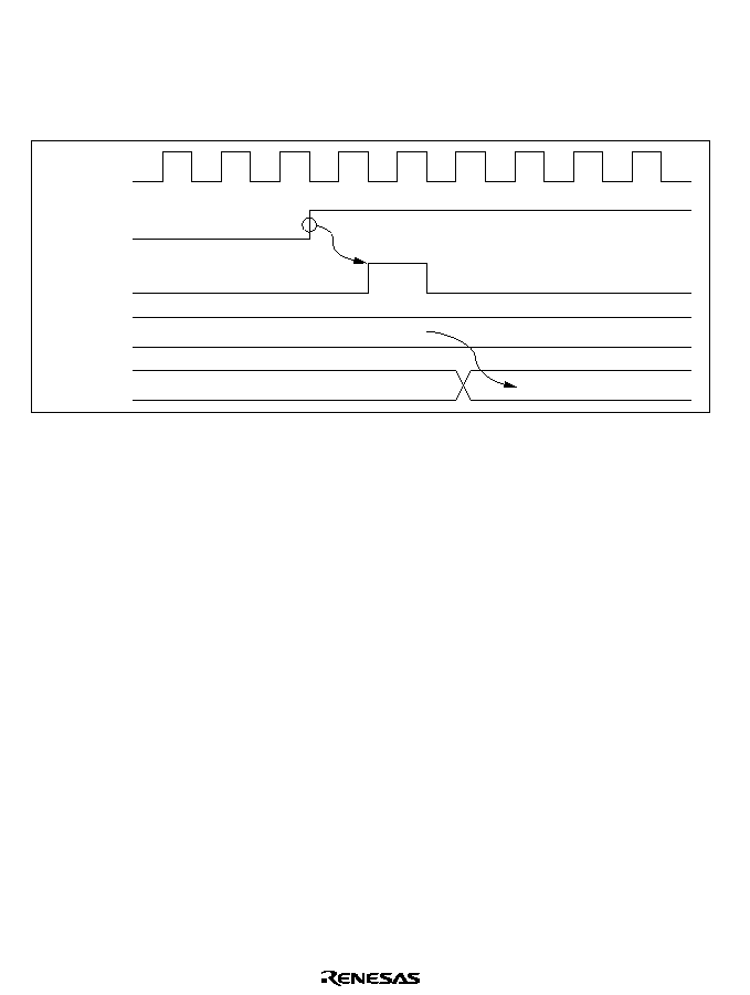
436
11.3.5
TPC Output Triggering by Input Capture
TPC output can be triggered by 16-bit timer input capture as well as by compare match. If GRA
functions as an input capture register in the 16-bit timer channel selected in TPCR, TPC output
will be triggered by the input capture signal. Figure 11.8 shows the timing.
TIOC pin
Input capture
signal
NDR
DR
N
N
M
Figure 11.8 TPC Output Triggering by Input Capture (Example)
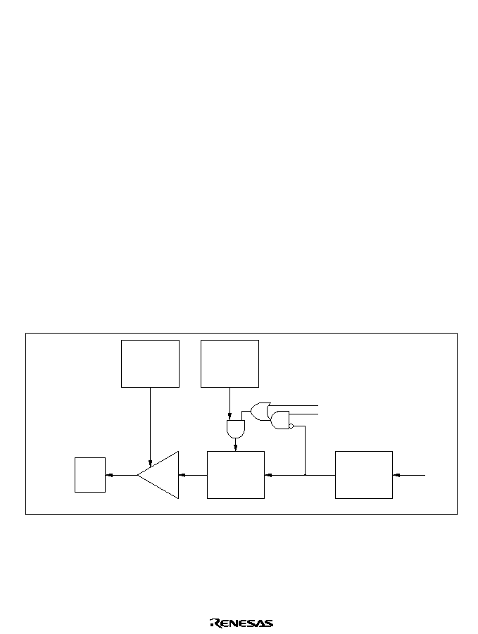
437
11.4
Usage Notes
11.4.1
Operation of TPC Output Pins
TP
0
to TP
15
are multiplexed with 16-bit timer, DMAC, address bus, and other pin functions. When
16-bit timer, DMAC, or address output is enabled, the corresponding pins cannot be used for TPC
output. The data transfer from NDR bits to DR bits takes place, however, regardless of the usage
of the pin.
Pin functions should be changed only under conditions in which the output trigger event will not
occur.
11.4.2
Note on Non-Overlapping Output
During non-overlapping operation, the transfer of NDR bit values to DR bits takes place as
follows.
1. NDR bits are always transferred to DR bits at compare match A.
2. At compare match B, NDR bits are transferred only if their value is 0. Bits are not transferred
if their value is 1.
Figure 11.9 illustrates the non-overlapping TPC output operation.
DDR
NDER
Q
Q
TPC output pin
DR
NDR
C
Q
D
Q
D
Compare match A
Compare match B
Figure 11.9 Non-Overlapping TPC Output
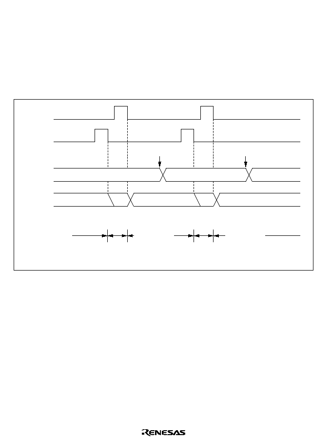
438
Therefore, 0 data can be transferred ahead of 1 data by making compare match B occur before
compare match A. NDR contents should not be altered during the interval from compare match B
to compare match A (the non-overlap margin).
This can be accomplished by having the IMFA interrupt service routine write the next data in
NDR, or by having the IMFA interrupt activate the DMAC. The next data must be written before
the next compare match B occurs.
Figure 11.10 shows the timing relationships.
Compare
match A
Compare
match B
NDR write
NDR
NDR write
DR
0/1 output
0/1 output
0 output
0 output
Do not write
to NDR in this
interval
Do not write
to NDR in this
interval
Write to NDR
in this interval
Write to NDR
in this interval
Figure 11.10 Non-Overlapping Operation and NDR Write Timing

439
Section 12 Watchdog Timer
12.1
Overview
The H8/3069F has an on-chip watchdog timer (WDT). The WDT has two selectable functions: it
can operate as a watchdog timer to supervise system operation, or it can operate as an interval
timer. As a watchdog timer, it generates a reset signal for the H8/3069F chip if a system crash
allows the timer counter (TCNT) to overflow before being rewritten. In interval timer operation,
an interval timer interrupt is requested at each TCNT overflow.
12.1.1
Features
WDT features are listed below.
�
Selection of eight counter clock sources
/2,
/32,
/64,
/128,
/256,
/512,
/2048, or
/4096
�
Interval timer option
�
Timer counter overflow generates a reset signal or interrupt.
The reset signal is generated in watchdog timer operation. An interval timer interrupt is
generated in interval timer operation.
�
Watchdog timer reset signal resets the entire H8/3069F internally.
The reset signal generated by timer counter overflow during watchdog timer operation resets
the entire H8/3069F internally.
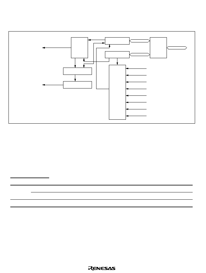
440
12.1.2
Block Diagram
Figure 12.1 shows a block diagram of the WDT.
/2
/32
/64
/128
/256
/512
/2048
/4096
TCNT
TCSR
RSTCSR
Reset control
Interrupt signal
Reset
(internal)
(interval timer)
Interrupt
control
Overflow
Clock
Clock
selector
Read/
write
control
Internal
data bus
Internal clock sources
Legend
TCNT:
TCSR:
RSTCSR:
Timer counter
Timer control/status register
Reset control/status register
Figure 12.1 WDT Block Diagram
12.1.3
Register Configuration
Table 12.1 summarizes the WDT registers.
Table 12.1
WDT Registers
Address
*
1
Write
*
2
Read
Name
Abbreviation
R/W
Initial Value
H'FFF8C H'FFF8C Timer control/status register
TCSR
R/(W)
*
3
H'18
H'FFF8D Timer counter
TCNT
R/W
H'00
H'FFF8E H'FFF8F Reset control/status register
RSTCSR
R/(W)
*
3
H'3F
Notes:
*
1 Lower 20 bits of the address in advanced mode.
*
2 Write word data starting at this address.
*
3 Only 0 can be written in bit 7, to clear the flag.

441
12.2
Register Descriptions
12.2.1
Timer Counter (TCNT)
TCNT is an 8-bit readable and writable up-counter.
Bit
Initial value
Read/Write
Note: TCNT is write-protected by a password. For details see section 12.2.4, Notes on Register
Access.
7
0
R/W
6
0
R/W
5
0
R/W
4
0
R/W
3
0
R/W
0
0
R/W
2
0
R/W
1
0
R/W
When the TME bit is set to 1 in TCSR, TCNT starts counting pulses generated from an internal
clock source selected by bits CKS2 to CKS0 in TCSR. When the count overflows (changes from
H'FF to H'00), the OVF bit is set to 1 in TCSR. TCNT is initialized to H'00 by a reset and when
the TME bit is cleared to 0.

442
12.2.2
Timer Control/Status Register (TCSR)
TCSR is an 8-bit readable and writable register. Its functions include selecting the timer mode and
clock source.
Bit
Initial value
Read/Write
Notes: TCSR is write-protected by a password. For details see section 12.2.4, Notes on Register
Access.
*
Only 0 can be written, to clear the flag.
7
OVF
0
R/(W)
6
WT/IT
0
R/W
5
TME
0
R/W
4
--
1
--
3
--
1
--
0
CKS0
0
R/W
2
CKS2
0
R/W
1
CKS1
0
R/W
Overflow flag
Status flag indicating overflow
Clock select
These bits select the
TCNT clock source
Timer mode select
Selects the mode
Timer enable
Selects whether TCNT runs or halts
Reserved bits
*
Bits 7 to 5 are initialized to 0 by a reset and in standby mode. Bits 2 to 0 are initialized to 0 by a
reset. In software standby mode bits 2 to 0 are not initialized, but retain their previous values.

443
Bit 7--Overflow Flag (OVF): This status flag indicates that the timer counter has overflowed
from H'FF to H'00.
Bit 7
OVF
Description
0
[Clearing condition]
Cleared by reading OVF when OVF = 1, then writing 0 in OVF
(Initial value)
1
[Setting condition]
Set when TCNT changes from H'FF to H'00
Bit 6--Timer Mode Select (WT/
IT): Selects whether to use the WDT as a watchdog timer or
interval timer. If used as an interval timer, the WDT generates an interval timer interrupt request
when TCNT overflows. If used as a watchdog timer, the WDT generates a reset signal when
TCNT overflows.
Bit 6
WT/
IT
Description
0
Interval timer: requests interval timer interrupts
(Initial value)
1
Watchdog timer: generates a reset signal
Bit 5--Timer Enable (TME): Selects whether TCNT runs or is halted. When WT/
IT = 1, clear
the software standby bit (SSBY) to 0 in SYSCR before setting TME. When setting SSBY to 1,
TME should be cleared to 0.
Bit 5
TME
Description
0
TCNT is initialized to H'00 and halted
(Initial value)
1
TCNT is counting
Bits 4 and 3--Reserved: These bits cannot be modified and are always read as 1.
444
Bits 2 to 0--Clock Select 2 to 0 (CKS2/1/0): These bits select one of eight internal clock sources,
obtained by prescaling the system clock (
), for input to TCNT.
Bit 2
CKS2
Bit 1
CKS1
Bit 0
CKS0
Description
0
0
0
/2
(Initial value)
1
/32
1
0
/64
1
/128
1
0
0
/256
1
/512
1
0
/2048
1
/4096
12.2.3
Reset Control/Status Register (RSTCSR)
RSTCSR is an 8-bit readable and writable register that indicates when a reset signal has been
generated by watchdog timer overflow, and controls external output of the reset signal.
Bit
Initial value
Read/Write
Notes: RSTCSR is write-protected by a password. For details see section 12.2.4, Notes on
Register Access.
*
Only 0 can be written in bit 7, to clear the flag.
7
WRST
0
R/(W)
*
6
--
0
R/W
5
--
1
--
4
--
1
--
3
--
1
--
0
--
1
--
2
--
1
--
1
--
1
--
Watchdog timer reset
Indicates that a reset signal has been generated
Reserved bits
Bits 7 and 6 are initialized by input of a reset signal at the
RES pin. They are not initialized by
reset signals generated by watchdog timer overflow.
445
Bit 7--Watchdog Timer Reset (WRST): During watchdog timer operation, this bit indicates that
TCNT has overflowed and generated a reset signal. This reset signal resets the entire H8/3068F
chip internally.
Bit 7
WRST
Description
0
[Clearing condition]
Reset signal at
RES
pin.
Read WRST when WRST =1, then write 0 in WRST.
(Initial value)
1
[Setting condition]
Set when TCNT overflow generates a reset signal during watchdog timer operation
Bit 6--Reserved: The write value should always be 0.
Bits 5 to 0--Reserved: These bits are always read as 1. The write value should always be 1.
12.2.4
Notes on Register Access
The watchdog timer's TCNT, TCSR, and RSTCSR registers differ from other registers in being
more difficult to write. The procedures for writing and reading these registers are given below.
Writing to TCNT and TCSR: These registers must be written by a word transfer instruction.
They cannot be written by byte instructions. Figure 12.2 shows the format of data written to TCNT
and TCSR. TCNT and TCSR both have the same write address. The write data must be contained
in the lower byte of the written word. The upper byte must contain H'5A (password for TCNT) or
H'A5 (password for TCSR). This transfers the write data from the lower byte to TCNT or TCSR.
15
8 7
0
H'5A
Write data
Address
H'FFF8C
*
15
8 7
0
H'A5
Write data
Address
H'FFF8C
*
TCNT write
TCSR write
Note: Lower 20 bits of the address in advanced mode.
*
Figure 12.2 Format of Data Written to TCNT and TCSR

446
Writing to RSTCSR: RSTCSR must be written by a word transfer instruction. It cannot be
written by byte transfer instructions. Figure 12.3 shows the format of data written to RSTCSR. To
write 0 in the WRST bit, the write data must have H'A5 in the upper byte and H'00 in the lower
byte. The data (H'00) in the lower byte is written to RSTCSR, clearing the WRST bit to 0. To
write to the RSTOE bit, the upper byte must contain H'5A and the lower byte must contain the
write data. Writing this word transfers a write data value into the RSTOE bit.
15
8 7
0
H'A5
H'00
Address
H'FFF8E
*
15
8 7
0
H'5A
Write data
Address
H'FFF8E
*
Writing 0 in WRST bit
Writing to RSTOE bit
Note: Lower 20 bits of the address in advanced mode.
*
Figure 12.3 Format of Data Written to RSTCSR
Reading TCNT, TCSR, and RSTCSR: These registers are read like other registers. Reading
TCNT, TCSR, and RSTCSR: These registers are read like other registers. Byte transfer
instructions can be used. The read addresses are H'FFF8C for TCSR, H'FFF8D for TCNT, and
H'FFF8F for RSTCSR, as listed in table 12.2.
Table 12.2
Read Addresses of TCNT, TCSR, and RSTCSR
Address
*
Register
H'FFF8C
TCSR
H'FFF8D
TCNT
H'FFF8F
RSTCSR
Note:
*
Lower 20 bits of the address in advanced mode.
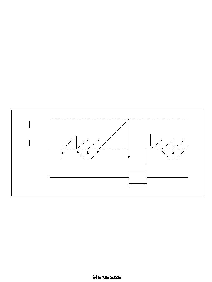
447
12.3
Operation
Operations when the WDT is used as a watchdog timer and as an interval timer are described
below.
12.3.1
Watchdog Timer Operation
Figure 12.4 illustrates watchdog timer operation. To use the WDT as a watchdog timer, set the
WT/
IT and TME bits to 1 in TCSR. Software must prevent TCNT overflow by rewriting the
TCNT value (normally by writing H'00) before overflow occurs. If TCNT fails to be rewritten and
overflows due to a system crash etc., the H8/3069F is internally reset for a duration of 518 states.
A watchdog reset has the same vector as a reset generated by input at the
RES pin. Software can
distinguish a
RES reset from a watchdog reset by checking the WRST bit in RSTCSR.
If a
RES reset and a watchdog reset occur simultaneously, the RES reset takes priority.
H'FF
H'00
WDT overflow
Start
H'00 written
in TCNT
Reset
TME set to 1
H'00 written
in TCNT
Internal
reset signal
518 states
TCNT count
value
OVF = 1
Figure 12.4 Operation in Watchdog Timer Mode
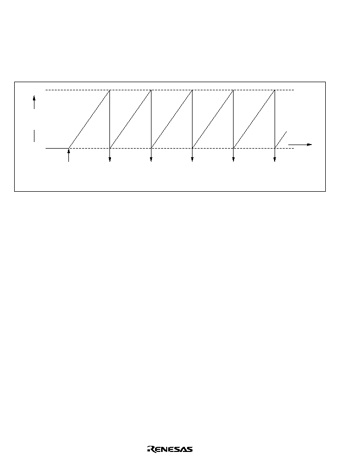
448
12.3.2
Interval Timer Operation
Figure 12.5 illustrates interval timer operation. To use the WDT as an interval timer, clear bit
WT/
IT to 0 and set bit TME to 1 in TCSR. An interval timer interrupt request is generated at each
TCNT overflow. This function can be used to generate interval timer interrupts at regular
intervals.
TCNT
count value
Time t
Interval
timer
interrupt
Interval
timer
interrupt
Interval
timer
interrupt
Interval
timer
interrupt
WT/ = 0
TME = 1
IT
H'FF
H'00
Figure 12.5 Interval Timer Operation
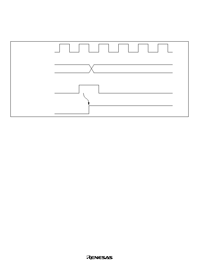
449
12.3.3
Timing of Setting of Overflow Flag (OVF)
Figure 12.6 shows the timing of setting of the OVF flag. The OVF flag is set to 1 when TCNT
overflows. At the same time, a reset signal is generated in watchdog timer operation, or an interval
timer interrupt is generated in interval timer operation.
TCNT
Overflow signal
OVF
H'FF
H'00
Figure 12.6 Timing of Setting of OVF
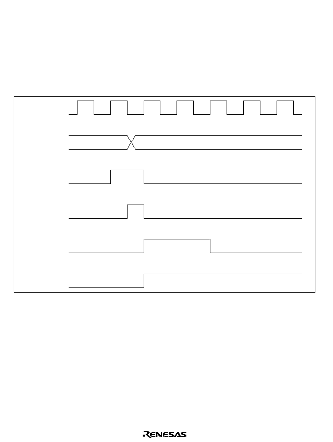
450
12.3.4
Timing of Setting of Watchdog Timer Reset Bit (WRST)
The WRST bit in RSTCSR is valid when bits WT/
IT and TME are both set to 1 in TCSR.
Figure 12.7 shows the timing of setting of WRST and the internal reset timing. The WRST bit is
set to 1 when TCNT overflows and OVF is set to 1. At the same time an internal reset signal is
generated for the entire H8/3069F chip. This internal reset signal clears OVF to 0, but the WRST
bit remains set to 1. The reset routine must therefore clear the WRST bit.
TCNT
Overflow signal
OVF
WRST
H'FF
H'00
WDT internal
reset
Figure 12.7 Timing of Setting of WRST Bit and Internal Reset
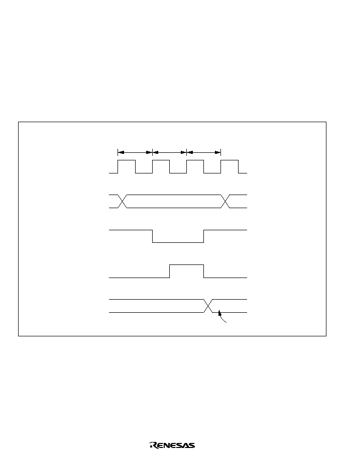
451
12.4
Interrupts
During interval timer operation, an overflow generates an interval timer interrupt (WOVI). The
interval timer interrupt is requested whenever the OVF bit is set to 1 in TCSR.
12.5
Usage Notes
Contention between TCNT Write and Increment: If a timer counter clock pulse is generated
during the T
3
state of a write cycle to TCNT, the write takes priority and the timer count is not
incremented. See figure 12.8.
TCNT
TCNT
N
M
Counter write data
T
3
T
2
T
1
CPU: TCNT write cycle
Internal write
signal
TCNT input
clock
Figure 12.8 Contention between TCNT Write and Count up
Changing CKS2 to CKS0 Bit: Halt TCNT by clearing the TME bit to 0 in TCSR before
changing the values of bits CKS2 to CKS0.

452

453
Section 13 Serial Communication Interface
13.1
Overview
The H8/3069F has a serial communication interface (SCI) with three independent channels. All
three channels have identical functions. The SCI can communicate in both asynchronous and
synchronous mode. It also has a multiprocessor communication function for serial communication
among two or more processors.
When the SCI is not used, it can be halted to conserve power. Each SCI channel can be halted
independently. For details, see section 20.6, Module Standby Function.
The SCI also has a smart card interface function conforming to the ISO/IEC 7816-3 (Identification
Card) standard. This function supports serial communication with a smart card. Switching
between the normal serial communication interface and the smart card interface is carried out by
means of a register setting.
13.1.1
Features
SCI features are listed below.
�
Selection of synchronous or asynchronous mode for serial communication
Asynchronous mode
Serial data communication is synchronized one channel at a time. The SCI can communicate
with a universal asynchronous receiver/transmitter (UART), asynchronous communication
interface adapter (ACIA), or other chip that employs standard asynchronous communication.
It can also communicate with two or more other processors using the multiprocessor
communication function. There are 12 selectable serial data transfer formats.
Data length:
7 or 8 bits
Stop bit length:
1 or 2 bits
Parity:
even/odd/none
Multiprocessor bit:
1 or 0
Receive error detection:
parity, overrun, and framing errors
Break detection:
by reading the RxD level directly when a framing error occurs
Synchronous mode
Serial data communication is synchronized with a clock signal. The SCI can communicate
with other chips having a synchronous communication function.
There is a single serial data communication format.
Data length:
8 bits
Receive error detection:
overrun errors

454
�
Full-duplex communication
The transmitting and receiving sections are independent, so the SCI can transmit and receive
simultaneously. The transmitting and receiving sections are both double-buffered, so serial
data can be transmitted and received continuously.
�
The following settings can be made for the serial data to be transferred:
LSB-first or MSB-first transfer
Inversion of data logic level
�
Built-in baud rate generator with selectable bit rates
�
Selectable transmit/receive clock sources: internal clock from baud rate generator, or external
clock from the SCK pin
�
Four types of interrupts
Transmit-data-empty, transmit-end, receive-data-full, and receive-error interrupts are requested
independently. The transmit-data-empty and receive-data-full interrupts from SCI0 can
activate the DMA controller (DMAC) to transfer data.
Features of the smart card interface are listed below.
�
Asynchronous communication
Data length: 8 bits
Parity bits generated and checked
Error signal output in receive mode (parity error)
Error signal detect and automatic data retransmit in transmit mode
Supports both direct convention and inverse convention
�
Built-in baud rate generator with selectable bit rates
�
Three types of interrupts
Transmit-data-empty, receive-data-full, and transmit/receive-error interrupts are requested
independently. The transmit-data-empty and receive-data-full interrupts can activate the DMA
controller (DMAC) to transfer data.
455
13.1.2
Block Diagram
Figure 13.1 shows a block diagram of the SCI.
RDR
RSR
TDR
TSR
SSR
SCR
SMR
SCMR
BRR
/ 4
/16
/64
RxD
TxD
SCK
T E I
T X I
R X I
E R I
Legend
RSR
: Receive shift register
RDR
: Receive data register
TSR
: Transmit shift register
TDR
: Transmit data register
SMR
: Serial mode register
SCR
: Serial control register
SSR
: Serial status register
BRR
: Bit rate register
SCMR : Smart card mode register
Module data bus
Bus interface
Internal data bus
Parity generate
Parity check
Transmit/receive
control
Baud rate
generator
Clock
External clock
Figure 13.1 SCI Block Diagram

456
13.1.3
Input/Output Pins
The SCI has serial pins for each channel as listed in table 13.1.
Table 13.1
SCI Pins
Channel Name
Abbreviation
I/O
Function
0
Serial clock pin
SCK
0
Input/output
SCI
0
clock input/output
Receive data pin
RxD
0
Input
SCI
0
receive data input
Transmit data pin
TxD
0
Output
SCI
0
transmit data output
1
Serial clock pin
SCK
1
Input/output
SCI
1
clock input/output
Receive data pin
RxD
1
Input
SCI
1
receive data input
Transmit data pin
TxD
1
Output
SCI
1
transmit data output
2
Serial clock pin
SCK
2
Input/output
SCI
2
clock input/output
Receive data pin
RxD
2
Input
SCI
2
receive data input
Transmit data pin
TxD
2
Output
SCI
2
transmit data output

457
13.1.4
Register Configuration
The SCI has internal registers as listed in table 13.2. These registers select asynchronous or
synchronous mode, specify the data format and bit rate, control the transmitter and receiver
sections, and specify switching between the serial communication interface and smart card
interface.
Table 13.2
SCI Registers
Channel
Address
*
1
Name
Abbreviation
R/W
Initial Value
0
H'FFFB0
Serial mode register
SMR
R/W
H'00
H'FFFB1
Bit rate register
BRR
R/W
H'FF
H'FFFB2
Serial control register
SCR
R/W
H'00
H'FFFB3
Transmit data register
TDR
R/W
H'FF
H'FFFB4
Serial status register
SSR
R/(W)
*
2
H'84
H'FFFB5
Receive data register
RDR
R
H'00
H'FFFB6
Smart card mode register
SCMR
R/W
H'F2
1
H'FFFB8
Serial mode register
SMR
R/W
H'00
H'FFFB9
Bit rate register
BRR
R/W
H'FF
H'FFFBA
Serial control register
SCR
R/W
H'00
H'FFFBB
Transmit data register
TDR
R/W
H'FF
H'FFFBC
Serial status register
SSR
R/(W)
*
2
H'84
H'FFFBD
Receive data register
RDR
R
H'00
H'FFFBE
Smart card mode register
SCMR
R/W
H'F2
2
H'FFFC0
Serial mode register
SMR
R/W
H'00
H'FFFC1
Bit rate register
BRR
R/W
H'FF
H'FFFC2
Serial control register
SCR
R/W
H'00
H'FFFC3
Transmit data register
TDR
R/W
H'FF
H'FFFC4
Serial status register
SSR
R/(W)
*
2
H'84
H'FFFC5
Receive data register
RDR
R
H'00
H'FFFC6
Smart card mode register
SCMR
R/W
H'F2
Notes:
*
1 Indicates the lower 20 bits of the address in advanced mode.
*
2 Only 0 can be written, to clear flags.

458
13.2
Register Descriptions
13.2.1
Receive Shift Register (RSR)
RSR is the register that receives serial data.
Bit
7
6
5
4
3
2
1
0
Read/Write
The SCI loads serial data input at the RxD pin into RSR in the order received, LSB (bit 0) first,
thereby converting the data to parallel data. When one byte of data has been received, it is
automatically transferred to RDR. The CPU cannot read or write RSR directly.
13.2.2
Receive Data Register (RDR)
RDR is the register that stores received serial data.
Bit
7
6
5
4
3
2
1
0
Initial value
Read/Write
R
0
0
0
0
0
0
0
0
R
R
R
R
R
R
R
When the SCI has received one byte of serial data, it transfers the received data from RSR into
RDR for storage, completing the receive operation. RSR is then ready to receive the next data.
This double-buffering allows data to be received continuously.
RDR is a read-only register. Its contents cannot be modified by the CPU. RDR is initialized to
H'00 by a reset and in standby mode.

459
13.2.3
Transmit Shift Register (TSR)
TSR is the register that transmits serial data.
Bit
7
6
5
4
3
2
1
0
Read/Write
The SCI loads transmit data from TDR to TSR, then transmits the data serially from the TxD pin,
LSB (bit 0) first. After transmitting one data byte, the SCI automatically loads the next transmit
data from TDR into TSR and starts transmitting it. If the TDRE flag is set to 1 in SSR, however,
the SCI does not load the TDR contents into TSR. The CPU cannot read or write RSR directly.
13.2.4
Transmit Data Register (TDR)
TDR is an 8-bit register that stores data for serial transmission.
Bit
7
6
5
4
3
2
1
0
Initial value
Read/Write
R/W
1
1
1
1
1
1
1
1
R/W
R/W
R/W
R/W
R/W
R/W
R/W
When the SCI detects that TSR is empty, it moves transmit data written in TDR from TDR into
TSR and starts serial transmission. Continuous serial transmission is possible by writing the next
transmit data in TDR during serial transmission from TSR.
The CPU can always read and write TDR. TDR is initialized to H'FF by a reset and in standby
mode.

460
13.2.5
Serial Mode Register (SMR)
SMR is an 8-bit register that specifies the SCI's serial communication format and selects the clock
source for the baud rate generator.
C/
A
CHR
PE
O/
E
STOP
MP
CKS1
CKS0
R/W
0
0
0
0
0
0
0
0
R/W
R/W
R/W
R/W
R/W
R/W
R/W
Initial value
Read/Write
Bit
7
6
5
4
3
2
1
0
Clock select 1/0
These bits select the
baud rate generator's
clock source
Communication mode
Selects asynchronous or synchronous mode
Character length
Selects character length in asynchronous mode
Parity enable
Enables or disables the addition of a parity bit
Parity mode
Selects even or odd parity
Stop bit length
Selects the stop bit length
Multiprocessor mode
Selects the multiprocessor
function
The CPU can always read and write SMR. SMR is initialized to H'00 by a reset and in standby
mode.
Bit 7--Communication Mode (C/
A)/GSM Mode (GM): The function of this bit differs for the
normal serial communication interface and for the smart card interface. Its function is switched
with the SMIF bit in SCMR.

461
For serial communication interface (SMIF bit in SCMR cleared to 0): Selects whether the SCI
operates in asynchronous or synchronous mode.
Bit 7
C/
A
Description
0
Asynchronous mode
(Initial value)
1
Synchronous mode
For smart card interface (SMIF bit in SCMR set to 1): Selects GSM mode for the smart card
interface.
Bit 7
GM
Description
0
The TEND flag is set 12.5 etu after the start bit
(Initial value)
1
The TEND flag is set 11.0 etu after the start bit
Note:
etu: Elementary time unit (time required to transmit one bit)
Bit 6--Character Length (CHR): Selects 7-bit or 8-bits data length in asynchronous mode. In
synchronous mode, the data length is 8 bits regardless of the CHR setting,
Bit 6
CHR
Description
0
8-bit data
(Initial value)
1
7-bit data
*
Note:
*
When 7-bit data is selected, the MSB (bit 7) of TDR is not transmitted.
Bit 5--Parity Enable (PE): In asynchronous mode, this bit enables or disables the addition of a
parity bit to transmit data, and the checking of the parity bit in receive data. In synchronous mode,
the parity bit is neither added nor checked, regardless of the PE bit setting.
Bit 5
PE
Description
0
Parity bit not added or checked
(Initial value)
1
Parity bit added and checked
*
Note:
*
When PE bit is set to 1, an even or odd parity bit is added to transmit data according to the
even or odd parity mode selection by the O/
E
bit, and the parity bit in receive data is
checked to see that it matches the even or odd mode selected by the O/
E
bit.

462
Bit 4--Parity Mode (O/
E): Selects even or odd parity. The O/E bit setting is only valid when the
PE bit is set to 1, enabling parity bit addition and checking, in asynchronous mode. The O/
E bit
setting is ignored in synchronous mode, or when parity addition and checking is disabled in
asynchronous mode.
Bit 4
O/
E
Description
0
Even parity
*
1
(Initial value)
1
Odd parity
*
2
Notes:
*
1 When even parity is selected, the parity bit added to transmit data makes an even
number of 1s in the transmitted character and parity bit combined. Receive data must
have an even number of 1s in the received character and parity bit combined.
*
2 When odd parity is selected, the parity bit added to transmit data makes an odd number
of 1s in the transmitted character and parity bit combined. Receive data must have an
odd number of 1s in the received character and parity bit combined.
Bit 3--Stop Bit Length (STOP): Selects one or two stop bits in asynchronous mode. This setting
is used only in asynchronous mode. In synchronous mode no stop bit is added, so the STOP bit
setting is ignored.
Bit 3
STOP
Description
0
1 stop bit
*
1
(Initial value)
1
2 stop bits
*
2
Notes:
*
1 One stop bit (with value 1) is added to the end of each transmitted character.
*
2 Two stop bits (with value 1) are added to the end of each transmitted character.
In receiving, only the first stop bit is checked, regardless of the STOP bit setting. If the second
stop bit is 1, it is treated as a stop bit. If the second stop bit is 0, it is treated as the start bit of the
next incoming character.
Bit 2--Multiprocessor Mode (MP): Selects a multiprocessor format. When a multiprocessor
format is selected, parity settings made by the PE and O/
E bits are ignored. The MP bit setting is
valid only in asynchronous mode. It is ignored in synchronous mode.
For further information on the multiprocessor communication function, see section 13.3.3,
Multiprocessor Communication.
Bit 2
MP
Description
0
Multiprocessor function disabled
(Initial value)
1
Multiprocessor format selected

463
Bits 1 and 0--Clock Select 1 and 0 (CKS1/0): These bits select the clock source for the on-chip
baud rate generator. Four clock sources are available:
,
/4,
/16, and
/64.
For the relationship between the clock source, bit rate register setting, and baud rate, see section
13.2.8, Bit Rate Register (BRR).
Bit 1
CKS1
Bit 0
CKS0
Description
0
0
(Initial value)
0
1
/4
1
0
/16
1
1
/64
464
13.2.6
Serial Control Register (SCR)
SCR register enables or disables the SCI transmitter and receiver, enables or disables serial clock
output in asynchronous mode, enables or disables interrupts, and selects the transmit/receive clock
source.
Bit 7
6
5
4
3
2
1
0
TIE
RIE
TE
RE
MPIE
TEIE
CKE1
CKE0
Initial value
Read/Write
R/W
0
0
0
0
0
0
0
0
R/W
R/W
R/W
R/W
R/W
R/W
R/W
Transmit-end interrupt enable
Enables or disables transmit-end
interrupts (TEI)
Multiprocessor interrupt enable
Enables or disables multiprocessor
interrupts
Receive enable
Enables or disables the receiver
Transmit enable
Enables or disables the transmitter
Receive interrupt enable
Enables or disables receive-data-full interrupts (RXI) and
receive-error interrupts (ERI)
Transmit interrupt enable
Enables or disables transmit-data-empty interrupts (TXI)
Clock enable 1/0
These bits select the
SCI clock source
The CPU can always read and write SCR. SCR is initialized to H'00 by a reset and in standby
mode.

465
Bit 7--Transmit Interrupt Enable (TIE): Enables or disables the transmit-data-empty interrupt
(TXI) requested when the TDRE flag in SSR is set to 1 due to transfer of serial transmit data from
TDR to TSR.
Bit 7
TIE
Description
0
Transmit-data-empty interrupt request (TXI) is disabled
*
(Initial value)
1
Transmit-data-empty interrupt request (TXI) is enabled
Note:
*
TXI interrupt requests can be cleared by reading the value 1 from the TDRE flag, then
clearing it to 0; or by clearing the TIE bit to 0.
Bit 6--Receive Interrupt Enable (RIE): Enables or disables the receive-data-full interrupt (RXI)
requested when the RDRF flag in SSR is set to 1 due to transfer of serial receive data from RSR to
RDR; also enables or disables the receive-error interrupt (ERI).
Bit 6
RIE
Description
0
Receive-data-full (RXI) and receive-error (ERI) interrupt requests are disabled
*
(Initial value)
1
Receive-data-full (RXI) and receive-error (ERI) interrupt requests are enabled
Note:
*
RXI and ERI interrupt requests can be cleared by reading the value 1 from the RDRF, FER,
PER, or ORER flag, then clearing the flag to 0; or by clearing the RIE bit to 0.
Bit 5--Transmit Enable (TE): Enables or disables the start of SCI serial transmitting operations.
Bit 5
TE
Description
0
Transmitting disabled
*
1
(Initial value)
1
Transmitting enabled
*
2
Notes:
*
1 The TDRE flag is fixed at 1 in SSR.
*
2 In the enabled state, serial transmission starts when the TDRE flag in SSR is cleared to
0 after writing of transmit data into TDR. Select the transmit format in SMR before
setting the TE bit to 1.

466
Bit 4--Receive Enable (RE): Enables or disables the start of SCI serial receiving operations.
Bit 4
RE
Description
0
Receiving disabled
*
1
(Initial value)
1
Receiving enabled
*
2
Notes:
*
1 Clearing the RE bit to 0 does not affect the RDRF, FER, PER, and ORER flags. These
flags retain their previous values.
*
2 In the enabled state, serial receiving starts when a start bit is detected in asynchronous
mode, or serial clock input is detected in synchronous mode. Select the receive format
in SMR before setting the RE bit to 1.
Bit 3--Multiprocessor Interrupt Enable (MPIE): Enables or disables multiprocessor interrupts.
The MPIE bit setting is valid only in asynchronous mode, and only if the MP bit is set to 1 in
SMR. The MPIE bit setting is ignored in synchronous mode or when the MP bit is cleared to 0.
Bit 3
MPIE
Description
0
Multiprocessor interrupts are disabled (normal receive operation) (Initial value)
Clearing conditions
(1) The MPIE bit is cleared to 0
(2) MPB = 1 in received data
1
Multiprocessor interrupts are enabled
*
Receive-data-full interrupts (RXI), receive-error interrupts (ERI), and setting of
the RDRF, FER, and ORER status flags in SSR are disabled until data with the
multiprocessor bit set to 1 is received.
Note:
*
The SCI does not transfer receive data from RSR to RDR, does not detect receive errors,
and does not set the RDRF, FER, and ORER flags in SSR. When it receives data in which
MPB = 1, the SCI sets the MPB bit to 1 in SSR, automatically clears the MPIE bit to 0,
enables RXI and ERI interrupts (if the TIE and RIE bits in SCR are set to 1), and allows the
FER and ORER flags to be set.
Bit 2--Transmit-End interrupt Enable (TEIE): Enables or disables the transmit-end interrupt
(TEI) requested if TDR does not contain valid transmit data when the MSB is transmitted.
Bit 2
TEIE
Description
0
Transmit-end interrupt requests (TEI) are disabled
*
(Initial value)
1
Transmit-end interrupt requests (TEI) are enabled
*
Note:
*
TEI interrupt requests can be cleared by reading the value 1 from the TDRE flag in SSR,
then clearing the TDRE flag to 0, thereby also clearing the TEND flag to 0; or by clearing
the TEIE bit to 0.

467
Bits 1 and 0--Clock Enable 1 and 0 (CKE1/0): The function of these bits differs for the normal
serial communication interface and for the smart card interface. Their function is switched with
the SMIF bit in SCMR.
For serial communication interface (SMIF bit in SCMR cleared to 0): These bits select the
SCI clock source and enable or disable clock output from the SCK pin. Depending on the settings
of CKE1 and CKE0, the SCK pin can be used for generic input/output, serial clock output, or
serial clock input.
The CKE0 setting is valid only in asynchronous mode, and only when the SCI is internally
clocked (CKE1 = 0). The CKE0 setting is ignored in synchronous mode, or when an external
clock source is selected (CKE1 = 1). Select the SCI operating mode in SMR before setting the
CKE1 and CKE0 bits . For further details on selection of the SCI clock source, see table 13.9 in
section 13.3, Operation.
Bit 1
CKE1
Bit 0
CKE0 Description
0
0
Asynchronous mode
Internal clock, SCK pin available for generic input/output
*
1
Synchronous mode
Internal clock, SCK pin used for serial clock output
*
1
0
1
Asynchronous mode
Internal clock, SCK pin used for clock output
*
2
Synchronous mode
Internal clock, SCK pin used for serial clock output
1
0
Asynchronous mode
External clock, SCK pin used for clock input
*
3
Synchronous mode
External clock, SCK pin used for serial clock input
1
1
Asynchronous mode
External clock, SCK pin used for clock input
*
3
Synchronous mode
External clock, SCK pin used for serial clock input
Notes:
*
1 Initial value
*
2 The output clock frequency is the same as the bit rate.
*
3 The input clock frequency is 16 times the bit rate.

468
For smart card interface (SMIF bit in SCMR set to 1): These bits, together with the GM bit in
SMR, determine whether the SCK pin is used for generic input/output or as the serial clock output
pin.
SMR
GM
Bit 1
CKE1
Bit 0
CKE0 Description
0
0
0
SCK pin available for generic input/output
(Initial value)
0
0
1
SCK pin used for clock output
1
0
0
SCK pin output fixed low
1
0
1
SCK pin used for clock output
1
1
0
SCK pin output fixed high
1
1
1
SCK pin used for clock output

469
13.2.7
Serial Status Register (SSR)
SSR is an 8-bit register containing multiprocessor bit values, and status flags that indicate the
operating status of the SCI.
Initial value
Read/Write
R
R/W
0
1
0
0
0
1
0
0
Bit
7
6
5
4
3
2
1
0
Multiprocessor bit
transfer
Value of multiprocessor
bit to be transmitted
R/(W)
*
1
R/(W)
*
1
R/(W)
*
1
R/(W)
*
1
R/(W)
*
1
R
TDRE
RDRF
ORER
FER/ERS
PER
TEND
MPB
MPBT
Multiprocessor bit
Stores the received
multiprocessor bit value
Transmit end
*
2
Status flag indicating end of
transmission
Parity error
Status flag indicating detection
of a receive parity error
Framing error (FER)/Error signal status (ERS)
*
2
Status flag indicating detection of a receive framing
error, or flag indicating detection of an error signal
Overrun error
Status flag indicating detection
of a receive overrun error
Receive data register full
Status flag indicating that data has been received
and stored in RDR
Transmit data register empty
Status flag indicating that transmit data has been transferred from
TDR into TSR and new data can be written in TDR
Notes:
*
1 Only 0 can be written, to clear the flag.
*
2 Function differs between the normal serial communication interface and the smart card interface.
The CPU can always read and write SSR, but cannot write 1 in the TDRE, RDRF, ORER, PER,
and FER flags. These flags can be cleared to 0 only if they have first been read while set to 1.
The TEND and MPB flags are read-only bits that cannot be written.
SSR is initialized to H'84 by a reset and in standby mode.

470
Bit 7--Transmit Data Register Empty (TDRE): Indicates that the SCI has loaded transmit data
from TDR into TSR and the next serial data can be written in TDR.
Bit 7
TDRE
Description
0
TDR contains valid transmit data
[Clearing conditions]
Read TDRE when TDRE = 1, then write 0 in TDRE
The DMAC writes data in TDR
1
TDR does not contain valid transmit data
(Initial value)
[Setting conditions]
The chip is reset or enters standby mode
The TE bit in SCR is cleared to 0
TDR contents are loaded into TSR, so new data can be written in TDR
Bit 6--Receive Data Register Full (RDRF): Indicates that RDR contains new receive data.
Bit 6
RDRF
Description
0
RDR does not contain new receive data
(Initial value)
[Clearing conditions]
The chip is reset or enters standby mode
Read RDRF when RDRF = 1, then write 0 in RDRF
The DMAC reads data from RDR
1
RDR contains new receive data
[Setting condition]
Serial data is received normally and transferred from RSR to RDR
Note:
The RDR contents and the RDRF flag are not affected by detection of receive errors or by
clearing of the RE bit to 0 in SCR. They retain their previous values. If the RDRF flag is
still set to 1 when reception of the next data ends, an overrun error will occur and the
receive data will be lost.

471
Bit 5--Overrun Error (ORER): Indicates that data reception ended abnormally due to an
overrun error.
Bit 5
ORER
Description
0
Receiving is in progress or has ended normally
*
1
(Initial value)
[Clearing conditions]
The chip is reset or enters standby mode
Read ORER when ORER = 1, then write 0 in ORER
1
A receive overrun error occurred
*
2
[Setting condition]
Reception of the next serial data ends when RDRF = 1
Notes:
*
1 Clearing the RE bit to 0 in SCR does not affect the ORER flag, which retains its
previous value.
*
2 RDR continues to hold the receive data prior to the overrun error, so subsequent
receive data is lost. Serial receiving cannot continue while the ORER flag is set to 1. In
synchronous mode, serial transmitting is also disabled.
Bit 4--Framing Error (FER)/Error Signal Status (ERS): The function of this bit differs for the
normal serial communication interface and for the smart card interface. Its function is switched
with the SMIF bit in SCMR.
For serial communication interface (SMIF bit in SCMR cleared to 0): Indicates that data
reception ended abnormally due to a framing error in asynchronous mode.
Bit 4
FER
Description
0
Receiving is in progress or has ended normally
*
1
(Initial value)
[Clearing conditions]
The chip is reset or enters standby mode
Read FER when FER = 1, then write 0 in FER
1
A receive framing error occurred
*
2
[Setting condition]
The stop bit at the end of the receive data is checked and found to be 0
Notes:
*
1 Clearing the RE bit to 0 in SCR does not affect the FER flag, which retains its previous
value.
*
2 When the stop bit length is 2 bits, only the first bit is checked. The second stop bit is
not checked. When a framing error occurs the SCI transfers the receive data into RDR
but does not set the RDRF flag. Serial receiving cannot continue while the FER flag is
set to 1. In synchronous mode, serial transmitting is also disabled.

472
For smart card interface (SMIF bit in SCMR set to 1): Indicates the status of the error signal
sent back from the receiving side during transmission. Framing errors are not detected in smart
card interface mode.
Bit 4
ERS
Description
0
Normal reception, no error signal
*
(Initial value)
[Clearing conditions]
The chip is reset or enters standby mode
Read ERS when ERS = 1, then write 0 in ERS
1
An error signal has been sent from the receiving side indicating detection of a
parity error
[Setting condition]
The error signal is low when sampled
Note:
*
Clearing the TE bit to 0 in SCR does not affect the ERS flag, which retains its previous
value.
Bit 3--Parity Error (PER): Indicates that data reception ended abnormally due to a parity error
in asynchronous mode.
Bit 3
PER
Description
0
Receiving is in progress or has ended normally
*
1
(Initial value)
[Clearing conditions]
The chip is reset or enters standby mode
Read PER when PER = 1, then write 0 in PER
1
A receive parity error occurred
*
2
[Setting condition]
The number of 1s in receive data, including the parity bit, does not match the
even or odd parity setting of O/
E
in SMR
Notes:
*
1 Clearing the RE bit to 0 in SCR does not affect the PER flag, which retains its previous
value.
*
2 When a parity error occurs the SCI transfers the receive data into RDR but does not set
the RDRF flag. Serial receiving cannot continue while the PER flag is set to 1. In
synchronous mode, serial transmitting is also disabled.
Bit 2--Transmit End (TEND): The function of this bit differs for the normal serial
communication interface and for the smart card interface. Its function is switched with the SMIF
bit in SCMR.
For serial communication interface (SMIF bit in SCMR cleared to 0): Indicates that when the
last bit of a serial character was transmitted TDR did not contain valid transmit data, so
transmission has ended. The TEND flag is a read-only bit and cannot be written.

473
Bit 2
TEND
Description
0
Transmission is in progress
[Clearing conditions]
Read TDRE when TDRE = 1, then write 0 in TDRE
The DMAC writes data in TDR
1
End of transmission
(Initial value)
[Setting conditions]
The chip is reset or enters standby mode
The TE bit in SCR is cleared to 0
TDRE is 1 when the last bit of a 1-byte serial transmit character is transmitted
For smart card interface (SMIF bit in SCMR set to 1): Indicates that when the last bit of a
serial character was transmitted TDR did not contain valid transmit data, so transmission has
ended. The TEND flag is a read-only bit and cannot be written.
Bit 2
TEND
Description
0
Transmission is in progress
[Clearing conditions]
Read TDRE when TDRE = 1, then write 0 in TDRE
The DMAC writes data in TDR
1
End of transmission
(Initial value)
[Setting conditions]
The chip is reset or enters standby mode
The TE bit is cleared to 0 in SCR and the FER/ERS bit is also cleared to 0
TDRE is 1 and FER/ERS is 0 (normal transmission) 2.5 etu (when GM = 0) or
1.0 etu (when GM = 1) after a 1-byte serial character is transmitted
Note:
etu: Elementary time unit (time required to transmit one bit)
Bit 1--Multiprocessor bit (MPB): Stores the value of the multiprocessor bit in the receive data
when a multiprocessor format is used in asynchronous mode. MPB is a read-only bit, and cannot
be written.
Bit 1
MPB
Description
0
Multiprocessor bit value in receive data is 0
*
(Initial value)
1
Multiprocessor bit value in receive data is 1
Note:
*
If the RE bit in SCR is cleared to 0 when a multiprocessor format is selected, MPB retains
its previous value.

474
Bit 0--Multiprocessor Bit Transfer (MPBT): Stores the value of the multiprocessor bit added to
transmit data when a multiprocessor format in selected for transmitting in asynchronous mode.
The MPBT bit setting is ignored in synchronous mode, when a multiprocessor format is not
selected, or when the SCI cannot transmit.
Bit 1
MPBT
Description
0
Multiprocessor bit value in transmit data is 0
(Initial value)
1
Multiprocessor bit value in transmit data is 1
13.2.8
Bit Rate Register (BRR)
BRR is an 8-bit register that., together with the CKS1 and CKS0 bits in SMR that select the baud
rate generator clock source, determines the serial communication bit rate.
Bit
Initial value
Read/Write
7
R/W
R/W
R/W
R/W
R/W
R/W
R/W
R/W
6
1
1
1
1
1
1
1
1
5
4
3
2
1
0
The CPU can always read and write BRR. BRR is initialized to H'FF by a reset and in standby
mode. Each SCI channel has independent baud rate generator control, so different values can be
set in the three channels.
Table 13.3 shows examples of BRR settings in asynchronous mode. Table 13.4 shows examples
of BRR settings in synchronous mode.

475
Table 13.3
Examples of Bit Rates and BRR Settings in Asynchronous Mode
(MHz)
Bit Rate
2
2.097152
2.4576
3
(bit/s)
n
N
Error (%) n
N
Error (%) n
N
Error (%) n
N
Error (%)
110
1
141 0.03
1
148 �0.04
1
174 �0.26
1
212 0.03
150
1
103 0.16
1
108 0.21
1
127 0.00
1
155 0.16
300
0
207 0.16
0
217 0.21
0
255 0.00
1
77
0.16
600
0
103 0.16
0
108 0.21
0
127 0.00
0
155 0.16
1200
0
51
0.16
0
54
�0.70
0
63
0.00
0
77
0.16
2400
0
25
0.16
0
26
1.14
0
31
0.00
0
38
0.16
4800
0
12
0.16
0
13
�2.48
0
15
0.00
0
19
�2.34
9600
0
6
�6.99
0
6
�2.48
0
7
0.00
0
9
�2.34
19200
0
2
8.51
0
2
13.78
0
3
0.00
0
4
�2.34
31250
0
1
0.00
0
1
4.86
0
1
22.88
0
2
0.00
38400
0
1
�18.62
0
1
�14.67
0
1
0.00
--
--
--
(MHz)
Bit Rate
3.6864
4
4.9152
5
(bit/s)
n
N
Error (%) n
N
Error (%) n
N
Error (%) n
N
Error (%)
110
2
64
0.70
2
70
0.03
2
86
0.31
2
88
�0.25
150
1
191 0.00
1
207 0.16
1
255 0.00
2
64
0.16
300
1
95
0.00
1
103 0.16
1
127 0.00
1
129 0.16
600
0
191 0.00
0
207 0.16
0
255 0.00
1
64
0.16
1200
0
95
0.00
0
103 0.16
0
127 0.00
0
129 0.16
2400
0
47
0.00
0
51
0.16
0
63
0.00
0
64
0.16
4800
0
23
0.00
0
25
0.16
0
31
0.00
0
32
�1.36
9600
0
11
0.00
0
12
0.16
0
15
0.00
0
15
1.73
19200
0
5
0.00
0
6
�6.99
0
7
0.00
0
7
1.73
31250
--
--
--
0
3
0.00
0
4
�1.70
0
4
0.00
38400
0
2
0.00
0
2
8.51
0
3
0.00
0
3
1.73

476
(MHz)
Bit Rate
6
6.144
7.3728
8
(bit/s)
n
N
Error (%) n
N
Error (%) n
N
Error (%) n
N
Error (%)
110
2
106 �0.44
2
108 0.08
2
130 �0.07
2
141 0.03
150
2
77
0.16
2
79
0.00
2
95
0.00
2
103 0.16
300
1
155 0.16
1
159 0.00
1
191 0.00
1
207 0.16
600
1
77
0.16
1
79
0.00
1
95
0.00
1
103 0.16
1200
0
155 0.16
0
159 0.00
0
191 0.00
0
207 0.16
2400
0
77
0.16
0
79
0.00
0
95
0.00
0
103 0.16
4800
0
38
0.16
0
39
0.00
0
47
0.00
0
51
0.16
9600
0
19
�2.34
0
19
0.00
0
23
0.00
0
25
0.16
19200
0
9
�2.34
0
9
0.00
0
11
0.00
0
12
0.16
31250
0
5
0.00
0
5
2.40
0
6
5.33
0
7
0.00
38400
0
4
�2.34
0
4
0.00
0
5
0.00
0
6
�6.99
(MHz)
Bit Rate
9.8304
10
12
12.288
(bit/s)
n
N
Error (%) n
N
Error (%) n
N
Error (%) n
N
Error (%)
110
2
174 �0.26
2
177 �0.25
2
212 0.03
2
217 0.08
150
2
127 0.00
2
129 0.16
2
155 0.16
2
159 0.00
300
1
255 0.00
2
64
0.16
2
77
0.16
2
79
0.00
600
1
127 0.00
1
129 0.16
1
155 0.16
1
159 0.00
1200
0
255 0.00
1
64
0.16
1
77
0.16
1
79
0.00
2400
0
127 0.00
0
129 0.16
0
155 0.16
0
159 0.00
4800
0
63
0.00
0
64
0.16
0
77
0.16
0
79
0.00
9600
0
31
0.00
0
32
�1.36
0
38
0.16
0
39
0.00
19200
0
15
0.00
0
15
1.73
0
19
�2.34
0
19
0.00
31250
0
9
�1.70
0
9
0.00
0
11
0.00
0
11
2.40
38400
0
7
0.00
0
7
1.73
0
9
�2.34
0
9
0.00

477
(MHz)
Bit
13
14
14.7456
16
18
20
25
Rate
(bit/s)
n N
Erro
r (%)
n N
Erro
r (%)
n N
Erro
r (%)
n N
Erro
r (%)
n N
Erro
r (%)
n N
Erro
r (%)
n N
Erro
r (%)
110
2 230 �
0.08
2 248 �
0.17
3 64
0.70 3 70
0.03 3 79
�
0.12
3 88
�
0.25
3 110 �
0.02
150
2 168 0.16 2 181 0.16 2 191 0.00 2 207 0.16 2 233 0.16 3 64
0.16 3 80
�
0.47
300
2 84
�
0.43
2 90
0.16 2 95
0.00 2 103 0.16 2 116 0.16 2 129 0.16 2 162 0.15
600
1 168 0.16 1 181 0.16 1 191 0.00 1 207 0.16 1 233 0.16 2 64
0.16 2 80
�
0.47
1200
1 84
�
0.43
1 90
0.16 1 95
0.00 1 103 0.16 1 116 0.16 1 129 0.16 1 162 0.15
2400
0 168 0.16 0 181 0.16 0 191 0.00 0 207 0.16 0 233 0.16 1 64
0.16 1 80
�
0.47
4800
0 84
�
0.43
0 90
0.16 0 95
0.00 0 103 0.16 0 116 0.16 0 129 0.16 0 162 0.15
9600
0 41
0.76 0 45
�
0.93
0 47
0.00 0 51
0.16 0 58
�
0.69
0 64
0.16 0 80
�
0.47
19200
0 20
0.76 0 22
�
0.93
0 23
0.00 0 25
0.16 0 28
1.02 0 32
�
1.36
0 40
�
0.76
31250
0 12
0.00 0 13
0.00 0 14
�
1.70
0 15
0.00 0 17
0.00 0 19
0.00 0 24
0.00
38400
0 10
�
3.82
0 10
3.57 0 11
0.00 0 12
0.16 0 14
�
2.34
0 15
1.73 0 19
1.73

478
Table 13.4
Examples of Bit Rates and BRR Settings in Synchronous Mode
Bit
(MHz)
Rate
2
4
8
10
13
16
18
20
25
(bit/s) n
N
n
N
n
N
n
N
n
N
n
N
n
N
n
N
n
N
110
3
70
--
--
--
--
--
--
--
--
--
--
--
--
--
--
--
--
250
2
124 2
249 3
124 --
--
3
202 3
249 --
--
--
--
--
--
500
1
249 2
124 2
249 --
--
3
101 3
124 3
140 3
155 --
--
1k
1
124 1
249 2
124 --
--
2
202 2
249 3
69
3
77
3
97
2.5k
0
199 1
99
1
199 1
249 2
80
2
99
2
112 2
124 2
155
5k
0
99
0
199 1
99
1
124 1
162 1
199 1
224 1
249 2
77
10k
0
49
0
99
0
199 0
249 1
80
1
99
1
112 1
124 1
155
25k
0
19
0
39
0
79
0
99
0
129 0
159 0
179 0
199 0
249
50k
0
9
0
19
0
39
0
49
0
64
0
79
0
89
0
99
0
124
100k
0
4
0
9
0
19
0
24
--
--
0
39
0
44
0
49
0
62
250k
0
1
0
3
0
7
0
9
0
12
0
15
0
17
0
19
0
24
500k
0
0
*
0
1
0
3
0
4
--
--
0
7
0
8
0
9
--
--
1M
0
0
*
0
1
--
--
--
--
0
3
0
4
0
4
--
--
2M
0
0
*
--
--
--
--
0
1
--
--
--
--
--
--
2.5M
--
--
0
0
*
--
--
--
--
--
--
--
--
--
--
4M
0
0
*
--
--
--
--
--
--
Note:
Settings with an error of 1% or less are recommended.
Legend
Blank : No setting available
-- :
Setting possible, but error occurs
*
:
Continuous transmission/reception not possible

479
The BRR setting is calculated as follows:
Asynchronous mode:
N =
64
�
2
2n�1
�
B
�
10
6
� 1
Synchronous mode:
N =
8
�
2
2n�1
�
B
�
10
6
� 1
B: Bit rate (bit/s)
N: BRR setting for baud rate generator (0
N
255)
: System clock frequency (MHz)
n: Baud rate generator clock source (n = 0, 1, 2, 3)
(For the clock sources and values of n, see the following table.)
SMR Settings
n
Clock Source
CKS1
CKS0
0
0
0
1
/4
0
1
2
/16
1
0
3
/64
1
1
The bit rate error in asynchronous mode is calculated as follows:
Error (%) =
(N + 1)
�
B
�
64
�
2
2n�1
� 1
�
100
�
10
6

480
Table 13.5 shows the maximum bit rates in asynchronous mode for various system clock
frequencies. Table 13.6 and 13.7 shows the maximum bit rates with external clock input.
Table 13.5
Maximum Bit Rates for Various Frequencies (Asynchronous Mode)
Settings
(MHz)
Maximum Bit Rate (bit/s)
n
N
2
62500
0
0
2.097152
65536
0
0
2.4576
76800
0
0
3
93750
0
0
3.6864
115200
0
0
4
125000
0
0
4.9152
153600
0
0
5
156250
0
0
6
187500
0
0
6.144
192000
0
0
7.3728
230400
0
0
8
250000
0
0
9.8304
307200
0
0
10
312500
0
0
12
375000
0
0
12.288
384000
0
0
14
437500
0
0
14.7456
460800
0
0
16
500000
0
0
17.2032
537600
0
0
18
562500
0
0
20
625000
0
0
25
781250
0
0

481
Table 13.6
Maximum Bit Rates with External Clock Input (Asynchronous Mode)
(MHz)
External Input Clock (MHz)
Maximum Bit Rate (bit/s)
2
0.5000
31250
2.097152
0.5243
32768
2.4576
0.6144
38400
3
0.7500
46875
3.6864
0.9216
57600
4
1.0000
62500
4.9152
1.2288
76800
5
1.2500
78125
6
1.5000
93750
6.144
1.5360
96000
7.3728
1.8432
115200
8
2.0000
125000
9.8304
2.4576
153600
10
2.5000
156250
12
3.0000
187500
12.288
3.0720
192000
14
3.5000
218750
14.7456
3.6864
230400
16
4.0000
250000
17.2032
4.3008
268800
18
4.5000
281250
20
5.0000
312500
25
6.2500
390625

482
Table 13.7
Maximum Bit Rates with External Clock Input (Synchronous Mode)
(MHz)
External Input Clock (MHz)
Maximum Bit Rate (bit/s)
2
0.3333
333333.3
4
0.6667
666666.7
6
1.0000
1000000.0
8
1.3333
1333333.3
10
1.6667
1666666.7
12
2.0000
2000000.0
14
2.3333
2333333.3
16
2.6667
2666666.7
18
3.0000
3000000.0
20
3.3333
3333333.3
25
4.1667
4166666.7

483
13.3
Operation
13.3.1
Overview
The SCI can carry out serial communication in two modes: asynchronous mode in which
synchronization is achieved character by character, and synchronous mode in which
synchronization is achieved with clock pulses. A smart card interface is also supported as a serial
communication function for an IC card interface.
Selection of asynchronous or synchronous mode and the transmission format for the normal serial
communication interface is made in SMR, as shown in table 13.8. The SCI clock source is
selected by the C/
A bit in SMR and the CKE1 and CKE0 bits in SCR, as shown in table 13.9.
For details of the procedures for switching between LSB-first and MSB-first mode and inverting
the data logic level, see section 14.2.1, Smart Card Mode Register (SCMR).
For selection of the smart card interface format, see section 14.3.3, Data Format.
Asynchronous Mode
�
Data length is selectable: 7 or 8 bits
�
Parity and multiprocessor bits are selectable, and so is the stop bit length (1 or 2 bits). These
selections determine the communication format and character length.
�
In receiving, it is possible to detect framing errors, parity errors, overrun errors, and the break
state.
�
An internal or external clock can be selected as the SCI clock source.
When an internal clock is selected, the SCI operates using the on-chip baud rate generator,
and can output a serial clock signal with a frequency matching the bit rate.
When an external clock is selected, the external clock input must have a frequency 16 times
the bit rate. (The on-chip baud rate generator is not used.)
Synchronous Mode
�
The communication format has a fixed 8-bit data length.
�
In receiving, it is possible to detect overrun errors.
�
An internal or external clock can be selected as the SCI clock source.
When an internal clock is selected, the SCI operates using the on-chip baud rate generator,
and can output a serial clock signal to external devices.
When an external clock is selected, the SCI operates on the input serial clock. The on-chip
baud rate generator is not used.

484
Smart Card Interface
�
One frame consists of 8-bit data and a parity bit.
�
In transmitting, a guard time of at least two elementary time units (2 etu) is provided between
the end of the parity bit and the start of he next frame. (An elementary time unit is the time
required to transmit one bit.)
�
In receiving, if a parity error is detected, a low error signal level is output for 1 etu, beginning
10.5 etu after the start bit.
�
In transmitting, if an error signal is received, the same data is automatically transmitted again
after at least 2 etu.
�
Only asynchronous communication is supported. There is no synchronous communication
function.
For details of smart card interface operation, see section 14, Smart Card Interface.
Table 13.8
SMR Settings and Serial Communication Formats
SMR Settings
SCI Communication Format
Bit 7
C/
A
Bit 6
CHR
Bit 2
MP
Bit 5
PE
Bit 3
STOP
Mode
Data
Length
Multi-
pro-
cessor
Bit
Parity
Bit
Stop Bit
Length
0
0
0
0
0
Asyn-
8-bit data
Absent
Absent
1 bit
1
chronous
2 bits
1
0
mode
Present
1 bit
1
2 bits
1
0
0
7-bit data
Absent
1 bit
1
2 bits
1
0
Present
1 bit
1
2 bits
0
1
--
0
Asyn-
chronous
8-bit data
Present
Absent
1 bit
--
1
mode (multi-
2 bits
1
--
0
processor
7-bit data
1 bit
--
1
format)
2 bits
1
--
--
--
--
Syn-
chronous
mode
8-bit data
Absent
None

485
Table 13.9
SMR and SCR Settings and SCI Clock Source Selection
SMR
SCR Setting
SCI Transmit/Receive clock
Bit 7
C/
A
Bit 1
CKE1
Bit 0
CKE0 Mode
Clock Source SCK Pin Function
0
0
0
Asynchronous
Internal
SCI does not use the SCK pin
1
mode
Outputs clock with frequency matching the
bit rate
1
0
External
Inputs clock with frequency 16 times the bit
1
rate
1
0
0
Synchronous
Internal
Outputs the serial clock
1
mode
1
0
External
Inputs the serial clock
1
13.3.2
Operation in Asynchronous Mode
In asynchronous mode, each transmitted or received character begins with a start bit and ends with
one or two stop bits. Serial communication is synchronized one character at a time.
The transmitting and receiving sections of the SCI are independent, so full-duplex communication
is possible. The transmitter and the receiver are both double-buffered, so data can be written and
read while transmitting and receiving are in progress, enabling continuous transmitting and
receiving.
Figure 13.2 shows the general format of asynchronous serial communication. In asynchronous
serial communication the communication line is normally held in the mark (high) state. The SCI
monitors the line and starts serial communication when the line goes to the space (low) state,
indicating a start bit. One serial character consists of a start bit (low), data (LSB first), parity bit
(high or low), and one or two stop bits (high), in that order.
When receiving in asynchronous mode, the SCI synchronizes at the falling edge of the start bit.
The SCI samples each data bit on the eighth pulse of a clock with a frequency 16 times the bit rate.
Receive data is latched at the center of each bit.

486
1
D0
D1
D2
D3
D4
D5
D6
D7
0/1
1
Idle (mark) state
1
(MSB)
(LSB)
0
1
Serial
data
Start
bit
1 bit
Transmit or receive data
7 or 8 bits
One unit of data (character or frame)
1 bit,
or
none
Parity
bit
1 or 2 bits
Stop bit(s)
Figure 13.2 Data Format in Asynchronous Communication
(Example: 8-Bit Data with Parity and 2 Stop Bits)
Communication Formats: Table 13.10 shows the 12 communication formats that can be selected
in asynchronous mode. The format is selected by settings in SMR.
487
Table 13.10 Serial Communication Formats (Asynchronous Mode)
7-bit data
STOP STOP
MPB
STOP
MPB
STOP
P
STOP
STOP
P
STOP STOP
SMR Settings
CHR
PE
MP
STOP
0
0
0
0
0
0
0
1
0
1
0
0
0
1
0
1
1
0
0
0
1
0
0
1
1
1
0
0
1
1
0
1
0
--
1
0
0
--
1
1
1
--
1
0
1
--
1
1
Serial Communication Format and Frame Length
1
2
3
4
5
6
7
8
9
10
11
12
STOP
8-bit data
S
8-bit data
S
STOP
P
8-bit data
S
8-bit data
S
STOP
7-bit data
S
7-bit data
S
7-bit data
S
S
8-bit data
S
STOP STOP
MPB
8-bit data
S
7-bit data
S
7-bit data
S
P
STOP
STOP
STOP
STOP
STOP
MPB
Legend
S:
Start bit
STOP: Stop bit
P:
Parity bit
MPB:
Multiprocessor bit
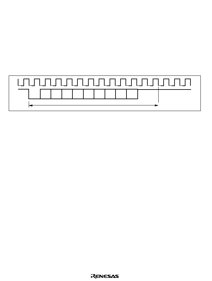
488
Clock: An internal clock generated by the on-chip baud rate generator or an external clock input
from the SCK pin can be selected as the SCI transmit/receive clock. The clock source is selected
by the C/
A bit in SMR and bits CKE1 and CKE0 in SCR. For details of SCI clock source
selection, see table 13.9.
When an external clock is input at the SCK pin, it must have a frequency 16 times the desired bit
rate.
When the SCI is operated on an internal clock, it can output a clock signal at the SCK pin. The
frequency of this output clock is equal to the bit rate. The phase is aligned as shown in figure 13.3
so that the rising edge of the clock occurs at the center of each transmit data bit.
D0
D1
D2
D3
D4
D5
D6
D7
0/1
1
1
0
1frame
Figure 13.3 Phase Relationship between Output Clock and Serial Data
(Asynchronous Mode)
Transmitting and Receiving Data:
�
SCI Initialization (Asynchronous Mode): Before transmitting or receiving data, clear the TE
and RE bits to 0 in SCR, then initialize the SCI as follows.
When changing the communication mode or format, always clear the TE and RE bits to 0
before following the procedure given below. Clearing TE to 0 sets the TDRE flag to 1 and
initializes TSR. Clearing RE to 0, however, does not initialize the RDRF, PER, FER, and
ORER flags, or RDR, which retain their previous contents.
When an external clock is used the clock should not be stopped during initialization or
subsequent operation, since operation will be unreliable in this case.
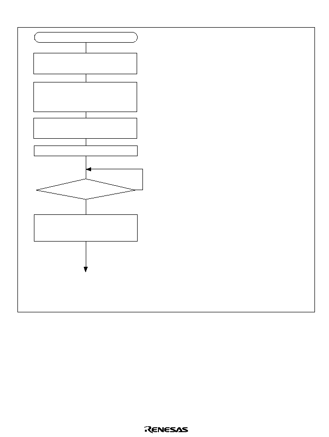
489
Figure 13.4 shows a sample flowchart for initializing the SCI.
Start of initialization
Set value in BRR
Select communication format
in SMR
1-bit interval elapsed?
Wait
(4)
(3)
(2)
(1)
Yes
No
<End of initialization>
Note: In simultaneous transmitting and receiving, the TE and RE bits should be cleared to
0 or set to 1 simultaneously.
Set TE or RE bit to 1 in SCR
Set the RIE, TIE, TEIE, and
MPIE bits
Set CKE1 and CKE0 bits in SCR
(leaving TE and RE bits
cleared to 0)
Clear TE and RE bits
to 0 in SCR
(1)
(2)
(3)
(4)
Set the clock source in SCR. Clear the
RIE, TIE, TEIE, MPIE, TE, and RE bits to
0. If clock output is selected in asynchro-
nous mode, clock output starts immedi-
ately after the setting is made in SCR.
Select the communication format in SMR.
Write the value corresponding to the bit
rate in BRR.
This step is not necessary when an
external clock is used.
Wait for at least the interval required to
transmit or receive one bit, then set the
TE or RE bit to 1 in SCR. Set the RIE,
TIE, TEIE, and MPIE bits as necessary.
Setting the TE or RE bit enables the SCI
to use the TxD or RxD pin.
Figure 13.4 Sample Flowchart for SCI Initialization
490
�
Transmitting Serial Data (Asynchronous Mode): Figure 13.5 shows a sample flowchart for
transmitting serial data and indicates the procedure to follow.
Yes
Yes
<End>
Clear TE bit to 0 in SCR
Clear DR bit to 0 and set
DDR bit to 1
TEND = 1
No
Output break signal?
No
Read TEND flag in SSR
All data transmitted?
No
TDRE = 1
Yes
No
Read TDRE flag in SSR
(3)
Initialize
(4)
Write transmit data in TDR
and clear TDRE flag to 0 in SSR
(1)
(2)
(3)
(4)
Start transmitting
(1)
(2)
Yes
SCI initialization:
the transmit data output function of the TxD pin is
selected automatically.
Transmission is possible after the TE bit is set to 1
and 1 is output for one frame.
SCI status check and transmit data write:
read SSR and check that the TDRE flag is set to 1,
then write transmit data in TDR and clear the TDRE
flag to 0.
To continue transmitting serial data:
after checking that the TDRE flag is 1, indicating that
data can be written, write data in TDR, then clear the
TDRE flag to 0. When the DMAC is activated by a
transmit-data-empty interrupt request (TXI) to write
data in TDR, the TDRE flag is checked and cleared
automatically.
To output a break signal at the end of serial
transmission:
set the DDR bit to 1 and clear the DR bit to 0, then
clear the TE bit to 0 in SCR.
Figure 13.5 Sample Flowchart for Transmitting Serial Data
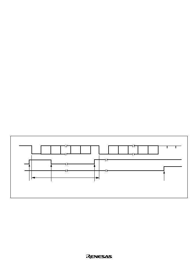
491
In transmitting serial data, the SCI operates as follows:
�
The SCI monitors the TDRE flag in SSR. When the TDRE flag is cleared to 0, the SCI
recognizes that TDR contains new data, and loads this data from TDR into TSR.
�
After loading the data from TDR to TSR, the SCI sets the TDRE flag to 1 and starts
transmitting. If the TIE bit is set to 1 in SCR, the SCI requests a transmit-data-empty interrupt
(TXI) at this time.
Serial transmit data is transmitted in the following order from the TxD pin:
Start bit: One 0 bit is output.
Transmit data: 7 or 8 bits are output, LSB first.
Parity bit or multiprocessor bit: One parity bit (even or odd parity),or one multiprocessor
bit is output. Formats in which neither a parity bit nor a multiprocessor bit is output can
also be selected.
Stop bit(s): One or two 1 bits (stop bits) are output.
Mark state: Output of 1 bits continues until the start bit of the next transmit data.
�
The SCI checks the TDRE flag when it outputs the stop bit. If the TDRE flag is 0, the SCI
loads new data from TDR into TSR, outputs the stop bit, then begins serial transmission of the
next frame. If the TDRE flag is 1, the SCI sets the TEND flag to 1 in SSR, outputs the stop
bit, then continues output of 1 bits in the mark state. If the TEIE bit is set to 1 in SCR, a
transmit-end interrupt (TEI) is requested at this time.
Figure 13.6 shows an example of SCI transmit operation in asynchronous mode.
0/1
D0
D1
D7
0/1
1
1
0
Start bit
0
D0
D1
D7
1
1
Data
Parity
bit
Stop
bit
Start
bit
Data
Parity
bit
Stop
bit
TDRE
TEND
Idle state
(mark state)
TEI interrupt
request
TXI interrupt
request
TXI interrupt handler
writes data in TDR and
clears TDRE flag to 0
TXI interrupt
request
1 frame
Figure 13.6 Example of SCI Transmit Operation in Asynchronous Mode
(8-Bit Data with Parity and One Stop Bit)
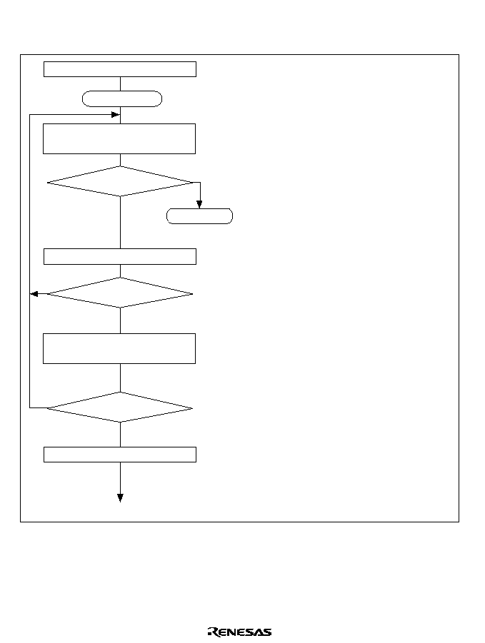
492
�
Receiving Serial Data (Asynchronous Mode): Figure 13.7 shows a sample flowchart for
receiving serial data and indicates the procedure to follow.
Yes
Yes
No
No
<End>
All data received?
(2)
(1)
Initialize
(4)
(5)
(1)
(2)(3)
(4)
(5)
Start receiving
Error handling
Read ORER, PER, and FER
flags in SSR
PER
FER
OPER = 1
RDRF = 1
Read RDRF flag in SSR
(continued on next page)
Read receive data from RDR, and
clear RDRF flag to 0 in SSR
Yes
(3)
No
SCI initialization:
the receive data input function of the RxD
pin is selected automatically.
Receive error handling and break detection:
if a receive error occurs, read the ORER,
PER, and FER flags in SSR to identify the
error. After executing the necessary error
handling, clear the ORER, PER, and FER
flags all to 0. Receiving cannot resume if
any of these flags remains set to 1. When a
framing error occurs, the RxD pin can be
read to detect the break state.
SCI status check and receive data read:
read SSR, check that the RDRF flag is set
to 1, then read receive data from RDR and
clear the RDRF flag to 0. Notification that
the RDRF flag has changed from 0 to 1 can
also be given by the RXI interrupt.
To continue receiving serial data:
check the RDRF flag, read RDR, and clear
the RDRF flag to 0 before the stop bit of the
current frame is received. When the DMAC
is activated by a receive-data-full interrupt
request (RXI) to read RDR, the RDRF flag
is cleared automatically.
Clear RE bit to 0 in SCR
Figure 13.7 Sample Flowchart for Receiving Serial Data (1)
493
Yes
<End>
Error handling
Yes
No
Yes
Yes
No
No
No
ORER = 1
Overrun error handling
FER = 1
Break?
Framing error handling
Clear RE bit to 0 in SCR
PER = 1
Parity error handling
Clear ORER, PER, and FER flags
to 0 in SSR
(3)
Figure 13.7 Sample Flowchart for Receiving Serial Data (2)

494
In receiving, the SCI operates as follows:
�
The SCI monitors the communication line. When it detects a start bit (0 bit), the SCI
synchronizes internally and starts receiving.
�
Receive data is stored in RSR in order from LSB to MSB.
�
The parity bit and stop bit are received.
After receiving these bits, the SCI carries out the following checks:
Parity check: The number of 1s in the receive data must match the even or odd parity
setting of in the O/
E bit in SMR.
Stop bit check: The stop bit value must be 1. If there are two stop bits, only the first is
checked.
Status check: The RDRF flag must be 0, indicating that the receive data can be transferred
from RSR into RDR.
If these all checks pass, the RDRF flag is set to 1 and the received data is stored in RDR. If
one of the checks fails (receive error*), the SCI operates as shown in table 13.11.
Note: *
When a receive error occurs, further receiving is disabled. In receiving, the RDRF flag
is not set to 1. Be sure to clear the error flags to 0.
�
When the RDRF flag is set to 1, if the RIE bit is set to 1 in SCR, a receive-data-full interrupt
(RXI) is requested. If the ORER, PER, or FER flag is set to 1 and the RIE bit in SCR is also
set to 1, a receive-error interrupt (ERI) is requested.
Table 13.11 Receive Error Conditions
Receive Error Abbreviation Condition
Data Transfer
Overrun error ORER
Receiving of next data ends while
RDRF flag is still set to 1 in SSR
Receive data is not transferred
from RSR to RDR
Framing error FER
Stop bit is 0
Receive data is transferred from
RSR to RDR
Parity error
PER
Parity of received data differs from
even/odd parity setting in SMR
Receive data is transferred from
RSR to RDR
495
Figure 13.8 shows an example of SCI receive operation in asynchronous mode.
0/1
D0
D1
D7
0/1
1
1
0
Start
bit
0
D0
D1
D7
1
1
Data
Data
Parity
bit
Parity
bit
Stop
bit
Stop
bit
Stop
bit
Start
bit
RDRF
FER
Idle (mark) state
Framing error,
ERI request
RXI request
RXI interrupt handler
reads data in RDR and
clears RDRF flag to 0
1 frame
Figure 13.8 Example of SCI Receive Operation
(8-Bit Data with Parity and One Stop Bit)
13.3.3
Multiprocessor Communication
The multiprocessor communication function enables several processors to share a single serial
communication line. The processors communicate in asynchronous mode using a format with an
additional multiprocessor bit (multiprocessor format).
In multiprocessor communication, each receiving processor is addressed by an ID. A serial
communication cycle consists of an ID-sending cycle that identifies the receiving processor, and a
data-sending cycle. The multiprocessor bit distinguishes ID-sending cycles from data-sending
cycles.
The transmitting processor stars by sending the ID of the receiving processor with which it wants
to communicate as data with the multiprocessor bit set to 1. Next the transmitting processor sends
transmit data with the multiprocessor bit cleared to 0.
Receiving processors skip incoming data until they receive data with the multiprocessor bit set to
1. When they receive data with the multiprocessor bit set to 1, receiving processors compare the
data with their IDs. Processors with IDs not matching the received data skip further incoming data
until they again receive data with the multiprocessor bit set to 1. Multiple processors can send and
receive data in this way.
Figure 13.9 shows an example of communication among different processors using a
multiprocessor format.
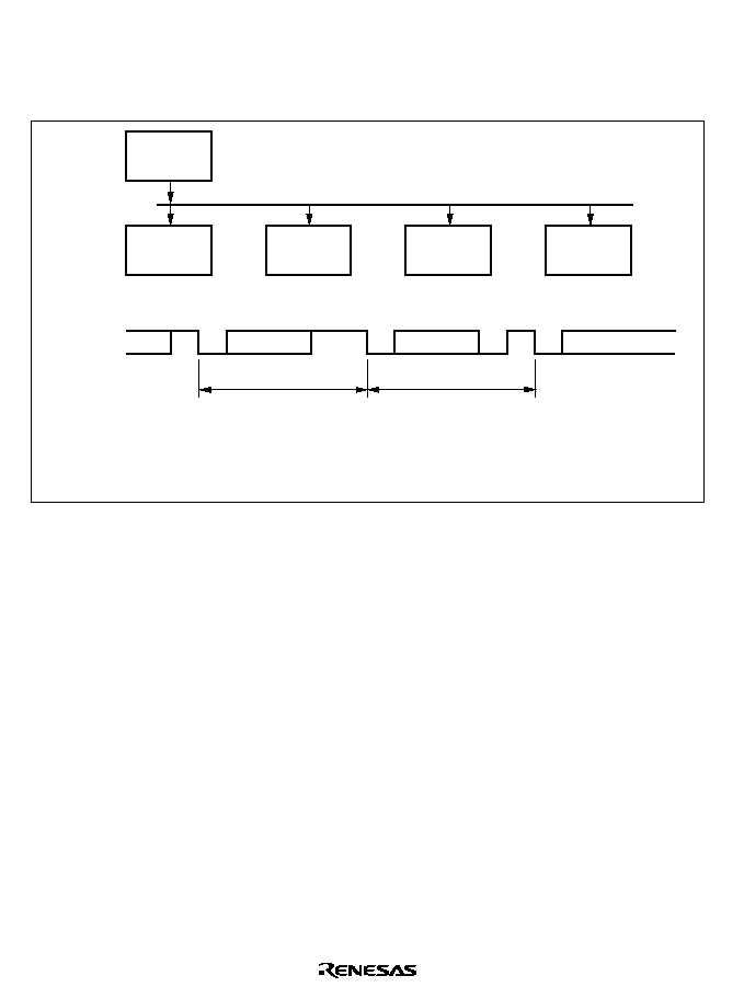
496
Communication Formats: Four formats are available. Parity bit settings are ignored when a
multiprocessor format is selected. For details see table 13.10.
Clock: See the description of asynchronous mode.
(ID=04)
(ID=01)
(ID=02)
(ID=03)
Transmitting
processor
Receiving
processor B
Receiving
processor A
Receiving
processor C
Receiving
processor D
H'01
(MPB=1)
Serial data
H'AA
(MPB=0)
Serial communication line
ID-sending cycle:
receiving processor address
Data-sending cycle:
data sent to receiving processor
specified by ID
Legend
MPB : Multiprocessor bit
Figure 13.9 Example of Communication among Processors using Multiprocessor Format
(Sending Data H'AA to Receiving Processor A)
Transmitting and Receiving Data:
�
Transmitting Multiprocessor Serial Data: Figure 13.10 shows a sample flowchart for
transmitting multiprocessor serial data and indicates the procedure to follow.
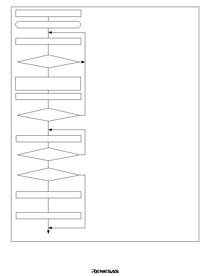
497
TEND = 1
No
No
Read TEND flag in SSR
Yes
Yes
Yes
Yes
No
No
<End>
Clear TE bit to 0 in SCR
Clear DR bit to 0 and set DDR to 1
(2)
(1)
Initialize
(3)
(4)
(1)
(2)
(3)
(4)
TDRE = 1
All data transmitted?
Read TDRE flag in SSR
Start transmitting
Write transmit data in TDR
and set MPBT bit in SSR
Clear TDRE flag to 0
Output break signal?
SCI initialization:
the transmit data output function of the TxD pin
is selected automatically.
SCI status check and transmit data write:
read SSR, check that the TDRE flag is 1, then
write transmit data in TDR. Also set the MPBT
flag to 0 or 1 in SSR. Finally, clear the TDRE
flag to 0.
To continue transmitting serial data:
after checking that the TDRE flag is 1,
indicating that data can be written, write data
in TDR, then clear the TDRE flag to 0. When
the DMAC is activated by a transmit-data-
empty interrupt request (TXI) to write data in
TDR, the TDRE flag is checked and cleared
automatically.
To output a break signal at the end of serial
transmission:
set the DDR bit to 1 and clear the DR bit to 0,
then clear the TE bit to 0 in SCR.
Figure 13.10 Sample Flowchart for Transmitting Multiprocessor Serial Data
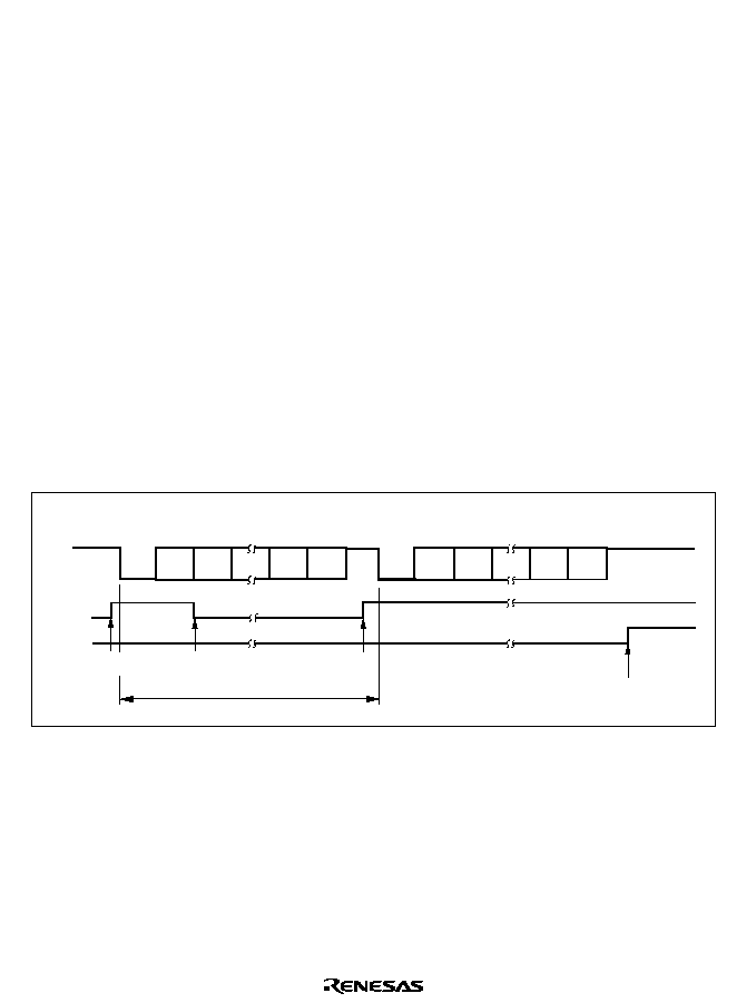
498
In transmitting serial data, the SCI operates as follows:
�
The SCI monitors the TDRE flag in SSR. When the TDRE flag is cleared to 0, the SCI
recognizes that TDR contains new data, and loads this data from TDR into TSR.
�
After loading the data from TDR to TSR, the SCI sets the TDRE flag to 1 and starts
transmitting. If the TIE bit is set to 1 in SCR, the SCI requests a transmit-data-empty interrupt
(TXI) at this time.
Serial transmit data is transmitted in the following order from the TxD pin:
Start bit: One 0 bit is output.
Transmit data: 7 or 8 bits are output, LSB first.
Multiprocessor bit: One multiprocessor bit (MPBT value) is output.
Stop bit(s): One or two 1 bits (stop bits) are output.
Mark state: Output of 1 bits continues until the start bit of the next transmit data.
�
The SCI checks the TDRE flag when it outputs the stop bit. If the TDRE flag is 0, the SCI
loads new data from TDR into TSR, outputs the stop bit, then begins serial transmission of the
next frame. If the TDRE flag is 1, the SCI sets the TEND flag to 1 in SSR, outputs the stop
bit, then continues output of 1 bits in the mark state. If the TEIE bit is set to 1 in SCR, a
transmit-end interrupt (TEI) is requested at this time.
Figure 13.11 shows an example of SCI transmit operation using a multiprocessor format.
D0
D1
D7
0/1
1
1
0
Start
bit
0
D0
D1
D7
0/1
1
Data
Multi-
processor
bit
Stop
bit
Start
bit
Data
Multi-
processor
bit
Stop
bit
TDRE
TEND
Idle (mark)
state
TEI interrupt
request
TXI interrupt
request
TXI interrupt handler
writes data in TDR and
clears TDRE flag to 0
TXI interrupt
request
1 frame
Figure 13.11 Example of SCI Transmit Operation
(8-Bit Data with Multiprocessor Bit and One Stop Bit)
�
Receiving Multiprocessor Serial Data: Figure 13.12 shows a sample flowchart for receiving
multiprocessor serial data and indicates the procedure to follow.
499
Read RDRF flag in SSR
No
Yes
Yes
Yes
No
Yes
Yes
No
No
No
Read ORER and FER flags
in SSR
(3)
(1)
(2)
(4)
(1)
(2)
(3)
(4)
(5)
RDRF = 1
FER
ORER = 1
FER
ORER = 1
Start receiving
Own ID?
<End>
RDRF = 1
Read RDRF flag in SSR
Finished receiving?
Read receive data from RDR
Yes
Clear RE bit to 0 in SCR
(5)
Error handling
(continued on next page)
SCI initialization:
the receive data input function of the
RxD pin is selected automatically.
ID receive cycle:
set the MPIE bit to 1 in SCR.
SCI status check and ID check:
read SSR, check that the RDRF flag
is set to 1, then read data from RDR
and compare it with the processor's
own ID. If the ID does not match, set
the MPIE bit to 1 again and clear the
RDRF flag to 0. If the ID matches,
clear the RDRF flag to 0.
SCI status check and data receiving:
read SSR, check that the RDRF flag
is set to 1, then read data from RDR.
Receive error handling and break
detection:
if a receive error occurs, read the
ORER and FER flags in SSR to
identify the error. After executing the
necessary error handling, clear the
ORER and FER flags both to 0.
Receiving cannot resume while either
the ORER or FER flag remains set to
1. When a framing error occurs, the
RxD pin can be read to detect the
break state.
No
Set MPIE bit to 1 in SCR
Read ORER and FER flags
in SSR
Read RDRF flag in SSR
Initialize
Figure 13.12 Sample Flowchart for Receiving Multiprocessor Serial Data (1)
500
Yes
Yes
No
No
<End>
Clear ORER, PER, and FER
flags to 0 in SSR
Clear RE bit to 0 in SCR
(5)
Error handling
ORER = 1
FER = 1
No
Break?
Overrun error handling
Framing error handling
Yes
Figure 13.12 Sample Flowchart for Receiving Multiprocessor Serial Data (2)
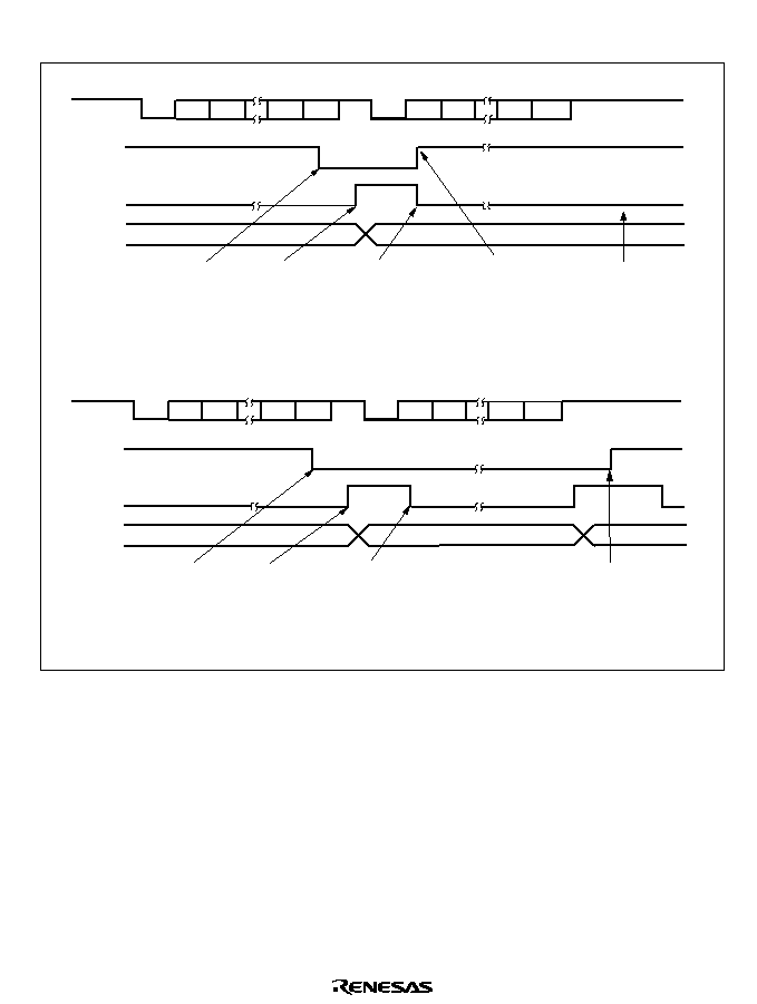
501
Figure 13.13 shows an example of SCI receive operation using a multiprocessor format.
ID2
Data2
Idle (mark)
state
Not own ID, so MPIE
bit is set to 1 again
a. Own ID does not match data
b. Own ID matches data
D0
D1
D7
1
1
0
Start
bit
Start
bit
Stop
bit
Stop
bit
0
D0
D1
D7
0
1
1
Data (ID1)
Data (data1)
Start
bit
Stop
bit
Stop
bit
Data (data1)
MPIE
Idle (mark)
state
1
MPB
RDRF
RDR value
RDR value
RXI interrupt
request
(multiprocessor
interrupt)
MPB detection
MPIE = 0
RXI interrupt handler reads
RDR data and clears
RDRF flag to 0
No RXI interrupt
request, RDR not
updated
ID1
MPB
D0
D1
D7
1
1
0
Start
bit
0
D0
D1
D7
0
1
1
Data (ID2)
MPIE
1
MPB
RDRF
RXI interrupt
request
(multiprocessor
interrupt)
RXI interrupt handler
reads RDR data and
clears RDRF flag to 0
Own ID, so receiving
continues, with data
received by RXI
interrupt handler
MPB
ID1
MPIE bit is set to
1 again
MPB detection
MPIE = 0
Figure 13.13 Example of SCI Receive Operation
(8-Bit Data with Multiprocessor Bit and One Stop Bit)
13.3.4
Synchronous Operation
In synchronous mode, the SCI transmits and receives data in synchronization with clock pulses.
This mode is suitable for high-speed serial communication.
The SCI transmitter and receiver share the same clock but are otherwise independent, so full-
duplex communication is possible. The transmitter and the receiver are also double-buffered, so
continuous transmitting or receiving is possible by reading or writing data while transmitting or
receiving is in progress.
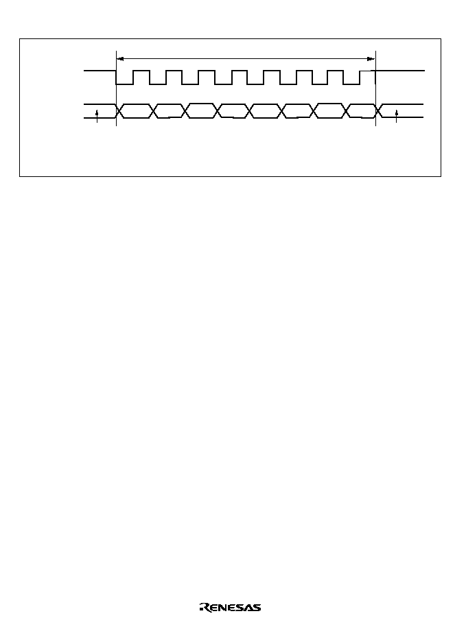
502
Figure 13.14 shows the general format in synchronous serial communication.
Don't care
One unit (character or frame) of transfer data
MSB
Bit 0
Bit 1
Bit 3
Bit 2
Bit 4
Bit 5
Bit 6
Bit 7
L S B
Don't care
Serial clock
Serial data
*
*
Note:
*
High except in continuous transmitting or receiving
Figure 13.14 Data Format in Synchronous Communication
In synchronous serial communication, each data bit is placed on the communication line from one
falling edge of the serial clock to the next. Data is guaranteed valid at the rise of the serial clock.
In each character, the serial data bits are transferred in order from LSB (first) to MSB (last). After
output of the MSB, the communication line remains in the state of the MSB. In synchronous
mode the SCI receives data by synchronizing with the rise of the serial clock.
Communication Format: The data length is fixed at 8 bits. No parity bit or multiprocessor bit
can be added.
Clock: An internal clock generated by the on-chip baud rate generator or an external clock input
from the SCK pin can be selected by means of the C/
A bit in SMR and the CKE1 and CKE0 bits
in SCR. See table 13.6 for details of SCI clock source selection.
When the SCI operates on an internal clock, it outputs the clock source at the SCK pin. Eight
clock pulses are output per transmitted or received character. When the SCI is not transmitting or
receiving, the clock signal remains in the high state. If receiving in single-character units is
required, an external clock should be selected.
Transmitting and Receiving Data:
�
SCI Initialization (Synchronous Mode): Before transmitting or receiving data, clear the TE and
RE bits to 0 in SCR, then initialize the SCI as follows.
When changing the communication mode or format, always clear the TE and RE bits to 0
before following the procedure given below. Clearing TE to 0 sets the TDRE flag to 1 and
initializes TSR. Note that clearing RE to 0, however, does not initialize the RDRF, PER, and
ORE flags, or RDR, which retain their previous contents.
503
Figure 13.15 shows a sample flowchart for initializing the SCI.
<Start transmitting or receiving>
(4)
(3)
(2)
(1)
Start of initialization
Yes
Wait
No
1-bit interval elapsed?
Set value in BRR
Clear TE and RE bits to 0 in SCR
Select communication format
in SMR
Set RIE, TIE, TEIE, MPIE, CKE1,
and CKE0 bits in SCR (leaving
TE and RE bits cleared to 0)
Set TE or RE bit to 1 in SCR
Set RIE, TIE, TEIE, and MPIE
bits as necessary
(1)
(2)
(3)
(4)
Note:
*
Set the clock source in SCR. Clear the RIE,
TIE, TEIE, MPIE, TE, and RE bits to 0.
*
Select the communication format in SMR.
Write the value corresponding to the bit rate in
BRR.
This step is not necessary when an external
clock is used.
Wait for at least the interval required to transmit
or receive one bit, then set the TE or RE bit to
1 in SCR.
*
Set the RIE, TIE, TEIE, and MPIE
bits as necessary. Setting the TE or RE bit
enables the SCI to use the TxD or RxD pin.
In simultaneous transmitting and receiving,
the TE and RE bits should be cleared to 0 or
set to 1 simultaneously.
Figure 13.15 Sample Flowchart for SCI Initialization
504
�
Transmitting Serial Data (Synchronous Mode): Figure 13.16 shows a sample flowchart for
transmitting serial data and indicates the procedure to follow.
<End>
Yes
Yes
Clear TE bit to 0 in SCR
Yes
No
No
(2)
(1)
Initialize
(3)
(1)
(2)
(3)
Start transmitting
TDRE = 1
All data transmitted?
Read TEND flag in SSR
Read TDRE flag in SSR
Write transmit data in TDR
and clear TDRE flag to 0 in SSR
TEND = 1
No
SCI initialization: the transmit data output
function of the TxD pin is selected
automatically.
SCI status check and transmit data write:
read SSR, check that the TDRE flag is 1, then
write transmit data in TDR and clear the
TDRE flag to 0.
To continue transmitting serial data: after
checking that the TDRE flag is 1, indicating
that data can be written, write data in TDR,
then clear the TDRE flag to 0. When the
DMAC is activated by a transmit-data-empty
interrupt request (TXI) to write data in TDR,
the TDRE flag is checked and cleared
automatically.
Figure 13.16 Sample Flowchart for Serial Transmitting
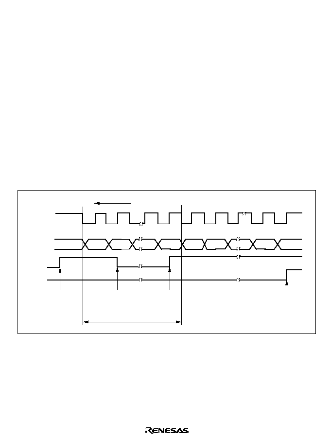
505
In transmitting serial data, the SCI operates as follows.
�
The SCI monitors the TDRE flag in SSR. When the TDRE flag is cleared to 0, the SCI
recognizes that TDR contains new data, and loads this data from TDR into TSR.
�
After loading the data from TDR to TSR, the SCI sets the TDRE flag to 1 and starts
transmitting. If the TIE bit is set to 1 in SCR, the SCI requests a transmit-data-empty interrupt
(TXI) at this time.
If clock output is selected, the SCI outputs eight serial clock pulses. If an external clock source
is selected, the SCI outputs data in synchronization with the input clock. Data is output from
the TxD pin n order from LSB (bit 0) to MSB (bit 7).
�
The SCI checks the TDRE flag when it outputs the MSB (bit 7). If the TDRE flag is 0, the SCI
loads data from TDR into TSR and begins serial transmission of the next frame. If the TDRE
flag is 1, the SCI sets the TEND flag to 1 in SSR, and after transmitting the MSB (bit 7), holds
the TxD pin in the MSB state. If the TEIE bit is set to 1 in SCR, a transmit-end interrupt (TEI)
is requested at this time
�
After the end of serial transmission, the SCK pin is held in a constant state.
Figure 13.17 shows an example of SCI transmit operation.
Bit 0
Bit 1
Bit 7
Bit 0
Bit 1
Bit 6
Bit 7
Serial clock
Serial data
1 frame
TXI interrupt
request
TXI interrupt handler
writes data in TDR
and clears TDRE
flag to 0
TXI interrupt
request
TEI interrupt
request
Transmit direction
TEND
TDRE
Figure 13.17 Example of SCI Transmit Operation
�
Receiving Serial Data (Synchronous Mode): Figure 13.18 shows a sample flowchart for
receiving serial data and indicates the procedure to follow. When switching from
asynchronous to synchronous mode. make sure that the ORER, PER, and FER flags are cleared
to 0. If the FER or PER flag is set to 1 the RDRF flag will not be set and both transmitting and
receiving will be disabled.
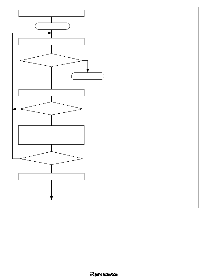
506
Yes
Yes
No
No
<End>
Clear RE bit to 0 in SCR
Finished receiving?
(2)
(1)
Initialize
(4)
(3)
(5)
(1)
(2)(3)
(4)
(5)
Start receiving
Error handling
ORER = 1
RDRF = 1
Read RDRF flag in SSR
Read ORER flag in SSR
(continued on next page)
Read receive data from
RDR, and clear RDRF
flag to 0 in SSR
No
Yes
SCI initialization: the receive data
input function of the RxD pin is
selected automatically.
Receive error handling: if a receive
error occurs, read the ORER flag in
SSR, then after executing the
necessary error handling, clear the
ORER flag to 0. Neither transmitting
nor receiving can resume while the
ORER flag remains set to 1.
SCI status check and receive data
read: read SSR, check that the RDRF
flag is set to 1, then read receive data
from RDR and clear the RDRF flag to
0. Notification that the RDRF flag
has changed from 0 to 1 can also be
given by the RXI interrupt.
To continue receiving serial data:
check the RDRF flag, read RDR, and
clear the RDRF flag to 0 before the
MSB (bit 7) of the current frame is
received. When the DMAC is
activated by a receive-data-full
interrupt request (RXI) to read RDR,
the RDRF flag is cleared
automatically.
Figure 13.18 Sample Flowchart for Serial Receiving (1)
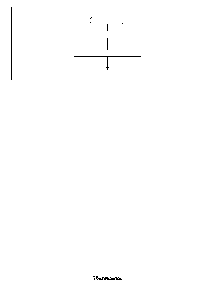
507
<End>
(3)
Error handling
Overrun error handling
Clear ORER flag to 0 in SSR
Figure 13.18 Sample Flowchart for Serial Receiving (2)
In receiving, the SCI operates as follows:
�
The SCI synchronizes with serial clock input or output and synchronizes internally.
�
Receive data is stored in RSR in order from LSB to MSB.
After receiving the data, the SCI checks that the RDRF flag is 0, so that receive data can be
transferred from RSR to RDR. If this check passes, the RDRF flag is set to 1 and the received
data is stored in RDR. If the checks fails (receive error), the SCI operates as shown in table
13.11.
When a receive error has been identified in the error check, subsequent transmit and receive
operations are disabled.
�
When the RDRF flag is set to 1, if the RIE bit is set to 1 in SCR, a receive-data-full interrupt
(RXI) is requested. If the ORER flag is set to 1 and the RIE bit in SCR is also set to 1, a
receive-error interrupt (ERI) is requested.
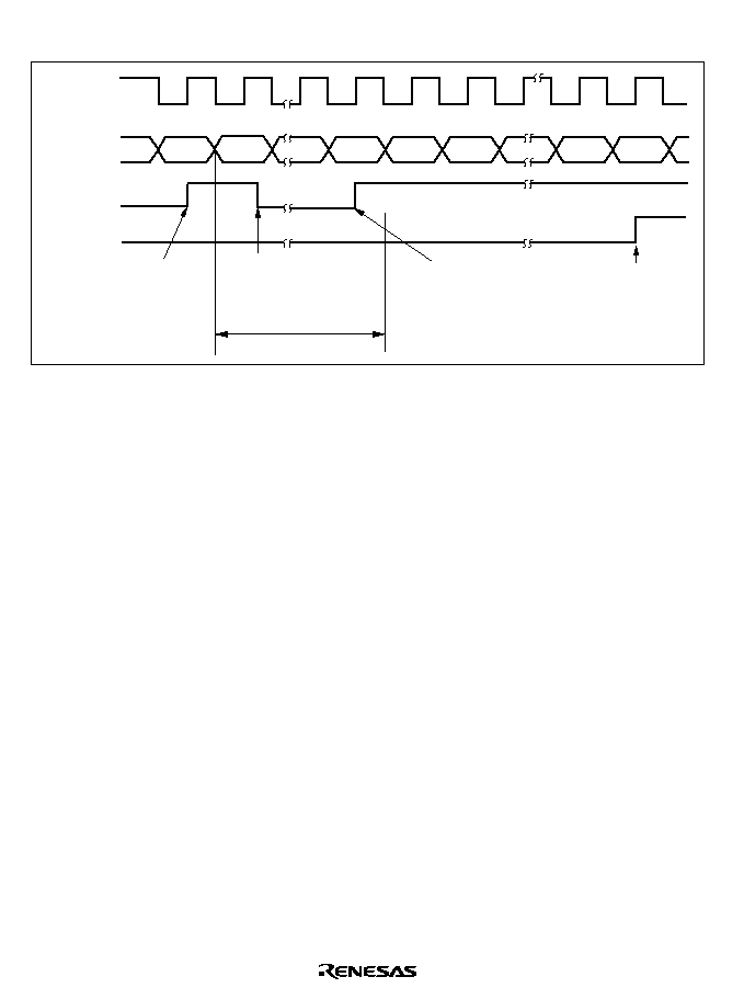
508
Figure 13.19 shows an example of SCI receive operation.
Serial clock
Serial data
RXI interrupt handler
reads data in RDR and
clears RDRF flag to 0
RXI interrupt
request
RXI interrupt
request
Overrun error,
ERI interrupt
request
ORER
RDRF
Bit 7
Bit 0
Bit 7
Bit 0
Bit 1
Bit 6
Bit 7
1 frame
Figure 13.19 Example of SCI Receive Operation
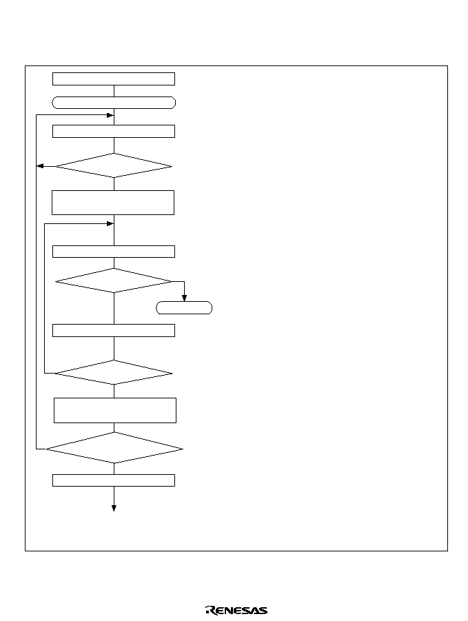
509
�
Transmitting and Receiving Data Simultaneously (Synchronous Mode): Figure 13.20 shows a
sample flowchart for transmitting and receiving serial data simultaneously and indicates the
procedure to follow.
Yes
No
No
<End>
Read receive data from RDR, and
clear RDRF flag to 0 in SSR
Yes
No
No
(2)
(1)
Initialize
(3)
(5)
(4)
(1)
(2)
(3)
(4)
(5)
Start of transmitting and receiving
Error handling
TDRE = 1
ORER = 1
Read ORER flag in SSR
Read RDRF flag in SSR
Read TDRE flag in SSR
Write transmit data in TDR and
clear TDRE flag to 0 in SSR
Yes
End of transmitting
and receiving?
Clear TE and RE bits to 0 in SCR
RDRF = 1
Yes
SCI initialization: the transmit data output function of the
TxD pin and the read data input function of the RxD pin
are selected, enabling simultaneous transmitting and
receiving.
SCI status check and transmit data write: read SSR, check
that the TDRE flag is 1, then write transmit data in TDR
and clear the TDRE flag to 0.
Notification that the TDRE flag has changed from 0 to 1
can also be given by the TXI interrupt.
Receive error handling: if a receive error occurs, read the
ORER flag in SSR, then after executing the necessary
error handling, clear the ORER flag to 0.
Neither transmitting nor receiving can resume while the
ORER flag remains set to 1.
SCI status check and receive data read: read SSR, check
that the RDRF flag is 1, then read receive data from RDR
and clear the RDRF flag to 0. Notification that the RDRF
flag has changed from 0 to 1 can also be given by the RXI
interrupt.
To continue transmitting and receiving serial data: check
the RDRF flag, read RDR, and clear the RDRF flag to 0
before the MSB (bit 7) of the current frame is received.
Also check that the TDRE flag is set to 1, indicating that
data can be written, write data in TDR, then clear the
TDRE flag to 0 before the MSB (bit 7) of the current frame
is transmitted. When the DMAC is activated by a transmit-
data-empty interrupt request (TXI) to write data in TDR,
the TDRE flag is checked and cleared automatically.
When the DMAC is activated by a receive-data-full
interrupt request (RXI) to read RDR, the RDRF flag is
cleared automatically.
Note: When switching from transmitting or receiving to simultaneous transmitting and receiving, clear both the TE bit
and the RE bit to 0, then set both bits to 1 simultaneously.
Figure 13.20 Sample Flowchart for Simultaneous Serial Transmitting and Receiving

510
13.4
SCI Interrupts
The SCI has four interrupt request sources: the transmit-end interrupt (TEI), receive-error interrupt
(ERI), receive-data-full interrupt (RXI), and transmit-data-empty interrupt (TXI). Table 13.12 lists
the interrupt sources and indicates their priority. These interrupts can be enabled or disabled by the
TIE, RIE, and TEIE bits in SCR. Each interrupt request is sent separately to the interrupt
controller.
A TXI interrupt is requested when the TDRE flag is set to 1 in SSR. A TEI interrupt is requested
when the TEND flag is set to 1 in SSR. A TXI interrupt request can activate the DMAC to transfer
data. Data transfer by the DMAC automatically clears the TDRE flag to 0. A TEI interrupt request
cannot activate the DMAC.
An RXI interrupt is requested when the RDRF flag is set to 1 in SSR. An ERI interrupt is
requested when the ORER, PER, or FER flag is set to 1 in SSR. An RXI interrupt can activate the
DMAC to transfer data. Data transfer by the DMAC automatically clears the RDRF flag to 0. An
ERI interrupt request cannot activate the DMAC.
The DMAC can be activated by interrupts from SCI channel 0.
Table 13.12 SCI Interrupt Sources
Interrupt Source
Description
Priority
ERI
Receive error (ORER, FER, or PER)
High
RXI
Receive data register full (RDRF)
TXI
Transmit data register empty (TDRE)
TEI
Transmit end (TEND)
Low
13.5
Usage Notes
13.5.1
Notes on Use of SCI
Note the following points when using the SCI.
TDR Write and TDRE Flag: The TDRE flag in SSR is a status flag indicating the loading of
transmit data from TDR to TSR. The SCI sets the TDRE flag to 1 when it transfers data from
TDR to TSR.
Data can be written into TDR regardless of the state of the TDRE flag. If new data is written in
TDR when the TDRE flag is 0, the old data stored in TDR will be lost because this data has not
yet been transferred to TSR. Before writing transmit data in TDR, be sure to check that the TDRE
flag is set to 1.

511
Simultaneous Multiple Receive Errors: Table 13.13 shows the state of the SSR status flags
when multiple receive errors occur simultaneously. When an overrun error occurs the RSR
contents are not transferred to RDR, so receive data is lost.
Table 13.13 SSR Status Flags and Transfer of Receive Data
SSR Status Flags
Receive Data
Transfer
RDRF
ORER
FER
PER
RSR
RDR
Receive Errors
1
1
0
0
�
Overrun error
0
0
1
0
Framing error
0
0
0
1
Parity error
1
1
1
0
�
Overrun error +
framing error
1
1
0
1
�
Overrun error +
parity error
0
0
1
1
Framing error +
parity error
1
1
1
1
�
Overrun error +
framing error +
parity error
Notes:
: Receive data is transferred from RSR to RDR.
�
: Receive data is not transferred from RSR to RDR.
Break Detection and Processing: Break signals can be detected by reading the RxD pin directly
when a framing error (FER) is detected. In the break state the input from the RxD pin consists of
all 0s, so the FER flag is set and the parity error flag (PER) may also be set. In the break state the
SCI receiver continues to operate, so if the FER flag is cleared to 0 it will be set to 1 again.
Sending a Break Signal: The input/output condition and level of the TxD pin are determined by
DR and DDR bits. This feature can be used to send a break signal.
After the serial transmitter is initialized, the DR value substitutes for the mark state until the TE bit
is set to 1 (the TxD pin function is not selected until the TE bit is set to 1). The DDR and DR bits
should therefore be set to 1 beforehand.
To send a break signal during serial transmission, clear the DR bit to 0 , then clear the TE bit to 0.
When the TE bit is cleared to 0 the transmitter is initialized, regardless of its current state, so the
TxD pin becomes an input/output outputting the value 0.
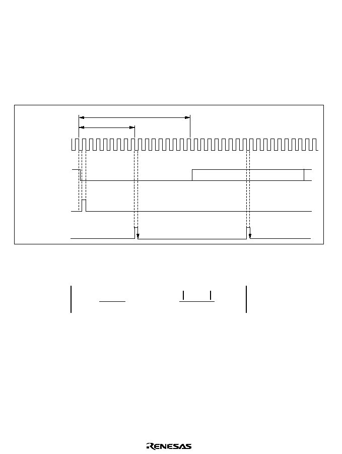
512
Receive Error Flags and Transmitter Operation (Synchronous Mode Only): When a receive
error flag (ORER, PER, or FER) is set to 1 the SCI will not start transmitting, even if the TDRE
flag is cleared to 0. Be sure to clear the receive error flags to 0 when starting to transmit. Note
that clearing the RE bit to 0 does not clear the receive error flags to 0.
Receive Data Sampling Timing in Asynchronous Mode and Receive Margin: In asynchronous
mode the SCI operates on a base clock with 16 times the bit rate frequency. In receiving, the SCI
synchronizes internally with the fall of the start bit, which it samples on the base clock. Receive
data is latched at the rising edge of the eighth base clock pulse. See figure 13.21.
15 0
Internal base clock
8 clocks
7
0
Receive data
(RxD)
Synchronization
sampling timing
Data sampling
timing
15 0
D
0
D
1
Start bit
16 clocks
7
Figure 13.21 Receive Data Sampling Timing in Asynchronous Mode
The receive margin in asynchronous mode can therefore be expressed as shown in equation (1).
M =
(0.5 �
1
2N
D � 0.5
N
) � (L � 0.5) F �
(1 + F)
�
100%
. . . . . . . . (1)
M:
Receive margin (%)
N:
Ratio of clock frequency to bit rate (N = 16)
D:
Clock duty cycle (L = 0 to 1.0)
L:
Frame length (L = 9 to 12)
F:
Absolute deviation of clock frequency
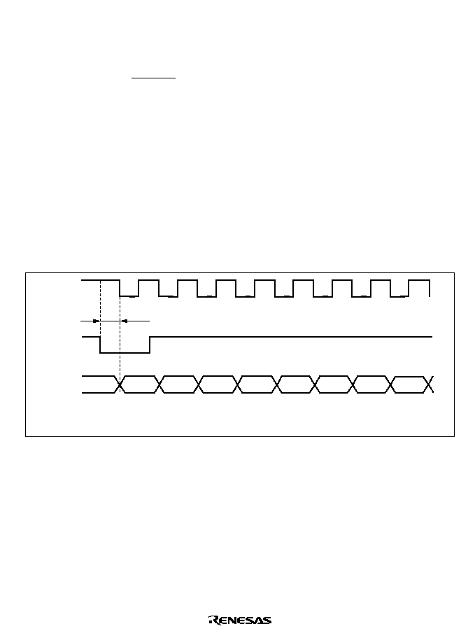
513
From equation (1), if F = 0 and D = 0.5, the receive margin is 46.875%, as given by equation (2).
M =
2
�
16
)
�
100%
(0.5
�
1
D = 0.5, F = 0
= 46.875%
. . . . . . . . (2)
This is a theoretical value. A reasonable margin to allow in system designs is 20% to 30%.
Restrictions on Use of DMAC:
�
When an external clock source is used for the serial clock, after the DMAC updates TDR,
allow an inversion of at least five system clock (
) cycles before input of the serial clock to
start transmitting. If the serial clock is input within four states of the TDR update, a
malfunction may occur (see figure 13.22) .
�
To have the DMAC read RDR, be sure to select the corresponding SCI receive-data-full
interrupt (RXI) as the activation source with bits DTS2 to DTS0 in DTCR.
SCK
D0
D1
D2
D3
D4
D5
D6
D7
TDRE
t
Note: In operation with an external clock source, be sure that t >4 states.
Figure 13.22 Example of Synchronous Transmission Using DMAC
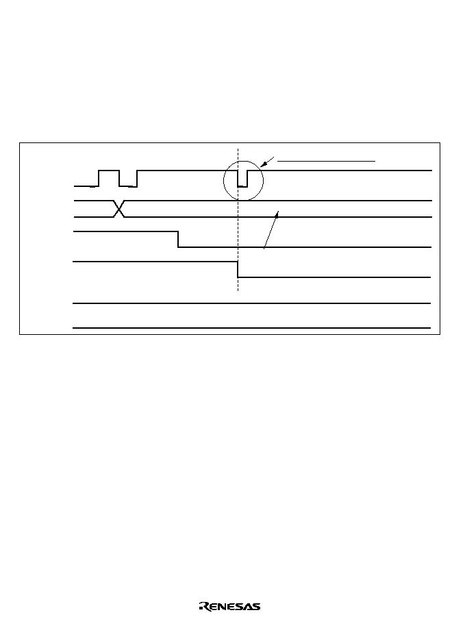
514
Switching from SCK Pin Function to Port Pin Function:
�
Problem in Operation: When switching the SCK pin function to the output port function (high-
level output) by making the following settings while DDR = 1, DR = 1, C/
A = 1, CKE1 = 0,
CKE0 = 0, and TE = 1 (synchronous mode), low-level output occurs for one half-cycle.
1. End of serial data transmission
2. TE bit = 0
3. C/
A bit = 0 ... switchover to port output
4. Occurrence of low-level output (see figure 13.23)
SCK/port
Data
TE
C/
A
CKE1
CKE0
Bit 7
Bit 6
1. End of transmission
4. Low-level output
3. C/
A
= 0
2. TE= 0
Half-cycle low-level output
Figure 13.23 Operation when Switching from SCK Pin Function to Port Pin Function
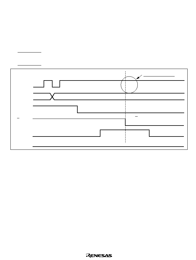
515
�
Sample Procedure for Avoiding Low-Level Output: As this sample procedure temporarily
places the SCK pin in the input state, the SCK/port pin should be pulled up beforehand with an
external circuit.
With DDR = 1, DR = 1, C/
A = 1, CKE1 = 0, CKE0 = 0, and TE = 1, make the following
settings in the order shown.
1. End of serial data transmission
2. TE bit = 0
3.
CKE1 bit = 1
4. C/
A bit = 0 ... switchover to port output
5.
CKE1 bit = 0
SCK/port
Data
TE
C/A
CKE1
CKE0
Bit 7
Bit 6
1. End of transmission
3. CKE1= 1
5. CKE1= 0
4. C/A= 0
2. TE= 0
High-level outputTE
Figure 13.24 Operation when Switching from SCK Pin Function to Port Pin Function
(Example of Preventing Low-Level Output)

516

517
Section 14 Smart Card Interface
14.1
Overview
An IC card (smart card) interface conforming to the ISO/IEC 7816-3 (Identification Card)
standard is supported as an extension of the serial communication interface (SCI) functions.
Switchover between the normal serial communication interface and the smart card interface is
controlled by a register setting.
14.1.1
Features
Features of the smart card interface supported by the H8/3069F are listed below.
�
Asynchronous communication
Data length: 8 bits
Parity bit generation and checking
Transmission of error signal (parity error) in receive mode
Error signal detection and automatic data retransmission in transmit mode
Direct convention and inverse convention both supported
�
Built-in baud rate generator allows any bit rate to be selected
�
Three interrupt sources
There are three interrupt sources--transmit-data-empty, receive-data-full, and
transmit/receive error--that can issue requests independently.
The transmit-data-empty interrupt and receive-data-full interrupt can activate the DMA
controller (DMAC) to execute data transfer.
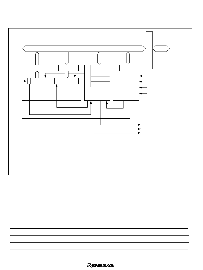
518
14.1.2
Block Diagram
Figure 14.1 shows a block diagram of the smart card interface.
Bus interface
TDR
RSR
RDR
Module data bus
TSR
SCMR
SSR
SCR
Transmission/
reception
control
BRR
Baud rate
generator
Internal
data bus
RxD
TxD
SCK
Parity generation
Parity check
Clock
External clock
/4
/16
/64
TXI
RXI
ERI
SMR
Legend
SCMR: Smart card mode register
RSR:
Receive shift register
RDR:
Receive data register
TSR:
Transmit shift register
TDR:
Transmit data register
SMR:
Serial mode register
SCR:
Serial control register
SSR:
Serial status register
BRR:
Bit rate register
Figure 14.1 Block Diagram of Smart Card Interface
14.1.3
Pin Configuration
Table 14.1 shows the smart card interface pins.
Table 14.1
Smart Card Interface Pins
Pin Name
Abbreviation
I/O
Function
Serial clock pin
SCK
I/O
Clock input/output
Receive data pin
RxD
Input
Receive data input
Transmit data pin
TxD
Output
Transmit data output

519
14.1.4
Register Configuration
The smart card interface has the internal registers listed in table 14.2. The BRR, TDR, and RDR
registers have their normal serial communication interface functions, as described in section 13,
Serial Communication Interface.
Table 14.2
Smart Card Interface Registers
Channel
Address
*
1
Name
Abbreviation
R/W
Initial Value
0
H'FFFB0
Serial mode register
SMR
R/W
H'00
H'FFFB1
Bit rate register
BRR
R/W
H'FF
H'FFFB2
Serial control register
SCR
R/W
H'00
H'FFFB3
Transmit data register
TDR
R/W
H'FF
H'FFFB4
Serial status register
SSR
R/(W)
*
2
H'84
H'FFFB5
Receive data register
RDR
R
H'00
H'FFFB6
Smart card mode register
SCMR
R/W
H'F2
1
H'FFFB8
Serial mode register
SMR
R/W
H'00
H'FFFB9
Bit rate register
BRR
R/W
H'FF
H'FFFBA
Serial control register
SCR
R/W
H'00
H'FFFBB
Transmit data register
TDR
R/W
H'FF
H'FFFBC
Serial status register
SSR
R/(W)
*
2
H'84
H'FFFBD
Receive data register
RDR
R
H'00
H'FFFBE
Smart card mode register
SCMR
R/W
H'F2
2
H'FFFC0
Serial mode register
SMR
R/W
H'00
H'FFFC1
Bit rate register
BRR
R/W
H'FF
H'FFFC2
Serial control register
SCR
R/W
H'00
H'FFFC3
Transmit data register
TDR
R/W
H'FF
H'FFFC4
Serial status register
SSR
R/(W)
*
2
H'84
H'FFFC5
Receive data register
RDR
R
H'00
H'FFFC6
Smart card mode register
SCMR
R/W
H'F2
Notes:
*
1 Lower 20 bits of the address in advanced mode.
*
2 Only 0 can be written in bits 7 to 3, to clear the flags.
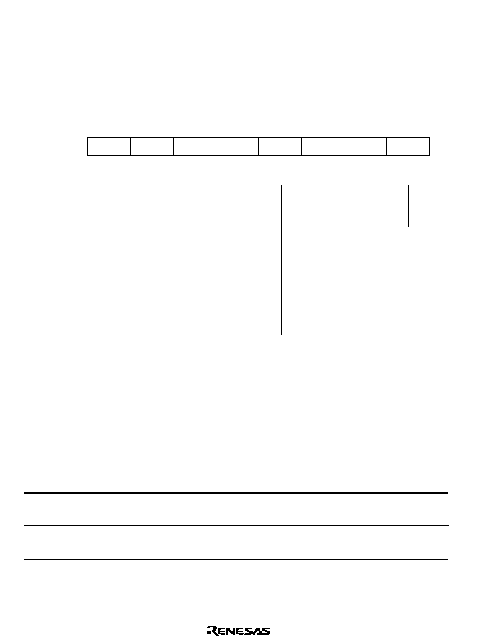
520
14.2
Register Descriptions
This section describes the new or modified registers and bit functions in the smart card interface.
14.2.1
Smart Card Mode Register (SCMR)
SCMR is an 8-bit readable/writable register that selects smart card interface functions.
7
--
1
--
6
--
1
--
5
--
1
--
4
--
1
--
3
SDIR
0
R/W
0
SMIF
0
R/W
2
SINV
0
R/W
1
--
1
--
Bit
Initial value
Read/Write
Reserved bits
Reserved bit
Smart card interface
mode select
Enables or disables
the smart card interface
function
Smart card data invert
Inverts data logic levels
Smart card data transfer direction
Selects the serial/parallel conversion format
SCMR is initialized to H'F2 by a reset and in standby mode.
Bits 7 to 4--Reserved: Read-only bits, always read as 1.
Bit 3--Smart Card Data Transfer Direction (SDIR): Selects the serial/parallel conversion
format.*
1
Bit 3
SDIR
Description
0
TDR contents are transmitted LSB-first
(Initial value)
Receive data is stored LSB-first in RDR
1
TDR contents are transmitted MSB-first
Receive data is stored MSB-first in RDR

521
Bit 2--Smart Card Data Invert (SINV): Specifies inversion of the data logic level. This
function is used in combination with the SDIR bit to communicate with inverse-convention
cards.*
2
The SINV bit does not affect the logic level of the parity bit. For parity settings, see
section 14.3.4, Register Settings.
Bit 2
SINV
Description
0
Unmodified TDR contents are transmitted
(Initial value)
Receive data is stored unmodified in RDR
1
Inverted TDR contents are transmitted
Receive data is inverted before storage in RDR
Bit 1--Reserved: Read-only bit, always read as 1.
Bit 0--Smart Card Interface Mode Select (SMIF): Enables the smart card interface function.
Bit 0
SMIF
Description
0
Smart card interface function is disabled
(Initial value)
1
Smart card interface function is enabled
Notes: *1 The function for switching between LSB-first and MSB-first mode can also be used
with the normal serial communication interface. Note that when the communication
format data length is set to 7 bits and MSB-first mode is selected for the serial data to
be transferred, bit 0 of TDR is not transmitted, and only bits 7 to 1 of the received data
are valid.
*2 The data logic level inversion function can also be used with the normal serial
communication interface. Note that, when inverting the serial data to be transferred,
parity transmission and parity checking is based on the number of high-level periods at
the serial data I/O pin, and not on the register value.
14.2.2
Serial Status Register (SSR)
The function of SSR bit 4 is modified in smart card interface mode. This change also causes a
modification to the setting conditions for bit 2 (TEND).

522
7
TDRE
1
R/(W)
*
6
RDRF
0
R/(W)
*
5
ORER
0
R/(W)
*
4
ERS
0
R/(W)
*
3
PER
0
R/(W)
*
0
MPBT
0
R/W
2
TEND
1
R
1
MPB
0
R
Bit
Initial value
Read/Write
Transmit end
Status flag indicating end
of transmission
Error signal status (ERS)
Status flag indicating that an error
signal has been received
Note:
*
Only 0 can be written, to clear the flag.
Bits 7 to 5: These bits operate as in normal serial communication. For details see section 13.2.7,
Serial Status Register (SSR).
Bit 4--Error Signal Status (ERS): In smart card interface mode, this flag indicates the status of
the error signal sent from the receiving device to the transmitting device. The smart card interface
does not detection framing errors.
Bit 4
ERS
Description
0
Indicates normal transmission, with no error signal returned
(Initial value)
[Clearing conditions]
The chip is reset, or enters standby mode or module stop mode
Software reads ERS while it is set to 1, then writes 0.
1
Indicates that the receiving device sent an error signal reporting a parity error
[Setting condition]
A low error signal was sampled.
Note:
Clearing the TE bit to 0 in SCR does not affect the ERS flag, which retains its previous
value.
Bits 3 to 0: These bits operate as in normal serial communication. For details see section 13.2.7,
Serial Status Register (SSR). The setting conditions for transmit end (TEND), however, are
modified as follows.

523
Bit 2
TEND
Description
0
Transmission is in progress
[Clearing conditions]
Software reads TDRE while it is set to 1, then writes 0 in the TDRE flag.
The DMAC or DTC writes data in TDR.
1
End of transmission
[Setting conditions]
(Initial value)
The chip is reset or enters standby mode.
The TE bit and FER/ERS bit are both cleared to 0 in SCR.
TDRE is 1 and ERS is 0 at a time 2.5 etu after the last bit of a 1-byte serial character
is transmitted (normal transmission).
Note:
An etu (elementary time unit) is the time needed to transmit one bit.
14.2.3
Serial Mode Register (SMR)
The function of SMR bit 7 is modified in smart card interface mode. This change also causes a
modification to the function of bits 1 and 0 in the serial control register (SCR).
7
GM
0
R/W
6
CHR
0
R/W
5
PE
0
R/W
4
O/E
0
R/W
3
STOP
0
R/W
0
CKS0
0
R/W
2
MP
0
R/W
1
CKS1
0
R/W
Bit
Initial value
Read/Write
Bit 7--GSM Mode (GM): With the normal smart card interface, this bit is cleared to 0. Setting
this bit to 1 selects GSM mode, an additional mode for controlling the timing for setting the
TEND flag that indicates completion of transmission, and the type of clock output used. The
details of the additional clock output control mode are specified by the CKE1 and CKE0 bits in
the serial control register (SCR).
Bit 7
GM
Description
0
Normal smart card interface mode operation
The TEND flag is set 12.5 etu after the beginning of the start bit.
Clock output on/off control only.
(Initial value)
1
GSM mode smart card interface mode operation
The TEND flag is set 11.0 etu after the beginning of the start bit.
Clock output on/off and fixed-high/fixed-low control.

524
Bit 6: Only 0 should be written to this bit.
Bits 5 to 2: These bits operate as in normal serial communication. For details see section 13.2.5,
Serial Mode Register (SMR).
Bits 1 and 0: Only 0 should be written to these bits.
14.2.4
Serial Control Register (SCR)
The function of SCR bits 1 and 0 is modified in smart card interface mode
7
TIE
0
R/W
6
RIE
0
R/W
5
TE
0
R/W
4
RE
0
R/W
3
MPIE
0
R/W
0
CKE0
0
R/W
2
TEIE
0
R/W
1
CKE1
0
R/W
Bit
Initial value
Read/Write
Bits 7 to 2: These bits operate as in normal serial communication. For details see section 13.2.6,
Serial Control Register (SCR).
Bits 1 and 0--Clock Enable 1 and 0 (CKE1, CKE0): These bits select the SCI clock source and
enable or disable clock output from the SCK pin. In smart card interface mode, it is possible to
specify a fixed high level or fixed low level for the clock output, in addition to the usual switching
between enabling and disabling of the clock output.
Bit 7
GM
Bit 1
CKE1
Bit 0
CKE0
Description
0
0
0
Internal clock/SCK pin is I/O port
(Initial value)
1
Internal clock/SCK pin is clock output
1
0
Internal clock/SCK pin is fixed at low output
1
Internal clock/SCK pin is clock output
1
0
Internal clock/SCK pin is fixed at high output
1
Internal clock/SCK pin is clock output
14.3
Operation
14.3.1
Overview
The main features of the smart card interface are as follows.
�
One frame consists of 8-bit data plus a parity bit.
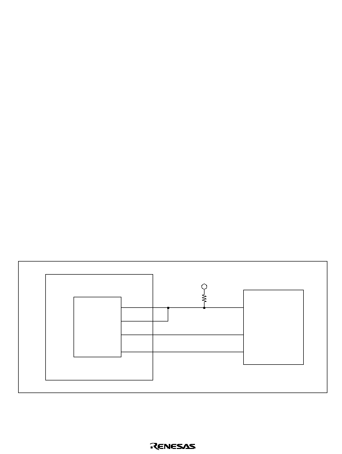
525
�
In transmission, a guard time of at least 2 etu (elementary time units: the time for transfer of
one bit) is provided between the end of the parity bit and the start of the next frame.
�
If a parity error is detected during reception, a low error signal level is output for a1 etu period
10.5 etu after the start bit.
�
If an error signal is detected during transmission, the same data is transmitted automatically
after the elapse of 2 etu or longer.
�
Only asynchronous communication is supported; there is no synchronous communication
function.
14.3.2
Pin Connections
Figure 14.2 shows a pin connection diagram for the smart card interface.
In communication with a smart card, since both transmission and reception are carried out on a
single data transmission line, the TxD pin and RxD pin should both be connected to this line. The
data transmission line should be pulled up to V
CC
with a resistor.
When the smart card uses the clock generated on the smart card interface, the SCK pin output is
input to the CLK pin of the smart card. If the smart card uses an internal clock, this connection is
unnecessary.
The reset signal should be output from one of the H8/3069F's generic ports.
In addition to these pin connections, power and ground connections will normally also be
necessary.
TxD
RxD
SCK
Px (port)
H8/3069F
chip
V
CC
I/O
Data line
Clock line
Reset line
CLK
RST
Card-processing device
Smart card
Figure 14.2 Smart Card Interface Connection Diagram
Note:
A loop-back test can be performed by setting both RE and TE to 1 without connecting a
smart card.
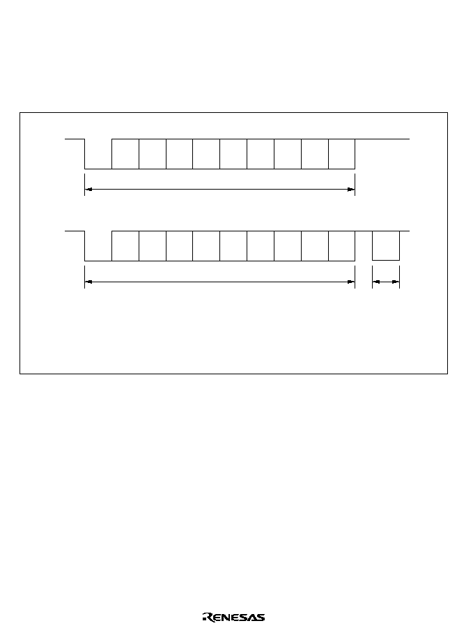
526
14.3.3
Data Format
Figure 14.3 shows the smart card interface data format. In reception in this mode, a parity check is
carried out on each frame, and if an error is detected an error signal is sent back to the transmitting
device to request retransmission of the data. In transmission, the error signal is sampled and the
same data is retransmitted if the error signal is low.
Ds
D0
D1
D2
D3
D4
D5
D6
D7
Dp
No parity error
Output from transmitting device
Ds
D0
D1
D2
D3
D4
D5
D6
D7
Dp
Parity error
Output from transmitting device
DE
Output from
receiving
device
Legend
Ds: Start
bit
D0 to D7: Data bits
Dp: Parity
bit
DE: Error
signal
Figure 14.3 Smart Card Interface Data Format
The operating sequence is as follows.
1. When the data line is not in use it is in the high-impedance state, and is fixed high with a pull-
up resistor.
2. The transmitting device starts transfer of one frame of data. The data frame starts with a start
bit (Ds, low-level), followed by 8 data bits (D0 to D7) and a parity bit (Dp).
3. With the smart card interface, the data line then returns to the high-impedance state. The data
line is pulled high with a pull-up resistor.
4. The receiving device carries out a parity check. If there is no parity error and the data is
received normally, the receiving device waits for reception of the next data. If a parity error
occurs, however, the receiving device outputs an error signal (DE, low-level) to request
retransmission of the data. After outputting the error signal for the prescribed length of time,
the receiving device places the signal line in the high-impedance state again. The signal line is
pulled high again by a pull-up resistor.

527
5. If the transmitting device does not receive an error signal, it proceeds to transmit the next data
frame. If it receives an error signal, however, it returns to step 2 and transmits the same data
again.
14.3.4
Register Settings
Table 14.3 shows a bit map of the registers used in the smart card interface. Bits indicated as 0 or
1 must be set to the value shown. The setting of other bits is described in this section.
Table 14.3
Smart Card Interface Register Settings
Bit
Register
Address
*
1
Bit 7
Bit 6
Bit 5
Bit 4
Bit 3
Bit 2
Bit 1
Bit 0
SMR
H'FFFB0
GM
0
1
O/
E
1
0
CKS1
CKS0
BRR
H'FFFB1
BRR7
BRR6
BRR5
BRR4
BRR3
BRR2
BRR1
BRR0
SCR
H'FFFB2
TIE
RIE
TE
RE
0
0
CKE1
*
2
CKE0
TDR
H'FFFB3
TDR7
TDR6
TDR5
TDR4
TDR3
TDR2
TDR1
TDR0
SSR
H'FFFB4
TDRE
RDRF
ORER
ERS
PER
TEND
0
0
RDR
H'FFFB5
RDR7
RDR6
RDR5
RDR4
RDR3
RDR2
RDR1
RDR0
SCMR
H'FFFB6
--
--
--
--
SDIR
SINV
--
SMIF
Notes: -- Unused bit.
*
1 Lower 20 bits of the address in advanced mode.
*
2 When GM is cleared to 0 in SMR, the CKE1 bit must also be cleared to 0.
Serial Mode Register (SMR) Settings: Clear the GM bit to 0 when using the normal smart card
interface mode, or set to 1 when using GSM mode. Clear the O/
E bit to 0 if the smart card is of the
direct convention type, or set to 1 if of the inverse convention type.
Bits CKS1 and CKS0 select the clock source of the built-in baud rate generator. See section
14.3.5, Clock.
Bit Rate Register (BRR) Settings: BRR is used to set the bit rate. See section 14.3.5, Clock, for
the method of calculating the value to be set.
Serial Control Register (SCR) Settings: The TIE, RIE, TE, and RE bits have their normal serial
communication functions. See section 13, Serial Communication Interface, for details. The CKE1
and CKE0 bits specify clock output. To disable clock output, clear these bits to 00; to enable clock
output, set these bits to 01. Clock output is not performed when the GM bit is set to 1 in SMR.
Clock output can also be fixed low or high.

528
Smart Card Mode Register (SCMR) Settings: Clear both the SDIR bit and SINV bit cleared to
0 if the smart card is of the direct convention type, and set both to 1 if of the inverse convention
type. To use the smart card interface, set the SMIF bit to 1.
The register settings and examples of starting character waveforms are shown below for two smart
cards, one following the direct convention and one the inverse convention.
1. Direct Convention (SDIR = SINV = O/
E = 0)
Ds
D0
D1
D2
D3
D4
D5
D6
D7
Dp
A
Z
Z
A
Z
Z
Z
A
A
Z
(Z)
(Z)
State
With the direct convention type, the logic 1 level corresponds to state Z and the logic 0 level to
state A, and transfer is performed in LSB-first order. In the example above, the first character
data is H'3B. The parity bit is 1, following the even parity rule designated for smart cards.
2. Indirect Convention (SDIR = SINV = O/
E = 1)
Ds
D7
D6
D5
D4
D3
D2
D1
D0
Dp
A
Z
Z
A
A
A
A
A
A
Z
(Z)
(Z)
State
With the indirect convention type, the logic 1 level corresponds to state A and the logic 0 level
to state Z, and transfer is performed in MSB-first order. In the example above, the first
character data is H'3F. The parity bit is 0, corresponding to state Z, following the even parity
rule designated for smart cards.
In the H8/3069F, inversion specified by the SINV bit applies only to the data bits, D7 to D0.
For parity bit inversion, the O/
E bit in SMR must be set to odd parity mode. This applies to
both transmission and reception.

529
14.3.5
Clock
Only an internal clock generated by the on-chip baud rate generator can be used as the
transmit/receive clock for the smart card interface. The bit rate is set with the bit rate register
(BRR) and the CKS1 and CKS0 bits in the serial mode register (SMR). The equation for
calculating the bit rate is shown below. Table 14.5 shows some sample bit rates.
If clock output is selected with CKE0 set to 1, a clock with a frequency of 372 times the bit rate is
output from the SCK pin.
B =
1488
�
2
2n�1
�
(N + 1)
�
10
6
where, N: BRR setting (0
N
255)
B: Bit rate (bit/s)
: Operating frequency (MHz)
n: See table 14.4
Table 14.4
n-Values of CKS1 and CKS0 Settings
n
CKS1
CKS0
0
0
0
1
1
2
1
0
3
1
Note:
If the gear function is used to divide the clock frequency, use the divided frequency to
calculate the bit rate. The equation above applies directly to 1/1 frequency division.
Table 14.5
Bit Rates (bits/s) for Various BRR Settings (When n = 0)
(MHz)
N
7.1424
10.00
10.7136 13.00
14.2848 16.00
18.00
20.00
25.00
0
9600.0
13440.9 14400.0 17473.1 19200.0 21505.4 24193.5 26881.7 33602.2
1
4800.0
6720.4
7200.0
8736.6
9600.0
10752.7 12096.8 13440.9 16801.1
2
3200.0
4480.3
4800.0
5824.4
6400.0
7168.5
8064.5
8960.6
11200.7
Note:
Bit rates are rounded off to one decimal place.

530
The following equation calculates the bit rate register (BRR) setting from the operating frequency
and bit rate. N is an integer from 0 to 255, specifying the value with the smaller error.
N =
1488
�
2
2n�1
�
B
�
10
6
� 1
Table 14.6
BRR Settings for Typical Bit Rates (bits/s) (When n = 0)
(MHz)
7.1424
10.00
10.7136
13.00
14.2848
16.00
18.00
20.00
25.0
bit/s
N Error N Error N Error N Error N Error N Error N Error N Error N Error
9600
0 0.00
1 30
1 25
1 8.99
1 0.00
1 12.01 2 15.99 2 6.66
3 12.49
Table 14.7
Maximum Bit Rates for Various Frequencies (Smart Card Interface Mode)
(MHz)
Maximum Bit Rate (bits/s)
N
n
7.1424
9600
0
0
10.00
13441
0
0
10.7136
14400
0
0
13.00
17473
0
0
14.2848
19200
0
0
16.00
21505
0
0
18.00
24194
0
0
20.00
26882
0
0
25.00
33602
0
0
The bit rate error is given by the following equation:
Error (%) =
1488
�
2
2n-1
�
B
�
(N + 1)
�
10
6
� 1
�
100

531
14.3.6
Transmitting and Receiving Data
Initialization: Before transmitting or receiving data, the smart card interface must be initialized as
described below. Initialization is also necessary when switching from transmit mode to receive
mode, or vice versa.
1. Clear the TE and RE bits to 0 in the serial control register (SCR).
2. Clear error flags ERS, PER, and ORER to 0 in the serial status register (SSR).
3. Set the parity bit (O/
E) and baud rate generator select bits (CKS1 and CKS0) in the serial mode
register (SMR). Clear the C/
A, CHR, and MP bits to 0, and set the STOP and PE bits to 1.
4. Set the SMIF, SDIR, and SINV bits in the smart card mode register (SCMR).
When the SMIF bit is set to 1, the TxD pin and RxD pin are both switched from port to SCI
pin functions and go to the high-impedance state.
5. Set a value corresponding to the desired bit rate in the bit rate register (BRR).
6. Set the CKE0 bit in SCR. Clear the TIE, RIE, TE, RE, MPIE, TEIE, and CKE1 bits to 0. If the
CKE0 bit is set to 1, the clock is output from the SCK pin.
7. Wait at least one bit interval, then set the TIE, RIE, TE, and RE bits in SCR. Do not set the TE
bit and RE bit at the same time, except for self-diagnosis.
Transmitting Serial Data: As data transmission in smart card mode involves error signal
sampling and retransmission processing, the processing procedure is different from that for the
normal SCI. Figure 14.5 shows a sample transmission processing flowchart.
1. Perform smart card interface mode initialization as described in Initialization above.
2. Check that the ERS error flag is cleared to 0 in SSR.
3. Repeat steps 2 and 3 until it can be confirmed that the TEND flag is set to 1 in SSR.
4. Write the transmit data in TDR, clear the TDRE flag to 0, and perform the transmit operation.
The TEND flag is cleared to 0.
5. To continue transmitting data, go back to step 2.
6. To end transmission, clear the TE bit to 0.
The above processing may include interrupt handling DMA transfer.
If transmission ends and the TEND flag is set to 1 while the TIE bit is set to 1 and interrupt
requests are enabled, a transmit-data-empty interrupt (TXI) will be requested. If an error occurs in
transmission and the ERS flag is set to 1 while the RIE bit is set to 1 and interrupt requests are
enabled, a transmit/receive-error interrupt (ERI) will be requested.
The timing of TEND flag setting depends on the GM bit in SMR (see figure 14.4).
If the TXI interrupt activates the DMAC, the number of bytes designated in the DMAC can be
transmitted automatically, including automatic retransmission.
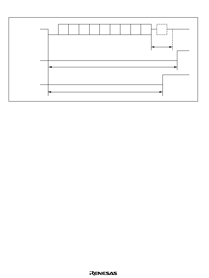
532
For details, see Interrupt Operations and Data Transfer by DMAC in this section.
Serial data
(1) GM = 0
TEND
(2) GM = 1
TEND
Ds
Dp
DE
Guard time
11.0 etu
12.5 etu
Figure 14.4 Timing of TEND Flag Setting
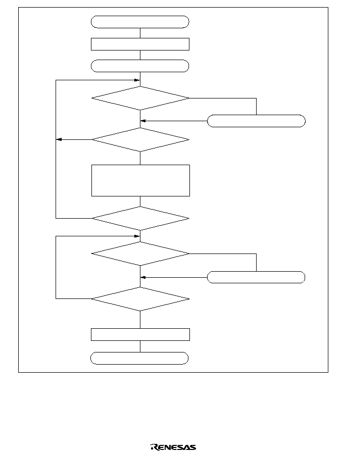
533
Initialization
No
Yes
Clear TE bit to 0
Start transmitting
Start
No
No
No
Yes
Yes
Yes
Yes
No
End
Write transmit data in TDR,
and clear TDRE flag
to 0 in SSR
Error handling
Error handling
TEND = 1?
All data transmitted?
TEND = 1?
ERS = 0?
ERS = 0?
Figure 14.5 Sample Transmission Processing Flowchart
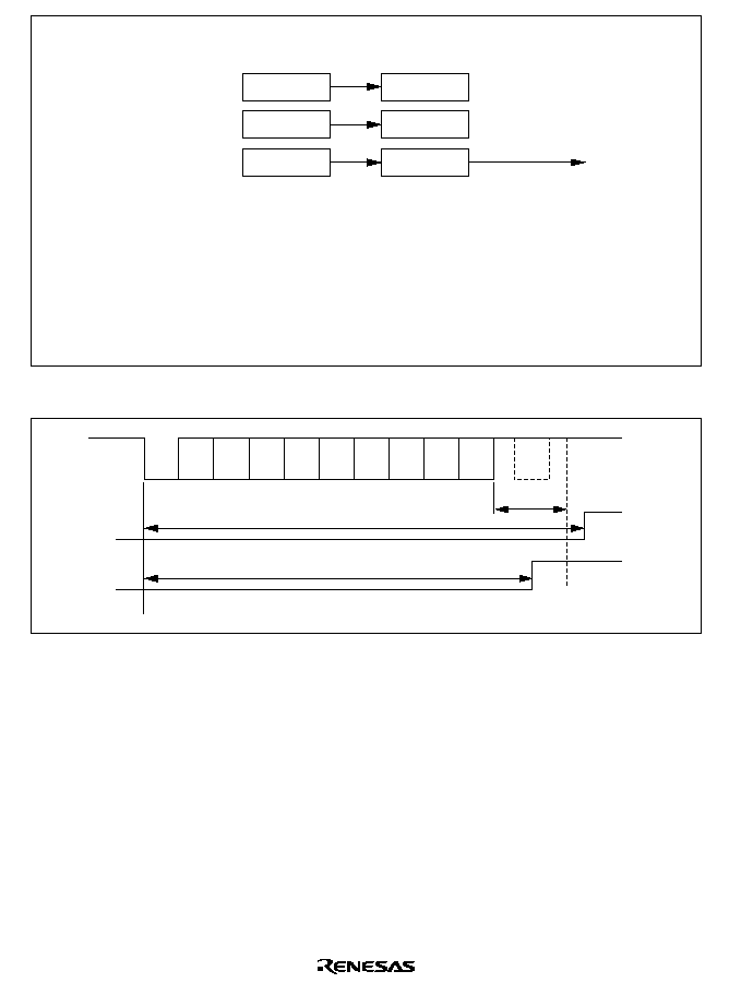
534
1. Data write
TDR
TSR
(shift register)
Data 1
2. Transfer from TDR to TSR
Data 1
Data 1
Data remains in TDR
Data 1
3. Serial data output
Note: When the ERS flag is set, it should be cleared until transfer of the last bit (D7 in LSB-first
transmission, D0 in MSB-first transmission) of the retransmit data to be transmitted next has
been completed.
In case of normal transmission: TEND flag is set
In case of transmit error:
ERS flag is set
Steps 2 and 3 above are repeated until the
TEND flag is set.
I/O signal
output
Data 1
Figure 14.6 Relation Between Transmit Operation and Internal Registers
I/O data
When GM = 0
Guard time
DE
Ds
Da
Db
Dc
Dd
De
Df
Dg
Dh
Dp
12.5 etu
11.0 etu
When GM = 1
TXI (TEND
interrupt)
Figure 14.7 Timing of TEND Flag Setting
Receiving Serial Data: Data reception in smart card mode uses the same processing procedure as
for the normal SCI. Figure 14.8 shows a sample reception processing flowchart.
1. Perform smart card interface mode initialization as described in Initialization above.
2. Check that the ORER flag and PER flag are cleared to 0 in SSR. If either is set, perform the
appropriate receive error handling, then clear both the ORER and the PER flag to 0.
3. Repeat steps 2 and 3 until it can be confirmed that the RDRF flag is set to 1.
4. Read the receive data from RDR.
5. To continue receiving data, clear the RDRF flag to 0 and go back to step 2.
6. To end reception, clear the RE bit to 0.
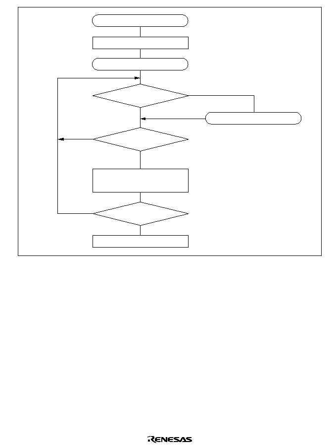
535
Initialization
Read RDR and clear
RDRF flag to 0 in SSR
Clear RE bit to 0
Start receiving
Start
Error handling
No
No
No
Yes
Yes
ORER = 0
and PER = 0?
RDRF = 1?
All data received?
Yes
Figure 14.8 Sample Reception Processing Flowchart
The above procedure may include interrupt handling and DMA transfer.
If reception ends and the RDRF flag is set to 1 while the RIE bit is set to 1 and interrupt requests
are enabled, a receive-data-full interrupt (RXI) will be requested. If an error occurs in reception
and either the ORER flag or the PER flag is set to 1, a transmit/receive-error interrupt (ERI) will
be requested.
If the RXI interrupt activates the DMAC, the number of bytes designated in the DMAC will be
transferred, skipping receive data in which an error occurred.
For details, see Interrupt Operations and Data Transfer by DMAC in this section.
If a parity error occurs during reception and the PER flag is set to 1, the received data is
transferred to RDR, so the erroneous data can be read.
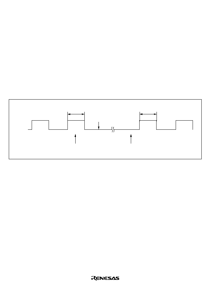
536
Switching Modes: When switching from receive mode to transmit mode, first confirm that the
receive operation has been completed, then start from initialization, clearing RE to 0 and setting
TE to 1. The RDRF, PER, or ORER flag can be used to check that the receive operation has been
completed.
When switching from transmit mode to receive mode, first confirm that the transmit operation has
been completed, then start from initialization, clearing TE to 0 and setting RE to 1. The TEND
flag can be used to check that the transmit operation has been completed.
Fixing Clock Output: When the GM bit is set to 1 in SMR, clock output can be fixed by means
of the CKE1 and CKE0 bits in SCR. The minimum clock pulse width can be set to the specified
width in this case.
Figure 14.9 shows the timing for fixing clock output. In this example, GM = 1, CKE1 = 0, and the
CKE0 bit is controlled.
Specified pulse
width
CKE1 value
SCK
Specified pulse
width
SCR write
(CKE0 = 1)
SCR write
(CKE0 = 0)
Figure 14.9 Timing for Fixing Cock Output
Interrupt Operations: The smart card interface has three interrupt sources: transmit-data-empty
(TXI), transmit/receive-error (ERI), and receive-data-full (RXI). The transmit-end interrupt
request (TEI) is not available in smart card mode.
A TXI interrupt is requested when the TEND flag is set to 1 in SSR. An RXI interrupt is requested
when the RDRF flag is set to 1 in SSR. An ERI interrupt is requested when the ORER, PER, or
ERS flag is set to 1 in SSR. These relationships are shown in table 14.8.

537
Table 14.8
Smart Card Interface Mode Operating States and Interrupt Sources
Operating State
Flag
Enable Bit
Interrupt
Source
DMAC
Activation
Transmit Mode
Normal
operation
TEND
TIE
TXI
Available
Error
ERS
RIE
ERI
Not available
Receive Mode
Normal
operation
RDRF
RIE
RXI
Available
Error
PER, ORER
RIE
ERI
Not available
Data Transfer by DMAC: The DMAC can be used to transmit and receive data in smart card
mode, as in normal SCI operations. In transmit mode, when the TEND flag is set to 1 in SSR, the
TDRE flag is set simultaneously, generating a TXI interrupt. If the TXI request is designated
beforehand as a DMAC activation source, the DMAC will be activated by the TXI request and
will transfer the next transmit data. This data transfer by the DMAC automatically clears the
TDRE and TEND flags to 0. In the event of an error, the SCI automatically retransmits the same
data, keeping the TEND flag cleared to 0 so that the DMAC is not activated. The SCI and DMAC
will therefore automatically transmit the designated number of bytes, including retransmission
when an error occurs. When an error occurs, the ERS flag is not cleared automatically, so the RIE
bit should be set to 1 to enable the error to generate an ERI request, and the ERI interrupt handler
should clear ERS.
When using the DMAC to transmit or receive, first set up and enable the DMAC, then make SCI
settings. DMAC settings are described in section 7, DMA controller.
In receive operations, an RXI interrupt is requested when the RDRF flag is set to 1 in SSR. If the
RXI request is designated beforehand as a DMAC activation source, the DMAC will be activated
by the RXI request and will transfer the received data. This data transfer by the DMAC
automatically clears the RDRF flag to 0. When an error occurs, the RDRF flag is not set and an
error flag is set instead. The DMAC is not activated. The ERI interrupt request is directed to the
CPU. The ERI interrupt handler should clear the error flags.
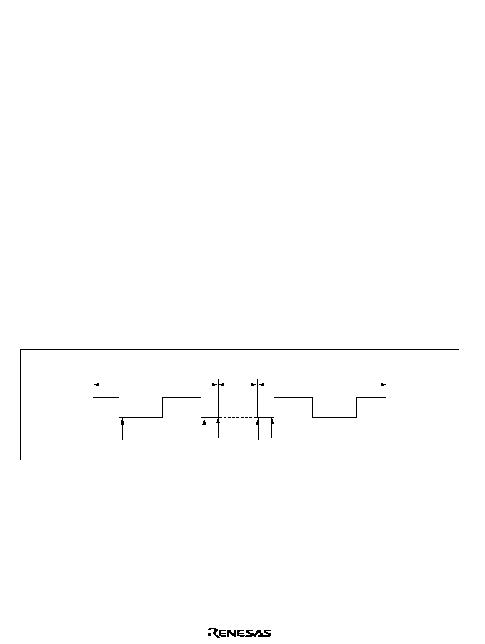
538
Examples of Operation in GSM Mode: When switching between smart card interface mode and
software standby mode, use the following procedures to maintain the clock duty cycle.
�
Switching from smart card interface mode to software standby mode
1. Set the P9
4
data register (DR) and data direction register (DDR) to the values for the fixed
output state in software standby mode.
2. Write 0 in the TE and RE bits in the serial control register (SCR) to stop transmit/receive
operations. At the same time, set the CKE1 bit to the value for the fixed output state in
software standby mode.
3. Write 0 in the CKE0 bit in SCR to stop the clock.
4. Wait for one serial clock cycle. During this period, the duty cycle is preserved and clock output
is fixed at the specified level.
5. Write H'00 in the serial mode register (SMR) and smart card mode register (SCMR).
6. Make the transition to the software standby state.
�
Returning from software standby mode to smart card interface mode
1. Clear the software standby state.
2. Set the CKE1 bit in SCR to the value for the fixed output state at the start of software standby
(the current P9
4
pin state).
3. Set smart card interface mode and output the clock. Clock signal generation is started with the
normal duty cycle.
Software
standby
Normal operation
Normal operation
(1) (2) (3)
(4) (5) (6)
(1) (2) (3)
Figure 14.10 Procedure for Stopping and Restarting the Clock
Use the following procedure to secure the clock duty cycle after powering on.
1. The initial state is port input and high impedance. Use pull-up or pull-down resistors to fix the
potential.
2. Fix at the output specified by the CKE1 bit in SCR.
3. Set SMR and SCMR, and switch to smart card interface mode operation.
4. Set the CKE0 bit to 1 in SCR to start clock output.
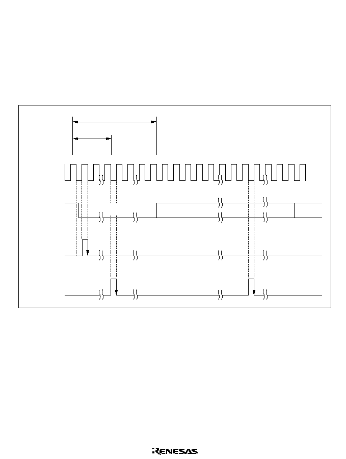
539
14.4
Usage Notes
The following points should be noted when using the SCI as a smart card interface.
Receive Data Sampling Timing and Receive Margin in Smart Card Interface Mode: In smart
card interface mode, the SCI operates on a base clock with a frequency of 372 times the transfer
rate. In reception, the SCI synchronizes internally with the fall of the start bit, which it samples on
the base clock. Receive data is latched at the rising edge of the 186th base clock pulse. The timing
is shown in figure 14.11.
Internal base
clock
372 clocks
186 clocks
Receive data
(RxD)
Synchronization
sampling timing
D0
D1
Data sampling
timing
185
371 0
371
185
0
0
Start bit
Figure 14.11 Receive Data Sampling Timing in Smart Card Interface Mode

540
The receive margin can therefore be expressed as follows.
Receive margin in smart card interface mode:
M = (0.5 �
1
2N
D � 0.5
N
) � (L � 0.5) F �
(1 + F)
�
100%
M: Receive margin (%)
N: Ratio of clock frequency to bit rate (N = 372)
D: Clock duty cycle (L = 0 to 1.0)
L: Frame length (L =10)
F: Absolute deviation of clock frequency
From the above equation, if F = 0 and D = 0.5, the receive margin is as follows.
When D = 0.5 and F = 0:
M = (0.5 � 1/2
�
372)
�
100%
= 49.866%
Retransmission: Retransmission is performed by the SCI in receive mode and transmit mode as
described below.
�
Retransmission when SCI is in Receive Mode
Figure 14.12 illustrates retransmission when the SCI is in receive mode.
1. If an error is found when the received parity bit is checked, the PER bit is automatically set to
1. If the RIE bit in SCR is set to the enable state, an ERI interrupt is requested. The PER bit
should be cleared to 0 in SSR before the next parity bit sampling timing.
2. The RDRF bit in SSR is not set for the frame in which the error has occurred.
3. If no error is found when the received parity bit is checked, the PER bit is not set to 1 in SSR.
4. If no error is found when the received parity bit is checked, the receive operation is assumed to
have been completed normally, and the RDRF bit is automatically set to 1 in SSR. If the RIE
bit in SCR is set to the enable state, an RXI interrupt is requested. If RXI is enabled as a DMA
transfer activation source, the RDR contents can be read automatically. When the DMAC reads
the RDR data, the RDRF flag is automatically cleared to 0.
5. When a normal frame is received, the data pin is held in the high-impedance state at the error
signal transmission timing.
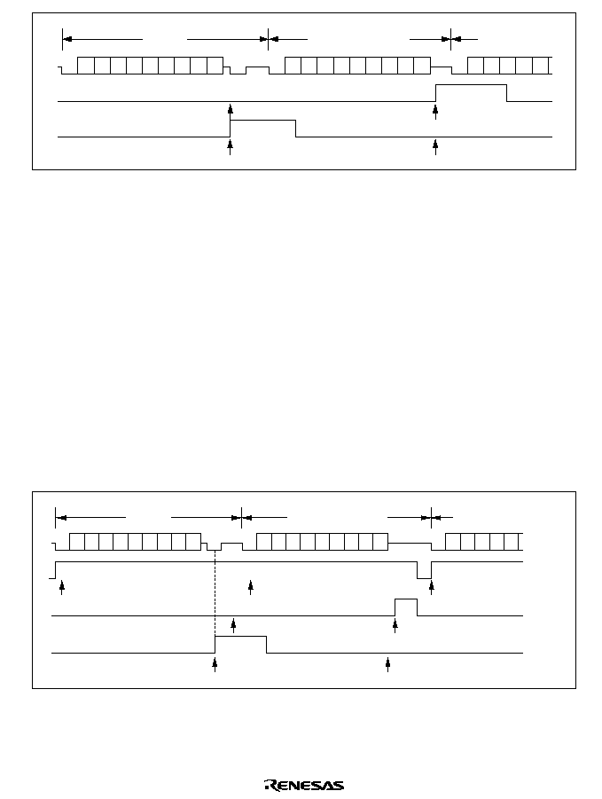
541
D0 D1 D2 D3 D4 D5 D6 D7 Dp
DE
Ds D0 D1 D2 D3 D4 D5 D6 D7 Dp
(DE)
Ds D0 D1 D2 D3 D4
Ds
Frame n+1
Retransmitted frame
Frame n
RDRF
[1]
PER
[2]
[3]
[4]
Figure 14.12 Retransmission in SCI Receive Mode
�
Retransmission when SCI is in Transmit Mode
Figure 14.13 illustrates retransmission when the SCI is in transmit mode.
6. If an error signal is sent back from the receiving device after transmission of one frame is
completed, the ERS bit is set to 1 in SSR. If the RIE bit in SCR is set to the enable state, an
ERI interrupt is requested. The ERS bit should be cleared to 0 in SSR before the next parity bit
sampling timing.
7. The TEND bit in SSR is not set for the frame for which the error signal was received.
8. If an error signal is not sent back from the receiving device, the ERS flag is not set in SSR.
9. If an error signal is not sent back from the receiving device, transmission of one frame,
including retransmission, is assumed to have been completed, and the TEND bit is set to 1 in
SSR. If the TIE bit in SCR is set to the enable state, a TXI interrupt is requested. If TXI is
enabled as a DMA transfer activation source, the next data can be written in TDR
automatically. When the DMAC writes data in TDR, the TDRE bit is automatically cleared to
0.
D0 D1 D2 D3 D4 D5 D6 D7 Dp DE
Ds D0 D1 D2 D3 D4 D5 D6 D7 Dp
(DE)
Ds D0 D1 D2 D3 D4
Ds
Frame n+1
Retransmitted frame
Frame n
TDRE
TEND
[6]
ERS
Transfer from TDR to TSR
Transfer from TDR to TSR
Transfer from TDR to TSR
[7]
[9]
[8]
Figure 14.13 Retransmission in SCI Transmit Mode
Support of Block Transfer Mode: The smart card interface of this LSI supports an IC card
(smart card) interface corresponding to T=0 (character transfer) in ISO/IEC 7816-3.

542

543
Section 15 A/D Converter
15.1
Overview
The H8/3069F includes a 10-bit successive-approximations A/D converter with a selection of up
to eight analog input channels.
When the A/D converter is not used, it can be halted independently to conserve power. For details
see section 20.6, Module Standby Function.
15.1.1
Features
A/D converter features are listed below.
�
10-bit resolution
�
Eight input channels
�
Selectable analog conversion voltage range
The analog voltage conversion range can be programmed by input of an analog reference
voltage at the V
REF
pin.
�
High-speed conversion
Conversion time: maximum 2.8
�
s per channel (with 25 MHz system clock)
�
Two conversion modes
Single mode: A/D conversion of one channel
Scan mode: continuous conversion on one to four channels
�
Four 16-bit data registers
A/D conversion results are transferred for storage into data registers corresponding to the
channels.
�
Sample-and-hold function
�
Three conversion start sources
The A/D converter can be activated by software, an external trigger, or an 8-bit timer compare
match.
�
A/D interrupt requested at end of conversion
At the end of A/D conversion, an A/D end interrupt (ADI) can be requested.
�
DMA controller (DMAC) activation
The DMAC can be activated at the end of A/D conversion.
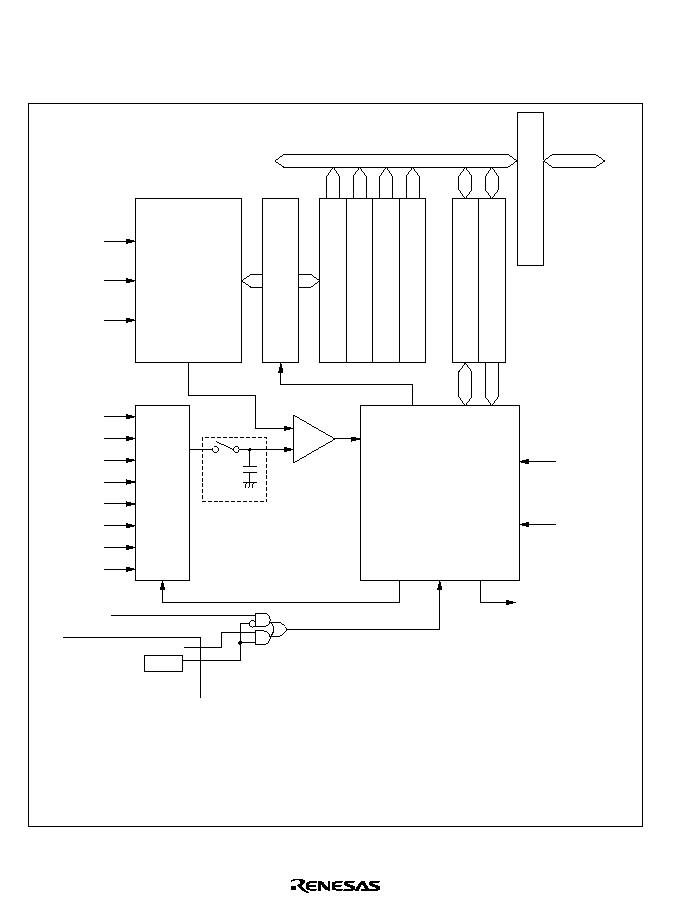
544
15.1.2
Block Diagram
Figure 15.1 shows a block diagram of the A/D converter.
Module data bus
Bus interf
ace
Internal
data bus
ADDRA
ADDRB
ADDRC
ADDRD
ADCSR
ADCR
Successiv
e-
appro
ximations register
10-bit D/A
Analog
multi-
plexer
Sample-and-
hold circuit
Comparator
+
�
Control circuit
�/4
�/8
ADI
interrupt signal
AV
V
AV
CC
REF
SS
AN
AN
AN
AN
AN
AN
AN
AN
0
1
2
3
4
5
6
7
Legend
ADCR:
ADCSR:
ADDRA:
ADDRB:
ADDRC:
ADDRD:
A/D control register
A/D control/status register
A/D data register A
A/D data register B
A/D data register C
A/D data register D
ADTRG
ADTE
Compare match A0
TCSR0
8-bit timer
Figure 15.1 A/D Converter Block Diagram

545
15.1.3
Input Pins
Table 15.1 summarizes the A/D converter's input pins. The eight analog input pins are divided
into two groups: group 0 (AN
0
to AN
3
), and group 1 (AN
4
to AN
7
). AV
CC
and AV
SS
are the power
supply for the analog circuits in the A/D converter. V
REF
is the A/D conversion reference voltage.
Table 15.1
A/D Converter Pins
Pin Name
Abbrevi-
ation
I/O
Function
Analog power supply pin
AV
CC
Input
Analog power supply
Analog ground pin
AV
SS
Input
Analog ground and reference voltage
Reference voltage pin
V
REF
Input
Analog reference voltage
Analog input pin 0
AN
0
Input
Group 0 analog inputs
Analog input pin 1
AN
1
Input
Analog input pin 2
AN
2
Input
Analog input pin 3
AN
3
Input
Analog input pin 4
AN
4
Input
Group 1 analog inputs
Analog input pin 5
AN
5
Input
Analog input pin 6
AN
6
Input
Analog input pin 7
AN
7
Input
A/D external trigger input pin
ADTRG
Input
External trigger input for starting A/D conversion

546
15.1.4
Register Configuration
Table 15.2 summarizes the A/D converter's registers.
Table 15.2
A/D Converter Registers
Address
*
1
Name
Abbreviation
R/W
Initial Value
H'FFFE0
A/D data register A H
ADDRAH
R
H'00
H'FFFE1
A/D data register A L
ADDRAL
R
H'00
H'FFFE2
A/D data register B H
ADDRBH
R
H'00
H'FFFE3
A/D data register B L
ADDRBL
R
H'00
H'FFFE4
A/D data register C H
ADDRCH
R
H'00
H'FFFE5
A/D data register C L
ADDRCL
R
H'00
H'FFFE6
A/D data register D H
ADDRDH
R
H'00
H'FFFE7
A/D data register D L
ADDRDL
R
H'00
H'FFFE8
A/D control/status register
ADCSR
R/(W)
*
2
H'00
H'FFFE9
A/D control register
ADCR
R/W
H'7E
Notes:
*
1 Lower 20 bits of the address in advanced mode.
*
2 Only 0 can be written in bit 7, to clear the flag.

547
15.2
Register Descriptions
15.2.1
A/D Data Registers A to D (ADDRA to ADDRD)
Bit
ADDRn
Initial value
14
AD8
0
R
12
AD6
0
R
10
AD4
0
R
8
AD2
0
R
6
AD0
0
R
0
--
0
R
4
--
0
R
2
--
0
R
15
AD9
0
R
13
AD7
0
R
11
AD5
0
R
9
AD3
0
R
7
AD1
0
R
1
--
0
R
5
--
0
R
3
--
0
R
A/D conversion data
10-bit data giving an
A/D conversion result
Reserved bits
Read/Write
(n = A to D)
The four A/D data registers (ADDRA to ADDRD) are 16-bit read-only registers that store the
results of A/D conversion.
An A/D conversion produces 10-bit data, which is transferred for storage into the A/D data
register corresponding to the selected channel. The upper 8 bits of the result are stored in the upper
byte of the A/D data register. The lower 2 bits are stored in the lower byte. Bits 5 to 0 of an A/D
data register are reserved bits that are always read as 0. Table 15.3 indicates the pairings of analog
input channels and A/D data registers.
The CPU can always read and write the A/D data registers. The upper byte can be read directly,
but the lower byte is read through a temporary register (TEMP). For details see section 15.3, CPU
Interface.
The A/D data registers are initialized to H'0000 by a reset and in standby mode.
Table 15.3
Analog Input Channels and A/D Data Registers
Analog Input Channel
Group 0
Group 1
A/D Data Register
AN
0
AN
4
ADDRA
AN
1
AN
5
ADDRB
AN
2
AN
6
ADDRC
AN
3
AN
7
ADDRD

548
15.2.2
A/D Control/Status Register (ADCSR)
Bit
Initial value
Read/Write
7
ADF
0
R/(W)
6
ADIE
0
R/W
5
ADST
0
R/W
4
SCAN
0
R/W
3
CKS
0
R/W
0
CH0
0
R/W
2
CH2
0
R/W
1
CH1
0
R/W
*
Note: Only 0 can be written, to clear the flag.
*
A/D end flag
Indicates end of A/D conversion
A/D interrupt enable
Enables and disables A/D end interrupts
A/D start
Starts or stops A/D conversion
Scan mode
Selects single mode or scan mode
Clock select
Selects the A/D conversion time
Channel select 2 to 0
These bits select analog
input channels
ADCSR is an 8-bit readable/writable register that selects the mode and controls the A/D converter.
ADCSR is initialized to H'00 by a reset and in standby mode.

549
Bit 7--A/D End Flag (ADF): Indicates the end of A/D conversion.
Bit 7
ADF
Description
0
[Clearing condition]
Read ADF when ADF =1, then write 0 in ADF.
DMAC activated by ADI interrupt.
(Initial value)
1
[Setting conditions]
Single mode: A/D conversion ends
Scan mode: A/D conversion ends in all selected channels
Bit 6--A/D Interrupt Enable (ADIE): Enables or disables the interrupt (ADI) requested at the
end of A/D conversion.
Bit 6
ADIE
Description
0
A/D end interrupt request (ADI) is disabled
(Initial value)
1
A/D end interrupt request (ADI) is enabled
Bit 5--A/D Start (ADST): Starts or stops A/D conversion. The ADST bit remains set to 1 during
A/D conversion. It can also be set to 1 by external trigger input at the
ADTRG pin, or by an 8-bit
timer compare match.
Bit 5
ADST
Description
0
A/D conversion is stopped
(Initial value)
1
Single mode: A/D conversion starts; ADST is automatically cleared to 0 when
conversion ends.
Scan mode: A/D conversion starts and continues, cycling among the selected
channels, until ADST is cleared to 0 by software, by a reset, or by a transition to
standby mode.

550
Bit 4--Scan Mode (SCAN): Selects single mode or scan mode. For further information on
operation in these modes, see section 15.4, Operation. Clear the ADST bit to 0 before switching
the conversion mode.
Bit 4
SCAN
Description
0
Single mode
(Initial value)
1
Scan mode
Bit 3--Clock Select (CKS): Selects the A/D conversion time. Clear the ADST bit to 0 before
switching the conversion time.
Bit 3
CKS
Description
0
Conversion time = 134 states (maximum)
(Initial value)
1
Conversion time = 70 states (maximum)
Bits 2 to 0--Channel Select 2 to 0 (CH2 to CH0): These bits and the SCAN bit select the analog
input channels. Clear the ADST bit to 0 before changing the channel selection.
Group
Selection
Channel Selection
Description
CH2
CH1
CH0
Single Mode
Scan Mode
0
0
0
AN
0
(Initial value)
AN
0
1
AN
1
AN
0
, AN
1
1
0
AN
2
AN
0
to AN
2
1
AN
3
AN
0
to AN
3
1
0
0
AN
4
AN
4
1
AN
5
AN
4
, AN
5
1
0
AN
6
AN
4
to AN
6
1
AN
7
AN
4
to AN
7

551
15.2.3
A/D Control Register (ADCR)
Bit
Initial value
Read/Write
7
TRGE
0
R/W
6
--
1
--
5
--
1
--
4
--
1
--
3
--
1
--
0
--
0
R/W
2
--
1
--
1
--
1
--
Trigger enable
Enables or disables starting of A/D conversion
by an external trigger or 8-bit timer compare match
Reserved bits
ADCR is an 8-bit readable/writable register that enables or disables starting of A/D conversion by
external trigger input or an 8-bit timer compare match signal. ADCR is initialized to H'7F by a
reset and in standby mode.
Bit 7--Trigger Enable (TRGE): Enables or disables starting of A/D conversion by an external
trigger or 8-bit timer compare match.
Bit 7
TRGE
Description
0
Starting of A/D conversion by an external trigger or 8-bit timer
compare match is disabled
(Initial value)
1
A/D conversion is started at the falling edge of the external trigger
signal (
ADTRG
) or by an 8-bit timer compare match
External trigger pin and 8-bit timer selection are performed by the 8-bit timer. For details, see
section 10, 8-Bit Timers.
Bits 6 to 1--Reserved: These bits cannot be modified and are always read as 1.
Bit 0--Reserved:
This bit can be read or written, but must not be set to 1.
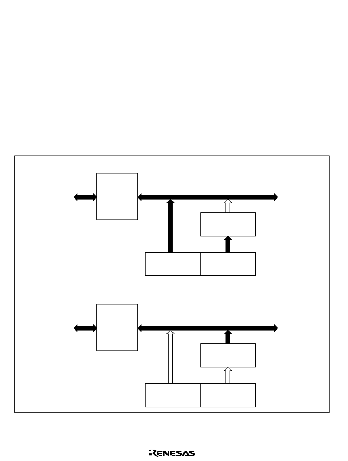
552
15.3
CPU Interface
ADDRA to ADDRD are 16-bit registers, but they are connected to the CPU by an 8-bit data bus.
Therefore, although the upper byte can be be accessed directly by the CPU, the lower byte is read
through an 8-bit temporary register (TEMP).
An A/D data register is read as follows. When the upper byte is read, the upper-byte value is
transferred directly to the CPU and the lower-byte value is transferred into TEMP. Next, when the
lower byte is read, the TEMP contents are transferred to the CPU.
When reading an A/D data register, always read the upper byte before the lower byte. It is possible
to read only the upper byte, but if only the lower byte is read, incorrect data may be obtained.
Figure 15.2 shows the data flow for access to an A/D data register.
Upper-byte read
Bus interface
Module data bus
CPU
(H'AA)
ADDRnH
(H'AA)
ADDRnL
(H'40)
Lower-byte read
Bus interface
Module data bus
CPU
(H'40)
ADDRnH
(H'AA)
ADDRnL
(H'40)
TEMP
(H'40)
TEMP
(H'40)
(n = A to D)
(n = A to D)
Figure 15.2 A/D Data Register Access Operation (Reading H'AA40)

553
15.4
Operation
The A/D converter operates by successive approximations with 10-bit resolution. It has two
operating modes: single mode and scan mode.
15.4.1
Single Mode (SCAN = 0)
Single mode should be selected when only one A/D conversion on one channel is required. A/D
conversion starts when the ADST bit is set to 1 by software, or by external trigger input. The
ADST bit remains set to 1 during A/D conversion and is automatically cleared to 0 when
conversion ends.
When conversion ends the ADF bit is set to 1. If the ADIE bit is also set to 1, an ADI interrupt is
requested at this time. To clear the ADF flag to 0, first read ADCSR, then write 0 in ADF.
When the mode or analog input channel must be switched during analog conversion, to prevent
incorrect operation, first clear the ADST bit to 0 in ADCSR to halt A/D conversion. After making
the necessary changes, set the ADST bit to 1 to start A/D conversion again. The ADST bit can be
set at the same time as the mode or channel is changed.
Typical operations when channel 1 (AN
1
) is selected in single mode are described next.
Figure 15.3 shows a timing diagram for this example.
1. Single mode is selected (SCAN = 0), input channel AN
1
is selected (CH2 = CH1 = 0,
CH0 = 1), the A/D interrupt is enabled (ADIE = 1), and A/D conversion is started
(ADST = 1).
2. When A/D conversion is completed, the result is transferred into ADDRB. At the same time
the ADF flag is set to 1, the ADST bit is cleared to 0, and the A/D converter becomes idle.
3. Since ADF = 1 and ADIE = 1, an ADI interrupt is requested.
4. The A/D interrupt handling routine starts.
5. The routine reads ADCSR, then writes 0 in the ADF flag.
6. The routine reads and processes the conversion result (ADDRB).
7. Execution of the A/D interrupt handling routine ends. After that, if the ADST bit is set to 1,
A/D conversion starts again and steps 2 to 7 are repeated.
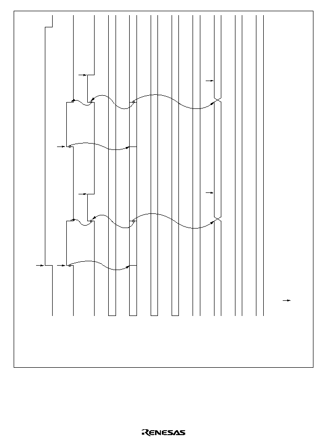
554
ADIE
ADST
ADF
State of channel 0
(AN )
Set
Set
Set
Clear
Clear
Idle
Idle
Idle
Idle
A/D conversion (1)
A/D conversion (2)
Idle
Read conversion result
A/D conversion result (1)
Read conversion result
A/D conversion result (2)
Note:
*
Vertical arrows ( ) indicate instructions executed by software.
0
1
2
3
A/D conversion
starts
*
*
*
*
*
ADDRA
ADDRB
ADDRC
ADDRD
State of channel 1
(AN )
State of channel 2
(AN )
State of channel 3
(AN )
Idle
Figure 15.3 Example of A/D Converter Operation (Single Mode, Channel 1 Selected)

555
15.4.2
Scan Mode (SCAN = 1)
Scan mode is useful for monitoring analog inputs in a group of one or more channels. When the
ADST bit is set to 1 by software or external trigger input, A/D conversion starts on the first
channel in the group (AN
0
when CH2 = 0, AN
4
when CH2 = 1). When two or more channels are
selected, after conversion of the first channel ends, conversion of the second channel (AN
1
or
AN
5
) starts immediately. A/D conversion continues cyclically on the selected channels until the
ADST bit is cleared to 0. The conversion results are transferred for storage into the A/D data
registers corresponding to the channels.
When the mode or analog input channel selection must be changed during analog conversion, to
prevent incorrect operation, first clear the ADST bit to 0 in ADCSR to halt A/D conversion. After
making the necessary changes, set the ADST bit to 1. A/D conversion will start again from the
first channel in the group. The ADST bit can be set at the same time as the mode or channel
selection is changed.
Typical operations when three channels in group 0 (AN
0
to AN
2
) are selected in scan mode are
described next. Figure 15.4 shows a timing diagram for this example.
1. Scan mode is selected (SCAN = 1), scan group 0 is selected (CH2 = 0), analog input channels
AN
0
to AN
2
are selected (CH1 = 1, CH0 = 0), and A/D conversion is started (ADST = 1).
2. When A/D conversion of the first channel (AN
0
) is completed, the result is transferred into
ADDRA. Next, conversion of the second channel (AN
1
) starts automatically.
3. Conversion proceeds in the same way through the third channel (AN
2
).
4. When conversion of all selected channels (AN
0
to AN
2
) is completed, the ADF flag is set to 1
and conversion of the first channel (AN
0
) starts again. If the ADIE bit is set to 1, an ADI
interrupt is requested at this time.
5. Steps 2 to 4 are repeated as long as the ADST bit remains set to 1. When the ADST bit is
cleared to 0, A/D conversion stops. After that, if the ADST bit is set to 1, A/D conversion
starts again from the first channel (AN
0
).
556
ADST
ADF
State of channel 0
(AN )
0
1
2
3
Continuous A/D conversion
Set
Clear
*
1
Clear
*
1
Idle
A/D conversion (1)
Idle
Idle
Idle
A/D conversion (4)
Idle
A/D conversion (2)
Idle
A/D conversion (5)
Idle
A/D conversion (3)
Idle
Idle
Transfer
A/D conversion result (1)
A/D conversion result (4)
A/D conversion result (2)
A/D conversion result (3)
*
1
*
2
A/D conversion time
Notes:
*
2
*
1
ADDRA
ADDRB
ADDRC
ADDRD
State of channel 1
(AN )
State of channel 2
(AN )
State of channel 3
(AN )
Vertical arrows ( ) indicate instructions executed by software.
Data currently being converted is ignored.
Figure 15.4 Example of A/D Converter Operation (Scan Mode,
Channels AN
0
to AN
2
Selected)
557
15.4.3
Input Sampling and A/D Conversion Time
The A/D converter has a built-in sample-and-hold circuit. The A/D converter samples the analog
input at a time t
D
after the ADST bit is set to 1, then starts conversion. Figure 15.5 shows the A/D
conversion timing. Table 15.4 indicates the A/D conversion time.
As indicated in figure 15.5, the A/D conversion time includes t
D
and the input sampling time. The
length of t
D
varies depending on the timing of the write access to ADCSR. The total conversion
time therefore varies within the ranges indicated in table 15.4.
In scan mode, the values given in table 15.4 apply to the first conversion. In the second and
subsequent conversions the conversion time is fixed at 128 states when CKS = 0 or 66 states when
CKS = 1.
Address bus
Write signal
Input sampling
timing
ADF
(1)
(2)
t
D
t
SPL
t
CONV
Legend
(1):
(2):
t :
t :
t :
D
SPL
CONV
ADCSR write cycle
ADCSR address
A/D conversion start delay time
Input sampling time
A/D conversion time
Figure 15.5 A/D Conversion Timing
558
Table 15.4
A/D Conversion Time (Single Mode)
CKS = 0
CKS = 1
Symbol
Min
Typ
Max
Min
Typ
Max
Synchronization delay
t
D
6
--
9
4
--
5
Input sampling time
t
SPL
--
31
--
--
15
--
A/D conversion time
t
CONV
131
--
134
69
--
70
Note:
Values in the table are numbers of states.
15.4.4
External Trigger Input Timing
A/D conversion can be externally triggered. When the TRGE bit is set to 1 in ADCR and the 8-bit
timer's ADTE bit is cleared to 0, external trigger input is enabled at the
ADTRG pin. A high-to-
low transition at the
ADTRG pin sets the ADST bit to 1 in ADCSR, starting A/D conversion.
Other operations, in both single and scan modes, are the same as if the ADST bit had been set to 1
by software. Figure 15.6 shows the timing.
ADTRG
Internal trigger
signal
ADST
A/D conversion
Figure 15.6 External Trigger Input Timing

559
15.5
Interrupts
The A/D converter generates an interrupt (ADI) at the end of A/D conversion. The ADI interrupt
request can be enabled or disabled by the ADIE bit in ADCSR. The ADI interrupt request can be
designated as a DMAC activation source. In this case, an interrupt request is not sent to the CPU.
15.6
Usage Notes
When using the A/D converter, note the following points:
1. Analog Input Voltage Range: During A/D conversion, the voltages input to the analog input
pins should be in the range AV
SS
AN
n
V
REF
.
2. Relationships of AV
CC
and AV
SS
to V
CC
and V
SS
: AV
CC
, AV
SS
, V
CC
, and V
SS
should be related
as follows: AV
SS
= V
SS
. AV
CC
and AV
SS
must not be left open, even if the A/D converter is not
used.
3. V
REF
Programming Range: The reference voltage input at the V
REF
pin should be in the range
V
REF
AV
CC
.
4. Note on Board Design: In board layout, separate the digital circuits from the analog circuits as
much as possible. Particularly avoid layouts in which the signal lines of digital circuits cross or
closely approach the signal lines of analog circuits. Induction and other effects may cause the
analog circuits to operate incorrectly, or may adversely affect the accuracy of A/D conversion.
The analog input signals (AN
0
to AN
7
), analog reference voltage (V
REF
), and analog supply
voltage (AV
CC
) must be separated from digital circuits by the analog ground (AV
SS
). The
analog ground (AV
SS
) should be connected to a stable digital ground (V
SS
) at one point on the
board.
5. Note on Noise: To prevent damage from surges and other abnormal voltages at the analog
input pins (AN
0
to AN
7
) and analog reference voltage pin (V
REF
), connect a protection circuit
like the one in figure 15.7 between AV
CC
and AV
SS
. The bypass capacitors connected to AV
CC
and V
REF
and the filter capacitors connected to AN
0
to AN
7
must be connected to AV
SS
. If filter
capacitors like the ones in figure 15.7 are connected, the voltage values input to the analog
input pins (AN
0
to AN
7
) will be smoothed, which may give rise to error. Error can also occur if
A/D conversion is frequently performed in scan mode so that the current that charges and
discharges the capacitor in the sample-and-hold circuit of the A/D converter becomes greater
than that input to the analog input pins via input impedance Rin. The circuit constants should
therefore be selected carefully.
560
AV
CC
*
1
*
1
V
REF
AN
0
to AN
7
AV
SS
Notes:
*
1
*
2 Rin: input impedance
Rin
*
2
100
0.1
�
F
0.01
�
F
10
�
F
Figure 15.7 Example of Analog Input Protection Circuit
Table 15.5
Analog Input Pin Ratings
Item
min
max
Unit
Analog input capacitance
--
20
pF
Allowable signal-source impedance
--
10
*
k
Note:
*
When conversion time = 134 states, V
CC
= 4.5 V to 5.5 V, and �
13 Mhz. For details see
section 21, Electrical Characteristics.
20 pF
To A/D converter
AN
0
to AN
7
10 k
Figure 15.8 Analog Input Pin Equivalent Circuit
Note:
Numeric values are approximate, except in table 15.5
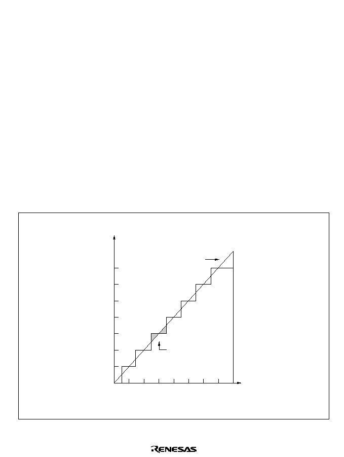
561
6. A/D Conversion Accuracy Definitions: A/D conversion accuracy in the H8/3069F is defined as
follows:
�
Resolution:....................Digital output code length of A/D converter
�
Offset error: ..................Deviation from ideal A/D conversion characteristic of analog input
voltage required to raise digital output from minimum voltage value
0000000000 to 0000000001 (figure 15.10)
�
Full-scale error:.............Deviation from ideal A/D conversion characteristic of analog input
voltage required to raise digital output from 1111111110 to
1111111111 (figure 15.10)
�
Quantization error:........Intrinsic error of the A/D converter; 1/2 LSB (figure 15.9)
�
Nonlinearity error: ........Deviation from ideal A/D conversion characteristic in range from zero
volts to full scale, exclusive of offset error, full-scale error, and
quantization error.
�
Absolute accuracy:........Deviation of digital value from analog input value, including offset
error, full-scale error, quantization error, and nonlinearity error.
111
110
101
100
011
010
001
000
1/8 2/8 3/8 4/8 5/8 6/8 7/8 FS
Quantization error
Analog input
voltage
Digital
output
Ideal A/D conversion
characteristic
Figure 15.9 A/D Converter Accuracy Definitions (1)
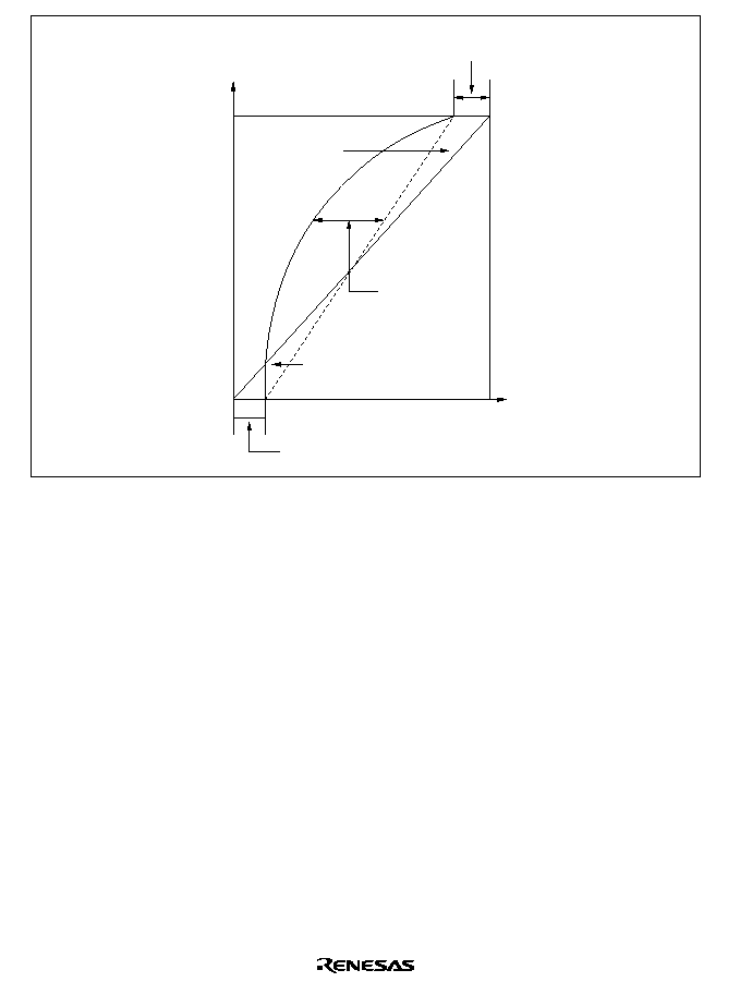
562
FS
Offset error
Nonlinearity
error
Actual A/D conversion
characteristic
Analog input
voltage
Digital
output
Ideal A/D
conversion
characteristic
Full-scale
error
Figure 15.10 A/D Converter Accuracy Definitions (2)
7. Allowable Signal-Source Impedance: The analog inputs of the H8/3069F are designed to
assure accurate conversion of input signals with a signal-source impedance not exceeding 10
k
. The reason for this rating is that it enables the input capacitor in the sample-and-hold
circuit in the A/D converter to charge within the sampling time. If the sensor output impedance
exceeds 10 k
, charging may be inadequate and the accuracy of A/D conversion cannot be
guaranteed.
If a large external capacitor is provided in single mode, then the internal 10-k
input resistance
becomes the only significant load on the input. In this case the impedance of the signal source
is not a problem.
A large external capacitor, however, acts as a low-pass filter. This may make it impossible to
track analog signals with high dv/dt (e.g. a variation of 5 mV/
�
s) (figure 15.11). To convert
high-speed analog signals or to use scan mode, insert a low-impedance buffer.
8. Effect on Absolute Accuracy: Attaching an external capacitor creates a coupling with ground,
so if there is noise on the ground line, it may degrade absolute accuracy. The capacitor must be
connected to an electrically stable ground, such as AV
SS
.
If a filter circuit is used, be careful of interference with digital signals on the same board, and
make sure the circuit does not act as an antenna.
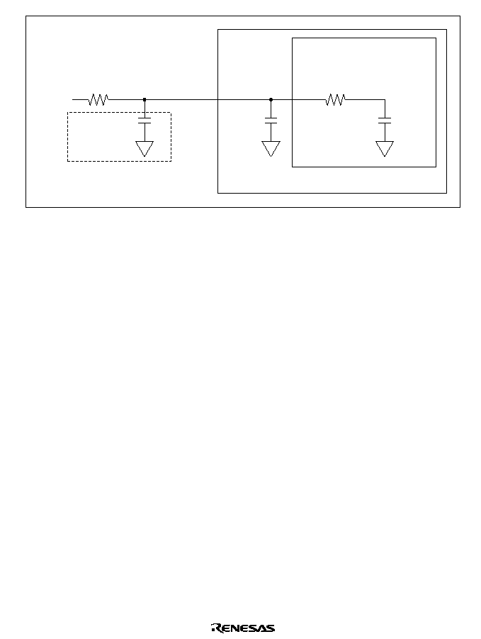
563
Equivalent circuit of
A/D converter
H8/3069F
20 pF
Cin =
15 pF
10 k
Up to 10 k
Low-pass
filter C
Up to 0.1
�
F
Sensor output impedance
Sensor
input
Figure 15.11 Analog Input Circuit (Example)

564
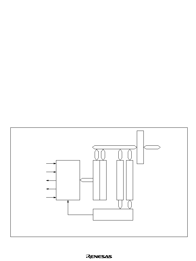
565
Section 16 D/A Converter
16.1
Overview
The H8/3069F includes a D/A converter with two channels.
16.1.1
Features
D/A converter features are listed below.
�
Eight-bit resolution
�
Two output channels
�
Conversion time: maximum 10
�
s (with 20-pF capacitive load)
�
Output voltage: 0 V to V
REF
�
D/A outputs can be sustained in software standby mode
16.1.2
Block Diagram
Figure 16.1 shows a block diagram of the D/A converter.
D
ADR0
D
ADR1
DA
C
R
D
ASTCR
V
AV
DA
DA
AV
REF
CC
SS
0
1
Legend
DACR:
DADR0:
DADR1:
DASTCR:
8-bit D/A
Module data bus
Bus interf
ace
Internal
data bus
Control circuit
D/A control register
D/A data register 0
D/A data register 1
D/A standby control register
Figure 16.1 D/A Converter Block Diagram

566
16.1.3
Input/Output Pins
Table 16.1 summarizes the D/A converter's input and output pins.
Table 16.1
D/A Converter Pins
Pin Name
Abbreviation I/O
Function
Analog power supply pin
AV
CC
Input
Analog power supply and reference voltage
Analog ground pin
AV
SS
Input
Analog ground and reference voltage
Analog output pin 0
DA
0
Output
Analog output, channel 0
Analog output pin 1
DA
1
Output
Analog output, channel 1
Reference voltage input pin
V
REF
Input
Analog reference voltage
16.1.4
Register Configuration
Table 16.2 summarizes the D/A converter's registers.
Table 16.2
D/A Converter Registers
Address
*
Name
Abbreviation
R/W
Initial Value
H'FFF9C
D/A data register 0
DADR0
R/W
H'00
H'FFF9D
D/A data register 1
DADR1
R/W
H'00
H'FFF9E
D/A control register
DACR
R/W
H'1F
H'EE01A
D/A standby control register
DASTCR
R/W
H'FE
Note:
*
Lower 20 bits of the address in advanced mode.
567
16.2
Register Descriptions
16.2.1
D/A Data Registers 0 and 1 (DADR0/1)
Bit
Initial value
Read/Write
7
0
R/W
6
0
R/W
5
0
R/W
4
0
R/W
3
0
R/W
2
0
R/W
1
0
R/W
0
0
R/W
The D/A data registers (DADR0 and DADR1) are 8-bit readable/writable registers that store the
data to be converted. When analog output is enabled, the D/A data register values are constantly
converted and output at the analog output pins.
The D/A data registers are initialized to H'00 by a reset and in standby mode.
When the DASTE bit is set to 1 in the D/A standby control register (DASTCR), the D/A registers
are not initialized in software standby mode.
16.2.2
D/A Control Register (DACR)
Bit
Initial value
Read/Write
7
DAOE1
0
R/W
6
DAOE0
0
R/W
5
DAE
0
R/W
4
--
1
--
3
--
1
--
2
--
1
--
1
--
1
--
0
--
1
--
D/A output enable 1
D/A output enable 0
D/A enable
Controls D/A conversion and analog output
Controls D/A conversion and analog output
Controls D/A conversion
DACR is an 8-bit readable/writable register that controls the operation of the D/A converter.
DACR is initialized to H'1F by a reset and in standby mode.
When the DASTE bit is set to 1 in DASTCR, the DACR is not initialized in software standby
mode.

568
Bit 7--D/A Output Enable 1 (DAOE1): Controls D/A conversion and analog output.
Bit 7
DAOE1
Description
0
DA
1
analog output is disabled
1
Channel-1 D/A conversion and DA
1
analog output are enabled
Bit 6--D/A Output Enable 0 (DAOE0): Controls D/A conversion and analog output.
Bit 6
DAOE0
Description
0
DA
0
analog output is disabled
1
Channel-0 D/A conversion and DA
0
analog output are enabled
Bit 5--D/A Enable (DAE): Controls D/A conversion, together with bits DAOE0 and DAOE1.
When the DAE bit is cleared to 0, analog conversion is controlled independently in channels 0
and 1. When the DAE bit is set to 1, analog conversion is controlled together in channels 0 and 1.
Output of the conversion results is always controlled independently by DAOE0 and DAOE1.
Bit 7
DAOE1
Bit 6
DAOE0
Bit 5
DAE
Description
0
0
--
D/A conversion is disabled in channels 0 and 1
1
0
D/A conversion is enabled in channel 0
D/A conversion is disabled in channel 1
1
D/A conversion is enabled in channels 0 and 1
1
0
0
D/A conversion is disabled in channel 0
D/A conversion is enabled in channel 1
1
D/A conversion is enabled in channels 0 and 1
1
--
D/A conversion is enabled in channels 0 and 1
When the DAE bit is set to 1, even if bits DAOE0 and DAOE1 in DACR and the ADST bit in
ADCSR are cleared to 0, the same current is drawn from the analog power supply as during A/D
and D/A conversion.
Bits 4 to 0--Reserved: These bits cannot be modified and are always read as 1.
569
16.2.3
D/A Standby Control Register (DASTCR)
DASTCR is an 8-bit readable/writable register that enables or disables D/A output in software
standby mode.
Bit
Initial value
Read/Write
7
--
1
--
6
--
1
--
5
--
1
--
4
--
1
--
3
--
1
--
0
DASTE
0
R/W
2
--
1
--
1
--
1
--
Reserved bits
D/A standby enable
Enables or disables D/A output
in software standby mode
DASTCR is initialized to H'FE by a reset and in hardware standby mode. It is not initialized in
software standby mode.
Bits 7 to 1--Reserved: These bits cannot be modified and are always read as 1.
Bit 0--D/A Standby Enable (DASTE): Enables or disables D/A output in software standby
mode.
Bit 0
DASTE
Description
0
D/A output is disabled in software standby mode
(Initial value)
1
D/A output is enabled in software standby mode

570
16.3
Operation
The D/A converter has two built-in D/A conversion circuits that can perform conversion
independently.
D/A conversion is performed constantly while enabled in DACR. If the DADR0 or DADR1 value
is modified, conversion of the new data begins immediately. The conversion results are output
when bits DAOE0 and DAOE1 are set to 1.
An example of D/A conversion on channel 0 is given next. Timing is indicated in figure 16.2.
1. Data to be converted is written in DADR0.
2. Bit DAOE0 is set to 1 in DACR. D/A conversion starts and DA0 becomes an output pin. The
converted result is output after the conversion time.
�
V
REF
The output value is
DADR contents
256
Output of this conversion result continues until the value in DADR0 is modified or the DAOE0
bit is cleared to 0.
3. If the DADR0 value is modified, conversion starts immediately, and the result is output after
the conversion time.
4. When the DAOE0 bit is cleared to 0, DA0 becomes an input pin.
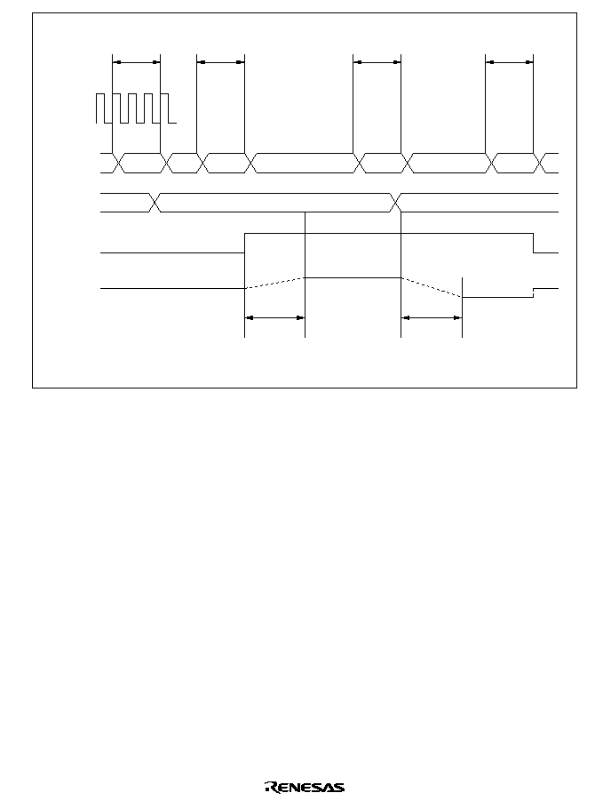
571
DADR0
write cycle
DACR
write cycle
DADR0
write cycle
DACR
write cycle
Address
DADR0
DAOE0
DA
0
Conversion data 1
Conversion data 2
High-impedance state
Conversion
result 1
Conversion
result 2
t
DCONV
t
DCONV
Legend
t : D/A conversion time
DCONV
Figure 16.2 Example of D/A Converter Operation
16.4
D/A Output Control
In the H8/3069F, D/A converter output can be enabled or disabled in software standby mode.
When the DASTE bit is set to 1 in DASTCR, D/A converter output is enabled in software standby
mode. The D/A converter registers retain the values they held prior to the transition to software
standby mode.
When D/A output is enabled in software standby mode, the reference supply current is the same as
during normal operation.

572
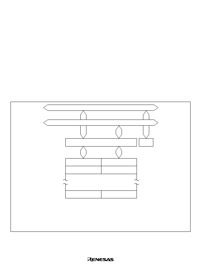
573
Section 17 RAM
17.1
Overview
The H8/3069F has 16 kbytes RAM. The RAM is connected to the CPU by a 16-bit data bus. The
CPU accesses both byte data and word data in two states, making the RAM useful for rapid data
transfer.
The on-chip RAM of the H8/3069F is assigned to addresses H'FBF20 to H'FFF1F in modes 1, 2,
and 7, and to addresses H'FFBF20 to H'FFFF1F in modes 3, 4, and 5. The RAM enable bit
(RAME) in the system control register (SYSCR) can enable or disable the on-chip RAM.
17.1.1
Block Diagram
Figure 17.1 shows a block diagram of the on-chip RAM.
H'FBF20
*
H'FBF22
*
H'FFF1E
*
H'FBF21
*
H'FBF23
*
H'FFF1F
*
On-chip data bus (upper 8 bits)
On-chip data bus (lower 8 bits)
Bus interface
SYSCR
On-chip RAM
Even addresses
Odd addresses
Legend
SYSCR: System control register
Note:
*
Lower 20 bits of the address in mode 7.
Figure 17.1 RAM Block Diagram
574
17.1.2
Register Configuration
The on-chip RAM is controlled by SYSCR. Table 17.1 gives the address and initial value of
SYSCR.
Table 17.1
System Control Register
Address
*
Name
Abbreviation
R/W
Initial Value
H'EE012
System control register
SYSCR
R/W
H'09
Note:
*
Lower 20 bits of the address in advanced mode.
17.2
System Control Register (SYSCR)
Bit
Initial value
Read/Write
7
SSBY
0
R/W
6
STS2
0
R/W
5
STS1
0
R/W
4
STS0
0
R/W
3
UE
1
R/W
2
NMIEG
0
R/W
1
SSOE
0
R/W
0
RAME
1
R/W
Software standby
Standby timer select 2 to 0
User bit enable
NMI edge select
Software standby
output port enable
RAM enable bit
Enables or disables
on-chip RAM
One function of SYSCR is to enable or disable access to the on-chip RAM. The on-chip RAM is
enabled or disabled by the RAME bit in SYSCR. For details about the other bits, see section 3.3,
System Control Register (SYSCR).
Bit 0--RAM Enable (RAME): Enables or disables the on-chip RAM. The RAME bit is
initialized at the rising edge of the input at the
RES pin. It is not initialized in software standby
mode.
Bit 0
RAME
Description
0
On-chip RAM is disabled
1
On-chip RAM is enabled
(Initial value)

575
17.3
Operation
When the RAME bit is set to 1, the on-chip RAM is enabled. Accesses to addresses H'FBF20 to
H'FFF1F in modes 1, 2, and 7, and to addresses H'FFBF20 to H'FFFF1F in the H8/3069F in
modes 3, 4, and 5, are directed to the on-chip RAM. In modes 1 to 5 (expanded modes), when the
RAME bit is cleared to 0, the off-chip address space is accessed. In mode 7 (single-chip mode),
when the RAME bit is cleared to 0, the on-chip RAM is not accessed: read access always results
in H'FF data, and write access is ignored.
Since the on-chip RAM is connected to the CPU by an internal 16-bit data bus, it can be written
and read by word access. It can also be written and read by byte access. Byte data is accessed in
two states using the upper 8 bits of the data bus. Word data starting at an even address is accessed
in two states using all 16 bits of the data bus.

576

577
Section 18 ROM
18.1
Features
This LSI has an on-chip 512-kbyte flash memory. The flash memory has the following features.
�
Two flash-memory MATs according to LSI initiation mode
The on-chip flash memory has two memory spaces in the same address space (hereafter
referred to as memory MATs). The mode setting in the initiation determines which memory
MAT is initiated first. The MAT can be switched by using the bank-switching method after
initiation.
The user memory MAT is initiated at a power-on reset in user mode: 512 kbytes
The user boot memory MAT is initiated at a power-on reset in user boot mode:8 kbytes
�
Three on-board programming modes and one off-board programming mode
On-board programming modes
Boot mode: This mode is a program mode that uses an on-chip SCI interface. The user MAT and
user boot MAT can be programmed. This mode can automatically adjust the bit rate between host
and this LSI.
User program mode: The user MAT can be programmed by using the optional interface.
User boot mode: The user boot program of the optional interface can be made and the user MAT
can be programmed.
Off-board programming mode
PROM mode: This mode uses the PROM programmer. The user MAT and user boot MAT can be
programmed.
�
Programming/erasing interface by the download of on-chip program
This LSI has a dedicated programming/erasing program. After downloading this program to
the on-chip RAM, programming/erasing can be performed by setting the argument parameter.
User branch*
The program processing is performed in 128-byte units. It consists the program pulse application,
verify read, and several other steps. Erasing is performed in one divided-block units and consists
of several steps. The user processing routine can be executed between the steps, this setting for
which is called the user branch addition.
Note: *
Not available in the H8/3069F.

578
�
Emulation function of flash memory by using the on-chip RAM
As flash memory is overlapped with part of the on-chip RAM, the flash memory programming
can be emulated in real time.
�
Protection modes
There are two protection modes: software protection by the register setting and hardware
protection by the FWE pin. The protection state for flash memory programming/erasing can be
set.
When abnormalities, such as runaway of programming/erasing are detected, these modes enter
the error protection state and the programming/erasing processing is suspended.
�
Programming/erasing time
The flash memory programming time is 3ms (typ) in 128-byte simultaneous programming and
25
�
s per byte. The erasing time is 1000ms (typ) per block.
�
Number of programming
The number of flash memory programming can be up to minimum 100 times.
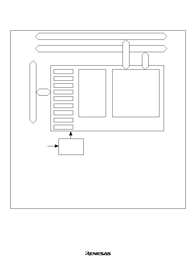
579
18.2
Overview
18.2.1
Block Diagram
FCCS
FPCS
FECS
FKEY
FMATS
FTDAR
RAMCR
FVACR
FVADR
Control unit
Memory MAT unit
Flash memory
User MAT: 512 kbytes
User boot MAT: 8 kbytes
Operating
mode
Module bus
FWE pin
Mode pin
Internal address bus
Internal data bus (16 bits)
Legend
FCCS:
Flash code control and status register
FPCS:
Flash program code select register
FECS:
Flash erase code select register
FKEY:
Flash key code register
FMATS: Flash MAT select register
FTDAR: Flash transfer destination address register
RAMCR: RAM control register
FVACR: Flash vector address control register
FVADR: Flash vector address data register
Figure 18. 1 Block Diagram of Flash Memory

580
18.2.2
Operating Mode
When each mode pin and the FWE pin are set in the reset state and reset start is performed, the
microcomputer enters each operating mode as shown in figure 18.2. For the setting of each mode
pin and the FWE pin, see table 18.1.
�
Flash memory cannot be read, programmed, or erased in ROM invalid mode.
�
Flash memory can be read in user mode, but cannot be programmed or erased.
�
Flash memory can be read, programmed, or erased on the board only in user program mode,
user boot mode, and boot mode.
�
Flash memory can be read, programmed, or erased by means of the PROM programmer in
PROM mode.
Reset state
ROM invalid
mode
PROM mode
User mode
User program
mode
User boot
mode
Boot mode
On-board programming mode
FWE=0
RAM emulation is enabled
FWE=1
RES
=0
ROM invalid
mode setting
RES
=0
User mode setting
RES
=0
User program
mode setting
User boot
mode setting
RES
=0
Boot mode setting
RES
=0
RES
=0
PROM mode setting
Figure 18.2 Mode Transition of Flash Memory

581
Table 18.1
Location of FWE and MD Pins and Operating Modes
Mode
Pin
Reset
state
On-chip
ROM
invalid
mode
*
On-chip
ROM
valid
mode
*
User
program
mode
User
boot
mode
Boot
mode
PROM
mode
RES
0
1
1
1
1
1
1
FWE
0/1
0
0
1
1
1
1
MD0
0/1
0/1
0
1
1
1
1
0
MD1
0/1
0/1
0
0/1
0/1
0/1
0/1
0
MD2
0/1
0
1
1
1
0
0
0
NMI
0/1
0/1
0/1
0/1
0
1
0/1
Note:
*
Modes 1 to 4 are on-chip ROM invalid modes.
Modes 5 and 7 are on-chip ROM valid modes. For details, see section 3, MCU Operating
Modes.
18.2.3
Mode Comparison
The comparison table of programming and erasing related items about boot mode, user program
mode, user boot mode, and PROM mode is shown in table 18.2.
582
Table 18.2
Comparison of Programming Modes
Boot mode
User program
mode
User boot mode
PROM mode
Programming/
Erasing
Environment
On-board
programming
On-board
programming
On-board
programming
Off-board
programming
Programming/
Erasing Enable
MAT
User MAT
User boot MAT
User MAT
User MAT
User MAT
User boot MAT
All Erasure
(Automatic)
(Automatic)
Block Division
Erasure
*
1
�
Program Data
Transfer
From host via
SCI
From optional
device via RAM
From optional
device via RAM
Via programmer
User Branch
Function
�
�
�
�
RAM Emulation
�
�
�
Reset Initiation
MAT
Embedded
program storage
MAT
User MAT
User boot MAT
*
2
--
Transition to
User Mode
Mode setting
change and reset
FWE setting
change
Mode setting
change and reset
--
Notes :
*
1 All-erasure is performed. After that, the specified block can be erased.
*
2 Initiation starts from the embedded program storage MAT. After checking the flash-
memory related registers, initiation starts from the reset vector of the user MAT.
�
The user boot MAT can be programmed or erased only in boot mode and PROM mode.
�
The user MAT and user boot MAT are erased in boot mode. Then, the user MAT and user boot
MAT can be programmed by means of the command method. However, the contents of the
MAT cannot be read until this state.
Only user boot MAT is programmed and the user MAT is programmed in user boot mode or
only user MAT is programmed because user boot mode is not used.
�
The boot operation of the optional interface can be performed by the mode pin setting different
from user program mode in user boot mode.
18.2.4
Flash MAT Configuration
This LSI's flash memory is configured by the 512-kbyte user MAT and 8-kbyte user boot MAT.
The start address is allocated to the same address in the user MAT and user boot MAT. Therefore,
when the program execution or data access is performed between two MATs, the MAT must be
switched by using FMATS.
583
The user MAT or user boot MAT can be read in all modes if it is in ROM valid mode. However,
the user boot MAT can be programmed only in boot mode and PROM mode.
<User MAT>
<User Boot MAT>
Address H'000000
Address H'07FFFF
Address H'000000
Address H'001FFF
512 kbytes
8 kbytes
Figure 18.3 Flash Memory Configuration
The user MAT and user boot MAT have different memory sizes. Do not access a user boot MAT
that is 8 kbytes or more. When a user boot MAT exceeding 8 kbytes is read from, an undefined
value is read.
18.2.5
Block Division
The user MAT is divided into 64 kbytes (seven blocks), 32 kbytes (one block), and 4 kbytes (eight
blocks) as shown in figure 18.4. The user MAT can be erased in this divided-block units and the
erase-block number of EB0 to EB15 is specified when erasing.
The RAM emulation can be performed in the eight blocks of 4 kbytes.
584
<User MAT>
Address H'000000
Address H'07FFFF
512 kbytes
4 kbytes
�
8
32 kbytes
64 kbytes
64 kbytes
64 kbytes
64 kbytes
64 kbytes
64 kbytes
64 kbytes
EB0
EB7
to
EB8
EB9
EB10
EB11
EB12
EB13
EB14
EB15
Erase block
Note:
*
The RAM emulation can be performed in the eight blocks of 4 kbytes.
*
Figure 18.4 Block Division of User MAT
18.2.6
Programming/Erasing Interface
Programming/erasing is executed by downloading the on-chip program to the on-chip RAM and
specifying the program address/data and erase block by using the interface register/parameter.
The procedure program is made by the user in user program mode and user boot mode. The
overview of the procedure is as follows. For details, see section 18.5.2, User Program Mode.
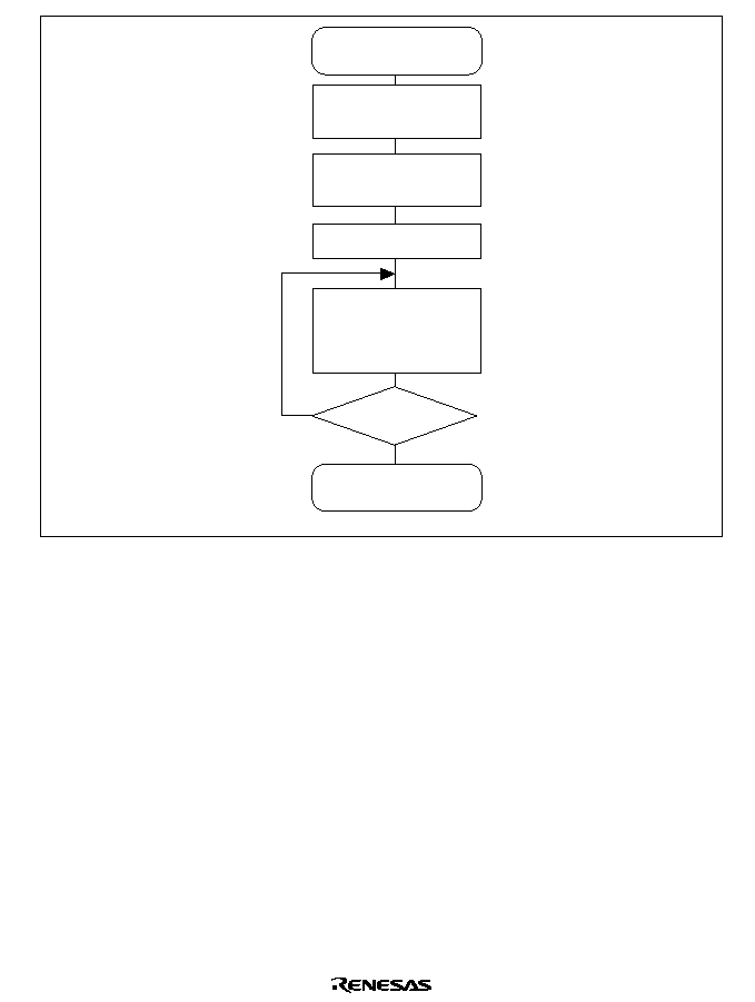
585
Download on-chip
program by setting
FKEY and the SCO bits
Initialization execution
(download program execution)
Select on-chip program
to be downloaded and
set download destination
Programming (in 128-byte
units) or erasing (in
one-block units)
(download program execution)
Start user procedure
program for
programming/erasing
End user procedure
program
Programming/erasing
completed?
No
Yes
Figure 18.5 Overview of User Procedure Program
1. Selection of on-chip program to be downloaded and setting of download destination
This LSI has programming/erasing programs and they can be downloaded to the on-chip RAM.
The on-chip program to be downloaded is selected by setting the corresponding bits in the
programming/erasing interface register. The download destination can be specified by FTDAR.
2. Download of on-chip program
The on-chip program is automatically downloaded by setting the SCO bit in the flash key code
register (FKEY) and the flash code control and status register (FCCS), which are programming/
erasing interface registers.
The user MAT is replaced to the embedded program storage area when downloading. Since the
flash memory cannot be read when programming/erasing, the procedure program, which is
working from download to completion of programming/erasing, must be executed in a space other
than the flash memory to be programmed/erased (for example, on-chip RAM).
Since the result of download is returned to the programming/erasing interface parameters, whether
the normal download is executed or not can be confirmed.

586
3. Initialization of programming/erasing
The operating frequency and user branch are set before execution of programming/erasing. The
user branch destination must be area other than the flash memory area or the area where the on-
chip program is downloaded. These settings are performed by using the programming/erasing
interface parameters.
4. Programming/erasing execution
To program or erase, the FWE pin must be set to 1 and user program mode must be entered.
The program data/programming destination address is specified in 128-byte units when
programming.
The block to be erased is specified in erase-block units when erasing.
These specifications are set by using the programming/erasing interface parameters and the on-
chip program is initiated. The on-chip program is executed by using the JSR or BSR instruction to
perform the subroutine call of the specified address in the on-chip RAM. The execution result is
returned to the programming/erasing interface parameters.
The area to be programmed must be erased in advance when programming flash memory.
All interrupts are prohibited during programming and erasing. Interrupts must not occur in the user
system.
5. When programming/erasing is executed consecutively
When the processing is not ended by the 128-byte programming or one-block erasure, the program
address/data and erase-block number must be updated and consecutive programming/erasing is
required.
Since the downloaded on-chip program is left in the on-chip RAM after the processing, download
and initialization are not required when the same processing is executed consecutively.

587
18.3
Pin Configuration
Flash memory is controlled by the pin as shown in table 18.3.
Table 18.3
Pin Configuration
Pin Name
Abbreviation
Input/Output
Function
Reset
RES
Input
Reset
Flash programming
enable
FWE
Input
Hardware protection when programming
flash memory
Mode 2
MD2
Input
Sets operating mode of this LSI
Mode 1
MD1
Input
Sets operating mode of this LSI
Mode 0
MD0
Input
Sets operating mode of this LSI
Non-maskable
interrupt
NMI
Input
Sets operating mode of this LSI
Transmit data
TxD1
Output
Serial transmit data output (used in boot
mode)
Receive data
RxD1
Input
Serial receive data input (used in boot
mode)
Note:
For the pin configuration in PROM mode, see section 18.9, PROM Mode.

588
18.4
Register Configuration
18.4.1
Registers
The registers/parameters which control flash memory when the on-chip flash memory is valid are
shown in table 18.4.
There are several operating modes for accessing flash memory, for example, read mode/program
mode.
There are two memory MATs: user MAT and user boot MAT. The dedicated registers/parameters
are allocated for each operating mode and MAT selection. The correspondence of operating modes
and registers/parameters for use is shown in table 18.5.

589
Table 18.4 (1)
Register Configuration
Name
Abbreviation
R/W
Initial
Value
Address
Access
Size
Flash code control status
register
FCCS
R, W
*
1
H'00
*
2
H'80
*
2
H'EE0B0
8
Flash program code select
register
FPCS
R/W
H'00
H'EE0B1
8
Flash erase code select
register
FECS
R/W
H'00
H'EE0B2
8
Flash key code register
FKEY
R/W
H'00
H'EE0B4
8
Flash MAT select register
FMATS
R/W
H'00
*
3
H'AA
*
3
H'EE0B5
8
Flash transfer destination
address register
FTDAR
R/W
H'00
H'EE0B6
8
RAM control register
RAMCR
R/W
H'F0
H'EE077
8
Flash vector address code
control register
FVACR
R/W
H'00
H'EE0B7
8
Flash vector address data
register R
FVADRR
R/W
H'00
H'EE0B8
8
Flash vector address data
register E
FVADRE
R/W
H'00
H'EE0B9
8
Flash vector address data
register H
FVADRH
R/W
H'00
H'EE0BA
8
Flash vector address data
register L
FVADRL
R/W
H'00
H'EE0BB
8
Notes:
*
1 The bits except the SCO bit are read-only bits. The SCO bit is a programming-only bit.
(The value which can be read is always 0.)
*
2 The initial value is H'00 when the FWE pin goes low.
The initial value is H'80 when the FWE pin goes high.
*
3 The initial value at initiation in user mode or user program mode is H'00.
The initial value at initiation in user boot mode is H'AA.

590
Table 18.4 (2)
Parameter Configuration
Name
Abbreviation
R/W
Initial
Value
Address
Access
Size
Download pass/fail result
DPFR
R/W
Undefined
On-chip RAM
*
8, 16, 32
Flash pass/fail result
FPFR
R/W
Undefined
R0L of CPU
8, 16, 32
Flash multipurpose address
area
FMPAR
R/W
Undefined
ER1 of CPU
8, 16, 32
Flash multipurpose data
destination area
FMPDR
R/W
Undefined
ER0 of CPU
8, 16, 32
Flash erase block select
FEBS
R/W
Undefined
ER0 of CPU
8, 16, 32
Flash program and erase
frequency control
FPEFEQ
R/W
Undefined
ER0 of CPU
8, 16, 32
Flash user branch address
set parameter
FUBRA
R/W
Undefined
ER1 of CPU
8, 16, 32
Note:
*
One byte of the start address in the on-chip RAM area specified by FTDAR is valid.
591
Table 18.5
Register/Parameter and Target Mode
Download
Initiali-
zation
Program-
ming
Erasure
Read
RAM
Emulation
Programming/
FCCS
--
--
--
--
--
erasing
FPCS
--
--
--
--
--
interface
PECS
--
--
--
--
--
registers
FKEY
--
--
--
FMATS
--
--
*
1
*
1
*
2
--
FTDAR
--
--
--
--
--
Programming/
DPFR
--
--
--
--
--
erasing
FPFR
--
--
--
interface
FPEFEQ
--
--
--
--
--
parameter
FUBRA
--
--
--
--
--
FMPAR
--
--
--
--
--
FMPDR
--
--
--
--
--
FEBS
--
--
--
--
--
RAM emulation
RAMCR
--
--
--
--
--
Notes:
*
1 The setting is required when programming or erasing user MAT in user boot mode.
*
2 The setting may be required according to the combination of initiation mode and read
target MAT.
18.4.2
Programming/Erasing Interface Register
The programming/erasing interface registers are as described below. They are all 8-bit registers
that can be accessed in byte. Except for the FLER bit in FCCS, these registers are initialized at a
power-on reset, in hardware standby mode, or in software standby mode. The FLER bit is not
initialized in software standby mode.
(1) Flash Code Control and Status Register (FCCS)
FCCS is configured by bits which request the monitor of the FWE pin state and error occurrence
during programming or erasing flash memory and the download of on-chip program.
Bit :
7
6
5
4
3
2
1
0
FWE
--
--
FLER
--
--
--
SCO
Initial value :
1/0
0
0
0
0
0
0
0
R/W :
R
R
R
R
R
R
R
(R)W
Bit 7--Flash Programming Enable (FWE): Monitors level which is input to the FWE pin that
performs hardware protection of the flash memory programming or erasing. The initial value is 0
or 1 according to the FWE pin state.

592
Bit 7
FWE
Description
0
When the FWE pin goes low (in hardware protection state)
1
When the FWE pin goes high
Bits 6 and 5--Reserved: These bits are always read as 0. The write value should always be 0.
Bit 4--Flash Memory Error (FLER): Indicates an error occurs during programming and erasing
flash memory.
When FLER is set to 1, flash memory enters the error protection state.
This bit is initialized at a power-on reset or in hardware standby mode.
When FLER is set to 1, high voltage is applied to the internal flash memory. To reduce the
damage to flash memory, the reset must be released after the reset period of 100
�
s which is
longer than normal.
Bit 4
FLER
Description
0
Flash memory operates normally
(Initial value)
Programming/erasing protection for flash memory (error protection) is invalid.
[Clearing condition] At a power-on reset or in hardware standby mode
1
Indicates an error occurs during programming/erasing flash memory.
Programming/erasing protection for flash memory (error protection) is valid.
[Setting condition] See section 18.6.3, Error Protection.
Bits 3 to 1--Reserved: These bits are always read as 0. The write value should always be 0.
Bit 0--Source Program Copy Operation (SCO): Requests the on-chip programming/erasing
program to be downloaded to the on-chip RAM.
When this bit is set to 1, the on-chip program which is selected by FPCS/FECS is automatically
downloaded in the on-chip RAM area specified by FTDAR.
In order to set this bit to 1, RAM emulation state must be canceled, H'A5 must be written to
FKEY, and this operation must be in the on-chip RAM.
Four NOP instructions must be executed immediately after setting this bit to 1.
Since this bit is cleared to 0 when download is completed, this bit cannot be read as 1.
All interrupts are prohibited during programming and erasing. Interrupts must not occur in the user
system.

593
Bit 0
SCO
Description
0
Download of the on-chip programming/erasing program to the on-chip RAM is not
executed (Initial
value)
[Clear condition] When download is completed
1
Request that the on-chip programming/erasing program is downloaded to the on-
chip RAM is occurred
[Clear conditions] When all of the following conditions are satisfied and 1 is written
to this bit
�
FKEY is written to H'A5
�
During execution in the on-chip RAM
�
Not in RAM emulation mode (RAMS in RAMCR = 0)
(2) Flash Program Code Select Register (FPCS)
FPCS selects the on-chip programming program to be downloaded.
Bit :
7
6
5
4
3
2
1
0
--
--
--
--
--
--
--
PPVS
Initial value :
0
0
0
0
0
0
0
0
R/W :
R
R
R
R
R
R
R
R/W
Bits 7 to 1--Reserved: These bits are always read as 0. The write value should always be 0.
Bit 0--Program Pulse Verify (PPVS): Selects the programming program.
Bit 0
PPVS
Description
0
On-chip programming program is not selected
(Initial value)
[Clear condition] When transfer is completed
1
On-chip programming program is selected

594
(3) Flash Erase Code Select Register (FECS)
FECS selects download of the on-chip erasing program.
Bit :
7
6
5
4
3
2
1
0
--
--
--
--
--
--
--
EPVB
Initial value :
0
0
0
0
0
0
0
0
R/W :
R
R
R
R
R
R
R
R/W
Bits 7 to 1--Reserved: These bits are always read as 0. The write value should always be 0.
Bit 0--Erase Pulse Verify Block (EPVB): Selects the erasing program.
Bit 0
EPVB
Description
0
On-chip erasing program is not selected
(Initial value)
[Clear condition] When transfer is completed
1
On-chip erasing program is selected
(4) Flash Key Code Register (FKEY)
FKEY is a register for software protection that enables download of on-chip program and
programming/erasing of flash memory. Before setting the SCO bit to 1 in order to download on-
chip program or executing the downloaded programming/erasing program, these processing
cannot be executed if the key code is not written.
Bit :
7
6
5
4
3
2
1
0
K7
K6
K5
K4
K3
K2
K1
K0
Initial value :
0
0
0
0
0
0
0
0
R/W :
R/W
R/W
R/W
R/W
R/W
R/W
R/W
R/W
Bits 7 to 0--Key Code (K7 to K0): Only when H
'
A5 is written, writing to the SCO bit is valid.
When the value other than H
'
A5 is written to FKEY, 1 cannot be written to the SCO bit. Therefore
downloading to the on-chip RAM cannot be executed.
Only when H
'
5A is written, programming/erasing can be executed. Even if the on-chip
programming/erasing program is executed, flash memory cannot be programmed or erased when
the value other than H
'
5A is written to FKEY.

595
Bits 7 to 0
K7 to K0
Description
H'A5
Writing to the SCO bit is enabled (The SCO bit cannot be set by the value other
than H'A5.)
H'5A
Programming/erasing is enabled (The value other than H'5A is in software
protection state.)
H'00
Initial value
(5) Flash MAT Select Register (FMATS)
FMATS specifies whether user MAT or user boot MAT is selected.
Bit :
7
6
5
4
3
2
1
0
MS7
MS6
MS5
MS4
MS3
MS2
MS1
MS0
Initial value :
0
0
0
0
0
0
0
0
Initial value :
1
0
1
0
1
0
1
0
(When not in
user boot mode)
(When in
user boot mode)
R/W :
R/W
R/W
R/W
R/W
R/W
R/W
R/W
R/W
Bits 7 to 0--MAT Select (MS7 to MS0): These bits are in user-MAT selection state when the
value other than H'AA is written and in user-boot-MAT selection state when H'AA is written.
The MAT is switched by writing the value in FMATS.
When the MAT is switched, follow section 18.8, Switching between User MAT and User Boot
MAT. (The user boot MAT cannot be programmed in user programming mode if user boot MAT
is selected by FMATS. The user boot MAT must be programmed in boot mode or in PROM
mode.)
Bits 7 to 0
MS7 to MS0
Description
H'AA
The user boot MAT is selected (in user-MAT selection state when the value of
these bits are other than H'AA)
Initial value when these bits are initiated in user boot mode.
H'00
Initial value when these bits are initiated in a mode except for user boot mode (in
user-MAT selection state)
[Programmable condition] These bits are in the execution state in the on-chip RAM.

596
(6) Flash Transfer Destination Address Register (FTDAR)
FTDAR specifies the on-chip RAM address to which the on-chip program is downloaded. Make
settings for FTDAR before writing 1 to the SCO bit in FCCS. The initial value is H'00 which
points to the start address (H'FFEF20) in on-chip RAM.
Bit :
7
6
5
4
3
2
1
0
TDER
TDA6
TDA5
TDA4
TDA3
TDA2
TDA1
TDA0
Initial value :
0
0
0
0
0
0
0
0
R/W :
R/W
R/W
R/W
R/W
R/W
R/W
R/W
R/W
Bit 7--Transfer Destination Address Setting Error (TDER): This bit is set to 1 when there is
an error in the download start address set by bits 6 to 0 (TDA6 to TDA0). Whether the address
setting is erroneous or not is judged by checking whether the setting of TDA6 to TDA0 is between
the range of H'00 and H'03 after setting the SCO bit in FCCS to 1 and performing download.
Before setting the SCO bit to 1 be sure to set the FTDAR value between H'00 to H'03 as well as
clearing this bit to 0.
Bit 7
TDER
Description(Return Value after Download)
0
Setting of TDA6 to TDA0 is normal
(Initial value)
1
Setting of TDER and TDA6 to TDA0 is H'03 to H'FF and download has been
aborted
Bits 6 to 0--Transfer Destination Address (TDA6 to TDA0): These bits specify the download
start address. A value from H'00 to H'03 can be set to specify the download start address in on-
chip RAM in 4-kbyte units.
A value from H'04 to H'7F cannot be set. If such a value is set, the TDER bit (bit 7) in this register
is set to 1 to prevent download from being executed.
Bits 6 to 0
TDA6 to
TDA0
Description
H'00
Download start address is set to H'FFEF20
(Initial value)
H'01
Download start address is set to H'FFDF20
H'02
Download start address is set to H'FFCF20
H'03
Download start address is set to H'FFBF20
H'04 to H'FF
Setting prohibited. If this value is set, the TDER bit (bit 7) is set to 1 to abort the
download processing.

597
18.4.3
Programming/Erasing Interface Parameter
The programming/erasing interface parameter specifies the operating frequency, user branch
destination address, storage place for program data, programming destination address, and erase
block and exchanges the processing result for the downloaded on-chip program. This parameter
uses the general registers of the CPU (ER0 and ER1) or the on-chip RAM area. The initial value is
undefined at a power-on reset or in hardware standby mode.
When download, initialization, or on-chip program is executed, registers of the CPU except for
R0L are stored. The return value of the processing result is written in R0L. Since the stack area is
used for storing the registers except for R0L, the stack area must be saved at the processing start.
(A maximum size of a stack area to be used is 128 bytes.)
The programming/erasing interface parameter is used in the following four items.
(1) Download control
(2) Initialization before programming or erasing
(3) Programming
(4) Erasing
These items use different parameters. The correspondence table is shown in table 18.6.
Here the FPFR parameter returns the results of initialization processing, programming processing,
or erasing processing, but the meaning of the bits differs depending on the type of processing. For
details, refer to the FPFR descriptions for the individual processes.

598
Table 18.6
Usable Parameters and Target Modes
Name of
Parameter
Abbrevia
tion
Down
load
Initiali
zation
Program
ming
Erasure
R/W
Initial
Value
Alloca
tion
Download
pass/fail result
DPFR
--
--
--
R/W
Undefined
On-
chip
RAM
*
Flash pass/fail
result
FPFR
--
R/W
Undefined
R0L of
CPU
Flash
programming/
erasing
frequency
control
FPEFEQ
--
--
--
R/W
Undefined
ER0 of
CPU
Flash user
branch address
set parameter
FUBRA
--
--
--
R/W
Undefined
ER1 of
CPU
Flash
multipurpose
address area
FMPAR
--
--
--
R/W
Undefined
ER1 of
CPU
Flash
multipurpose
data destination
area
FMPDR
--
--
--
R/W
Undefined
ER0 of
CPU
Flash erase
block select
FEBS
--
--
--
R/W
Undefined
ER0 of
CPU
Note:
*
One byte of start address of download destination specified by FTDAR
(1) Download Control
The on-chip program is automatically downloaded by setting the SCO bit to 1. The on-chip RAM
area to be downloaded is the area as much as 4 kbytes starting from the start address specified by
FTDAR. For the address map of the on-chip RAM, see figure 18.10.
The download control is set by using the programming/erasing interface register. The return value
is given by the DPFR parameter.
(a) Download pass/fail result parameter (DPFR: one byte of start address of on-chip RAM
specified by FTDAR)
This parameter indicates the return value of the download result. The value of this parameter can
be used to determine if downloading is executed or not. Since the confirmation whether the SCO
bit is set to 1 is difficult, the certain determination must be performed by setting one byte of the
start address of the on-chip RAM area specified by FTDAR to a value other than the return value
of download (for example, H'FF) before the download start (before setting the SCO bit to 1). Refer
to item 18.5.2 (e) for information on the method for checking the download result.

599
Bit :
7
6
5
4
3
2
1
0
0
0
0
0
0
SS
FK
SF
Bits 7 to 3--Unused: Return 0.
Bit 2--Source Select Error Detect (SS): The on-chip program which can be downloaded can be
specified only one type. When more than two types of the program are selected, the program is not
selected, or the program is selected without mapping, error is occurred.
Bit 2
SS
Description
0
Download program can be selected normally
1
Download error is occurred (Multi-selection or program which is not mapped is
selected)
Bit 1--Flash Key Register Error Detect (FK): Returns the check result whether the value of
FKEY is set to H'A5.
Bit 1
FK
Description
0
FKEY setting is normal (FKEY = H'A5)
1
Setting value of FKEY becomes error (FKEY = value other than H'A5)
Bit 0--Success/Fail (SF): Returns the result whether download is ended normally or not. The
judgement result whether program that is downloaded to the on-chip RAM is read back and then
transferred to the on-chip RAM is returned.
Bit 0
SF
Description
0
Downloading on-chip program is ended normally (no error)
1
Downloading on-chip program is ended abnormally (error occurs)
(2) Programming/Erasing Initialization
The on-chip programming/erasing program to be downloaded includes the initialization program.
The specified period pulse must be applied when programming or erasing. The specified pulse
width is made by the method in which wait loop is configured by the CPU instruction. The
operating frequency of the CPU must be set.
The initial program is set as a parameter of the programming/erasing program which has
downloaded these settings.
600
(a) Flash programming/erasing frequency parameter (FPEFEQ: general register ER0 of
CPU)
This parameter sets the operating frequency of the CPU.
For the range of the operating frequency of this LSI, see section 21.2.1, Clock Timing.
Bit :
15
14
13
12
11
10
9
8
F15
F14
F13
F12
F11
F10
F9
F8
Bit :
7
6
5
4
3
2
1
0
F7
F6
F5
F4
F3
F2
F1
F0
Bit :
31
30
29
28
27
26
25
24
0
0
0
0
0
0
0
0
Bit :
23
22
21
20
19
18
17
16
0
0
0
0
0
0
0
0
Bits 31 to 16--Unused: Only 0 may be written to these bits.
Bits 15 to 0--Frequency Set (F15 to F0): Set the operating frequency of the CPU. The setting
value must be calculated as the following methods.
1. The operating frequency which is shown in MHz units must be rounded in a number to three
decimal places and be shown in a number of two decimal places.
2. The centuplicated value is converted to the binary digit and is written to the FPEFEQ parameter
(general register R0). For example, when the operating frequency of the CPU is 25.000 MHz,
the value is as follows.
�
The number to three decimal places of 25.000 is rounded and the value is thus 25.00.
�
The formula that 25.00
�
100 = 2500 is converted to the binary digit and
b'0000,1001,1100,0100 (H'09C4) is set to R0.
601
(b) Flash user branch address setting parameter (FUBRA: general register ER1 of CPU)
This parameter sets the user branch destination address. The user program which has been set can
be executed in specified processing units when programming and erasing.
Bit :
31
30
29
28
27
26
25
24
UA31
UA30
UA29
UA28
UA27
UA26
UA25
UA24
Bit :
23
22
21
20
19
18
17
16
UA23
UA22
UA21
UA20
UA19
UA18
UA17
UA16
Bit :
15
14
13
12
11
10
9
8
UA15
UA14
UA13
UA12
UA11
UA10
UA9
UA8
Bit :
7
6
5
4
3
2
1
0
UA7
UA6
UA5
UA4
UA3
UA2
UA1
UA0
Bits 31 to 0--User Branch Destination Address (UA31 to UA0): Not available in the
H8/3069F, address 0 (H'00000000) must be set.
The user branch destination must be the area other than the RAM area in which on-chip program
has been transferred or the external bus space.
Note that the CPU must not branch to an area without the execution code and get out of control.
The on-chip program download area and stack area must not be overwritten. If CPU runaway
occurs or the download area or stack area is overwritten, the value of flash memory cannot be
guaranteed.
The download of on-chip program, initialization, initiation of the programming/erasing program
must not be executed in the processing of the user branch destination. Programming or erasing
cannot be guaranteed when returning from the user branch destination. The program data which
has already been prepared must not be programmed.
Moreover, the programming/erasing interface register must not be programmed or RAM
emulation mode must not be entered in the processing of the user branch destination.
After the processing of the user branch is ended, the programming/erasing program must be
returned by using the RTS instruction.
(c) Flash pass/fail parameter (FPFR: general register R0L of CPU)
An explanation of FPFR as the return value indicating the initialization result is provided here.
Bit :
7
6
5
4
3
2
1
0
0
0
0
0
0
BR
FQ
SF
Bits 7 to 3--Unused: Return 0.

602
Bit 2--User Branch Error Detect (BR): Returns the check result whether the specified user
branch destination address is in the area other than the storage area of the programming/erasing
program which has been downloaded .
Bit 2
BR
Description
0
User branch address setting is normal
1
User branch address setting is abnormal
Bit 1--Frequency Error Detect (FQ): Returns the check result whether the specified operating
frequency of the CPU is in the range of the supported operating frequency.
Bit 1
FQ
Description
0
Setting of operating frequency is normal
1
Setting of operating frequency is abnormal
Bit 0--Success/Fail (SF): Indicates whether initialization is completed normally.
Bit 0
SF
Description
0
Initialization is ended normally (no error)
1
Initialization is ended abnormally (error occurs)
(3) Programming Execution
When flash memory is programmed, the programming destination address on the user MAT must
be passed to the programming program in which the program data is downloaded.
1. The start address of the programming destination on the user MAT is set in general register
ER1 of the CPU. This parameter is called FMPAR (flash multipurpose address area
parameter).
Since the program data is always in 128-byte units, the lower eight bits (MOA7 to MOA0)
must be H'00 or H'80 as the boundary of the programming start address on the user MAT.
2. The program data for the user MAT must be prepared in the consecutive area. The program
data must be in the consecutive space which can be accessed by using the MOV.B instruction
of the CPU and is not the flash memory space.
When data to be programmed does not satisfy 128 bytes, the 128-byte program data must be
prepared by embedding the dummy code (H'FF).
The start address of the area in which the prepared program data is stored must be set in
general register ER0. This parameter is called FMPDR (flash multipurpose data destination
area parameter).

603
For details on the programming procedure, see section 18.5.2, User Program Mode.
(a) Flash multipurpose address area parameter (FMPAR: general register ER1 of CPU)
This parameter indicates the start address of the programming destination on the user MAT.
When an address in an area other than the flash memory space is set, an error occurs.
The start address of the programming destination must be at the 128-byte boundary. If this
boundary condition is not satisfied, an error occurs. The error occurrence is indicated by the WA
bit (bit 1) in FPFR.
FMPAR
Bit :
31
30
29
28
27
26
25
24
MOA31
MOA30
MOA29
MOA28
MOA27
MOA26
MOA25
MOA24
Bit :
23
22
21
20
19
18
17
16
MOA23
MOA22
MOA21
MOA20
MOA19
MOA18
MOA17
MOA16
Bit :
15
14
13
12
11
10
9
8
MOA15
MOA14
MOA13
MOA12
MOA11
MOA10
MOA9
MOA8
Bit :
7
6
5
4
3
2
1
0
MOA7
MOA6
MOA5
MOA4
MOA3
MOA2
MOA1
MOA0
Bits 31 to 0--MOA31 to MOA0: Store the start address of the programming destination on the
user MAT. The consecutive 128-byte programming is executed starting from the specified start
address of the user MAT. Therefore, the specified programming start address becomes a 128-byte
boundary and MOA6 to MOA0 are always 0.
604
(b) Flash multipurpose data destination parameter (FMPDR: general register ER0 of CPU):
This parameter indicates the start address in the area which stores the data to be programmed in
the user MAT. When the storage destination of the program data is in flash memory, an error
occurs. The error occurrence is indicated by the WD bit (bit 2) in FPFR.
FMPDR
Bit :
31
30
29
28
27
26
25
24
MOD31
MOD30
MOD29
MOD28
MOD27
MOD26
MOD25
MOD24
Bit :
23
22
21
20
19
18
17
16
MOD23
MOD22
MOD21
MOD20
MOD19
MOD18
MOD17
MOD16
Bit :
15
14
13
12
11
10
9
8
MOD15
MOD14
MOD13
MOD12
MOD11
MOD10
MOD9
MOD8
Bit :
7
6
5
4
3
2
1
0
MOD7
MOD6
MOD5
MOD4
MOD3
MOD2
MOD1
MOD0
Bits 31 to 0--MOD31 to MOD0: Store the start address of the area which stores the program
data for the user MAT. The consecutive 128-byte data is programmed to the user MAT starting
from the specified start address.
(c) Flash pass/fail parameter (FPFR: general register R0L of CPU)
An explanation of FPFR as the return value indicating the programming result is provided here.
Bit :
7
6
5
4
3
2
1
0
0
MD
EE
FK
0
WD
WA
SF
Bit 7--Unused: Returns 0.
Bit 6--Programming Mode Related Setting Error Detect (MD): Returns the check result of
whether the signal input to the FWE pin is high and whether the error protection state is entered.
When a low-level signal is input to the FWE pin or the error protection state is entered, 1 is written
to this bit. The input level to the FWE pin and the error protection state can be confirmed with the
FWE bit (bit 7) and the FLER bit (bit 4) in FCCS, respectively. For conditions to enter the error
protection state, see section 18.6.3, Error Protection.
Bit 6
MD
Description
0
FWE and FLER settings are normal (FWE = 1, FLER = 0)
1
FWE = 0 or FLER = 1, and programming cannot be performed

605
Bit 5-Programming Execution Error Detect (EE): 1 is returned to this bit when the specified
data could not be written because the user MAT was not erased or when flash-memory related
register settings are partially changed on returning from the user branch processing.
If this bit is set to 1, there is a high possibility that the user MAT is partially rewritten. In this case,
after removing the error factor, erase the user MAT.
If FMATS is set to H'AA and the user boot MAT is selected, an error occurs when programming
is performed. In this case, both the user MAT and user boot MAT are not rewritten.
Programming of the user boot MAT should be performed in the boot mode or PROM mode.
Bit 5
EE
Description
0
Programming has ended normally
1
Programming has ended abnormally (programming result is not guaranteed)
Bit 4--Flash Key Register Error Detect (FK): Returns the check result of the value of FKEY
before the start of the programming processing.
Bit 4
FK
Description
0
FKEY setting is normal (FKEY = H'5A)
1
FKEY setting is error (FKEY = value other than H'5A)
Bit 3--Unused: Returns 0.
Bit 2--Write Data Address Detect (WD): When flash memory area is specified as the start
address of the storage destination of the program data, an error occurs.
Bit 2
WD
Description
0
Setting of write data address is normal
1
Setting of write data address is abnormal
Bit 1--Write Address Error Detect (WA): When the following area is specified as the start
address of the programming destination, an error occurs.
1. If the start address is outside the flash memory area
2. If the specified address is not a 128-byte boundary (A6 to A0 are not 0)
606
Bit 1
WA
Description
0
Setting of programming destination address is normal
1
Setting of programming destination address is abnormal
Bit 0--Success/Fail (SF): Indicates whether the program processing is ended normally or not.
Bit 0
SF
Description
0
Programming is ended normally (no error)
1
Programming is ended abnormally (error occurs)
(4) Erasure Execution
When flash memory is erased, the erase-block number on the user MAT must be passed to the
erasing program which is downloaded. This is set to the FEBS parameter (general register ER0).
One block is specified from the block number 0 to 15.
For details on the erasing processing procedure, see section 18.5.2, User Program Mode.
(a) Flash erase block select parameter (FEBS: general register ER0 of CPU)
This parameter specifies the erase-block number. The several block numbers cannot be specified.
Bit :
15
14
13
12
11
10
9
8
0
0
0
0
0
0
0
0
Bit :
7
6
5
4
3
2
1
0
EBS7
EBS6
EBS5
EBS4
EBS3
EBS2
EBS1
EBS0
Bit :
31
30
29
28
27
26
25
24
0
0
0
0
0
0
0
0
Bit :
23
22
21
20
19
18
17
16
0
0
0
0
0
0
0
0
Bits 31 to 8--Unused: Only 0 may be written to these bits.
Bits 7 to 0--Erase Block (EB7 to EB0): Set the erase-block number in the range from 0 to 15. 0
corresponds to the EB0 block and 15 corresponds to the EB15 block. An error occurs when the
number other than 0 to 15 is set.

607
(b) Flash pass/fail parameter (FPFR: general register R0L of CPU)
An explanation of FPFR as the return value indicating the erase result is provided here.
Bit :
7
6
5
4
3
2
1
0
0
MD
EE
FK
EB
0
0
SF
Bit 7--Unused: Returns 0.
Bit 6--Erasure Mode Related Setting Error Detect (MD): Returns the check result of whether
the signal input to the FWE pin is high and whether the error protection state is entered.
When a low-level signal is input to the FWE pin or the error protection state is entered, 1 is written
to this bit. The input level to the FWE pin and the error protection state can be confirmed with the
FWE bit (bit 7) and the FLER bit (bit 4) in FCCS, respectively. For conditions to enter the error
protection state, see section 18.6.3, Error Protection.
Bit 6
MD
Description
0
FWE and FLER settings are normal (FWE = 1, FLER = 0)
1
FWE = 0 or FLER = 1, and erasure cannot be performed
Bit 5--Erasure Execution Error Detect (EE): 1 is returned to this bit when the user MAT could
not be erased or when flash-memory related register settings are partially changed on returning
from the user branch processing.
If this bit is set to 1, there is a high possibility that the user MAT is partially erased. In this case,
after removing the error factor, erase the user MAT.
If FMATS is set to H'AA and the user boot MAT is selected, an error occurs when erasure is
performed. In this case, both the user MAT and user boot MAT are not erased.
Erasing of the user boot MAT should be performed in the boot mode or PROM mode.
Bit 5
EE
Description
0
Erasure has ended normally
1
Erasure has ended abnormally (erasure result is not guaranteed)
Bit 4--Flash Key Register Error Detect (FK): Returns the check result of FKEY value before
start of the erasing processing.

608
Bit 4
FK
Description
0
FKEY setting is normal (FKEY = H'5A)
1
FKEY setting is error (FKEY = value other than H'5A)
Bit 3--Erase Block Select Error Detect (EB): Returns the check result whether the specified
erase-block number is in the block range of the user MAT.
Bit 3
EB
Description
0
Setting of erase-block number is normal
1
Setting of erase-block number is abnormal
Bits 2 to 1--Unused: Return 0.
Bit 0--Success/Fail (SF): Indicates whether the erasing processing is ended normally or not.
Bit 0
SF
Description
0
Erasure is ended normally (no error)
1
Erasure is ended abnormally (error occurs)
18.4.4
RAM Control Register (RAMCR)
When the realtime programming of the user MAT is emulated, RAMCR sets the area of the user
MAT which is overlapped with a part of the on-chip RAM. RAMCR is initialized to H'F0 at a
power-on reset or in hardware standby mode and is not initialized in software standby mode. The
RAMCR setting must be executed in user mode or in user program mode.
For the division method of the user-MAT area, see table 18.7. In order to operate the emulation
function certainly, the target MAT of the RAM emulation must not be accessed immediately after
RAMCR is programmed. If it is accessed, the normal access is not guaranteed.
Bit :
7
6
5
4
3
2
1
0
--
--
--
--
RAMS
RAM2
RAM1
RAM0
Initial value :
1
1
1
1
0
0
0
0
R/W :
R
R
R
R
R/W
R/W
R/W
R/W
Bits 7 to 4--Reserved: These bits are always read as 1. The write value should always be 1.
Bit 3--RAM Select (RAMS): Sets whether the user MAT is emulated or not. When RAMS = 1,
all blocks of the user MAT are in the programming/erasing protection state.

609
Bit 3
RAMS
Description
0
Emulation is not selected
(Initial value)
Programming/erasing protection of all user-MAT blocks is invalid
1
Emulation is selected
Programming/erasing protection of all user-MAT blocks is valid
Bits 2 to 0--User MAT Area Select: These bits are used with bit 3 and select the user-MAT area
to be overlapped with the on-chip RAM (see table 18.7).
Table 18.7
Division of User MAT Area
RAM Area
Block Name
RAMS
RAM2
RAM1
RAM0
H'FFE000 to H'FFEFFF
RAM area (4 kbytes)
0
*
*
*
H'000000 to H'000FFF
EB0 (4kbytes)
1
0
0
0
H'001000 to H'001FFF
EB1 (4kbytes)
1
0
0
1
H'002000 to H'002FFF
EB2 (4kbytes)
1
0
1
0
H'003000 to H'003FFF
EB3 (4kbytes)
1
0
1
1
H'004000 to H'004FFF
EB4 (4kbytes)
1
1
0
0
H'005000 to H'005FFF
EB5 (4kbytes)
1
1
0
1
H'006000 to H'006FFF
EB6 (4kbytes)
1
1
1
0
H'007000 to H'007FFF
EB7 (4kbytes)
1
1
1
1
Note:
*
Don't care.
18.4.5
Flash Vector Address Control Register (FVACR)
FVACR modifies the space which reads the vector table data of the NMI interrupts. Normally the
vector table data is read from the address spaces from H'00001C to H'00004F. However, the
vector table can be read from the internal I/O register (FVADRR to FVADRL) by the FVACR
setting. FVACR is initialized to H'00 at a power-on reset or in hardware standby mode.
All interrupts including NMI must be prohibited in the programming/erasing processing or during
downloading on-chip program. When if it is not possible to avoid using the NMI interrupt due to
system requirements, such as during system error processing, FVACR and FVADRR to FVADRL
must be set and the interrupt exception processing routine must be set in the on-chip RAM.

610
Bit :
7
6
5
4
3
2
1
0
FVCHGE
--
--
--
FVSEL3 FVSEL2 FVSEL1 FVSEL0
Initial value :
0
0
0
0
0
0
0
0
R/W :
R/W
R/W
R/W
R/W
R/W
R/W
R/W
R/W
Bit 7--Vector Switch Function Valid (FVCHGE): Selects whether the function for modifying
the space which reads the vector table data is valid or invalid. When FVCHGE = 1, the vector
table data can be read from the internal I/O registers (FVADRR to FVADRL).
Bit 7
FVCHGE
Description
0
Function for modifying the space which reads the vector table data is invalid
(Initial value)
1
Function for modifying the space which reads the vector table data is valid
Bits 6 to 4--Reserved: These bits are always read as 0. The write value should always be 0.
Bits 3 to 0--Interrupt Source Select (FVSEL3 to FVSEL0): The vector table of the NMI
interrupt processing can be in the internal I/O registers (FVADRR to FVADRL) by setting this bit.
Interrupt Source Bits
Bit 3
Bit 2
Bit 1
Bit 0
FVSEL3
FVSEL2
FVSEL1
FVSEL0
Function
0
0
0
0
Vector table data is in area 0 (Initial value)
(H'00001C to H'00004F)
0
0
0
1
Setting prohibited
0
0
1
--
0
1
--
--
1
0
0
0
Vector table data is in internal I/O register
(FVADRR to FVADRL)
1
0
0
1
Setting prohibited
1
0
1
--
1
1
--
--
611
18.4.6
Flash Vector Address Data Register (FVADR)
When the function for switching the space which reads the vector table data by using FVACR is
valid, FVADR stores the vector data. FVADR is configured by the four 8-bit registers (FVADRR,
FVADRE, FVADRH, and FVADRL). FVADR is initialized to H'00000000 at a power-on reset or
in hardware standby mode.
Bit :
31 30 29 28 27 26 25 24 23 22 21 20 19 18 17 16 15 14 13 12 11 10 9 8 7 6 5 4 3 2 1
0
0 0 0 0 0 0 0 0 0 0 0 0 0 0 0 0 0 0 0 0 0 0 0 0 0 0 0 0 0 0 0
0
R/W R/W R/W R/W R/W R/W R/W R/W R/W R/W R/W R/W R/W R/W R/W R/W R/W R/W R/W R/W R/W R/W R/W R/W R/W R/W R/W R/W R/W R/W R/W R/W
Initial value :
R/W :
FVADRR
FVADRE
Vector address is set
FVADRH
FVADRL
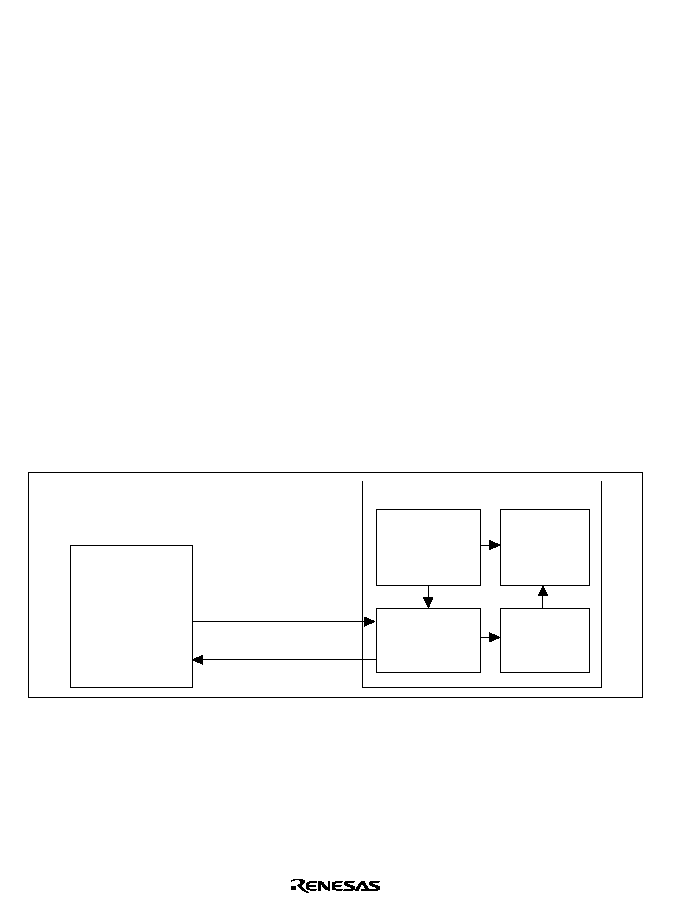
612
18.5
On-Board Programming Mode
When the pin is set in on-board programming mode and the reset start is executed, the on-board
programming state that can program/erase the on-chip flash memory is entered. On-board
programming mode has three operating modes: user programming mode, user boot mode, and
boot mode.
For details on the pin setting for entering each mode, see table 18.1. For details on the state
transition of each mode for flash memory, see figure 18.2.
18.5.1
Boot Mode
Boot mode executes programming/erasing user MAT and user boot MAT by means of the control
command and program data transmitted from the host using the on-chip SCI. The tool for
transmitting the control command and program data must be prepared in the host. The SCI
communication mode is set to asynchronous mode. When reset start is executed after this LSI's pin
is set in boot mode, the boot program in the microcomputer is initiated. After the SCI bit rate is
automatically adjusted, the communication with the host is executed by means of the control
command method.
The system configuration diagram in boot mode is shown in figure 18.6. For details on the pin
setting in boot mode, see table 18.1. The NMI and other interrupts are ignored in boot mode.
Make sure the NMI and other interrupts do not occur in the user system.
Host
RxD1
TxD1
Control command,
analysis execution
software (on-chip)
Flash
memory
On-chip RAM
On-chip SCI1
This LSI
Boot
programming
tool and program
data
Control command, program data
Reply response
Figure 18.6 System Configuration in Boot Mode
SCI Interface Setting by Host: When boot mode is initiated, this LSI measures the low period of
asynchronous SCI-communication data (H'00), which is transmitted consecutively by the host.
The SCI transmit/receive format is set to 8-bit data, 1 stop bit, and no parity. This LSI calculates
the bit rate of transmission by the host by means of the measured low period and transmits the bit
adjustment end sign (1 byte of H'00) to the host. The host must confirm that this bit adjustment
end sign (H'00) has been received normally and transmits 1 byte of H'55 to this LSI. When
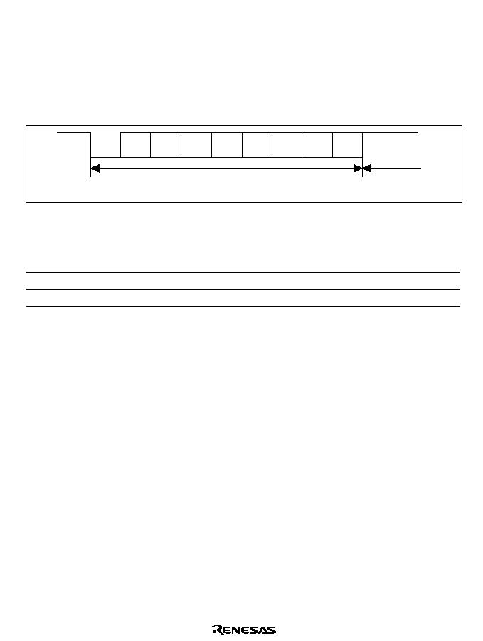
613
reception is not executed normally, boot mode is initiated again (reset) and the operation described
above must be executed. The bit rate between the host and this LSI is not matched by the bit rate
of transmission by the host and system clock frequency of this LSI. To operate the SCI normally,
the transfer bit rate of the host must be set to 9,600 bps or 19,200 bps.
The system clock frequency which can automatically adjust the transfer bit rate of the host and the
bit rate of this LSI is shown in table 18.8. Boot mode must be initiated in the range of this system
clock.
D0
D1
D2
D3
D4
D5
D6
D7
Start
bit
Stop bit
Measure low period (9 bits) (data is H'00)
High period of
at least 1 bit
Figure 18.7 Automatic Adjustment Operation of SCI Bit Rate
Table 18.8
System Clock Frequency that Can Automatically Adjust Bit Rate of This LSI
Bit rate of host
System clock frequency which can automatically adjust bit rate of this LSI
9,600 bps
10 to 25 MHz
19,200 bps
16 to 25 MHz
State Transition: The overview of the state transition after boot mode is initiated is shown in
figure 18.8. For details on boot mode, refer to section 18.10.1, Serial Communications Interface
Specification for Boot Mode.
1. Bit rate adjustment
After boot mode is initiated, the bit rate of the SCI interface is adjusted with that of the host.
2. Waiting for inquiry set command
For inquiries about user-MAT size and configuration, MAT start address, and support state, the
required information is transmitted to the host.
3. Automatic erasure of all user MAT and user boot MAT
After inquiries have finished, all user MAT and user boot MAT are automatically erased.

614
4. Waiting for programming/erasing command
� When the program preparation notice is received, the state for waiting program data is
entered. The programming start address and program data must be transmitted following the
programming command. When programming is finished, the programming start address must
be set to H'FFFFFFFF and transmitted. Then the state for waiting program data is returned to
the state of programming/erasing command wait.
� When the erasure preparation notice is received, the state for waiting erase-block data is
entered. The erase-block number must be transmitted following the erasing command. When
the erasure is finished, the erase-block number must be set to H'FF and transmitted. Then the
state for waiting erase-block data is returned to the state for waiting programming/erasing
command. The erasure must be executed when reset start is not executed and the specified
block is programmed after programming is executed in boot mode. When programming can be
executed by only one operation, all blocks are erased before the state for waiting
programming/erasing/other command is entered. The erasing operation is not required.
� There are many commands other than programming/erasing. Examples are sum check, blank
check (erasure check), and memory read of the user MAT/user boot MAT and acquisition of
current status information.
Note that memory read of the user MAT/user boot MAT can only read the program data after all
user MAT/user boot MAT has automatically been erased.
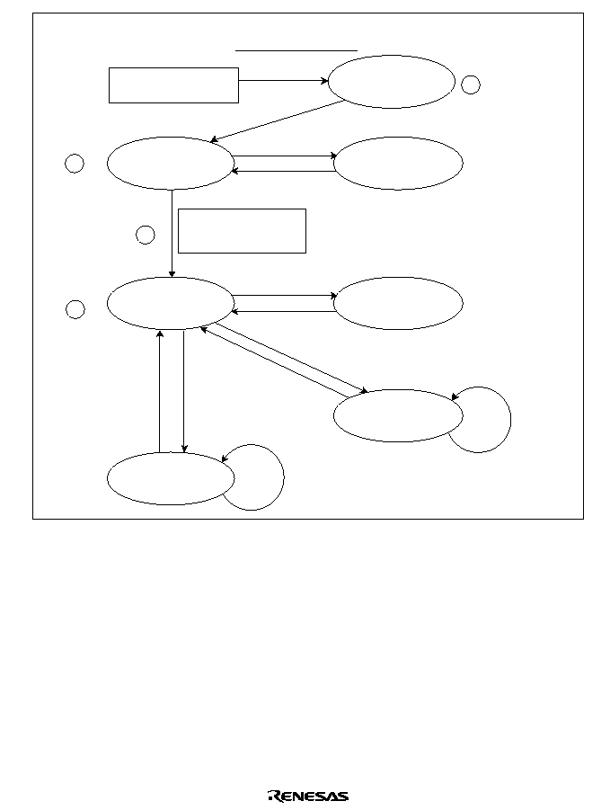
615
Wait for inquiry
setting command
Wait for
programming/erasing
command
Bit rate adjustment
Processing of
read/check command
Boot mode initiation
(reset by boot mode)
H'00 to H'00 reception
H'00 transmission
(adjustment completed)
(Bit rate adjustment)
Processing of
inquiry setting
command
All user MAT and
user boot MAT erasure
Wait for program data
Wait for erase-block
data
Read/check command
reception
Command response
(Program command reception)
(Program data transmission)
(Erasure command reception)
(Program end)
(Erase-block specification)
(Erasure end)
Inquiry command reception
H'55 reception
Inquiry command response
1
2
3
4
Figure 18.8 Overview of Boot Mode State Transition
18.5.2
User Program Mode
The user MAT can be programmed/erased in user program mode. (The user boot MAT cannot be
programmed/erased.)
Programming/erasing is executed by downloading the program in the microcomputer.
The overview flow is shown in figure 18.9.
High voltage is applied to internal flash memory during the programming/erasing processing.
Therefore, transition to reset or hardware standby must not be executed. Doing so may cause
damage or destroy flash memory. If reset is executed accidentally, reset must be released after the
reset input period, which is longer than normal 100
�
s.
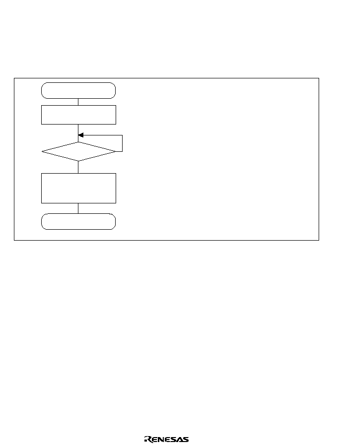
616
For information on the programming procedure refer to "Programming Procedure in User Program
Mode", and for information on the erasing procedure refer to "Erasing Procedure in User Program
Mode", below.
For the overview of a processing that repeats erasing and programming by downloading the
programming program and the erasing program in separate on-chip ROM areas using FTDAR, see
"Erasing and Programming Procedure in User Program Mode" which appears later in this section.
When programming,
program data is prepared
FWE=1 ?
Programming/erasing
procedure program is
transferred to the on-chip
RAM and executed
Yes
No
Programming/erasing
start
Programming/erasing
end
1. RAM emulation mode must be canceled
in advance. Download cannot be executed
in emulation mode.
2. When the program data is made by means
of emulation, use the FTDAR register to change
the download destination. Note that the download
area and the emulation area will overlap if FTDAR
is in its initial status (H'00) or set to H'01.
3. Inputting the FWE pin to high level sets the
FWE bit to 1.
4. Programming/erasing is executed only in
the on-chip RAM. However, if program data
is in a consecutive area and can be accessed
by the MOV.B instruction of the CPU like
SRAM/ROM, the program data can be in an
external space.
5. After programming/erasing is finished, the FWE
pin must be input to low and protected.
Figure 18.9 Programming/Erasing Overview Flow
On-chip RAM Address Map when Programming/Erasing is Executed: Parts of the procedure
program that are made by the user, like download request, programming/erasing procedure, and
judgement of the result, must be executed in the on-chip RAM. The on-chip program that is to be
downloaded is all in the on-chip RAM. Note that area in the on-chip RAM must be controlled so
that these parts do not overlap.
Figure 18.10 shows the program area to be downloaded.
617
RAM emulation area
or area that can be
used by user
RAMTOP(H'FFBF20)
DPFR
(Return value: 1 byte)
FTDAR setting
FTDAR setting+16
FTDAR setting+32
FTDAR setting+2048
<On-chip RAM>
Address
System use area
(15 bytes)
Programming/erasing entry
Initialization process entry
Initialization + programming
program or Initialization +
erasing program
Area that can be
used by user
RAMEND(H'FFFF1F)
Area to be
downloaded
(Size : 2 kbytes)
Unusable area in
programming/erasing
processing period
Figure 18.10 RAM Map when Programming/Erasing is Executed
Programming Procedure in User Program Mode: The procedures for download, initialization,
and programming are shown in figure 18.11.
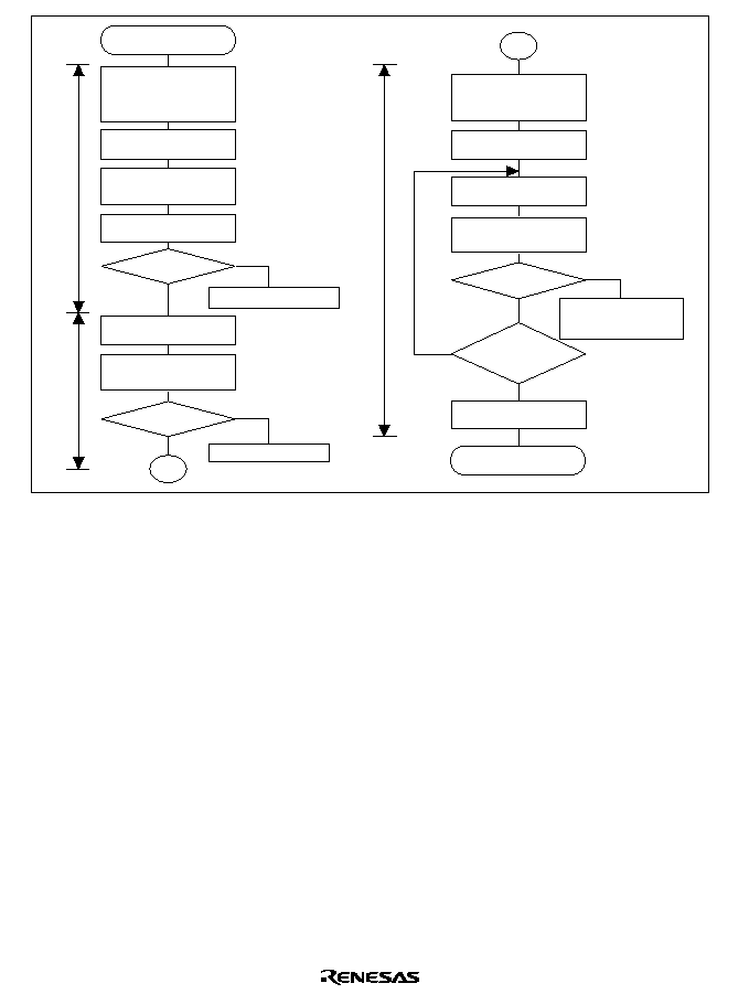
618
Select on-chip program
to be downloaded and
set download destination
by FTDAR
Set FKEY to H'A5
Set SCO to 1 and
execute download
DFPR=0?
Yes
No
Download error processing
Set the FPEFEQ and
FUBRA parameters
Initialization
JSR FTDAR setting+32
Yes
End programming
procedure program
FPFR=0?
No
Initialization error processing
Disable interrupts and bus
master operation other
than CPU
Clear FKEY to 0
Set parameter to ER0 and
ER1 (FMPAR and FMPDR)
Programming
JSR FTDAR setting+16
Yes
FPFR=0?
No
Clear FKEY and
programming
error processing
Yes
Required data
programming is
completed?
No
Set FKEY to H'5A
Clear FKEY to 0
(a)
(b)
(d)
(e)
(f)
(g)
(h)
(i)
(j)
(k)
(l)
(m)
(n)
(o)
1
1
(c)
Download
Initialization
Programming
Start programming
procedure program
Figure 18.11 Programming Procedure
The details of the programming procedure are described below. The procedure program must be
executed in an area other than the flash memory to be programmed. Especially the part where the
SCO bit in FCCS is set to 1 for downloading must be executed in the on-chip RAM.
The area that can be executed in the steps of the user procedure program (on-chip RAM, user
MAT, and external space) is shown in section 18.10.3, Procedure Program and Storable Area for
Programming Data.
The following description assumes the area to be programmed on the user MAT is erased and
program data is prepared in the consecutive area. When erasing is not executed, erasing is
executed before writing.
128-byte programming is performed in one program processing. When more than 128-byte
programming is performed, programming destination address/program data parameter is updated
in 128-byte units and programming is repeated.
When less than 128-byte programming is performed, data must total 128 bytes by adding the
invalid data. If the invalid data to be added is H'FF, the program processing period can be shorted.
(a) Select the on-chip program to be downloaded and the download destination.
When the PPVS bit of FPCS is set to 1, the programming program is selected.

619
Several programming/erasing programs cannot be selected at one time. If several programs are
set, download is not performed and a download error is returned to the source select error
detect (SS) bit in the DPFR parameter.
Specify the start address of the download destination by FTDAR.
(b) Program H'A5 in FKEY
If H'A5 is not written to FKEY for protection, 1 cannot be written to the SCO bit for download
request.
(c) 1 is written to the SCO bit of FCCS and then download is executed.
To write 1 to the SCO bit, the following conditions must be satisfied.
�
RAM emulation mode is canceled.
�
H'A5 is written to FKEY.
�
The SCO bit writing is executed in the on-chip RAM.
When the SCO bit is set to 1, download is started automatically. When the SCO bit is returned
to the user procedure program, the SCO is cleared to 0. Therefore, the SCO bit cannot be
confirmed to be 1 in the user procedure program.
The download result can be confirmed only by the return value of the DPFR parameter. Before
the SCO bit is set to 1, incorrect judgement must be prevented by setting the DPFR parameter,
that is one byte of the start address of the on-chip RAM area specified by FTDAR, to a value
other than the return value (H'FF).
When download is executed, particular interrupt processing, which is accompanied by the bank
switch as described below, is performed as an internal microcomputer processing. Four NOP
instructions are executed immediately after the instructions that set the SCO bit to 1.
�
The user-MAT space is switched to the on-chip program storage area.
�
After the selection condition of the download program and the address set in FTDAR
are checked, the transfer processing is executed starting from the on-chip RAM address
specified by FTDAR.
�
The SCO bits in FPCS, FECS, and FCCS are cleared to 0.
�
The return value is set to the DPFR parameter.
�
After the on-chip program storage area is returned to the user-MAT space, the user
procedure program is returned.
The notes on download are as follows.
In the download processing, the values are stored in general registers than CPU.
No interrupts are accepted during download processing. However, interrupt requests other than
NMI requests are held, so when processing returns to the user procedure program and
interrupts are generated. NMI requests are discarded if the FVACR register value is H'00.
However, if H'80 has been written to the FVACR register, they are held and the NMI interrupts
are generated when processing returns to the user procedure program.

620
The sources of the interrupt requests from the on-chip module and at the falling edge of the
IRQ are held during downloading. The refresh can be put in the DRAM.
When the level-detection interrupt requests are to be held, interrupts must be put until the
download is ended.
When hardware standby mode is entered during download processing, the normal download
cannot be guaranteed in the on-chip RAM. Therefore, download must be executed again.
Since a stack area of a maximum 128 bytes is used, the area must be saved before setting the
SCO bit to 1.
If flash memory is accessed by the DMAC or
BREQ during downloading, the operation cannot
be guaranteed. Therefore, access by the DMAC or
BREQ must not be executed.
(d) FKEY is cleared to H'00 for protection.
(e) The value of the DPFR parameter must be checked and the download result must be
confirmed.
A recommended procedure for confirming the download result is shown below.
�
Check the value of the DPFR parameter (one byte of start address of the download
destination specified by FTDAR). If the value is H'00, download has been performed
normally. If the value is not H'00, the source that caused download to fail can be
investigated by the description below.
�
If the value of the DPFR parameter is the same as before downloading (e.g. H'FF), the
address setting of the download destination in FTDAR may be abnormal. In this case,
confirm the setting of the TDER bit (bit 7) in FTDAR.
�
If the value of the DPFR parameter is different from before downloading, check the SS
bit (bit 2) and the FK bit (bit 1) in the DPFR parameter to ensure that the download
program selection and FKEY register setting were normal, respectively.
(f) The operating frequency and user branch destination are set to the FPEFEQ and FUBRA
parameters for initialization.
�
The current frequency of the CPU clock is set to the FPEFEQ parameter (general
register: ER0).
For the settable range of the FPEFEQ parameter, see section 21.2.1, Clock Timing.
When the frequency is set out of this range, an error is returned to the FPFR parameter
of the initialization program and initialization is not performed. For details on the
frequency setting, see the description in 18.4.3(2) (a) Flash programming/erasing
frequency parameter (FPEFEQ: general register ER0 of CPU).

621
�
The start address in the user branch destination is set to the FUBRA parameter (general
register: ER1).
Not available in the H8/3069F, 0 must be set to FUBRA.
When the user branch is executed, the branch destination is executed in a user MAT
other than the one that is to be programmed. The area of the on-chip program that is
downloaded cannot be set.
The program processing must be returned from the user branch processing by the RTS
instruction.
See the description in 18.4.3 (2) (b) Flash user branch address setting parameter
(FUBRA: general register ER1 of CPU).
(g) Initialization
When a programming program is downloaded, the initialization program is also downloaded to
the on-chip RAM. There is an entry point of the initialization program in the area from
(download start address set by FTDAR) + 32 bytes. The subroutine is called and initialization
is executed by using the following steps.
MOV.L
#DLTOP+32,ER2
; Set entry address to ER2
JSR
@ER2
; Call initialization routine
NOP
�
The general registers other than R0L are saved in the initialization program.
�
R0L is a return value of the FPFR parameter.
�
Since the stack area is used in the initialization program, a stack area of a maximum
128 bytes must be saved in RAM.
�
Interrupts can be accepted during the execution of the initialization program. The
program storage area and stack area in the on-chip RAM and register values must not
be destroyed.
(h) The return value in the initialization program, FPFR (general register R0L) is judged.
(i) All interrupts and the use of a bus master other than the CPU are prohibited.
The specified voltage is applied for the specified time when programming or erasing. If
interrupts occur or the bus mastership is moved to other than the CPU during this time, more
than the specified voltage will be applied and flash memory may be damaged. Therefore,
interrupts and movement of bus mastership to DMAC or
BREQ and DRAM refresh other than
the CPU are prohibited.
The interrupt processing prohibition is set up by setting the bit 7 (I) in the condition code
register (CCR) of the CPU to b'1. Then interrupts other than NMI are held and are not
executed.
The NMI interrupts must not occur in the user system.

622
The interrupts that are held must be processed in executed after all program processing.
When the bus mastership is moved to DMAC or
BREQ or DRAM refresh except for the CPU,
the error protection state is entered. Therefore, reservation of bus mastership by DMAC or
BREQ is prohibited.
(j) FKEY must be set to H'5A and the user MAT must be prepared for programming.
(k) The parameter which is required for programming is set.
The start address of the programming destination of the user MAT (FMPAR) is set to general
register ER1. The start address of the program data storage area (FMPDR) is set to general
register ER0.
�
Example of the FMPAR setting
FMPAR specifies the programming destination address. When an address other than
one in the user MAT area is specified, even if the programming program is executed,
programming is not executed and an error is returned to the return value parameter
FPFR. Since the unit is 128 bytes, the lower eight bits (A7 to A0) must be in the 128-
byte boundary of H'00 or H'80.
�
Example of the FMPDR setting
When the storage destination of the program data is flash memory, even if the program
execution routine is executed, programming is not executed and an error is returned to
the FPFR parameter. In this case, the program data must be transferred to the on-chip
RAM and then programming must be executed.
(l) Programming
There is an entry point of the programming program in the area from (download start address
set by FTDAR) + 16 bytes of on-chip RAM. The subroutine is called and programming is
executed by using the following steps.
MOV.L
#DLTOP+16,ER2
; Set entry address to ER2
JSR
@ER2
; Call programming routine
NOP
�
The general registers other than R0L are saved in the programming program.
�
R0 is a return value of the FPFR parameter.
�
Since the stack area is used in the programming program, a stack area of a maximum
128 bytes must be reserved in RAM
(m) The return value in the programming program, FPFR (general register R0L) is judged.
(n) Determine whether programming of the necessary data has finished.
If more than 128 bytes of data are to be programmed, specify FMPAR and FMPDR in 128-
623
byte units, and repeat steps (l) to (m). Increment the programming destination address by 128
bytes and update the programming data pointer correctly. If an address which has already been
programmed is written to again, not only will a programming error occur, but also flash
memory will be damaged.
(o) After programming finishes, clear FKEY and specify software protection.
If this LSI is restarted by a power-on reset immediately after user MAT programming has
finished, secure a reset period (period of
RES = 0) that is at least as long as normal 100
�
s.
Erasing Procedure in User Program Mode: The procedures for download, initialization, and
erasing are shown in figure 18.12.
Start erasing procedure
program
Select on-chip program
to be downloaded and set
download destination
by FTDAR
Set FKEY to H'A5
Set SCO to 1 and
execute download
DPFR = 0?
Yes
No
Download error processing
Set the FPEFEQ and
FUBRA parameters
Initialization
JSR FTDAR setting+32
Yes
End erasing
procedure program
FPFR=0 ?
No
Initialization error processing
Disable interrupts and
bus master operation
other than CPU
Clear FKEY to 0
Set FEBS parameter
Erasing
JSR FTDAR setting+16
Yes
FPFR=0 ?
No
Clear FKEY and erasing
error processing
Yes
Required block
erasing is
completed?
No
Set FKEY to H'5A
Clear FKEY to 0
(a)
(b)
(c)
(d)
(e)
(f)
1
1
Download
Initialization
Erasing
Figure 18.12 Erasing Procedure
The details of the erasing procedure are described below. The procedure program must be
executed in an area other than the user MAT to be erased. Especially the part where the SCO bit in
FCCS is set to 1 for downloading must be executed in on-chip RAM.
The area that can be executed in the steps of the user procedure program (on-chip RAM, user
MAT, and external space) is shown in section 18.10.3, Procedure Program and Storable Area for
Programming Data.

624
For the downloaded on-chip program area, refer to the RAM map for programming/erasing in
figure 18.10, RAM Map when Programming/Erasing is Executed.
A single divided block is erased by one erasing processing. For block divisions, refer to figure
18.4, Block Division of User MAT. To erase two or more blocks, update the erase block number
and perform the erasing processing for each block.
(a) Select the on-chip program to be downloaded
Set the EPVB bit in FECS to 1.
Several programming/erasing programs cannot be selected at one time. If several programs are
set, download is not performed and a download error is returned to the source select error
detect (SS) bit in the DPFR parameter.
The procedures to be carried out after setting FKEY, e.g. download and initialization, are the same
as those in the programming procedure. For details, refer to Programming Procedure in User
Program Mode in section 18.5.2.
(b) Set the FEBS parameter necessary for erasure
Set the erase block number of the user MAT in the flash erase block select parameter FEBS
(general register ER0). If a value other than an erase block number of the user MAT is set, no
block is erased even though the erasing program is executed, and an error is returned to the
return value parameter FPFR.
(c) Erasure
Similar to as in programming, there is an entry point of the erasing program in the area from
(download start address set by FTDAR) + 16 bytes of on-chip RAM. The subroutine is called
and erasing is executed by using the following steps.
MOV.L
#DLTOP+16,ER2
; Set entry address to ER2
JSR
@ER2
; Call erasing routine
NOP
�
The general registers other than R0L are saved in the erasing program.
�
R0 is a return value of the FPFR parameter.
�
Since the stack area is used in the erasing program, a stack area of a maximum 128
bytes must be reserved in RAM
(d) The return value in the erasing program, FPFR (general register R0L) is judged.
(e) Determine whether erasure of the necessary blocks has finished.
If more than one block is to be erased, update the FEBS parameter and repeat steps (b) and (c).
Blocks that have already been erased can be erased again.
(f) After erasure finishes, clear FKEY and specify software protection.
If this LSI is restarted by a power-on reset immediately after user MAT erasure has finished,
secure a reset period (period of
RES = 0) that is at least as long as normal 100
�
s.
625
(4) Erasing and Programming Procedure in User Program Mode
By changing the on-chip RAM address of the download destination in FTDAR, the erasing
program and programming program can be downloaded to separate on-chip RAM areas.
Figure 18.13 shows an example of repetitively executing RAM emulation, erasing, and
programming.
Start procedure program
Erasing program
download
Programming program
download
Emulation/Erasing/Programming
Set FTDAR to H'02
(Specify H'FFCF20 as
download destination)
Set FTDAR to H'03
(Specify H'FFBF20 as
download destination)
Download erasing program
Initialize erasing program
Initialize programming
program
Download programming
program
1
End procedure program
Enter RAM emulation mode
and tune data
in on-chip RAM
Set FMPDR to H'FFE000 to
program relevant block
(execute programming
program)
Cancel RAM emulation mode
Confirm operation
1
Erase relevant block
(execute erasing program)
End ?
Yes
No
Figure 18.13 Sample Procedure of Repeating RAM Emulation, Erasing, and Programming
(Overview)
In the above example, the erasing program and programming program are downloaded to areas
excluding the 4 kbytes (H'FFE000 to H'FFEFFF) from the start of on-chip ROM.
Download and initialization are performed only once at the beginning.
In this kind of operation, note the following:
�
Be careful not to damage on-chip RAM with overlapped settings.
In addition to the RAM emulation area, erasing program area, and programming program area,

626
areas for the user procedure programs, work area, and stack area are reserved in on-chip RAM.
Do not make settings that will overwrite data in these areas.
�
Be sure to initialize both the erasing program and programming program.
Initialization by setting the FPEFEQ and FUBRA parameters must be performed for both the
erasing program and the programming program. Initialization must be executed for both entry
addresses: (download start address for erasing program) + 32 bytes (H'FFCF40 in this
example) and (download start address for programming program) + 32 bytes (H'FFBF40 in
this example).
18.5.3
User Boot Mode
This LSI has user boot mode which is initiated with different mode pin settings than those in user
program mode or boot mode. User boot mode is a user-arbitrary boot mode, unlike boot mode that
uses the on-chip SCI.
Only the user MAT can be programmed/erased in user boot mode. Programming/erasing of the
user boot MAT is only enabled in boot mode or programmer mode.
User Boot Mode Initiation: For the mode pin settings to start up user boot mode, see table 18.1.
When the reset start is executed in user boot mode, the built-in check routine runs. The user MAT
and user boot MAT states are checked by this check routine.
While the check routine is running, NMI and all other interrupts cannot be accepted.
Next, processing starts from the execution start address of the reset vector in the user boot MAT.
At this point, H'AA is set to the flash MAT select register FMATS because the execution MAT is
the user boot MAT.
To enable NMI interrupts in a user boot MAT program, after the reset ends (
RES = 1) and TBD
�
s
passes, set NMI to 1.
User MAT Programming in User Boot Mode: For programming the user MAT in user boot
mode, additional processings made by setting FMATS are required: switching from user-boot-
MAT selection state to user-MAT selection state, and switching back to user-boot-MAT selection
state after programming completes.
Figure 18.14 shows the procedure for programming the user MAT in user boot mode.
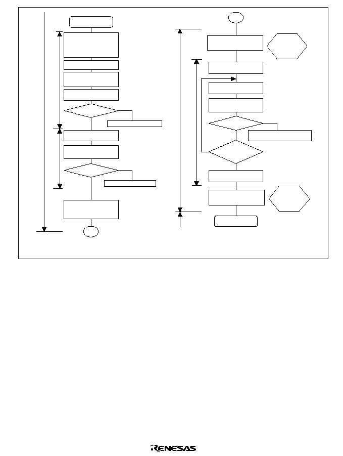
627
Select on-chip program
to be downloaded and
set download destination
by FTDAR
Set FKEY to H'A5
DPFR=0 ?
Yes
No
Download error processing
Set the FPEFEQ and
FUBRA parameters
Initialization
JSR FTDAR setting+32
Yes
End programming
procedure program
FPFR=0 ?
No
Initialization error processing
Disable interrupts
and bus master operation
other than CPU
Clear FKEY to 0
Set parameter to ER0 and
ER1 (FMPAR and FMPDR)
Programming
JSR FTDAR setting+16
Yes
FPFR=0 ?
No
Yes
Required data
programming is
completed?
No
Set FKEY to H'5A
Clear FKEY to 0
1
1
Download
Initialization
Programming
MAT
switchover
MAT
switchover
Set FMATS to value other than
H'AA to select user MAT
Set SCO to 1 and
execute download
Clear FKEY and programming
error processing
*
Set FMATS to H'AA to
select user boot MAT
User-boot-MAT selection state
User-MAT selection state
User-boot-MAT
selection state
Note:
*
The MAT must be switched by FMATS
to perform the programming error
processing in the user boot MAT.
Start programming
procedure program
Figure 18.14 Procedure for Programming User MAT in User Boot Mode
The difference between the programming procedures in user program mode and user boot mode is
whether the MAT is switched or not as shown in figure 18.14.
In user boot mode, the user boot MAT can be seen in the flash memory space with the user MAT
hidden in the background. The user MAT and user boot MAT are switched only while the user
MAT is being programmed. Because the user boot MAT is hidden while the user MAT is being
programmed, the procedure program must be located in an area other than flash memory. After
programming finishes, switch the MATs again to return to the first state.
MAT switchover is enabled by writing a specific value to FMATS. However note that while the
MATs are being switched, the LSI is in an unstable state, e.g. access to a MAT is not allowed until
MAT switching is completely finished, and if an interrupt occurs, from which MAT the interrupt
vector is read from is undetermined. Perform MAT switching in accordance with the description
in section 18.8, Switching between User MAT and User Boot MAT.
Except for MAT switching, the programming procedure is the same as that in user program mode.
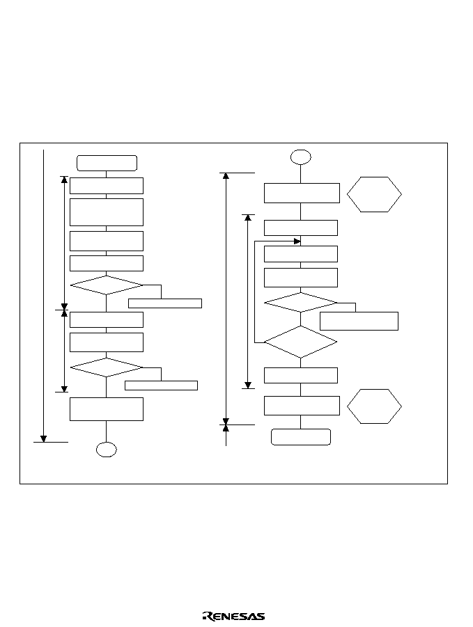
628
The area that can be executed in the steps of the user procedure program (on-chip RAM, user
MAT, and external space) is shown in section 18.10.3, Procedure Program and Storable Area for
Programming Data.
User MAT Erasing in User Boot Mode: For erasing the user MAT in user boot mode, additional
processings made by setting FMATS are required: switching from user-boot-MAT selection state
to user-MAT selection state, and switching back to user-boot-MAT selection state after erasing
completes.
Figure 18.15 shows the procedure for erasing the user MAT in user boot mode.
Start erasing
procedure program
Select on-chip program
to be downloaded
Set FKEY to H'A5 and
set download destination
by FTDAR
DPFR=0 ?
Yes
No
Download error processing
Set the FPEFEQ and
FUBRA parameters
Initialization
JSR FTDAR setting+32
Yes
End erasing
procedure program
FPFR=0 ?
No
Initialization error processing
Disable interrupts
and bus master operation
other than CPU
Clear FKEY to 0
Set FEBS parameter
Programming
JSR FTDAR setting+16
Yes
FPFR=0 ?
No
Clear FKEY and erasing
error processing
Yes
Required
block erasing is
completed?
No
Set FKEY to H'5A
Clear FKEY to 0
1
1
Download
Initialization
Erasing
Set FMATS to value other
than H'AA to select user MAT
Set SCO to 1 and
execute download
Set FMATS to H'AA to
select user boot MAT
User-boot-MAT selection state
User-MAT selection state
User-boot-MAT
selection state
Note: The MAT must be switched by FMATS to perform the
erasing error processing in the user boot MAT.
MAT
switchover
MAT
switchover
Figure 18.15 Procedure for Erasing User MAT in User Boot Mode
The difference between the erasing procedures in user program mode and user boot mode depends
on whether the MAT is switched or not as shown in figure 18.15.
MAT switching is enabled by writing a specific value to FMATS. However note that while the
MATs are being switched, the LSI is in an unstable state, e.g. access to a MAT is not allowed until
MAT switching is completed finished, and if an interrupt occurs, from which MAT the interrupt

629
vector is read from is undetermined. Perform MAT switching in accordance with the description
in section 18.8, Switching between User MAT and User Boot MAT.
Except for MAT switching, the erasing procedure is the same as that in user program mode.
The area that can be executed in the steps of the user procedure program (on-chip RAM, user
MAT, and external space) is shown in section 18.10.3, Procedure Program and Storable Area for
Programming Data.

630
18.6
Protection
There are two kinds of flash memory program/erase protection: hardware and software protection.
18.6.1
Hardware Protection
Programming and erasing of flash memory is forcibly disabled or suspended by hardware
protection. In this state, the downloading of an on-chip program and initialization of the flash
memory are possible. However, an activated program for programming or erasure cannot program
or erase locations in a user MAT, and the error in programming/erasing is reported in the
parameter FPFR.

631
Table 18.9
Hardware Protection
Function to be Protected
Item
Description
Download
Program/Erase
FWE-pin protection
�
The input of a low-level signal on the
FWE pin clears the FWE bit of FCCS
and the device enters a
program/erase-protected state.
--
Reset/standby
protection
�
A power-on reset (including a power-
on reset by the WDT) and entry to
standby mode reinitialize the
program/erase interface register and
the device enters a program/erase-
protected state.
�
Resetting by means of the
RES
pin
after power is initially supplied will
not make the device enter the reset
state unless the
RES
pin is held low
until oscillation has stabilized. In the
case of a reset during operation,
hold the
RES
pin low for the RES
pulse width that is specified in the
section on AC characteristics
section. If the device is reset during
programming or erasure, data values
in the flash memory are not
guaranteed. In this case, after
keeping the
RES
pin low for at least
100
�
s, execute erasure and then
execute programming again.
18.6.2
Software Protection
Software protection is set up in any of three ways: by disabling the downloading of on-chip
programs for programming and erasing, by means of a key code, and by the RAM-emulation
register.

632
Table 18.10 Software Protection
Function to be Protected
Item
Description
Download
Program/Erase
Protection by the
SCO bit
�
Clearing the SCO bit in the FCCS
register makes the device enter a
program/erase-protected state, and
this disables the downloading of the
programming/erasing programs.
Protection by the
FKEY register
�
Downloading and
programming/erasing are disabled
unless the required key code is
written in the FKEY register.
Different key codes are used for
downloading and for
programming/erasing.
Emulation
protection
�
Setting the RAMS bit in the RAM
emulation register (RAMER) makes
the device enter a program/erase-
protected state.
18.6.3
Error Protection
Error protection is a mechanism for aborting programming or erasure when an error occurs, in the
form of the microcomputer entering runaway during programming/erasing of the flash memory or
operations that are not according to the established procedures for programming/erasing. Aborting
programming or erasure in such cases prevents damage to the flash memory due to excessive
programming or erasing.
If the microcomputer malfunctions during programming/erasing of the flash memory, the FLER
bit in the FCCS register is set to 1 and the device enters the error-protection state, and this aborts
the programming or erasure.
The FLER bit is set in the following conditions:
(1) When an interrupt, such as NMI, has occurred during programming/erasing
(2) When the relevant block area of flash memory is read during programming/erasing (including
a vector read or an instruction fetch)
(3) When a SLEEP instruction (including software standby mode) is executed during
programming/erasing
(4) When a bus master other than the CPU, such as DMAC or
BREQ, has obtained the bus right
during programming/erasing
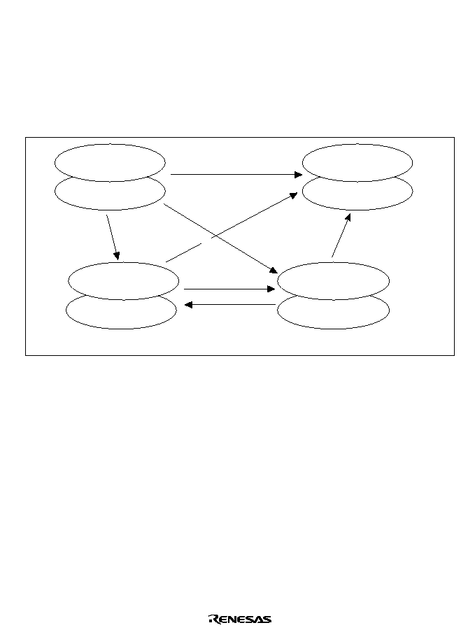
633
Error protection is cancelled only by a power-on reset or by hardware-standby mode. Note that the
reset should only be released after providing a reset input over a period longer than the normal 100
�
s period. Since high voltages are applied during programming/erasing of the flash memory, some
voltage may remain after the error-protection state has been entered. For this reason, it is
necessary to reduce the risk of damage to the flash memory by extending the reset period so that
the charge is released.
The state-transition diagram in figure 18.16 shows transitions to and from the error-protection
state.
Reset or standby
(Hardware protection)
Program mode
Erase mode
Error protection mode
Error-protection mode
(Software standby)
Read disabled
Programming/erasing
enabled FLER=0
Read disabled
Programming/erasing disabled
FLER=0
Read enabled
Programming/erasing disabled
FLER=1
Read disabled
programming/erasing disabled
FLER=1
RES
= 0 or
STBY
= 0
Error occurrence
Error occurrence
(Software standby)
RES
=0 or
STBY
=0
Software-standby mode
Cancel
software-standby mode
RES
=0 or
STBY
=0
Program/erase interface
register is in its initial state.
Program/erase interface
register is in its initial state.
Figure 18.16 Transitions to and from the Error-Protection State
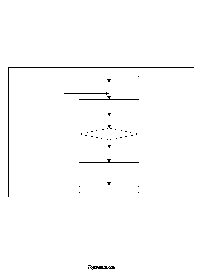
634
18.7
Flash Memory Emulation in RAM
To provide real-time emulation in RAM of data that is to be written to the flash memory, a part of
the RAM can be overlaid on an area of flash memory (user MAT) that has been specified by the
RAM control register (RAMCR). After the RAMCR setting is made, the RAM is accessible in
both the user MAT area and as the RAM area that has been overlaid on the user MAT area. Such
emulation is possible in both user mode and user-program mode.
Figures 18.17 and 18.18 show an example of the emulation of realtime programming of the user
MAT area.
Start of emulation program
Set RAMCR
Write the data for tuning to
the overlaid RAM area
Execute application program
Tuning OK?
Cancel RAMCR setting
Program the user MAT
with the emulated block
End of emulation program
Yes
No
Figure 18.17 Emulation of Flash Memory in RAM
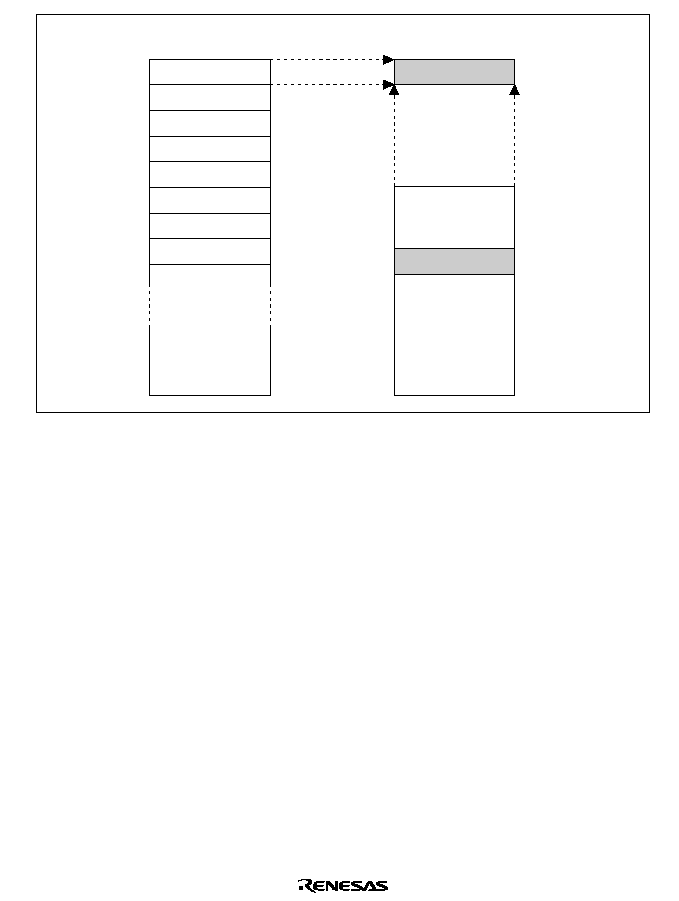
635
EB0
H'00000
EB1
H'01000
EB2
H'02000
EB3
H'03000
EB4
H'04000
EB5
H'05000
EB6
H'06000
EB7
H'07000
H'08000
H'7FFFF
Flash memory
(user MAT)
EB8 to EB15
H'FFE000
H'FFBF20
H'FFEFFF
H'FFFF1F
On-chip RAM
This area is accessible as both a RAM
area and as a flash memory area.
Figure 18.18 Example of a RAM-Overlap Operation
Figure 18.18 shows an example of an overlap on block area EB0 of the flash memory.
Emulation is possible for a single area selected from among the eight areas, from EB0 to EB7, of
user MAT bank 0. The area is selected by the setting of the RAM2 to RAM0 bits in the RAMCR
register.
(1) To overlap a part of the RAM on area EB0, to allow realtime programming of the data for this
area, set the RAMCR register's RAMS bit to 1, and each of the RAM2 to RAM0 bits to 0.
(2) Realtime programming is carried out using the overlaid area of RAM.
In programming or erasing the user MAT, it is necessary to run a program that implements a series
of procedural steps, including the downloading of a on-chip program. In this process, set the
download area with FTDAR so that the overlaid RAM area and the area where the on-chip
program is to be downloaded do not overlap. The initial setting (H'00) of FTDAR or a setting of
H'01 causes part of the tuned data area to overlap with part of the download area. When using the
initial setting of FTDAR, the data that is to be programmed must be saved beforehand in an area
that is not used by the system.
Figure 18.19 shows an example of programming of the data, after emulation has been completed,
to the EB0 area in the user MAT.
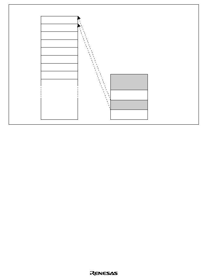
636
EB0
H'00000
EB1
H'01000
EB2
H'02000
EB3
H'03000
EB4
H'04000
EB5
H'05000
EB6
H'06000
EB7
H'07000
H'08000
H'7FFFF
Flash memory
(user MAT)
EB8 to EB15
H'FFCF20
H'FFD720
H'FFE000
H'FFEFFF
H'FFFF1F
On-chip RAM
Download area
Area for the
programming-procedure
program
Copy of the tuned data
(1) Cancel the emulation mode.
(2) Transfer the user-created program/
erase-procedure program.
(3) Download the on-chip programming/erasing
programs, avoiding the tuning <illegible>
data area set in FTDAR.
(4) Execute programming after erasing,
as necessary.
Figure 18.19 Programming of the Data After Tuning
(1) After the data to be programmed has fixed values, clear the RAMS bit to 0 to cancel the
overlap of RAM.
(2) Transfer the user programming/erasing procedure program to RAM.
(3) Run the programming/erasing procedure program in RAM and download the on-chip
programming/erasing program.
Specify the download start address with FTDAR so that the tuned data area does not overlap
with the download area.
(4) When the EB0 area of the user MAT has not been erased, the programming program will be
downloaded after erasure. Set the parameters FMPAR and FMPDR so that the tuned data is
designated, and execute programming.
Note: Setting the RAMS bit to 1 puts all the blocks in the flash MAT into a program/erase-
protected state regardless of the values of the RAM2 to RAM0 bits (emulation protection).
In this state, downloading of the on-chip programs is also disabled, so clear the RAMS bit
before actual programming or erasure.
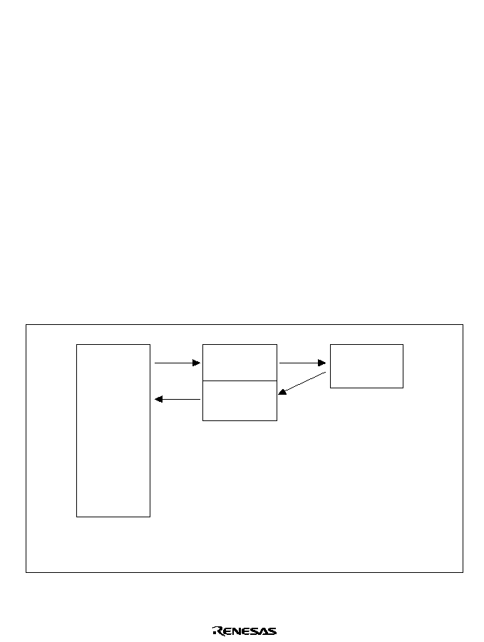
637
18.8
Switching between User MAT and User Boot MAT
It is possible to alternate between the user MAT and user boot MAT. However, the following
procedure is required because these MATs are allocated to address 0.
(Switching to the user boot MAT disables programming and erasing. Programming of the user
boot MAT should take place in boot mode or PROM mode.)
(1) MAT switching by the FMATS register should always be executed from the on-chip RAM.
(2) To ensure that the MAT that has been switched to is accessible, execute 4 NOP instructions in
the on-chip RAM immediately before or after writing to the FMATS register of the on-chip
RAM (this prevents access to the flash memory during MAT switching).
(3) If an interrupt has occurred during switching, there is no guarantee of which memory MAT is
being accessed. Always mask the maskable interrupts before switching between MATs. In
addition, configure the system so that NMI interrupts do not occur during MAT switching.
(4) After the MATs have been switched, take care because the interrupt vector table will also have
been switched. If interrupt processing is to be the same before and after MAT switching,
transfer the interrupt-processing routines to the on-chip RAM, and use the settings of the
FVACR and FVADR registers to place the interrupt-vector table in the on-chip RAM .
(5) Memory sizes of the user MAT and user boot MAT are different. When accessing the user
boot MAT, do not access addresses above the top of its 8-kbyte memory space. If access goes
beyond the 8-kbyte space, the values read are undefined.
<User MAT>
<On-chip RAM>
<User boot MAT>
Procedure for
switching to the
user boot MAT
Procedure for
switching to
the user MAT
Procedure for switching to the user boot MAT
(1) Mask interrupts
(2) Write H'AA to the FMATS register.
(3) Execute 4 NOP instructions before
accessing the user boot MAT.
Procedure for switching to the user MAT
(1) Mask interrupts
(2) Write a value other than H'AA to the FMATS register.
(3) Execute 4 NOP instructions before or after accessing
the user MAT.
Figure 18.20 Switching between the User MAT and User Boot MAT

638
18.8.1
Usage Notes
1. Download time of on-chip program
The programming program that includes the initialization routine and the erasing program that
includes the initialization routine are each 2 kbytes or less. Accordingly, when the CPU clock
frequency is 25 MHz, the download for each program takes approximately 164
�
s at maximum.
2. Write to flash-memory related registers by DMAC
While an instruction in on-chip RAM is being executed, the DMAC can write to the SCO bit in
FCCS that is used for a download request or FMATS that is used for MAT switching. Make sure
that these registers are not accidentally written to, otherwise an on-chip program may be
downloaded and damage RAM or a MAT switchover may occur and the CPU get out of control.
Do not use DMAC to program FLASH related registers.
3. Compatibility with programming/erasing program of conventional F-ZTAT H8 microcomputer
A programming/erasing program for flash memory used in the conventional F-ZTAT H8
microcomputer which does not support download of the on-chip program by a SCO transfer
request cannot run in this LSI.
Be sure to download the on-chip program to execute programming/erasing of flash memory in this
LSI.
4. Monitoring runaway by WDT
Unlike the conventional F-ZTAT H8 microcomputer, no countermeasures are available for a
runaway by WDT during programming/erasing by the downloaded on-chip program.
Prepare countermeasures (e.g. use of the user branch routine and periodic timer interrupts) for
WDT while taking the programming/erasing time into consideration as required.

639
18.9
PROM Mode
Along with its on-board programming mode, this LSI also has a PROM mode as a further mode
for the writing and erasing of programs and data. In the PROM mode, a general-purpose PROM
programmer can freely be used to write programs to the on-chip ROM. Program/erase is possible
on the user MAT and user boot MAT. The PROM programmer must support Hitachi
microcomputers with 512-kbyte flash memory units as a device type.
A status-polling system is adopted for operation in automatic program, automatic erase, and
status-read modes. In the status-read mode, details of the system's internal signals are output after
execution of automatic programming or automatic erasure. In the PROM mode, provide a 12-MHz
input-clock signal.
Table 18.11 PROM Mode Pin
Pins
Setting
Mode pin: P82, P81, P80
1, 0, 0
18.9.1
Pin Arrangement of the Socket Adapter
Attach the socket adapter to the LSI in the way shown in figure 18.22. This allows conversion to
40 pins. Figure 18.21 shows the memory mapping of the on-chip ROM, and figure 18.22 shows
the arrangement of the socket adapter's pins.
H'000000
H'07FFFF
Address in
MCU mode
Address in
MCU mode
Address in
PROM mode
Address in
PROM mode
H'00000
H'7FFFF
H'000000
H'001FFF
H'00000
H'01FFF
On-chip ROM space
(user boot MAT) 8kB
On-chip ROM space
(user MAT)
512kB
Figure 18.21 Mapping of On-Chip Flash Memory
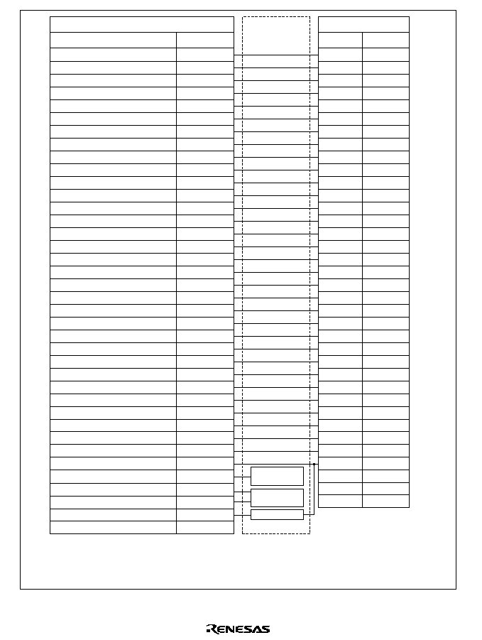
640
H8/3069F
Socket Adapter
(40-Pin Conversion)
Pin No.
Pin Name
36
37
38
39
40
41
42
43
45
64
47
48
49
50
51
58
69
70
55
27
28
29
30
31
32
33
34
52
46
90
10
A0
A1
A2
A3
A4
A5
A6
A7
A8
A9
A10
A11
A12
A13
A14
A15
A16
A17
A18
D0
D1
D2
D3
D4
D5
D6
D7
CE
OE
WE
FWE
HN27C4096HG (40 pins)
Pin No.
Pin Name
21
22
23
24
25
26
27
28
29
31
32
33
34
35
36
37
38
39
10
19
18
17
16
15
14
13
12
2
20
3
4
1,40
11,30
5,6,7
8
9
A0
A1
A2
A3
A4
A5
A6
A7
A8
A9
A10
A11
A12
A13
A14
A15
A16
A17
A18
I/O0
I/O1
I/O2
I/O3
I/O4
I/O5
I/O6
I/O7
CE
OE
WE
FWE
V
CC
V
SS
NC
A20
A19
63
67
66
1
Other
RES
XTAL
EXTAL
V
CL
N.C.(OPEN)
76,77,62,71,89,35,68
73,74,75,87,88,86,11,22,44,57,65,92,14
V
CC
V
SS
Power-on
reset circuit
Capacitor
Oscillator
circuit
Legend
FWE
: Flash-write enable
I/O7 to 0 : Data I/O
A18 to 0 : Address input
CE
: Chip enable
OE
: Output enable
WE
: Write enable
Figure 18.22 Pin Arrangement of the Socket Adapter

641
18.9.2
PROM Mode Operation
Table 18.12 shows the settings for the operating modes of PROM mode, and table 18.13 lists the
commands used in PROM mode. The following sections provide detailed information on each
mode.
�
Memory-read mode: This mode supports reading, in units of bytes, from the user MAT or user
boot MAT.
�
Auto-program mode: This mode supports the simultaneous programming of the user MAT and
user boot MAT in 128-byte units. Status polling is used to confirm the end of automatic
programming.
�
Auto-erase mode: This mode only supports the automatic erasing of the entire user MAT or
user boot MAT. Status polling is used to confirm the end of automatic erasing.
�
Status-read mode: Status polling is used with automatic programming and automatic erasure.
Normal completion can be detected by reading the signal on the I/O6 pin. In status-read mode,
error information is output when an error has occurred.
Table 18.12 Settings for Each Operating Mode of PROM Mode
Pin Name
Mode
FWE
CE
OE
WE
I/O7 to 0
A18 to 0
Read
H or L
L
L
H
Data output
Ain
Output disable
H or L
L
H
H
Hi-Z
X
Command write
H or L
L
H
L
Data input
*
Ain
Chip disable
H or L
H
X
X
Hi-Z
X
Notes: 1. The chip-disable mode is not a standby state; internally, it is an operational state.
2. To write commands when making a transition to the auto-program or auto-erase mode,
input a high-level signal on the FWE pin.
*
Ain indicates that there is also an address input in auto-program mode.

642
Table 18.13 Commands in PROM Mode
Number
Memory
MAT to
1
st
Cycle
2
nd
Cycle
Command
of
Cycles
be
Accessed
Mode
Address
Data
Mode
Address
Data
Memory-read
mode
1+n
User MAT
write
X
H'00
read
RA
Dout
User boot
MAT
write
X
H'05
Auto-program
mode
129
User MAT
write
X
H'40
write
WA
Din
User boot
MAT
write
X
H'45
Auto-erase
mode
2
User MAT
write
X
H'20
write
X
H'20
User boot
MAT
write
X
H'25
H'25
Status-read
mode
2
Common
to both
MATs
write
X
H'71
write
X
H'71
Notes: 1. In auto-program mode, 129 cycles are required in command writing because of the
simultaneous 128-byte write.
2. In memory read mode, the number of cycles varies with the number of address writing
cycles (n).
18.9.3
Memory-Read Mode
(1) On completion of an automatic program, automatic erase, or status read, the LSI enters a
command waiting state. So, to read the contents of memory after these operations, issue the
command to change the mode to the memory-read mode before reading from the memory.
(2) In memory-read mode, the writing of commands is possible in the same way as in the
command-write state.
(3) After entering memory-read mode, continuous reading is possible.
(4) After power has first been supplied, the LSI enters the memory-read mode. For the AC
characteristics in memory read mode, see section 18.10.2, AC Characteristics and Timing in
Writer Mode.
18.9.4
Auto-Program Mode
(1) In auto-program mode, programming is in 128-byte units. That is, 128 bytes of data are
transferred in succession.

643
(2) Even in the programming of less than 128 bytes, 128 bytes of data must be transferred. H'FF
should be written to those addresses that are unnecessarily written to.
(3) Set the low seven bits of the address to be transferred to low level. Inputting an invalid address
will result in a programming error, although processing will proceed to the memory-
programming operation.
(4) The memory address is transferred in the 2
nd
cycle. Do not transfer addresses in the 3
rd
or later
cycles.
(5) Do not issue commands while programming is in progress.
(6) When programming, execute automatic programming once for each 128-byte block of
addresses. Programming the block at an address where programming has already been
performed is not possible.
(7) To confirm the end of automatic programming, check the signal on the I/O6 pin. Confirmation
in the status-read mode is also possible (status polling of the I/O7 pin is used to check the end
status of automatic programming).
(8) Status-polling information on the I/O6 and I/O7 pins is retained until the next command is
written. As long as no command is written, the information is made readable by setting
CE and
OE for enabling.
For the AC characteristics in auto-program mode, see section 18.10.2, AC Characteristics and
Timing in Writer Mode.
18.9.5
Auto-Erase Mode
(1) Auto-erase mode only supports erasing of the entire memory.
(2) Do not perform command writing during auto erasing is in progress.
(3) To confirm the end of automatic erasing, check the signal on the I/O6 pin. Confirmation in the
status-read mode is also possible (status polling of the I/O7 pin is used to check the end status
of automatic erasure).
(4) Status polling information on the I/O6 and I/O7 pins is retained until the next command
writing. As long as no command is written, the information is made readable by setting
CE and
OE for enabling.
For the AC characteristics in auto-erase mode, see section 18.10.2, AC Characteristics and Timing
in Writer Mode.

644
18.9.6
Status-Read Mode
(1) Status-read mode is used to determine the type of an abnormal termination. Use this mode
when automatic programming or automatic erasure ends abnormally.
(2) The return code is retained until writing of a command that selects a mode other than status-
read mode.
Table 18.14 lists the return codes of status-read mode.
For the AC characteristics in status-read mode, see section 18.10.2, AC Characteristics and
Timing in Writer Mode.
Table 18.14 Return Codes of Status-Read Mode
Pin Name I/O7
I/O6
I/O5
I/O4
I/O3
I/O2
I/O1
I/O0
Attribute
Normal end
indicator
Command
error
Program-
ming error
Erase error --
--
Programming
or erase
count
exceeded
Invalid
address
error
Initial value 0
0
0
0
0
0
0
0
Indication
Normal
end: 0
Abnormal
end: 1
Command
error: 1
Otherwise: 0
Program-
ming error: 1
Otherwise: 0
Erase
error:1
Otherwise: 0
--
--
Count
exceeded: 1
Otherwise: 0
Invalid
address
error: 1
Otherwise: 0
Note: I/O2 and I/O3 are undefined pins.
18.9.7
Status Polling
(1) The I/O7 status-polling output is a flag that indicates the operating status in auto-program or
auto-erase mode.
(2) The I/O6 status-polling output is a flag that indicates normal/abnormal end of auto-program or
auto-erase mode.
Table 18.15 Truth Table of Status-Polling Output
Pin Name
In Progress
Abnormal End
--
Normal End
I/O7
0
1
0
1
I/O6
0
0
1
1
I/O0 to 5
0
0
0
0

645
18.9.8
Time Taken in Transition to PROM Mode
Until oscillation has stabilized and while PROM mode is being set up, the LSI is unable to accept
commands. After the PROM-mode setup time has elapsed, the LSI enters memory-read mode. See
section 18.10.2, AC Characteristics and Timing in Writer Mode.
18.9.9
Notes on Using PROM Mode
(1) When programming addresses which have previously been programmed, apply auto-erasing
before auto-programming (figure 18.24).
(2) When using PROM mode to program a chip that has been programmed/erased in an on-board
programming mode, auto-erasing before auto-programming is recommended.
(3) Do not take the chip out of the PROM programmer or reset the chip during programming or
erasure. Flash memory is susceptible to permanent damage since a high voltage is being
applied during the programming/erasing. When the reset signal is accidentally input to the
chip, the period in the reset state until the reset signal is released should be longer than the
normal 100
�
s.
(4) The flash memory is initially in the erased state when the device is shipped by Hitachi. For
other chips for which the history of erasure is unknown, auto-erasing as a check and
supplement for the initialization (erase) level is recommended.
(5) This LSI does not support modes such as the product identification mode of general purpose
EPROM. Therefore, the device name is not automatically set in the PROM programmer.
(6) For further information on the PROM programmer and its software version, please refer to the
instruction manual for the socket adapter.

646
18.10
Further Information
18.10.1
Serial Communication Interface Specification for Boot Mode
Initiating boot mode enables the boot program to communicate with the host by using the internal
SCI. The serial communication interface specification is shown below.
�
Status
The boot program has three states.
(1) Bit-Rate-Adjustment State
In this state, the boot program adjusts the bit rate to communicate with the host. Initiating boot
mode enables starting of the boot program and entry to the bit-rate-adjustment state. The
program receives the command from the host to adjust the bit rate. After adjusting the bit rate,
the program enters the inquiry/selection state.
(2) Inquiry/Selection State
In this state, the boot program responds to inquiry commands from the host. The device name,
clock mode, and bit rate are selected. After selection of these settings, the program is made to
enter the programming/erasing state by the command for a transition to the
programming/erasing state. The program transfers the libraries required for erasure to the
RAM and erases the user MATs and user boot MATs before the transition.
(3) Programming/erasing state
Programming and erasure by the boot program take place in this state. The boot program is
made to transfer the programming/erasing programs to the RAM by commands from the host.
Sum checks and blank checks are executed by sending these commands from the host.
These boot program states are shown in figure 18.23.
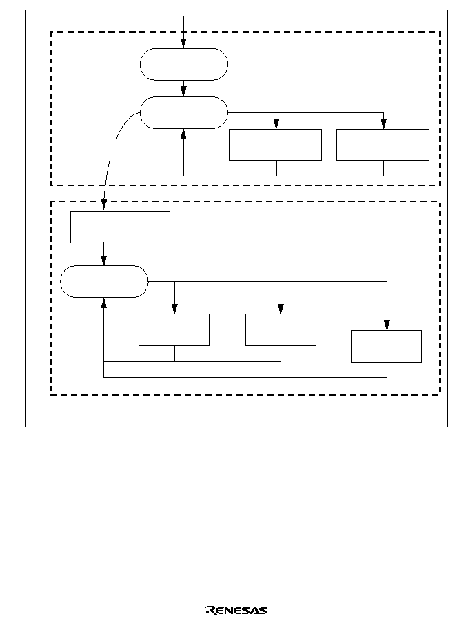
647
Transition to
Programming/erasing
Inquiry/Selection
wait
Programming/erasing
selection wait
Checking
Inquiry
Selection
Erasing
Programming
Reset
Bit-Rate-Adjustment
State
Operations for Erasing
User MATs and User
Boot MATs
Operations for
Inquiry
Operations for
Selection
Operations for
Programming
Operations for
Checking
Operations for
Erasing
Figure 18.23 Boot Program States
�
Bit-Rate-Adjustment state
The bit rate is calculated by measuring the period of transfer of a low-level byte (H'00) from the
host. The bit rate can be changed by the command for a new bit rate selection. After the bit rate
has been adjusted, the boot program enters the inquiry and selection state. The bit-rate-adjustment
sequence is shown in figure 18.24.
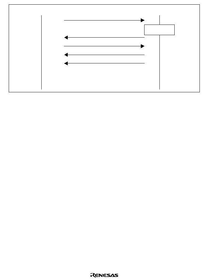
648
Host
Boot Program
H'00 (30 times maximum)
H'E6 (Response to Boot)
Measuring the
1-Bit Length
H'00 (Completion of Adjustment)
H'55
H'FF (Error)
Figure 18.24 Bit-Rate-Adjustment Sequence
�
Communications Protocol
After adjustment of the bit rate, the protocol for communications between the host and the boot
program is as shown below.
(1) One-byte commands and one-byte responses
These commands and responses are comprised of a single byte. These are consists of the
inquiries and the ACK for successful completion.
(2) n-byte commands or n-byte responses
These commands and responses are comprised of n bytes of data. These are selections and
responses to inquiries.
The amount of programming data is not included under this heading because it is determined in
another command.
(3) Error response
The error response is a response to inquiries. It consists of an error response and an error code
and comes two bytes.
(4) Programming of 128 bytes
The size is not specified in commands. The size of n is indicated in response to the
programming unit inquiry.
(5) Memory read response
This response consists of four bytes of data.
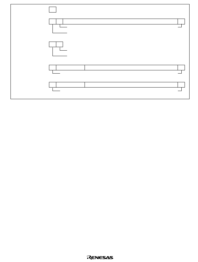
649
Command or Response
Size
Data
Checksum
Error Response
Error Code
Command or Response
Error Response
n-Byte Command or
n-Byte Response
One-Byte Command
or One-Byte Response
Address
Command
Data (n bytes)
Checksum
128-Byte Programming
Size
Response
Data
Checksum
Memory Read
Response
Figure 18.25 Communication Protocol Format
Command (1 byte) : Commands including inquiries, selection, programming, erasing, and
checking
Response (1 byte) : Response to an inquiry
Size (1 byte) : The amount of data for transmission excluding the command, amount of
data, and checksum
Checksum (1 byte) : The checksum is calculated so that the total of all values from the
command byte to the SUM byte becomes H'00.
Data (n bytes) : Detailed data of a command or response
Error Response (1 byte) : Error response to a command
Error Code (1 byte) : Type of the error
Address (4 bytes) : Address for programming
Data (n bytes) : Data to be programmed (the size is indicated in the response to the
programming unit inquiry.)
Size (4 bytes) : Four-byte response to a memory read

650
�
Inquiry and Selection States
The boot program returns information from the flash memory in response to the host's inquiry
commands and sets the device code, clock mode, and bit rate in response to the host's selection
command.
Inquiry and selection commands are listed below.
Table 18.16 Inquiry and Selection Commands
Command
Command Name
Description
H'20
Supported Device Inquiry
Inquiry regarding device codes and
product names of F-ZTAT
H'10
Device Selection
Selection of device code
H'21
Clock Mode Inquiry
Inquiry regarding numbers of clock
modes and values of each mode
H'11
Clock Mode Selection
Indication of the selected clock mode
H'22
Multiplication Ratio Inquiry
Inquiry regarding the number of
frequency-multiplied clock types, the
number of multiplication ratios, and the
values of each multiple
H'23
Operating Clock Frequency Inquiry
Inquiry regarding the maximum and
minimum values of the main clock and
peripheral clocks
H'24
User Boot MAT Information Inquiry
Inquiry regarding the number of user
boot MATs and the start and last
addresses of each MAT
H'25
User MAT Information Inquiry
Inquiry regarding the a number of user
MATs and the start and last addresses
of each MAT
H'26
Block for Erasing Information Inquiry
Inquiry regarding the number of blocks
and the start and last addresses of each
block
H'27
Programming Unit Inquiry
Inquiry regarding the unit of
programming data
H'3F
New Bit Rate Selection
Selection of new bit rate
H'40
Transition to Programming/erasing State
Erasing of user MAT and user boot
MAT, and entry to programming/erasing
state
H'4F
Boot Program Status Inquiry
Inquiry into the operated status of the
boot program
The selection commands, which are device selection (H'10), clock mode selection (H'11), and new
bit rate selection (H'3F), should be sent from the host in that order. These commands will

651
certainly be needed. When two or more selection commands are sent at once, the last command
will be valid.
All of these commands, except for the boot program status inquiry command (H'4F), will be valid
until the boot program receives the programming/erasing transition (H'40). The host can choose
the needed commands out of the commands and inquiries listed above. The boot program status
inquiry command (H'4F) is valid after the boot program has received the programming/erasing
transition command (H'40).
(1) Supported device inquiry
The boot program will return the device codes of supported devices and the product code of the
F-ZTAT in response to the supported device inquiry.
Command
H'20
Command, H'20, (1 byte) : Inquiry regarding supported devices
Response
H'30
Size
A number of
devices
A number of
characters
Device code
Product name
���
SUM
Response, H'30, (1 byte) : Response to the supported device inquiry
Size (1 byte) : Number of bytes to be transmitted, excluding the command, amount of data,
and checksum, that is, the amount of data contributes by the product names, the number of
devices, characters, and device codes
A number of devices (1 byte) : The number of device types supported by the boot program
A number of characters (1 byte) : The number of characters in the device codes and boot
program's name
Device code (4 bytes) : Code of the supporting product
Product name (n bytes) : Type name of the boot program in ASCII-coded characters
SUM (1 byte) : Checksum
The checksum is calculated so that the total number of all values from the command byte
to the SUM byte becomes H'00.
(2) Device Selection
The boot program will set the supported device to the specified device code. The program will
return the selected device code in response to the inquiry after this setting has been made.
Command
H'10
Size
Device code
SUM
Command, H'10, (1 byte) : Device selection

652
Size (1 byte) : Amount of device-code data
This is fixed to 2
Device code (4 bytes) : Device code returned in response to the supported device inquiry
(ASCII-code)
SUM (1 byte) : Checksum
Response
H'06
Response, H'06, (1 byte) : Response to the device selection command
ACK will be returned when the device code matches.
Error
response
H'90
ERROR
Error response, H'90, (1 byte) : Error response to the device selection command
Error : (1 byte) : Error code
H'11 : Sum check error
H'21 : Device code error, that is, the device code does not match
(3) Clock Mode Inquiry
The boot program will return the supported clock modes in response to the clock mode inquiry.
Command
H'21
Command, H'21, (1 byte) : Inquiry regarding clock mode
Response
H'31
Size
A number of
modes
Mode
SUM
Response, H'31, (1 byte) : Response to the clock-mode inquiry
Size (1 byte) : Amount of data that represents the number of modes and modes
A number of clock modes (1 byte) : The number of supported clock modes
H'00 indicates no clock mode or the device allows to read the clock mode.
Mode (1 byte) : Values of the supported clock modes (i.e. H'01 means clock mode 1.)
SUM (1 byte) : Checksum
(4) Clock Mode Selection
The boot program will set the specified clock mode. The program will return the selected clock-
mode information after this setting has been made.
The clock-mode selection command should be sent after the device-selection commands.
Command
H'11
Size
Mode
SUM
Command, H'11, (1 byte) : Selection of clock mode
Size (1 byte) : Amount of data that represents the modes
Mode (1 byte) : A clock mode returned in reply to the supported clock mode inquiry.
SUM (1 byte) : Checksum

653
Response
H'06
Response, H'06, (1 byte) : Response to the clock mode selection command
ACK will be returned when the clock mode matches.
Error
response
H'91
ERROR
Error response, H'91, (1 byte) : Error response to the clock mode selection command
ERROR, (1 byte) : Error code
H'11 : Checksum error
H'22 : Clock mode error, that is, the clock mode does not match.
Even when the clock mode value is H'00 or H'01 for clock mode inquiry, clock mode selection is
performed for each value.
(5) Multiplication Ratio-Inquiry
The boot program will return the supported multiplication and division ratios.
Command
H'22
Command, H'22, (1 byte) : Inquiry regarding multiplication ratio
Response
H'32
Size
The
Number
of Clock
The number of
multiplication
ratios
Multipli-
cation
ratio
���
���
SUM
Response, H'32, (1 byte) : Response to the multiplication ratio inquiry
Size (1 byte) : The amount of data that represents the clock sources, the number of
multiplication ratios, and the multiplication ratios
A number of types (1 byte) : The number of supported multiplied clock types
(e.g. when there are two multiplied clock types, which are the main and peripheral clocks,
the number of types will be H'02.)
A number of multiplication ratios (1 byte) : The number of multiplication ratios for each
type
(e.g. the number of multiplication ratios to which the main clock can be set and the
peripheral clock can be set.)
Multiplication ratio (1 byte)

654
Multiplication ratio : The value of the multiplication ratio (e.g. when the clock-
frequency multiplier is four, the value of multiplication ratio will be H'04.)
Division ratio : The inverse of the division ratio, i.e. a negative number (e.g. when the
clock is divided by two, the value of division ratio will be H'FE. H'FE = D'-2) The
number of multiplication ratios returned is the same as the number of multiplication
ratios and as many groups of data are returned as there are types.
SUM (1 byte) : Checksum
(6) Operating Clock Frequency Inquiry
The boot program will return the number of operating clock frequencies, and the maximum and
minimum values.
Command
H'23
Command, H'23, (1 byte) : Inquiry regarding operating clock frequencies
Response
H'33
Size
A number of operating
clock frequencies
The minimum value of operating clock
frequency
The maximum value of operating clock
frequency
���
SUM
Response, H'33, (1 byte) : Response to operating clock frequency inquiry
Size (1 byte) : The number of bytes that represents the minimum values, maximum values,
and the number of types.
A number of types (1 byte) : The number of supported operating clock frequency types
(e.g. when there are two operating clock frequency types, which are the main and
peripheral clocks, the number of types will be H'02.)
Minimum value of operating clock frequency (2 bytes) : The minimum value of the
multiplied or divided clock frequency.
The minimum and maximum values represent the values in MHz, valid to the hundredths
place of MHz, and multiplied by 100. (e.g. when the value is 20.00 MHz, it will be D'2000
and H'07D0.)
Maximum value (2 bytes) : Maximum value among the multiplied or divided clock
frequencies.
There are as many pairs of minimum and maximum values as there are operating clock
frequencies.
SUM (1 byte) : Checksum
(7) User Boot MAT Information Inquiry
The boot program will return the number of user boot MATs and their addresses.
655
Command
H'24
Command, H'24, (1 byte) : Inquiry regarding user boot MAT information
Response
H'34
Size
A Number
of Areas
Area-Start Address
Area-Last Address
���
SUM
Response, H'34, (1 byte) : Response to user boot MAT information inquiry
Size (1 byte) : The number of bytes that represents the number of areas, area-start
addresses, and area-last address
A Number of Areas (1 byte) : The number of non-consecutive user boot MAT areas
When user boot MAT areas are consecutive, the number of areas returned is H'01.
Area-Start Address (4 bytes) : Start address of the area
Area-Last Address (4 bytes) : Last address of the area
There are as many groups of data representing the start and last addresses as there are
areas.
SUM (1 byte) : Checksum
(8) User MAT Information Inquiry
The boot program will return the number of user MATs and their addresses.
Command
H'25
Command, H'25, (1 byte) : Inquiry regarding user MAT information
Response
H'35
Size
A Number
of Areas
Area-Start Address
Area-Last Address
���
SUM
Response, H'35, (1 byte) : Response to the user MAT information inquiry
Size (1 byte) : The number of bytes that represents the number of areas, area-start address
and area-last address
A Number of Areas (1 byte) : The number of non-consecutive user MAT areas
When the user MAT areas are consecutive, the number of areas is H'01.
Area-Start Address (4 bytes) : Start address of the area
656
Area-Last Address (4 bytes) : Last address of the area
There are as many groups of data representing the start and last addresses as there are
areas.
SUM (1 byte) : Checksum
(9) Erased Block Information Inquiry
The boot program will return the number of erased blocks and their addresses.
Command
H'26
Command, H'26, (1 byte) : Inquiry regarding erased block information
Response
H'36
Size
A number
of blocks
Block Start Address
Block Last Address
���
SUM
Response, H'36, (1 byte) : Response to the number of erased blocks and addresses
Size (1 byte) : The number of bytes that represents the number of blocks, block-start
addresses, and block-last addresses.
A number of blocks (1 byte) : Number of erased blocks in flash memory
Block Start Address (4 bytes) : Start address of a block
Block Last Address (4 bytes) : Last address of a block
There are as many groups of data representing the start and last addresses as there are blocks.
SUM : Checksum
(10) Programming Unit Inquiry
The boot program will return the programming unit used to program data.
Command
H'27
Command, H'27, (1 byte) : Inquiry regarding programming unit
Response
H'37
Size
Programming unit
SUM
Response, H'37, (1 byte) : Response to programming unit inquiry
Size (1 byte) : The number of bytes that indicate the programming unit, which is fixed to 2
Programming unit (2 bytes) : A unit for programming
This is the unit for reception of programming.
SUM (1 byte) : Checksum

657
(11) New Bit-Rate Selection
The boot program will set a new bit rate and return the new bit rate.
This selection should be sent after sending the clock mode selection command.
Command
H'3F
Size
Bit rate
Input frequency
Number of
multiplication
ratios
Multiplication
ratio 1
Multiplication
ratio 2
SUM
Command, H'3F, (1 byte) : Selection of new bit rate
Size (1 byte) : The number of bytes that represents the bit rate, input frequency, number of
multiplication ratios, and multiplication ratio
Bit rate (2 bytes) : New bit rate
One hundredth of the value (e.g. when the value is 19200 bps, the bit rate is H'00C0, which
is D'192.)
Input frequency (2 bytes) : Frequency of the clock input to the boot program
This is valid to the hundredths place and represents the value in MHz multiplied by 100.
(e.g. when the value is 20.00 MHz, the input frequency is H'07D0 (= D'2000).)
Number of multiplication ratios (1 byte) : The number of multiplication ratios to which the
device can be set. Normally the value is two: main operating frequency and peripheral
module operating frequency.
Multiplication ratio 1 (1 byte) : The value of multiplication or division ratios for the main
operating frequency
Multiplication ratio (1 byte) : The value of the multiplication ratio (e.g. when the clock
frequency is multiplied by four, the multiplication ratio will be H'04. With this LSI it
should be set to H'01.)
Division ratio : The inverse of the division ratio, as a negative number (e.g. when the
clock frequency is divided by two, the value of division ratio will be H'FE. H'FE = D'-
2. With this LSI it should be set to H'01.)
Multiplication ratio 2 (1 byte) : The value of multiplication or division ratios for the
peripheral frequency
Multiplication ratio (1 byte) : The value of the multiplication ratio (e.g. when the clock
frequency is multiplied by four, the multiplication ratio will be H'04. With this LSI it
should be set to H'01.)
Division ratio : The inverse of the division ratio, as a negative number (e.g. when the
clock is divided by two, the value of division ratio will be H'FE. H'FE = D'-2. With this
LSI it should be set to H'01.)

658
SUM (1 byte) : Checksum
Response
H'06
Response, H'06, (1 byte) : Response to selection of a new bit rate
When it is possible to set the bit rate, the response will be ACK.
Error
response
H'BF
ERROR
Error response, H'BF, (1 byte) : Error response to selection of new bit rate
ERROR : (1 byte) : Error code
H'11
: Sum checking error
H'24
: Bit-rate selection error
The rate is not available.
H'25
: Error in input frequency
This input frequency is not within the specified range.
H'26
: Multiplication-ratio error*
The ratio does not match an available ratio.
H'27
: Operating frequency error*
The frequency is not within the specified range.
Note: *
This error does not occur with this LSI.
�
Received data check
The methods for checking of received data are listed below.
(1) Input frequency
The received value of the input frequency is checked to ensure that it is within the range of
minimum to maximum frequencies which matches the clock modes of the specified device.
When the value is out of this range, an input-frequency error is generated.
(2) Multiplication ratio
The received value of the multiplication ratio or division ratio is checked to ensure that it matches
the clock modes of the specified device. When the value is out of this range, an input-
frequency error is generated.
(3) Operating frequency error
Operating frequency is calculated from the received value of the input frequency and the
multiplication or division ratio. The input frequency is input to the LSI and the LSI is operated
at the operating frequency. The expression is given below.
Operating frequency = Input frequency
�
Multiplication ratio , or
Operating frequency = Input frequency
�
Division ratio
The calculated operating frequency should be checked to ensure that it is within the range of
minimum to maximum frequencies which are available with the clock modes of the specified
device. When it is out of this range, an operating frequency error is generated.
659
(4) Bit rate
Peripheral operating clock (
), bit rate (B), clock select (CKS) in the serial mode register
(SMR).
The error as calculated by the method below is checked to ensure that it is less than 4%. When
it is 4% or more, a bit-rate selection error is generated.
Error (%) = {[ ] �1}
�
100
(N+1)
�
B
�
64
�
2
(2
�
n-1)
�
10
6
When the new bit rate is selectable, the rate will be set in the register after sending ACK in
response. The host will send an ACK with the new bit rate for confirmation and the boot program
will response with that rate.
Confirmation H'06
Confirmation, H'06, (1 byte) : Confirmation of a new bit rate
Response
H'06
Response, H'06, (1 byte) : Response to confirmation of a new bit rate
The sequence of new bit-rate selection is shown in figure 18.26.
Host
Boot program
Setting a new bit rate
H'06 (ACK)
Waiting for one-bit period
at the specified bit rate
H'06 (ACK) with the new bit rate
H'06 (ACK) with the new bit rate
Setting a new bit rate
Setting a new bit rate
Figure 18.26 New Bit-Rate Selection Sequence
�
Transition to Programming/Erasing State
The boot program will transfer the erasing program, and erase the user MATs and user boot MATs
in that order. On completion of this erasure, ACK will be returned and will enter the
programming/erasing state.
The host should select the device code, clock mode, and new bit rate with device selection, clock-
mode selection, and new bit-rate selection commands, and then send the command for the
transition to programming/erasing state. These procedure should be carried out before sending of
the programming selection command or program data.

660
Command
H'40
Command, H'40, (1 byte) : Transition to programming/erasing state
Response
H'06
Response, H'06, (1 byte) : Response to transition to programming/erasing state
The boot program will send ACK when the user MAT and user boot MAT have been
erased by the transferred erasing program.
Error
response
H'C0
H'51
Error response, H'C0, (1 byte) : Error response for user boot MAT blank check
Error code, H'51, (1 byte) : Erasing error
An error occurred and erasure was not completed.
�
Command Error
A command error will occur when a command is undefined, the order of commands is incorrect,
or a command is unacceptable. Issuing a clock-mode selection command before a device selection
or an inquiry command after the transition to programming/erasing state command, are examples.
Error
response
H'80
H'xx
Error response, H'80, (1 byte) : Command error
Command, H'xx, (1 byte) : Received command
�
Command Order
The order for commands in the inquiry selection state is shown below.
(1) A supported device inquiry (H'20) should be made to inquire about the supported devices.
(2) The device should be selected from among those described by the returned information and set
with a device-selection (H'10) command.
(3) A clock-mode inquiry (H'21) should be made to inquire about the supported clock modes.
(4) The clock mode should be selected from among those described by the returned information
and set.
(5) After selection of the device and clock mode, inquiries for other required information should
be made, such as the multiplication-ratio inquiry (H'22) or operating frequency inquiry (H'23).
(6) A new bit rate should be selected with the new bit-rate selection (H'3F) command, according to
the returned information on multiplication ratios and operating frequencies.
(7) After selection of the device and clock mode, the information of the user boot MAT and user
MAT should be made to inquire about the user boot MATs information inquiry (H'24), user
MATs information inquiry (H'25), erased block information inquiry (H'26), programming unit
inquiry (H'27).
(8) After making inquiries and selecting a new bit rate, issue the transition to programming/erasing
state (H'40) command. The boot program will then enter the programming/erasing state.

661
�
Programming/erasing State
A programming selection command makes the boot program select the programming method, an
128-byte programming command makes it program the memory with data, and an erasing
selection command and block erasing command make it erase the block. The
programming/erasing commands are listed below.
Table 18.17 Programming/erasing Command
Command
Command Name
Description
H'42
User boot MAT programming selection
Transfers the user boot MAT
programming program
H'43
User MAT programming selection
Transfers the user MAT programming
program
H'50
128-byte programming
Programs 128 bytes of data
H'48
Erasing selection
Transfers the erasing program
H'58
Block erasing
Erases a block of data
H'52
Memory read
Reads the contents of memory
H'4A
User boot MAT sum check
Checks the checksum of the user boot
MAT
H'4B
User MAT sum check
Checks the checksum of the user MAT
H'4C
User boot MAT blank check
Checks whether the contents of the user
boot MAT are blank
H'4D
User MAT blank check
Checks whether the contents of the user
MAT are blank
H'4F
Boot program status inquiry
Inquires into the boot program's status
�
Programming
Programming is executed by a programming-selection command and an 128-byte programming
command.
Firstly, the host should send the programming-selection command and select the programming
method and programming MATs. There are two programming selection commands, and selection
is according to the area and method for programming.
(1) User boot MAT programming selection
(2) User MAT programming selection
After issuing the programming selection command, the host should send the 128-byte
programming command. The 128-byte programming command that follows the selection
command represents the data programmed according to the method specified by the selection
command. When more than 128-byte data is programmed, 128-byte commands should repeatedly
be executed. Sending an 128-byte programming command with H'FFFFFFFF as the address will
662
stop the programming. On completion of programming, the boot program will wait for selection
of programming or erasing.
Where the sequence of programming operations that is executed includes programming with
another method or of another MAT, the procedure must be repeated from the programming
selection command.
The sequence for programming-selection and 128-byte programming commands is shown in
figure 18.27.
Transfer of the
programming
program
Host
Boot program
Programming selection (H'42, H'43, H'44)
ACK
Programming
128-byte programming (address, data)
ACK
128-byte programming (H'FFFFFFFF)
ACK
Repeat
Figure 18.27 Programming Sequence
(1) User boot MAT programming selection
The boot program will transfer a programming program. The data is programmed to the user boot
MATs by the transferred programming program.
Command
H'42
Command, H'42, (1 byte) : User boot-program programming selection
Response
H'06
Response, H'06, (1 byte) : Response to user boot-program programming selection
When the programming program has been transferred, the boot program will return ACK.
Error
response
H'C2
ERROR
Error response : H'C2 (1 byte): Error response to user boot MAT programming selection
ERROR : (1 byte): Error code
H'54 : Selection processing error (transfer error occurs and processing is not completed)
663
(2) User MAT programming selection.
The boot program will transfer a programming program. The data is programmed to the user
MATs by the transferred programming program.
Command
H'43
Command, H'43, (1 byte) : User-program programming selection
Response
H'06
Response, H'06, (1 byte) : Response to user-program programming selection
When the programming program has been transferred, the boot program will return ACK.
Error
response
H'C3
ERROR
Error response: H'C3 (1 byte): Error response to user MAT programming selection
ERROR: (1 byte): Error code
H'54: Selection processing error (transfer error occurs and processing is not completed)
(3) 128-byte programming
The boot program will use the programming program transferred by the programming selection to
program the user boot MATs or user MATs.
Command
H'50
Address
Data
���
���
SUM
Command, H'50, (1 byte) : 128-byte programming
Programming Address (4 bytes) : Start address for programming
Multiple of the size specified in response to the programming unit inquiry
(i.e. H'00, H'01, H'00, H'00 : H'01000000)
Programming Data (128 bytes) : Data to be programmed
The size is specified in the response to the programming unit inquiry.
SUM (1 byte) : Checksum
Response
H'06
Response, H'06, (1 byte) : Response to 128-byte programming
On completion of programming, the boot program will return ACK.
Error
response
H'D0
ERROR
Error response, H'D0, (1 byte) : Error response for 128-byte programming

664
ERROR : (1 byte) : Error code
H'11 : Checksum Error
H'28 : Address error
The address is not within the specified range.
H'53 : Programming error
A programming error has occurred and programming cannot be continued.
The specified address should match the unit for programming of data. For example, when the
programming is in 128-byte units, the lower byte of the address should be H'00 or H'80.
When there are less than 128 bytes of data to be programmed, the host should fill the rest with
H'FF.
Sending the 128-byte programming command with the address of H'FFFFFFFF will stop the
programming operation. The boot program will interpret this as the end of the programming and
wait for selection of programming or erasing.
Command
H'50
Address
SUM
Command, H'50, (1 byte) : 128-byte programming
Programming Address (4 bytes) : End code is H'FF, H'FF, H'FF, H'FF.
SUM (1 byte) : Checksum
Response
H'06
Response: H'06 (1 byte): Response to 128-byte programming
On completion of programming, the boot program will return ACK.
Error
response
H'D0
ERROR
Error Response, H'D0, (1 byte) : Error response for 128-byte programming
ERROR : (1 byte) : Error code
H'11 : Checksum error
H'53 : Programming error
An error has occurred in programming and programming cannot be
continued.
�
Erasure
Erasure is performed with the erasure selection and block erasure command.
Firstly, erasure is selected by the erasure selection command and the boot program then erases the
specified block. The command should be repeatedly executed if two or more blocks are to be
erased. Sending a block-erasure command from the host with the block number H'FF will stop the
erasure operating. On completion of erasing, the boot program will wait for selection of
programming or erasing.
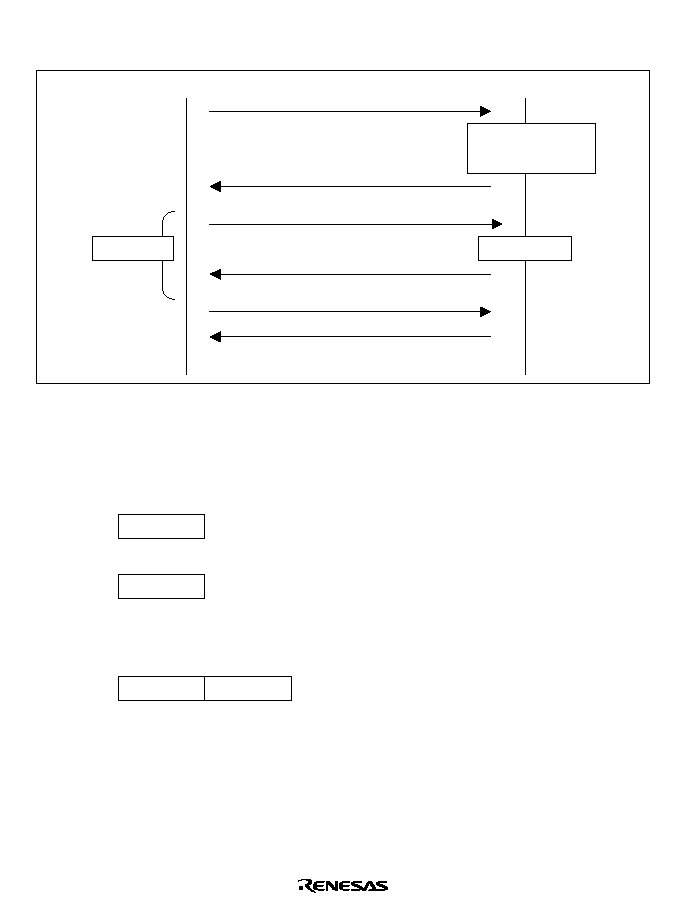
665
The sequences of the issuing of erasure selection commands and the erasure of data are shown in
figure 18.28.
Transfer of Erasure
Program
Host
Boot Program
Preparation for Erasure (H'48)
ACK
Erasure
Erasure (Erased Block Number)
Erasure (H'FF)
ACK
ACK
Repeat
Figure 18.28 Erasure Sequence
(1) Erasure Selection
The boot program will transfer the erasure program. User MAT data is erased by the transferred
erasure program.
Command
H'48
Command, H'48, (1 byte) : Erasure selection
Response
H'06
Response, H'06, (1 byte) : Response for erasure selection
After the erasure program has been transferred, the boot program will return ACK.
Error
response
H'C8
ERROR
Error response: H'C8 (1 byte): Error response to erasing selection
ERROR: (1 byte): Error code
H'54: Selection processing error (transfer error occurs and processing is not completed)
(2) Block Erasure
The boot program will erase the contents of the specified block.

666
Command
H'58
Size
Block Number
SUM
Command, H'58, (1 byte) : Erasure
Size (1 byte) : The number of bytes that represents the erasure block number
This is fixed to 1.
Block Number (1 byte) : Number of the block to be erased
SUM (1 byte) : Checksum
Response
H'06
Response, H'06, (1 byte) : Response to Erasure
After erasure has been completed, the boot program will return ACK.
Error
response
H'D8
ERROR
Error Response, H'D8, (1 byte) : Error code
ERROR (1 byte) : Error code
H'11 : Sum check error
H'29 : Block number error
Block number is incorrect.
H'51 : Erasure error
An error has occurred during erasure.
On receiving block number H'FF, the boot program will stop erasure and wait for a
selection command.
Command
H'58
Size
Block Number
SUM
Command, H'58, (1 byte) : Erasure
Size (1 byte) : The number of bytes that represents the block number
This is fixed to 1.
Block Number (1 byte) : H'FF
Stop code for erasure
SUM (1 byte) : Checksum
Response
H'06
Response, H'06, (1 byte) : Response to end of erasure (ACK)
When erasure is to be performed after the block number H'FF has been sent, the procedure
should be executed from the erasure selection command.
�
Memory read
The boot program will return the data in the specified address.
667
Command
H'52
Size
Area
Read address
Read size
SUM
Command: H'52 (1 byte): Memory read
Size (1 byte): Amount of data that represents the area, read address, and read size (fixed at
9)
Area (1 byte)
H'00 : User boot MAT
H'01 : User MAT
An address error occurs when the area setting is incorrect.
Read address (4 bytes): Start address to be read from
Read size (4 bytes): Size of data to be read
SUM (1 byte): Checksum
Response
H'52
Read size
Data
���
SUM
Response: H'52 (1 byte): Response to memory read
Read size (4 bytes): Size of data to be read
Data (n bytes): Data for the read size from the read address
SUM (1 byte): Checksum
Error
response
H'D2
ERROR
Error response: H'D2 (1 byte): Error response to memory read
ERROR: (1 byte): Error code
H'11: Sum check error
H'2A: Address error
The read address is not in the MAT.
H'2B: Size error
The read size exceeds the MAT.
�
User-Boot Program Sum check
The boot program will return the byte-by-byte total of the contents of the bytes of the user-boot
program.
Command
H'4A
Command, H'4A, (1 byte) : Sum check for user-boot program
Response
H'5A
Size
Checksum of user boot program
SUM
Response, H'5A, (1 byte) :
Response to the sum check of user-boot program

668
Size (1 byte) : The number of bytes that represents the checksum
This is fixed to 4.
Checksum of user boot program (4 bytes) : Checksum of user boot MATs
The total of the data is obtained in byte units.
SUM (1 byte) : Sum check for data being transmitted
�
User-Program Sum check
The boot program will return the byte-by-byte total of the contents of the bytes of the user
program.
Command
H'4B
Command, H'4B, (1 byte) : Sum check for user program
Response
H'5B
Size
Checksum of user program
SUM
Response, H'5B, (1 byte) : Response to the sum check of the user program
Size (1 byte) : The number of bytes that represents the checksum
This is fixed to 4.
Checksum of user boot program (4 bytes) : Checksum of user MATs
The total of the data is obtained in byte units.
SUM (1 byte) : Sum check for data being transmitted
�
User Boot MAT Blank check
The boot program will check whether or not all user boot MATs are blank and return the result.
Command
H'4C
Command, H'4C, (1 byte) : Blank check for user boot MAT
Response
H'06
Response, H'06, (1 byte) : Response to the blank check of user boot MAT
If all user MATs are blank (H'FF), the boot program will return ACK.
Error
response
H'CC
H'52
Error Response, H'CC, (1 byte) : Response to blank check for user boot MAT
Error Code, H'52, (1 byte)
: Erasure has not been completed.
�
User MAT Blank Check
The boot program will check whether or not all user MATs are blank and return the result.
Command
H'4D
Command, H'4D, (1 byte) : Blank check for user MATs

669
Response
H'06
Response, H'06, (1 byte) : Response to the blank check for user boot MATs
If the contents of all user MATs are blank (H'FF), the boot program will return ACK.
Error
response
H'CD
H'52
Error Response, H'CD, (1 byte) : Error response to the blank check of user MATs.
Error code H'52 (1 byte) : Erasure has not been completed.
�
Boot Program State Inquiry
The boot program will return indications of its present state and error condition. This inquiry can
be made in the inquiry/selection state or the programming/erasing state.
Command
H'4F
Command, H'4F, (1 byte) : Inquiry regarding boot program's state
Response
H'5F
Size
STATUS
ERROR
SUM
Response, H'5F, (1 byte) : Response to boot program state inquiry
Size (1 byte) : The number of bytes that represents the STATUS and ERROR.
This is fixed to 2.
STATUS (1 byte) : State of the boot program
For details, see table 18.18.
ERROR (1 byte): Error state
ERROR = 0 indicates normal operation.
ERROR = 1 indicates error has occurred
For details, see table 18.19.
SUM (1 byte): Checksum

670
Table 18.18 Status Code
Code
Description
H'11
Device Selection Wait
H'12
Clock Mode Selection Wait
H'13
Bit Rate Selection Wait
H'1F
Programming/Erasing State Transition Wait (Bit rate selection is completed)
H'31
Programming State for Erasure
H'3F
Programming/Erasing Selection Wait (Erasure is completed)
H'4F
Programming Data Receive Wait (Programming is completed)
H'5F
Erasure Block Specification Wait (Erasure is completed)
Table 18.19 Error Code
Code
Description
H'00
No Error
H'11
Sum Check Error
H'12
Program Size Error
H'21
Device Code Mismatch Error
H'22
Clock Mode Mismatch Error
H'24
Bit Rate Selection Error
H'25
Input Frequency Error
H'26
Multiplication Ratio Error
H'27
Operating Frequency Error
H'29
Block Number Error
H'2A
Address Error
H'2B
Data Length Error
H'51
Erasure Error
H'52
Erasure Incompletion Error
H'53
Programming Error
H'54
Selection Error
H'80
Command Error
H'FF
Bit-Rate-Adjustment Confirmation Error
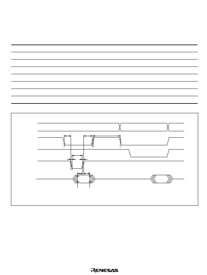
671
18.10.2
AC Characteristics and Timing in Writer Mode
Table 18.20 AC Characteristics in Memory Read Mode
Condition : V
CC
= 5.0 V
�
0.5 V, V
SS
= 0 V, T
a
= 25�C
�
5�C
Code
Symbol
Min
Max
Unit
Note
Command write cycle
t
nxtc
20
�
s
CE
hold time
t
ceh
0
ns
CE
setup time
t
ces
0
ns
Data hold time
t
dh
50
ns
Data setup time
t
ds
50
ns
Programming pulse width
t
wep
70
ns
WE
rise time
t
r
30
ns
WE
fall time
t
f
30
ns
CE
A18-0
I/O7-0
OE
WE
Command write
t
ceh
t
ds
t
dh
tf
tr
t
nxtc
Note : Data is latched at the rising edge of
WE
.
t
ces
t
wep
Memory read mode
Address stable
Figure 18.29 Memory Read Timing after Command Write
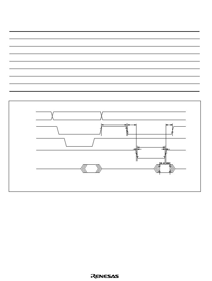
672
Table 18.21 AC Characteristics in Transition from Memory Read Mode to Others
Condition : V
CC
= 5.0 V
�
0.5 V, V
SS
= 0 V, T
a
= 25�C
�
5�C
Code
Symbol
Min
Max
Unit
Note
Command write cycle
t
nxtc
20
�
s
CE
hold time
t
ceh
0
ns
CE
setup time
t
ces
0
ns
Data hold time
t
dh
50
ns
Data setup time
t
ds
50
ns
Programming pulse width
t
wep
70
ns
WE
rise time
t
r
30
ns
WE
fall time
t
f
30
ns
CE
A18-0
I/O7-0
OE
WE
Other Mode Command Write
t
ceh
t
ds
t
dh
tf
tr
t
nxtc
Note :
WE
and
OE
should not be enabled simultaneously.
t
ces
t
wep
Memory Read Mode
Address Stable
Figure 18.30 Timing at Transition from Memory Read Mode to Other Modes
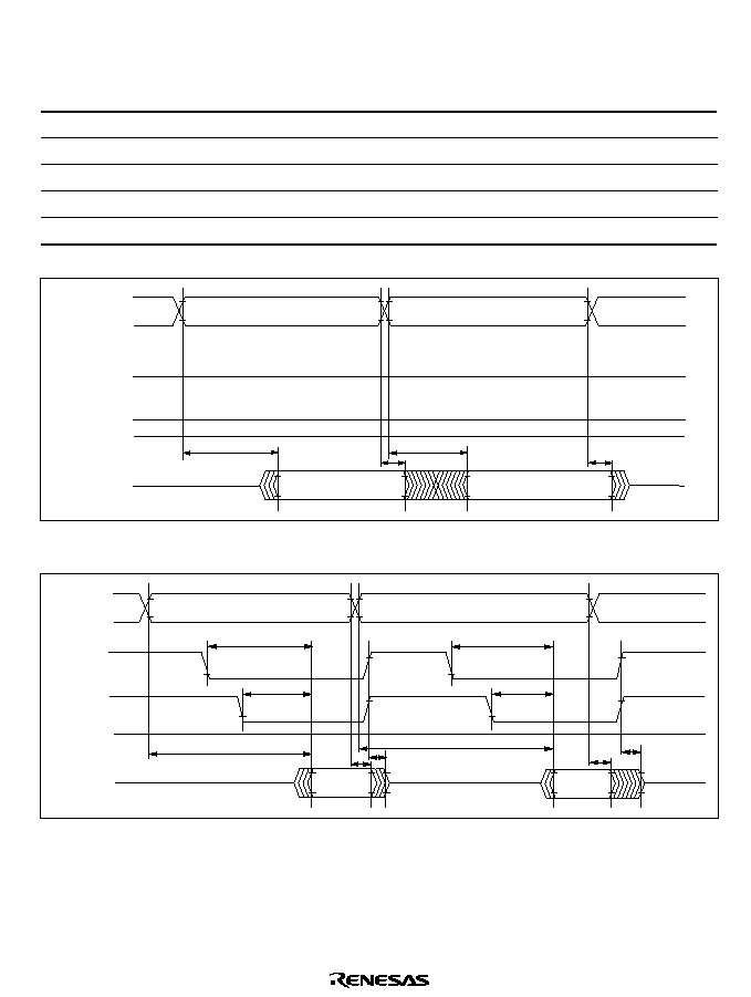
673
Table 18.22 AC Characteristics Memory Read Mode
Condition : V
CC
= 5.0 V
�
0.5 V, V
SS
= 0 V, T
a
= 25�C
�
5�C
Code
Symbol
Min
Max
Unit
Note
Access time
t
acc
20
�
s
CE
output delay time
t
ce
150
ns
OE
output delay time
t
oe
150
ns
Output disable delay time
t
df
100
ns
Data output hold time
t
oh
5
ns
CE
A18-0
I/O7-0
OE
WE
V
IH
V
IL
V
IL
t
acc
t
oh
t
oh
t
acc
Address Stable
Address Stable
Figure 18.31
CE/OE Enable State Read
CE
A18-0
I/O7-0
V
IH
OE
WE
t
ce
t
acc
t
oe
t
oh
t
oh
t
df
t
ce
t
acc
t
oe
Address Stable
Address Stable
t
df
Figure 18.32
CE/OE Clock Read
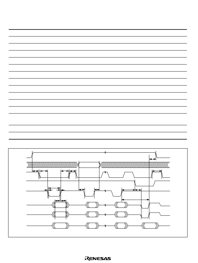
674
Table 18.23 AC Characteristics Auto-Write Mode
Condition : V
CC
= 5.0 V
�
0.5 V, V
SS
= 0 V, T
a
= 25�C
�
5�C
Code
Symbol
Min
Max
Unit
Note
Command write cycle
t
nxtc
20
�
s
CE
hold time
t
ceh
0
ns
CE
setup time
t
ces
0
ns
Data hold time
t
dh
50
ns
Data setup time
t
ds
50
ns
Programming pulse width
t
wep
70
ns
Status polling start time
t
wsts
1
ms
Status polling access time
t
spa
150
ns
Address setup time
t
as
0
ns
Address hold time
t
ah
60
ns
Memory programming time
t
write
1
3000
ms
Programming setup time
t
pns
100
ns
Programming end setup
time
t
pnh
100
ns
WE
rise time
t
r
30
ns
WE
fall time
t
f
30
ns
Address Stable
CE
FWE
A18-0
I/O5-0
I/O6
I/O7
OE
WE
t
as
t
ah
t
dh
t
ds
tf
tr
t
wep
t
wsts
t
write
t
spa
t
pns
t
pnh
t
nxtc
t
nxtc
t
ceh
t
ces
Identification Signal of
Programming Operation End
Data Transfer
1 byte to 128 bytes
Identification Signal of
Programming Operation
Successful End
H'40 or
H'45
1st byte
Din
128th byte
Din
H'00
Figure 18.33 Timing in Auto-Write Mode
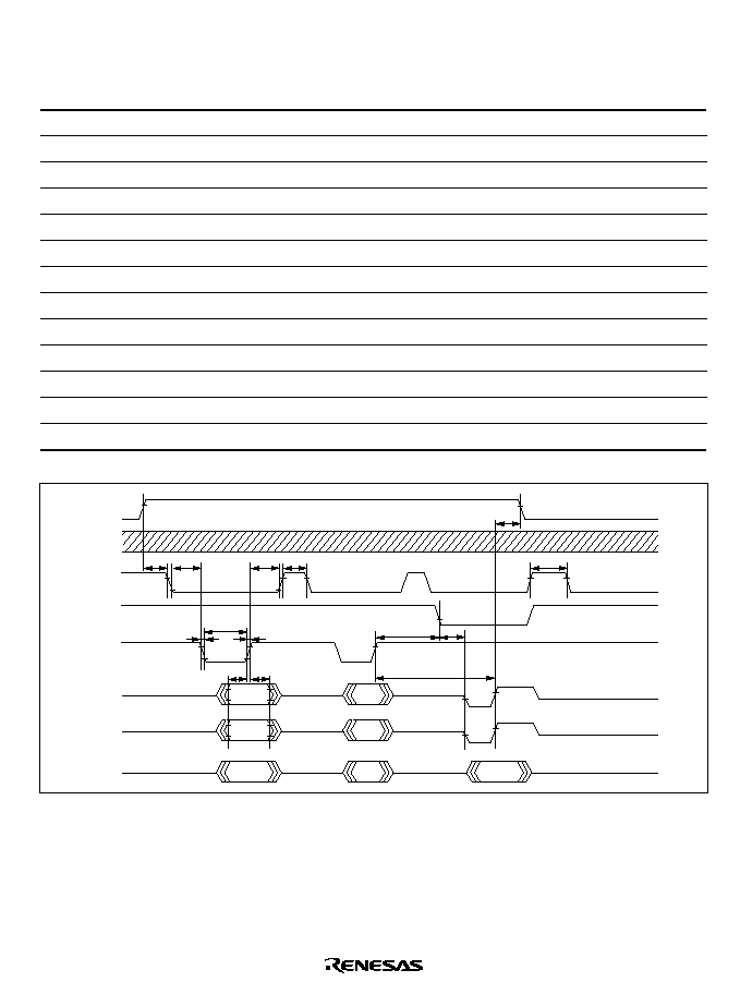
675
Table 18.24 AC Characteristics Auto-Erase Mode
Condition : V
CC
= 5.0 V
�
0.5 V, V
SS
= 0 V, T
a
= 25�C
�
5�C
Code
Symbol
Min
Max
Unit
Note
Command write cycle
t
nxtc
20
�
s
CE
hold time
t
ceh
0
ns
CE
setup time
t
ces
0
ns
Data hold time
t
dh
50
ns
Data setup time
t
ds
50
ns
Programming pulse width
t
wep
70
ns
Status polling start time
t
ests
1
ms
Status polling access time
t
spa
150
ns
Memory erase time
t
erase
100
40000
ms
Erase setup time
t
ens
100
ns
Erase end setup time
t
enh
100
ns
WE
rise time
t
r
30
ns
WE
fall time
t
f
30
ns
CE
FWE
A18-0
I/O5-0
I/O6
I/O7
OE
WE
t
ests
t
erase
t
spa
t
dh
t
ds
tf
tr
t
wep
t
ens
t
enh
t
nxtc
t
nxtc
t
ceh
t
ces
Erase end
identification
signal
Erase normal
and confirmation
signal
H'20 or
H'25
H'20 or
H'25
H'00
Figure 18.34 Timing in Auto-Erase Mode
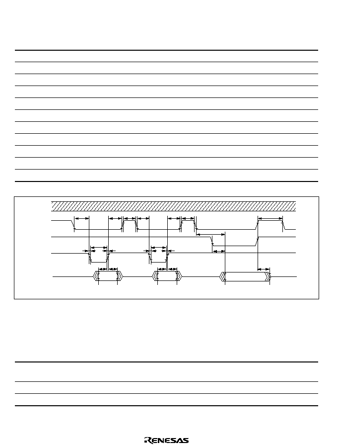
676
Table 18.25 AC Characteristics Status Read Mode
Condition : V
CC
= 5.0 V
�
0.5 V, V
SS
= 0 V, T
a
= 25�C
�
5�C
Code
Symbol
Min
Max
Unit
Note
Command write cycle
t
nxtc
20
�
s
CE
hold time
t
ceh
0
ns
CE
setup time
t
ces
0
ns
Data hold time
t
dh
50
ns
Data setup time
t
ds
50
ns
Programming pulse width
t
wep
70
ns
OE
output delay time
t
oe
150
ns
Disable delay time
t
df
100
ns
CE
output delay time
t
ce
150
ns
WE
rise time
t
r
30
ns
WE
fall time
t
f
30
ns
CE
A18-0
I/O7-0
OE
WE
t
dh
t
df
t
ds
tf
tr
t
wep
t
nxtc
t
nxtc
tf
tr
t
wep
t
ds
t
dh
t
nxtc
t
ceh
t
ceh
t
oe
t
ces
t
ces
t
ce
H'71
H'71
Note: I/O3 and I/O2 are undefined.
Figure 18.35 Timing in Status Read Mode
Table 18.26 Stipulated Transition Times to Command Wait State
Condition : V
CC
= 5.0 V
�
0.5 V, V
SS
= 0 V, T
a
= 25�C
�
5�C
Code
Symbol
Min
Max
Unit
Note
Standby release
(oscillation settling time)
t
osc1
30
ms
PROM mode setup time
t
bmv
10
ms
V
CC
hold time
t
dwn
0
ms
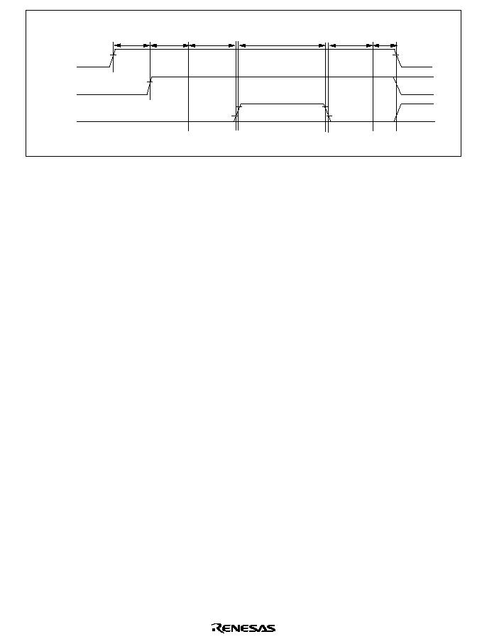
677
V
CC
RES
FWE
Memory read mode
Command wait state
Command wait state
Normal/abnormal
end identification
Auto-program mode
Auto-erase mode
t
osc1
t
bmv
t
dwn
Note: Set the FWE input pin low level, except in the auto-program and auto-erase modes.
Figure 18.36 Oscillation Stabilization Time, PROM Mode Setup Time, and
Power-Down Sequence
18.10.3 Procedure Program and Storable Area for Programming Data
In the descriptions in the previous section, the programming/erasing procedure programs and
storable areas for program data are assumed to be in the on-chip RAM. However, the program
and the data can be stored in and executed from other areas, such as part of flash memory which is
not to be programmed or erased, or somewhere in the external address space.
�
Conditions that Apply to Programming/Erasing
(1) The on-chip programming/erasing program is downloaded from the address set by FTDAR in
on-chip RAM, therefore, this area is not available for use.
(2) The on-chip programming/erasing program will use the 128 bytes as a stack. So, make sure
that this area is secured.
(3) Since download by setting the SCO bit to 1 will cause the MATs to be switched, it should be
executed in on-chip RAM.
(4) The flash memory is accessible until the start of programming or erasing, that is, until the
result of downloading has been judged. When in a mode in which the external address space is
not accessible, such as single-chip mode, the required procedure programs, NMI handling
vector, NMI handler and user branch program should be transferred to the on-chip RAM
before programming/erasing of the flash memory starts.
(5) The flash memory is not accessible during programming/erasing operations, therefore, the
operation program is downloaded to the on-chip RAM to be executed. The NMI-handling
vector and programs such as that which activate the operation program, user program at the
user-branch destination during programming/erasing operation, and NMI handler should thus
be stored in on-chip memory other than flash memory or the external address space.
(6) After programming/erasing, the flash memory should be inhibited until FKEY is cleared.
The reset state (
RES = 0) must be in place for more than 100
�
s when the LSI mode is changed
to reset on completion of a programming/erasing operation.

678
Transitions to the reset state, and hardware standby mode are inhibited during
programming/erasing. When the reset signal is accidentally input to the chip, a longer period
in the reset state than usual (100
�
s) is needed before the reset signal is released.
(7) Switching of the MATs by FMATS should be needed when programming/erasing of the user
boot MAT is operated in user-boot mode. The program which switches the MATs should be
executed from the on-chip RAM. See section 18.8, Switching between User MAT and User
Boot MAT. Please make sure you know which MAT is selected when switching between
them.
(8) When the data storable area indicated by programming parameter FMPDR is within the flash
memory area, an error will occur even when the data stored is normal. Therefore, the data
should be transferred to the on-chip RAM to place the address that FMPDR indicates in an
area other than the flash memory.
In consideration of these conditions, there are three factors; operating mode, the bank structure of
the user MAT, and operations.
The areas in which the programming data can be stored for execution are shown in table 18.27.
Table 18.27 Executable MAT
Initiated Mode
Operation
User Program Mode
User Boot Mode
*
Programming
Table 18.28 (1)
Table 18.28 (3)
Erasing
Table 18.28 (2)
Table 18.28 (4)
Note :
*
Programming/Erasing is possible to user MATs.
679
Table 18.28 (1) Useable Area for Programming in User Program Mode
Storable /Executable Area
Selected MAT
Item
On-chip
RAM
User
MAT
External Space
(Expanded Mode)
User
MAT
Embedded
Program Storage
Area
Programming
Procedure
Storage Area for
Program Data
�
*
--
--
Operation for
Selection of On-
chip Program to
be Downloaded
Operation for
Writing H'A5 to
Key Register
Execution of
Writing SC0 = 1
to FCCS
(Download)
�
�
Operation for
Key Register
Clear
Judgement of
Download
Result
Operation for
Download Error
Operation for Settings of Initial
Parameter
Execution of Initialization
�
�
Judgement of Initialization
Result
Operation for Initialization Error

680
Storable /Executable Area
Selected MAT
Item
On-chip
RAM
User
MAT
External Space
(Expanded Mode)
User
MAT
Embedded
Program Storage
Area
NMI Handling Routine
�
Operation for Inhibit of Interrupt
Operation for Writing H'5A to
Key Register
Operation for Settings of
Program Parameter
�
Execution of Programming
�
�
Judgement of Program Result
�
Operation for Program Error
�
Operation for Key Register
Clear
�
Note :
*
Transferring the data to the on-chip RAM enables this area to be used.
681
Table 18.28 (2) Useable Area for Erasure in User Program Mode
Storable /Executable Area
Selected MAT
Item
On-chip
RAM
User
MAT
External Space
(Expanded Mode)
User
MAT
Embedded
Program Storage
Area
Erasing
Procedure
Operation for
Selection of On-
chip Program to
be Downloaded
Operation for
Writing H'A5 to
Key Register
Execution of
Writing SC0 = 1
to FCCS
(Download)
�
�
Operation for
Key Register
Clear
Judgement of
Download
Result
Operation for Download Error
Operation for Settings of
Default Parameter
Execution of Initialization
�
�
Judgement of Initialization
Result
Operation for Initialization Error
NMI Handling Routine
�
682
Storable /Executable Area
Selected MAT
Item
On-chip
RAM
User
MAT
External Space
(Expanded Mode) User
MAT
Embedded
Program Storage
Area
Operation for Inhibit of Interrupt
Operation for Writing H'5A to
Key Register
Operation for Settings of
Erasure Parameter
�
Execution of Erasure
�
�
Judgement of Erasure Result
�
Operation for Erasure Error
�
Operation for Key Register
Clear
�
683
Table 18.28 (3) Useable Area for Programming in User Boot Mode
Storable/Executable Area
Selected MAT
Item
On-chip
RAM
User
Boot
MAT
External Space
(Expanded
Mode)
User
MAT
User
Boot
MAT
Embedded
Program
Storage Area
Programming
procedure
Storage Area for
Program Data
�
*
1
--
--
--
Operation for
Selection of On-
chip Program to
be Downloaded
Operation for
Writing H'A5 to
Key Register
Execution of
Writing SC0 = 1
to FCCS
(Download)
�
�
Operation for
Key Register
Clear
Judgement of
Download
Result
Operation for
Download Error
Operation for Settings of
Default Parameter
Execution of Initialization
�
�
Judgement of Initialization
Result
Operation for Initialization Error
NMI Handling Routine
�

684
Storable/Executable Area
Selected MAT
Item
On-chip
RAM
User
Boot
MAT
External Space
(Expanded
Mode)
User
MAT
User
Boot
MAT
Embedded
Program
Storage Area
Operation for Interrupt Inhibit
Switching MATs by FMATS
�
�
Operation for Writing H'5A to
Key Register
�
Operation for Settings of
Program Parameter
�
Execution of Programming
�
�
Judgement of Program Result
�
Operation for Program Error
�
*
2
Operation for Key Register
Clear
�
Switching MATs by FMATS
�
�
Notes:
*
1 Transferring the data to the on-chip RAM enables this area to be used.
*
2 Switching FMATS by a program in the on-chip RAM enables this area to be used.
685
Table 18.28 (4) Useable Area for Erasure in User Boot Mode
Storable/Executable Area
Selected MAT
Item
On-chip
RAM
User
Boot
MAT
External Space
(Expanded
Mode)
User
MAT
User
Boot
MAT
Embedded
Program
Storage Area
Erasing
Procedure
Operation for
Selection of On-
chip Program to
be Downloaded
Operation for
Writing H'A5 to
Key Register
Execution of
Writing SC0 = 1
to FCCS
(Download)
�
�
Operation for
Key Register
Clear
Judgement of
Download
Result
Operation for Download Error
Operation for Settings of
Default Parameter
Execution of Initialization
�
�
Judgement of Initialization
Result
Operation for Initialization Error
NMI Handling Routine
�
686
Storable/Executable Area
Selected MAT
Item
On-chip
RAM
User
Boot
MAT
External Space
(Expanded
Mode)
User
MAT
User
Boot
MAT
Embedded
Program
Storage Area
Operation for Interrupt Inhibit
Switching MATs by FMATS
�
�
Operation for Writing H'5A to
Key Register
�
Operation for Settings of
Erasure Parameter
�
Execution of Erasure
�
�
Judgement of Erasure Result
�
Operation for Erasure Error
�
*
Operation for Key Register
Clear
�
Switching MATs by FMATS
�
�
Note:
*
Switching FMATS by a program in the on-chip RAM enables this area to be used.
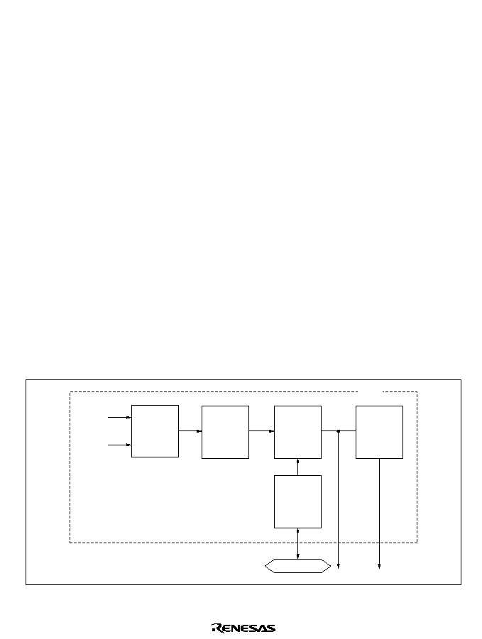
687
Section 19 Clock Pulse Generator
19.1
Overview
The H8/3069F has a built-in clock pulse generator (CPG) that generates the system clock (
) and
other internal clock signals (
/2 to
/4096). After duty adjustment, a frequency divider divides the
clock frequency to generate the system clock (
). The system clock is output at the
pin*
1
and
furnished as a master clock to prescalers that supply clock signals to the on-chip supporting
modules. Frequency division ratios of 1/1, 1/2, 1/4, and 1/8 can be selected for the frequency
divider by settings in a division control register (DIVCR)*
2
. Power consumption in the chip is
reduced in almost direct proportion to the frequency division ratio.
Notes: *1 Usage of the
pin differs depending on the chip operating mode and the PSTOP bit
setting in the module standby control register (MSTCR). For details, see section 20.7,
System Clock Output Disabling Function.
*2 The division ratio of the frequency divider can be changed dynamically during
operation. The clock output at the
pin also changes when the division ratio is
changed. The frequency output at the
pin is shown below.
= EXTAL
�
n
where, EXTAL: Frequency of crystal resonator or external clock signal
n:
Frequency division ratio (n = 1/1, 1/2, 1/4, or 1/8)
19.1.1
Block Diagram
Figure 19.1 shows a block diagram of the clock pulse generator.
XTAL
EXTAL
CPG
pin
/2 to
/4096
Oscillator
Duty
adjustment
circuit
Frequency
divider
Division
control
register
Prescalers
Data bus
Figure 19.1 Block Diagram of Clock Pulse Generator
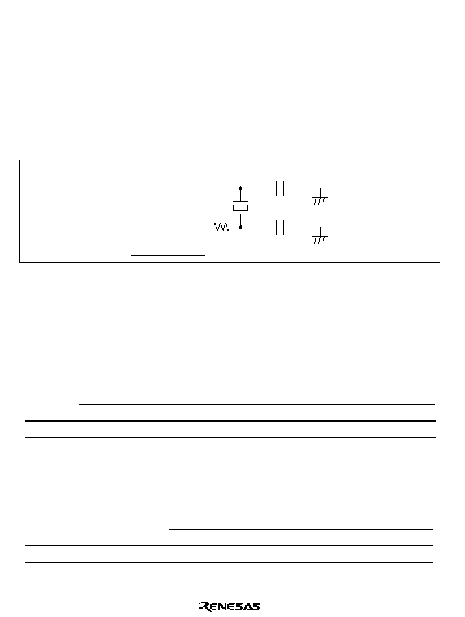
688
19.2
Oscillator Circuit
Clock pulses can be supplied by connecting a crystal resonator, or by input of an external clock
signal.
19.2.1
Connecting a Crystal Resonator
Circuit Configuration: A crystal resonator can be connected as in the example in figure 19.2.
Damping resistance Rd should be selected according to table 19.1 (1), and external capacitances
C
L1
and C
L2
according to table 19.1 (2). An AT-cut parallel-resonance crystal should be used.
EXTAL
XTAL
C
L1
C
L2
Rd
Figure 19.2 Connection of Crystal Resonator (Example)
If a crystal resonator with a frequency higher than 20 MHz is connected, the external load
capacitance values in table 19.1 (2) should not exceed 10 pF. Also, in order to improve the
accuracy of the oscillation frequency, a thorough study of oscillation matching evaluation, etc.,
should be carried out when deciding the circuit constants.
Table 19.1 (1) Damping Resistance Value
Damping
Resistance
Frequency f (MHz)
Value
10
f
13
13
<
f
16
16
<
f
18
18
<
f
25
Rd (
)
0
0
0
0
Note:
A crystal resonator between 10 MHz and 25 MHz can be used. If the chip is to be operated
at less than 10 MHz, the on-chip frequency divider should be used. (A crystal resonator of
less than 10 MHz cannot be used.)
Table 19.1 (2) External Capacitance Values
Frequency f (MHz)
External Capacitance Value
20
<
f
25
10
f
20
C
L1
= C
L2
(pF)
10
10 to 22
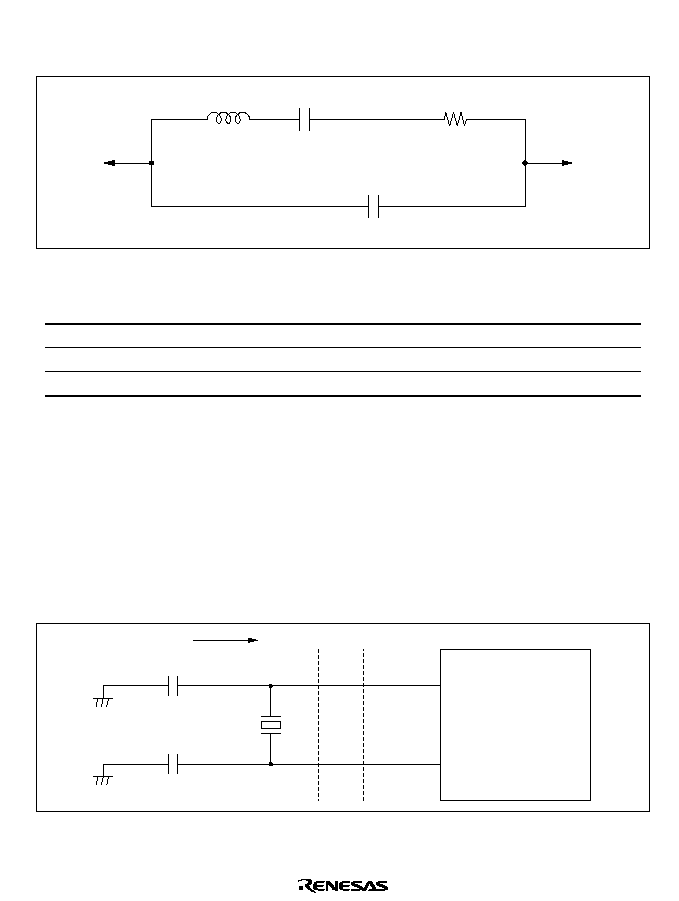
689
Crystal Resonator: Figure 19.3 shows an equivalent circuit of the crystal resonator. The crystal
resonator should have the characteristics listed in table 19.2.
XTAL
L
Rs
C
L
C
0
EXTAL
AT-cut parallel-resonance type
Figure 19.3 Crystal Resonator Equivalent Circuit
Table 19.2
Crystal Resonator Parameters
Frequency (MHz)
10
12
16
18
20
25
Rs max (
)
30
30
20
20
20
20
Co (pF)
7 (max)
7 (max)
7 (max)
7 (max)
7 (max)
7 (max)
Use a crystal resonator with a frequency equal to the system clock frequency (
).
Notes on Board Design: When a crystal resonator is connected, the following points should be
noted:
Other signal lines should be routed away from the oscillator circuit to prevent induction from
interfering with correct oscillation. See figure 19.4.
When the board is designed, the crystal resonator and its load capacitors should be placed as close
as possible to the XTAL and EXTAL pins.
XTAL
EXTAL
C
L2
C
L1
H8/3069F chip
Avoid
Signal A
Signal B
Figure 19.4 Oscillator Circuit Block Board Design Precautions
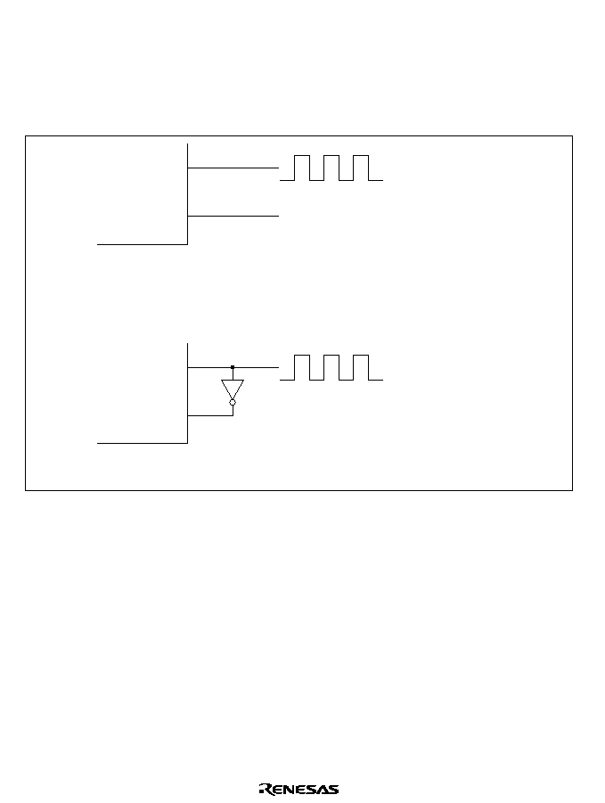
690
19.2.2
External Clock Input
Circuit Configuration: An external clock signal can be input as shown in the examples in figure
19.5. If the XTAL pin is left open, the stray capacitance should not exceed 10 pF. If the stray
capacitance at the XTAL pin exceeds 10 pF in configuration a, use the connection shown in
configuration b instead, and hold the external clock high in standby mode.
EXTAL
XTAL
EXTAL
XTAL
External clock input
Open
External clock input
a. XTAL pin left open
b. Complementary clock input at XTAL pin
Figure 19.5 External Clock Input (Examples)
External Clock: The external clock frequency should be equal to the system clock frequency
when not divided by the on-chip frequency divider. Table 19.3 shows the clock timing, figure 19.6
shows the external clock input timing, and figure 19.7 shows the external clock output settling
delay timing. When the appropriate external clock is input via the EXTAL pin, its waveform is
corrected by the on-chip oscillator and duty adjustment circuit.
When the appropriate external clock is input via the EXTAL pin, its waveform is corrected by the
on-chip oscillator and duty adjustment circuit. The resulting stable clock is output to external
devices after the external clock settling time (t
DEXT
) has passed after the clock input. The system
must remain reset with the reset signal low during t
DEXT
, while the clock output is unstable.
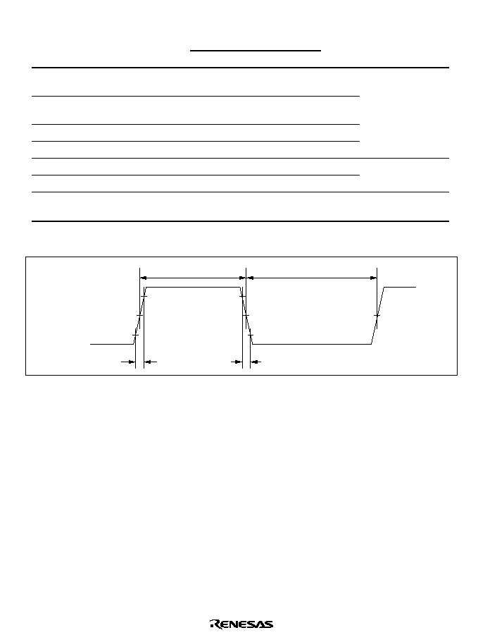
691
Table 19.3
Clock Timing
V
CC
= 5.0 V
�
10%
Item
Symbol Min
Max
Unit
Test Conditions
External clock input low
pulse width
t
EXL
15
--
ns
Figure 19.6
External clock input high
pulse width
t
EXH
15
--
ns
External clock rise time
t
EXr
--
5
ns
External clock fall time
t
EXf
--
5
ns
Clock low pulse width
t
CL
0.4
0.6
t
cyc
Figure 21.7
Clock high pulse width
t
CH
0.4
0.6
t
cyc
External clock output
settling delay time
t
DEXT
*
500
--
�
s
Figure 19.7
Note:
*
t
DEXT
includes a
RES
pulse width (t
RESW
). t
RESW
= 20 t
cyc
EXTAL
t
EXr
t
EXf
V
CC
�
0.7
0.3 V
t
EXH
t
EXL
V
CC
�
0.5
Figure 19.6 External Clock Input Timing
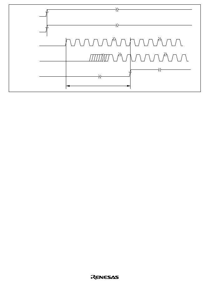
692
V
CC
STBY
EXTAL
(internal or
external)
RES
t
DEXT
V
IH
Figure 19.7 External Clock Output Settling Delay Timing
19.3
Duty Adjustment Circuit
When the oscillator frequency is 5 MHz or higher, the duty adjustment circuit adjusts the duty
cycle of the clock signal from the oscillator to generate
.
19.4
Prescalers
The prescalers divide the system clock (
) to generate internal clocks (
/2 to
/4096).
19.5
Frequency Divider
The frequency divider divides the duty-adjusted clock signal to generate the system clock (
). The
frequency division ratio can be changed dynamically by modifying the value in DIVCR, as
described below. Power consumption in the chip is reduced in almost direct proportion to the
frequency division ratio. The system clock generated by the frequency divider can be output at the
pin.
693
19.5.1
Register Configuration
Table 19.4 summarizes the frequency division register.
Table 19.4
Frequency Division Register
Address
*
Name
Abbreviation
R/W
Initial Value
H'EE01B
Division control register
DIVCR
R/W
H'FC
Note:
*
Lower 20 bits of the address in advanced mode.
19.5.2
Division Control Register (DIVCR)
DIVCR is an 8-bit readable/writable register that selects the division ratio of the frequency
divider.
Bit
Initial value
Read/Write
7
--
1
--
6
--
1
--
5
--
1
--
4
--
1
--
3
--
1
--
0
DIV0
0
R/W
2
--
1
--
1
DIV1
0
R/W
Reserved bits
Divide bits 1 and 0
These bits select the
frequency division ratio
DIVCR is initialized to H'FC by a reset and in hardware standby mode. It is not initialized in
software standby mode.
Bits 7 to 2--Reserved: These bits cannot be modified and are always read as 1.
Bits 1 and 0--Divide (DIV1, DIV0): These bits select the frequency division ratio, as follows.
Bit 1
DIV1
Bit 0
DIV0
Frequency Division Ratio
0
0
1/1
(Initial value)
0
1
1/2
1
0
1/4
1
1
1/8

694
19.5.3
Usage Notes
The DIVCR setting changes the
frequency, so note the following points.
�
Select a frequency division ratio that stays within the assured operation range specified for the
clock cycle time t
cyc
in the AC electrical characteristics. Note that
min
= lower limit of the
operating frequency range. Ensure that � is not below this lower limit.
�
All on-chip module operations are based on
. Note that the timing of timer operations, serial
communication, and other time-dependent processing differs before and after any change in the
division ratio. The waiting time for exit from software standby mode also changes when the
division ratio is changed. For details, see section 20.4.3, Selection of Waiting Time for Exit
from Software Standby Mode.

695
Section 20 Power-Down State
20.1
Overview
The H8/3069F has a power-down state that greatly reduces power consumption by halting the
CPU, and a module standby function that reduces power consumption by selectively halting on-
chip modules.
The power-down state includes the following three modes:
�
Sleep mode
�
Software standby mode
�
Hardware standby mode
The module standby function can halt on-chip supporting modules independently of the power-
down state. The modules that can be halted are the 16-bit timer, 8-bit timer, SCI0, SCI1, SCI2,
DMAC, DRAM interface, and A/D converter.
Table 20.1 indicates the methods of entering and exiting the power-down modes and module
standby mode, and gives the status of the CPU and on-chip supporting modules in each mode.

696
Table 20.1
Power-Down State and Module Standby Function
Cloc
k
Activ
e
Halted
Halted
Activ
e
Exiting
Conditions
�
Interr
upt
�
RES
�
STBY
�
NMI
�
IRQ
0
to IRQ
2
�
RES
�
STBY
�
STBY
�
RES
�
STBY
�
RES
�
Clear MSTCR
bit to 0
*
5
I/O
Po
r
t
s
Held
Held
High
impedance
--
c
loc
k
output
output
High
output
High
impedance
High
impedance
*
2
RAM
Held
Held
Held
*
3
--
Other
Modules
Activ
e
Halted
and
reset
Halted
and
reset
Activ
e
DRAM
Interface
Activ
e
Halted
and
held
*
1
Halted
and
reset
Halted
*
2
and
held
*
1
DMA
C
Activ
e
Halted
and
reset
Halted
and
reset
Halted
*
2
and
reset
CPU
Register
s
Held
Held
Undeter-
mined
--
CPU
Halted
Halted
Halted
Activ
e
Entering
Conditions
SLEEP instr
uc-
tion e
x
ecuted
while SSBY = 0
in SYSCR
SLEEP instr
uc-
tion e
x
ecuted
while SSBY = 1
in SYSCR
Lo
w input at
STBY pin
Corresponding
bit set to 1 in
MSTCR
Mode
Sleep
mode
Softw
are
standb
y
mode
Hardw
are
standb
y
mode
Module
standb
y
16-Bit
Timer
Activ
e
Halted
and
reset
Halted
and
reset
Halted
*
2
and
reset
8-Bit
Timer
Activ
e
Halted
and
reset
Halted
and
reset
Halted
*
2
and
reset
SCI0
Activ
e
Halted
and
reset
Halted
and
reset
Halted
*
2
and
reset
SCI1
Activ
e
Halted
and
reset
Halted
and
reset
Halted
*
2
and
reset
SCI2
Activ
e
Halted
and
reset
Halted
and
reset
Halted
*
2
and
reset
A/D
Activ
e
Halted
and
reset
Halted
and
reset
Halted
*
2
and
reset
State
Notes:
*
1
R
TCNT and bits 7 and 6 of R
TMCSR are initializ
ed.
Other bits and registers hold their pre
vious states
.
*
2
State in which the corresponding MSTCR bit w
as set to 1.
F
or details see section 20.2.2, Module Standb
y Control Register H (MS
TCRH) and section 20.2.3,
Module Standb
y Control Register L (MSTCRL).
*
3
The RAME bit m
ust be cleared to 0 in SYSCR bef
ore the tr
ansition from the prog
r
am e
x
ecution state to hardw
are standb
y mode
.
*
4
When P6
7
is used as the
output pin.
*
5
When a MSTCR bit is set to 1, the registers of the corresponding on-chip suppor
ting module are initializ
ed.
T
o
restar
t the mod
ule
, first clear the MSTCR bit to 0,
then set up the module registers again.
Legend
SYSCR:
System control register
SSBY
:
Softw
are standb
y bit
MSTCRH:
Module standb
y control register H
MSTCRL:
Module standb
y control register L
*
4
697
20.2
Register Configuration
The H8/3069F has a system control register (SYSCR) that controls the power-down state, and
module standby control registers H (MSTCRH) and L (MSTCRL) that control the module standby
function. Table 20.2 summarizes these registers.
Table 20.2
Control Register
Address
*
Name
Abbreviation
R/W
Initial Value
H'EE012
System control register
SYSCR
R/W
H'09
H'EE01C
Module standby control register H
MSTCRH
R/W
H'78
H'EE01D
Module standby control register L
MSTCRL
R/W
H'00
Note:
*
Lower 20 bits of the address in advanced mode.
20.2.1
System Control Register (SYSCR)
Bit
Initial value
Read/Write
7
SSBY
0
R/W
6
STS2
0
R/W
5
STS1
0
R/W
4
STS0
0
R/W
3
UE
1
R/W
0
RAME
1
R/W
2
NMIEG
0
R/W
1
SSOE
0
R/W
Software standby
Enables transition to
software standby mode
RAM enable
Standby timer select 2 to 0
These bits select the
waiting time of the CPU
and peripheral functions
User bit enable
NMI edge select
Software standby
output port enable
SYSCR is an 8-bit readable/writable register. Bit 7 (SSBY), bits 6 to 4 (STS2 to STS0), and bit 1
(SSOE) control the power-down state. For information on the other SYSCR bits, see section 3.3,
System Control Register (SYSCR).

698
Bit 7--Software Standby (SSBY): Enables transition to software standby mode. When software
standby mode is exited by an external interrupt, this bit remains set to 1 after the return to normal
operation. To clear this bit, write 0.
Bit 7
SSBY
Description
0
SLEEP instruction causes transition to sleep mode
(Initial value)
1
SLEEP instruction causes transition to software standby mode
Bits 6 to 4--Standby Timer Select (STS2 to STS0): These bits select the length of time the CPU
and on-chip supporting modules wait for the clock to settle when software standby mode is exited
by an external interrupt. If the clock is generated by a crystal resonator, set these bits according to
the clock frequency so that the waiting time will be at least 7 ms (oscillation settling time). See
table 20.3. If an external clock is used, set these bits so that the waiting time will be at least
100
�
s.
Bit 6
STS2
Bit 5
STS1
Bit 4
STS0
Description
0
0
0
Waiting time = 8,192 states
(Initial value)
1
Waiting time = 16,384 states
1
0
Waiting time = 32,768 states
1
Waiting time = 65,536 states
1
0
0
Waiting time = 131,072 states
1
Waiting time = 262,144 states
1
0
Waiting time = 1,024 states
1
Illegal setting
Bit 1--Software Standby Output Port Enable (SSOE): Specifies whether the address bus and
bus control signals (
CS
0
to
CS
7
,
AS, RD, HWR, LWR, UCAS, LCAS, and RFSH) are kept as
outputs or fixed high, or placed in the high-impedance state in software standby mode.
Bit 1
SSOE
Description
0
In software standby mode, the address bus and bus control signals
are all high-impedance
(Initial value)
1
In software standby mode, the address bus retains its output state and
bus control signals are fixed high

699
20.2.2
Module Standby Control Register H (MSTCRH)
MSTCRH is an 8-bit readable/writable register that controls output of the system clock (
). It also
controls the module standby function, which places individual on-chip supporting modules in the
standby state. Module standby can be designated for the SCI0, SCI1, SCI2.
Bit
Modes 1 to 5 : Initial value
Mode 7 : Initial value
Read/Write
7
PSTOP
0
1
R/W
6
--
1
1
--
5
--
1
1
--
4
--
1
1
--
3
--
1
1
--
0
MSTPH0
0
0
R/W
2
MSTPH2
0
0
R/W
1
MSTPH1
0
0
R/W
clock stop
Enables or disables
output of the system clock
Module standby H2 to 0
These bits select modules
to be placed in standby
Reserved bit
In modes 1 to 5, MSTCRH is initialized to H'78 by a reset and in hardware standby mode, while in
mode 7 it is initialized to H'F8. It is not initialized in software standby mode.
Bit 7--
Clock Stop (PSTOP): Enables or disables output of the system clock (
).
Bit 1
PSTOP
Description
0
System clock output is enabled
(Initial value : When modes 1 to 5 are selected)
1
System clock output is disabled
(Initial value : When mode 7 is selected)
Bits 6 to 3--Reserved: These bits cannot be modified and are always read as 1.
Bit 2--Module Standby H2 (MSTPH2): Selects whether to place the SCI2 in standby.
Bit 2
MSTPH2
Description
0
SCI2 operates normally
(Initial value)
1
SCI2 is in standby state
700
Bit 1--Module Standby H1 (MSTPH1): Selects whether to place the SCI1 in standby.
Bit 1
MSTPH1
Description
0
SCI1 operates normally
(Initial value)
1
SCI1 is in standby state
Bit 0--Module Standby H0 (MSTPH0): Selects whether to place the SCI0 in standby.
Bit 0
MSTPH0
Description
0
SCI0 operates normally
(Initial value)
1
SCI0 is in standby state
20.2.3
Module Standby Control Register L (MSTCRL)
MSTCRL is an 8-bit readable/writable register that controls the module standby function, which
places individual on-chip supporting modules in the standby state. Module standby can be
designated for the DMAC, 16-bit timer, DRAM interface, 8-bit timer, and A/D converter modules.
2
MSTPL2
0
R/W
1
--
0
R/W
0
MSTPL0
0
R/W
Reserved bits
Module standby L7, L5 to L2, L0
These bits select modules to be
placed in standby
Bit
Initial value
Read/Write
7
MSTPL7
0
R/W
6
--
0
R/W
5
MSTPL5
0
R/W
4
MSTPL4
0
R/W
3
MSTPL3
0
R/W
MSTCRL is initialized to H'00 by a reset and in hardware standby mode. It is not initialized in
software standby mode.
Bit 7--Module Standby L7 (MSTPL7): Selects whether to place the DMAC in standby.
Bit 7
MSTPL7
Description
0
DMAC operates normally
(Initial value)
1
DMAC is in standby state

701
Bit 6--Reserved: This bit can be written and read.
Bit 5--Module Standby L5 (MSTPL5): Selects whether to place the DRAM interface in
standby.
Bit 5
MSTPL5
Description
0
DRAM interface operates normally
(Initial value)
1
DRAM interface is in standby state
Bit 4--Module Standby L4 (MSTPL4): Selects whether to place the 16-bit timer in standby.
Bit 4
MSTPL4
Description
0
16-bit timer operates normally
(Initial value)
1
16-bit timer is in standby state
Bit 3--Module Standby L3 (MSTPL3): Selects whether to place 8-bit timer channels 0 and 1 in
standby.
Bit 3
MSTPL3
Description
0
8-bit timer channels 0 and 1 operate normally
(Initial value)
1
8-bit timer channels 0 and 1 are in standby state
Bit 2--Module Standby L2 (MSTPL2): Selects whether to place 8-bit timer channels 2 and 3 in
standby.
Bit 2
MSTPL2
Description
0
8-bit timer channels 2 and 3 operate normally
(Initial value)
1
8-bit timer channels 2 and 3 are in standby state
Bit 1--Reserved: This bit can be written and read.
Bit 0--Module Standby L0 (MSTPL0): Selects whether to place the A/D converter in standby.
Bit 0
MSTPL0
Description
0
A/D converter operates normally
(Initial value)
1
A/D converter is in standby state

702
20.3
Sleep Mode
20.3.1
Transition to Sleep Mode
When the SSBY bit is cleared to 0 in SYSCR, execution of the SLEEP instruction causes a
transition from the program execution state to sleep mode. Immediately after executing the SLEEP
instruction the CPU halts, but the contents of its internal registers are retained. The DMA
controller (DMAC), DRAM interface, and on-chip supporting modules do not halt in sleep mode.
Modules which have been placed in standby by the module standby function, however, remain
halted.
20.3.2
Exit from Sleep Mode
Sleep mode is exited by an interrupt, or by input at the
RES or STBY pin.
Exit by Interrupt: An interrupt terminates sleep mode and causes a transition to the interrupt
exception handling state. Sleep mode is not exited by an interrupt source in an on-chip supporting
module if the interrupt is disabled in the on-chip supporting module. Sleep mode is not exited by
an interrupt other than NMI if the interrupt is masked by interrupt priority settings and the settings
of the I and UI bits in CCR, IPR.
Exit by
RES Input: Low input at the RES pin exits from sleep mode to the reset state.
Exit by
STBY Input: Low input at the STBY pin exits from sleep mode to hardware standby
mode.

703
20.4
Software Standby Mode
20.4.1
Transition to Software Standby Mode
To enter software standby mode, execute the SLEEP instruction while the SSBY bit is set to 1 in
SYSCR.
In software standby mode, current dissipation is reduced to an extremely low level because the
CPU, clock, and on-chip supporting modules all halt. The DMAC and on-chip supporting modules
are reset and halted. As long as the specified voltage is supplied, however, CPU register contents
and on-chip RAM data are retained. The settings of the I/O ports and DRAM interface* are also
held. When the WDT is used as a watchdog timer (WT/
IT = 1), the TME bit must be cleared to 0
before setting SSBY. Also, when setting TME to 1, SSBY should be cleared to 0.
Clear the BRLE bit in BRCR (inhibiting bus release) before making a transition to software
standby mode.
Note: * RTCNT and bits 7 and 6 of RTMCSR are initialized. Other bits and registers hold their
previous states.
20.4.2
Exit from Software Standby Mode
Software standby mode can be exited by input of an external interrupt at the NMI,
IRQ
0
,
IRQ
1
, or
IRQ
2
pin, or by input at the
RES or STBY pin.
Exit by Interrupt: When an NMI, IRQ
0
, IRQ
1
, or IRQ
2
interrupt request signal is received, the
clock oscillator begins operating. After the oscillator settling time selected by bits STS2 to STS0
in SYSCR, stable clock signals are supplied to the entire chip, software standby mode ends, and
interrupt exception handling begins. Software standby mode is not exited if the interrupt enable
bits of interrupts IRQ
0
, IRQ
1
, and IRQ
2
are cleared to 0, or if these interrupts are masked in the
CPU.
Exit by
RES Input: When the RES input goes low, the clock oscillator starts and clock pulses are
supplied immediately to the entire chip. The
RES signal must be held low long enough for the
clock oscillator to stabilize. When
RES goes high, the CPU starts reset exception handling.
Exit by
STBY Input: Low input at the STBY pin causes a transition to hardware standby mode.

704
20.4.3
Selection of Waiting Time for Exit from Software Standby Mode
Bits STS2 to STS0 in SYSCR and bits DIV1 and DIV0 in DIVCR should be set as follows.
Crystal Resonator: Set STS2 to STS0, DIV1, and DIV0 so that the waiting time (for the clock to
stabilize) is at least 7 ms. Table 20.3 indicates the waiting times that are selected by STS2 to
STS0, DIV1, and DIV0 settings at various system clock frequencies.
External Clock: Set STS2 to STS0, DIV1, and DIV0 so that the waiting time is at least 100
�
s.
Table 20.3
Clock Frequency and Waiting Time for Clock to Settle
DIV1
DIV0 STS2
STS1
STS0
Waiting Time 25 MHz
20 MHz
18 MHz
16 MHz
12 MHz
10 MHz
Unit
0
0
0
0
0
8192 states
0.3
0.4
0.46
0.51
0.65
0.8
ms
0
0
1
16384 states
0.7
0.8
0.91
1.0
1.3
1.6
0
1
0
32768 states
1.3
1.6
1.8
2.0
2.7
3.3
0
1
1
65536 states
2.6
3.3
3.6
4.1
5.5
6.6
1
0
0
131072 states 5.2
6.6
7.3
*
8.2
*
10.9
*
13.1
*
1
0
1
262144 states 10.5
*
13.1
*
14.6
16.4
21.8
26.2
1
1
0
1024 states
0.04
0.05
0.057
0.064
0.085
0.10
1
1
1
Illegal setting
0
1
0
0
0
8192 states
0.7
0.8
0.91
1.02
1.4
1.6
ms
0
0
1
16384 states
1.3
1.6
1.8
2.0
2.7
3.3
0
1
0
32768 states
2.6
3.3
3.6
4.1
5.5
6.6
0
1
1
65536 states
5.2
6.6
7.3
*
8.2
*
10.9
*
13.1
*
1
0
0
131072 states 10.5
*
13.1
*
14.6
16.4
21.8
26.2
1
0
1
262144 states 21.0
26.2
29.1
32.8
43.7
52.4
1
1
0
1024 states
0.08
0.10
0.11
0.13
0.17
0.20
1
1
1
Illegal setting
1
0
0
0
0
8192 states
1.3
1.6
1.8
2.0
2.7
3.3
ms
0
0
1
16384 states
2.6
3.3
3.6
4.1
5.5
6.6
0
1
0
32768 states
5.2
6.6
7.3
*
8.2
*
10.9
*
13.1
*
0
1
1
65536 states
10.5
*
13.1
*
14.6
16.4
21.8
26.2
1
0
0
131072 states 21.0
26.2
29.1
32.8
43.7
52.4
1
0
1
262144 states 41.9
52.4
58.3
65.5
87.4
104.9
1
1
0
1024 states
0.16
0.20
0.23
0.26
0.34
0.41
1
1
1
Illegal setting
1
1
0
0
0
8192 states
2.6
3.3
3.6
4.1
5.5
6.6
ms
0
0
1
16384 states
5.2
6.6
7.3
*
8.2
*
10.9
*
13.1
*
0
1
0
32768 states
10.5
13.1
*
14.6
16.4
21.8
26.2
0
1
1
65536 states
21.0
*
26.2
29.1
32.8
43.7
52.4
1
0
0
131072 states 41.9
52.4
58.3
65.5
87.4
104.9
1
0
1
262144 states 83.9
104.9
116.5
131.1
174.8
209.7
1
1
0
1024 states
0.33
0.41
0.46
0.51
0.68
0.82
1
1
1
Illegal setting
*
: Recommended setting
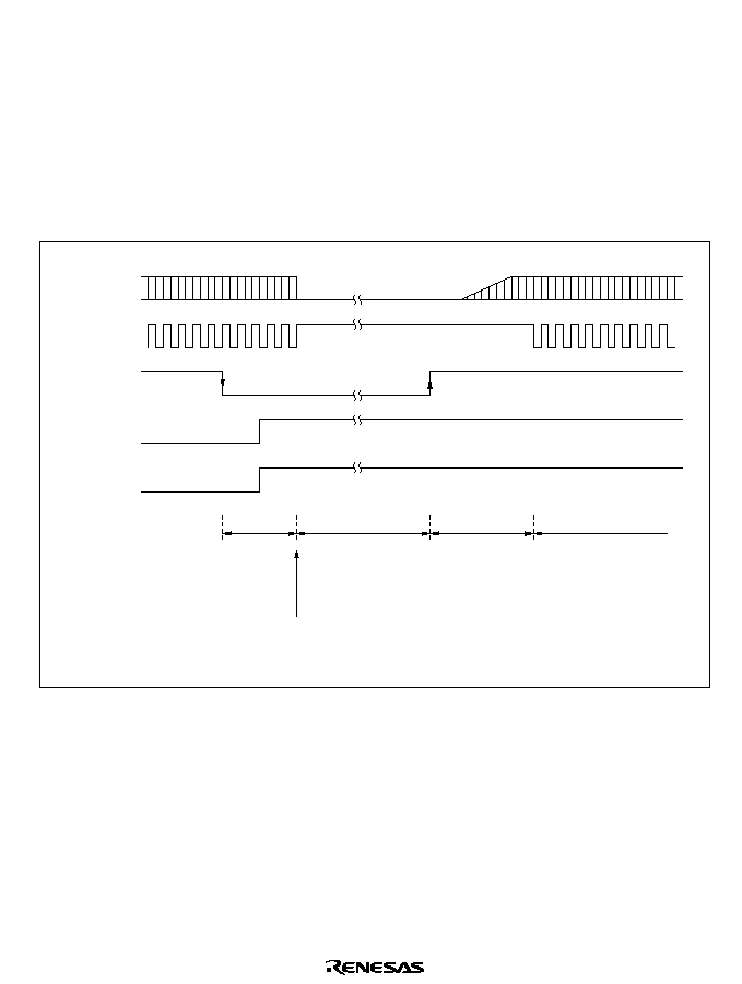
705
20.4.4
Sample Application of Software Standby Mode
Figure 20.1 shows an example in which software standby mode is entered at the fall of NMI and
exited at the rise of NMI.
With the NMI edge select bit (NMIEG) cleared to 0 in SYSCR (selecting the falling edge), an
NMI interrupt occurs. Next the NMIEG bit is set to 1 (selecting the rising edge) and the SSBY bit
is set to 1; then the SLEEP instruction is executed to enter software standby mode.
Software standby mode is exited at the next rising edge of the NMI signal.
NMI
NMIEG
SSBY
NMI interrupt
handler
NMIEG = 1
SSBY = 1
Software standby
mode (power-
down state)
Oscillator
settling time
(t
osc2
)
SLEEP
instruction
NMI exception
handling
Clock
oscillator
Figure 20.1 NMI Timing for Software Standby Mode (Example)
20.4.5
Note
The I/O ports retain their existing states in software standby mode. If a port is in the high output
state, its output current is not reduced.

706
20.5
Hardware Standby Mode
20.5.1
Transition to Hardware Standby Mode
Regardless of its current state, the chip enters hardware standby mode whenever the
STBY pin
goes low. Hardware standby mode reduces power consumption drastically by halting all functions
of the CPU, DMAC, DRAM interface, and on-chip supporting modules. All modules are reset
except the on-chip RAM. As long as the specified voltage is supplied, on-chip RAM data is
retained. I/O ports are placed in the high-impedance state.
Clear the RAME bit to 0 in SYSCR before
STBY goes low to retain on-chip RAM data.
The inputs at the mode pins (MD2 to MD0) should not be changed during hardware standby
mode.
Note : Do not select the hardware standby mode during the reset period following power-on.
20.5.2
Exit from Hardware Standby Mode
Hardware standby mode is exited by inputs at the
STBY and RES pins. While RES is low, when
STBY goes high, the clock oscillator starts running. RES should be held low long enough for the
clock oscillator to settle. When
RES goes high, reset exception handling begins, followed by a
transition to the program execution state.
20.5.3
Timing for Hardware Standby Mode
Figure 20.2 shows the timing relationships for hardware standby mode. To enter hardware standby
mode, first drive
RES low, then drive STBY low. To exit hardware standby mode, first drive
STBY high, wait for the clock to settle, then bring RES from low to high.
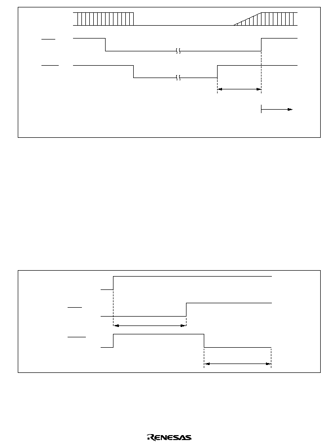
707
RES
STBY
Clock
oscillator
Oscillator
settling time
Reset
exception
handling
Figure 20.2 Hardware Standby Mode Timing
20.5.4 Timing for Hardware Standby Mode at Power-On
Figure 20.3 shows the timing relationships for entering hardware standby mode when the power is
turned on.
To make a transition to hardware standby mode when the power is turned on, hold the
RES pin
low for the stipulated time while keeping the
STBY pin high. After the reset is cleared, set the
STBY pin low.
For details on exiting hardware standby mode, see section 20.5.3, Timing for Hardware Standby
Mode.
RES
STBY
Power
supply
Reset period
Hardware standby
mode
Figure 20.3 Timing for Hardware Standby Mode at Power-On

708
20.6
Module Standby Function
20.6.1
Module Standby Timing
The module standby function can halt several of the on-chip supporting modules (SCI2, SCI1,
SCI0, the DMAC, 16-bit timer, 8-bit timer, DRAM interface, and A/D converter) independently in
the power-down state. This standby function is controlled by bits MSTPH2 to MSTPH0 in
MSTCRH and bits MSTPL7 to MSTPL0 in MSTCRL. When one of these bits is set to 1, the
corresponding on-chip supporting module is placed in standby and halts at the beginning of the
next bus cycle after the MSTCR write cycle.
20.6.2
Read/Write in Module Standby
When an on-chip supporting module is in module standby, read/write access to its registers is
disabled. Read access always results in H'FF data. Write access is ignored.
20.6.3
Usage Notes
When using the module standby function, note the following points.
DMAC: When setting a bit in MSTCR to 1 to place the DMAC in module standby, make sure that
the DMAC is not currently requesting the bus right. If the corresponding bit in MSTCR is set to 1
when a bus request is present, operation of the bus arbiter becomes ambiguous and a malfunction
may occur.
DRAM Interface: When the module standby function is used on the DRAM interface, set the
MSTCR bit to 1 while DRAM space is deselected.
On-Chip Supporting Module Interrupts: Before setting a module standby bit, first disable
interrupts by that module. When an on-chip supporting module is placed in standby by the module
standby function, its registers are initialized, including registers with interrupt request flags.
Pin States: Pins used by an on-chip supporting module lose their module functions when the
module is placed in module standby. What happens after that depends on the particular pin. For
details, see section 8, I/O Ports. Pins that change from the input to the output state require special
care. For example, if SCI1 is placed in module standby, the receive data pin loses its receive data
function and becomes a port pin. If its port DDR bit is set to 1, the pin becomes a data output pin,
and its output may collide with external SCI transmit data. Data collision should be prevented by
clearing the port DDR bit to 0 or taking other appropriate action.
Register Resetting: When an on-chip supporting module is halted by the module standby
function, all its registers are initialized. To restart the module, after its MSTCR bit is cleared to 0,
its registers must be set up again. It is not possible to write to the registers while the MSTCR bit is
set to 1.
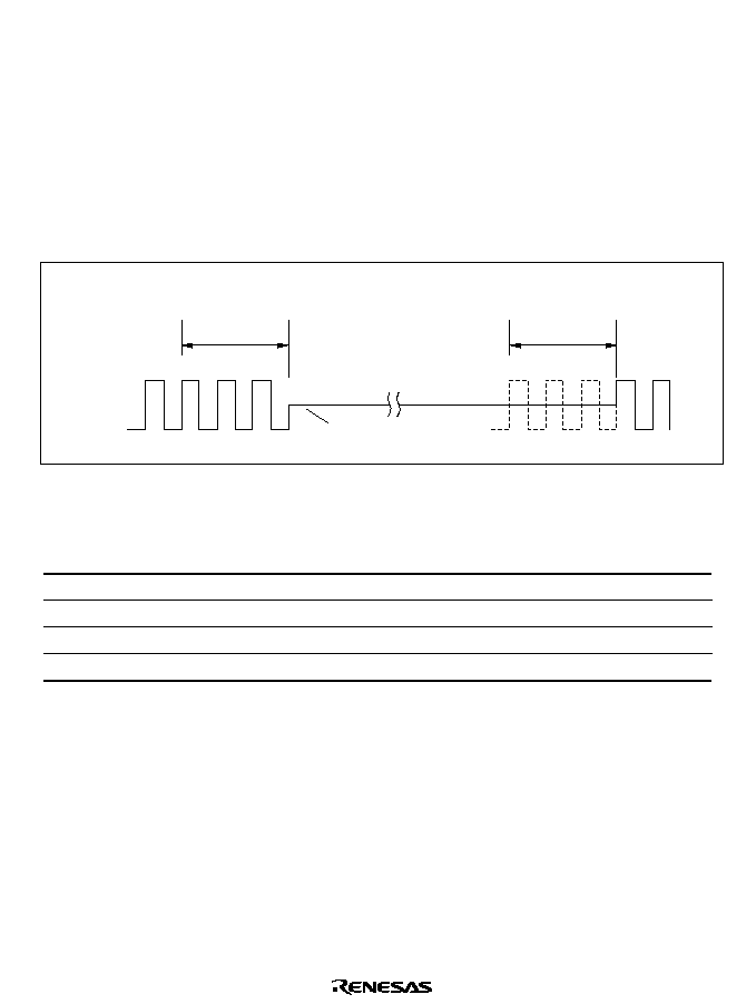
709
MSTCR Access from DMAC Disabled: To prevent malfunctions, MSTCR can only be accessed
from the CPU. It can be read by the DMAC, but it cannot be written by the DMAC.
20.7
System Clock Output Disabling Function
Output of the system clock (
) can be controlled by the PSTOP bit in MSTCRH. When the
PSTOP bit is set to 1, output of the system clock halts and the
pin is placed in the high-
impedance state. Figure 20.4 shows the timing of the stopping and starting of system clock output.
When the PSTOP bit is cleared to 0, output of the system clock is enabled. Table 20.4 indicates
the state of the
pin in various operating states.
T1
T2
(PSTOP = 1)
T3
T1
T2
(PSTOP = 0)
MSTCRH write cycle
MSTCRH write cycle
High impedance
pin
T3
Figure 20.4 Starting and Stopping of System Clock Output
Table 20.4
Pin State in Various Operating States
Operating State
PSTOP = 0
PSTOP = 1
Hardware standby
High impedance
High impedance
Software standby
Always high
High impedance
Sleep mode
System clock output
High impedance
Normal operation
System clock output
High impedance

710

711
Section 21 Electrical Characteristics
21.1
Electrical Characteristics of H8/3069F-ZTAT
21.1.1
Absolute Maximum Ratings
Table 21.1 lists the absolute maximum ratings.
Table 21.1
Absolute Maximum Ratings
Item
Symbol
Value
Unit
Power supply voltage
V
CC
*
1
�0.3 to +7.0
V
Input voltage (FWE)
*
2
V
in
�0.3 to V
CC
+0.3
V
Input voltage (except for port 7)
*
2
V
in
�0.3 to V
CC
+0.3
V
Input voltage (port 7)
V
in
�0.3 to AV
CC
+0.3
V
Reference voltage
V
REF
�0.3 to AV
CC
+0.3
V
Analog power supply voltage
AV
CC
�0.3 to +7.0
V
Analog input voltage
V
AN
�0.3 to AV
CC
+0.3
V
Operating temperature
T
opr
Regular specifications: �20 to +75
*
3
Wide-range specifications: �40 to +85
*
3
�
C
Storage temperature
T
stg
�55 to +125
�
C
Caution: Permanent damage to the chip may result if absolute maximum ratings are exceeded.
Notes:
*
1 Do not apply the power supply voltage to the V
CL
pin. Connect an external capacitor
between this pin and GND.
*
2 12 V must not be applied to any pin, as this may cause permanent damage to the
device.
*
3 The operating temperature range for flash memory programming/erasing is T
a
= 0 to
+75
�
C (Regular specifications) T
a
= 0 to +85
�
C (Wide-range specifications).

712
21.1.2
DC Characteristics
Table 21.2 lists the DC characteristics. Table 21.3 lists the permissible output currents.
Table 21.2
DC Characteristics
Conditions: V
CC
= AV
CC
= 5.0 V
�
10%, V
REF
= 4.5 V to AV
CC
*
1
, V
SS
= AV
SS
= 0 V*
1
,
T
a
=�20
�
C to +75
�
C (Regular specifications),
T
a
= �40
�
C to +85
�
C (Wide-range specifications)
[Programming/erasing conditions: T
a
= 0
�
C to +75
�
C (Regular specifications),
T
a
= 0
�
C to +85
�
C (Wide-range specifications)]
Item
Symbol
Min
Typ
Max
Unit
Test Conditions
Schmitt trigger
input voltages
Port A,
P8
0
to P8
2
V
T
�
V
T
+
V
T
+
� V
T
�
1.0
--
0.4
--
--
--
--
V
CC
�
0.7
--
V
V
V
Input high
voltage
STBY
,
RES
,
NMI, MD
2
to
MD
0
, FWE
V
IH
V
CC
� 0.7
--
V
CC
+ 0.3
V
EXTAL
V
CC
�
0.7
--
V
CC
+ 0.3
V
Port 7
2.0
--
AV
CC
+ 0.3 V
Ports 1 to 6,
P8
3
, P8
4
, P9
0
to P9
5
, port B
2.0
--
V
CC
+ 0.3
V
Input low
voltage
STBY
,
RES
,
FWE, MD
2
to
MD
0
V
IL
�0.3
--
0.5
V
NMI, EXTAL,
ports 1 to 7,
P8
3
, P8
4
, P9
0
to P9
5
, port B
�0.3
--
0.8
V
Output high
voltage
All output pins
V
OH
V
CC
� 0.5
3.5
--
--
--
--
V
V
I
OH
= �200
�
A
I
OH
= �1 mA
Output low
voltage
All output pins
V
OL
--
--
0.4
V
I
OL
= 1.6 mA
Ports 1, 2,
and 5
--
--
1.0
V
I
OL
= 10 mA
Input leakage
current
STBY
,
RES
,
NMI, FWE,
MD
2
to MD
0
|I
in
|
--
--
1.0
�
A
V
in
= 0.5 V to
V
CC
� 0.5 V
Port 7
--
--
1.0
�
A
V
in
= 0.5 V to
AV
CC
� 0.5 V

713
Item
Symbol
Min
Typ
Max
Unit
Test Conditions
Three-state
leakage
current
Ports 1 to 6
Ports 8 to B
|I
TSI
|
--
--
1.0
�
A
V
in
= 0.5 V to
V
CC
� 0.5 V
Input pull-up
MOS current
Ports 2, 4,
and 5
�I
p
50
--
360
�
A
V
in
= 0 V
Input
capacitance
FWE
C
in
--
--
80
pF
V
in
= 0 V
f = f
min
,
NMI
--
--
50
pF
T
a
= 25
�
C
All input pins
except NMI
--
--
15
pF
Current
dissipation
*
2
Normal
operation
I
CC
*
3
--
24
(5.0 V)
36
mA
f = 25 MHz
Sleep mode
--
20
(5.0 V)
33
mA
f = 25 MHz
Module
standby mode
--
15
(5.0 V)
25
mA
f = 25 MHz
Standby mode
--
25
(5.0 V)
90
�
A
T
a
50
�
C
--
--
120
�
A
50
�
C
<
T
a
Flash memory
programming/
erasing
*
4
--
34
(5.0 V)
46
mA
f = 25 MHz
Analog power
supply current
During A/D
conversion
AI
CC
--
0.9
1.5
mA
During A/D
and D/A
conversion
--
0.9
1.5
mA
Idle
--
0.05
(5.0 V)
5
�
A
T
a
50
�
C
at DASTE = 0
--
--
15
�
A
50
�
C
<
T
a
at DASTE = 0

714
Item
Symbol
Min
Typ
Max
Unit
Test Conditions
Reference
current
During A/D
conversion
AI
CC
--
0.45
0.8
mA
During A/D
and D/A
conversion
--
1.8
3.0
mA
Idle
--
0.05
5.0
�
A
DASTE = 0
RAM standby voltage
V
RAM
3.0
--
--
V
Notes:
*
1 If the A/D converter is not used, do not leave the AV
CC
, V
REF
, and AV
SS
pins open.
Connect AV
CC
and V
REF
to V
CC
, and connect AV
SS
to V
SS
.
*
2 Current dissipation values are for V
IH
min = V
CC
� 0.5 V and V
IL
max = 0.5 V with all
output pins unloaded and the on-chip MOS pull-up transistors in the off state.
*
3 I
CC
max. (normal operation)= 15 (mA) + 0.15 (mA/(MHz
�
V))
�
V
CC
�
f
I
CC
max. (sleep mode)
= 15 (mA) + 0.13 (mA/(MHz
�
V))
�
V
CC
�
f
I
CC
max. (sleep mode + module standby mode)
= 15 (mA) + 0.07 (mA/(MHz
�
V))
�
V
CC
�
f
The Typ values for power consumption are reference values.
*
4 Sum of current dissipation in normal operation and current dissipation in program/erase
operations.
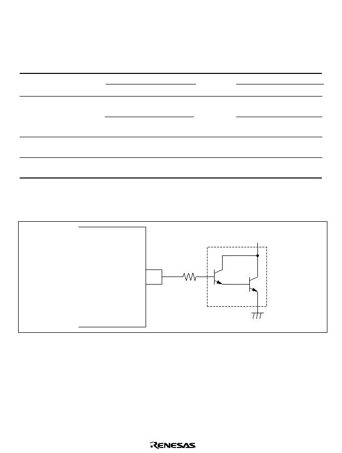
715
Table 21.3
Permissible Output Currents
Conditions: V
CC
= AV
CC
= 5.0 V
�
10%, V
REF
= 4.5 V to AV
CC
, V
SS
= AV
SS
= 0 V,
T
a
= �20
�
C to +75
�
C (Regular specifications),
T
a
= �40
�
C to +85
�
C (Wide-range specifications)
Item
Symbol
Min
Typ
Max
Unit
Permissible output
low current (per pin)
Ports 1, 2, and 5
Other output pins
I
OL
--
--
--
--
10
2.0
mA
mA
Permissible output
low current (total)
Total of 20 pins in
Ports 1, 2, and 5
I
OL
--
--
80
mA
Total of all output pins,
including the above
--
--
120
mA
Permissible output
high current (per pin)
All output pins
| �I
OH
|
--
--
2.0
mA
Permissible output
high current (total)
Total of all output pins
| �
I
OH
|
--
--
40
mA
Notes: 1. To protect chip reliability, do not exceed the output current values in table 21.3.
2. When directly driving a darlington pair or LED, always insert a current-limiting resistor in
the output line, as shown in figures 21.1 and 21.2.
H8/3069F-ZTAT
Port
2 k
Darlington pair
Figure 21.1 Darlington Pair Drive Circuit (Example)
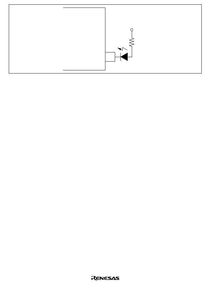
716
H8/3069F-ZTAT
Ports 1, 2, 5
LED
600
Figure 21.2 Sample LED Circuit

717
21.1.3
AC Characteristics
Clock timing parameters are listed in table 21.4, control signal timing parameters in table 21.5,
and bus timing parameters in table 21.6. Timing parameters of the on-chip supporting modules are
listed in table 21.7.
Table 21.4
Clock Timing
Condition:
T
a
= �20
�
C to +75
�
C (Regular specifications),
T
a
= �40
�
C to +85
�
C (Wide-range specifications)
V
CC
= AV
CC
= 5.0 V
�
10%, V
REF
= 4.5 to AV
CC
, V
SS
= AV
SS
= 0 V, fmax = 25 MHz
Item
Symbol
Min
Max
Unit
Test
Conditions
Clock cycle time
Clock pulse low width
t
cyc
t
CL
40
10
100
--
ns
ns
Figure 21.7
Clock pulse high width
t
CH
10
--
ns
Clock rise time
t
Cr
--
10
ns
Clock fall time
t
Cf
--
10
ns
Clock oscillator settling
time at reset
t
OSC1
20
--
ms
Figure 21.4
Clock oscillator settling
time in software standby
t
OSC2
7
--
ms
Figure 20.1
Table 21.5
Control Signal Timing
-- Preliminary --
Conditions: T
a
= �20
�
C to +75
�
C (Regular specifications),
T
a
= �40
�
C to +85
�
C (Wide-range specifications)
V
CC
= AV
CC
= 5.0 V
�
10%, V
REF
= 4.5 to AV
CC
, V
SS
= AV
SS
= 0 V, fmax = 25 MHz
Item
Symbol
Min
Max
Unit
Test
Conditions
RES
setup time
t
RESS
150
--
ns
Figure 21.5
RES
pulse width
t
RESW
20
--
t
cyc
Mode programming setup
time
t
MDS
200
--
ns
NMI,
IRQ
setup time
t
NMIS
150
--
ns
Figure 21.6
NMI,
IRQ
hold time
t
NMIH
10
--
ns
NMI,
IRQ
pulse width
t
NMIW
200
--
ns

718
Table 21.6
Bus Timing
Conditions: T
a
= �20
�
C to +75
�
C (Regular specifications),
T
a
= �40
�
C to +85
�
C (Wide-range specifications)
V
CC
= AV
CC
= 5.0 V
�
10%, V
REF
= 4.5 to AV
CC
, V
SS
= AV
SS
= 0 V, fmax = 25 MHz
Item
Symbol
Min
Max
Unit
Test
Conditions
Address delay time
t
AD
--
25
ns
Figure 21.7,
Address hold time
t
AH
0.5 t
cyc
� 20
--
ns
Figure 21.8,
Read strobe delay time
t
RSD
--
25
ns
Figure 21.10,
Address strobe delay
time
t
ASD
--
25
ns
Figure 21.11,
Figure 21.13
Write strobe delay time
t
WSD
--
25
ns
Strobe delay time
t
SD
--
25
ns
Write strobe pulse
width 1
t
WSW1
1.0 t
cyc
� 25
--
ns
Write strobe pulse
width 2
t
WSW2
1.5 t
cyc
� 25
--
ns
Address setup time 1
t
AS1
0.5 t
cyc
� 20
--
ns
Address setup time 2
t
AS2
1.0 t
cyc
� 20
--
ns
Read data setup time
t
RDS
25
--
ns
Read data hold time
t
RDH
0
--
ns
Write data delay time
t
WDD
--
35
ns
Write data setup time 1
t
WDS1
1.0 t
cyc
� 30
--
ns
Write data setup time 2
t
WDS2
2.0 t
cyc
� 30
--
ns
Write data hold time
t
WDH
0.5 t
cyc
� 15
--
ns

719
Item
Symbol
Min
Max
Unit
Test
Conditions
Read data access
time 1
t
ACC1
--
2.0 t
cyc
� 45
ns
Figure 21.7,
Figure 21.8,
Read data access
time 2
t
ACC2
--
3.0 t
cyc
� 45
ns
Figure 21.10,
Figure 21.11
Read data access
time 3
t
ACC3
--
1.5 t
cyc
� 45
ns
Read data access
time 4
t
ACC4
--
2.5 t
cyc
� 45
ns
Precharge time 1
t
PCH1
1.0 t
cyc
� 20
--
ns
Precharge time 2
t
PCH2
0.5 t
cyc
� 20
--
ns
Wait setup time
t
WTS
25
--
ns
Figure 21.9
Wait hold time
t
WTH
5
--
ns
Bus request setup time
t
BRQS
25
--
ns
Figure 21.12
Bus acknowledge delay
time 1
t
BACD1
--
30
ns
Bus acknowledge delay
time 2
t
BACD2
--
30
ns
Bus-floating time
t
BZD
--
30
ns
RAS
precharge time
t
RP
1.5 t
cyc
� 25
--
ns
Figure 21.13,
CAS
precharge time
t
CP
0.5 t
cyc
� 15
--
ns
Figure 21.14
Low address hold time
t
RAH
0.5 t
cyc
� 15
--
ns
RAS
delay time 1
t
RAD1
--
25
ns
RAS
delay time 2
t
RAD2
--
30
ns
CAS
delay time 1
t
CASD1
--
25
ns
CAS
delay time 2
t
CASD2
--
25
ns
WE
delay time
t
WCD
--
25
ns

720
Item
Symbol
Min
Max
Unit
Test
Conditions
CAS
pulse width 1
t
CAS1
1.5 t
cyc
� 20
--
ns
Figure 21.13
to
CAS
pulse width 2
t
CAS2
1.0 t
cyc
� 20
--
ns
Figure 21.15
CAS
pulse width 3
t
CAS3
1.0 t
cyc
� 20
--
ns
RAS
access time
t
RAC
--
2.5 t
cyc
� 40
ns
Address access time
t
AA
--
2.0 t
cyc
� 50
ns
CAS
access time
t
CAC
--
1.5 t
cyc
� 50
ns
WE
setup time
t
WCS
0.5 t
cyc
� 20
--
ns
WE
hold time
t
WCH
0.5 t
cyc
� 15
--
ns
Write data setup time
t
WDS
0.5 t
cyc
� 20
--
ns
WE
write data hold time
t
WDH
0.5 t
cyc
� 15
--
ns
CAS
setup time 1
t
CSR1
0.5 t
cyc
� 20
--
ns
CAS
setup time 2
t
CSR2
0.5 t
cyc
� 15
--
ns
CAS
hold time
t
CHR
0.5 t
cyc
� 15
--
ns
RAS
pulse width
t
RAS
1.5 t
cyc
� 15
--
ns
Note:
In order to secure the address hold time relative to the rise of the
RD
strobe, address
update mode 2 should be used. For details see section 6.3.5, Address Output Method.

721
Table 21.7
Timing of On-Chip Supporting Modules
Conditions: T
a
= �20
�
C to +75
�
C (Regular specifications),
T
a
= �40
�
C to +85
�
C (Wide-range specifications)
V
CC
= AV
CC
= 5.0 V
�
10%, V
REF
= 4.5 to AV
CC
, V
SS
= AV
SS
= 0 V, fmax = 25 MHz
Module Item
Symbol
Min
Max
Unit
Test
Conditions
Ports
and
TPC
Output data
delay time
Input data setup
time
t
PWD
t
PRS
--
50
50
--
ns
ns
Figure 21.16
Input data hold
time
t
PRH
50
--
ns
16-bit
timer
Timer output
delay time
t
TOCD
--
50
ns
Figure 21.17
Timer input
setup time
t
TICS
50
--
ns
Timer clock
input setup time
t
TCKS
50
--
ns
Figure 21.18
Timer
clock
Single
edge
t
TCKWH
1.5
--
t
cyc
pulse
width
Both
edges
t
TCKWL
2.5
--
t
cyc
8-bit
timer
Timer output
delay time
t
TOCD
--
50
ns
Figure 21.17
Timer input
setup time
t
TICS
50
--
ns
Timer clock
input setup time
t
TCKS
50
--
ns
Figure 21.18
Timer
clock
Single
edge
t
TCKWH
1.5
--
t
cyc
pulse
width
Both
edges
t
TCKWL
2.5
--
t
cyc
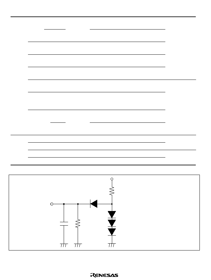
722
Module Item
Symbol
Min
Max
Unit
Test
Conditions
SCI
Input
clock
Asyn-
chronous
t
Scyc
4
--
t
cyc
Figure 21.19
cycle
Syn-
chronous
6
--
t
cyc
Input clock rise
time
t
SCKr
1.5
--
t
cyc
Input clock fall
time
t
SCKf
1.5
--
t
cyc
Input clock
pulse width
t
SCKW
0.4
0.6
t
Scyc
Transmit data
delay time
t
TXD
--
100
ns
Figure 21.20
Receive data
setup time
(synchronous)
t
RXS
100
--
ns
Receive
data hold
Clock
input
t
RXH
100
--
ns
time (syn-
chronous)
Clock
output
0
--
ns
DMAC
TEND
delay time 1 t
TED1
--
50
ns
Figure 21.21,
TEND
delay time 2 t
TED2
--
50
ns
Figure 21.22
DREQ
setup time
t
DRQS
25
--
ns
Figure 21.23
DREQ
hold time
t
DRQH
10
--
ns
C
R
H
R
L
H8/3069F-ZTAT
output pin
C = 90 pF:
A
19
to A
0
, D
15
to D
8
Ports 4, 6, 8
C = 30 pF: Ports 9, A, B
Input/output timing measurement
levels
� Low: 0.8 V
� High: 2.0 V
R = 2.4 k
R = 12 k
L
H
Figure 21.3 Output Load Circuit

723
21.1.4
A/D Conversion Characteristics
Table 21.8 lists the A/D conversion characteristics.
Table 21.8
A/D Conversion Characteristics
Conditions: T
a
= �20
�
C to +75
�
C (Regular specifications),
T
a
= �40
�
C to +85
�
C (Wide-range specifications)
V
CC
= AV
CC
= 5.0 V
�
10%, V
REF
= 4.5 to AV
CC
, V
SS
= AV
SS
= 0 V, fmax = 25 MHz
Item
Min
Typ
Max
Unit
Conver-
sion time:
134 states
Resolution
Conversion time (single
mode)
10
--
10
--
10
134
bits
t
cyc
Analog input capacitance
--
--
20
pF
Permissible
signal-source
13 MHz
--
--
10
k
impedance
> 13 MHz
--
--
5
k
Nonlinearity error
--
--
�
3.5
LSB
Offset error
--
--
�
3.5
LSB
Full-scale error
--
--
�
3.5
LSB
Quantization error
--
--
�
0.5
LSB
Absolute accuracy
--
--
�
4.0
LSB
Item
Min
Typ
Max
Unit
Conver-
sion time:
70 states
Resolution
Conversion time (single
mode)
10
--
10
--
10
70
bits
t
cyc
Analog input capacitance
--
--
20
pF
Permissible
signal-source
13 MHz
--
--
5
k
impedance
> 13 MHz
--
--
3
k
Nonlinearity error
--
--
�
7.5
LSB
Offset error
--
--
�
7.5
LSB
Full-scale error
--
--
�
7.5
LSB
Quantization error
--
--
�
0.5
LSB
Absolute accuracy
--
--
�
8.0
LSB

724
21.1.5
D/A Conversion Characteristics
Table 21.9 lists the D/A conversion characteristics.
Table 21.9
D/A Conversion Characteristics
Conditions:
T
a
= �20
�
C to +75
�
C (Regular specifications),
T
a
= �40
�
C to +85
�
C (Wide-range specifications)
V
CC
= AV
CC
= 5.0 V
�
10%, V
REF
= 4.5 to AV
CC
, V
SS
= AV
SS
= 0 V, fmax = 25 MHz
Item
Min
Typ
Max
Unit
Test Conditions
Resolution
8
8
8
bits
Conversion time
(centering time)
--
--
10
�
s
20 pF capacitive
load
Absolute accuracy
--
�
1.5
�
2.0
LSB
2 M
resistive
load
--
--
�
1.5
LSB
4 M
resistive
load

725
21.1.6
Flash Memory Characteristics
Table 21.10 shows the flash memory characteristics.
Table 21.10 Flash Memory Characteristics
Conditions: V
CC
= AV
CC
= 4.5 to 5.5 V, V
SS
= AV
SS
= 0 V,
T
a
= 0
�
C to +75 (operating temperature range for programming/erasing :
Regular specifications)
T
a
= 0
�
C to +85 (operating temperature range for programming/erasing :
Wide-range specifications)
Item
Symbol
Min
Typ
Max
Unit
Notes
Programming time
*
1,
*
2,
*
4
t
P
--
3
30
ms/
128 bytes
Erase time
*
1,
*
2,
*
4
t
E
--
80
800
ms/4k
blocks
--
500
5000
ms/32k
blocks
--
1000
10000 ms/64k
blocks
Programming time (total)
*
1,
*
2,
*
4
t
P
--
10
30
s/512k
bytes
T
a
= 25
�
C,
all "0"
Erase time (total)
*
1,
*
2,
*
4
t
E
--
10
30
s/512k
bytes
T
a
= 25
�
C
Programming and erase time (total)
*
1,
*
2,
*
4
t
PE
--
20
60
s/512k
bytes
T
a
= 25
�
C
Reprogramming count
N
WEC
100
*
3
--
--
times
Data retention time
*
4
t
DRP
10
--
--
year
Notes:
*
1 Programming and erase time depend on the data size.
*
2 Programming and erase time excluded the data transfer time.
*
3 It is the number of times of min. which guarantees all the characteristics after
reprogramming. (A guarantee is the range of a 1-min. value.)
*
4 It is the characteristic when reprogramming is performed by specification within the
limits including a min. value.
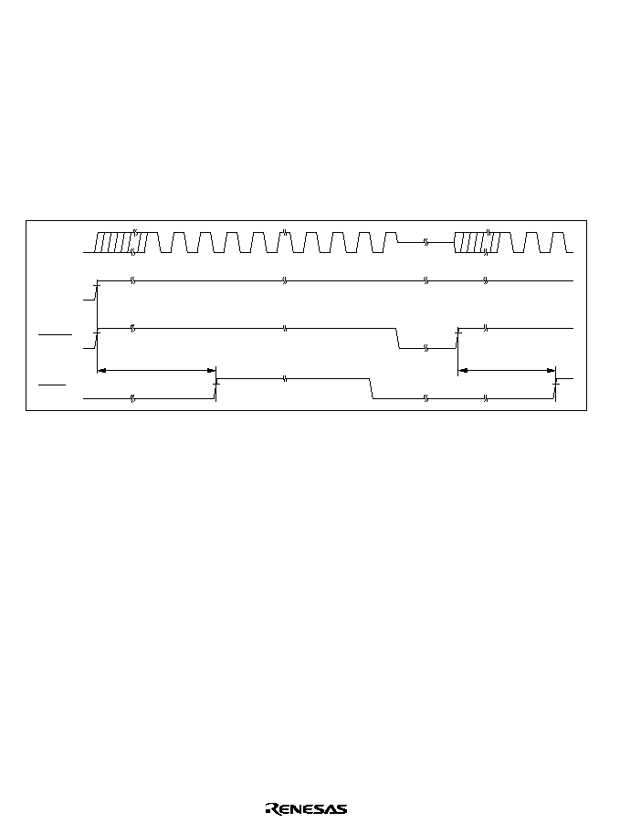
726
21.2
Operational Timing
This section shows timing diagrams.
21.2.1
Clock Timing
Clock timing is shown as follows:
�
Oscillator settling timing
Figure 21.4 shows the oscillator settling timing.
V
CC
STBY
RES
t
OSC1
t
OSC1
Figure 21.4 Oscillator Settling Timing
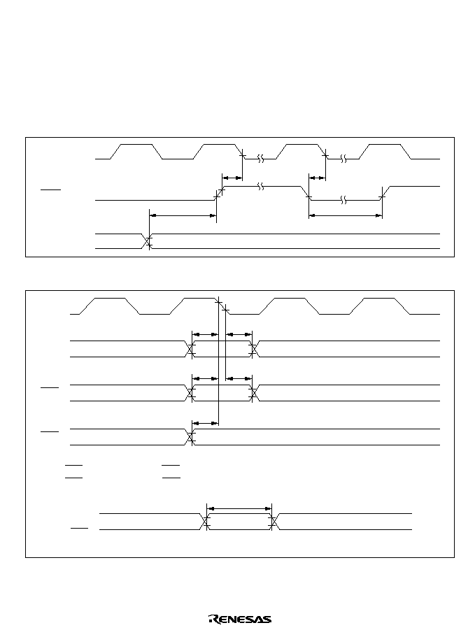
727
21.2.2
Control Signal Timing
Control signal timing is shown as follows:
�
Reset input timing
Figure 21.5 shows the reset input timing.
�
Interrupt input timing
Figure 21.6 shows the interrupt input timing for NMI and
IRQ
5
to
IRQ
0
.
t
RESS
t
RESS
t
RESW
t
MDS
RES
MD
2
to MD
0
FWE
Figure 21.5 Reset Input Timing
NMI
IRQ
IRQ
E
L
t
NMIS
t
NMIH
t
NMIS
t
NMIH
t
NMIS
t
NMIW
NMI
IRQ
j
IRQ : Edge-sensitive IRQ
: Level-sensitive IRQ (i = 0 to 5)
E
L
i
i
IRQ
(j = 0 to 5)
Figure 21.6 Interrupt Input Timing

728
21.2.3
Bus Timing
Bus timing is shown as follows:
�
Basic bus cycle: two-state access
Figure 21.7 shows the timing of the external two-state access cycle.
�
Basic bus cycle: three-state access
Figure 21.8 shows the timing of the external three-state access cycle.
�
Basic bus cycle: three-state access with one wait state
Figure 21.9 shows the timing of the external three-state access cycle with one wait state
inserted.
�
Burst ROM access timing/burst cycle: two-state access
Figure 21.10 shows the timing of the two-state burst cycle.
�
Burst ROM access timing/burst cycle: three-state access
Figure 21.11 shows the timing of the three-state burst cycle.
�
Burst release mode timing
Figure 21.12 shows the timing in bus release mode.
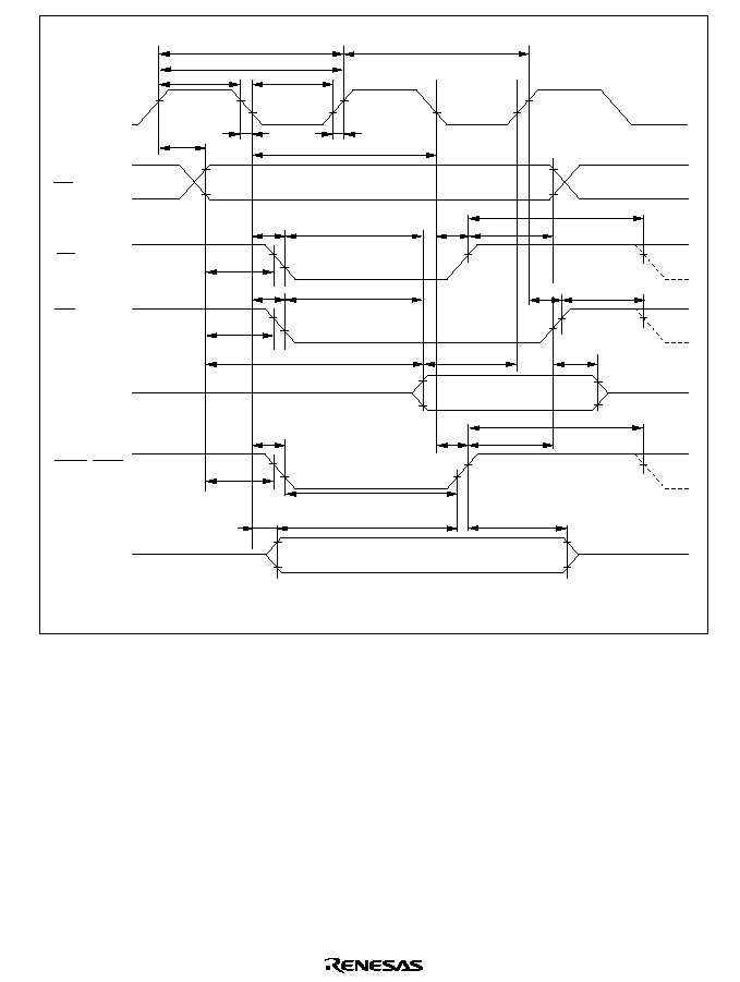
729
T
1
T
2
t
CH
t
AD
t
CL
t
Cr
t
Cf
t
ASD
t
ACC3
t
AS1
t
cyc
t
cyc
t
SD
t
RDS
t
AH
t
PCH1
t
PCH2
t
RDH
*
t
PCH1
t
SD
t
AH
t
ASD
t
ACC3
t
AS1
t
ACC1
t
ASD
t
AS1
t
WSW1
t
WDS1
t
WDH
t
WDD
A
23
to A
0
,
CS
n
AS
RD
(read)
D
15
to D
0
(read)
HWR, LWR
(write)
D
15
to D
0
(write)
Note:
*
Specification from the earliest negation timing of A
23
to A
0
,
CS
n
, and
RD
.
t
RSD
Figure 21.7 Basic Bus Cycle: two State Access
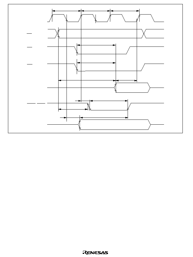
730
T
1
T
2
T
3
t
ACC4
t
ACC4
t
AS2
t
WDS2
t
WSW2
t
WSD
t
WDD
t
ACC2
t
RDS
A
23
to A
0
,
CS
n
AS
RD
(read)
D
15
to D
0
(read)
HWR, LWR
(write)
D
15
to D
0
(write)
Figure 21.8 Basic Bus Cycle: three State Access
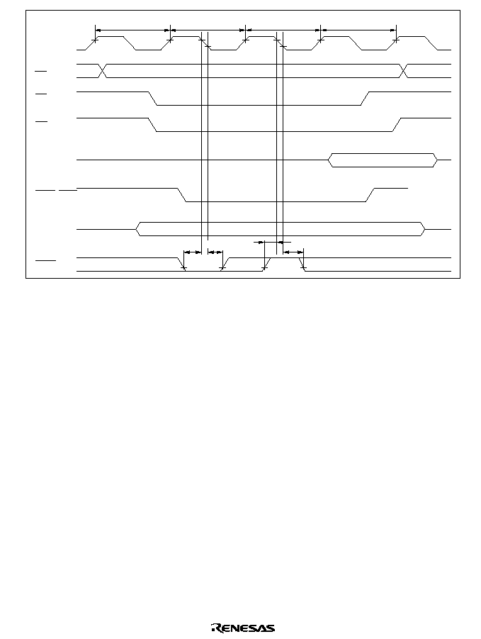
731
T
1
T
2
T
W
T
3
t
WTS
t
WTS
t
WTH
AS
RD (read)
D
15
to D
0
(read)
HWR, LWR
(write)
D
15
to D
0
(write)
WAIT
t
WTH
A
23
to A
0
,
CS
n
Figure 21.9 Basic Bus Cycle: three State Access with One Wait State
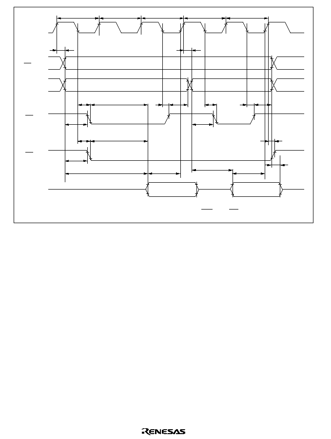
732
t
AD
t
ASD
t
AS1
t
ACC4
t
RDS
t
RDS
T
3
T
1
T
2
T
2
T
1
t
ASD
t
SD
t
AH
t
AS1
t
AH
t
SD
t
ASD
t
AS1
t
ACC4
t
ACC2
t
RSD
t
RDH
*
t
ACC1
t
AD
A
23
to A
3
CSn
A
2
to A
0
AS
RD
D
15
to D
0
Note:
*
Specification from the earliest negation timing of A
23
to A
0
, CSn, and RD.
Figure 21.10 Burst ROM Access Timing: two State Access
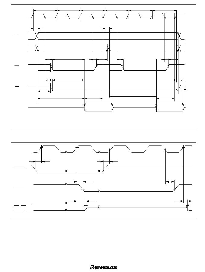
733
t
AD
t
ASD
t
AS1
t
ACC4
t
RDS
t
RDS
T
3
T
1
T
2
T
3
T
2
T
1
t
ASD
t
SD
t
AH
t
AS1
t
AH
t
SD
t
ASD
t
AS1
t
ACC4
t
ACC2
t
RSD
t
RDH
*
t
ACC2
t
AD
A
23
to A
3
CSn
A
2
to A
0
AS
RD
D
15
to D
0
Note:
*
Specification from the earliest negation timing of A
23
to A
0
,
CS
n, and
RD
.
Figure 21.11 Burst ROM Access Timing: three State Access
BREQ
BACK
A
23
to A
0
,
AS, RD,
HWR, LWR
t
BRQS
t
BRQS
t
BACD1
t
BZD
t
BACD2
t
BZD
Figure 21.12 Bus-Release Mode Timing

734
21.2.4
DRAM Interface Bus Timing
DRAM interface bus timing is shown as follows:
�
DRAM bus timing: read and write access
Figure 21.13 shows the timing of the read and write access.
�
DRAM bus timing: CAS before RAS refresh
Figure 21.14 shows the timing of the CAS before RAS refresh.
�
DRAM bus timing: self-refresh
Figure 21.15 shows the timing of the self-refresh.
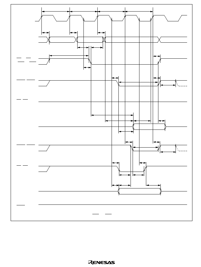
735
T
p
t
AD
T
r
T
C1
T
C2
t
RP
t
AD
t
AS1
t
RAD1
t
RAD2
t
CASD2
t
CP
t
ASD
t
CAS1
t
RDH
*
t
CASD2
t
CAS2
t
CP
t
CASD1
t
CAC
t
RDS
t
RAC
t
AA
t
RAH
t
AD
t
WCD
t
WCH
t
WCS
t
WDD
t
WDS
t
WDH
t
ASD
A
23
to A
0
CS
5
to CS
2
(RAS
5
to RAS
2
)
UCAS, LCAS
(read)
RD (WE)
(read)
High
High
UCAS, LCAS
(write)
RD (WE)
(write)
D
15
to D
0
(read)
D
15
to D
0
(write)
RFSH
Note:
*
Specification from the earliest negation timing of RAS and CAS.
Figure 21.13 DRAM Bus Timing (Read/Write)
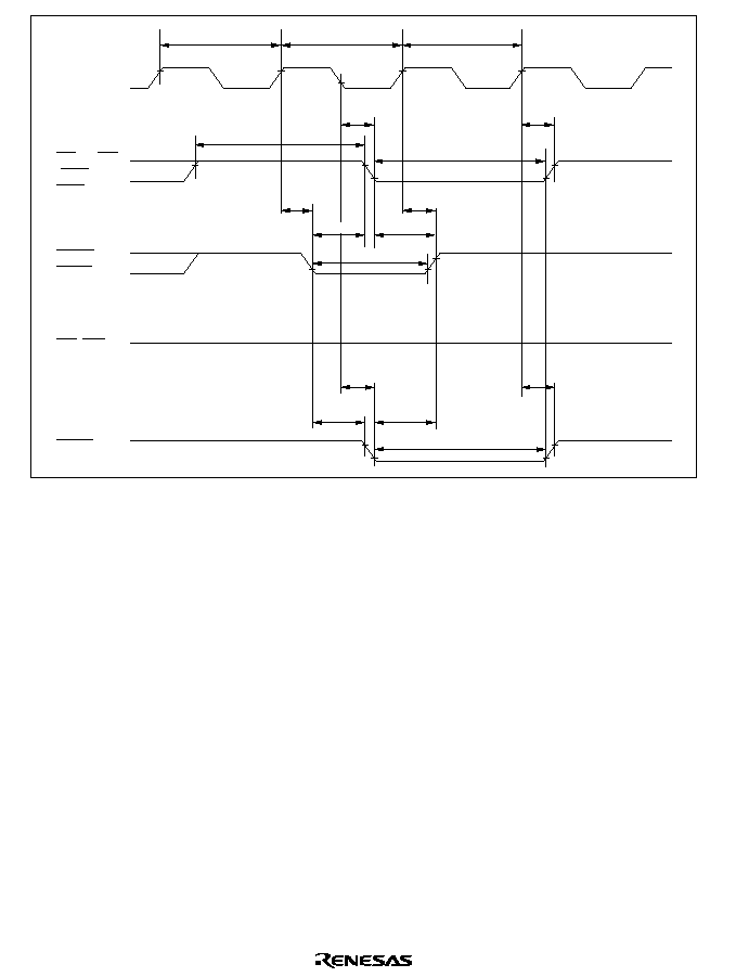
736
TR
p
TR
1
TR
2
t
RP
t
RAD1
t
CASD1
t
CASD2
t
RAD2
t
RAS
CS
5
to CS
2
(RAS
5
to
RAS
2
)
UCAS,
LCAS
RD (WE)
(high)
RFSH
t
CSR1
t
RAD1
t
CSR1
t
CHR
t
RAS
t
RAD2
t
CHR
t
CAS3
Figure 21.14 DRAM Bus Timing (CAS Before RAS Refresh)
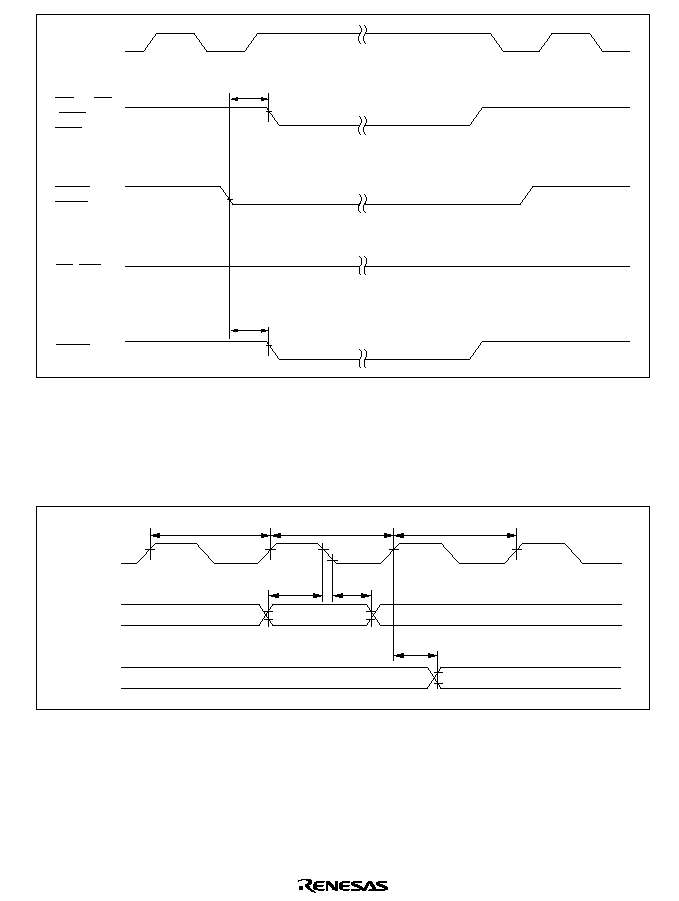
737
t
CSR2
t
CSR2
CS
5
to CS
2
(RAS
5
to
RAS
2
)
UCAS,
LCAS
RD (WE)
(high)
RFSH
Figure 21.15 DRAM Bus Timing (Self-Refresh)
21.2.5
TPC and I/O Port Timing
Figure 21.16 shows the TPC and I/O port input/output timing.
T
1
T
2
T
3
Port 1 to
B (read)
Port 1 to
6, 8 to B
(write)
t
PRS
t
PRH
t
PWD
Figure 21.16 TPC and I/O Port Input/Output Timing
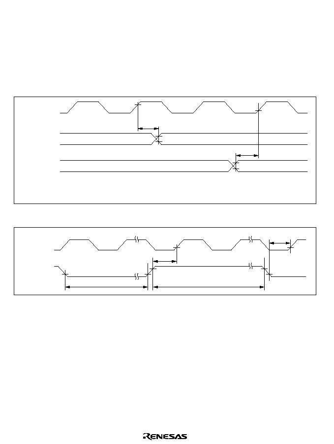
738
21.2.6
Timer Input/Output Timing
16-bit timer and 8-bit timer timing is shown below.
�
Timer input/output timing
Figure 21.17 shows the timer input/output timing.
�
Timer external clock input timing
Figure 21.18 shows the timer external clock input timing.
Output
compare
*
1
Input
capture
*
2
t
TOCD
t
TICS
Notes:
*
1 TIOCA0 to TIOCA2, TIOCB0 to TIOCB2, TMO0, TMO2, TMIO1, TMIO3
*
2 TIOCA0 to TIOCA2, TIOCB0 to TIOCB2, TMIO1, TMIO3
Figure 21.17 Timer Input/Output Timing
t
TCKS
t
TCKS
t
TCKWH
t
TCKWL
TCLKA to
TCLKD
Figure 21.18 Timer External Clock Input Timing
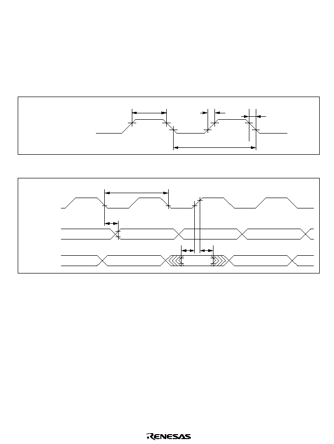
739
21.2.7
SCI Input/Output Timing
SCI timing is shown as follows:
�
SCI input clock timing
Figure 21.19 shows the SCI input clock timing.
�
SCI input/output timing (synchronous mode)
Figure 21.20 shows the SCI input/output timing in synchronous mode.
SCK
0
to SCK
2
t
SCKW
t
Scyc
t
SCKr
t
SCKf
Figure 21.19 SCI Input Clock Timing
t
Scyc
t
TXD
t
RXS
t
RXH
SCK
0
,
SCK
1
TxD
0
to TxD
2
(transmit
data)
RxD
0
to RxD
2
(receive
data)
Figure 21.20 SCI Input/Output Timing in Synchronous Mode
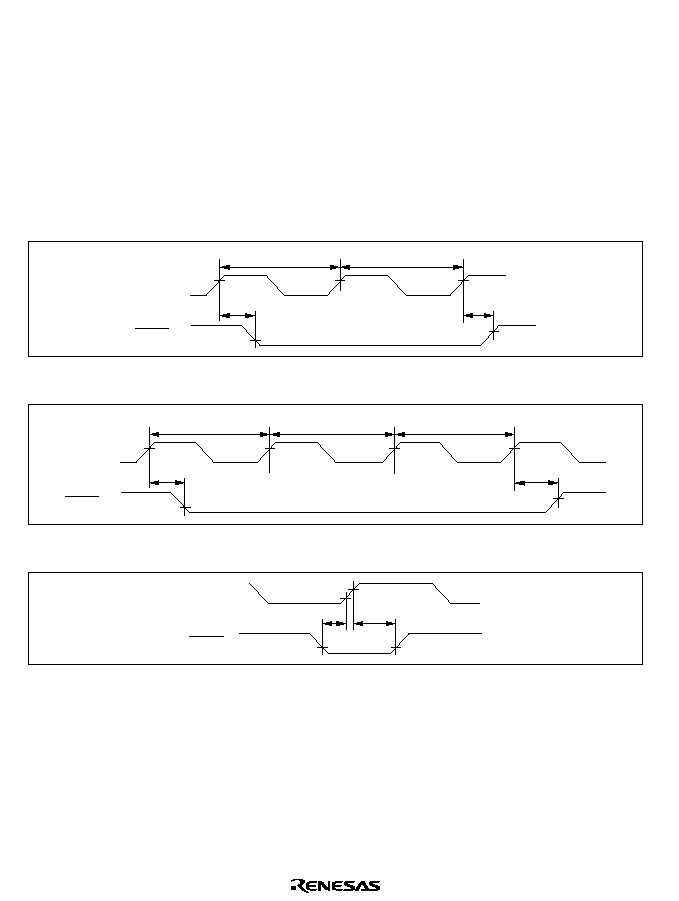
740
21.2.8
DMAC Timing
DMAC timing is shown as follows.
�
DMAC
TEND output timing for 2 state access
Figure 21.21 shows the DMAC
TEND output timing for two state access.
�
DMAC
TEND output timing for 3 state access
Figure 21.22 shows the DMAC
TEND output timing for three state access.
�
DMAC
DREQ input timing
Figure 21.23 shows DMAC
DREQ input timing.
T
1
T
2
t
TED1
t
TED2
TEND
Figure 21.21 DMAC
TEND Output Timing for two State Access
T
1
T
2
T
3
t
TED1
t
TED2
TEND
Figure 21.22 DMAC
TEND Output Timing for three State Access
t
DRQH
t
DRQS
DREQ
Figure 21.23 DMAC
DREQ Input Timing

741
Appendix A Instruction Set
A.1
Instruction List
Operand Notation
Symbol
Description
Rd
General destination register
Rs
General source register
Rn
General register
ERd
General destination register (address register or 32-bit register)
ERs
General source register (address register or 32-bit register)
ERn
General register (32-bit register)
(EAd)
Destination operand
(EAs)
Source operand
PC
Program counter
SP
Stack pointer
CCR
Condition code register
N
N (negative) flag in CCR
Z
Z (zero) flag in CCR
V
V (overflow) flag in CCR
C
C (carry) flag in CCR
disp
Displacement
Transfer from the operand on the left to the operand on the right, or transition from
the state on the left to the state on the right
+
Addition of the operands on both sides
�
Subtraction of the operand on the right from the operand on the left
�
Multiplication of the operands on both sides
�
Division of the operand on the left by the operand on the right
Logical AND of the operands on both sides
Logical OR of the operands on both sides
Exclusive logical OR of the operands on both sides
�
NOT (logical complement)
( ), < >
Contents of operand
Note: General registers include 8-bit registers (R0H to R7H and R0L to R7L) and 16-bit registers
(R0 to R7 and E0 to E7).

742
Condition Code Notation
Symbol
Description
�
Changed according to execution result
*
Undetermined (no guaranteed value)
0
Cleared to 0
1
Set to 1
--
Not affected by execution of the instruction
Varies depending on conditions, described in notes

743
Table A.1
Instruction Set
1. Data transfer instructions
Mnemonic
Operation
Condition Code
Operand Siz
e
#xx
Rn
@ERn
@(d,
ERn)
@�ERn/@ERn+
@aa
@(d,
PC)
@@aa
--
Addressing Mode and
Instruction Length (bytes)
Normal
Ad
v
anced
No. of
States
*
1
I
H
N
Z
V
C
MOV.B #xx:8, Rd
MOV.B Rs, Rd
MOV.B @ERs, Rd
MOV.B @(d:16, ERs),
Rd
MOV.B @(d:24, ERs),
Rd
MOV.B @ERs+, Rd
MOV.B @aa:8, Rd
MOV.B @aa:16, Rd
MOV.B @aa:24, Rd
MOV.B Rs, @ERd
MOV.B Rs, @(d:16,
ERd)
MOV.B Rs, @(d:24,
ERd)
MOV.B Rs, @�ERd
MOV.B Rs, @aa:8
MOV.B Rs, @aa:16
MOV.B Rs, @aa:24
MOV.W #xx:16, Rd
MOV.W Rs, Rd
MOV.W @ERs, Rd
MOV.W @(d:16, ERs),
Rd
MOV.W @(d:24, ERs),
Rd
MOV.W @ERs+, Rd
MOV.W @aa:16, Rd
B
B
B
B
B
B
B
B
B
B
B
B
B
B
B
B
W
W
W
W
W
W
W
2
2
2
4
8
2
2
4
6
2
4
8
2
2
4
6
4
2
2
4
8
2
4
#xx:8
Rd8
Rs8
Rd8
@ERs
Rd8
@(d:16, ERs)
Rd8
@(d:24, ERs)
Rd8
@ERs
Rd8
ERs32+1
ERs32
@aa:8
Rd8
@aa:16
Rd8
@aa:24
Rd8
Rs8
@ERd
Rs8
@(d:16, ERd)
Rs8
@(d:24, ERd)
ERd32�1
ERd32
Rs8
@ERd
Rs8
@aa:8
Rs8
@aa:16
Rs8
@aa:24
#xx:16
Rd16
Rs16
Rd16
@ERs
Rd16
@(d:16, ERs)
Rd16
@(d:24, ERs)
Rd16
@ERs
Rd16
ERs32+2
@ERd32
@aa:16
Rd16
2
2
4
6
10
6
4
6
8
4
6
10
6
4
6
8
4
2
4
6
10
6
6
-- --
�
�
0
--
-- --
�
�
0
--
-- --
�
�
0
--
-- --
�
�
0
--
-- --
�
�
0
--
-- --
�
�
0
--
-- --
�
�
0
--
-- --
�
�
0
--
-- --
�
�
0
--
-- --
�
�
0
--
-- --
�
�
0
--
-- --
�
�
0
--
-- --
�
�
0
--
-- --
�
�
0
--
-- --
�
�
0
--
-- --
�
�
0
--
-- --
�
�
0
--
-- --
�
�
0
--
-- --
�
�
0
--
-- --
�
�
0
--
-- --
�
�
0
--
-- --
�
�
0
--
-- --
�
�
0
--
744
Mnemonic
Operation
Condition Code
Operand Siz
e
#xx
Rn
@ERn
@(d,
ERn)
@�ERn/@ERn+
@aa
@(d,
PC)
@@aa
--
Addressing Mode and
Instruction Length (bytes)
Normal
Ad
v
anced
No. of
States
*
1
I
H
N
Z
V
C
MOV.W @aa:24, Rd
MOV.W Rs, @ERd
MOV.W Rs, @(d:16,
ERd)
MOV.W Rs, @(d:24,
ERd)
MOV.W Rs, @�ERd
MOV.W Rs, @aa:16
MOV.W Rs, @aa:24
MOV.L #xx:32, Rd
MOV.L ERs, ERd
MOV.L @ERs, ERd
MOV.L @(d:16, ERs),
ERd
MOV.L @(d:24, ERs),
ERd
MOV.L @ERs+, ERd
MOV.L @aa:16, ERd
MOV.L @aa:24, ERd
MOV.L ERs, @ERd
MOV.L ERs, @(d:16,
ERd)
MOV.L ERs, @(d:24,
ERd)
MOV.L ERs, @�ERd
MOV.L ERs, @aa:16
MOV.L ERs, @aa:24
POP.W Rn
POP.L ERn
W
W
W
W
W
W
W
L
L
L
L
L
L
L
L
L
L
L
L
L
L
W
L
6
2
4
8
2
4
6
6
2
4
6
10
4
6
8
4
6
10
4
6
8
2
4
@aa:24
Rd16
Rs16
@ERd
Rs16
@(d:16, ERd)
Rs16
@(d:24, ERd)
ERd32�2
ERd32
Rs16
@ERd
Rs16
@aa:16
Rs16
@aa:24
#xx:32
Rd32
ERs32
ERd32
@ERs
ERd32
@(d:16, ERs)
ERd32
@(d:24, ERs)
ERd32
@ERs
ERd32
ERs32+4
ERs32
@aa:16
ERd32
@aa:24
ERd32
ERs32
@ERd
ERs32
@(d:16, ERd)
ERs32
@(d:24, ERd)
ERd32�4
ERd32
ERs32
@ERd
ERs32
@aa:16
ERs32
@aa:24
@SP
Rn16
SP+2
SP
@SP
ERn32
SP+4
SP
8
4
6
10
6
6
8
6
2
8
10
14
10
10
12
8
10
14
10
10
12
6
10
-- --
�
�
0 --
-- --
�
�
0 --
-- --
�
�
0
--
-- --
�
�
0
--
-- --
�
�
0
--
-- --
�
�
0 --
-- --
�
�
0 --
-- --
�
�
0 --
-- --
�
�
0 --
-- --
�
�
0 --
-- --
�
�
0
--
-- --
�
�
0
--
-- --
�
�
0
--
-- --
�
�
0 --
-- --
�
�
0 --
-- --
�
�
0 --
-- --
�
�
0
--
-- --
�
�
0
--
-- --
�
�
0
--
-- --
�
�
0 --
-- --
�
�
0 --
-- --
�
�
0
--
-- --
�
�
0
--
745
Mnemonic
Operation
Condition Code
Operand Siz
e
#xx
Rn
@ERn
@(d,
ERn)
@�ERn/@ERn+
@aa
@(d,
PC)
@@aa
--
Addressing Mode and
Instruction Length (bytes)
Normal
Ad
v
anced
No. of
States
*
1
I
H
N
Z
V
C
PUSH.W Rn
PUSH.L ERn
MOVFPE @aa:16,
Rd
MOVTPE Rs,
@aa:16
W
L
B
B
2
4
4
4
SP�2
SP
Rn16
@SP
SP�4
SP
ERn32
@SP
Cannot be used in the
H8/3069F
Cannot be used in the
H8/3069F
6
10
-- --
�
�
0
--
-- --
�
�
0
--
Cannot be used in the
H8/3069F
Cannot be used in the
H8/3069F
2. Arithmetic instructions
Mnemonic
Operation
Condition Code
Operand Siz
e
#xx
Rn
@ERn
@(d,
ERn)
@�ERn/@ERn+
@aa
@(d,
PC)
@@aa
--
Addressing Mode and
Instruction Length (bytes)
Normal
Ad
v
anced
No. of
States
*
1
I
H
N
Z
V
C
ADD.B #xx:8, Rd
ADD.B Rs, Rd
ADD.W #xx:16, Rd
ADD.W Rs, Rd
ADD.L #xx:32, ERd
ADD.L ERs, ERd
ADDX.B #xx:8, Rd
ADDX.B Rs, Rd
ADDS.L #1, ERd
ADDS.L #2, ERd
ADDS.L #4, ERd
INC.B Rd
INC.W #1, Rd
INC.W #2, Rd
B
B
W
W
L
L
B
B
L
L
L
B
W
W
2
2
4
2
6
2
2
2
2
2
2
2
2
2
Rd8+#xx:8
Rd8
Rd8+Rs8
Rd8
Rd16+#xx:16
Rd16
Rd16+Rs16
Rd16
ERd32+#xx:32
ERd32
ERd32+ERs32
ERd32
Rd8+#xx:8 +C
Rd8
Rd8+Rs8 +C
Rd8
ERd32+1
ERd32
ERd32+2
ERd32
ERd32+4
ERd32
Rd8+1
Rd8
Rd16+1
Rd16
Rd16+2
Rd16
2
2
4
2
6
2
2
2
2
2
2
2
2
2
--
�
�
�
�
�
--
�
�
�
�
�
-- (1)
�
�
�
�
-- (1)
�
�
�
�
-- (2)
�
�
�
�
-- (2)
�
�
�
�
--
�
�
(3)
�
�
--
�
�
(3)
�
�
-- -- -- -- -- --
-- -- -- -- -- --
-- -- -- -- -- --
-- --
�
�
�
--
-- --
�
�
�
--
-- --
�
�
�
--
746
Mnemonic
Operation
Condition Code
Operand Siz
e
#xx
Rn
@ERn
@(d,
ERn)
@�ERn/@ERn+
@aa
@(d,
PC)
@@aa
--
Addressing Mode and
Instruction Length (bytes)
Normal
Ad
v
anced
No. of
States
*
1
I
H
N
Z
V
C
INC.L #1, ERd
INC.L #2, ERd
DAA Rd
SUB.B Rs, Rd
SUB.W #xx:16, Rd
SUB.W Rs, Rd
SUB.L #xx:32, ERd
SUB.L ERs, ERd
SUBX.B #xx:8, Rd
SUBX.B Rs, Rd
SUBS.L #1, ERd
SUBS.L #2, ERd
SUBS.L #4, ERd
DEC.B Rd
DEC.W #1, Rd
DEC.W #2, Rd
DEC.L #1, ERd
DEC.L #2, ERd
DAS.Rd
MULXU. B Rs, Rd
MULXU. W Rs, ERd
MULXS. B Rs, Rd
MULXS. W Rs, ERd
DIVXU. B Rs, Rd
L
L
B
B
W
W
L
L
B
B
L
L
L
B
W
W
L
L
B
B
W
B
W
B
2
2
2
2
4
2
6
2
2
2
2
2
2
2
2
2
2
2
2
2
2
4
4
2
ERd32+1
ERd32
ERd32+2
ERd32
Rd8 decimal adjust
Rd8
Rd8�Rs8
Rd8
Rd16�#xx:16
Rd16
Rd16�Rs16
Rd16
ERd32�#xx:32
ERd32
ERd32�ERs32
ERd32
Rd8�#xx:8�C
Rd8
Rd8�Rs8�C
Rd8
ERd32�1
ERd32
ERd32�2
ERd32
ERd32�4
ERd32
Rd8�1
Rd8
Rd16�1
Rd16
Rd16�2
Rd16
ERd32�1
ERd32
ERd32�2
ERd32
Rd8 decimal adjust
Rd8
Rd8
�
Rs8
Rd16
(unsigned multiplication)
Rd16
�
Rs16
ERd32
(unsigned multiplication)
Rd8
�
Rs8
Rd16
(signed multiplication)
Rd16
�
Rs16
ERd32
(signed multiplication)
Rd16
�
Rs8
Rd16
(RdH: remainder, RdL:
quotient)
(unsigned division)
2
2
2
2
4
2
6
2
2
2
2
2
2
2
2
2
2
2
2
14
22
16
24
14
-- --
�
�
�
--
-- --
�
�
�
--
--
*
�
�
*
--
--
�
�
�
�
�
-- (1)
�
�
�
�
-- (1)
�
�
�
�
-- (2)
�
�
�
�
-- (2)
�
�
�
�
--
�
�
(3)
�
�
--
�
�
(3)
�
�
-- -- -- -- -- --
-- -- -- -- -- --
-- -- -- -- -- --
-- --
�
�
�
--
-- --
�
�
�
--
-- --
�
�
�
--
-- --
�
�
�
--
-- --
�
�
�
--
--
*
�
�
*
--
-- -- -- -- -- --
--
-- -- -- -- --
-- --
�
�
-- --
-- --
�
�
-- --
-- -- (6) (7) -- --
747
Mnemonic
Operation
Condition Code
Operand Siz
e
#xx
Rn
@ERn
@(d,
ERn)
@�ERn/@ERn+
@aa
@(d,
PC)
@@aa
--
Addressing Mode and
Instruction Length (bytes)
Normal
Ad
v
anced
No. of
States
*
1
I
H
N
Z
V
C
DIVXU. W Rs, ERd
DIVXS. B Rs, Rd
DIVXS. W Rs, ERd
CMP.B #xx:8, Rd
CMP.B Rs, Rd
CMP.W #xx:16, Rd
CMP.W Rs, Rd
CMP.L #xx:32, ERd
CMP.L ERs, ERd
NEG.B Rd
NEG.W Rd
NEG.L ERd
EXTU.W Rd
EXTU.L ERd
EXTS.W Rd
EXTS.L ERd
W
B
W
B
B
W
W
L
L
B
W
L
W
L
W
L
2
4
4
2
2
4
2
6
2
2
2
2
2
2
2
2
ERd32
�
Rs16
ERd32
(Ed: remainder,
Rd: quotient)
(unsigned division)
Rd16
�
Rs8
Rd16
(RdH: remainder,
RdL: quotient)
(signed division)
ERd32
�
Rs16
ERd32
(Ed: remainder,
Rd: quotient)
(signed division)
Rd8�#xx:8
Rd8�Rs8
Rd16�#xx:16
Rd16�Rs16
ERd32�#xx:32
ERd32�ERs32
0�Rd8
Rd8
0�Rd16
Rd16
0�ERd32
ERd32
0
(<bits 15 to 8>
of Rd16)
0
(<bits 31 to 16>
of ERd32)
(<bit 7> of Rd16)
(<bits 15 to 8> of Rd16)
(<bit 15> of ERd32)
(<bits 31 to 16> of
ERd32)
22
16
24
2
2
4
2
6
2
2
2
2
2
2
2
2
-- -- (6) (7) -- --
-- -- (8) (7) -- --
-- -- (8) (7) -- --
--
�
�
�
�
�
--
�
�
�
�
�
-- (1)
�
�
�
�
-- (1)
�
�
�
�
-- (2)
�
�
�
�
-- (2)
�
�
�
�
--
�
�
�
�
�
--
�
�
�
�
�
--
�
�
�
�
�
-- --
0
�
0
--
-- --
0
�
0
--
-- --
�
�
0
�
-- --
�
�
0
--
748
3. Logic instructions
Mnemonic
Operation
Condition Code
Operand Siz
e
#xx
Rn
@ERn
@(d,
ERn)
@�ERn/@ERn+
@aa
@(d,
PC)
@@aa
--
Addressing Mode and
Instruction Length (bytes)
Normal
Ad
v
anced
No. of
States
*
1
I
H
N
Z
V
C
AND.B #xx:8, Rd
AND.B Rs, Rd
AND.W #xx:16, Rd
AND.W Rs, Rd
AND.L #xx:32, ERd
AND.L ERs, ERd
OR.B #xx:8, Rd
OR.B Rs, Rd
OR.W #xx:16, Rd
OR.W Rs, Rd
OR.L #xx:32, ERd
OR.L ERs, ERd
XOR.B #xx:8, Rd
XOR.B Rs, Rd
XOR.W #xx:16, Rd
XOR.W Rs, Rd
XOR.L #xx:32, ERd
XOR.L ERs, ERd
NOT.B Rd
NOT.W Rd
NOT.L ERd
B
B
W
W
L
L
B
B
W
W
L
L
B
B
W
W
L
L
B
W
L
2
2
4
2
6
4
2
2
4
2
6
4
2
2
4
2
6
4
2
2
2
Rd8
#xx:8
Rd8
Rd8
Rs8
Rd8
Rd16
#xx:16
Rd16
Rd16
Rs16
Rd16
ERd32
#xx:32
ERd32
ERd32
ERs32
ERd32
Rd8
/
#xx:8
Rd8
Rd8
/
Rs8
Rd8
Rd16
/
#xx:16
Rd16
Rd16
/
Rs16
Rd16
ERd32
/
#xx:32
ERd32
ERd32
/
ERs32
ERd32
Rd8
#xx:8
Rd8
Rd8
Rs8
Rd8
Rd16
#xx:16
Rd16
Rd16
Rs16
Rd16
ERd32
#xx:32
ERd32
ERd32
ERs32
ERd32
�Rd8
Rd8
�Rd16
Rd16
�Rd32
Rd32
2
2
4
2
6
4
2
2
4
2
6
4
2
2
4
2
6
4
2
2
2
-- --
�
�
0
--
-- --
�
�
0
--
-- --
�
�
0
--
-- --
�
�
0
--
-- --
�
�
0
--
-- --
�
�
0
--
-- --
�
�
0
--
-- --
�
�
0
--
-- --
�
�
0
--
-- --
�
�
0
--
-- --
�
�
0
--
-- --
�
�
0
--
-- --
�
�
0
--
-- --
�
�
0
--
-- --
�
�
0
--
-- --
�
�
0
--
-- --
�
�
0
--
-- --
�
�
0
--
-- --
�
�
0
--
-- --
�
�
0
--
-- --
�
�
0
--
749
4. Shift instructions
Mnemonic
Operation
Condition Code
Operand Siz
e
#xx
Rn
@ERn
@(d,
ERn)
@�ERn/@ERn+
@aa
@(d,
PC)
@@aa
--
Addressing Mode and
Instruction Length (bytes)
Normal
Ad
v
anced
No. of
States
*
1
I
H
N
Z
V
C
SHAL.B Rd
SHAL.W Rd
SHAL.L ERd
SHAR.B Rd
SHAR.W Rd
SHAR.L ERd
SHLL.B Rd
SHLL.W Rd
SHLL.L ERd
SHLR.B Rd
SHLR.W Rd
SHLR.L ERd
ROTXL.B Rd
ROTXL.W Rd
ROTXL.L ERd
ROTXR.B Rd
ROTXR.W Rd
ROTXR.L ERd
ROTL.B Rd
ROTL.W Rd
ROTL.L ERd
ROTR.B Rd
ROTR.W Rd
ROTR.L ERd
B
W
L
B
W
L
B
W
L
B
W
L
B
W
L
B
W
L
B
W
L
B
W
L
2
2
2
2
2
2
2
2
2
2
2
2
2
2
2
2
2
2
2
2
2
2
2
2
2
2
2
2
2
2
2
2
2
2
2
2
2
2
2
2
2
2
2
2
2
2
2
2
-- --
�
�
�
�
-- --
�
�
�
�
-- --
�
�
�
�
-- --
�
�
0
�
-- --
�
�
0
�
-- --
�
�
0
�
-- --
�
�
0
�
-- --
�
�
0
�
-- --
�
�
0
�
-- --
�
�
0
�
-- --
�
�
0
�
-- --
�
�
0
�
-- --
�
�
0
�
-- --
�
�
0
�
-- --
�
�
0
�
-- --
�
�
0
�
-- --
�
�
0
�
-- --
�
�
0
�
-- --
�
�
0
�
-- --
�
�
0
�
-- --
�
�
0
�
-- --
�
�
0
�
-- --
�
�
0
�
-- --
�
�
0
�
C
MSB
LSB
C
MSB
LSB
C
MSB
LSB
C
MSB
LSB
MSB
LSB
0
C
MSB
LSB
0
C
C
MSB
LSB
0
C
MSB
LSB
750
5. Bit manipulation instructions
Mnemonic
Operation
Condition Code
Operand Siz
e
#xx
Rn
@ERn
@(d,
ERn)
@�ERn/@ERn+
@aa
@(d,
PC)
@@aa
--
Addressing Mode and
Instruction Length (bytes)
Normal
Ad
v
anced
No. of
States
*
1
I
H
N
Z
V
C
BSET #xx:3, Rd
BSET #xx:3, @ERd
BSET #xx:3, @aa:8
BSET Rn, Rd
BSET Rn, @ERd
BSET Rn, @aa:8
BCLR #xx:3, Rd
BCLR #xx:3, @ERd
BCLR #xx:3, @aa:8
BCLR Rn, Rd
BCLR Rn, @ERd
BCLR Rn, @aa:8
BNOT #xx:3, Rd
BNOT #xx:3, @ERd
BNOT #xx:3, @aa:8
BNOT Rn, Rd
BNOT Rn, @ERd
BNOT Rn, @aa:8
BTST #xx:3, Rd
BTST #xx:3, @ERd
BTST #xx:3, @aa:8
BTST Rn, Rd
BTST Rn, @ERd
BTST Rn, @aa:8
BLD #xx:3, Rd
B
B
B
B
B
B
B
B
B
B
B
B
B
B
B
B
B
B
B
B
B
B
B
B
B
2
4
4
2
4
4
2
4
4
2
4
4
2
4
4
2
4
4
2
4
4
2
4
4
2
(#xx:3 of Rd8)
1
(#xx:3 of @ERd)
1
(#xx:3 of @aa:8)
1
(Rn8 of Rd8)
1
(Rn8 of @ERd)
1
(Rn8 of @aa:8)
1
(#xx:3 of Rd8)
0
(#xx:3 of @ERd)
0
(#xx:3 of @aa:8)
0
(Rn8 of Rd8)
0
(Rn8 of @ERd)
0
(Rn8 of @aa:8)
0
(#xx:3 of Rd8)
� (#xx:3 of Rd8)
(#xx:3 of @ERd)
� (#xx:3 of @ERd)
(#xx:3 of @aa:8)
� (#xx:3 of @aa:8)
(Rn8 of Rd8)
� (Rn8 of Rd8)
(Rn8 of @ERd)
� (Rn8 of @ERd)
(Rn8 of @aa:8)
� (Rn8 of @aa:8)
� (#xx:3 of Rd8)
Z
� (#xx:3 of @ERd)
Z
� (#xx:3 of @aa:8)
Z
� (Rn8 of @Rd8)
Z
� (Rn8 of @ERd)
Z
� (Rn8 of @aa:8)
Z
(#xx:3 of Rd8)
C
2
8
8
2
8
8
2
8
8
2
8
8
2
8
8
2
8
8
2
6
6
2
6
6
2
-- -- -- -- -- --
-- -- -- -- -- --
-- -- -- -- -- --
-- -- -- -- -- --
-- -- -- -- -- --
-- -- -- -- -- --
-- -- -- -- -- --
-- -- -- -- -- --
-- -- -- -- -- --
-- -- -- -- -- --
-- -- -- -- -- --
-- -- -- -- -- --
-- -- -- -- -- --
-- -- -- -- -- --
-- -- -- -- -- --
-- -- -- -- -- --
-- -- -- -- -- --
-- -- -- -- -- --
-- -- --
�
-- --
-- -- --
�
-- --
-- -- --
�
-- --
-- -- --
�
-- --
-- -- --
�
-- --
-- -- --
�
-- --
-- -- -- -- --
�
751
Mnemonic
Operation
Condition Code
Operand Siz
e
#xx
Rn
@ERn
@(d,
ERn)
@�ERn/@ERn+
@aa
@(d,
PC)
@@aa
--
Addressing Mode and
Instruction Length (bytes)
Normal
Ad
v
anced
No. of
States
*
1
I
H
N
Z
V
C
BLD #xx:3, @ERd
BLD #xx:3, @aa:8
BILD #xx:3, Rd
BILD #xx:3, @ERd
BILD #xx:3, @aa:8
BST #xx:3, Rd
BST #xx:3, @ERd
BST #xx:3, @aa:8
BIST #xx:3, Rd
BIST #xx:3, @ERd
BIST #xx:3, @aa:8
BAND #xx:3, Rd
BAND #xx:3, @ERd
BAND #xx:3, @aa:8
BIAND #xx:3, Rd
BIAND #xx:3, @ERd
BIAND #xx:3, @aa:8
BOR #xx:3, Rd
BOR #xx:3, @ERd
BOR #xx:3, @aa:8
BIOR #xx:3, Rd
BIOR #xx:3, @ERd
BIOR #xx:3, @aa:8
BXOR #xx:3, Rd
BXOR #xx:3, @ERd
BXOR #xx:3, @aa:8
BIXOR #xx:3, Rd
BIXOR #xx:3, @ERd
BIXOR #xx:3, @aa:8
B
B
B
B
B
B
B
B
B
B
B
B
B
B
B
B
B
B
B
B
B
B
B
B
B
B
B
B
B
4
4
2
4
4
2
4
4
2
4
4
2
4
4
2
4
4
2
4
4
2
4
4
2
4
4
2
4
4
(#xx:3 of @ERd)
C
(#xx:3 of @aa:8)
C
� (#xx:3 of Rd8)
C
� (#xx:3 of @ERd)
C
� (#xx:3 of @aa:8)
C
C
(#xx:3 of Rd8)
C
(#xx:3 of @ERd24)
C
(#xx:3 of @aa:8)
� C
(#xx:3 of Rd8)
� C
(#xx:3 of @ERd24)
� C
(#xx:3 of @aa:8)
C
(#xx:3 of Rd8)
C
C
(#xx:3 of @ERd24)
C
C
(#xx:3 of @aa:8)
C
C
� (#xx:3 of Rd8)
C
C
� (#xx:3 of @ERd24)
C
C
� (#xx:3 of @aa:8)
C
C
/
(#xx:3 of Rd8)
C
C
/
(#xx:3 of @ERd24)
C
C
/
(#xx:3 of @aa:8)
C
C
/
� (#xx:3 of Rd8)
C
C
/
� (#xx:3 of @ERd24)
C
C
/
� (#xx:3 of @aa:8)
C
C
(#xx:3 of Rd8)
C
C
(#xx:3 of @ERd24)
C
C
(#xx:3 of @aa:8)
C
C
� (#xx:3 of Rd8)
C
C
� (#xx:3 of @ERd24)
C
C
� (#xx:3 of @aa:8)
C
6
6
2
6
6
2
8
8
2
8
8
2
6
6
2
6
6
2
6
6
2
6
6
2
6
6
2
6
6
-- -- -- -- --
�
-- -- -- -- --
�
-- -- -- -- --
�
-- -- -- -- --
�
-- -- -- -- --
�
-- -- -- -- -- --
-- -- -- -- -- --
-- -- -- -- -- --
-- -- -- -- -- --
-- -- -- -- -- --
-- -- -- -- -- --
-- -- -- -- --
�
-- -- -- -- --
�
-- -- -- -- --
�
-- -- -- -- --
�
-- -- -- -- --
�
-- -- -- -- --
�
-- -- -- -- --
�
-- -- -- -- --
�
-- -- -- -- --
�
-- -- -- -- --
�
-- -- -- -- --
�
-- -- -- -- --
�
-- -- -- -- --
�
-- -- -- -- --
�
-- -- -- -- --
�
-- -- -- -- --
�
-- -- -- -- --
�
-- -- -- -- --
�
752
6. Branching instructions
Mnemonic
Operation
Branch
Condition
Condition Code
Operand Siz
e
#xx
Rn
@ERn
@(d,
ERn)
@�ERn/@ERn+
@aa
@(d,
PC)
@@aa
--
Addressing Mode and
Instruction Length (bytes)
Normal
Ad
v
anced
No. of
States
*
1
I
H
N
Z
V
C
BRA d:8 (BT d:8)
BRA d:16 (BT d:16)
BRN d:8 (BF d:8)
BRN d:16 (BF d:16)
BHI d:8
BHI d:16
BLS d:8
BLS d:16
BCC d:8 (BHS d:8)
BCC d:16 (BHS d:16)
BCS d:8 (BLO d:8)
BCS d:16 (BLO d:16)
BNE d:8
BNE d:16
BEQ d:8
BEQ d:16
BVC d:8
BVC d:16
BVS d:8
BVS d:16
BPL d:8
BPL d:16
BMI d:8
BMI d:16
BGE d:8
BGE d:16
BLT d:8
BLT d:16
BGT d:8
BGT d:16
--
--
--
--
--
--
--
--
--
--
--
--
--
--
--
--
--
--
--
--
--
--
--
--
--
--
--
--
--
--
2
4
2
4
2
4
2
4
2
4
2
4
2
4
2
4
2
4
2
4
2
4
2
4
2
4
2
4
2
4
If condition
is true then
PC
PC+d else
next;
4
6
4
6
4
6
4
6
4
6
4
6
4
6
4
6
4
6
4
6
4
6
4
6
4
6
4
6
4
6
-- -- -- -- -- --
-- -- -- -- -- --
-- -- -- -- -- --
-- -- -- -- -- --
-- -- -- -- -- --
-- -- -- -- -- --
-- -- -- -- -- --
-- -- -- -- -- --
-- -- -- -- -- --
-- -- -- -- -- --
-- -- -- -- -- --
-- -- -- -- -- --
-- -- -- -- -- --
-- -- -- -- -- --
-- -- -- -- -- --
-- -- -- -- -- --
-- -- -- -- -- --
-- -- -- -- -- --
-- -- -- -- -- --
-- -- -- -- -- --
-- -- -- -- -- --
-- -- -- -- -- --
-- -- -- -- -- --
-- -- -- -- -- --
-- -- -- -- -- --
-- -- -- -- -- --
-- -- -- -- -- --
-- -- -- -- -- --
-- -- -- -- -- --
-- -- -- -- -- --
Always
Never
C
/
Z = 0
C
/
Z = 1
C = 0
C = 1
Z = 0
Z = 1
V = 0
V = 1
N = 0
N = 1
N
V = 0
N
V = 1
Z
/
(N
V)
= 0
753
Mnemonic
Operation
Operation
Condition Code
Operand Siz
e
#xx
Rn
@ERn
@(d,
ERn)
@�ERn/@ERn+
@aa
@(d,
PC)
@@aa
--
Addressing Mode and
Instruction Length (bytes)
Normal
Ad
v
anced
No. of
States
*
1
I
H
N
Z
V
C
BLE d:8
BLE d:16
JMP @ERn
JMP @aa:24
JMP @@aa:8
BSR d:8
BSR d:16
JSR @ERn
JSR @aa:24
JSR @@aa:8
RTS
--
--
--
--
--
--
--
--
--
--
--
2
4
2
4
2
2
4
2
4
2
2
PC
ERn
PC
aa:24
PC
@aa:8
PC
@�SP
PC
PC+d:8
PC
@�SP
PC
PC+d:16
PC
@�SP
PC
@ERn
PC
@�SP
PC
@aa:24
PC
@�SP
PC
@aa:8
PC
@SP+
4
6
4
6
8
6
8
6
8
8
8
10
8
10
8
10
12
10
-- -- -- -- -- --
-- -- -- -- -- --
-- -- -- -- -- --
-- -- -- -- -- --
-- -- -- -- -- --
-- -- -- -- -- --
-- -- -- -- -- --
-- -- -- -- -- --
-- -- -- -- -- --
-- -- -- -- -- --
-- -- -- -- -- --
Branch
Condition
If condition
is true then
PC
PC+d
else next;
Z
/
(N
V) = 1
754
7. System control instructions
Mnemonic
Operation
Condition Code
Operand Siz
e
#xx
Rn
@ERn
@(d,
ERn)
@�ERn/@ERn+
@aa
@(d,
PC)
@@aa
--
Addressing Mode and
Instruction Length (bytes)
Normal
Ad
v
anced
No. of
States
*
1
I
H
N
Z
V
C
TRAPA #x:2
RTE
SLEEP
LDC #xx:8, CCR
LDC Rs, CCR
LDC @ERs, CCR
LDC @(d:16, ERs),
CCR
LDC @(d:24, ERs),
CCR
LDC @ERs+, CCR
LDC @aa:16, CCR
LDC @aa:24, CCR
STC CCR, Rd
STC CCR, @ERd
STC CCR, @(d:16,
ERd)
STC CCR, @(d:24,
ERd)
STC CCR, @�ERd
STC CCR, @aa:16
STC CCR, @aa:24
ANDC #xx:8, CCR
ORC #xx:8, CCR
XORC #xx:8, CCR
NOP
--
--
--
B
B
W
W
W
W
W
W
B
W
W
W
W
W
W
B
B
B
--
2
2
2
4
6
10
4
6
8
2
4
6
10
4
6
8
2
2
2
2
PC
@�SP
CCR
@�SP
<vector>
PC
CCR
@SP+
PC
@SP+
Transition to powerdown
state
#xx:8
CCR
Rs8
CCR
@ERs
CCR
@(d:16, ERs)
CCR
@(d:24, ERs)
CCR
@ERs
CCR
ERs32+2
ERs32
@aa:16
CCR
@aa:24
CCR
CCR
Rd8
CCR
@ERd
CCR
@(d:16, ERd)
CCR
@(d:24, ERd)
ERd32�2
ERd32
CCR
@ERd
CCR
@aa:16
CCR
@aa:24
CCR
#xx:8
CCR
CCR
/
#xx:8
CCR
CCR
#xx:8
CCR
PC
PC+2
10
2
2
2
6
8
12
8
8
10
2
6
8
12
8
8
10
2
2
2
2
1
-- -- -- -- --
�
�
�
�
�
�
-- -- -- -- -- --
�
�
�
�
�
�
�
�
�
�
�
�
�
�
�
�
�
�
�
�
�
�
�
�
�
�
�
�
�
�
�
�
�
�
�
�
�
�
�
�
�
�
�
�
�
�
�
�
-- -- -- -- -- --
-- -- -- -- -- --
-- -- -- -- -- --
-- -- -- -- -- --
-- -- -- -- -- --
-- -- -- -- -- --
-- -- -- -- -- --
�
�
�
�
�
�
�
�
�
�
�
�
�
�
�
�
�
�
-- -- -- -- -- --
14 16
755
8. Block transfer instructions
Mnemonic
Operation
Condition Code
Operand Siz
e
#xx
Rn
@ERn
@(d,
ERn)
@�ERn/@ERn+
@aa
@(d,
PC)
@@aa
--
Addressing Mode and
Instruction Length (bytes)
Normal
Ad
v
anced
No. of
States
*
1
I
H
N
Z
V
C
EEPMOV. B
EEPMOV. W
--
--
4
4
if R4L
0
repeat @R5
@R6
R5+1
R5
R6+1
R6
R4L�1
R4L
until
R4L=0
else next;
if R4
0
repeat @R5
@R6
R5+1
R5
R6+1
R6
R4�1
R4
until
R4=0
else next;
8+
4n
*
2
8+
4n
*
2
-- -- -- -- -- --
-- -- -- -- -- --
Notes:
*
1 The number of states is the number of states required for execution when the
instruction and its operands are located in on-chip memory. For other cases see section
A.3.
*
2 n is the value set in register R4L or R4.
(1) Set to 1 when a carry or borrow occurs at bit 11; otherwise cleared to 0.
(2) Set to 1 when a carry or borrow occurs at bit 27; otherwise cleared to 0.
(3) Retains its previous value when the result is zero; otherwise cleared to 0.
(4) Set to 1 when the adjustment produces a carry; otherwise retains its previous value.
(5) The number of states required for execution of an instruction that transfers data in
synchronization with the E clock is variable.
(6) Set to 1 when the divisor is negative; otherwise cleared to 0.
(7) Set to 1 when the divisor is zero; otherwise cleared to 0.
(8) Set to 1 when the quotient is negative; otherwise cleared to 0.
756
A.2
Operation Code Maps
Table A.2
Operation Code Map (1)
AH
AL
0123
4567
89
A
B
C
D
E
F
0
1
2
3
4
5
6
7
8
9
A
B
C
D
E
F
NOP
BRA
MULXU
BSET
BRN
DIVXU
BNOT
STC
BHI
MULXU
BCLR
LDC
BLS
DIVXU
BTST
ORC
OR.B
BCC
RTS
OR
XORC
XOR.B
BCS
BSR
XOR
BOR
BIOR
BXOR
BIXOR
BAND
BIAND
ANDC
AND.B
BNE
RTE
AND
LDC
BNQ
TRAPA
BLD
BILD
BST
BIST
BVC
MOV
BPL
JMP
BMI
ADDX
SUBX
BGT
JSR
BLE
MOV
ADD
ADDX
CMP
SUBX
OR
XOR
AND
MOV
A.2 Operation Code Map (1)
Instruction when most significant bit of BH is 0.
Instruction when most significant bit of BH is 1.
Instruction code:
Table A.2
(2)
Table A.2
(2)
Table A.2
(2)
Table A.2
(2)
Table A.2
(2)
BVS
BLT
BGE
BSR
Table A.2
(2)
Table A.2
(2)
Table A.2
(2)
Table A.2
(2)
Table A.2
(2)
Table A.2
(2)
Table A.2
(2)
Table A.2
(2)
Table A.2
(2)
Table A.2
(2)
Table A.2
(3)
1st byte
2nd byte
AH
BH
AL
BL
ADD
SUB
MOV
CMP
MOV.B
EEPMOV
757
Table A.2
Operation Code Map (2)
AH AL
BH
0123
4567
89
A
B
C
D
E
F
01
0A
0B
0F
10
11
12
13
17
1A
1B
1F
58
79
7A
MOV
INC
ADDS
DAA
DEC
SUBS
DAS
BRA
MOV
MOV
BHI
CMP
CMP
LDC/STC
BCC
OR
OR
BPL
BGT
Instruction code:
BVS
SLEEP
BVC
BGE
Table A.2
(3)
Table A.2
(3)
Table A.2
(3)
BNE
AND
AND
INC
EXTU
DEC
BEQ
INC
EXTU
DEC
BCS
XOR
XOR
SHLL
SHLR
ROTXL
ROTXR
NOT
BLS
SUB
SUB
BRN
ADD
ADD
INC
EXTS
DEC
BLT
INC
EXTS
DEC
BLE
SHAL
SHAR
ROTL
ROTR
NEG
BMI
1st byte
2nd byte
AH
BH
AL
BL
SUBS
ADDS
ADD
MOV
SUB
CMP
SHLL
SHLR
ROTXL
ROTXR
NOT
SHAL
SHAR
ROTL
ROTR
NEG
758
Table A.2
Operation Code Map (3)
AH
ALBH
BLCH
CL
0123
4567
89
A
B
C
D
E
F
01406
01C05
01D05
01F06
7Cr06
7Cr07
7Dr06
7Dr07
7Eaa6
7Eaa7
7Faa6
7Faa7
MULXS
BSET
BSET
BSET
BSET
DIVIXS
BNOT
BNOT
BNOT
BNOT
MULXS
BCLR
BCLR
BCLR
BCLR
DIVXS
BTST
BTST
BTST
BTST
OR
XOR
BOR
BIOR
BXOR
BIXOR
BAND
BIAND
AND
BLD
BILD
BST
BIST
Instruction when most significant bit of DH is 0.
Instruction when most significant bit of DH is 1.
Instruction code:
*
*
*
*
*
*
*
*
1
1
1
1
2
2
2
2
BOR
BIOR
BXOR
BIXOR
BAND
BIAND
BLD
BILD
BST
BIST
Notes:
*
1
*
2
r is the register designation field.
aa is the absolute address field.
1st byte
2nd byte
AH
BH
AL
BL
3rd byte
CH
DH
CL
DL
4th byte
LDC
STC
LDC
LDC
LDC
STC
STC
STC

759
A.3
Number of States Required for Execution
The tables in this section can be used to calculate the number of states required for instruction
execution by the H8/300H CPU. Table A.4 indicates the number of instruction fetch, data
read/write, and other cycles occurring in each instruction. Table A.3 indicates the number of states
required per cycle according to the bus size. The number of states required for execution of an
instruction can be calculated from these two tables as follows:
Number of states = I
�
S
I
+ J
�
S
J
+ K
�
S
K
+ L
�
S
L
+ M
�
S
M
+ N
�
S
N
Examples of Calculation of Number of States Required for Execution
Examples: Advanced mode, stack located in external address space, on-chip supporting modules
accessed with 8-bit bus width, external devices accessed in three states with one wait state and
16-bit bus width.
BSET #0, @FFFFC7:8
From table A.4, I = L = 2 and J = K = M = N = 0
From table A.3, S
I
= 4 and S
L
= 3
Number of states = 2
�
4 + 2
�
3 = 14
JSR @@30
From table A.4, I = J = K = 2 and L = M = N = 0
From table A.3, S
I
= S
J
= S
K
= 4
Number of states = 2
�
4 + 2
�
4 + 2
�
4 = 24

760
Table A.3
Number of States per Cycle
Access Conditions
On-Chip Sup-
External Device
porting Module
8-Bit Bus
16-Bit Bus
Execution State
(Cycle)
On-Chip
Memory
8-Bit
Bus
16-Bit
Bus
2-State
Access
3-State
Access
2-State
Access
3-State
Access
Instruction fetch
S
I
2
6
3
4
6 + 2m
2
3 + m
Branch address read S
J
Stack operation
S
K
Byte data access
S
L
3
2
3 + m
Word data access
S
M
6
4
6 + 2m
Internal operation
S
N
1
Legend
m: Number of wait states inserted into external device access

761
Table A.4
Number of Cycles per Instruction
Instruction Mnemonic
Instruction
Fetch
I
Branch
Addr. Read
J
Stack
Operation
K
Byte Data
Access
L
Word Data
Access
M
Internal
Operation
N
ADD
ADD.B #xx:8, Rd
ADD.B Rs, Rd
ADD.W #xx:16, Rd
ADD.W Rs, Rd
ADD.L #xx:32, ERd
ADD.L ERs, ERd
1
1
2
1
3
1
ADDS
ADDS #1/2/4, ERd
1
ADDX
ADDX #xx:8, Rd
ADDX Rs, Rd
1
1
AND
AND.B #xx:8, Rd
AND.B Rs, Rd
AND.W #xx:16, Rd
AND.W Rs, Rd
AND.L #xx:32, ERd
AND.L ERs, ERd
1
1
2
1
3
2
ANDC
ANDC #xx:8, CCR
1
BAND
BAND #xx:3, Rd
BAND #xx:3, @ERd
BAND #xx:3, @aa:8
1
2
2
1
1
Bcc
BRA d:8 (BT d:8)
BRN d:8 (BF d:8)
BHI d:8
BLS d:8
BCC d:8 (BHS d:8)
BCS d:8 (BLO d:8)
BNE d:8
BEQ d:8
BVC d:8
BVS d:8
BPL d:8
BMI d:8
BGE d:8
BLT d:8
BGT d:8
BLE d:8
2
2
2
2
2
2
2
2
2
2
2
2
2
2
2
2

762
Instruction Mnemonic
Instruction
Fetch
I
Branch
Addr. Read
J
Stack
Operation
K
Byte Data
Access
L
Word Data
Access
M
Internal
Operation
N
Bcc
BRA d:16 (BT d:16)
BRN d:16 (BF d:16)
BHI d:16
BLS d:16
BCC d:16 (BHS d:16)
BCS d:16 (BLO d:16)
BNE d:16
BEQ d:16
BVC d:16
BVS d:16
BPL d:16
BMI d:16
BGE d:16
BLT d:16
BGT d:16
BLE d:16
2
2
2
2
2
2
2
2
2
2
2
2
2
2
2
2
2
2
2
2
2
2
2
2
2
2
2
2
2
2
2
2
BCLR
BCLR #xx:3, Rd
BCLR #xx:3, @ERd
BCLR #xx:3, @aa:8
BCLR Rn, Rd
BCLR Rn, @ERd
BCLR Rn, @aa:8
1
2
2
1
2
2
2
2
2
2
BIAND
BIAND #xx:3, Rd
BIAND #xx:3, @ERd
BIAND #xx:3, @aa:8
1
2
2
1
1
BILD
BILD #xx:3, Rd
BILD #xx:3, @ERd
BILD #xx:3, @aa:8
1
2
2
1
1
BIOR
BIOR #xx:8, Rd
BIOR #xx:8, @ERd
BIOR #xx:8, @aa:8
1
2
2
1
1
BIST
BIST #xx:3, Rd
BIST #xx:3, @ERd
BIST #xx:3, @aa:8
1
2
2
2
2
BIXOR
BIXOR #xx:3, Rd
BIXOR #xx:3, @ERd
BIXOR #xx:3, @aa:8
1
2
2
1
1
BLD
BLD #xx:3, Rd
BLD #xx:3, @ERd
BLD #xx:3, @aa:8
1
2
2
1
1

763
Instruction Mnemonic
Instruction
Fetch
I
Branch
Addr. Read
J
Stack
Operation
K
Byte Data
Access
L
Word Data
Access
M
Internal
Operation
N
BNOT
BNOT #xx:3, Rd
BNOT #xx:3, @ERd
BNOT #xx:3, @aa:8
BNOT Rn, Rd
BNOT Rn, @ERd
BNOT Rn, @aa:8
1
2
2
1
2
2
2
2
2
2
BOR
BOR #xx:3, Rd
BOR #xx:3, @ERd
BOR #xx:3, @aa:8
1
2
2
1
1
BSET
BSET #xx:3, Rd
BSET #xx:3, @ERd
BSET #xx:3, @aa:8
BSET Rn, Rd
BSET Rn, @ERd
BSET Rn, @aa:8
1
2
2
1
2
2
2
2
2
2
BSR
BSR d:8
Normal
2
1
Advanced
2
2
BSR d:16
Normal
2
1
2
Advanced
2
2
2
BST
BST #xx:3, Rd
BST #xx:3, @ERd
BST #xx:3, @aa:8
1
2
2
2
2
BTST
BTST #xx:3, Rd
BTST #xx:3, @ERd
BTST #xx:3, @aa:8
BTST Rn, Rd
BTST Rn, @ERd
BTST Rn, @aa:8
1
2
2
1
2
2
1
1
1
1
BXOR
BXOR #xx:3, Rd
BXOR #xx:3, @ERd
BXOR #xx:3, @aa:8
1
2
2
1
1
CMP
CMP.B #xx:8, Rd
CMP.B Rs, Rd
CMP.W #xx:16, Rd
CMP.W Rs, Rd
CMP.L #xx:32, ERd
CMP.L ERs, ERd
1
1
2
1
3
1
DAA
DAA Rd
1
DAS
DAS Rd
1

764
Instruction Mnemonic
Instruction
Fetch
I
Branch
Addr. Read
J
Stack
Operation
K
Byte Data
Access
L
Word Data
Access
M
Internal
Operation
N
DEC
DEC.B Rd
DEC.W #1/2, Rd
DEC.L #1/2, ERd
1
1
1
DIVXS
DIVXS.B Rs, Rd
DIVXS.W Rs, ERd
2
2
12
20
DIVXU
DIVXU.B Rs, Rd
DIVXU.W Rs, ERd
1
1
12
20
EEPMOV
EEPMOV.B
EEPMOV.W
2
2
2n + 2
*
1
2n + 2
*
1
EXTS
EXTS.W Rd
EXTS.L ERd
1
1
EXTU
EXTU.W Rd
EXTU.L ERd
1
1
INC
INC.B Rd
INC.W #1/2, Rd
INC.L #1/2, ERd
1
1
1
JMP
JMP @ERn
2
JMP @aa:24
2
2
JMP @@aa:8 Normal
2
1
2
Advanced 2
2
2
JSR
JSR @ERn
Normal
2
1
Advanced 2
2
JSR @aa:24 Normal
2
1
2
Advanced 2
2
2
JSR @@aa:8 Normal
2
1
1
Advanced 2
2
2
LDC
LDC #xx:8, CCR
LDC Rs, CCR
LDC @ERs, CCR
LDC @(d:16, ERs), CCR
LDC @(d:24, ERs), CCR
LDC @ERs+, CCR
LDC @aa:16, CCR
LDC @aa:24, CCR
1
1
2
3
5
2
3
4
1
1
1
1
1
1
2

765
Instruction Mnemonic
Instruction
Fetch
I
Branch
Addr. Read
J
Stack
Operation
K
Byte Data
Access
L
Word Data
Access
M
Internal
Operation
N
MOV
MOV.B #xx:8, Rd
MOV.B Rs, Rd
MOV.B @ERs, Rd
MOV.B @(d:16, ERs), Rd
MOV.B @(d:24, ERs), Rd
MOV.B @ERs+, Rd
MOV.B @aa:8, Rd
MOV.B @aa:16, Rd
MOV.B @aa:24, Rd
MOV.B Rs, @ERd
MOV.B Rs, @(d:16, ERd)
MOV.B Rs, @(d:24, ERd)
MOV.B Rs, @�ERd
MOV.B Rs, @aa:8
MOV.B Rs, @aa:16
MOV.B Rs, @aa:24
MOV.W #xx:16, Rd
MOV.W Rs, Rd
MOV.W @ERs, Rd
MOV.W @(d:16, ERs), Rd
MOV.W @(d:24, ERs), Rd
MOV.W @ERs+, Rd
MOV.W @aa:16, Rd
MOV.W @aa:24, Rd
MOV.W Rs, @ERd
MOV.W Rs, @(d:16, ERd)
MOV.W Rs, @(d:24, ERd)
MOV.W Rs, @�ERd
MOV.W Rs, @aa:16
MOV.W Rs, @aa:24
1
1
1
2
4
1
1
2
3
1
2
4
1
1
2
3
2
1
1
2
4
1
2
3
1
2
4
1
2
3
1
1
1
1
1
1
1
1
1
1
1
1
1
1
1
1
1
1
1
1
1
1
1
1
1
1
2
2
2
2
MOV.L #xx:32, ERd
MOV.L ERs, ERd
MOV.L @ERs, ERd
M OV. L @( d: 16, ERs
)
,
ER
d
M
OV.
L @( d: 24, ERs
)
,
ER
d
MOV.L @ERs+, ERd
MOV.L @aa:16, ERd
MOV.L @aa:24, ERd
MOV.L ERs, @ERd
M OV. L ER s , @(
d:
16,
ER
d)
M
OV.
L ER s , @(
d:
24,
ER
d)
MOV.L ERs, @�ERd
MOV.L ERs, @aa:16
MOV.L ERs, @aa:24
3
1
2
3
5
2
3
4
2
3
5
2
3
4
2
2
2
2
2
2
2
2
2
2
2
2
2
2

766
Instruction Mnemonic
Instruction
Fetch
I
Branch
Addr. Read
J
Stack
Operation
K
Byte Data
Access
L
Word Data
Access
M
Internal
Operation
N
MOVFPE
MOVFPE @aa:16,
Rd
*
2
2
1
MOVTPE
MOVTPE Rs,
@aa:16
*
2
2
1
MULXS
MULXS.B Rs, Rd
MULXS.W Rs, ERd
2
2
12
20
MULXU
MULXU.B Rs, Rd
MULXU.W Rs, ERd
1
1
12
20
NEG
NEG.B Rd
NEG.W Rd
NEG.L ERd
1
1
1
NOP
NOP
1
NOT
NOT.B Rd
NOT.W Rd
NOT.L ERd
1
1
1
OR
OR.B #xx:8, Rd
OR.B Rs, Rd
OR.W #xx:16, Rd
OR.W Rs, Rd
OR.L #xx:32, ERd
OR.L ERs, ERd
1
1
2
1
3
2
ORC
ORC #xx:8, CCR
1
POP
POP.W Rn
POP.L ERn
1
2
1
2
2
2
PUSH
PUSH.W Rn
PUSH.L ERn
1
2
1
2
2
2
ROTL
ROTL.B Rd
ROTL.W Rd
ROTL.L ERd
1
1
1
ROTR
ROTR.B Rd
ROTR.W Rd
ROTR.L ERd
1
1
1
ROTXL
ROTXL.B Rd
ROTXL.W Rd
ROTXL.L ERd
1
1
1
ROTXR
ROTXR.B Rd
ROTXR.W Rd
ROTXR.L ERd
1
1
1
RTE
RTE
2
2
2

767
Instruction Mnemonic
Instruction
Fetch
I
Branch
Addr. Read
J
Stack
Operation
K
Byte Data
Access
L
Word Data
Access
M
Internal
Operation
N
RTS
RTS
Normal
2
1
2
Advanced 2
2
2
SHAL
SHAL.B Rd
SHAL.W Rd
SHAL.L ERd
1
1
1
SHAR
SHAR.B Rd
SHAR.W Rd
SHAR.L ERd
1
1
1
SHLL
SHLL.B Rd
SHLL.W Rd
SHLL.L ERd
1
1
1
SHLR
SHLR.B Rd
SHLR.W Rd
SHLR.L ERd
1
1
1
SLEEP
SLEEP
1
STC
STC CCR, Rd
STC CCR, @ERd
ST C CCR
,
@(
d:
16, ER d)
ST C CCR
,
@(
d:
24, ER d)
STC CCR, @�ERd
STC CCR, @aa:16
STC CCR, @aa:24
1
2
3
5
2
3
4
1
1
1
1
1
1
2
SUB
SUB.B Rs, Rd
SUB.W #xx:16, Rd
SUB.W Rs, Rd
SUB.L #xx:32, ERd
SUB.L ERs, ERd
1
2
1
3
1
SUBS
SUBS #1/2/4, ERd
1
SUBX
SUBX #xx:8, Rd
SUBX Rs, Rd
1
1
TRAPA
TRAPA #x:2 Normal
2
1
2
4
Advanced 2
2
2
4
XOR
XOR.B #xx:8, Rd
XOR.B Rs, Rd
XOR.W #xx:16, Rd
XOR.W Rs, Rd
XOR.L #xx:32, ERd
XOR.L ERs, ERd
1
1
2
1
3
2
XORC
XORC #xx:8, CCR
1
Notes:
*
1 n is the value set in register R4L or R4. The source and destination are accessed n + 1
times each.
*
2 Not available in the H8/3069F Series.

768
Appendix B Internal I/O Registers
B.1 Addresses (EMC = 1)
Address
(Low)
Register
Name
Data
Bus
Width
Bit Names
Bit 7
Bit 6
Bit 5
Bit 4
Bit 3
Bit 2
Bit 1
Bit 0
Module
Name
H'EE000
P1DDR
8
P1
7
DDR P1
6
DDR P1
5
DDR P1
4
DDR P1
3
DDR P1
2
DDR
P1
1
DDR
P1
0
DDR
Port 1
H'EE001
P2DDR
8
P2
7
DDR P2
6
DDR P2
5
DDR P2
4
DDR P2
3
DDR P2
2
DDR
P2
1
DDR
P2
0
DDR
Port 2
H'EE002
P3DDR
8
P3
7
DDR P3
6
DDR P3
5
DDR P3
4
DDR P3
3
DDR P3
2
DDR
P3
1
DDR
P3
0
DDR
Port 3
H'EE003
P4DDR
8
P4
7
DDR P4
6
DDR P4
5
DDR P4
4
DDR P4
3
DDR P4
2
DDR
P4
1
DDR
P4
0
DDR
Port 4
H'EE004
P5DDR
8
--
--
--
--
P5
3
DDR P5
2
DDR
P5
1
DDR
P5
0
DDR
Port 5
H'EE005
P6DDR
8
--
P6
6
DDR P6
5
DDR P6
4
DDR P6
3
DDR P6
2
DDR
P6
1
DDR
P6
0
DDR
Port 6
H'EE006
--
--
--
--
--
--
--
--
--
H'EE007
P8DDR
8
--
--
--
P8
4
DDR P8
3
DDR P8
2
DDR
P8
1
DDR
P8
0
DDR
Port 8
H'EE008
P9DDR
8
--
--
P9
5
DDR P9
4
DDR P9
3
DDR P9
2
DDR
P9
1
DDR
P9
0
DDR
Port 9
H'EE009
PADDR
8
PA
7
DDR PA
6
DDR PA
5
DDR PA
4
DDR PA
3
DDR PA
2
DDR
PA
1
DDR
PA
0
DDR
Port A
H'EE00A
PBDDR
8
PB
7
DDR PB
6
DDR PB
5
DDR PB
4
DDR PB
3
DDR PB
2
DDR
PB
1
DDR
PB
0
DDR
Port B
H'EE00B
--
--
--
--
--
--
--
--
--
H'EE00C
--
--
--
--
--
--
--
--
--
H'EE00D
--
--
--
--
--
--
--
--
--
H'EE00E
--
--
--
--
--
--
--
--
--
H'EE00F
--
--
--
--
--
--
--
--
--
H'EE010
--
--
--
--
--
--
--
--
--
H'EE011
MDCR
8
--
--
--
--
--
MDS2
MDS1
MDS0
System
H'EE012
SYSCR
8
SSBY
STS2
STS1
STS0
UE
NMIEG
SSOE
RAME
control
H'EE013
BRCR
8
A23E
A22E
A21E
A20E
--
--
--
BRLE
Bus controller
H'EE014
ISCR
8
--
--
IRQ5SC IRQ4SC IRQ3SC IRQ2SC
IRQ1SC
IRQ0SC
Interrupt
H'EE015
IER
8
--
--
IRQ5E
IRQ4E
IRQ3E
IRQ2E
IRQ1E
IRQ0E
controller
H'EE016
ISR
8
--
--
IRQ5F
IRQ4F
IRQ3F
IRQ2F
IRQ1F
IRQ0F
H'EE017
--
--
--
--
--
--
--
--
--
H'EE018
IPRA
8
IPRA7
IPRA6
IPRA5
IPRA4
IPRA3
IPRA2
IPRA1
IPRA0
H'EE019
IPRB
8
IPRB7
IPRB6
IPRB5
--
IPRB3
IPRB2
IPRB1
--
H'EE01A
DASTCR 8
--
--
--
--
--
--
--
DASTE
D/A converter
H'EE01B
DIVCR
8
--
--
--
--
--
--
DIV1
DIV0
System
H'EE01C
MSTCRH 8
PSTOP
--
--
--
--
MSTPH2 MSTPH1 MSTPH0
control
H'EE01D
MSTCRL 8
MSTPL7 --
MSTPL5 MSTPL4 MSTPL3 MSTPL2
--
MSTPL0
H'EE01E
ADRCR
8
--
--
--
--
--
--
--
ADRCTL Bus controller
H'EE01F
CSCR
8
CS7E
CS6E
CS5E
CS4E
--
--
--
--

769
Address
(Low)
Register
Name
Data
Bus
Width
Bit Names
Bit 7
Bit 6
Bit 5
Bit 4
Bit 3
Bit 2
Bit 1
Bit 0
Module
Name
H'EE020
ABWCR
8
ABW7
ABW6
ABW5
ABW4
ABW3
ABW2
ABW1
ABW0
Bus
H'EE021
ASTCR
8
AST7
AST6
AST5
AST4
AST3
AST2
AST1
AST0
controller
H'EE022
WCRH
8
W71
W70
W61
W60
W51
W50
W41
W40
H'EE023
WCRL
8
W31
W30
W21
W20
W11
W10
W01
W00
H'EE024
BCR
8
ICIS1
ICIS0
BROME BRSTS1 BRSTS0 --
RDEA
WAITE
H'EE025
--
--
--
--
--
--
--
--
--
H'EE026
DRCRA
8
DRAS2
DRAS1
DRAS0
--
BE
RDM
SRFMD
RFSHE
DRAM
H'EE027
DRCRB
8
MXC1
MXC0
CSEL
RCYCE
--
TPC
RCW
RLW
Interface
H'EE028
RTMCSR 8
CMF
CMIE
CKS2
CKS1
CKS0
--
--
--
H'EE029
RTCNT
8
H'EE02A
RTCOR
8
H'EE02B
--
--
--
--
--
--
--
--
--
H'EE02C
--
--
--
--
--
--
--
--
--
H'EE02D
--
--
--
--
--
--
--
--
--
H'EE02E
--
--
--
--
--
--
--
--
--
H'EE02F
--
--
--
--
--
--
--
--
--
H'EE030
--
--
--
--
--
--
--
--
--
H'EE031
--
--
--
--
--
--
--
--
--
H'EE032
--
--
--
--
--
--
--
--
--
H'EE033
--
--
--
--
--
--
--
--
--
H'EE034
--
--
--
--
--
--
--
--
--
H'EE035
--
--
--
--
--
--
--
--
--
H'EE036
--
--
--
--
--
--
--
--
--
H'EE037
--
--
--
--
--
--
--
--
--
H'EE038
Reserved area (access prohibited)
H'EE039
H'EE03A
H'EE03B
H'EE03C
P2PCR
8
P2
7
PCR P2
6
PCR P2
5
PCR P2
4
PCR P2
3
PCR P2
2
PCR
P2
1
PCR
P2
0
PCR
Port 2
H'EE03D
--
--
--
--
--
--
--
--
--
H'EE03E
P4PCR
8
P4
7
PCR P4
6
PCR P4
5
PCR P4
4
PCR P4
3
PCR P4
2
PCR
P4
1
PCR
P4
0
PCR
Port 4
H'EE03F
P5PCR
8
--
--
--
--
P5
3
PCR P5
2
PCR
P5
1
PCR
P5
0
PCR
Port 5

770
Address
(Low)
Register
Name
Data
Bus
Width
Bit Names
Bit 7
Bit 6
Bit 5
Bit 4
Bit 3
Bit 2
Bit 1
Bit 0
Module
Name
H'EE040
--
--
--
--
--
--
--
--
--
H'EE041
--
--
--
--
--
--
--
--
--
H'EE042
--
--
--
--
--
--
--
--
--
H'EE043
--
--
--
--
--
--
--
--
--
H'EE044
--
--
--
--
--
--
--
--
--
H'EE045
--
--
--
--
--
--
--
--
--
H'EE046
--
--
--
--
--
--
--
--
--
H'EE047
--
--
--
--
--
--
--
--
--
H'EE048
--
--
--
--
--
--
--
--
--
H'EE049
--
--
--
--
--
--
--
--
--
H'EE04A
--
--
--
--
--
--
--
--
--
H'EE04B
--
--
--
--
--
--
--
--
--
H'EE04C
--
--
--
--
--
--
--
--
--
H'EE04D
--
--
--
--
--
--
--
--
--
H'EE04E
--
--
--
--
--
--
--
--
--
H'EE04F
--
--
--
--
--
--
--
--
--
H'EE050
--
--
--
--
--
--
--
--
--
H'EE051
--
--
--
--
--
--
--
--
--
H'EE052
--
--
--
--
--
--
--
--
--
H'EE053
--
--
--
--
--
--
--
--
--
H'EE054
--
--
--
--
--
--
--
--
--
H'EE055
--
--
--
--
--
--
--
--
--
H'EE056
--
--
--
--
--
--
--
--
--
H'EE057
--
--
--
--
--
--
--
--
--
H'EE058
--
--
--
--
--
--
--
--
--
H'EE059
--
--
--
--
--
--
--
--
--
H'EE05A
--
--
--
--
--
--
--
--
--
H'EE05B
--
--
--
--
--
--
--
--
--
H'EE05C
--
--
--
--
--
--
--
--
--
H'EE05D
--
--
--
--
--
--
--
--
--
H'EE05E
--
--
--
--
--
--
--
--
--
H'EE05F
--
--
--
--
--
--
--
--
--

771
Address
(Low)
Register
Name
Data
Bus
Width
Bit Names
Bit 7
Bit 6
Bit 5
Bit 4
Bit 3
Bit 2
Bit 1
Bit 0
Module
Name
H'EE060
--
--
--
--
--
--
--
--
--
H'EE061
--
--
--
--
--
--
--
--
--
H'EE062
--
--
--
--
--
--
--
--
--
H'EE063
--
--
--
--
--
--
--
--
--
H'EE064
--
--
--
--
--
--
--
--
--
H'EE065
--
--
--
--
--
--
--
--
--
H'EE066
--
--
--
--
--
--
--
--
--
H'EE067
--
--
--
--
--
--
--
--
--
H'EE068
--
--
--
--
--
--
--
--
--
H'EE069
--
--
--
--
--
--
--
--
--
H'EE06A
--
--
--
--
--
--
--
--
--
H'EE06B
--
--
--
--
--
--
--
--
--
H'EE06C
--
--
--
--
--
--
--
--
--
H'EE06D
--
--
--
--
--
--
--
--
--
H'EE06E
--
--
--
--
--
--
--
--
--
H'EE06F
--
--
--
--
--
--
--
--
--
H'EE070
--
--
--
--
--
--
--
--
--
H'EE071
--
--
--
--
--
--
--
--
--
H'EE072
--
--
--
--
--
--
--
--
--
H'EE073
--
--
--
--
--
--
--
--
--
H'EE074
Reserved area (access prohibited)
H'EE075
H'EE076
H'EE077
RAMCR
8
--
--
--
--
RAMS
RAM2
RAM1
RAM0
Flash
memory
*
H'EE078
--
--
--
--
--
--
--
--
--
H'EE079
--
--
--
--
--
--
--
--
--
H'EE07A
--
--
--
--
--
--
--
--
--
H'EE07B
--
--
--
--
--
--
--
--
--
H'EE07C
--
--
--
--
--
--
--
--
--
H'EE07D
--
--
--
--
--
--
--
--
--
H'EE07E
--
--
--
--
--
--
--
--
--
H'EE07F
--
--
--
--
--
--
--
--
--

772
Address
(Low)
Register
Name
Data
Bus
Width
Bit Names
Bit 7
Bit 6
Bit 5
Bit 4
Bit 3
Bit 2
Bit 1
Bit 0
Module
Name
H'EE080
--
--
--
--
--
--
--
--
--
H'EE081
--
--
--
--
--
--
--
--
--
H'EE082
--
--
--
--
--
--
--
--
--
H'EE083
--
--
--
--
--
--
--
--
--
H'EE084
--
--
--
--
--
--
--
--
--
H'EE085
--
--
--
--
--
--
--
--
--
H'EE086
--
--
--
--
--
--
--
--
--
H'EE087
--
--
--
--
--
--
--
--
--
H'EE088
--
--
--
--
--
--
--
--
--
H'EE089
--
--
--
--
--
--
--
--
--
H'EE08A
--
--
--
--
--
--
--
--
--
H'EE08B
--
--
--
--
--
--
--
--
--
H'EE08C
--
--
--
--
--
--
--
--
--
H'EE08D
--
--
--
--
--
--
--
--
--
H'EE08E
--
--
--
--
--
--
--
--
--
H'EE08F
--
--
--
--
--
--
--
--
--
H'EE090
--
--
--
--
--
--
--
--
--
H'EE091
--
--
--
--
--
--
--
--
--
H'EE092
--
--
--
--
--
--
--
--
--
H'EE093
--
--
--
--
--
--
--
--
--
H'EE094
--
--
--
--
--
--
--
--
--
H'EE095
--
--
--
--
--
--
--
--
--
H'EE096
--
--
--
--
--
--
--
--
--
H'EE097
--
--
--
--
--
--
--
--
--
H'EE098
--
--
--
--
--
--
--
--
--
H'EE099
--
--
--
--
--
--
--
--
--
H'EE09A
--
--
--
--
--
--
--
--
--
H'EE09B
--
--
--
--
--
--
--
--
--
H'EE09C
--
--
--
--
--
--
--
--
--
H'EE09D
--
--
--
--
--
--
--
--
--
H'EE09E
--
--
--
--
--
--
--
--
--
H'EE09F
--
--
--
--
--
--
--
--
--

773
Address
(Low)
Register
Name
Data
Bus
Width
Bit Names
Bit 7
Bit 6
Bit 5
Bit 4
Bit 3
Bit 2
Bit 1
Bit 0
Module
Name
H'EE0A0
--
--
--
--
--
--
--
--
--
H'EE0A1
--
--
--
--
--
--
--
--
--
H'EE0A2
--
--
--
--
--
--
--
--
--
H'EE0A3
--
--
--
--
--
--
--
--
--
H'EE0A4
--
--
--
--
--
--
--
--
--
H'EE0A5
--
--
--
--
--
--
--
--
--
H'EE0A6
--
--
--
--
--
--
--
--
--
H'EE0A7
--
--
--
--
--
--
--
--
--
H'EE0A8
--
--
--
--
--
--
--
--
--
H'EE0A9
--
--
--
--
--
--
--
--
--
H'EE0AA
--
--
--
--
--
--
--
--
--
H'EE0AB
--
--
--
--
--
--
--
--
--
H'EE0AC
--
--
--
--
--
--
--
--
--
H'EE0AD
--
--
--
--
--
--
--
--
--
H'EE0AE
--
--
--
--
--
--
--
--
--
H'EE0AF
--
--
--
--
--
--
--
--
--
H'EE0B0
FCCS
8
FWE
--
--
FLER
--
--
--
SCO
Flash memory
*
H'EE0B1
FPCS
8
--
--
--
--
--
--
--
PPVS
H'EE0B2
FECS
8
--
--
--
--
--
--
--
EPVB
H'EE0B3
Reserved area (access prohibited)
H'EE0B4
FKEY
8
K7
K6
K5
K4
K3
K2
K1
K0
H'EE0B5
FMATS
8
MS7
MS6
MS5
MS4
MS3
MS2
MS1
MS0
H'EE0B6
Reserved area (access prohibited)
H'EE0B7
FVACR
8
FVCHG
E
--
--
--
FVSEL
3
FVSEL
2
FVSEL
1
FVSEL
0
H'EE0B8
FVADRR
8
H'EE0B9
FVADRE
8
H'EE0BA
FVADRH
8
H'EE0BB
FVADRL
8
H'EE0BC
Reserved area (access prohibited)
H'EE0BD
--
--
--
--
--
--
--
--
--
H'EE0BE
--
--
--
--
--
--
--
--
--
H'EE0BF
--
--
--
--
--
--
--
--
--

774
Address
(Low)
Register
Name
Data
Bus
Width
Bit Names
Bit 7
Bit 6
Bit 5
Bit 4
Bit 3
Bit 2
Bit 1
Bit 0
Module
Name
H'FFF20
MAR0AR
8
DMAC channel 0A
H'FFF21
MAR0AE
8
H'FFF22
MAR0AH
8
H'FFF23
MAR0AL
8
H'FFF24
ETCR0AH 8
H'FFF25
ETCR0AL 8
H'FFF26
IOAR0A
8
H'FFF27
DTCR0A
8
DTE
DTSZ
DTID
RPE
DTIE
DTS2
DTS1
DTS0
Short address mode
DTE
DTSZ
SAID
SAIDE
DTIE
DTS2A DTS1A DTS0A Full address mode
H'FFF28
MAR0BR
8
DMAC channel 0B
H'FFF29
MAR0BE
8
H'FFF2A
MAR0BH
8
H'FFF2B
MAR0BL
8
H'FFF2C
ETCR0BH 8
H'FFF2D
ETCR0BL 8
H'FFF2E
IOAR0B
8
H'FFF2F
DTCR0B
8
DTE
DTSZ
DTID
RPE
DTIE
DTS2
DTS1
DTS0
Short address mode
DTME
--
DAID
DAIDE
TMS
DTS2B DTS1B DTS0B Full address mode
H'FFF30
MAR1AR
8
DMAC channel 1A
H'FFF31
MAR1AE
8
H'FFF32
MAR1AH
8
H'FFF33
MAR1AL
8
H'FFF34
ETCR1AH 8
H'FFF35
ETCR1AL 8
H'FFF36
IOAR1A
8
H'FFF37
DTCR1A
8
DTE
DTSZ
DTID
RPE
DTIE
DTS2
DTS1
DTS0
Short address mode
DTE
DTSZ
SAID
SAIDE
DTIE
DTS2A DTS1A DTS0A Full address mode
H'FFF38
MAR1BR
8
DMAC channel 1B
H'FFF39
MAR1BE
8
H'FFF3A
MAR1BH
8
H'FFF3B
MAR1BL
8
H'FFF3C
ETCR1BH 8
H'FFF3D
ETCR1BL 8
H'FFF3E
IOAR1B
8
H'FFF3F
DTCR1B
8
DTE
DTSZ
DTID
RPE
DTIE
DTS2
DTS1
DTS0
Short address mode
DTME
--
DAID
DAIDE
TMS
DTS2B DTS1B DTS0B Full address mode

775
Address
(Low)
Register
Name
Data
Bus
Width
Bit Names
Bit 7
Bit 6
Bit 5
Bit 4
Bit 3
Bit 2
Bit 1
Bit 0
Module
Name
H'FFF40
Reserved area (access prohibited)
H'FFF41
H'FFF42
H'FFF43
H'FFF44
H'FFF45
H'FFF46
H'FFF47
H'FFF48
H'FFF49
H'FFF4A
H'FFF4B
H'FFF4C
H'FFF4D
H'FFF4E
H'FFF4F
H'FFF50
Reserved area (access prohibited)
H'FFF51
H'FFF52
H'FFF53
H'FFF54
H'FFF55
H'FFF56
H'FFF57
H'FFF58
H'FFF59
H'FFF5A
H'FFF5B
H'FFF5C
H'FFF5D
H'FFF5E
H'FFF5F

776
Address
(Low)
Register
Name
Data
Bus
Width
Bit Names
Bit 7
Bit 6
Bit 5
Bit 4
Bit 3
Bit 2
Bit 1
Bit 0
Module
Name
H'FFF60
TSTR
8
--
--
--
--
--
STR2
STR1
STR0
16-bit timer
H'FFF61
TSNC
8
--
--
--
--
--
SYNC2
SYNC1
SYNC0
all channels
H'FFF62
TMDR
8
--
MDF
FDIR
--
--
PWM2
PWM1
PWM0
H'FFF63
TOLR
8
--
--
TOB2
TOA2
TOB1
TOA1
TOB0
TOA0
H'FFF64
TISRA
8
--
IMIEA2
IMIEA1
IMIEA0
--
IMFA2
IMFA1
IMFA0
H'FFF65
TISRB
8
--
IMIEB2
IMIEB1
IMIEB0
--
IMFB2
IMFB1
IMFB0
H'FFF66
TISRC
8
--
OVIE2
OVIE1
OVIE0
--
OVF2
OVF1
OVF0
H'FFF67
--
--
--
--
--
--
--
--
--
H'FFF68
16TCR0
8
--
CCLR1
CCLR0
CKEG1
CKEG0
TPSC2
TPSC1
TPSC0
16-bit timer
H'FFF69
TIOR0
8
--
IOB2
IOB1
IOB0
--
IOA2
IOA1
IOA0
channel 0
H'FFF6A
16TCNT
0H
16
H'FFF6B
16TCNT
0L
H'FFF6C
GRA0H
16
H'FFF6D
GRA0L
H'FFF6E
GRB0H
16
H'FFF6F
GRB0L
H'FFF70
16TCR1
8
--
CCLR1
CCLR0
CKEG1
CKEG0
TPSC2
TPSC1
TPSC0
16-bit timer
H'FFF71
TIOR1
8
--
IOB2
IOB1
IOB0
--
IOA2
IOA1
IOA0
channel 1
H'FFF72
16TCNT
1H
16
H'FFF73
16TCNT
1L
H'FFF74
GRA1H
16
H'FFF75
GRA1L
H'FFF76
GRB1H
16
H'FFF77
GRB1L
H'FFF78
16TCR2
8
--
CCLR1
CCLR0
CKEG1
CKEG0
TPSC2
TPSC1
TPSC0
16-bit timer
H'FFF79
TIOR2
8
--
IOB2
IOB1
IOB0
--
IOA2
IOA1
IOA0
channel 2
H'FFF7A
16TCNT
2H
16
H'FFF7B
16TCNT
2L
H'FFF7C
GRA2H
16
H'FFF7D
GRA2L
H'FFF7E
GRB2H
16
H'FFF7F
GRB2L

777
Address
(Low)
Register
Name
Data
Bus
Width
Bit Names
Bit 7
Bit 6
Bit 5
Bit 4
Bit 3
Bit 2
Bit 1
Bit 0
Module
Name
H'FFF80
8TCR0
8
CMIEB
CMIEA
OVIE
CCLR1
CCLR0
CKS2
CKS1
CKS0
8-bit timer
channels 0
H'FFF81
8TCR1
8
CMIEB
CMIEA
OVIE
CCLR1
CCLR0
CKS2
CKS1
CKS0
and 1
H'FFF82
8TCSR0
8
CMFB
CMFA
OVF
ADTE
OIS3
OIS2
OS1
OS0
H'FFF83
8TCSR1
8
CMFB
CMFA
OVF
ICE
OIS3
OIS2
OS1
OS0
H'FFF84
TCORA0
8
H'FFF85
TCORA1
8
H'FFF86
TCORB0
8
H'FFF87
TCORB1
8
H'FFF88
8TCNT0
8
H'FFF89
8TCNT1
8
H'FFF8A --
--
--
--
--
--
--
--
--
H'FFF8B --
--
--
--
--
--
--
--
--
H'FFF8C TCSR
*
8
OVF
WT/
IT
TME
--
--
CKS2
CKS1
CKS0
WDT
H'FFF8D TCNT
*
8
H'FFF8E --
--
--
--
--
--
--
--
--
H'FFF8F
RSTCSR
*
8
WRST
--
--
--
--
--
--
--
H'FFF90
8TCR2
8
CMIEB
CMIEA
OVIE
CCLR1
CCLR0
CKS2
CKS1
CKS0
H'FFF91
8TCR3
8
CMIEB
CMIEA
OVIE
CCLR1
CCLR0
CKS2
CKS1
CKS0
H'FFF92
8TCSR2
8
CMFB
CMFA
OVF
--
OIS3
OIS2
OS1
OS0
H'FFF93
8TCSR3
8
CMFB
CMFA
OVF
ICE
OIS3
OIS2
OS1
OS0
H'FFF94
TCORA2
8
H'FFF95
TCORA3
8
H'FFF96
TCORB2
8
H'FFF97
TCORB3
8
H'FFF98
8TCNT2
8
H'FFF99
8TCNT3
8
H'FFF9A --
--
--
--
--
--
--
--
--
H'FFF9B --
--
--
--
--
--
--
--
--
H'FFF9C DADR0
8
D/A
H'FFF9D DADR1
8
converter
H'FFF9E DACR
8
DAOE1
DAOE0
DAE
--
--
--
--
--
H'FFF9F
--
--
--
--
--
--
--
--
--
8-bit timer
channels 2
and 3

778
Address
(Low)
Register
Name
Data
Bus
Width
Bit Names
Bit 7
Bit 6
Bit 5
Bit 4
Bit 3
Bit 2
Bit 1
Bit 0
Module
Name
H'FFFA0 TPMR
8
--
--
--
--
G3NOV
G2NOV
G1NOV
G0NOV
TPC
H'FFFA1 TPCR
8
G3CMS1 G3CMS0 G2CMS1 G2CMS0 G1CMS1 G1CMS0 G0CMS1 G0CMS0
H'FFFA2 NDERB
8
NDER15 NDER14 NDER13 NDER12 NDER11 NDER10 NDER9
NDER8
H'FFFA3 NDERA
8
NDER7
NDER6
NDER5
NDER4
NDER3
NDER2
NDER1
NDER0
H'FFFA4 NDRB
*
8
NDR15
NDR14
NDR13
NDR12
NDR11
NDR10
NDR9
NDR8
NDR15
NDR14
NDR13
NDR12
--
--
--
--
H'FFFA5 NDRA
*
8
NDR7
NDR6
NDR5
NDR4
NDR3
NDR2
NDR1
NDR0
NDR7
NDR6
NDR5
NDR4
--
--
--
--
H'FFFA6 NDRB
*
8
--
--
--
--
--
--
--
--
--
--
--
--
NDR11
NDR10
NDR9
NDR8
H'FFFA7 NDRA
*
8
--
--
--
--
--
--
--
--
--
--
--
--
NDR3
NDR2
NDR1
NDR0
H'FFFA8 --
--
--
--
--
--
--
--
--
H'FFFA9 --
--
--
--
--
--
--
--
--
H'FFFAA --
--
--
--
--
--
--
--
--
H'FFFAB --
--
--
--
--
--
--
--
--
H'FFFAC --
--
--
--
--
--
--
--
--
H'FFFAD --
--
--
--
--
--
--
--
--
H'FFFAE --
--
--
--
--
--
--
--
--
H'FFFAF --
--
--
--
--
--
--
--
--
H'FFFB0 SMR
8
C/
A
CHR
PE
O/
E
STOP
MP
CKS1
CKS0
SCI
H'FFFB1 BRR
8
channel 0
H'FFFB2 SCR
8
TIE
RIE
TE
RE
MPIE
TEIE
CKE1
CKE0
H'FFFB3 TDR
8
H'FFFB4 SSR
8
TDRE
RDRF
ORER
FE R/ E RS PER
TEND
MPB
MPBT
H'FFFB5 RDR
8
H'FFFB6 SCMR
8
--
--
--
--
SDIR
SINV
--
SMIF
H'FFFB7 Reserved area (access prohibited)
H'FFFB8 SMR
8
C/
A
CHR
PE
O/
E
STOP
MP
CKS1
CKS0
SCI
H'FFFB9 BRR
8
channel 1
H'FFFBA SCR
8
TIE
RIE
TE
RE
MPIE
TEIE
CKE1
CKE0
H'FFFBB TDR
8
H'FFFBC SSR
8
TDRE
RDRF
ORER
FE R/ E RS PER
TEND
MPB
MPBT
H'FFFBD RDR
8
H'FFFBE SCMR
8
--
--
--
--
SDIR
SINV
--
SMIF
H'FFFBF Reserved area (access prohibited)

779
Address
(Low)
Register
Name
Data
Bus
Width
Bit Names
Bit 7
Bit 6
Bit 5
Bit 4
Bit 3
Bit 2
Bit 1
Bit 0
Module
Name
H'FFFC0
SMR
8
C/
A
CHR
PE
O/
E
STOP
MP
CKS1
CKS0
SCI
H'FFFC1
BRR
8
channel 2
H'FFFC2
SCR
8
TIE
RIE
TE
RE
MPIE
TEIE
CKE1
CKE0
H'FFFC3
TDR
8
H'FFFC4
SSR
8
TDRE
RDRF
ORER
FER/ERS
PER
TEND
MPB
MPBT
H'FFFC5
RDR
8
H'FFFC6
SCMR
8
--
--
--
--
SDIR
SINV
--
SMIF
H'FFFC7
Reserved area (access prohibited)
H'FFFC8
--
--
--
--
--
--
--
--
--
H'FFFC9
--
--
--
--
--
--
--
--
--
H'FFFCA
--
--
--
--
--
--
--
--
--
H'FFFCB
--
--
--
--
--
--
--
--
--
H'FFFCC
--
--
--
--
--
--
--
--
--
H'FFFCD
--
--
--
--
--
--
--
--
--
H'FFFCE
--
--
--
--
--
--
--
--
--
H'FFFCF
--
--
--
--
--
--
--
--
--
H'FFFD0
P1DR
8
P1
7
P1
6
P1
5
P1
4
P1
3
P1
2
P1
1
P1
0
Port 1
H'FFFD1
P2DR
8
P2
7
P2
6
P2
5
P2
4
P2
3
P2
2
P2
1
P2
0
Port 2
H'FFFD2
P3DR
8
P3
7
P3
6
P3
5
P3
4
P3
3
P3
2
P3
1
P3
0
Port 3
H'FFFD3
P4DR
8
P4
7
P4
6
P4
5
P4
4
P4
3
P4
2
P4
1
P4
0
Port 4
H'FFFD4
P5DR
8
--
--
--
--
P5
3
P5
2
P5
1
P5
0
Port 5
H'FFFD5
P6DR
8
P6
7
P6
6
P6
5
P6
4
P6
3
P6
2
P6
1
P6
0
Port 6
H'FFFD6
P7DR
8
P7
7
P7
6
P7
5
P7
4
P7
3
P7
2
P7
1
P7
0
Port 7
H'FFFD7
P8DR
8
--
--
--
P8
4
P8
3
P8
2
P8
1
P8
0
Port 8
H'FFFD8
P9DR
8
--
--
P9
5
P9
4
P9
3
P9
2
P9
1
P9
0
Port 9
H'FFFD9
PADR
8
PA
7
PA
6
PA
5
PA
4
PA
3
PA
2
PA
1
PA
0
Port A
H'FFFDA
PBDR
8
PB
7
PB
6
PB
5
PB
4
PB
3
PB
2
PB
1
PB
0
Port B
H'FFFDB
--
--
--
--
--
--
--
--
--
H'FFFDC
--
--
--
--
--
--
--
--
--
H'FFFDD
--
--
--
--
--
--
--
--
--
H'FFFDE
--
--
--
--
--
--
--
--
--
H'FFFDF
--
--
--
--
--
--
--
--
--

780
Address
(Low)
Register
Name
Data
Bus
Width
Bit Names
Bit 7
Bit 6
Bit 5
Bit 4
Bit 3
Bit 2
Bit 1
Bit 0
Module
Name
H'FFFE0
ADDRAH 8
AD9
AD8
AD7
AD6
AD5
AD4
AD3
AD2
A/D
H'FFFE1
ADDRAL 8
AD1
AD0
--
--
--
--
--
--
converter
H'FFFE2
ADDRBH 8
AD9
AD8
AD7
AD6
AD5
AD4
AD3
AD2
H'FFFE3
ADDRBL 8
AD1
AD0
--
--
--
--
--
--
H'FFFE4
ADDRCH 8
AD9
AD8
AD7
AD6
AD5
AD4
AD3
AD2
H'FFFE5
ADDRCL 8
AD1
AD0
--
--
--
--
--
--
H'FFFE6
ADDRDH 8
AD9
AD8
AD7
AD6
AD5
AD4
AD3
AD2
H'FFFE7
ADDRDL 8
AD1
AD0
--
--
--
--
--
--
H'FFFE8
ADCSR
8
ADF
ADIE
ADST
SCAN
CKS
CH2
CH1
CH0
H'FFFE9
ADCR
8
TRGE
--
--
--
--
--
--
--
Note:
*
For write access to TCSR, TCNT, and RSTCSR, see section 12.2.4, Notes on Register
Access. The address depends on the output trigger setting.
Legend
WDT
: Watchdog timer
TPC
: Programmable timing pattern controller
SCI
: Serial communication interface

781
B.2 Addresses (EMC = 0)
Address
(Low)
Register
Name
Data
Bus
Width
Bit Names
Bit 7
Bit 6
Bit 5
Bit 4
Bit 3
Bit 2
Bit 1
Bit 0
Module
Name
H'EE000
P1DDR
8
P1
7
DDR P1
6
DDR P1
5
DDR P1
4
DDR P1
3
DDR P1
2
DDR
P1
1
DDR
P1
0
DDR
Port 1
H'EE001
P2DDR
8
P2
7
DDR P2
6
DDR P2
5
DDR P2
4
DDR P2
3
DDR P2
2
DDR
P2
1
DDR
P2
0
DDR
Port 2
H'EE002
P3DDR
8
P3
7
DDR P3
6
DDR P3
5
DDR P3
4
DDR P3
3
DDR P3
2
DDR
P3
1
DDR
P3
0
DDR
Port 3
H'EE003
P4DDR
8
P4
7
DDR P4
6
DDR P4
5
DDR P4
4
DDR P4
3
DDR P4
2
DDR
P4
1
DDR
P4
0
DDR
Port 4
H'EE004
P5DDR
8
--
--
--
--
P5
3
DDR P5
2
DDR
P5
1
DDR
P5
0
DDR
Port 5
H'EE005
P6DDR
8
--
P6
6
DDR P6
5
DDR P6
4
DDR P6
3
DDR P6
2
DDR
P6
1
DDR
P6
0
DDR
Port 6
H'EE006
--
--
--
--
--
--
--
--
--
H'EE007
P8DDR
8
--
--
--
P8
4
DDR P8
3
DDR P8
2
DDR
P8
1
DDR
P8
0
DDR
Port 8
H'EE008
P9DDR
8
--
--
P9
5
DDR P9
4
DDR P9
3
DDR P9
2
DDR
P9
1
DDR
P9
0
DDR
Port 9
H'EE009
PADDR
8
PA
7
DDR PA
6
DDR PA
5
DDR PA
4
DDR PA
3
DDR PA
2
DDR
PA
1
DDR
PA
0
DDR
Port A
H'EE00A
PBDDR
8
PB
7
DDR PB
6
DDR PB
5
DDR PB
4
DDR PB
3
DDR PB
2
DDR
PB
1
DDR
PB
0
DDR
Port B
H'EE00B
--
--
--
--
--
--
--
--
--
H'EE00C
--
--
--
--
--
--
--
--
--
H'EE00D
--
--
--
--
--
--
--
--
--
H'EE00E
--
--
--
--
--
--
--
--
--
H'EE00F
--
--
--
--
--
--
--
--
--
H'EE010
--
--
--
--
--
--
--
--
--
H'EE011
MDCR
8
--
--
--
--
--
MDS2
MDS1
MDS0
System
H'EE012
SYSCR
8
SSBY
STS2
STS1
STS0
UE
NMIEG
SSOE
RAME
control
H'EE013
BRCR
8
A23E
A22E
A21E
A20E
--
--
--
BRLE
Bus controller
H'EE014
ISCR
8
--
--
IRQ5SC IRQ4SC IRQ3SC IRQ2SC
IRQ1SC
IRQ0SC
Interrupt
H'EE015
IER
8
--
--
IRQ5E
IRQ4E
IRQ3E
IRQ2E
IRQ1E
IRQ0E
controller
H'EE016
ISR
8
--
--
IRQ5F
IRQ4F
IRQ3F
IRQ2F
IRQ1F
IRQ0F
H'EE017
--
--
--
--
--
--
--
--
--
H'EE018
IPRA
8
IPRA7
IPRA6
IPRA5
IPRA4
IPRA3
IPRA2
IPRA1
IPRA0
H'EE019
IPRB
8
IPRB7
IPRB6
IPRB5
--
IPRB3
IPRB2
IPRB1
--
H'EE01A
DASTCR 8
--
--
--
--
--
--
--
DASTE
D/A converter
H'EE01B
DIVCR
8
--
--
--
--
--
--
DIV1
DIV0
System
H'EE01C
MSTCRH 8
PSTOP
--
--
--
--
MSTPH2 MSTPH1 MSTPH0
control
H'EE01D
MSTCRL 8
MSTPL7 --
MSTPL5 MSTPL4 MSTPL3 MSTPL2
--
MSTPL0
H'EE01E
ADRCR
8
--
--
--
--
--
--
--
ADRCTL Bus controller
H'EE01F
CSCR
8
CS7E
CS6E
CS5E
CS4E
--
--
--
--

782
B.2 Addresses (cont)
Address
(Low)
Register
Name
Data
Bus
Width
Bit Names
Bit 7
Bit 6
Bit 5
Bit 4
Bit 3
Bit 2
Bit 1
Bit 0
Module
Name
H'EE020
ABWCR
8
ABW7
ABW6
ABW5
ABW4
ABW3
ABW2
ABW1
ABW0
Bus
H'EE021
ASTCR
8
AST7
AST6
AST5
AST4
AST3
AST2
AST1
AST0
controller
H'EE022
WCRH
8
W71
W70
W61
W60
W51
W50
W41
W40
H'EE023
WCRL
8
W31
W30
W21
W20
W11
W10
W01
W00
H'EE024
BCR
8
ICIS1
ICIS0
BROME BRSTS1 BRSTS0 --
RDEA
WAITE
H'EE025
--
--
--
--
--
--
--
--
--
H'EE026
DRCRA
8
DRAS2
DRAS1
DRAS0
--
BE
RDM
SRFMD
RFSHE
DRAM
H'EE027
DRCRB
8
MXC1
MXC0
CSEL
RCYCE
--
TPC
RCW
RLW
Interface
H'EE028
RTMCSR 8
CMF
CMIE
CKS2
CKS1
CKS0
--
--
--
H'EE029
RTCNT
8
H'EE02A
RTCOR
8
H'EE02B
--
--
--
--
--
--
--
--
--
H'EE02C
--
--
--
--
--
--
--
--
--
H'EE02D
--
--
--
--
--
--
--
--
--
H'EE02E
--
--
--
--
--
--
--
--
--
H'EE02F
--
--
--
--
--
--
--
--
--
H'EE030
--
--
--
--
--
--
--
--
--
H'EE031
--
--
--
--
--
--
--
--
--
H'EE032
--
--
--
--
--
--
--
--
--
H'EE033
--
--
--
H'EE034
--
--
--
--
--
--
--
--
--
H'EE035
--
--
--
--
--
--
--
--
--
H'EE036
--
--
--
--
--
--
--
--
--
H'EE037
--
--
--
--
--
--
--
--
--
H'EE038
Reserved area (access prohibited)
H'EE039
H'EE03A
H'EE03B
H'EE03C
P2PCR
8
P2
7
PCR P2
6
PCR P2
5
PCR P2
4
PCR P2
3
PCR P2
2
PCR
P2
1
PCR
P2
0
PCR
Port 2
H'EE03D
--
--
--
--
--
--
--
--
--
H'EE03E
P4PCR
8
P4
7
PCR P4
6
PCR P4
5
PCR P4
4
PCR P4
3
PCR P4
2
PCR
P4
1
PCR
P4
0
PCR
Port 4
H'EE03F
P5PCR
8
--
--
--
--
P5
3
PCR P5
2
PCR
P5
1
PCR
P5
0
PCR
Port 5

783
B.2 Addresses (cont)
Address
(Low)
Register
Name
Data
Bus
Width
Bit Names
Bit 7
Bit 6
Bit 5
Bit 4
Bit 3
Bit 2
Bit 1
Bit 0
Module
Name
H
'
EE040
--
--
--
--
--
--
--
--
--
H
'
EE041
--
--
--
--
--
--
--
--
--
H
'
EE042
--
--
--
--
--
--
--
--
--
H
'
EE043
--
--
--
--
--
--
--
--
--
H
'
EE044
--
--
--
--
--
--
--
--
--
H
'
EE045
--
--
--
--
--
--
--
--
--
H
'
EE046
--
--
--
--
--
--
--
--
--
H
'
EE047
--
--
--
--
--
--
--
--
--
H
'
EE048
--
--
--
--
--
--
--
--
--
H
'
EE049
--
--
--
--
--
--
--
--
--
H
'
EE04A
--
--
--
--
--
--
--
--
--
H
'
EE04B
--
--
--
--
--
--
--
--
--
H
'
EE04C
--
--
--
--
--
--
--
--
--
H
'
EE04D
--
--
--
--
--
--
--
--
--
H
'
EE04E
--
--
--
--
--
--
--
--
--
H
'
EE04F
--
--
--
--
--
--
--
--
--
H
'
EE050
--
--
--
--
--
--
--
--
--
H
'
EE051
--
--
--
--
--
--
--
--
--
H
'
EE052
--
--
--
--
--
--
--
--
--
H
'
EE053
--
--
--
--
--
--
--
--
--
H
'
EE054
--
--
--
--
--
--
--
--
--
H
'
EE055
--
--
--
--
--
--
--
--
--
H
'
EE056
--
--
--
--
--
--
--
--
--
H
'
EE057
--
--
--
--
--
--
--
--
--
H
'
EE058
--
--
--
--
--
--
--
--
--
H
'
EE059
--
--
--
--
--
--
--
--
--
H
'
EE05A
--
--
--
--
--
--
--
--
--
H
'
EE05B
--
--
--
--
--
--
--
--
--
H
'
EE05C
--
--
--
--
--
--
--
--
--
H
'
EE05D
--
--
--
--
--
--
--
--
--
H
'
EE05E
--
--
--
--
--
--
--
--
--
H
'
EE05F
--
--
--
--
--
--
--
--
--

784
B.2 Addresses (cont)
Address
(Low)
Register
Name
Data
Bus
Width
Bit Names
Bit 7
Bit 6
Bit 5
Bit 4
Bit 3
Bit 2
Bit 1
Bit 0
Module
Name
H
'
EE060
--
--
--
--
--
--
--
--
--
H
'
EE061
--
--
--
--
--
--
--
--
--
H
'
EE062
--
--
--
--
--
--
--
--
--
H
'
EE063
--
--
--
--
--
--
--
--
--
H
'
EE064
--
--
--
--
--
--
--
--
--
H
'
EE065
--
--
--
--
--
--
--
--
--
H
'
EE066
--
--
--
--
--
--
--
--
--
H
'
EE067
--
--
--
--
--
--
--
--
--
H
'
EE068
--
--
--
--
--
--
--
--
--
H
'
EE069
--
--
--
--
--
--
--
--
--
H
'
EE06A
--
--
--
--
--
--
--
--
--
H
'
EE06B
--
--
--
--
--
--
--
--
--
H
'
EE06C
--
--
--
--
--
--
--
--
--
H
'
EE06D
--
--
--
--
--
--
--
--
--
H
'
EE06E
--
--
--
--
--
--
--
--
--
H
'
EE06F
--
--
--
--
--
--
--
--
--
H
'
EE070
--
--
--
--
--
--
--
--
--
H
'
EE071
--
--
--
--
--
--
--
--
--
H
'
EE072
--
--
--
--
--
--
--
--
--
H
'
EE073
--
--
--
--
--
--
--
--
--
H
'
EE074
Reserved area (access prohibited)
H
'
EE075
H
'
EE076
H
'
EE077
RAMCR
8
--
--
--
--
RAMS
RAM2
RAM1
--
Flash
memory
*
H
'
EE078
--
--
--
--
--
--
--
--
--
H
'
EE079
--
--
--
--
--
--
--
--
--
H
'
EE07A
--
--
--
--
--
--
--
--
--
H
'
EE07B
--
--
--
--
--
--
--
--
--
H
'
EE07C
--
--
--
--
--
--
--
--
--
H
'
EE07D
--
--
--
--
--
--
--
--
--
H
'
EE07E
--
--
--
--
--
--
--
--
--
H
'
EE07F
--
--
--
--
--
--
--
--
--

785
B.2 Addresses (cont)
Address
(Low)
Register
Name
Data
Bus
Width
Bit Names
Bit 7
Bit 6
Bit 5
Bit 4
Bit 3
Bit 2
Bit 1
Bit 0
Module
Name
H
'
EE080
--
--
--
--
--
--
--
--
--
H
'
EE081
--
--
--
--
--
--
--
--
--
H'EE082
--
--
--
--
--
--
--
--
--
H'EE083
--
--
--
--
--
--
--
--
--
H'EE084
--
--
--
--
--
--
--
--
--
H'EE085
--
--
--
--
--
--
--
--
--
H'EE086
--
--
--
--
--
--
--
--
--
H'EE087
--
--
--
--
--
--
--
--
--
H'EE088
--
--
--
--
--
--
--
--
--
H'EE089
--
--
--
--
--
--
--
--
--
H'EE08A
--
--
--
--
--
--
--
--
--
H'EE08B
--
--
--
--
--
--
--
--
--
H'EE08C
--
--
--
--
--
--
--
--
--
H'EE08D
--
--
--
--
--
--
--
--
--
H'EE08E
--
--
--
--
--
--
--
--
--
H'EE08F
--
--
--
--
--
--
--
--
--
H'EE090
TCSR
*
8
OVF
WT/
IT
TME
--
--
CKS2
CKS1
CKS0
WDT
H'EE091
TCNT
*
8
H'EE092
--
--
--
--
--
--
--
--
--
H'EE093
RSTCSR
*
8
WRST
--
--
--
--
--
--
--
H
'
EE094
--
--
--
--
--
--
--
--
--
H
'
EE095
--
--
--
--
--
--
--
--
--
H'EE096
--
--
--
--
--
--
--
--
--
H'EE097
--
--
--
--
--
--
--
--
--
H'EE098
--
--
--
--
--
--
--
--
--
H'EE099
--
--
--
--
--
--
--
--
--
H'EE09A
--
--
--
--
--
--
--
--
--
H'EE09B
--
--
--
--
--
--
--
--
--
H'EE09C
--
--
--
--
--
--
--
--
--
H'EE09D
--
--
--
--
--
--
--
--
--
H'EE09E
--
--
--
--
--
--
--
--
--
H'EE09F
--
--
--
--
--
--
--
--
--

786
B.2 Addresses (cont)
Address
(Low)
Register
Name
Data
Bus
Width
Bit Names
Bit 7
Bit 6
Bit 5
Bit 4
Bit 3
Bit 2
Bit 1
Bit 0
Module
Name
H'EE0A0
--
--
--
--
--
--
--
--
--
H'EE0A1
--
--
--
--
--
--
--
--
--
H'EE0A2
--
--
--
--
--
--
--
--
--
H'EE0A3
--
--
--
--
--
--
--
--
--
H'EE0A4
--
--
--
--
--
--
--
--
--
H'EE0A5
--
--
--
--
--
--
--
--
--
H'EE0A6
--
--
--
--
--
--
--
--
--
H'EE0A7
--
--
--
--
--
--
--
--
--
H'EE0A8
--
--
--
--
--
--
--
--
--
H'EE0A9
--
--
--
--
--
--
--
--
--
H'EE0AA
--
--
--
--
--
--
--
--
--
H'EE0AB
--
--
--
--
--
--
--
--
--
H'EE0AC
--
--
--
--
--
--
--
--
--
H'EE0AD
--
--
--
--
--
--
--
--
--
H'EE0AE
--
--
--
--
--
--
--
--
--
H'EE0AF
--
--
--
--
--
--
--
--
--
H'EE0B0
FCCS
8
FWE
--
--
FLER
--
--
--
SCO
Flash memory
*
H'EE0B1
FPCS
8
--
--
--
--
--
--
--
PPVS
H'EE0B2
FE CS 8
--
--
--
--
--
--
--
EPVB
H
'
EE0B3
Reserved area (access prohibited)
H
'
EE0B4
FKEY
8
K7
K6
K5
K4
K3
K2
K1
K0
H'EE0B5
FMATS
8
MS7
MS6
MS5
MS4
MS3
MS2
MS1
MS0
H'EE0B6
Reserved area (access prohibited)
H'EE0B7
FVACR
8
FVCHG
E
--
--
--
FVSEL
3
FVSEL
2
FVSEL
1
FVSEL
0
H'EE0B8
FVADRR
8
H'EE0B9
FVADRE
8
H'EE0BA
FVADRH
8
H'EE0BB
FVADRL
8
H'EE0BC
Reserved area (access prohibited)
H'EE0BD
--
--
--
--
--
--
--
--
--
H'EE0BE
--
--
--
--
--
--
--
--
--
H'EE0BF
--
--
--
--
--
--
--
--
--

787
B.2 Addresses (cont)
Address
(Low)
Register
Name
Data
Bus
Width
Bit Names
Bit 7
Bit 6
Bit 5
Bit 4
Bit 3
Bit 2
Bit 1
Bit 0
Module
Name
H'FFE80
MAR0AR
8
DMAC channel 0A
H'FFE81
MAR0AE
8
H'FFE82
MAR0AH
8
H'FFE83
MAR0AL
8
H'FFE84
ETCR0AH 8
H'FFE85
ETCR0AL 8
H'FFE86
IOAR0A
8
H'FFE87
DTCR0A
8
DTE
DTSZ
DTID
RPE
DTIE
DTS2
DTS1
DTS0
Short address mode
DTE
DTSZ
SAID
SAIDE
DTIE
DTS2A DTS1A DTS0A Full address mode
H'FFE88
MAR0BR
8
DMAC channel 0B
H'FFE89
MAR0BE
8
H'FFE8A
MAR0BH
8
H'FFE8B
MAR0BL
8
H'FFE8C
ETCR0BH 8
H'FFE8D
ETCR0BL 8
H'FFE8E
IOAR0B
8
H'FFE8F
DTCR0B
8
DTE
DTSZ
DTID
RPE
DTIE
DTS2
DTS1
DTS0
Short address mode
DTME
--
DAID
DAIDE
TMS
DTS2B DTS1B DTS0B Full address mode

788
B.2 Addresses (cont)
Address
(Low)
Register
Name
Data
Bus
Width
Bit Names
Bit 7
Bit 6
Bit 5
Bit 4
Bit 3
Bit 2
Bit 1
Bit 0
Module
Name
H'FFE90
MAR1AR
8
DMAC channel 1A
H'FFE91
MAR1AE
8
H'FFE92
MAR1AH
8
H'FFE93
MAR1AL
8
H'FFE94
ETCR1AH 8
H'FFE95
ETCR1AL 8
H'FFE96
IOAR1A
8
H'FFE97
DTCR1A
8
DTE
DTSZ
DTID
RPE
DTIE
DTS2
DTS1
DTS0
Short address mode
DTE
DTSZ
SAID
SAIDE
DTIE
DTS2A DTS1A DTS0A Full address mode
H'FFE98
MAR1BR
8
DMAC channel 1B
H'FFE99
MAR1BE
8
H'FFE9A
MAR1BH
8
H'FFE9B
MAR1BL
8
H'FFE9C
ETCR1BH 8
H'FFE9D
ETCR1BL 8
H'FFE9E
IOAR1B
8
H'FFE9F
DTCR1B
8
DTE
DTSZ
DTID
RPE
DTIE
DTS2
DTS1
DTS0
Short address mode
DTME
--
DAID
DAIDE
TMS
DTS2B DTS1B DTS0B Full address mode

789
B.2 Addresses (cont)
Address
(Low)
Register
Name
Data
Bus
Width
Bit Names
Bit 7
Bit 6
Bit 5
Bit 4
Bit 3
Bit 2
Bit 1
Bit 0
Module
Name
H'FFEA0
TSTR
8
--
--
--
--
--
STR2
STR1
STR0
16-bit timer,
H'FFEA1
TSNC
8
--
--
--
--
--
SYNC2
SYNC1
SYNC0
(all channels)
H'FFEA2
TMDR
8
--
MDF
FDIR
--
--
PWM2
PWM1
PWM0
H'FFEA3
TOLR
8
--
--
TOB2
TOA2
TOB1
TOA1
TOB0
TOA0
H'FFEA4
TISRA
8
--
IMIEA2
IMIEA1
IMIEA0
--
IMFA2
IMFA1
IMFA0
H'FFEA5
TISRB
8
--
IMIEB2
IMIEB1
IMIEB0
--
IMFB2
IMFB1
IMFB0
H'FFEA6
TISRC
8
--
OVIE2
OVIE1
OVIE0
--
OVF2
OVF1
OVF0
H'FFEA7
--
--
--
--
--
--
--
--
--
H'FFEA8
TCR0
8
--
CCLR1
CCLR0
CKEG1
CKEG0
TPSC2
TPSC1
TPSC0
16-bit timer
H'FFEA9
TIOR0
8
--
IOB2
IOB1
IOB0
--
IOA2
IOA1
IOA0
channel 0
H'FFEAA
TCNT0H 16
H'FFEAB
TCNT0L
H'FFEAC
GRA0H
16
H'FFEAD
GRA0L
H'FFEAE
GRB0H
16
H'FFEAF
GRB0L
H'FFEB0
TCR1
8
--
CCLR1
CCLR0
CKEG1
CKEG0
TPSC2
TPSC1
TPSC0
16-bit timer
H'FFEB1
TIOR1
8
--
IOB2
IOB1
IOB0
--
IOA2
IOA1
IOA0
channel 1
H'FFEB2
TCNT1H 16
H'FFEB3
TCNT1L
H'FFEB4
GRA1H
16
H'FFEB5
GRA1L
H'FFEB6
GRB1H
16
H'FFEB7
GRB1L
H'FFEB8
TCR2
8
--
CCLR1
CCLR0
CKEG1
CKEG0
TPSC2
TPSC1
TPSC0
16-bit timer
H'FFEB9
TIOR2
8
--
IOB2
IOB1
IOB0
--
IOA2
IOA1
IOA0
channel 2
H'FFEBA
TCNT2H 16
H'FFEBB
TCNT2L
H'FFEBC
GRA2H
16
H'FFEBD
GRA2L
H'FFEBE
GRB2H
16
H'FFEBF
GRB2L

790
B.2 Addresses (cont)
Address
(Low)
Register
Name
Data
Bus
Width
Bit Names
Bit 7
Bit 6
Bit 5
Bit 4
Bit 3
Bit 2
Bit 1
Bit 0
Module
Name
H'FFEC0 TCR0
8
CMIEB
CMIEA
OVIE
CCLR1
CCLR0
CKS2
CKS1
CKS0
H'FFEC1 TCR1
8
CMIEB
CMIEA
OVIE
CCLR1
CCLR0
CKS2
CKS1
CKS0
H'FFEC2 TCSR0
8
CMFB
CMFA
OVF
ADTE
OIS3
OIS2
OS1
OS0
H'FFEC3 TCSR1
8
CMFB
CMFA
OVF
ICE
OIS3
OIS2
OS1
OS0
H'FFEC4 TCORA0
8
H'FFEC5 TCORA1
8
H'FFEC6 TCORB0
8
H'FFEC7 TCORB1
8
H'FFEC8 TCNT0
8
H'FFEC9 TCNT1
8
H'FFECA --
--
--
--
--
--
--
--
--
H'FFECB --
--
--
--
--
--
--
--
--
H'FFECC --
--
--
--
--
--
--
--
--
H'FFECD --
--
--
--
--
--
--
--
--
H'FFECE --
--
--
--
--
--
--
--
--
H'FFECF --
--
--
--
--
--
--
--
--
H'FFED0 TCR2
8
CMIEB
CMIEA
OVIE
CCLR1
CCLR0
CKS2
CKS1
CKS0
8-bit timer
H'FFED1 TCR3
8
CMIEB
CMIEA
OVIE
CCLR1
CCLR0
CKS2
CKS1
CKS0
channels 2
H'FFED2 TCSR2
8
CMFB
CMFA
OVF
--
OIS3
OIS2
OS1
OS0
and 3
H'FFED3 TCSR3
8
CMFB
CMFA
OVF
ICE
OIS3
OIS2
OS1
OS0
H'FFED4 TCORA2
8
H'FFED5 TCORA3
8
H'FFED6 TCORB2
8
H'FFED7 TCORB3
8
H'FFED8 TCNT2
8
H'FFED9 TCNT3
8
H'FFEDA --
--
--
--
--
--
--
--
--
H'FFEDB --
--
--
--
--
--
--
--
--
H'FFEDC --
--
--
--
--
--
--
--
--
H'FFEDD --
--
--
--
--
--
--
--
--
H'FFEDE --
--
--
--
--
--
--
--
--
H'FFEDF --
--
--
--
--
--
--
--
--
8-bit timer
channels 0
and 1

791
B.2 Addresses (cont)
Address
(Low)
Register
Name
Data
Bus
Width
Bit Names
Bit 7
Bit 6
Bit 5
Bit 4
Bit 3
Bit 2
Bit 1
Bit 0
Module
Name
H'FFEE0 SMR
8
C/
A
CHR
PE
O/
E
STOP
MP
CKS1
CKS0
SCI
H'FFEE1 BRR
8
channel 0
H'FFEE2 SCR
8
TIE
RIE
TE
RE
MPIE
TEIE
CKE1
CKE0
H'FFEE3 TDR
8
H'FFEE4 SSR
8
TDRE
RDRF
ORER
FE R/ E RS PER
TEND
MPB
MPBT
H'FFEE5 RDR
8
H'FFEE6 SCMR
8
--
--
--
--
SDIR
SINV
--
SMIF
H'FFEE7 Reserved area (access prohibited)
H'FFEE8 SMR
8
C/
A
CHR
PE
O/
E
STOP
MP
CKS1
CKS0
SCI
H'FFEE9 BRR
8
channel 1
H'FFEEA SCR
8
TIE
RIE
TE
RE
MPIE
TEIE
CKE1
CKE0
H'FFEEB TDR
8
H'FFEEC SSR
8
TDRE
RDRF
ORER
FE R/ E RS PER
TEND
MPB
MPBT
H'FFEED RDR
8
H'FFEEE SCMR
8
--
--
--
--
SDIR
SINV
--
SMIF
H'FFEEF Reserved area (access prohibited)
H'FFEF0 SMR
8
C/
A
CHR
PE
O/
E
STOP
MP
CKS1
CKS0
SCI
H'FFEF1 BRR
8
channel 2
H'FFEF2 SCR
8
TIE
RIE
TE
RE
MPIE
TEIE
CKE1
CKE0
H'FFEF3 TDR
8
H'FFEF4 SSR
8
TDRE
RDRF
ORER
FE R/ E RS PER
TEND
MPB
MPBT
H'FFEF5 RDR
8
H'FFEF6 SCMR
8
--
--
--
--
SDIR
SINV
--
SMIF
H'FFEF7 Reserved area (access prohibited)
H'FFEF8 TPMR
8
--
--
--
--
G3NOV
G2NOV
G1NOV
G0NOV
TPC
H'FFEF9 TPCR
8
G3CMS1 G3CMS0 G2CMS1 G2CMS0 G1CMS1 G1CMS0 G0CMS1 G0CMS0
H'FFEFA NDERB
8
NDER15 NDER14 NDER13 NDER12 NDER11 NDER10 NDER9
NDER8
H'FFEFB NDERA
8
NDER7
NDER6
NDER5
NDER4
NDER3
NDER2
NDER1
NDER0
H'FFEFC NDRB
*
8
NDR15
NDR14
NDR13
NDR12
NDR11
NDR10
NDR9
NDR8
NDR15
NDR14
NDR13
NDR12
--
--
--
--
H'FFEFD NDRA
*
8
NDR7
NDR6
NDR5
NDR4
NDR3
NDR2
NDR1
NDR0
NDR7
NDR6
NDR5
NDR4
--
--
--
--
H'FFEFE NDRB
*
8
--
--
--
--
--
--
--
--
--
--
--
--
NDR11
NDR10
NDR9
NDR8
H'FFEFF NDRA
*
8
--
--
--
--
--
--
--
--
--
--
--
--
NDR3
NDR2
NDR1
NDR0

792
B.2 Addresses (cont)
Address
(Low)
Register
Name
Data
Bus
Width
Bit Names
Bit 7
Bit 6
Bit 5
Bit 4
Bit 3
Bit 2
Bit 1
Bit 0
Module
Name
H'FFFE0
ADDRAH 8
AD9
AD8
AD7
AD6
AD5
AD4
AD3
AD2
A/D
H'FFFE1
ADDRAL 8
AD1
AD0
--
--
--
--
--
--
converter
H'FFFE2
ADDRBH 8
AD9
AD8
AD7
AD6
AD5
AD4
AD3
AD2
H'FFFE3
ADDRBL 8
AD1
AD0
--
--
--
--
--
--
H'FFFE4
ADDRCH 8
AD9
AD8
AD7
AD6
AD5
AD4
AD3
AD2
H'FFFE5
ADDRCL 8
AD1
AD0
--
--
--
--
--
--
H'FFFE6
ADDRDH 8
AD9
AD8
AD7
AD6
AD5
AD4
AD3
AD2
H'FFFE7
ADDRDL 8
AD1
AD0
--
--
--
--
--
--
H'FFFE8
ADCSR
8
ADF
ADIE
ADST
SCAN
CKS
CH2
CH1
CH0
H'FFFE9
ADCR
8
TRGE
--
--
--
--
--
--
--
H'FFFEA
--
--
--
--
--
--
--
--
--
H'FFFEB
--
--
--
--
--
--
--
--
--
H'FFFEC
DADR0
8
D/A
H'FFFED
DADR1
8
converter
H'FFFEE
DACR
8
DAOE1
DAOE0
DAE
--
--
--
--
--
H'FFFEF
--
--
--
--
--
--
--
--
--
H'FFFF0
P1DR
8
P1
7
P1
6
P1
5
P1
4
P1
3
P1
2
P1
1
P1
0
Port 1
H'FFFF1
P2DR
8
P2
7
P2
6
P2
5
P2
4
P2
3
P2
2
P2
1
P2
0
Port 2
H'FFFF2
P3DR
8
P3
7
P3
6
P3
5
P3
4
P3
3
P3
2
P3
1
P3
0
Port 3
H'FFFF3
P4DR
8
P4
7
P4
6
P4
5
P4
4
P4
3
P4
2
P4
1
P4
0
Port 4
H'FFFF4
P5DR
8
--
--
--
--
P5
3
P5
2
P5
1
P5
0
Port 5
H'FFFF5
P6DR
8
P6
7
P6
6
P6
5
P6
4
P6
3
P6
2
P6
1
P6
0
Port 6
H'FFFF6
P7DR
8
P7
7
P7
6
P7
5
P7
4
P7
3
P7
2
P7
1
P7
0
Port 7
H'FFFF7
P8DR
8
--
--
--
P8
4
P8
3
P8
2
P8
1
P8
0
Port 8
H'FFFF8
P9DR
8
--
--
P9
5
P9
4
P9
3
P9
2
P9
1
P9
0
Port 9
H'FFFF9
PADR
8
PA
7
PA
6
PA
5
PA
4
PA
3
PA
2
PA
1
PA
0
Port A
H'FFFFA
PBDR
8
PB
7
PB
6
PB
5
PB
4
PB
3
PB
2
PB
1
PB
0
Port B
H'FFFFB
--
--
--
--
--
--
--
--
--
H'FFFFC
--
--
--
--
--
--
--
--
--
H'FFFFD
--
--
--
--
--
--
--
--
--
H'FFFFE
--
--
--
--
--
--
--
--
--
H'FFFFF
--
--
--
--
--
--
--
--
--
Note:
*
For write access to TCSR, TCNT, and RSTCSR, see section 12.2.4, Notes on Register
Access. The address depends on the output trigger setting.

793
Legend
WDT : Watchdog timer
TPC : Programmable timing pattern controller
SCI
: Serial communication interface
794
B.3
Functions
Bit
Initial value
R/W:
0
R/W
7
ICIAE
0
R/W
6
ICIBE
0
R/W
5
ICICE
0
R/W
4
OCIDE
0
R/W
3
OCIAE
1
R/W
2
OCIBE
1
R/W
1
OVIE
1
0
Timer overflow interrupt enable
0
1
Interrupt requested by OVF flag is disabled
Interrupt requested by OVF flag is enabled
Output compare interrupt B enable
0
1
Interrupt requested by OCFB flag is disabled
Interrupt requested by OCFB flag is enabled
Output compare interrupt A enable
0
1
Interrupt requested by OCFA flag is disabled
Interrupt requested by OCFA flag is enabled
Input capture interrupt D enable
0
1
Interrupt requested by ICFD flag is disabled
Interrupt requested by ICFD flag is enabled
TIER--Timer Interrupt Enable Register
H' 90
FRT
Register abbreviation
Register name
Address to which register
is mapped
*
Name of on-chip
supporting module
Names of the bits.
Dashes (--) indicate
reserved bits.
Full name of bit
Descriptions of
bit settings
Bit numbers
Initial bit values
Possible types of
access
R
W
R/W
Read only
Write only
Read and write
Note:
*
When the EMC bit in BCR is cleared to 0, addresses of some registers are changed.
795
P1DDR--Port 1 Data Direction Register
H'EE000
Port 1
Bit
Initial value
Read/Write
0
W
7
P1
7
DDR
0
W
6
P1
6
DDR
0
W
5
P1
5
DDR
0
W
4
P1
4
DDR
0
W
3
P1
3
DDR
0
W
2
P1
2
DDR
0
W
1
P1
1
DDR
0
W
0
P1
0
DDR
Port 1 input/output select
0
1
Generic input
Generic output
Initial value
Read/Write
1
1
1
1
1
1
1
1
Modes 1 to 4
Modes 5, 7
P2DDR--Port 2 Data Direction Register
H'EE001
Port 2
Bit
Initial value
Read/Write
0
W
7
P2
7
DDR
0
W
6
P2
6
DDR
0
W
5
P2
5
DDR
0
W
4
P2
4
DDR
0
W
3
P2
3
DDR
0
W
2
P2
2
DDR
0
W
1
P2
1
DDR
0
W
0
P2
0
DDR
Port 2 input/output select
0
1
Generic input
Generic output
Initial value
Read/Write
1
1
1
1
1
1
1
1
Modes 1 to 4
Modes 5, 7
796
P3DDR--Port 3 Data Direction Register
H'EE002
Port 3
Bit
Initial value
Read/Write
0
W
7
P3
7
DDR
0
W
6
P3
6
DDR
0
W
5
P3
5
DDR
0
W
4
P3
4
DDR
0
W
3
P3
3
DDR
0
W
2
P3
2
DDR
0
W
1
P3
1
DDR
0
W
0
P3
0
DDR
Port 3 input/output select
0
1
Generic input
Generic output
P4DDR--Port 4 Data Direction Register
H'EE003
Port 4
Bit
Initial value
Read/Write
0
W
7
P4
7
DDR
0
W
6
P4
6
DDR
0
W
5
P4
5
DDR
0
W
4
P4
4
DDR
0
W
3
P4
3
DDR
0
W
2
P4
2
DDR
0
W
1
P4
1
DDR
0
W
0
P4
0
DDR
Port 4 input/output select
0
1
Generic input
Generic output
797
P5DDR--Port 5 Data Direction Register
H'EE004
Port 5
Bit
Initial value
Read/Write
7
6
5
4
0
W
3
P5
3
DDR
0
W
2
P5
2
DDR
0
W
1
P5
1
DDR
0
W
0
P5
0
DDR
Port 5 input/output select
0
1
Generic input pin
Generic output pin
Initial value
Read/Write
1
1
1
1
1
1
1
1
Modes 1 to 4
Modes 5 , 7
1
1
1
1
P6DDR--Port 6 Data Direction Register
H'EE005
Port 6
Bit
7
6
P6
6
DDR
5
P6
5
DDR
4
P6
4
DDR
3
P6
3
DDR
2
P6
2
DDR
1
P6
1
DDR
0
P6
0
DDR
Initial value
Read/Write
1
0
W
0
W
0
W
0
W
0
W
0
W
0
W
Port 6 input/output select
0
1
Generic input
Generic output
798
P8DDR--Port 8 Data Direction Register
H'EE007
Port 8
Bit
Initial value
Read/Write
7
6
5
4
P8
4
DDR
0
W
3
P8
3
DDR
0
W
2
P8
2
DDR
0
W
1
P8
1
DDR
0
W
0
P8
0
DDR
Port 8 input/output select
0
1
Generic input
Generic output
Initial value
Read/Write
1
1
1
0
W
0
W
0
W
0
W
Modes 1 to 4
Modes 5, 7
1
1
1
0
W
1
W
799
P9DDR--Port 9 Data Direction Register
H'EE008
Port 9
Bit
Initial value
Read/Write
7
1
6
0
W
5
P9
5
DDR
0
W
4
P9
4
DDR
0
W
3
P9
3
DDR
0
W
2
P9
2
DDR
0
W
1
P9
1
DDR
0
W
0
P9
0
DDR
Port 9 input/output select
0
1
Generic input
Generic output
1
PADDR--Port A Data Direction Register
H'EE009
Port A
Bit
Initial value
Read/Write
7
PA
7
DDR
6
PA
6
DDR
5
PA
5
DDR
4
PA
4
DDR
0
W
3
PA
3
DDR
0
W
2
PA
2
DDR
0
W
1
PA
1
DDR
0
W
0
PA
0
DDR
Initial value
Read/Write
1
0
W
0
W
0
W
0
W
Modes 3, 4
Modes
1, 2, 5, 7
0
W
0
W
Port A input/output select
0
1
Generic input
Generic output
0
W
0
W
0
W
0
W
0
W
PBDDR--Port B Data Direction Register
H'EE00A
Port B
Bit
Initial value
Read/Write
7
PB
7
DDR
0
W
6
PB
6
DDR
0
W
5
PB
5
DDR
0
W
4
PB
4
DDR
0
W
3
PB
3
DDR
0
W
2
PB
2
DDR
0
W
1
PB
1
DDR
0
W
0
PB
0
DDR
Port B input/output select
0
1
Generic input
Generic output
0
W
800
MDCR--Mode Control Register
H'EE011
System control
Bit
Initial value
Read/Write
1
7
1
6
0
5
0
4
0
3
R
2
MDS2
R
1
MDS1
R
0
MDS0
Mode select 2 to 0
0
1
0
1
Operating Mode
*
*
*
Bit 2
MD
2
Bit 1
MD
1
Bit 0
MD
0
0
1
0
1
Mode 1
Mode 2
Mode 3
Mode 4
Mode 5
Mode 7
0
1
0
1
0
1
Note:
*
Determined by the state of the mode pins (MD
2
to MD
0
).
801
SYSCR--System Control Register
H'EE012
System control
Bit
Initial value
Read/Write
0
R/W
7
SSBY
0
R/W
6
STS2
0
R/W
5
STS1
0
R/W
4
STS0
1
R/W
3
UE
0
R/W
2
NMIEG
0
R/W
1
SSOE
1
R/W
0
RAME
NMI edge select
0
1
An interrupt is requested at the falling edge of NMI
An interrupt is requested at the rising edge of NMI
RAM enable
0
1
On-chip RAM is disabled
On-chip RAM is enabled
User bit enable
0
1
CCR bit 6 (UI) is used as an interrupt mask bit
CCR bit 6 (UI) is used as a user bit
Standby timer select 2 to 0
Bit 6
STS2
Waiting Time = 8,192 states
Waiting Time = 16,384 states
Waiting Time = 32,768 states
Waiting Time = 65,536 states
Waiting Time = 131,072 states
Waiting Time = 26,2144 states
Waiting Time = 1,024 states
Illegal setting
Bit 5
STS1
Bit 4
STS0
Standby Timer
0
1
0
1
0
1
0
1
0
1
0
1
0
1
Software standby
0
1
SLEEP instruction causes transition to sleep mode
SLEEP instruction causes transition to software standby mode
Software standby output port enable
0
1
In software standby mode,
all address bus and bus
control signals are high-
impedance
In software standby mode,
address bus retains output
state and bus control
signals are fixed high
802
BRCR--Bus Release Control Register
H'EE013
Bus controller
Bit
7
A23E
6
A22E
5
A21E
4
A20E
3
2
1
0
BRLE
Initial value
Read/Write
1
1
1
1
1
1
1
0
R/W
Modes
1, 2, 7
Initial value
Read/Write
1
R/W
1
R/W
1
R/W
1
R/W
1
1
1
0
R/W
Address 23 to 20 enable
0
1
Address output
Other input/output
Mode 5
Bus release enable
0
1
The bus cannot be
released to an
external device
The bus can be
released to an
external device
Initial value
Read/Write
1
R/W
1
R/W
1
R/W
0
1
1
1
0
R/W
Modes
3, 4
ISCR--IRQ Sense Control Register
H'EE014
Interrupt Controller
Bit
Initial value
Read/Write
0
R/W
7
0
R/W
6
0
R/W
5
IRQ5SC
0
R/W
4
IRQ4SC
0
R/W
3
IRQ3SC
0
R/W
2
IRQ2SC
0
R/W
1
IRQ1SC
0
R/W
0
IRQ0SC
IRQ
5
to IRQ
0
sense control
0
1
Interrupts are requested when
IRQ
5
to
IRQ
0
are low
Interrupts are requested by falling-edge input at
IRQ
5
to
IRQ
0
803
IER--IRQ Enable Register
H'EE015
Interrupt Controller
Bit
Initial value
Read/Write
0
R/W
7
0
R/W
6
0
R/W
5
IRQ5E
0
R/W
4
IRQ4E
0
R/W
3
IRQ3E
0
R/W
2
IRQ2E
0
R/W
1
IRQ1E
0
R/W
0
IRQ0E
IRQ
5
to IRQ
0
enable
0
1
IRQ
5
to IRQ
0
interrupts are disabled
IRQ
5
to IRQ
0
interrupts are enabled
ISR--IRQ Status Register
H'EE016
Interrupt Controller
Bit
Initial value
Read/Write
0
7
0
6
0
R/(W)
*
5
IRQ5F
0
R/(W)
*
4
IRQ4F
0
R/(W)
*
3
IRQ3F
0
R/(W)
*
2
IRQ2F
0
R/(W)
*
1
IRQ1F
0
R/(W)
*
0
IRQ0F
IRQ5 to IRQ0 flags
0
Note:
*
Only 0 can be written, to clear the flag.
Bits 5 to 0
IRQ5F to IRQ0F
Setting and Clearing Conditions
1
(n = 5 to 0)
[Clearing conditions]
� Read IRQnF when IRQnF = 1, then write 0 in IRQnF.
� IRQnSC = 0,
IRQn
input is high, and interrupt exception
handling is being carried out.
� IRQnSC = 1 and IRQn interrupt exception handling is being
carried out.
[Setting conditions]
� IRQnSC = 0 and
IRQn
input is low.
� IRQnSC = 1 and
IRQn
input changes from high to low.
804
IPRA--Interrupt Priority Register A
H'EE018
Interrupt Controller
Bit
Initial value
Read/Write
0
R/W
7
IPRA7
0
R/W
6
IPRA6
0
R/W
5
IPRA5
0
R/W
4
IPRA4
0
R/W
3
IPRA3
0
R/W
2
IPRA2
0
R/W
1
IPRA1
0
R/W
0
IPRA0
Priority level A7 to A0
0
1
Priority level 0 (low priority)
Priority level 1 (high priority)
� Interrupt sources controlled by each bit
IPRA
Bit
Interrupt
source
Bit 7
IPRA7
IRQ
0
Bit 6
IPRA6
IRQ
1
Bit 5
IPRA5
IRQ
2
,
IRQ
3
Bit 4
IPRA4
IRQ
4
,
IRQ
5
Bit 3
IPRA3
Bit 2
IPRA2
Bit 1
IPRA1
Bit 0
IPRA0
WDT,
DRAM
interface,
A/D
converter
16-bit
timer
channel 0
16-bit
timer
channel 1
16-bit
timer
channel 2
IPRB--Interrupt Priority Register B
H'EE019
Interrupt Controller
Bit
Initial value
Read/Write
0
R/W
7
IPRB7
0
R/W
6
IPRB6
0
R/W
5
IPRB5
0
R/W
4
0
R/W
3
IPRB3
0
R/W
2
IPRB2
0
R/W
1
IPRB1
0
R/W
0
Priority level B7 to B5, B3 to B1
0
1
Priority level 0 (low priority)
Priority level 1 (high priority)
Bit 7
IPRB7
Bit 6
IPRB6
Bit 5
IPRB5
Bit 4
Bit 3
IPRB3
Bit 2
IPRB2
Bit 1
IPRB1
Bit 0
8-bit timer
channels
0 and 1
8-bit timer
channels
2 and 3
DMAC
SCI
channel 0
SCI
channel 1
SCI
channel 2
� Interrupt sources controlled by each bit
IPRB
Bit
Interrupt
source
805
DASTCR--D/A Standby Control Register
H'EE01A
D/A
Bit
Initial value
Read/Write
1
7
1
6
1
5
1
4
1
3
1
2
1
1
0
R/W
0
DASTE
D/A standby enable
0
1
D/A output is disabled in software standby mode
D/A output is enabled in software standby mode
(Initial value)
806
DIVCR--Division Control Register
H'EE01B
System control
Bit
Initial value
Read/Write
1
7
1
6
1
5
1
4
1
3
1
2
0
R/W
1
DIV1
0
R/W
0
DIV0
Divide 1 and 0
Frequency Division Ratio
Bit 1
DIV1
Bit 0
DIV0
1/1
1/2
1/4
1/8
0
1
0
1
0
1
(Initial value)
807
MSTCRH--Module Standby Control Register H
H'EE01C
System control
7
6
5
4
3
2
1
0
PSTOP
MSTPH2 MSTPH1 MSTPH0
R/W
R/W
R/W
R/W
0
1
1
1
1
0
0
0
Module standby H2 to H0
Selection bits for placing modules
in standby state.
Bit
Initial value
Modes
1 to 5
Mode 7
Read/Write
Initial value
Read/Write
Reserved bits
clock stop
Enables or disables � clock output.
R/W
R/W
R/W
R/W
1
1
1
1
1
0
0
0
MSTCRL--Module Standby Control Register L
H'EE01D
System control
7
6
5
4
3
2
1
0
MSTPL7
MSTPL2
MSTPL3
MSTPL4
MSTPL5
MSTPL0
R/W
R/W
R/W
R/W
R/W
R/W
R/W
R/W
0
0
0
0
0
0
0
0
Module standby L7, L5 to L2, L0
Selection bits for placing modules
in standby state.
Reserved bits
Bit
Initial value
Read/Write
808
ADRCR--Address Control Register
H'EE01E
Bus controller
7
1
Bit
Initial value
Read/Write
6
1
5
1
4
1
3
1
0
ADRCTL
1
R/W
2
1
1
1
Reserved bits
Address control
Selects address update
mode 1 or address
update mode 2.
Description
ADRCTL
Address update mode 2 is selected
Address update mode 1 is selected (Initial value)
0
1
CSCR--Chip Select Control Register
H'EE01F
Bus controller
Bit
Initial value
Read/Write
0
R/W
7
CS7E
(n = 7 to 4)
0
R/W
6
CS6E
0
R/W
5
CS5E
0
R/W
4
CS4E
1
3
1
2
1
1
1
0
Chip select 7 to 4 enable
Description
Bit n
CSnE
Output of chip select signal CSn is disabled (Initial value)
Output of chip select signal CSn is enabled
0
1
809
ABWCR--Bus Width Control Register
H'EE020
Bus controller
Bit
Initial value
Initial value
Read/Write
1
0
R/W
7
ABW7
1
0
R/W
6
ABW6
1
0
R/W
5
ABW5
1
0
R/W
4
ABW4
1
0
R/W
3
ABW3
1
0
R/W
2
ABW2
1
0
R/W
1
ABW1
1
0
R/W
0
ABW0
Area 7 to 0 bus width control
Bus Width of Access Area
Bits 7 to 0
ABW7
to ABW0
Areas 7 to 0 are 16-bit access areas
Areas 7 to 0 are 8-bit access areas
0
1
Modes 1, 3, 5, 7
Modes 2, 4
ASTCR--Access State Control Register
H'EE021
Bus controller
Bit
Initial value
Read/Write
1
R/W
7
AST7
1
R/W
6
AST6
1
R/W
5
AST5
1
R/W
4
AST4
1
R/W
3
AST3
1
R/W
2
AST2
1
R/W
1
AST1
1
R/W
0
AST0
Area 7 to 0 access state control
Number of States in Access Area
Bits 7 to 0
AST7
to AST0
Areas 7 to 0 are two-state access areas
Areas 7 to 0 are three-state access areas
0
1
810
WCRH--Wait Control Register H
H'EE022
Bus controller
1
R/W
7
W71
1
R/W
6
W70
1
R/W
5
W61
1
R/W
4
W60
1
R/W
3
W51
1
R/W
2
W50
1
R/W
1
W41
1
R/W
0
W40
0
Area 4 wait control 1 and 0
0
1
0
1
No program wait is inserted
1 program wait state is inserted
2 program wait states are inserted
3 program wait states are inserted
1
0
Area 5 wait control 1 and 0
0
1
0
1
No program wait is inserted
1 program wait state is inserted
2 program wait states are inserted
3 program wait states are inserted
1
0
Area 6 wait control 1 and 0
0
1
0
1
No program wait is inserted
1 program wait state is inserted
2 program wait states are inserted
3 program wait states are inserted
1
0
Area 7 wait control 1 and 0
0
1
0
1
No program wait is inserted
1 program wait state is inserted
2 program wait states are inserted
3 program wait states are inserted
1
Bit
Initial value
Read/Write
811
WCRL--Wait Control Register L
H'EE023
Bus controller
Bit
Initial value
Read/Write
1
R/W
7
W31
1
R/W
6
W30
1
R/W
5
W21
1
R/W
4
W20
1
R/W
3
W11
1
R/W
2
W10
1
R/W
1
W01
1
R/W
0
W00
Area 0 wait control 1 and 0
0
0
1
0
1
No program wait is inserted
1 program wait state is inserted
2 program wait states are inserted
3 program wait states are inserted
1
Area 1 wait control 1 and 0
0
0
1
0
1
No program wait is inserted
1 program wait state is inserted
2 program wait states are inserted
3 program wait states are inserted
1
Area 2 wait control 1 and 0
0
0
1
0
1
No program wait is inserted
1 program wait state is inserted
2 program wait states are inserted
3 program wait states are inserted
1
Area 3 wait control 1 and 0
0
0
1
0
1
No program wait is inserted
1 program wait state is inserted
2 program wait states are inserted
3 program wait states are inserted
1
812
BCR--Bus Control Register
H'EE024
Bus controller
Bit
Initial value
Read/Write
1
R/W
7
ICIS1
1
R/W
6
ICIS0
0
R/W
5
BROME
0
R/W
4
BRSTS1
0
R/W
3
BRSTS0
1
R/W
2
EMC
1
R/W
1
RDEA
0
R/W
0
WAITE
0
1
WAIT
pin wait input is disabled
WAIT
pin wait input is enabled
Burst cycle select 1
0
1
Burst access cycle comprises 2 states
Burst access cycle comprises 3 states
Burst ROM enable
0
1
Area 0 is a basic bus interface area
Area 0 is a burst ROM interface area
Idle cycle insertion 0
0
1
No idle cycle is inserted in case of consecutive external read and write cycles
Idle cycle is inserted in case of consecutive external read and write cycles
Idle cycle insertion 1
0
1
No idle cycle is inserted in case of consecutive external read cycles for different areas
Idle cycle is inserted in case of consecutive external read cycles for different areas
Burst cycle select 0
0
1
Max. 4 words in burst access
Max. 8 words in burst access
Expansion memory map control
0
1
Memory map in figure 3.2 in section 3.6 (Memory Map
in Each Operating Mode)
Memory map in figure 3.1 in section 3.6 (Memory Map
in Each Operating Mode)
Area division unit select
0
1
Area divisions are as follows:
Areas 0 to 7 are the same size
(2 MB)
Wait pin enable
Area 0: 2 MB Area 4: 1.93 MB
Area 1: 2 MB Area 5: 4 kB
Area 2: 8 MB Area 6: 23.75 kB
Area 3: 2 MB Area 7: 22 B
813
DRCRA--DRAM Control Register A
H'EE026
DRAM interface
7
DRAS2
0
R/W
6
DRAS1
0
R/W
5
DRAS0
0
R/W
4
1
3
BE
0
R/W
2
RDM
0
R/W
1
SRFMD
0
R/W
0
RFSHE
0
R/W
Bit
Initial value
Read/Write
Refresh pin enable
0
1
Self-refresh mode
0
1
RAS down mode
0
1
Burst access enable
0
1
RFSH
pin refresh signal output is disabled
RFSH
pin refresh signal output is enabled
DRAM self-refreshing is disabled in
software standby mode
DRAM self-refreshing is enabled
in software standby mode
DRAM interface: RAS up mode selected
DRAM interface: RAS down mode selected
Burst disabled (always full access)
DRAM space access performed in fast page mode
DRAM area select
0
0
1
0
1
0
1
0
1
0
1
0
1
1
DRAS2 DRAS1 DRAS0
Area 5
Normal
Normal
Normal
Normal
Normal
DRAM space
(
CS
5
)
Area 4
Normal
Normal
Normal
Normal
DRAM space
(
CS
4
)
DRAM space
(
CS
4
)
Area 3
Normal
Normal
DRAM space
(
CS
3
)
DRAM space
(
CS
3)
DRAM space
(
CS
3
)
Area 2
Normal
DRAM space
(
CS
2
)
DRAM space
(
CS
2
)
DRAM space
(
CS
2
)
DRAM space
(
CS
2
)
DRAM space(
CS
2
)
*
DRAM space(
CS
4
)
*
DRAM space(
CS
2
)
*
DRAM space(
CS
2
)
*
Note:
*
A single
CSn
pin serves as a common
RAS
output pin for a number of
areas. Unused
CSn
pins can be used as input/output ports.
814
DRCRB--DRAM Control Register B
H'EE027
DRAM interface
7
MXC1
0
R/W
6
MXC0
0
R/W
5
CSEL
0
R/W
4
RCYCE
0
R/W
3
1
2
TPC
0
R/W
1
RCW
0
R/W
0
RLW
0
R/W
Bit
Initial value
Read/Write
Refresh cycle wait control
0
1
RAS
-
CAS
wait
TP cycle control
0
1
Refresh cycle enable
0
1
Wait state (T
RW
) insertion is disabled
1 wait state (T
RW
) is inserted
1-state precharge cycle is inserted
2-state precharge cycle is inserted
Refresh cycles are disabled
DRAM refresh cycles are enabled
Multiplex control 1 and 0
0
0
1
0
1
1
MXC1
MXC0
Wait state (T
rw
) insertion is disabled
1 wait state (T
rw
) is inserted
0
1
CAS
output pin select
0
1
PB4 and PB5 selected as
UCAS
and
LCAS
output pins
HWR
and
LWR
selected as
UCAS
and
LCAS
output pins
Column address: 8 bits
Compared address:
Modes 1, 2
8-bit access space
A
19
to A
8
16-bit access space
A
19
to A
9
Modes 3, 4, 5
8-bit access space
A
23
to A
8
16-bit access space
A
23
to A
9
Column address: 9 bits
Compared address:
Modes 1, 2
8-bit access space
A
19
to A
9
16-bit access space
A
19
to A
10
Modes 3, 4, 5
8-bit access space
A
23
to A
9
16-bit access space
A
23
to A
10
Column address: 10 bits
Compared address:
Modes 1, 2
8-bit access space
A
19
to A
10
16-bit access space
A
19
to A
11
Modes 3, 4, 5
8-bit access space
A
23
to A
10
16-bit access space
A
23
to A
11
Illegal setting
Description
815
RTMCSR--Refresh Timer Control/Status Register B
H'EE028
DRAM interface
7
CMF
0
R/(W)
*
6
CMIE
0
R/W
5
CKS2
0
4
CKS1
0
3
CKS0
0
2
1
1
1
0
1
Bit
Initial value
Read/Write
R/W
R/W
R/W
Refresh counter clock select
0
0
1
0
1
0
1
0
1
0
1
0
1
1
CKS2
CKS1
CKS0
Count operation halted
/2 used as counter clock
/8 used as counter clock
/32 used as counter clock
/128 used as counter clock
/512 used as counter clock
/2048 used as counter clock
/4096 used as counter clock
Compare match interrupt enable
0
1
The CMI interrupt requested by the CMF flag is disabled
The CMI interrupt requested by the CMF flag is enabled
Compare match flag
0
1
[Clearing conditions]
� Cleared by a reset and in standby mode
� Cleared by reading CMF when CMF = 1, then writing 0 in CMF
[Setting condition]
When RTCNT = RTCOR
Description
Note:
*
Only 0 can be written to clear the flag.
816
RTCNT--Refresh Timer Counter
H'EE029
DRAM interface
7
0
R/W
6
0
R/W
5
0
R/W
4
0
R/W
3
0
R/W
2
0
R/W
1
0
R/W
0
0
R/W
Bit
Initial value
Read/Write
Incremented by internal clock selected
by bits CKS2 to CKS0 in RTMCSR
RTCOR--Refresh Time Constant Register
H'EE02A
DRAM interface
7
1
R/W
6
1
R/W
5
1
R/W
4
1
R/W
3
1
R/W
2
1
R/W
1
1
R/W
0
1
R/W
Bit
Initial value
Read/Write
RTCNT compare match period
Note: Only byte access can be used on this register.
817
P2PCR--Port 2 Input Pull-Up Control Register
H'EE03C
Port 2
Bit
Initial value
Read/Write
0
R/W
7
P2
7
PCR
0
R/W
6
P2
6
PCR
0
R/W
5
P2
5
PCR
0
R/W
4
P2
4
PCR
0
R/W
3
P2
3
PCR
0
R/W
2
P2
2
PCR
0
R/W
1
P2
1
PCR
0
R/W
0
P2
0
PCR
Port 2 input pull-up control 7 to 0
0
1
Input pull-up transistor is off
Input pull-up transistor is on
Note: Valid when the corresponding P2DDR bit is cleared to 0
(designating generic input).
818
P4PCR--Port 4 Input Pull-Up Control Register
H'EE03E
Port 4
Bit
Initial value
Read/Write
0
R/W
7
P4
7
PCR
0
R/W
6
P4
6
PCR
0
R/W
5
P4
5
PCR
0
R/W
4
P4
4
PCR
0
R/W
3
P4
3
PCR
0
R/W
2
P4
2
PCR
0
R/W
1
P4
1
PCR
0
R/W
0
P4
0
PCR
Port 4 input pull-up control 7 to 0
0
1
Input pull-up transistor is off
Input pull-up transistor is on
Note: Valid when the corresponding P4DDR bit is cleared to 0
(designating generic input).
P5PCR--Port 5 Input Pull-Up Control Register
H'EE03F
Port 5
Bit
Initial value
Read/Write
1
7
1
6
1
5
1
4
0
R/W
3
P5
3
PCR
0
R/W
2
P5
2
PCR
0
R/W
1
P5
1
PCR
0
R/W
0
P5
0
PCR
Port 5 input pull-up control 3 to 0
0
1
Input pull-up transistor is off
Input pull-up transistor is on
Note: Valid when the corresponding P5DDR bit is
cleared to 0 (designating generic input).
819
RAMCR -- RAM Control Register
H'EE077
Flash Memory
Bit 3
Bit 2
Bit 1
Bit 0
RAMS RAM2 RAM1 RAM0
RAM Area
0/1
0
1
0
1
0/1
0
1
0
1
0/1
0
1
0
1
0
1
0
1
RAM Emulation Status
H'FFFFE000 to H'FFFFEFFF
H'00000000 to H'00000FFF
H'00001000 to H'00001FFF
H'00002000 to H'00002FFF
H'00003000 to H'00003FFF
H'00004000 to H'00004FFF
H'00005000 to H'00005FFF
H'00006000 to H'00006FFF
H'00007000 to H'00007FFF
Emulation
Mapping RAM
RAM select, RAMS to RAM0
Note:
*
In user boot mode, flash memory emulation by RAM is not
supported; these bits can be modified, but must not be set to 1.
Bit
7
--
RAMS
6
5
4
3
2
1
0
--
--
--
RAM2
RAM1
RAM0
Reserved bits
Modes
1 to 4
1
--
1
--
1
--
1
--
0
R
0
R
0
R
0
--
Initial value
R/W
Initial value
R/W
Modes
5, 7
1
--
1
--
1
--
1
--
0
R/W
*
0
R/W
*
0
R/W
*
0
R/W
*
820
FCCS--Flash Code Control Status Register
H'EE0B0
Flash Memory
Bit
Initial value
Read/Write
1/0
R
7
FWE
0
R
6
0
R
5
0
R
4
FLER
0
R
3
0
R
2
0
R
1
0
(R)/W
0
SCO
Flash write enable
0
1
Low level is input to FWE pin (hardware-protection state)
High level is input to FWE pin
Source program copy operation
Reserved bits
On-chip programming/erase control program is
not downloaded to on-chip RAM (Initial value)
[Clearing condition] When download has finished
Request to download on-chip programming/erase
control program to on-chip RAM is generated
[Setting conditions] When 1 is written while all of
the following conditions are satisfied
� H'A5 is written to FKEY
� Program being executed is in on-chip RAM
� Not in RAM emulation mode (RAMS in RAMER
is 0)
0
1
Flash memory error
Flash memory operates normally.
Program/erase protection (error protection) for flash memory is disabled.
[Clearing condition] Power-on reset or in hardware standby mode
Erroe occurred during programming/erasing of flash memory.
Program/erase protection (error protection) for flash memory is enabled.
[Setting conditions] See section 18.6.3, Error Protection
0
1
Reserved bits
821
FECS--Flash Erase Code Register
H'EE0B2
Flash Memory
Bit
Initial value
Read/Write
0
R
7
0
R
6
0
R
5
0
R
4
0
R
3
0
R
2
0
R
1
0
R/W
0
EPVB
Erase pulse verify block
Reserved bits
On-chip erase program is not selected (Initial value)
[Clearing condition] When transfer has finished
On-chip erase program is selected
0
1
FPCS--Flash Program Code Select Register
H'EE0B1
Flash Memory
Bit
Initial value
Read/Write
0
R
7
0
R
6
0
R
5
0
R
4
0
R
3
0
R
2
0
R
1
0
R/W
0
PPVS
Program pulse verify block
Reserved bits
On-chip programming control program is not selected (Initial value)
[Clearing condition] When transfer has finished
On-chip programming control program is selected
0
1
822
FKEY--Flash Key Code Register
H'EE0B4
Flash Memory
Bit
Initial value
Read/Write
0
R/W
7
K7
0
R/W
6
K6
0
R/W
5
K5
0
R/W
4
K4
0
R/W
3
K3
0
R/W
2
K2
0
R/W
1
K1
0
R/W
0
K0
Key code
Write to SC0 bit is enabled (SC0 bit can be set only when FKEY is H'A5)
Programming/erase is enabled (software-protection state when FKEY is not H'5A)
Initial value
H'A5
H'5A
H'00
FMATS--Flash Mat Select Register
H'EE0B5
Flash Memory
Bit
Initial value
Initial value
Read/Write
0
1
R/W
7
MS7
0
0
R/W
6
MS6
0
1
R/W
5
MS5
0
0
R/W
4
MS4
0
1
R/W
3
MS3
0
0
R/W
2
MS2
0
1
R/W
1
MS1
0
0
R/W
0
MS0
Mat select
User boot mode is selected (user mat selection when FMATS is not H'AA).
Initial value when started up in user boot mode.
Initial value when not started up in user boot mode (user mat selection)
[Programmable condition] Program being executed is in on-chip RAM
(Mode other than user boot mode)
(User boot mode)
H'AA
H'00
823
FVACR--Flash Vector Address Control Register
H'EE0B7
Flash Memory
Bit
Initial value
Read/Write
0
R/W
7
FVCHGE
0
R/W
6
0
R/W
5
0
R/W
4
0
R/W
3
FVSEL3
0
R/W
2
FVSEL2
0
R/W
1
FVSEL1
0
R/W
0
FVSEL0
Vector switching function enable
0
1
Function to change space from which to read vector table data is disable
(Initial value)
Function to change space from which to read vector table data is enabled
Interrut source selection
Reserved bits
Vector table data is in area 0
(H'00001C to H'00004F) (Initial value)
Vector table data is in internal I/O
registers (FVADDR to FVADRL)
Setting prohibited
Setting prohibited
Description
Bit 3
FVSEL3
Bit 2
FVSEL2
Bit 1
FVSEL1
Bit 0
FVSEL0
0
0
0
0
1
0
0
0
0
0
0
1
1
0
0
1
0
0
1
0
1
1
0
1
1
1
824
FVADR R, E, H, L--Flash Vector Address Data
Register R, E, H, l
H'EE0B8, H'EE0B9,
H'EE0BA, H'EE0BB
Flash Memory
Bit
Initial value
Read/Write
0
R/W
0
R/W
0
R/W
0
R/W
0
R/W
0
R/W
0
R/W
0
R/W
31
30
29
28
27
26
25
24
23
22
21
20
19
18
17
16
0
R/W
0
R/W
0
R/W
0
R/W
0
R/W
0
R/W
0
R/W
0
R/W
FVADRR
FVADRE
Bit
Initial value
Read/Write
0
R/W
0
R/W
0
R/W
0
R/W
0
R/W
0
R/W
0
R/W
0
R/W
15
14
13
12
11
10
9
8
7
6
5
4
3
2
1
0
FVADRH
FVADRL
0
R/W
0
R/W
0
R/W
0
R/W
0
R/W
0
R/W
0
R/W
0
R/W
Vector address setting
Vector address setting
825
MAR0A R/E/H/L--Memory Address Register 0A R/E/H/L
H'FFF20 H'FFF21
H'FFF22 H'FFF23
DMAC0
Bit
Initial value
Read/Write
R/W R/W
R/W R/W R/W R/W
R/W
R/W
31
30
29
28
27
26
25
24
23
22
21
20
19
18
17
16
1
1
1
1
1
1
1
1
MAR0AR
MAR0AE
Undetermined
Bit
Initial value
Read/Write
R/W R/W
R/W R/W R/W R/W
R/W
R/W
15
14
13
12
11
10
9
8
7
6
5
4
3
2
1
0
MAR0AH
MAR0AL
Undetermined
R/W R/W
R/W R/W R/W R/W
R/W
R/W
Undetermined
Source or destination address
826
ETCR0A H/L--Execute Transfer Count Register 0A H/L
H'FFF24 H'FFF25
DMAC0
�
Short address mode
I/O mode and idle mode
Bit
Initial value
Read/Write
R/W R/W
R/W R/W R/W R/W
R/W
R/W
15
14
13
12
11
10
9
8
7
6
5
4
3
2
1
0
Undetermined
R/W R/W
R/W R/W R/W R/W
R/W
R/W
Transfer counter
Repeat mode
Bit
Initial value
Read/Write
7
6
5
4
3
2
1
0
Undetermined
R/W R/W
R/W R/W R/W R/W
R/W
R/W
Transfer counter
7
6
5
4
3
2
1
0
ETCR0AH
Undetermined
R/W R/W
R/W R/W R/W R/W
R/W
R/W
Initial count
ETCR0AL
�
Full address mode
Normal mode
Bit
Initial value
Read/Write
R/W R/W
R/W R/W R/W R/W
R/W
R/W
Undetermined
15
14
13
12
11
10
9
8
7
6
5
4
3
2
1
0
R/W R/W
R/W R/W R/W R/W
R/W
R/W
Transfer counter
Block transfer mode
Bit
Initial value
Read/Write
7
6
5
4
3
2
1
0
Undetermined
R/W R/W
R/W R/W R/W R/W
R/W
R/W
Block size counter
7
6
5
4
3
2
1
0
ETCR0AH
Undetermined
R/W R/W
R/W R/W R/W R/W
R/W
R/W
Initial block size
ETCR0AL

827
IOAR0A--I/O Address Register 0A
H'FFF26
DMAC0
Bit
Initial value
Read/Write
R/W
7
R/W
6
R/W
5
R/W
4
R/W
3
R/W
2
R/W
1
R/W
0
Short address mode : source or destination address
Full address mode
: not used
Undetermined
828
DTCR0A--Data Transfer Control Register 0A
H'FFF27
DMAC0
�
Short address mode
Bit
Initial value
Read/Write
0
R/W
7
DTE
0
R/W
6
DTSZ
0
R/W
5
DTID
0
R/W
4
RPE
0
R/W
3
DTIE
0
R/W
2
DTS2
0
R/W
1
DTS1
0
R/W
0
DTS0
Data transfer interrupt enable
0
Interrupt requested by
DTE bit is disabled
1
Interrupt requested by
DTE bit is enabled
Repeat enable
0
I/O mode
1
Repeat mode
Idle mode
0
1
RPE DTIE
Description
0
1
Data transfer increment/decrement
0
Incremented: If DTSZ = 0, MAR is incremented by 1 after each transfer
If DTSZ = 1, MAR is incremented by 2 after each transfer
1
Decremented: If DTSZ = 0, MAR is decremented by 1 after each transfer
If DTSZ = 1, MAR is decremented by 2 after each transfer
Data transfer size
0
1
Byte-size transfer
Word-size transfer
Data transfer enable
0
1
Data transfer is disabled
Data transfer is enabled
Data transfer select
Bit 2
DTS2
Bit 1
DTS1
Bit 0
DTS0
0
1
Compare match/input capture A
interrupt from 16-bit timer channel 0
Compare match/input capture A
interrupt from 16-bit timer channel 1
Compare match/input capture A
interrupt from 16-bit timer channel 2
A/D converter conversion end interrupt
SCI0 transmit-data-empty interrupt
SCI0 receive-data-full interrupt
Transfer in full address mode
Transfer in full address mode
0
1
0
1
0
1
0
1
Data Transfer Activation Source
0
1
0
1
829
DTCR0A--Data Transfer Control Register 0A (cont)
H'FFF27
DMAC0
�
Full address mode
Bit
Initial value
Read/Write
0
R/W
7
DTE
0
R/W
6
DTSZ
0
R/W
5
SAID
0
R/W
4
SAIDE
0
R/W
3
DTIE
0
R/W
2
DTS2A
0
R/W
1
DTS1A
0
R/W
0
DTS0A
Data transfer select 0A
Bit 4
SAIDE
0
MARA is held fixed
Incremented: If DTSZ = 0, MARA is incremented by 1 after each transfer
If DTSZ = 1, MARA is incremented by 2 after each transfer
0
1
Increment/Decrement Enable
Data transfer size
0
1
Byte-size transfer
Word-size transfer
Data transfer enable
0
1
Data transfer is disabled
Data transfer is enabled
0
1
Normal mode
Block transfer mode
Data transfer select 2A and 1A
Set both bits to 1
Data transfer interrupt enable
0
1
Interrupt requested by DTE bit is disabled
Interrupt requested by DTE bit is enabled
Source address increment/decrement (bit 5)
Source address increment/decrement enable (bit 4)
1
0
1
MARA is held fixed
Decremented: If DTSZ = 0, MARA is decremented by 1 after each transfer
If DTSZ = 1, MARA is decremented by 2 after each transfer
Bit 5
SAID
830
MAR0B R/E/H/L--Memory Address Register 0B R/E/H/L
H'FFF28 H'FFF29
H'FFF2A H'FFF2B
DMAC0
Bit
Initial value
Read/Write
R/W R/W
R/W R/W R/W R/W
R/W
R/W
31
30
29
28
27
26
25
24
23
22
21
20
19
18
17
16
1
1
1
1
1
1
1
1
MAR0BR
MAR0BE
Undetermined
Bit
Initial value
Read/Write
R/W R/W
R/W R/W R/W R/W
R/W
R/W
15
14
13
12
11
10
9
8
7
6
5
4
3
2
1
0
MAR0BH
MAR0BL
Undetermined
R/W R/W
R/W R/W R/W R/W
R/W
R/W
Undetermined
Source or destination address
831
ETCR0B H/L--Execute Transfer Count Register 0B H/L
H'FFF2C, H'FFF2D
DMAC0
�
Short address mode
I/O mode and idle mode
R/W R/W
R/W R/W R/W R/W
R/W
R/W
15
14
13
12
11
10
9
8
7
6
5
4
3
2
1
0
R/W R/W
R/W R/W R/W R/W
R/W
R/W
Bit
Initial value
Read/Write
Undetermined
Transfer counter
Repeat mode
:
7
6
5
4
3
2
1
0
R/W R/W
R/W R/W R/W R/W
R/W
R/W
7
6
5
4
3
2
1
0
R/W R/W
R/W R/W R/W R/W
R/W
R/W
Bit
Initial value
Read/Write
Undetermined
Transfer counter
ETCR0BH
Undetermined
Initial count
ETCR0BL
�
Full address mode
Normal mode
Bit
Initial value
Read/Write
R/W R/W
R/W R/W R/W R/W
R/W
R/W
Undetermined
15
14
13
12
11
10
9
8
7
6
5
4
3
2
1
0
R/W R/W
R/W R/W R/W R/W
R/W
R/W
Not used
Block transfer mode
Bit
Initial value
Read/Write
R/W R/W
R/W R/W R/W R/W
R/W
R/W
Undetermined
15
14
13
12
11
10
9
8
7
6
5
4
3
2
1
0
R/W R/W
R/W R/W R/W R/W
R/W
R/W
Block transfer counter

832
IOAR0B--I/O Address Register 0B
H'FFF2E
DMAC0
Bit
Initial value
Read/Write
R/W
7
R/W
6
R/W
5
R/W
4
R/W
3
R/W
2
R/W
1
R/W
0
Short address mode : source or destination address
Full address mode
: not used
Undetermined
833
DTCR0B--Data Transfer Control Register 0B
H'FFF2F
DMAC0
�
Short address mode
Bit
Initial value
Read/Write
0
R/W
7
DTE
0
R/W
6
DTSZ
0
R/W
5
DTID
0
R/W
4
RPE
0
R/W
3
DTIE
0
R/W
2
DTS2
0
R/W
1
DTS1
0
R/W
0
DTS0
Data transfer select
Bit 2
DTS2
Bit 1
DTS1
Bit 0
DTS0
1
0
1
0
1
Compare match/input capture A interrupt
from 16-bit timer channel 0
Compare match/input capture A interrupt
from 16-bit timer channel 1
Compare match/input capture A interrupt
from 16-bit timer channel 2
A/D converter conversion end interrupt
SCI0 transmit-data-empty interrupt
SCI0 receive-data-full interrupt
Falling edge of
DREQ
input
Low level of
DREQ
input
0
1
0
1
0
1
Data Transfer Activation Source
Data transfer interrupt enable
0
Interrupt requested by
DTE bit is disabled
1
Interrupt requested by
DTE bit is enabled
Repeat enable
0
I/O mode
1
Repeat mode
Idle mode
0
1
RPE DTIE
Description
0
1
Data transfer increment/decrement
0
Incremented: If DTSZ = 0, MAR is incremented by 1 after each transfer
If DTSZ = 1, MAR is incremented by 2 after each transfer
1
Decremented: If DTSZ = 0, MAR is decremented by 1 after each transfer
If DTSZ = 1, MAR is decremented by 2 after each transfer
Data transfer size
0
1
Byte-size transfer
Word-size transfer
Data transfer enable
0
1
Data transfer is disabled
Data transfer is enabled
0
1
0
834
DTCR0B--Data Transfer Control Register 0B (cont)
H'FFF2F
DMAC0
�
Full address mode
Bit
Initial value
Read/Write
0
R/W
7
DTME
0
R/W
6
0
R/W
5
DAID
0
R/W
4
DAIDE
0
R/W
3
TMS
0
R/W
2
DTS2B
0
R/W
1
DTS1B
0
R/W
0
DTS0B
Data transfer select 2B to 0B
Bit 2
DTS2B
Bit 1
DTS1B
Bit 0
DTS0B
0
0
1
0
1
Data Transfer Activation Source
Transfer mode select
0
1
Destination is the block area in block transfer mode
Source is the block area in block transfer mode
Data transfer master enable
0
1
Data transfer is disabled
Data transfer is enabled
Compare match/input
capture A interrupt from
16-bit timer channel 0
Normal Mode
Block Transfer Mode
Auto-request
(burst mode)
Compare match/input
capture A interrupt from
16-bit timer channel 1
Not available
Compare match/input
capture A interrupt from
16-bit timer channel 2
Auto-request
(cycle-steal mode)
A/D converter conversion
end interrupt
Not available
Not available
Falling edge input of
DREQ
Not available
Not available
Not available
Falling edge input of
DREQ
Low level input at
DREQ
0
1
0
1
0
Bit 4
DAIDE
0
MARB is held fixed
Incremented: If DTSZ = 0, MARB is incremented by 1 after each transfer
If DTSZ = 1, MARB is incremented by 2 after each transfer
MARB is held fixed
Decremented: If DTSZ = 0, MARB is decremented by 1 after each transfer
If DTSZ = 1, MARB is decremented by 2 after each transfer
0
1
Increment/Decrement Enable
Destination address increment/decrement (bit 5)
Destination address increment/decrement enable (bit 4)
1
0
1
Bit 5
DAID
1
0
1
1
Not available
835
MAR1A R/E/H/L--Memory Address Register 1A R/E/H/L
H'FFF30 H'FFF31
H'FFF32 H'FFF33
DMAC1
Bit
Initial value
Read/Write
R/W R/W
R/W R/W R/W R/W
R/W
R/W
31
30
29
28
27
26
25
24
23
22
21
20
19
18
17
16
1
1
1
1
1
1
1
1
MAR1AR
MAR1AE
Undetermined
Bit
Initial value
Read/Write
R/W R/W
R/W R/W R/W R/W
R/W
R/W
15
14
13
12
11
10
9
8
7
6
5
4
3
2
1
0
MAR1AH
MAR1AL
Undetermined
R/W R/W
R/W R/W R/W R/W
R/W
R/W
Undetermined
Note: Bit functions are the same as for DMAC0.
ETCR1A H/L--Execute Transfer Count Register 1A H/L
H'FFF34 H'FFF35
DMAC1
Bit
Initial value
Read/Write
R/W R/W
R/W R/W R/W R/W
R/W
R/W
15
14
13
12
11
10
9
8
7
6
5
4
3
2
1
0
Undetermined
Note: Bit functions are the same as for DMAC0.
R/W R/W
R/W R/W R/W R/W
R/W
R/W
Bit
Initial value
Read/Write
7
6
5
4
3
2
1
0
Undetermined
R/W R/W
R/W R/W R/W R/W
R/W
R/W
7
6
5
4
3
2
1
0
ETCR1AH
Undetermined
R/W R/W
R/W R/W R/W R/W
R/W
R/W
ETCR1AL
836
IOAR1A--I/O Address Register 1A
H'FFF36
DMAC1
Bit
Initial value
Read/Write
R/W
7
R/W
6
R/W
5
R/W
4
R/W
3
R/W
2
R/W
1
R/W
0
Note: Bit functions are the same as for DMAC0.
Undetermined
DTCR1A--Data Transfer Control Register 1A
H'FFF37
DMAC1
�
Short address mode
Bit
Initial value
Read/Write
0
R/W
7
DTE
0
R/W
6
DTSZ
0
R/W
5
DTID
0
R/W
4
RPE
0
R/W
3
DTIE
0
R/W
2
DTS2
0
R/W
1
DTS1
0
R/W
0
DTS0
�
Full address mode
Bit
Initial value
Read/Write
0
R/W
7
DTE
0
R/W
6
DTSZ
0
R/W
5
SAID
0
R/W
4
SAIDE
0
R/W
3
DTIE
0
R/W
2
DTS2A
0
R/W
1
DTS1A
0
R/W
0
DTS0A
Note: Bit functions are the same as for DMAC0.
837
MAR1B R/E/H/L--Memory Address Register 1B R/E/H/L
H'FFF38 H'FFF39
H'FFF3A H'FFF3B
DMAC1
Bit
Initial value
Read/Write
R/W R/W
R/W R/W R/W R/W
R/W
R/W
31
30
29
28
27
26
25
24
23
22
21
20
19
18
17
16
1
1
1
1
1
1
1
1
MAR1BR
MAR1BE
Undetermined
Bit
Initial value
Read/Write
R/W R/W
R/W R/W R/W R/W
R/W
R/W
15
14
13
12
11
10
9
8
7
6
5
4
3
2
1
0
MAR1BH
MAR1BL
Undetermined
R/W R/W
R/W R/W R/W R/W
R/W
R/W
Undetermined
Note: Bit functions are the same as for DMAC0.
ETCR1B H/L--Execute Transfer Count Register 1B H/L
H'FFF3C H'FFF3D
DMAC1
Bit
Initial value
Read/Write
R/W R/W
R/W R/W R/W R/W
R/W
R/W
15
14
13
12
11
10
9
8
7
6
5
4
3
2
1
0
Undetermined
Note: Bit functions are the same as for DMAC0.
R/W R/W
R/W R/W R/W R/W
R/W
R/W
Bit
Initial value
Read/Write
7
6
5
4
3
2
1
0
Undetermined
R/W R/W
R/W R/W R/W R/W
R/W
R/W
7
6
5
4
3
2
1
0
ETCR1BH
Undetermined
R/W R/W
R/W R/W R/W R/W
R/W
R/W
ETCR1BL
838
IOAR1B--I/O Address Register 1B
H'FFF3E
DMAC1
Note: Bit functions are the same as for DMAC0.
R/W
7
R/W
6
R/W
5
R/W
4
R/W
3
R/W
2
R/W
1
R/W
0
Bit
Initial value
Read/Write
Undetermined
DTCR1B--Data Transfer Control Register 1B
H'FFF3F
DMAC1
�
Short address mode
R/W
7
DTE
0
R/W
6
DTSZ
0
R/W
5
DTID
0
R/W
4
RPE
0
R/W
3
DTIE
0
R/W
2
DTS2
0
R/W
1
DTS1
0
R/W
0
DTS0
0
Bit
Initial value
Read/Write
�
Full address mode
Note: Bit functions are the same as for DMAC0.
R/W
7
DTME
0
R/W
6
0
R/W
5
DAID
0
R/W
4
DAIDE
0
R/W
3
TMS
0
R/W
2
DTS2B
0
R/W
1
DTS1B
0
0
R/W
0
DTS0B
Bit
Initial value
Read/Write
839
TSTR--Timer Start Register
H'FFF60
16-bit timer (all channels)
7
--
1
--
Bit
Initial value
Read/Write
6
--
1
--
5
--
1
--
4
--
1
--
3
--
1
--
2
STR2
0
R/W
Reserved bits
1
STR1
0
R/W
0
STR0
0
R/W
0
1
TCNT0 is halted
(Initial value)
TCNT0 is counting
Counter start 0
0
1
TCNT1 is halted
(Initial value)
TCNT1 is counting
Counter start 1
0
1
TCNT2 is halted
(Initial value)
TCNT2 is counting
Counter start 2
840
TSNC--Timer Synchro Register
H'FFF61
16-bit timer (all channels)
7
--
1
--
Bit
Initial value
Read/Write
6
--
1
--
5
--
1
--
4
--
1
--
3
--
1
--
2
SYNC2
0
R/W
1
SYNC1
0
R/W
0
SYNC0
0
R/W
0
1
Channel 0 timer counter (TCNT0) operates
independently (TCNT0 presetting/clearing is
unrelated to other channels)
(Initial value)
Channel 0 operates synchronously
TCNT0 synchronous presetting/synchronous
clearing is possible
Timer synchronization 0
0
1
Channel 1 timer counter (TCNT1) operates
independently (TCNT1 presetting/clearing is
unrelated to other channels)
(Initial value)
Channel 1 operates synchronously
TCNT1 synchronous presetting/synchronous
clearing is possible
Timer synchronization 1
0
1
Channel 2 timer counter (TCNT2) operates
independently (TCNT2 presetting/clearing is
unrelated to other channels)
(Initial value)
Channel 2 operates synchronously
TCNT2 synchronous presetting/synchronous
clearing is possible
Timer synchronization 2
Reserved bits
841
TMDR--Timer Mode Register
H'FFF62
16-bit timer (all channels)
7
--
1
--
Bit
Initial value
Read/Write
6
MDF
0
R/W
5
FDIR
0
R/W
4
--
1
--
3
--
1
--
2
PWM2
0
R/W
1
PWM1
0
R/W
0
PWM0
0
R/W
0
1
Channel 0 operates normally (Initial value)
Channel 0 operates in PWM mode
PWM mode 0
0
1
Channel 1 operates normally (Initial value)
Channel 1 operates in PWM mode
PWM mode 1
0
1
Channel 2 operates normally (Initial value)
Channel 2 operates in PWM mode
PWM mode 2
0
1
OVF is set to 1 in TISRC when TCNT2
overflows or underflows (Initial value)
OVF is set to 1 in TISRC when TCNT2
overflows
Flag direction
0
1
Channel 2 operates normally (Initial value)
Channel 2 operates in phase counting mode
Phase counting mode flag
842
TOLR--Timer Output Level Setting Register
H'FFF63
16-bit timer (all channels)
7
--
1
--
Bit
Initial value
Read/Write
6
--
1
--
5
TOB2
0
W
4
TOA2
0
W
3
TOB1
0
W
2
TOA1
0
W
1
TOB0
0
W
0
TOA0
0
W
0
1
TIOCA
0
is 0
(Initial value)
TIOCA
0
is 1
Output level setting A0
0
1
TIOCB
0
is 0
(Initial value)
TIOCB
0
is 1
Output level setting B0
0
1
TIOCA
1
is 0
(Initial value)
TIOCA
1
is 1
Output level setting A1
0
1
TIOCB
1
is 0
(Initial value)
TIOCB
1
is 1
Output level setting B1
0
1
TIOCA
2
is 0
(Initial value)
TIOCA
2
is 1
Output level setting A2
0
1
TIOCB
2
is 0
(Initial value)
TIOCB
2
is 1
Output level setting B2
843
TISRA--Timer Interrupt Status Register A
H'FFF64
16-bit timer (all channels)
--
1
--
7
IMIEA2
0
R/W
6
IMIEA1
0
R/W
5
IMIEA0
0
R/W
4
--
1
--
3
IMFA2
0
R/(W)
*
2
IMFA1
0
R/(W)
*
1
IMFA0
0
R/(W)
*
0
0
1
Input capture/compare match flag A0
[Clearing conditions]
(Initial value)
Read IMFA0 when IMFA0=1, then write 0 in IMFA0
DMAC activated by IMIA0 interrupt.
[Setting conditions]
TCNT0=GRA0 when GRA0 functions as an output compare register.
TCNT0 value is transferred to GRA0 by an input capture signal when GRA0
functions as an input capture register.
0
1
Input capture/compare match flag A1
[Clearing conditions]
(Initial value)
Read IMFA1 when IMFA1=1, then write 0 in IMFA1
DMAC activated by IMIA1 interrupt.
[Setting conditions]
TCNT1=GRA1 when GRA1 functions as an output compare register.
TCNT1 value is transferred to GRA1 by an input capture signal when GRA1
functions as an input capture register.
0
1
Input capture/compare match flag A2
[Clearing conditions]
(Initial value)
Read IMFA2 when IMFA2=1, then write 0 in IMFA2
DMAC activated by IMIA2 interrupt.
[Setting conditions]
TCNT2=GRA2 when GRA2 functions as an output compare register.
TCNT2 value is transferred to GRA2 by an input capture signal when GRA2
functions as an input capture register.
0
1
IMIA0 interrupt requested by IMFA0 flag is disabled
(Initial value)
IMIA0 interrupt requested by IMFA0 flag is enabled
Input capture/compare match interrupt enable A0
0
1
IMIA1 interrupt requested by IMFA1 flag is disabled
(Initial value)
IMIA1 interrupt requested by IMFA1 flag is enabled
Input capture/compare match interrupt enable A1
0
1
IMIA2 interrupt requested by IMFA2 flag is disabled
(Initial value)
IMIA2 interrupt requested by IMFA2 flag is enabled
Input capture/compare match interrupt enable A2
Bit:
Initial value:
Read/Write:
Note:
*
Only 0 can be written, to clear the flag.
844
TISRB--Timer Interrupt Status Register B
H'FFF65
16-bit timer (all channels)
--
1
--
7
IMIEB2
0
R/W
6
IMIEB1
0
R/W
5
IMIEB0
0
R/W
4
--
1
--
3
IMFB2
0
R/(W)
*
2
IMFB1
0
R/(W)
*
1
IMFB0
0
R/(W)
*
0
0
1
Input capture/compare match flag B0
[Clearing condition]
(Initial value)
Read IMFB0 when IMFB0=1, then write 0 in IMFB0.
[Setting conditions]
TCNT0=GRB0 when GRB0 functions as an output compare register.
TCNT0 value is transferred to GRB0 by an input capture signal when GRB0
functions as an input capture register.
0
1
Input capture/compare match flag B1
[Clearing condition]
(Initial value)
Read IMFB1 when IMFB1=1, then write 0 in IMFB1.
[Setting conditions]
TCNT1=GRB1 when GRB1 functions as an output compare register.
TCNT1 value is transferred to GRB1 by an input capture signal when GRB1
functions as an input capture register.
0
1
Input capture/compare match flag B2
[Clearing condition]
(Initial value)
Read IMFB2 when IMFB2=1, then write 0 in IMFB2.
[Setting conditions]
TCNT2=GRB2 when GRB2 functions as an output compare register.
TCNT2 value is transferred to GRB2 by an input capture signal when GRB2
functions as an input capture register.
0
1
IMIB0 interrupt requested by IMFB0 flag is disabled
(Initial value)
IMIB0 interrupt requested by IMFB0 flag is enabled
Input capture/compare match interrupt enable B0
0
1
IMIB1 interrupt requested by IMFB1 flag is disabled
(Initial value)
IMIB1 interrupt requested by IMFB1 flag is enabled
Input capture/compare match interrupt enable B1
0
1
IMIB2 interrupt requested by IMFB2 flag is disabled
(Initial value)
IMIB2 interrupt requested by IMFB2 flag is enabled
Input capture/compare match interrupt enable B2
Note :
*
Only 0 can be written, to clear the flag.
Bit:
Initial value:
Read/Write:
845
TISRC--Timer Interrupt Status Register C
H'FFF66
16-bit timer (all channels)
--
1
--
7
OVIE2
0
R/W
6
OVIE1
0
R/W
5
OVIE0
0
R/W
4
--
1
--
3
OVF2
0
R/(W)
*
2
OVF1
0
R/(W)
*
1
OVF0
0
R/(W)
*
0
0
1
OVI0 interrupt requested by OVF0 flag is disabled
(Initial value)
OVI0 interrupt requested by OVF0 flag is enabled
Overflow interrupt enable 0
0
1
OVI1 interrupt requested by OVF1 flag is disabled
(Initial value)
OVI1 interrupt requested by OVF1 flag is enabled
Overflow interrupt enable 1
0
1
OVI2 interrupt requested by OVF2 flag is disabled
(Initial value)
OVI2 interrupt requested by OVF2 flag is enabled
Overflow interrupt enable 2
Bit:
Initial value:
Read/Write:
[Clearing condition]
(Initial value)
Read OVF0 when OVF0 = 1, then write 0 in OVF0.
[Setting condition]
TCNT0 overflowed from H'FFFF to H'0000.
Overflow flag 0
0
1
[Clearing condition]
(Initial value)
Read OVF1 when OVF1 = 1, then write 0 in OVF1.
[Setting condition]
TCNT1 overflowed from H'FFFF to H'0000.
Overflow flag 1
0
1
[Clearing condition]
(Initial value)
Read OVF2 when OVF2 = 1, then write 0 in OVF2.
[Setting condition]
TCNT2 overflowed from H'FFFF to H'0000, or underflowed from H'0000
to H'FFFF.
Overflow flag 2
0
1
Note :
*
Only 0 can be written, to clear the flag.
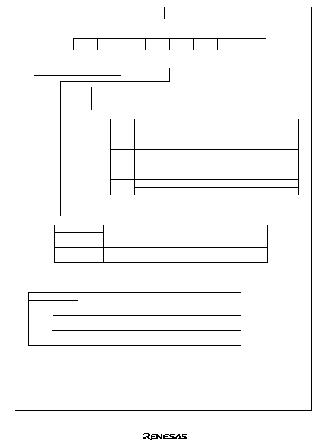
846
16TCR0--Timer Control Register
H'FFF68
16-bit timer channel 0
Bit
Initial value
Read/Write
1
--
7
--
0
R/W
6
CCLR1
0
R/W
5
CCLR0
0
R/W
4
CKEG1
0
R/W
3
CKEG0
0
R/W
2
TPSC2
0
R/W
1
TPSC1
0
R/W
0
TPSC0
Timer prescaler 2 to 0
TCNT Clock Source
Bit 2
TPSC2
Bit 1
TPSC1
Bit 0
TPSC0
Internal clock : �
(Initial value)
Internal clock : � / 2
Internal clock : � / 4
Internal clock : � / 8
External clock A : TCLKA input
External clock B : TCLKB input
External clock C : TCLKC input
External clock D : TCLKD input
0
1
0
1
0
1
0
1
0
1
0
1
0
1
Clock edge 1 and 0
Counted Edges of External Clock
Bit 4
CKEG1
Bit 3
CKEG0
Rising edges counted
Falling edges counted
Both edges counted
0
1
--
0
0
1
Counter clear 1 and 0
TCNT clear Sources
Bit 6
CCLR1
Bit 5
CCLR0
TCNT is not cleared
TCNT is cleared by GRA compare match or input capture
TCNT is cleared by GRB compare match or input capture
Synchronous clear : TCNT is cleared in synchronization with other
synchronized timers
0
1
0
1
0
1
(Initial value)
(Initial value)
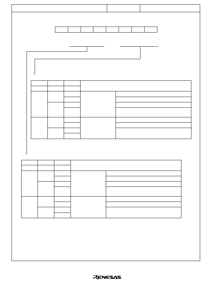
847
TIOR0--Timer I/O Control Register 0
H'FFF69
16-bit timer channel 0
I/O control A2 to A0
GRA Functions
Bit 2
IOA2
Bit 1
IOA1
Bit 0
IOA0
--
1
--
7
IOB2
0
R/W
6
IOB1
0
R/W
5
IOB0
0
R/W
4
--
1
--
3
IOA2
0
R/W
2
IOA1
0
R/W
1
IOA0
0
R/W
0
Bit:
Initial value:
Read/Write:
No output at compare match (Initial value)
0 output at GRA compare match
1 output at GRA compare match
Output toggles at GRA compare match
(channel 2 only: 1 output)
GRA captures rising edges of input
GRA captures falling edges of input
GRA captures both edges of input
0
1
0
1
0
1
0
1
0
1
0
1
0
1
GRA is an output
compare register
GRA is an input
capture register
I/O control B2 to B0
GRB Functions
Bit 6
IOB2
Bit 5
IOB1
Bit 4
IOB0
No output at compare match (Initial value)
0 output at GRB compare match
1 output at GRB compare match
Output toggles at GRB compare match
(channel 2 only: 1 output)
GRB captures rising edges of input
GRB captures falling edges of input
GRB captures both edges of input
0
1
0
1
0
1
0
1
0
1
0
1
0
1
GRB is an output
compare register
GRB is an input
capture register
848
16TCNT0 H/L--Timer Counter 0 H/L
H'FFF6A, H'FFF6B
16-bit timer channel 0
Bit
Initial value
Read/Write
0
R/W
0
R/W
0
R/W
0
R/W
0
R/W
0
R/W
0
R/W
0
R/W
15
14
13
12
11
10
9
8
7
6
5
4
3
2
1
0
0
R/W
0
R/W
0
R/W
0
R/W
0
R/W
0
R/W
0
R/W
0
R/W
Up - counter
GRA0 H/L--General Register A0 H/L
H'FFF6C, H'FFF6D
16-bit timer channel 0
Bit
Initial value
Read/Write
1
R/W
1
R/W
1
R/W
1
R/W
1
R/W
1
R/W
1
R/W
1
R/W
15
14
13
12
11
10
9
8
7
6
5
4
3
2
1
0
1
R/W
1
R/W
1
R/W
1
R/W
1
R/W
1
R/W
1
R/W
1
R/W
Output compare or input capture register
GRB0 H/L--General Register B0 H/L
H'FFF6E, H'FFF6F
16-bit timer channel 0
Bit
Initial value
Read/Write
1
R/W
1
R/W
1
R/W
1
R/W
1
R/W
1
R/W
1
R/W
1
R/W
15
14
13
12
11
10
9
8
7
6
5
4
3
2
1
0
1
R/W
1
R/W
1
R/W
1
R/W
1
R/W
1
R/W
1
R/W
1
R/W
Output compare or input capture register
849
16TCR1 Timer Control Register 1
H'FFF70
16-bit timer channel 1
7
--
1
--
Bit
Initial value
Read/Write
6
CCLR1
0
R/W
5
CCLR0
0
R/W
4
CKEG1
0
R/W
3
CKEG0
0
R/W
2
TPSC2
0
R/W
1
TPSC1
0
R/W
0
TPSC0
0
R/W
Note: Bit functions are the same as for 16-bit timer channel 0.
TIOR1--Timer I/O Control Register 1
H'FFF71
16-bit timer channel 1
7
--
1
--
Bit
Initial value
Read/Write
6
IOB2
0
R/W
5
IOB1
0
R/W
4
IOB0
0
R/W
3
--
1
--
2
IOA2
0
R/W
1
IOA1
0
R/W
0
IOA0
0
R/W
Note: Bit functions are the same as for 16-bit timer channel 0.
16TCNT1 H/L--Timer Counter 1 H/L
H'FFF72, H'FFF73
16-bit timer channel 1
Bit
Initial value
Read/Write
0
R/W
0
R/W
0
R/W
0
R/W
0
R/W
0
R/W
0
R/W
0
R/W
15
14
13
12
11
10
9
8
7
6
5
4
3
2
1
0
0
R/W
0
R/W
0
R/W
0
R/W
0
R/W
0
R/W
0
R/W
0
R/W
Note: Bit functions are the same as for 16-bit timer channel 0.
850
GRA1 H/L--General Register A1 H/L
H'FFF74, H'FFF75
16-bit timer channel 1
Bit
Initial value
Read/Write
1
R/W
1
R/W
1
R/W
1
R/W
1
R/W
1
R/W
1
R/W
1
R/W
15
14
13
12
11
10
9
8
7
6
5
4
3
2
1
0
1
R/W
1
R/W
1
R/W
1
R/W
1
R/W
1
R/W
1
R/W
1
R/W
Note: Bit functions are the same as for 16-bit timer channel 0.
GRB1 H/L--General Register B1 H/L
H'FFF76, H'FFF77
16-bit timer channel 1
Bit
Initial value
Read/Write
1
R/W
1
R/W
1
R/W
1
R/W
1
R/W
1
R/W
1
R/W
1
R/W
15
14
13
12
11
10
9
8
7
6
5
4
3
2
1
0
1
R/W
1
R/W
1
R/W
1
R/W
1
R/W
1
R/W
1
R/W
1
R/W
Note: Bit functions are the same as for 16-bit timer channel 0.
16TCR2 Timer Control Register 2
H'FFF78
16-bit timer channel 2
7
--
1
--
Bit
Initial value
Read/Write
6
CCLR1
0
R/W
5
CCLR0
0
R/W
4
CKEG1
0
R/W
3
CKEG0
0
R/W
2
TPSC2
0
R/W
1
TPSC1
0
R/W
0
TPSC0
0
R/W
Notes : 1. Bit functions are the same as for 16-bit timer channel 0.
2. When phase counting mode is selected in channel 2, the settings of
bits CKEG1 and CKEG0 and TPSC2 to TPSC0 in TCR2 are ignored.
851
TIOR2--Timer I/O Control Register 2
H'FFF79
16-bit timer channel 2
7
--
1
--
Bit
Initial value
Read/Write
6
IOB2
0
R/W
5
IOB1
0
R/W
4
IOB0
0
R/W
3
--
1
--
2
IOA2
0
R/W
1
IOA1
0
R/W
0
IOA0
0
R/W
Note: Bit functions are the same as for 16-bit timer channel 0.
16TCNT2 H/L--Timer Counter 2 H/L
H'FFF7A, H'FFF7B
16-bit timer channel 2
Bit
Initial value
Read/Write
0
R/W
0
R/W
0
R/W
0
R/W
0
R/W
0
R/W
0
R/W
0
R/W
15
14
13
12
11
10
9
8
7
6
5
4
3
2
1
0
0
R/W
0
R/W
0
R/W
0
R/W
0
R/W
0
R/W
0
R/W
0
R/W
Phase counting mode :
Other mode :
up/down counter
up-counter
GRA2 H/L--General Register A2 H/L
H'FFF7C, H'FFF7D
16-bit timer channel 2
Bit
Initial value
Read/Write
1
R/W
1
R/W
1
R/W
1
R/W
1
R/W
1
R/W
1
R/W
1
R/W
15
14
13
12
11
10
9
8
7
6
5
4
3
2
1
0
1
R/W
1
R/W
1
R/W
1
R/W
1
R/W
1
R/W
1
R/W
1
R/W
Note: Bit functions are the same as for 16-bit timer channel 0.

852
GRB2 H/L--General Register B2 H/L
H'FFF7E, H'FFF7F
16-bit timer channel 2
Bit
Initial value
Read/Write
1
R/W
1
R/W
1
R/W
1
R/W
1
R/W
1
R/W
1
R/W
1
R/W
15
14
13
12
11
10
9
8
7
6
5
4
3
2
1
0
1
R/W
1
R/W
1
R/W
1
R/W
1
R/W
1
R/W
1
R/W
1
R/W
Note: Bit functions are the same as for 16-bit timer channel 0.
853
8TCR0--Timer Control Register 0
8TCR1--Timer Control Register 1
H'FFF80
H'FFF81
8-bit timer channel 0
8-bit timer channel 1
Bit
Initial value
Read/Write
0
R/W
7
CMIEB
0
R/W
6
CMIEA
0
R/W
5
OVIE
0
R/W
4
CCLR1
0
R/W
3
CCLR0
0
R/W
2
CKS2
0
R/W
1
CKS1
0
R/W
0
CKS0
Clock select 2 to 0
0
0
0
1
0
1
0
0
1
1
0
1
1
Clock input is disabled
Internal clock, counted on rising
edge of
/8
Internal clock, counted on rising
edge of
/64
Internal clock, counted on rising
edge of
/8192
External clock, counted on falling edge
External clock, counted on rising edge
External clock, counted on both
rising and falling edges
Counter clear 1 and 0
0
0
1
0
1
Clearing is disabled
Cleared by compare match A
Cleared by compare match B/input capture B
Cleared by input capture B
1
Timer overflow interrupt enable
0
1
OVI interrupt requested by OVF is disabled
OVI interrupt requested by OVF is enabled
Compare match interrupt enable A
0
1
CMIA interrupt requested by CMFA is disabled
CMIA interrupt requested by CMFA is enabled
Compare match interrupt enable B
0
1
CMIB interrupt requested by CMFB is disabled
CMIB interrupt requested by CMFB is enabled
1
Channel 0:
Count on TCNT1 overflow signal
*
Channel 1:
Count on TCNT0 compare match
A
*
Notes:
*
If the clock input of channel 0 is the TCNT1
overflow signal and that of channel 1 is the
TCNT0 compare match signal, no
incrementing clock is generated. Do not use
this setting.
854
8TCSR0--Timer Control/Status Register 0
H'FFF82
8-bit timer channel 0
Output select A1 and A0
0
Description
Description
Description
Bit 1
OS1
Bit 0
OS0
ICE in
TCSR1
Bit 3
OIS3
Bit 4
ADTE
TRGE
*
1
Bit 2
OIS2
1
0
1
No change at compare match A
0 output at compare match A
1 output at compare match A
Output toggles at compare
match A
Output/input capture edge select B3 and B2
0
0
1
0
1
0
1
0
1
0
1
0
1
No change at compare match B
0 output at compare match B
1 output at compare match B
Output toggles at compare match
B
TCORB input capture on rising
edge
TCORB input capture on falling
edge
TCORB input capture on both
rising and falling edges
1
A/D trigger enable (TCSR0 only)
0
0
1
0
1
A/D converter start requests by compare match A
or an external trigger are disabled
A/D converter start requests by compare match A
or an external trigger are enabled
A/D converter start requests by an external trigger are enabled
A/D converter start requests by compare match A are enabled
Timer overflow flag
0
[Clearing condition]
Read OVF when OVF = 1, then write 0 in OVF
Bit
Initial value
Read/Write
0
R/(W)
*
7
CMFB
0
R/(W)
*
6
CMFA
0
R/(W)
*
5
OVF
0
R/W
4
ADTE
0
R/W
3
OIS3
0
R/W
2
OIS2
0
R/W
1
OS1
0
R/W
0
OS0
0
1
1
[Setting condition]
TCNT overflows from H'FF to H'00
Compare match flag A
0
[Clearing condition]
Read CMFA when CMFA = 1, then write 0 in CMFA
1
[Setting condition]
TCNT = TCORA
Compare match/input capture flag B
0
[Clearing condition]
Read CMFB when CMFB = 1, then write 0 in CMFB
1
[Setting conditions]
TCNT = TCORB
The TCNT value is transferred to TCORB by an input capture signal when
TCORB functions as an input capture register.
Note:
*
Only 0 can be written to bits 7 to 5, to clear these flags.
Note:
*
1 TRGE is bit 7 of the A/D control register (ADCR).
1
855
8TCSR1--Timer Control/Status Register 1
H'FFF83
8-bit timer channel 1
Output select A1 and A0
0
Description
Description
Bit 1
OS1
Bit 0
OS0
ICE in
TCSR1
Bit 3
OIS3
Bit 2
OIS2
1
0
1
No change at compare match A
0 output at compare match A
1 output at compare match A
Output toggles at compare
match A
Output/input capture edge select B3 and B2
0
0
1
0
1
0
1
0
1
0
1
0
1
No change at compare match B
0 output at compare match B
1 output at compare match B
Output toggles at compare match
B
TCORB input capture on rising
edge
TCORB input capture on falling
edge
TCORB input capture on both
rising and falling edges
1
Timer overflow flag
0
[Clearing condition]
Read OVF when OVF = 1, then write 0 in OVF
0
1
1
[Setting condition]
TCNT overflows from H'FF to H'00
Compare match flag A
0
[Clearing condition]
Read CMFA when CMFA = 1, then write 0 in CMFA
1
[Setting condition]
TCNT = TCORA
Compare match/input capture flag B
0
[Clearing condition]
Read CMFB when CMFB = 1, then write 0 in CMFB
1
[Setting conditions]
TCNT = TCORB
The TCNT value is transferred to TCORB by an input capture signal when
TCORB functions as an input capture register.
Note:
*
Only 0 can be written to bits 7 to 5, to clear these flags.
Bit
Initial value
Read/Write
0
R/(W)
*
7
CMFB
0
R/(W)
*
6
CMFA
0
R/(W)
*
5
OVF
0
R/W
4
ICE
0
R/W
3
OIS3
0
R/W
2
OIS2
0
R/W
1
OS1
0
R/W
0
OS0
Input capture enable
0
1
TCORB is a compare match register
TCORB is an input capture register
856
TCORA0--Time Constant Register A0
TCORA1--Time Constant Register A1
H'FFF84
H'FFF85
8-bit timer channel 0
8-bit timer channel 1
Bit
Initial value
Read/Write
1
R/W
1
R/W
1
R/W
1
R/W
1
R/W
1
R/W
1
R/W
1
R/W
15
14
13
12
11
10
9
8
7
6
5
4
3
2
1
0
1
R/W
1
R/W
1
R/W
1
R/W
1
R/W
1
R/W
1
R/W
1
R/W
TCORA0
TCORA1
TCORB0--Time Constant Register B0
TCORB1--Time Constant Register B1
H'FFF86
H'FFF87
8-bit timer channel 0
8-bit timer channel 1
Bit
Initial value
Read/Write
1
R/W
1
R/W
1
R/W
1
R/W
1
R/W
1
R/W
1
R/W
1
R/W
15
14
13
12
11
10
9
8
7
6
5
4
3
2
1
0
1
R/W
1
R/W
1
R/W
1
R/W
1
R/W
1
R/W
1
R/W
1
R/W
TCORB0
TCORB1
8TCNT0--Timer Counter 0
8TCNT1--Timer Counter 1
H'FFF88
H'FFF89
8-bit timer channel 0
8-bit timer channel 1
Bit
Initial value
Read/Write
0
R/W
0
R/W
0
R/W
0
R/W
0
R/W
0
R/W
0
R/W
0
R/W
15
14
13
12
11
10
9
8
7
6
5
4
3
2
1
0
0
R/W
0
R/W
0
R/W
0
R/W
0
R/W
0
R/W
0
R/W
0
R/W
TCNT0
TCNT1
857
TCSR--Timer Control/Status Register
H'FFF8C
WDT
Bit
Initial value
Read/Write
0
R/(W)
*
7
OVF
0
R/W
6
WT/
IT
0
R/W
5
TME
4
1
1
3
0
R/W
2
CKS2
0
R/W
1
CKS1
Clock select 2 to 0
0
0
/2
/32
/64
/128
/256
/512
/2048
/4096
1
0
CKS0
0
R/W
0
1
0
1
0
1
0
1
1
0
1
Timer enable
0
Timer disabled
� TCNT is initialized to H'00 and
halted
1
Timer enabled
� TCNT is counting
Timer mode select
0
Interval timer:
requests interval timer interrupts
1
Watchdog timer:
generates a reset signal
Overflow flag
0
[Clearing condition]
Read OVF when OVF = 1, then write 0 in OVF
1
[Setting condition]
TCNT changes from H'FF to H'00
Note:
*
Only 0 can be written, to clear the flag.
CKS2 CKS1 CKS0
Description
858
TCNT--Timer Counter
H'FFF8D (read), H'FFF8C (write)
WDT
Bit
Initial value
Read/Write
0
R/W
7
0
R/W
6
0
R/W
5
0
R/W
4
0
R/W
3
0
R/W
2
0
R/W
1
0
R/W
0
Count value
RSTCSR--Reset Control/Status Register
H'FFF8F (read), H'FFF8E (write)
WDT
Bit
Initial value
Read/Write
0
R/(W)
*
7
WRST
0
R/W
6
1
5
1
4
1
3
1
2
1
1
1
0
Reserved bits
Watchdog timer reset
0
[Clearing conditions]
Reset signal at
RES
pin
Read WRST when WRST = 1, then write 0 in WRST
1
[Setting condition]
TCNT overflow generates a reset signal
Note:
*
Only 0 can be written in bit 7, to clear the flag.
859
8TCR2--Timer Control Register 2
8TCR3--Timer Control Register 3
H'FFF90
H'FFF91
8-bit timer channel 2
8-bit timer channel 3
Bit
Initial value
Read/Write
0
R/W
7
CMIEB
0
R/W
6
CMIEA
0
R/W
5
OVIE
0
R/W
4
CCLR1
0
R/W
3
CCLR0
0
R/W
2
CKS2
0
R/W
1
CKS1
0
R/W
0
CKS0
Clock select 2 to 0
0
0
0
1
0
1
0
0
1
1
0
1
1
Clock input is disabled
Internal clock, counted on rising edge
of
/8
Internal clock, counted on rising edge
of
/64
Internal clock, counted on rising edge
of
/8192
External clock, counted on falling edge
External clock, counted on rising edge
External clock, counted on both
rising and falling edges
Counter clear 1 and 0
0
0
1
0
1
Clearing is disabled
Cleared by compare match A
Cleared by compare match B/input capture B
Cleared by input capture B
1
Timer overflow interrupt enable
0
1
OVI interrupt requested by OVF is disabled
OVI interrupt requested by OVF is enabled
Compare match interrupt enable A
0
1
CMIA interrupt requested by CMFA is disabled
CMIA interrupt requested by CMFA is enabled
Compare match interrupt enable B
0
1
CMIB interrupt requested by CMFB is disabled
CMIB interrupt requested by CMFB is enabled
1
CSK2 CSK1 CSK0
Description
Channel 2:
Count on TCNT3 overflow signal
*
Channel 3:
Count on TCNT2 compare match A
*
Note:
*
If the clock input of channel 2 is the TCNT3 overflow
signal and that of channel 3 is the TCNT2 compare
match signal, no incrementing clock is generated. Do
not use this setting.
860
8TCSR2--Timer Control/Status Register 2
8TCSR3--Timer Control/Status Register 3
H'FFF92
H'FFF93
8-bit timer channel 2
8-bit timer channel 3
Bit
Initial value
Read/Write
0
R/(W)
*
7
CMFB
0
R/(W)
*
6
CMFA
0
R/(W)
*
5
OVF
0
R/W
4
ICE
0
R/W
3
OIS3
0
R/W
2
OIS2
0
R/W
1
OS1
0
R/W
0
OS0
Timer overflow flag
0
[Clearing condition]
Read OVF when OVF = 1, then write 0 in OVF
Bit
Initial value
Read/Write
0
R/(W)
*
7
CMFB
0
R/(W)
*
6
CMFA
0
R/(W)
*
5
OVF
1
4
0
R/W
3
OIS3
0
R/W
2
OIS2
0
R/W
1
OS1
0
R/W
0
OS0
TCSR3
TCSR2
1
[Setting condition]
TCNT overflows from H'FF to H'00
Compare match flag A
0
[Clearing condition]
Read CMFA when CMFA = 1, then write 0 in CMFA
1
[Setting condition]
TCNT = TCORA
Compare match/input capture flag B
0
[Clearing condition]
Read CMFB when CMFB = 1, then write 0 in CMFB
1
[Setting conditions]
TCNT = TCORB
The TCNT value is transferred to TCORB by an input capture signal when
TCORB functions as an input capture register.
Note:
*
Only 0 can be written to bits 7 to 5, to clear these flags.
Output select A1 and A0
0
Description
Bit 1
OS1
Bit 0
OS0
1
0
1
No change at compare match A
0 output at compare match A
1 output at compare match A
Output toggles at compare
match A
0
1
Description
ICE in
TCSR3
Bit 3
OIS3
Bit 3
OIS2
Output/input capture edge select B3 and B2
0
0
1
0
1
0
1
0
1
0
1
0
No change at compare match B
0 output at compare match B
1 output at compare match B
Output toggles at compare match
B
TCORB input capture on rising
edge
TCORB input capture on falling
edge
TCORB input capture on both
rising and falling edges
1
Input capture enable (TCSR3 only)
0
1
TCORB is a compare match register
TCORB is an input capture register
861
TCORA2--Time Constant Register A2
TCORA3--Time Constant Register A3
H'FFF94
H'FFF95
8-bit timer channel 2
8-bit timer channel 3
Bit
Initial value
Read/Write
1
R/W
1
R/W
1
R/W
1
R/W
1
R/W
1
R/W
1
R/W
1
R/W
15
14
13
12
11
10
9
8
7
6
5
4
3
2
1
0
1
R/W
1
R/W
1
R/W
1
R/W
1
R/W
1
R/W
1
R/W
1
R/W
TCORA2
TCORA3
TCORB2--Time Constant Register B2
TCORB3--Time Constant Register B3
H'FFF96
H'FFF97
8-bit timer channel 2
8-bit timer channel 3
Bit
Initial value
Read/Write
1
R/W
1
R/W
1
R/W
1
R/W
1
R/W
1
R/W
1
R/W
1
R/W
15
14
13
12
11
10
9
8
7
6
5
4
3
2
1
0
1
R/W
1
R/W
1
R/W
1
R/W
1
R/W
1
R/W
1
R/W
1
R/W
TCORB2
TCORB3
8TCNT2--Timer Counter 2
8TCNT3--Timer Counter 3
H'FFF98
H'FFF99
8-bit timer channel 2
8-bit timer channel 3
Bit
Initial value
Read/Write
0
R/W
0
R/W
0
R/W
0
R/W
0
R/W
0
R/W
0
R/W
0
R/W
15
14
13
12
11
10
9
8
7
6
5
4
3
2
1
0
0
R/W
0
R/W
0
R/W
0
R/W
0
R/W
0
R/W
0
R/W
0
R/W
TCNT2
TCNT3
862
DADR0--D/A Data Register 0
H'FFF9C
D/A
Bit
Initial value
Read/Write
0
R/W
7
0
R/W
6
0
R/W
5
0
R/W
4
0
R/W
3
0
R/W
2
0
R/W
1
0
R/W
0
D/A conversion data
DADR1--D/A Data Register 1
H'FFF9D
D/A
Bit
Initial value
Read/Write
0
R/W
7
0
R/W
6
0
R/W
5
0
R/W
4
0
R/W
3
0
R/W
2
0
R/W
1
0
R/W
0
D/A conversion data
863
DACR--D/A Control Register
H'FFF9E
D/A
Bit
Initial value
Read/Write
0
R/W
7
DAOE1
0
R/W
6
DAOE0
0
R/W
5
DAE
1
4
1
3
1
2
1
1
1
0
D/A enable
Bit 7
DAOE1
D/A conversion is disabled
in channels 0 and 1
D/A conversion is enabled
in channel 0
D/A conversion is disabled
in channel 1
D/A conversion is disabled
in channel 0
D/A conversion is enabled
in channel 1
Description
D/A conversion is enabled
in channels 0 and 1
D/A conversion is enabled
in channels 0 and 1
D/A conversion is enabled
in channels 0 and 1
Bit 6
Bit 5
DAOE0
DAE
0
0
0
1
1
1
0
1
1
0
0
1
0
1
0
1
D/A output enable 0
0
DA
0
analog output is disabled
1
Channel-0 D/A conversion and DA
0
analog output are enabled
D/A output enable 1
0
DA
1
analog output is disabled
1
Channel-1 D/A conversion and DA
1
analog output are enabled
864
TPMR--TPC Output Mode Register
H'FFFA0
TPC
Bit
Initial value
Read/Write
1
7
1
6
1
5
1
4
0
R/W
3
G3NOV
0
R/W
2
G2NOV
0
R/W
1
G1NOV
0
R/W
0
G0NOV
Group 0 non-overlap
0
Normal TPC output in group 0. Output values
change at compare match A in the selected
16-bit timer channel
1
Non-overlapping TPC output in group 0,
controlled by compare match A and B in the
selected 16-bit timer channel
Group 1 non-overlap
0
Normal TPC output in group 1. Output values change
at compare match A in the selected 16-bit timer channel
1
Non-overlapping TPC output in group 1, controlled by
compare match A and B in the selected 16-bit timer channel
Group 2 non-overlap
0
Normal TPC output in group 2. Output values change at
compare match A in the selected 16-bit timer channel
1
Non-overlapping TPC output in group 2, controlled by
compare match A and B in the selected 16-bit timer channel
Group 3 non-overlap
0
Normal TPC output in group 3. Output values change at
compare match A in the selected 16-bit timer channel
1
Non-overlapping TPC output in group 3, controlled by
compare match A and B in the selected 16-bit timer channel
865
TPCR--TPC Output Control Register
H'FFFA1
TPC
Group 0 compare match select 1 and 0
Bit 1
G0CMS1
16-Bit Timer Channel Selected as Output Trigger
Bit 0
G0CMS0
TPC output group 0 (TP
3
to TP
0
) is triggered by
compare match in 16-bit timer channel 0
TPC output group 0 (TP
3
to TP
0
) is triggered by
compare match in 16-bit timer channel 1
TPC output group 0 (TP
3
to TP
0
) is triggered by
compare match in 16-bit timer channel 2
0
1
0
1
0
1
Group 1 compare match select 1 and 0
Bit 3
G1CMS1
16-Bit Timer Channel Selected as Output Trigger
Bit 2
G1CMS0
TPC output group 1 (TP
7
to TP
4
) is triggered by
compare match in 16-bit timer channel 0
TPC output group 1 (TP
7
to TP
4
) is triggered by
compare match in 16-bit timer channel 1
TPC output group 1 (TP
7
to TP
4
) is triggered by
compare match in 16-bit timer channel 2
0
1
0
1
0
1
Group 2 compare match select 1 and 0
Bit 5
G2CMS1
16-Bit Timer Channel Selected as Output Trigger
Bit 4
G2CMS0
TPC output group 2 (TP
11
to TP
8
) is triggered by compare match in 16-bit timer channel 0
TPC output group 2 (TP
11
to TP
8
) is triggered by compare match in 16-bit timer channel 1
TPC output group 2 (TP
11
to TP
8
) is triggered by compare match in 16-bit timer channel 2
0
1
0
1
0
1
Group 3 compare match select 1 and 0
Bit 7
G3CMS1
16-Bit Timer Channel Selected as Output Trigger
Bit 6
G3CMS0
TPC output group 3 (TP
15
to TP
12
) is triggered by compare match in 16-bit timer channel 0
TPC output group 3 (TP
15
to TP
12
) is triggered by compare match in 16-bit timer channel 1
TPC output group 3 (TP
15
to TP
12
) is triggered by compare match in 16-bit timer channel 2
0
1
0
1
0
1
Bit
Initial value
Read/Write
7
G3CMS1
6
G3CMS0
5
G2CMS1
4
G2CMS0
1
R/W
3
G1CMS1
1
R/W
2
G1CMS0
1
R/W
1
G0CMS1
1
R/W
0
G0CMS0
1
R/W
1
R/W
1
R/W
1
R/W
866
NDERB--Next Data Enable Register B
H'FFFA2
TPC
Bit
Initial value
Read/Write
0
R/W
7
NDER15
0
R/W
6
NDER14
0
R/W
5
NDER13
0
R/W
4
NDER12
0
R/W
3
NDER11
0
R/W
2
NDER10
0
R/W
1
NDER9
0
R/W
0
NDER8
Next data enable 15 to 8
Bits 7 to 0
NDER15
to NDER8
Description
TPC outputs TP
15
to TP
8
are disabled
(NDR15 to NDR8 are not transferred to PB
7
to PB
0
)
TPC outputs TP
15
to TP
8
are enabled
(NDR15 to NDR8 are transferred to PB
7
to PB
0
)
0
1
NDERA--Next Data Enable Register A
H'FFFA3
TPC
Bit
Initial value
Read/Write
0
R/W
7
NDER7
0
R/W
6
NDER6
0
R/W
5
NDER5
0
R/W
4
NDER4
0
R/W
3
NDER3
0
R/W
2
NDER2
0
R/W
1
NDER1
0
R/W
0
NDER0
Next data enable 7 to 0
Bits 7 to 0
NDER7
to NDER0
Description
TPC outputs TP
7
to TP
0
are disabled
(NDR7 to NDR0 are not transferred to PA
7
to PA
0
)
TPC outputs TP
7
to TP
0
are enabled
(NDR7 to NDR0 are transferred to PA
7
to PA
0
)
0
1
867
NDRB--Next Data Register B
H'FFFA4/H'FFFA6
TPC
�
Same trigger for TPC output groups 2 and 3
Address H'FFFA4
Bit
Initial value
Read/Write
0
R/W
7
NDR15
0
R/W
6
NDR14
0
R/W
5
NDR13
0
R/W
4
NDR12
0
R/W
3
NDR11
0
R/W
2
NDR10
0
R/W
1
NDR9
0
R/W
0
NDR8
Store the next output data for TPC output group 3
Store the next output data for TPC output group 2
Address H'FFFA6
1
7
1
6
1
5
1
4
1
3
1
2
1
1
1
0
Bit
Initial value
Read/Write
�
Different triggers for TPC output groups 2 and 3
Address H'FFFA4
Bit
Initial value
Read/Write
0
R/W
7
NDR15
0
R/W
6
NDR14
0
R/W
5
NDR13
0
R/W
4
NDR12
1
3
1
2
1
1
1
0
Store the next output data for TPC output group 3
Address H'FFFA6
Bit
Initial value
Read/Write
0
R/W
7
0
R/W
6
0
R/W
5
0
R/W
4
3
NDR11
2
NDR10
1
NDR9
1
1
1
1
0
NDR8
Store the next output data for TPC output group 2
868
NDRA--Next Data Register A
H'FFFA5/H'FFFA7
TPC
�
Same trigger for TPC output groups 0 and 1
Address H'FFFA5
Bit
Initial value
Read/Write
0
R/W
7
NDR7
0
R/W
6
NDR6
0
R/W
5
NDR5
0
R/W
4
NDR4
0
R/W
3
NDR3
0
R/W
2
NDR2
0
R/W
1
NDR1
0
R/W
0
NDR0
Store the next output data for TPC output group 1
Store the next output data for TPC output group 0
Address H'FFFA7
1
7
1
6
1
5
1
4
1
3
1
2
1
1
1
0
Bit
Initial value
Read/Write
�
Different triggers for TPC output groups 0 and 1
Address H'FFFA5
Bit
Initial value
Read/Write
0
R/W
7
NDR7
0
R/W
6
NDR6
0
R/W
5
NDR5
0
R/W
4
NDR4
1
3
1
2
1
1
1
0
Store the next output data for TPC output group 1
Address H'FFFA7
Bit
Initial value
Read/Write
0
R/W
7
0
R/W
6
0
R/W
5
0
R/W
4
3
NDR3
2
NDR2
1
NDR1
1
1
1
1
0
NDR0
Store the next output data for TPC output group 0
869
SMR--Serial Mode Register
H'FFFB0
SCI0
Bit
Initial value
Read/Write
0
R/W
7
C/
A
0
R/W
6
CHR
0
R/W
5
PE
4
O/
E
0
R/W
0
R/W
3
STOP
0
R/W
2
MP
0
R/W
1
CKS1
Clock select 1 and 0
0
Bit 0
clock
/4 clock
/16 clock
/64 clock
1
0
CKS0
0
R/W
Multiprocessor mode
0
Multiprocessor function disabled
Multiprocessor format selected
1
Bit 1
Clock Source
CKS0
CKS1
0
1
0
1
Stop bit length
0
One stop bit
Two stop bits
1
Parity mode
0
Even parity
Odd parity
1
Parity enable
0
Parity bit is not added or checked
Parity bit is added and checked
1
GSM mode (for smart card interface)
0
TEND flag is set 12.5 etu
*
after start bit
TEND flag is set 11.0 etu
*
after start bit
1
Character length
0
8-bit data
7-bit data
1
Communication mode (for serial communication interface)
0
Asynchronous mode
Synchronous mode
1
Note:
*
etu: Elementary time unit (time required to transmit one bit)

870
BRR--Bit Rate Register
H'FFFB1
SCI0
Bit
Initial value
Read/Write
1
R/W
7
1
R/W
6
1
R/W
5
1
R/W
4
1
R/W
3
1
R/W
2
1
R/W
1
1
R/W
0
Serial communication bit rate setting
871
SCR--Serial Control Register
H'FFFB2
SCI0
Bit
Initial value
Read/Write
0
R/W
7
TIE
0
R/W
6
RIE
0
R/W
5
TE
0
R/W
4
RE
0
R/W
3
MPIE
0
R/W
2
TEIE
0
R/W
1
CKE1
0
R/W
0
CKE0
Clock enable 1 and 0
(for serial communication interface)
Bit 1
CKE1
Bit 0
CKE0
Asynchronous mode
Synchronous mode
Asynchronous mode
Synchronous mode
Asynchronous mode
Synchronous mode
Asynchronous mode
Synchronous mode
0
1
0
1
0
1
Description
Transmit-end interrupt enable
0
1
Transmit-end interrupt requests (TEI) are disabled
Transmit-end interrupt requests (TEI) are enabled
Receive interrupt enable
0
1
Receive-data-full (RXI) and receive-error (ERI) interrupt requests are disabled
Receive-data-full (RXI) and receive-error (ERI) interrupt requests are enabled
Internal clock, SCK pin
available for generic I/O
Internal clock, SCK pin
used for serial clock output
Internal clock, SCK pin
used for clock output
Internal clock, SCK pin
used for serial clock output
External clock, SCK pin
used for clock input
External clock, SCK pin
used for serial clock input
External clock, SCK pin
used for clock input
External clock, SCK pin
used for serial clock input
Multiprocessor interrupt enable
0
1
Multiprocessor interrupts are disabled (normal receive operation)
Multiprocessor interrupts are enabled
Receive enable
0
1
Receiving is
disabled
Receiving is
enabled
Transmit enable
0
1
Transmitting is disabled
Transmitting is enabled
Transmit interrupt enable
0
1
Transmit-data-empty interrupt request (TXI) is disabled
Transmit-data-empty interrupt request (TXI) is enabled
Clock enable 1 and 0 (for smart card interface)
SMR
GM
Bit 1
CKE1
Bit 0
CKE0
0
0
1
0
1
0
1
0
1
0
1
Description
SCK pin available for generic I/O
SCK pin used for clock output
SCK pin output fixed low
SCK pin used for clock output
SCK pin output fixed high
SCK pin used for clock output

872
TDR--Transmit Data Register
H'FFFB3
SCI0
Bit
Initial value
Read/Write
1
R/W
7
1
R/W
6
1
R/W
5
1
R/W
4
1
R/W
3
1
R/W
2
1
R/W
1
1
R/W
0
Serial transmit data
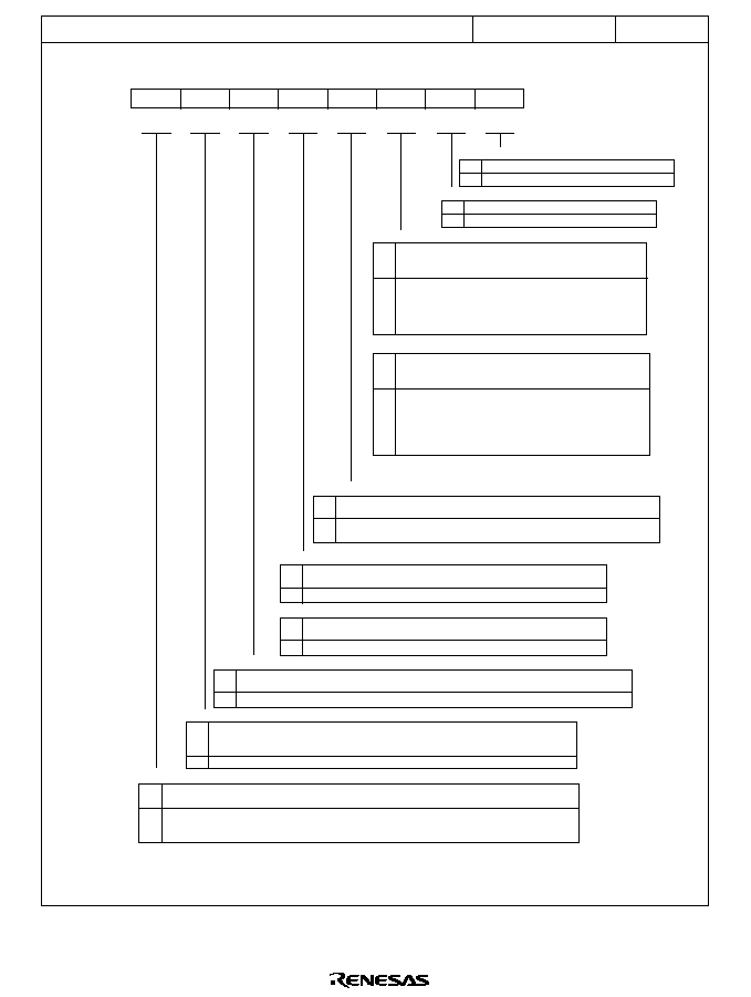
873
SSR--Serial Status Register
H'FFFB4
SCI0
Bit
Initial value
Read/Write
1
R/(W)
*
7
TDRE
0
R/(W)
*
6
RDRF
0
R/(W)
*
5
ORER
0
R/(W)
*
4
FER/ERS
0
R/(W)
*
3
PER
1
R
2
TEND
0
R
1
MPB
0
R/W
0
MPBT
Transmit end (for serial communication interface)
0
Multiprocessor bit transfer
0
1
Multiprocessor bit value in transmit data is 0
Multiprocessor bit value in transmit data is 1
Multiprocessor bit
0
1
Multiprocessor bit value in receive data is 0
Multiprocessor bit value in receive data is 1
[Clearing conditions]
Read TDRE when TDRE = 1, then write 0 in TDRE.
The DMAC writes data in TDR.
[Setting conditions]
Reset or transition to standby mode
TE is cleared to 0 in SCR.
TDRE is 1 when last bit of 1-byte serial character is
transmitted.
Parity error
0
1
[Clearing conditions] Reset or transition to standby mode.
Read PER when PER = 1, then write 0 in PER
[Setting condition]
Parity error (parity of receive data does not match parity
setting of O/
E
bit in SMR)
Framing error (for serial communication interface)
0
[Clearing conditions]
Reset or transition to standby mode.
Read FER when FER = 1, then write 0 in FER
[Setting condition]
Framing error (stop bit is 0)
Error signal status (for smart card interface)
0
[Clearing conditions]
Reset or transition to standby mode.
Read ERS when ERS = 1, then write 0 in ERS
[Setting condition]
A low error signal is received
1
1
Overrun error
0
[Clearing conditions]
Reset or transition to standby mode.
Read ORER when ORER = 1, then write 0 in ORER
[Setting condition]
Overrun error (reception of the next serial data ends when RDRF = 1)
1
Receive data register full
0
[Clearing conditions]
Reset or transition to standby mode.
Read RDRF when RDRF = 1, then write 0 in RDRF
The DMAC reads data from RDR
[Setting condition]
Serial data is received normally and transferred from RSR to RDR
1
Transmit data register empty
Note:
*
Only 0 can be written, to clear the flag.
0
[Clearing conditions] Read TDRE when TDRE = 1, then write 0 in TDRE
The DMAC writes data in TDR
[Setting conditions]
Reset or transition to standby mode.
TE is 0 in SCR
Data is transferred from TDR to TSR, enabling new data to be written in TDR.
1
1
Transmit end (for smart card interface)
0
[Clearing conditions]
Read TDRE when TDRE = 1, then write 0 in TDRE.
The DMAC writes data in TDR.
[Setting conditions]
Reset or transition to standby mode
TE is cleared to 0 in SCR and FER/ERS is cleared to 0.
TDRE is 1 and FER/ERS is 0 (normal transmission) 2.5 etu
*
1
(when GM = 0) or 1.0 etu (when GM = 1) after 1-byte serial
character is transmitted.
1
Note:
*
1 etu: Elementary time unit (time required to transmit one bit)

874
RDR--Receive Data Register
H'FFFB5
SCI0
Bit
Initial value
Read/Write
0
R
7
0
R
6
0
R
5
0
R
4
0
R
3
0
R
2
0
R
1
0
R
0
Serial receive data
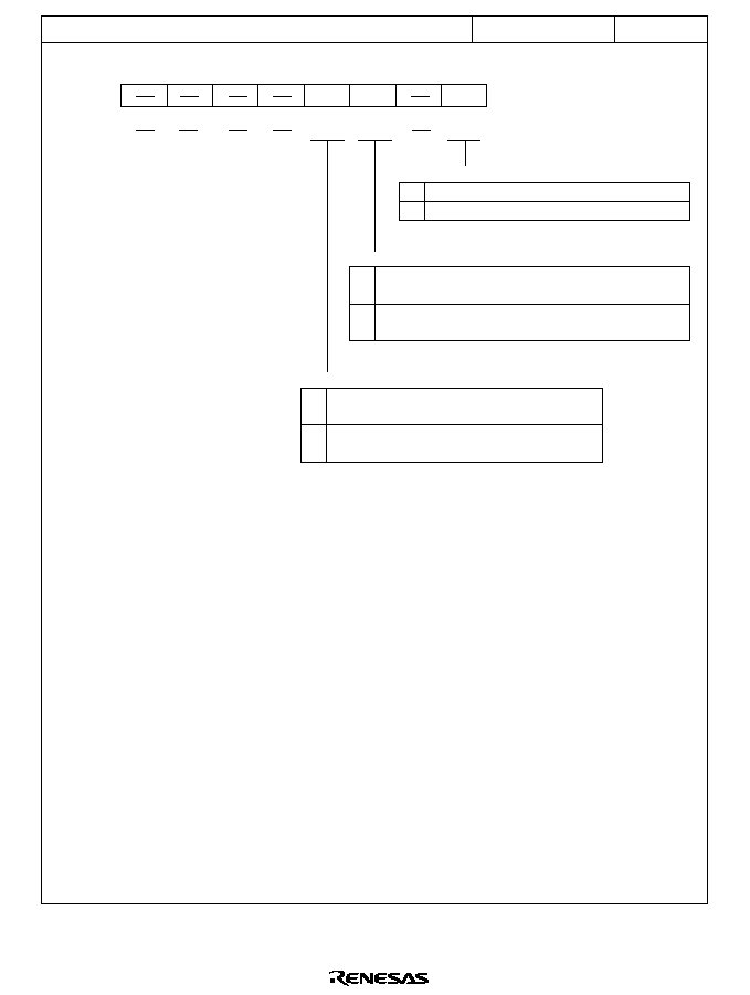
875
SCMR--Smart Card Mode Register
H'FFFB6
SCI0
1
7
1
6
1
5
1
4
0
R/W
3
SDIR
0
R/W
2
SINV
1
1
0
R/W
0
SMIF
Smart card interface mode select
0
1
Smart card interface function is disabled
(Initial value)
Smart card interface function is enabled
Smart card data invert
0
1
Unmodified TDR contents are transmitted
(Initial value)
Receive data is stored unmodified in RDR
Inverted 1/0 logic levels of TDR contents are transmitted
1/0 logic levels of received data are inverted before storage in RDR
Smart card data transfer direction
0
1
TDR contents are transmitted LSB-first
(Initial value)
Receive data is stored LSB-first in RDR
TDR contents are transmitted MSB-first
Receive data is stored MSB-first in RDR
Bit
Initial value
Read/Write
876
SMR--Serial Mode Register
H'FFFB8
SCI1
0
R/W
7
C/
A
0
R/W
6
CHR
0
R/W
5
PE
0
R/W
4
O/
E
0
R/W
3
STOP
0
R/W
2
MP
0
R/W
1
CKS1
0
R/W
0
CKS0
Note: Bit functions are the same as for SCI0.
Bit
Initial value
Read/Write
BRR--Bit Rate Register
H'FFFB9
SCI1
1
R/W
7
1
R/W
6
1
R/W
5
1
R/W
4
1
R/W
3
1
R/W
2
1
R/W
1
1
R/W
0
Note: Bit functions are the same as for SCI0.
Bit
Initial value
Read/Write
SCR--Serial Control Register
H'FFFBA
SCI1
0
R/W
7
TIE
0
R/W
6
RIE
0
R/W
5
TE
0
R/W
4
RE
0
R/W
3
MPIE
0
R/W
2
TEIE
0
R/W
1
CKE1
0
R/W
0
CKE0
Note: Bit functions are the same as for SCI0.
Bit
Initial value
Read/Write
877
TDR--Transmit Data Register
H'FFFBB
SCI1
1
R/W
7
1
R/W
6
1
R/W
5
1
R/W
4
1
R/W
3
1
R/W
2
1
R/W
1
1
R/W
0
Bit
Initial value
Read/Write
Note: Bit functions are the same as for SCI0.
SSR--Serial Status Register
H'FFFBC
SCI1
0
R/(W)
*
7
TDRE
0
R/(W)
*
6
RDRF
0
R/(W)
*
5
ORER
0
R/(W)
*
4
FER/ERS
0
R/(W)
*
3
PER
1
R
2
TEND
0
R
1
MPB
0
R/W
0
MPBT
Bit
Initial value
Read/Write
Notes: Bit functions are the same as for SCI0.
*
Only 0 can be written, to clear the flag.
RDR--Receive Data Register
H'FFFBD
SCI1
0
R
7
0
R
6
0
R
5
0
R
4
0
R
3
0
R
2
0
R
1
0
R
0
Bit
Initial value
Read/Write
Note: Bit functions are the same as for SCI0.

878
SCMR--Smart Card Mode Register
H'FFFBE
SCI1
0
R/W
7
0
R/W
6
1
5
0
R/W
4
3
SDIR
2
SINV
1
1
1
1
1
0
SMIF
Bit
Initial value
Read/Write
Note: Bit functions are the same as for SCI0.

879
SMR--Serial Mode Register
H'FFFC0
SCI2
0
R/W
7
C/
A
0
R/W
6
CHR
0
R/W
5
PE
0
R/W
4
O/
E
0
R/W
3
STOP
0
R/W
2
MP
0
R/W
1
CKS1
0
R/W
0
CKS0
Bit
Initial value
Read/Write
Note: Bit functions are the same as for SCI0.
BRR--Bit Rate Register
H'FFFC1
SCI2
1
R/W
7
1
R/W
6
1
R/W
5
1
R/W
4
1
R/W
3
1
R/W
2
1
R/W
1
1
R/W
0
Bit
Initial value
Read/Write
Note: Bit functions are the same as for SCI0.
SCR--Serial Control Register
H'FFFC2
SCI2
0
R/W
7
TIE
0
R/W
6
RIE
0
R/W
5
TE
0
R/W
4
RE
0
R/W
3
MPIE
0
R/W
2
TEIE
0
R/W
1
CKE1
0
R/W
0
CKE0
Bit
Initial value
Read/Write
Note: Bit functions are the same as for SCI0.
880
TDR--Transmit Data Register
H'FFFC3
SCI2
1
R/W
7
1
R/W
6
1
R/W
5
1
R/W
4
1
R/W
3
1
R/W
2
1
R/W
1
1
R/W
0
Bit
Initial value
Read/Write
Note: Bit functions are the same as for SCI0.
SSR--Serial Status Register
H'FFFC4
SCI2
1
R/(W)
*
7
TDRE
0
R/(W)
*
6
RDRF
0
R/(W)
*
5
ORER
0
R/(W)
*
4
FER/ERS
0
R/(W)
*
3
PER
1
R
2
TEND
0
R
1
MPB
0
R/W
0
MPBT
Bit
Initial value
Read/Write
Notes: Bit functions are the same as for SCI0.
*
Only 0 can be written, to clear the flag.
RDR--Receive Data Register
H'FFFC5
SCI2
0
R
7
0
R
6
0
R
5
0
R
4
0
R
3
0
R
2
0
R
1
0
R
0
Bit
Initial value
Read/Write
Note: Bit functions are the same as for SCI0.

881
SCMR--Smart Card Mode Register
H'FFFC6
SCI2
0
R/W
7
0
R/W
6
1
5
0
R/W
4
3
SDIR
2
SINV
1
1
1
1
1
0
SMIF
Bit
Initial value
Read/Write
Note: Bit functions are the same as for SCI0.
882
P1DR--Port 1 Data Register
H'FFFD0
Port 1
0
R/W
7
P1
7
0
R/W
6
P1
6
0
R/W
5
P1
5
0
R/W
4
P1
4
0
R/W
3
P1
3
0
R/W
2
P1
2
0
R/W
1
P1
1
0
R/W
0
P1
0
Data for port 1 pins
Bit
Initial value
Read/Write
P2DR--Port 2 Data Register
H'FFFD1
Port 2
0
R/W
7
P2
7
0
R/W
6
P2
6
0
R/W
5
P2
5
0
R/W
4
P2
4
0
R/W
3
P2
3
0
R/W
2
P2
2
0
R/W
1
P2
1
0
R/W
0
P2
0
Data for port 2 pins
Bit
Initial value
Read/Write
P3DR--Port 3 Data Register
H'FFFD2
Port 3
0
R/W
7
P3
7
0
R/W
6
P3
6
0
R/W
5
P3
5
0
R/W
4
P3
4
0
R/W
3
P3
3
0
R/W
2
P3
2
0
R/W
1
P3
1
0
R/W
0
P3
0
Data for port 3 pins
Bit
Initial value
Read/Write
883
P4DR--Port 4 Data Register
H'FFFD3
Port 4
0
R/W
7
P4
7
0
R/W
6
P4
6
0
R/W
5
P4
5
0
R/W
4
P4
4
0
R/W
3
P4
3
0
R/W
2
P4
2
0
R/W
1
P4
1
0
R/W
0
P4
0
Data for port 4 pins
Bit
Initial value
Read/Write
P5DR--Port 5 Data Register
H'FFFD4
Port 5
1
7
1
6
1
5
1
4
0
R/W
3
P5
3
0
R/W
2
P5
2
0
R/W
1
P5
1
0
R/W
0
P5
0
Data for port 5 pins
Bit
Initial value
Read/Write
P6DR--Port 6 Data Register
H'FFFD5
Port 6
1
R
7
P6
7
0
R/W
6
P6
6
0
R/W
5
P6
5
0
R/W
4
P6
4
0
R/W
3
P6
3
0
R/W
2
P6
2
0
R/W
1
P6
1
0
R/W
0
P6
0
Data for port 6 pins
Bit
Initial value
Read/Write
884
P7DR--Port 7 Data Register
H'FFFD6
Port 7
R
7
P7
7
R
6
P7
6
R
5
P7
5
R
4
P7
4
R
3
P7
3
R
2
P7
2
R
1
P7
1
R
0
P7
0
Data for port 7 pins
*
*
*
*
*
*
*
*
Note:
*
Determined by pins P7
7
to P7
0
.
Bit
Initial value
Read/Write
P8DR--Port 8 Data Register
H'FFFD7
Port 8
1
7
1
6
1
5
0
R/W
4
P8
4
0
R/W
3
P8
3
0
R/W
2
P8
2
0
R/W
1
P8
1
0
R/W
0
P8
0
Data for port 8 pins
Bit
Initial value
Read/Write
885
P9DR--Port 9 Data Register
H'FFFD8
Port 9
1
7
1
6
0
R/W
5
P9
5
0
R/W
4
P9
4
0
R/W
3
P9
3
0
R/W
2
P9
2
0
R/W
1
P9
1
0
R/W
0
P9
0
Data for port 9 pins
Bit
Initial value
Read/Write
PADR--Port A Data Register
H'FFFD9
Port A
0
R/W
7
PA
7
0
R/W
6
PA
6
0
R/W
5
PA
5
0
R/W
4
PA
4
0
R/W
3
PA
3
0
R/W
2
PA
2
0
R/W
1
PA
1
0
R/W
0
PA
0
Data for port A pins
Bit
Initial value
Read/Write
PBDR--Port B Data Register
H'FFFDA
Port B
0
R/W
7
PB
7
0
R/W
6
PB
6
0
R/W
5
PB
5
0
R/W
4
PB
4
0
R/W
3
PB
3
0
R/W
2
PB
2
0
R/W
1
PB
1
0
R/W
0
PB
0
Data for port B pins
Bit
Initial value
Read/Write
886
ADDRA H/L--A/D Data Register A H/L
H'FFFE0, H'FFFE1
A/D
0
R
15
AD9
A/D conversion data
10-bit data giving an A/D conversion result
0
R
14
AD8
0
R
13
AD7
0
R
12
AD6
0
R
11
AD5
0
R
10
AD4
0
R
9
AD3
0
R
8
AD2
0
R
7
AD1
0
R
6
AD0
0
R
5
0
R
4
0
R
3
0
R
2
0
R
1
0
R
0
ADDRAH
ADDRAL
Bit
Initial value
Read/Write
ADDRB H/L--A/D Data Register B H/L
H'FFFE2, H'FFFE3
A/D
0
R
15
AD9
0
R
14
AD8
0
R
13
AD7
0
R
12
AD6
0
R
11
AD5
0
R
10
AD4
0
R
9
AD3
0
R
8
AD2
0
R
7
AD1
0
R
6
AD0
0
R
5
0
R
4
0
R
3
0
R
2
0
R
1
0
R
0
ADDRBH
ADDRBL
A/D conversion data
10-bit data giving an A/D conversion result
Bit
Initial value
Read/Write
887
ADDRC H/L--A/D Data Register C H/L
H'FFFE4, H'FFFE5
A/D
0
R
15
AD9
0
R
14
AD8
0
R
13
AD7
0
R
12
AD6
0
R
11
AD5
0
R
10
AD4
0
R
9
AD3
0
R
8
AD2
0
R
7
AD1
0
R
6
AD0
0
R
5
0
R
4
0
R
3
0
R
2
0
R
1
0
R
0
ADDRCH
ADDRCL
A/D conversion data
10-bit data giving an A/D conversion result
Bit
Initial value
Read/Write
ADDRD H/L--A/D Data Register D H/L
H'FFFE6, H'FFFE7
A/D
0
R
15
AD9
0
R
14
AD8
0
R
13
AD7
0
R
12
AD6
0
R
11
AD5
0
R
10
AD4
0
R
9
AD3
0
R
8
AD2
0
R
7
AD1
0
R
6
AD0
0
R
5
0
R
4
0
R
3
0
R
2
0
R
1
0
R
0
ADDRDH
ADDRDL
A/D conversion data
10-bit data giving an A/D conversion result
Bit
Initial value
Read/Write
ADCR--A/D Control Register
H'FFFE9
A/D
0
R/W
7
TRGE
1
6
1
5
1
4
1
3
1
2
1
1
0
R/W
0
Trigger Enable
0
1
A/D conversion start by external trigger or 8-bit timer
compare match is disabled
A/D conversion is started by falling edge of external
trigger signal (
ADTRG
) or 8-bit timer compare match
Bit
Initial value
Read/Write
888
ADCSR--A/D Control/Status Register
H'FFFE8
A/D
0
R/(W)
*
7
ADF
0
R/W
6
ADIE
0
R/W
5
ADST
0
R/W
4
SCAN
0
R/W
3
CKS
0
R/W
2
CH2
0
R/W
1
CH1
0
R/W
0
CH0
Channel select 2 to 0
Group Selection
0
1
0
1
AN
0
AN
1
AN
2
AN
3
AN
4
AN
5
AN
6
AN
7
0
CH2
1
0
1
0
1
0
1
0
1
Description
Single Mode
Scan Mode
Clock select
0
1
Conversion time =
134 states (maximum)
Conversion time =
70 states (maximum)
Channel Selection
CH1 CH0
AN
0
AN
0,
AN
1
AN
0
to AN
2
AN
0
to AN
3
AN
4
AN
4,
AN
5
AN
4
to AN
6
AN
4
to AN
7
Scan mode
0
1
Single mode
Scan mode
A/D start
0
1
A/D conversion is stopped
Single mode: A/D conversion starts; ADST is automatically cleared to 0 when conversion ends
Scan mode: A/D conversion starts and continues, cycling among the selected channels ADST
is cleared to 0 by software, by a reset, or by a transition to standby mode
A/D interrupt enable
0
1
A/D end interrupt request is disabled
A/D end interrupt request is enabled
A/D end flag
0
[Clearing conditions]
Read ADF when ADF = 1, then write 0 in ADF
The DMAC is activated by an ADI interrupt
[Setting conditions]
Single mode: A/D conversion ends
Scan mode: A/D conversion ends in all selected channels
1
Note:
*
Only 0 can be written, to clear the flag.
Bit
Initial value
Read/Write
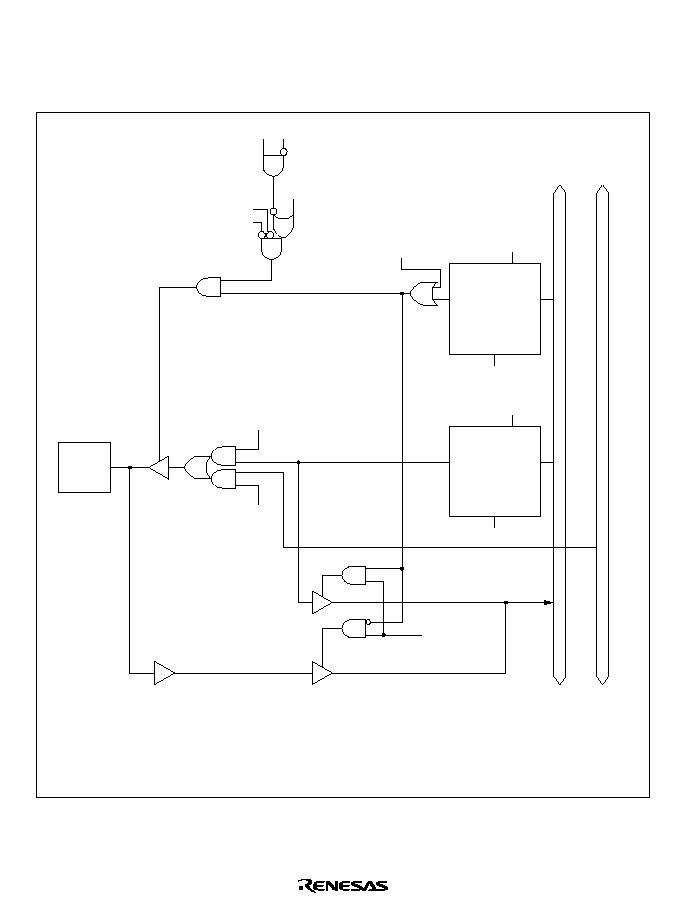
889
Appendix C I/O Port Block Diagrams
C.1
Port 1 Block Diagram
Reset
R
P1 DDR
n
Modes 1 to 4
WP1D
Q
D
C
Reset
R
P1 DR
n
WP1
Q
D
C
RP1
Mode 7
Modes
1 to 5
Internal data bus (upper)
Internal address bus
WP1D:
WP1:
RP1:
SSOE:
n = 0 to 7
Write to P1DDR
Write to port 1
Read port 1
Software standby output port enable
P1
n
External bus
released
Hardware standby
Software
standby
Mode 7
SSOE
Figure C.1 Port 1 Block Diagram
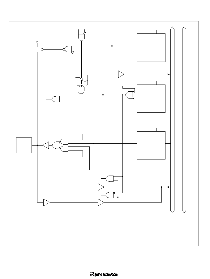
890
C.2
Port 2 Block Diagram
Reset
R
P2 DR
n
WP2
Q
D
C
Reset
R
P2 DDR
n
WP2D
Q
D
C
Reset
R
P2 PCR
n
WP2P
Q
D
C
Mode 7
Modes
1 to 5
Internal data bus (upper)
Internal address bus
P2
n
RP2P
RP2
WP2P:
RP2P:
WP2D:
WP2:
RP2:
SSOE:
n = 0 to 7
Write to P2PCR
Read P2PCR
Write to P2DDR
Write to port 2
Read port 2
Software standby output port enable
External bus
released
Hardware standby
Software
standby
Mode 7
Modes 1 to 4
SSOE
Figure C.2 Port 2 Block Diagram
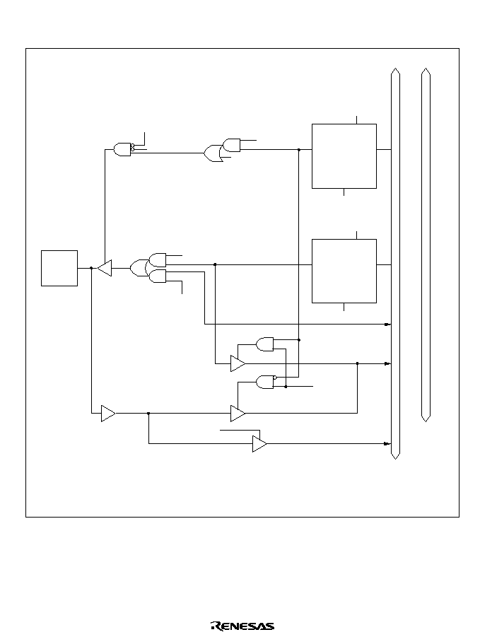
891
C.3
Port 3 Block Diagram
P3
n
Reset
R
P3 DDR
n
WP3D
Q
D
C
Reset
R
P3 DR
n
WP3
Q
D
C
RP3
Modes
1 to 5
Internal data bus (upper)
WP3D:
WP3:
RP3:
n = 0 to 7
Write to P3DDR
Write to port 3
Read port 3
Mode 7
Write to external
address
Mode 7
Hardware standby
External
bus released
Read external
address
Internal data bus (lower)
Figure C.3 Port 3 Block Diagram
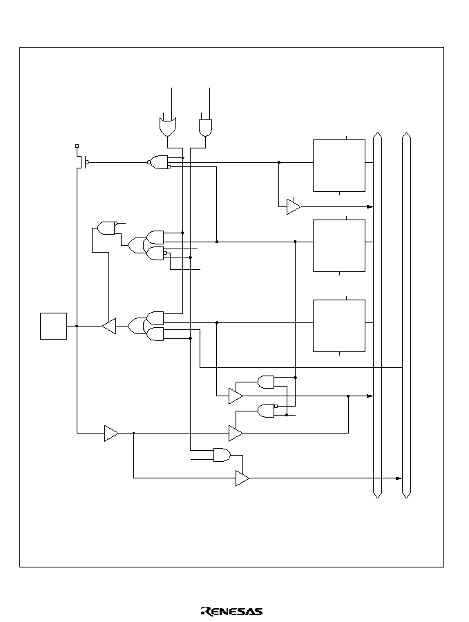
892
C.4
Port 4 Block Diagram
P4
n
RP4P
RP4
WP4
WP4D
WP4P
Reset
Reset
Reset
Q
D
R
C
P4 PCR
n
Q
D
R
C
P4 DDR
n
Q
D
R
C
P4 DR
n
WP4P:
RP4P:
WP4D:
WP4:
RP4:
n = 0 to 7
Write to P4PCR
Read P4PCR
Write to P4DDR
Write to port 4
Read port 4
Write to external
address
External bus
release
Hardware
standby
Read external
address
Internal data bus (upper)
Internal data bus (lower)
8-bit bus
mode
Mode 7
Modes
1 to 5
16-bit bus
mode
Figure C.4 Port 4 Block Diagram
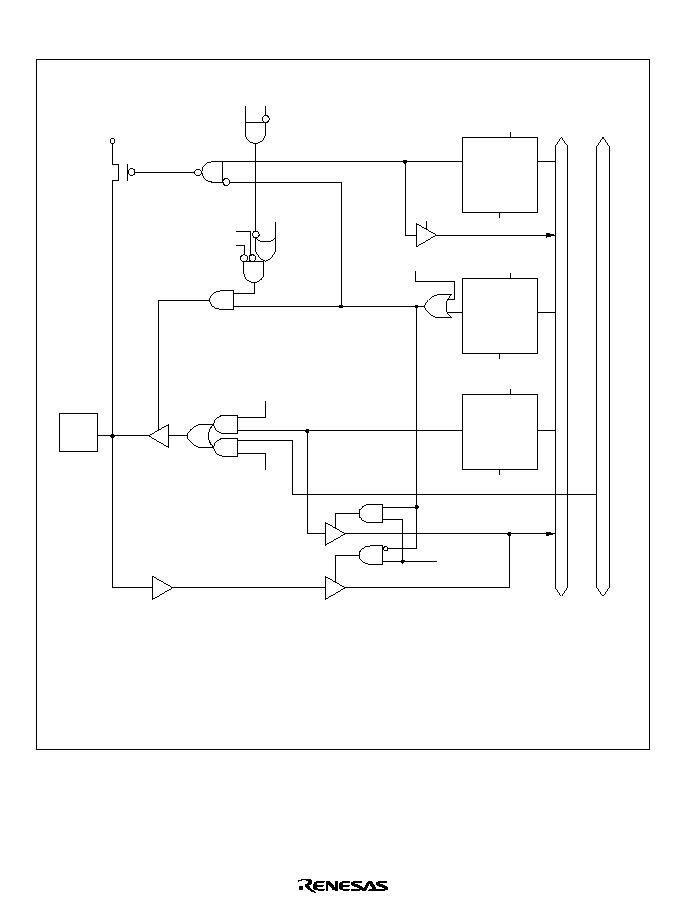
893
C.5
Port 5 Block Diagram
P5
n
RP5P
RP5
WP5
WP5D
WP5P
Reset
Reset
Reset
Q
D
R
C
P5 PCR
n
Q
D
R
C
P5 DDR
n
Q
D
R
C
P5 DR
n
WP5P:
RP5P:
WP5D:
WP5:
RP5:
SSOE:
n = 0 to 3
Write to P5PCR
Read P5PCR
Write to P5DDR
Write to port 5
Read port 5
Software standby output port enable
Mode 7
Modes
1 to 5
Internal data bus (upper)
Internal address bus
External bus
released
Hardware standby
Software
standby
Mode 7
Modes 1 to 4
SSOE
Figure C.5 Port 5 Block Diagram
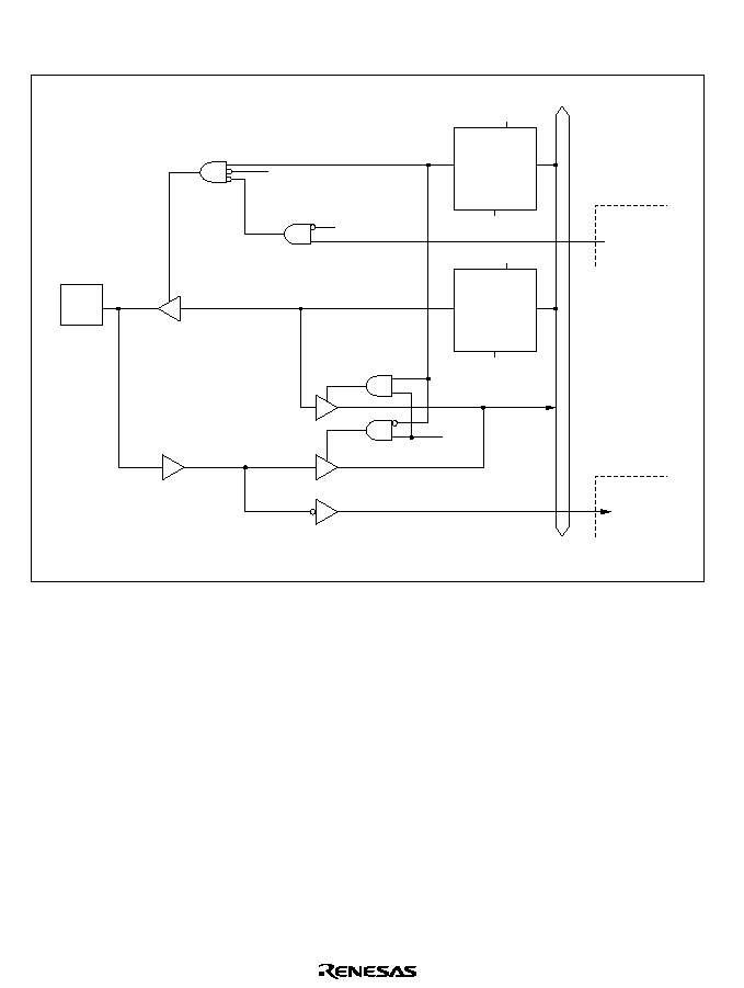
894
C.6
Port 6 Block Diagrams
WP6D:
WP6:
RP6:
Write to P6DDR
Write to port 6
Read port 6
RP6
input
WP6D
Reset
Q
D
R
C
P6 DDR
0
WP6
Reset
Q
D
R
C
P6 DR
0
P6
0
Internal data bus
Bus controller
WAIT
input
enable
Bus controller
WAIT
Mode 7
Hardware standby
Figure C.6 (a) Port 6 Block Diagram (Pin P6
0
)
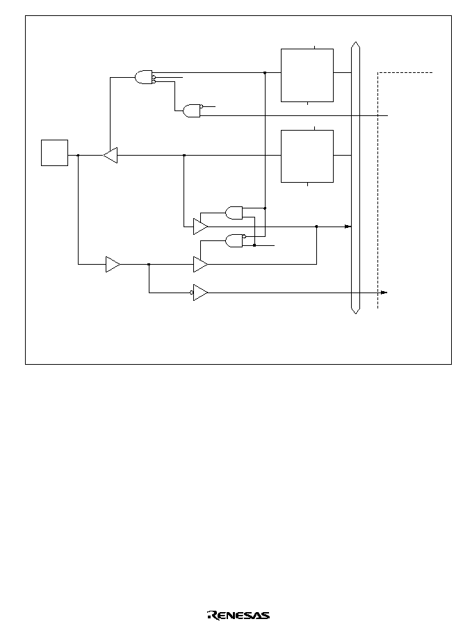
895
P6
1
WP6D:
WP6:
RP6:
Write to P6DDR
Write to port 6
Read port 6
WP6D
Reset
Q
D
R
C
P6 DDR
1
WP6
Reset
Q
D
R
C
P6 DR
1
RP6
Internal data bus
Bus
controller
Bus release
enable
BREQ input
Mode 7
Hardware standby
Figure C.6 (b) Port 6 Block Diagram (Pin P6
1
)
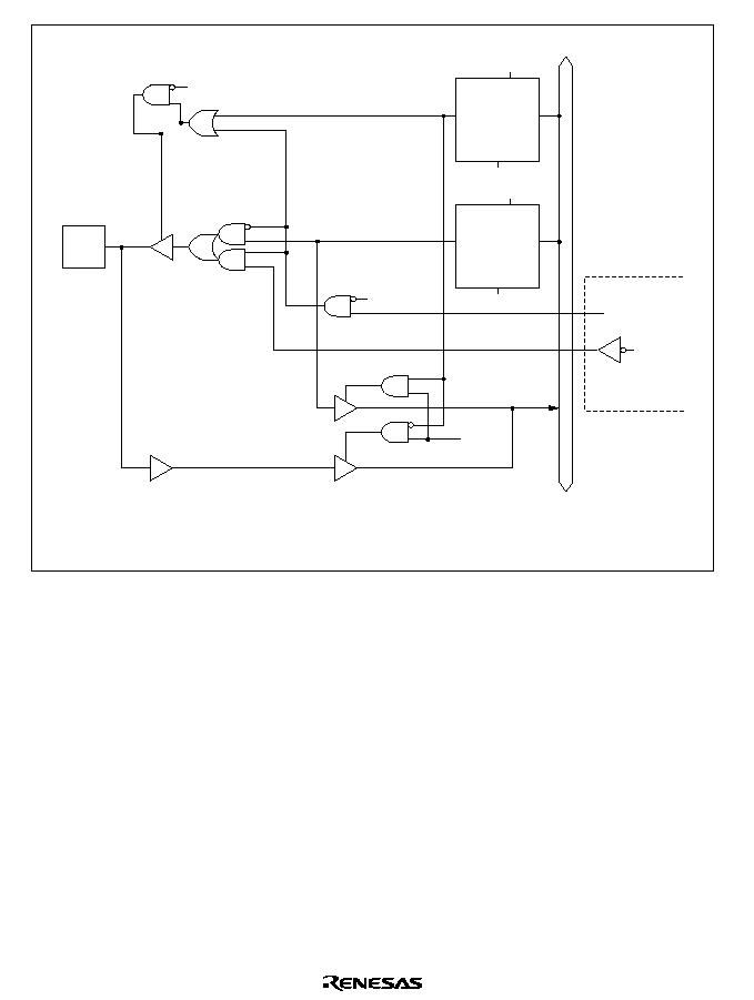
896
WP6D
Reset
Q
D
R
C
P6 DDR
2
WP6
Reset
Q
D
R
C
P6 DR
2
RP6
P6
2
WP6D:
WP6:
RP6:
Write to P6DDR
Write to port 6
Read port 6
Internal data bus
Bus controller
Bus release
enable
BACK
output
Mode 7
Hardware standby
Figure C.6 (c) Port 6 Block Diagram (Pin P6
2
)
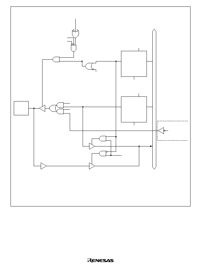
897
P6
3
Reset
R
P6 DDR
3
WP6D
Q
D
C
Reset
R
P6 DR
3
WP6
Q
D
C
RP6
Modes
1 to 5
Internal data bus
WP6D:
WP6:
RP6:
SSOE:
Write to P6DDR
Write to port 6
Read port 6
Software standby output port enable
Mode 7
Mode 7
AS output
Bus controller
External bus
released
Hardware standby
Software
standby
Mode 7
SSOE
Figure C.6 (d) Port 6 Block Diagram (Pin P6
3
)
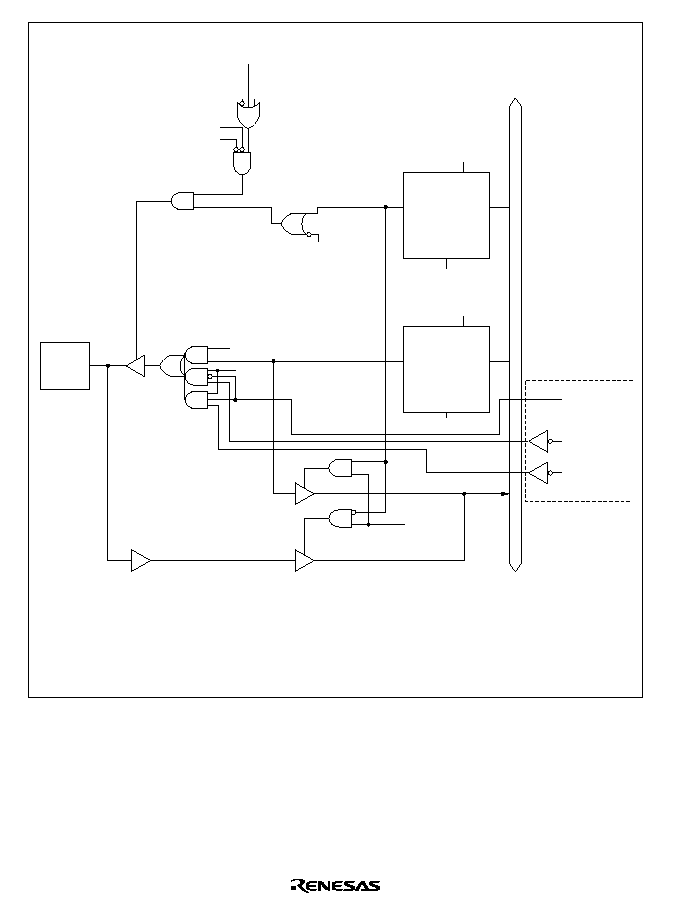
898
P6
4
Reset
R
P6 DDR
4
WP6D
Q
D
C
Reset
R
P6 DR
4
WP6
Q
D
C
RP6
Modes
1 to 5
Internal data bus
WP6D:
WP6:
RP6:
SSOE:
Write to P6DDR
Write to port 6
Read port 6
Software standby output port enable
Mode 7
Mode 7
RD output
WE output
enable
Bus controller
WE output
External bus
released
Hardware standby
Software
standby
Mode 7
SSOE
Figure C.6 (e) Port 6 Block Diagram (Pin P6
4
)
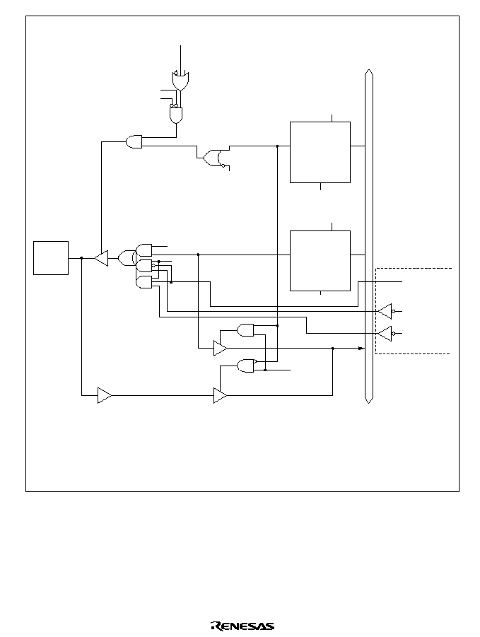
899
P6
n
Reset
R
P6 DDR
n
WP6D
Q
D
C
Reset
R
P6 DR
n
WP6
Q
D
C
RP6
Modes
1 to 5
Internal data bus
WP6D:
WP6:
RP6:
SSOE:
n = 5 and 6
Write to P6DDR
Write to port 6
Read port 6
Software standby output port enable
Mode 7
Mode 7
HWR output
LWR output
CAS output
enable
Bus controller
UCAS output
LCAS output
External bus
released
Hardware standby
Software
standby
Mode 7
SSOE
Figure C.6 (f) Port 6 Block Diagram (Pins P6
5
and P6
6
)
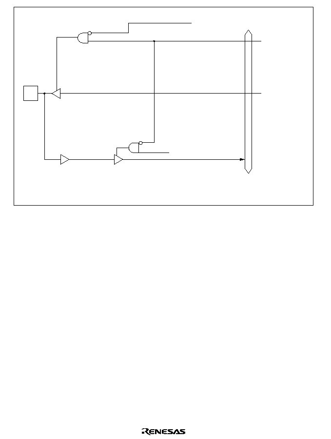
900
Read port 6
RP6:
Hardware standby
RP6
P6
7
output
output enable
Internal data bus
Figure C.6 (g) Port 6 Block Diagram (Pin P6
7
)
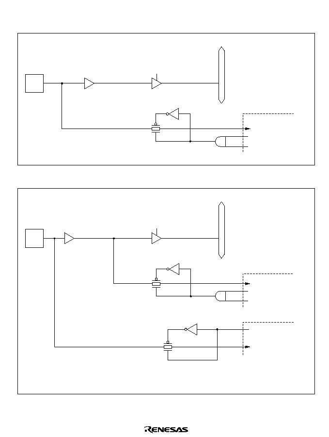
901
C.7
Port 7 Block Diagrams
P7
n
RP7
RP7: Read port 7
n = 0 to 5
Internal data bus
A/D converter
Input enable
Channel select signal
Analog input
Figure C.7 (a) Port 7 Block Diagram (Pins P7
0
to P7
5
)
P7
n
RP7
RP7: Read port 7
n = 6 and 7
Internal data bus
D/A converter
Analog output
Output enable
A/D converter
Input enable
Channel select signal
Analog input
Figure C.7 (b) Port 7 Block Diagram (Pins P7
6
and P7
7
)
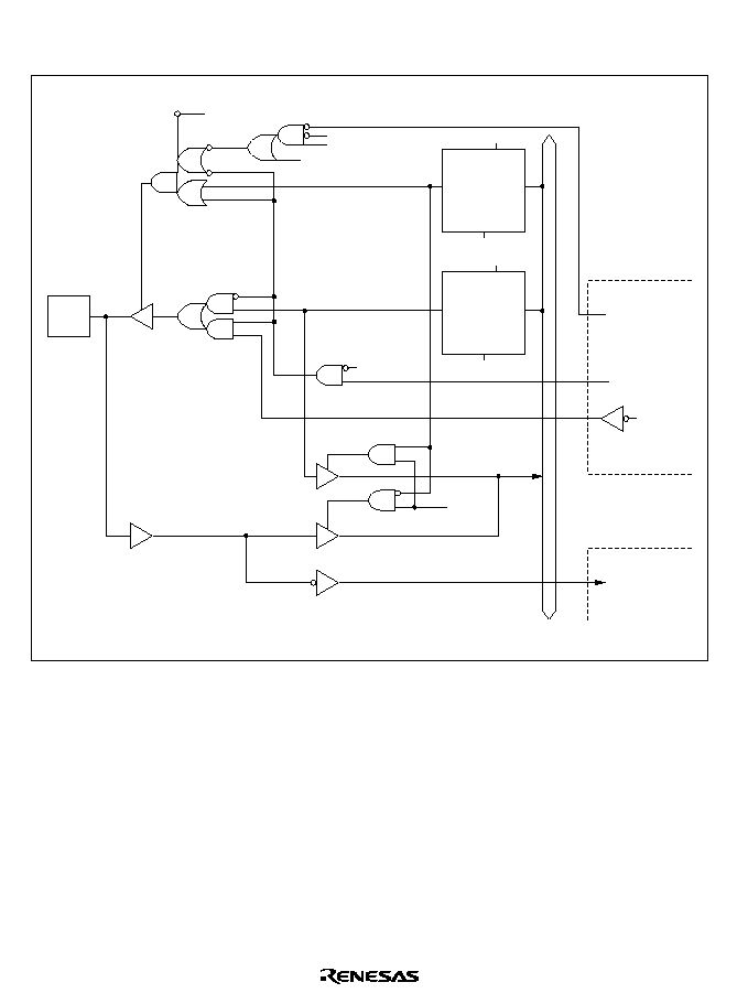
902
C.8
Port 8 Block Diagrams
P8
0
RP8
WP8D
Reset
External bus
released
Hardware
standby
SSOE
Software standby
Q
D
R
C
P8 DDR
0
WP8
Reset
Q
D
R
C
P8 DR
0
WP8D:
WP8:
RP8:
SSOE:
Write to P8DDR
Write to port 8
Read port 8
Software standby output port enable
Internal data bus
Bus controller
RFSH output
enable
Self-refresh
output enable
output
Interrupt
controller
input
RFSH
IRQ
0
Mode 7
Figure C.8 (a) Port 8 Block Diagram (Pin P8
0
)
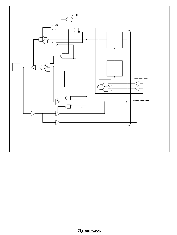
903
P8
n
WP8D
Reset
Q
D
R
C
P8 DDR
1
WP8
Reset
Q
D
R
C
P8 DR
1
RP8
WP8D:
WP8:
RP8:
SSOE:
Write to P8DDR
Write to port 8
Read port 8
Software standby output port enable
Internal data bus
Bus controller
Interrupt
controller
IRQ
1
input
CS
3
output
RAS
3
output
RAS
3
output enable
Area 3 DRAM
connection enable
Mode 7
Modes 1 to 5
SSOE
Hardware standby
Software standby
External bus release
Figure C.8 (b) Port 8 Block Diagram (Pin P8
1
)
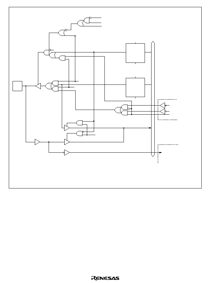
904
P8
2
WP8D
Reset
Q
D
R
C
P8 DDR
2
WP8
Reset
Q
D
R
C
P8 DR
2
RP8
WP8D:
WP8:
RP8:
SSOE:
Write to P8DDR
Write to port 8
Read port 8
Software standby output port enable
Internal data bus
Bus controller
Interrupt
controller
IRQ
2
input
CS
2
output
RAS
2
output
RAS
2
output enable
Mode 7
Modes 1 to 5
SSOE
Hardware
standby
Software standby
External bus release
Figure C.8 (c) Port 8 Block Diagram (Pin P8
2
)
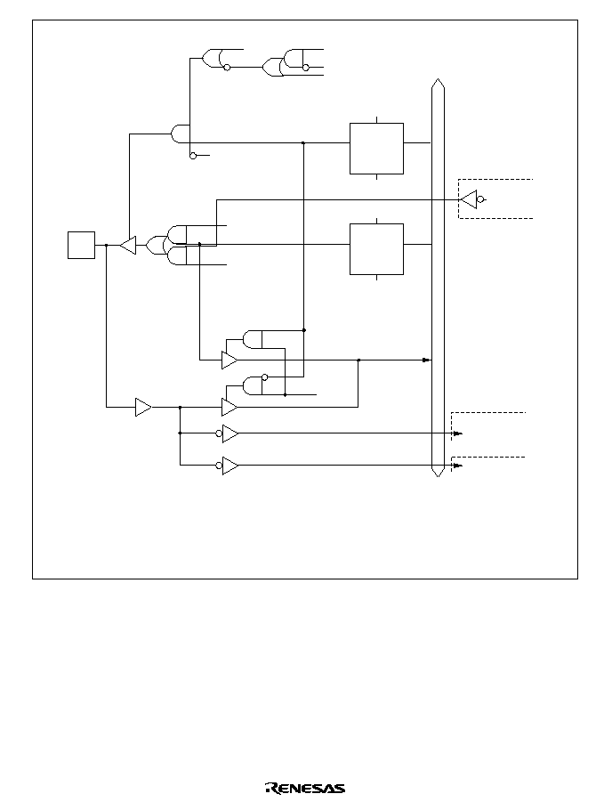
905
A/D converter
WP8D
P8
3
DR
C
Q
D
Write to P8DDR
Write to port 8
Read port 8
Software standby output port enable
WP8D:
WP8:
RP8:
SSOE:
WP8
R
Reset
Internal data bus
RP8
P8
3
Bus controller
CS
1
output
Reset
Mode 7
Modes 1 to 5
Interrupt controller
IRQ
3
input
ADTRG input
Mode 7
SSOE
External bus release
Software standby
Hardware standby
P8
3
DDR
C
Q
D
R
Figure C.8 (d) Port 8 Block Diagram (Pin P8
3
)
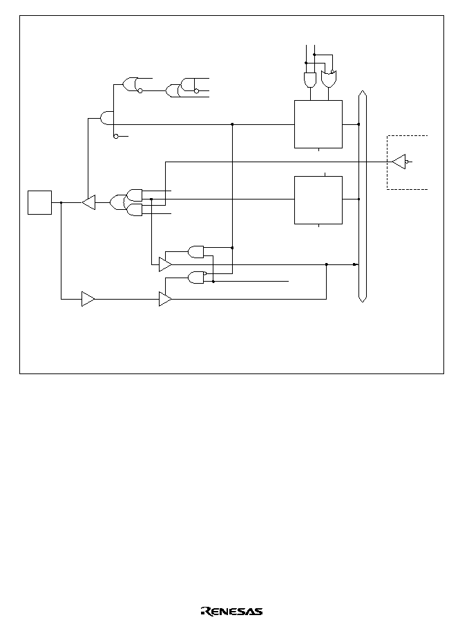
906
P8
4
WP8D
Q
D
S
C
P8 DDR
4
WP8
Reset
Reset
Modes 1 to 4
Q
D
R
C
P8 DR
4
RP8
WP8D:
WP8:
RP8:
SSOE:
Write to P8DDR
Write to port 8
Read port 8
Software standby output port enable
Internal data bus
Bus controller
output
0
CS
Mode 7
Modes 1 to 5
R
Mode 7
SSOE
External bus release
Software standby
Hardware standby
Figure C.8 (e) Port 8 Block Diagram (Pin P8
4
)
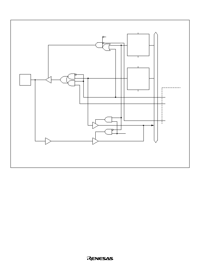
907
C.9
Port 9 Block Diagrams
WP9D:
WP9:
RP9:
Write to P9DDR
Write to port 9
Read port 9
P9
0
RP9
WP9D
Reset
Hardware
standby
Q
D
R
C
P9 DDR
0
WP9
Reset
Q
D
R
C
P9 DR
0
Internal data bus
SCI
Output
enable
Serial
transmit
data
Guard
time
Figure C.9 (a) Port 9 Block Diagram (Pin P9
0
)
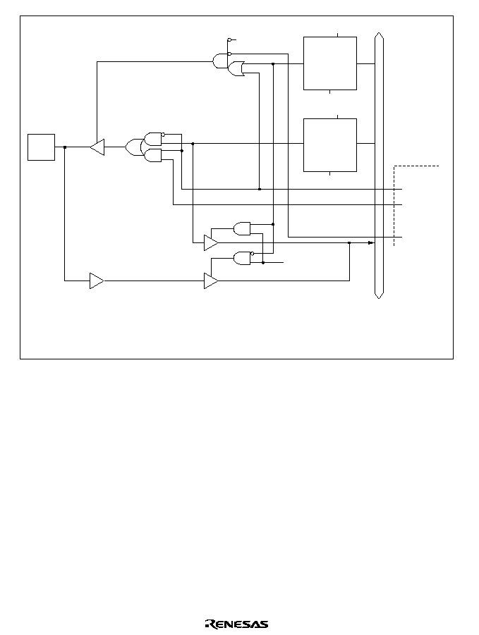
908
WP9D:
WP9:
RP9:
Write to P9DDR
Write to port 9
Read port 9
P9
1
RP9
WP9D
Reset
Q
D
R
C
P9 DDR
1
WP9
Reset
Q
D
R
C
P9 DR
1
Internal data bus
SCI
Output
enable
Serial
transmit
data
Guard time
Hardware
standby
Figure C.9 (b) Port 9 Block Diagram (Pin P9
1
)
909
WP9D:
WP9:
RP9:
Write to P9DDR
Write to port 9
Read port 9
P9
2
WP9D
Reset
Q
D
R
C
P9 DDR
2
WP9
Reset
Q
D
R
C
P9 DR
2
RP9
Internal data bus
Input enable
Serial receive
data
SCI
Hardware standby
Figure C.9 (c) Port 9 Block Diagram (Pin P9
2
)
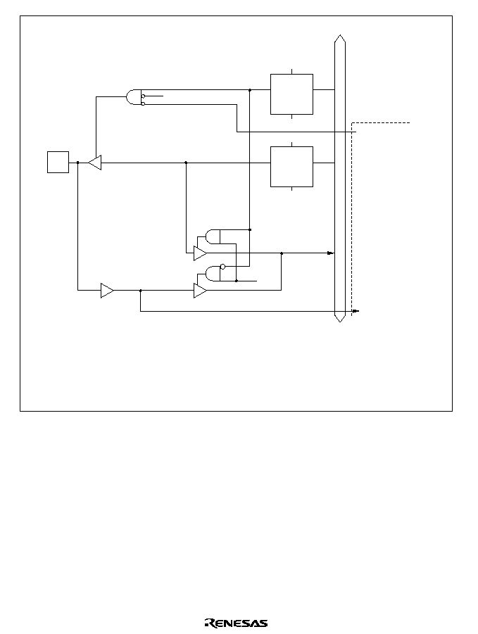
910
P9
3
DDR
C
Q
D
WP9D
RP9
P9
3
DR
C
Q
D
P9
3
Serial receive data
Input enable
Write to P9DDR
Write to port 9
Read port 9
WP9D:
WP9:
RP9:
WP9
R
R
Reset
Internal data bus
Reset
SCI
Hardware standby
Figure C.9 (d) Port 9 Block Diagram (Pin P9
3
)
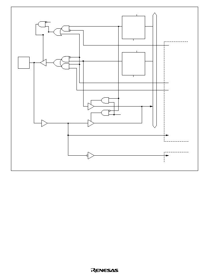
911
WP9D:
WP9:
RP9:
Write to P9DDR
Write to port 9
Read port 9
WP9D
Reset
Q
D
R
C
P9 DDR
4
WP9
Reset
Q
D
R
C
P9 DR
4
RP9
P9
4
Internal data bus
SCI
Clock input
enable
Clock output
enable
Clock output
Clock input
Interrupt
controller
input
IRQ
4
Hardware standby
Figure C.9 (e) Port 9 Block Diagram (Pin P9
4
)
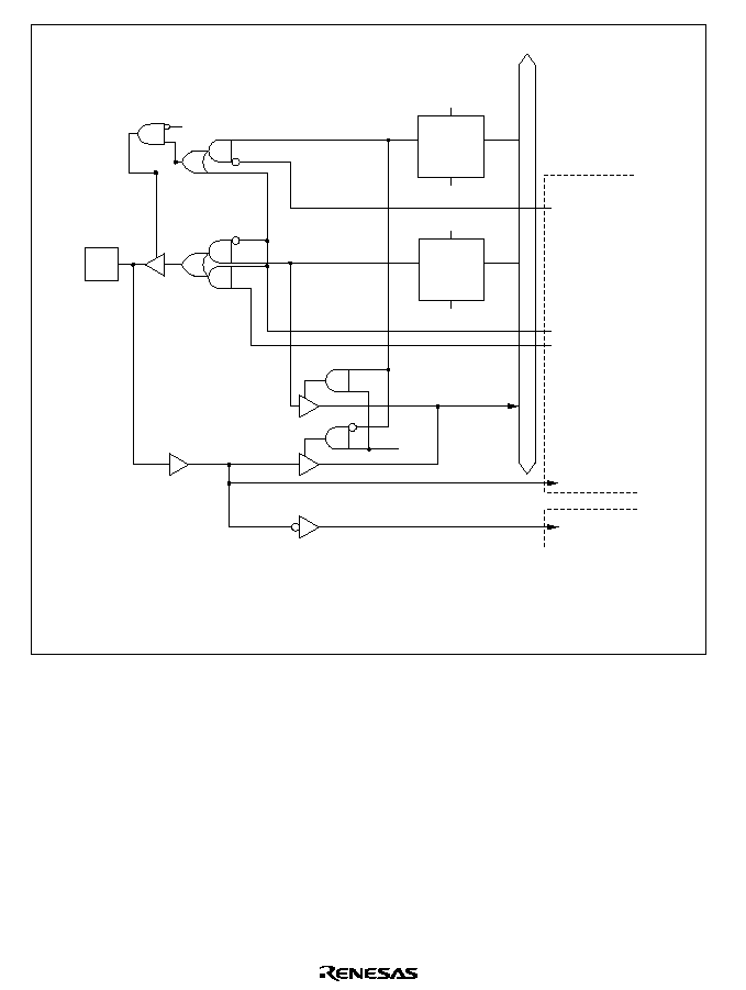
912
R
P9
5
DDR
C
Q
D
Reset
WP9D
WP9
RP9
R
P9
5
DR
C
Q
D
Reset
P9
5
SCI
Clock input
enable
Clock output
enable
Clock output
Interrupt controller
IRQ
5
input
Clock input
Write to P9DDR
Write to port 9
Read port 9
WP9D:
WP9:
RP9:
Internal data bus
Hardware standby
Figure C.9 (f) Port 9 Block Diagram (Pin P9
5
)
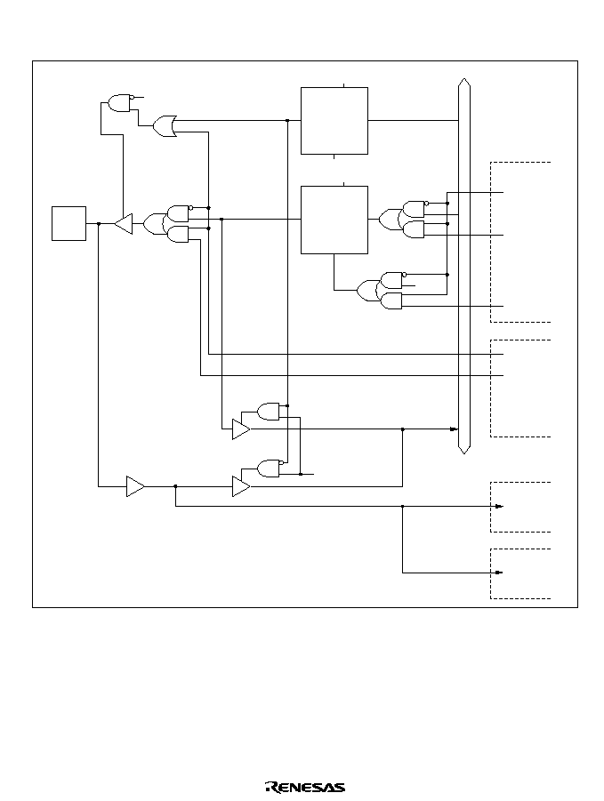
913
C.10
Port A Block Diagrams
WPAD:
WPA:
RPA:
n = 0 and 1
Write to PADDR
Write to port A
Read port A
PA
n
WPAD
Reset
Q
D
R
C
PA DDR
n
Reset
Q
D
R
C
PA DR
n
RPA
WPA
Internal data bus
TPC
output
enable
TPC
Next data
Output
trigger
Output
enable
Transfer
end output
DMA controller
Counter
clock input
16-bit timer
Counter
clock input
8-bit timer
Hardware standby
Figure C.10 (a) Port A Block Diagram (Pins PA
0
, PA
1
)
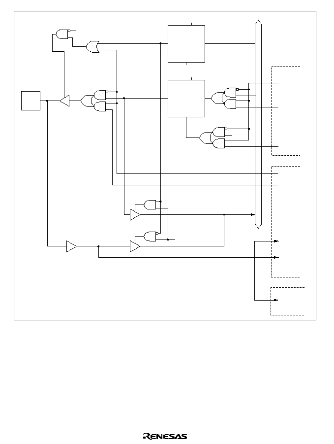
914
WPAD:
WPA:
RPA:
n = 2 and 3
Write to PADDR
Write to port A
Read port A
PA
n
RPA
WPA
WPAD
Reset
Q
D
R
C
PA DDR
n
Reset
Q
D
R
C
PA DR
n
Internal data bus
TPC
output
enable
TPC
Next
data
Output
trigger
Output
enable
Compare
match
output
Input
capture
Counter
clock
input
16-bit timer
Counter
clock input
8-bit timer
Hardware standby
Figure C.10 (b) Port A Block Diagram (Pins PA
2
, PA
3
)
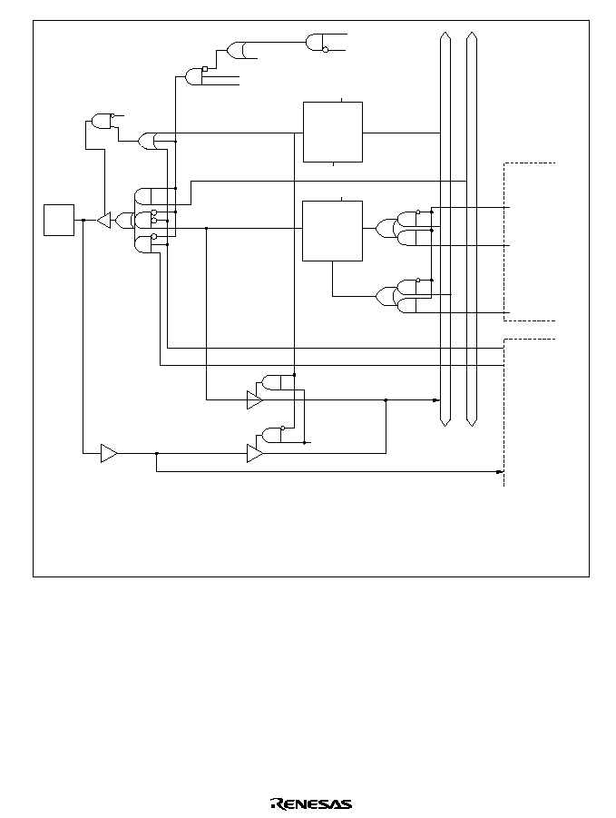
915
WPAD:
WPA:
RPA:
SSOE:
n = 4 to 7
Note: The PA
7
address output enable setting is fixed at 1 in modes 3 and 4.
Write to PADDR
Write to port A
Read port A
Software standby output port enable
PA
n
WPAD
Reset
PRA
WPA
Q
D
R
C
PA
n
DDR
Reset
Q
D
R
C
PA
n
DR
Internal address bus
Internal data bus
TPC
16-bit timer
TPC output
enable
Next data
Output trigger
Output enable
Compare match
output
Input capture
Software standby
SSOE
Bus released
Mode 3/4
Address output enable
Hardware
standby
Figure C.10 (c) Port A Block Diagram (Pins PA
4
to PA
7
)
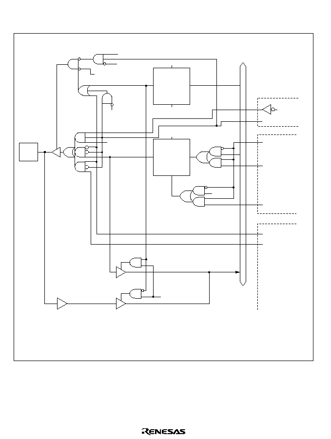
916
C.11
Port B Block Diagrams
PB
0
WPBD:
WPB:
RPB:
SSOE:
Write to PBDDR
Write to port B
Read port B
Software standby output port enable
Reset
Q
D
R
C
PB DDR
0
WPBD
Reset
Q
D
R
C
PB DR
0
WPB
RPB
Internal data bus
TPC output
enable
TPC
Next data
Output trigger
Output enable
Compare
match output
8-bit timer
Modes
1 to 5
Bus released
Bus controller
CS output enable
CS7
output
Software
standby
SSOE
Hardware standby
Figure C.11 (a) Port B Block Diagram (Pin PB
0
)
917
R
PB
1
DDR
C
Q
D
Reset
Modes
1 to 5
WPBD
WPB
RPB
R
PB
1
DR
C
Q
D
Reset
PB
1
TPC
8-bit timer
TPC output enable
Bus controller
CS output enable
CS6 output
Next data
Output trigger
Output enable
Compare match output
DMAC
DREQ0
DREQ1 input
TMO2
TMO3 input
Write to PBDDR
Write to port B
Read port B
Software standby output port enable
WPBD:
WPB:
RPB:
SSOE:
Bus released
Software standby
SSOE
Internal data bus
Hardware
standby
Figure C.11 (b) Port B Block Diagram (Pin PB
1
)
918
R
PB
2
DDR
C
Q
D
Reset
WPBD
WPB
RPB
R
PB
2
DR
C
Q
D
Reset
PB
2
TPC
8-bit timer
TPC output enable
Bus controller
RAS
5
output enable
RAS
5
output
CS
5
output
CS
5
output enable
Area 5 DRAM connection
output enable
Next data
Output trigger
Output enable
Compare match output
Write to PBDDR
Write to port B
Read port B
Software standby output port enable
WPBD:
WPB:
RPB:
SSOE:
Note: Area 5 DRAM connection output enable, RAS
5
output enable,
and CS
5
output enable are all fixed at 0 in mode 7.
Internal data bus
Software standby
External bus release
SSOE
Hardware
standby
Mode 7
Figure C.11 (c) Port B Block Diagram (Pin PB
2
)
919
R
PB
3
DDR
C
Q
D
Reset
WPBD
WPB
RPB
R
PB
3
DR
C
Q
D
Reset
PB
3
TPC
8-bit timer
TMIO
3
input
DREQ
1
input
DMAC
TPC output enable
Bus controller
RAS
4
output enable
RAS
4
output
CS
4
output
CS
4
output enable
Area 4 DRAM connection
output enable
Next data
Output trigger
Output enable
Compare match output
Write to PBDDR
Write to port B
Read port B
Software standby output port enable
WPBD:
WPB:
RPB:
SSOE:
Internal data bus
Software standby
External bus release
SSOE
Hardware
standby
Mode 7
Note: Area 4 DRAM connection output enable, RAS
4
output enable,
and CS
4
output enable are all fixed at 0 in mode 7.
Figure C.11 (d) Port B Block Diagram (Pin PB
3
)
920
PB
4
WPBD:
WPB:
RPB:
SSOE:
Write to PBDDR
Write to port B
Read port B
Software standby output port enable
Note: In mode 7, CAS output enable is fixed at 0.
WPB
RPB
Reset
Hardware standby
External bus release
SSOE
Software standby
Q
D
R
C
PB DDR
4
WPBD
Reset
Q
D
R
C
PB DR
4
Internal data bus
TPC output
enable
Next data
Output trigger
Output enable
CAS output
TPC
Bus controller
Figure C.11 (e) Port B Block Diagram (Pin PB
4
)
921
R
PB
5
DDR
C
Q
D
Reset
WPBD
WPB
RPB
R
PB
5
DR
C
Q
D
Reset
PB
5
TPC
SCI
TPC output enable
SCI
Next data
Output trigger
Clock output
enable
Clock input
enable
Clock output
Clock input
Write to PBDDR
Write to port B
Read port B
Software standby output port enable
Bus controller
CAS output enable
CAS output
WPBD:
WPB:
RPB:
SSOE:
Internal data bus
Hardware
standby
External bus release
SSOE
Software standby
Note: In mode 7, CAS output enable is fixed at 0.
Figure C.11 (f) Port B Block Diagram (Pin PB
5
)
922
WPBD
Reset
Hardware standby
Reset
Q
D
R
C
PB DDR
Q
D
R
C
PB DR
6
RPB
WPB
TPC
SCI
WPBD:
WPB:
RPB:
Write to PBDDR
Write to port B
Read port B
TPC
output
enable
Next data
Output
trigger
Output enable
Serial transmit data
Guard time
Internal data bus
6
PB
6
Figure C.11 (g) Port B Block Diagram (Pin PB
6
)
923
PB
7
WPBD
Reset
Reset
Q
D
R
C
PB DDR
Q
D
R
C
PB DR
7
RPB
WPB
SCI
TPC
SCI
WPBD:
WPB:
RPB:
Write to PBDDR
Write to port B
Read port B
TPC
output
enable
Input enable
Next data
Output
trigger
Inter
nal data b
u
s
7
Serial receive
data
Hardware standby
Figure C.11 (h) Port B Block Diagram (Pin PB
7
)

924
Appendix D Pin States
D.1
Port States in Each Mode
Table D.1
Port States
Pin
Name
Mode
Reset
Hardware
Standby
Mode
Software Standby
Mode
Bus-Released
Mode
Program Execution
Mode
P1
7
to
P1
0
1 to 4
L
T
(SSOE=0)
T
(SSOE=1)
Keep
T
A
7
to A
0
5
T
T
(DDR = 0)
Keep
(DDR=1, SSOE=0)
T
(DDR=1, SSOE=1)
Keep
T
(DDR=0)
Input port
(DDR=1)
A
7
to A
0
7
T
T
Keep
--
I/O port
P2
7
to
P2
0
1 to 4
L
T
(SSOE = 0)
T
(SSOE = 1)
Keep
T
A
15
to A
8
5
T
T
(DDR = 0)
Keep
(DDR=1,SSOE=0)
T
(DDR=1,SSOE=1)
Keep
T
(DDR=0)
Input port
(DDR=1)
A
15
to A
8
7
T
T
Keep
--
I/O port
P3
7
to
P3
0
1 to 5
T
T
T
T
D
15
to D
8
7
T
T
Keep
--
I/O port
P4
7
to
P4
0
1, 3, 5 T
T
Keep
Keep
I/O port
2, 4
T
T
T
T
D
7
to D
0
7
T
T
Keep
--
I/O port

925
Pin
Name
Mode
Reset
Hardware
Standby
Mode
Software Standby
Mode
Bus-Released
Mode
Program Execution
Mode
P5
3
to
P5
0
1 to 4
L
T
(SSOE=0)
T
(SSOE=1)
Keep
T
A
19
to A
16
5
T
T
(DDR=0)
Keep
(DDR=1, SSOE=0)
T
(DDR=1, SSOE=1)
Keep
T
(DDR=0)
Input port
(DDR=1)
A
19
to A
16
7
T
T
Keep
--
I/O port
P6
0
1 to 5
T
T
Keep
Keep
I/O port
WAIT
7
T
T
Keep
--
I/O port
P6
1
1 to 5
T
T
(BRLE=0)
Keep
(BRLE=1)
T
T
I/O port
BREQ
7
T
T
Keep
--
I/O port
P6
2
1 to 5
T
T
(BRLE=0)
Keep
(BRLE=1)
H
L
(BRLE=0)
I/O port
(BRLE=1)
BACK
7
T
T
Keep
--
I/O port
P6
6
to
P6
3
1 to 5
H
T
(SSOE=0)
T
(SSOE=1)
H
T
AS
,
RD
,
HWR
,
LWR
7
T
T
Keep
--
I/O port
P6
7
1 to 5
Clock
output
T
(PSTOP=0)
H
(PSTOP=1)
Keep
(PSTOP=0)
(PSTOP=1)
Keep
(PSTOP=0)
(PSTOP=1)
Input port
7
T
T
(PSTOP=0)
H
(PSTOP=1)
Keep
(PSTOP=0)
(PSTOP=1)
Keep
(PSTOP=0)
(PSTOP=1)
Input port
P7
7
to
P7
0
1 to
5, 7
T
T
T
T
Input port

926
Pin
Name
Mode
Reset
Hardware
Standby
Mode
Software Standby
Mode
Bus-Released
Mode
Program Execution
Mode
P8
0
1 to 5
T
T
When DRAM space is
not selected
*
1
(RFSHE=0)
Keep
(RFSHE=1)
Illegal setting
When DRAM space is
selected
*
2
(RFSHE=0)
Keep
(RFSHE=1, SRFMD=0,
SSOE=0)
T
(RFSHE=1, SRFMD=0,
SSOE=1)
H
(RFSHE=1, SRFMD=1)
RFSH
When DRAM space is
selected
*
1
(RFSHE=0)
Keep
(RFSHE=1)
Illegal setting
When DRAM space is
selected
*
2
(RFSHE=0)
Keep
(RFSHE=1)
T
(RFSHE=0)
I/O port
(RFSHE=1)
RFSH
7
T
T
Keep
--
I/O port
P8
1
1 to 5
T
T
When DRAM space is
selected and RAS
3
is
output
*
3
(SSOE=0)
T
(SSOE=1)
H
When DRAM space is
selected and RAS
3
is
not output
*
4
Keep
Otherwise
*
5
*
1
(DDR=0)
T
(DDR=1, SSOE=0)
T
(DDR=1, SSOE=1)
H
When DRAM space is
selected and RAS
3
is
output
*
3
T
When DRAM space is
selected and RAS
3
is
not output
*
4
Keep
Otherwise
*
1
(DDR=0)
Keep
(DDR=1)
T
When DRAM space is
selected and RAS
3
is
output
RAS
3
When DRAM space is
selected and RAS
3
is
not output
I/O port
Otherwise
(DDR=0)
Input port
(DDR=1)
CS
3
7
T
T
Keep
--
I/O port

927
Pin
Name
Mode
Reset
Hardware
Standby
Mode
Software Standby
Mode
Bus-Released
Mode
Program Execution
Mode
P8
2
1 to 5
T
T
RAS
2
output
*
2
(SSOE=0)
T
(SSOE=1)
H
Otherwise
*
1
(DDR=0)
T
(DDR=1, SSOE=0)
T
(DDR=1, SSOE=1)
H
RAS
2
output
*
2
T
Otherwise
*
1
(DDR=0)
Keep
(DDR=1)
T
RAS
2
output
RAS
2
Otherwise
(DDR=0)
I/O port
(DDR=1)
CS
2
7
T
T
Keep
--
I/O port
P8
3
1 to 5
T
T
(DDR=0)
T
(DDR=1, SSOE=0)
T
(DDR=1, SSOE=1)
H
(DDR=0)
Keep
(DDR=1)
T
(DDR=0)
Input port
(DDR=1)
CS
1
7
T
T
Keep
--
I/O port
P8
4
1 to 4
H
T
(DDR=0)
T
(DDR=1, SSOE=0)
T
(DDR=1, SSOE=1)
H
(DDR = 0)
Keep
(DDR = 1)
T
(DDR = 0)
Input port
(DDR = 1)
CS
0
5
T
T
(DDR=0)
T
(DDR=1, SSOE=0)
T
(DDR=1, SSOE=1)
H
(DDR=0)
Keep
(DDR=1)
T
(DDR=0)
Input port
(DDR=1)
CS
0
7
T
T
Keep
--
I/O port
P9
5
to
P9
0
1 to
5, 7
T
T
Keep
Keep
I/O port
PA
3
to
PA
0
1 to
5, 7
T
T
Keep
Keep
I/O port
PA
6
to
PA
4
1, 2, 7 T
T
Keep
Keep
I/O port

928
Pin
Name
Mode
Reset
Hardware
Standby
Mode
Software Standby
Mode
Bus-Released
Mode
Program Execution
Mode
PA
6
to
PA
4
3 to 5
T
T
Address output
*
5
(SSOE=0)
T
(SSOE=1)
Keep
Otherwise
*
6
Keep
Address output
*
5
T
Otherwise
*
6
Keep
Address output
A
23
to A
21
Otherwise
I/O port
PA
7
1, 2
T
T
Keep
Keep
I/O port
3, 4
L
T
(SSOE=0)
T
(SSOE=1)
Keep
T
A
20
5
L
T
When A20E = 0
SSOE = 0
T
SSOE = 1
Keep
When A20E = 1
Keep
When A20E = 0
T
When A20E = 1
Keep
When A20E = 0
A
20
When A20E = 1
I/O port
7
T
T
Keep
--
I/O port
PB
1
,
PB
0
1 to 5
T
T
CS output
*
7
(SSOE=0)
T
(SSOE=1)
H
Otherwise
*
8
Keep
CS output
*
7
T
Otherwise
*
8
Keep
CS output
CS
7
,
CS
6
Otherwise
I/O port
7
T
T
Keep
--
I/O port
PB
2
1 to 5
T
T
RAS
5
output
*
9
(SSOE=0)
T
(SSOE=1)
H
CS output
*
10
(SSOE=0)
T
(SSOE=1)
H
Otherwise
*
11
Keep
RAS
5
output
*
9
T
CS output
*
10
T
Otherwise
*
11
Keep
RAS
5
output
RAS
5
CS output
CS
5
Otherwise
I/O port
7
T
T
Keep
--
I/O port

929
Pin
Name
Mode
Reset
Hardware
Standby
Mode
Software Standby
Mode
Bus-Released
Mode
Program Execution
Mode
PB
3
1 to 5
T
T
RAS
4
output
*
12
(SSOE=0)
T
(SSOE=1)
H
CS output
*
13
(SSOE=0)
T
(SSOE=1)
H
Otherwise
*
14
Keep
RAS
4
output
*
12
T
CS output
*
13
T
Otherwise
*
14
Keep
RAS
4
output
RAS
4
CS output
CS
4
Otherwise
I/O port
7
T
T
Keep
--
I/O port
PB
5
,
PB
4
1 to 5
T
T
CAS output
*
15
(SSOE=0)
T
(SSOE=1)
H
Otherwise
*
16
Keep
CAS output
*
15
T
Otherwise
*
16
Keep
CAS output
UCAS
,
LCAS
Otherwise
I/O port
7
T
T
Keep
--
I/O port
PB
7
,
PB
6
1 to
5, 7
T
T
Keep
Keep
I/O port
Legend
H:
High
L:
Low
T:
High-impedance state
Keep: Input pins are in the high-impedance state; output pins maintain their previous state.
DDR: Data direction register
Notes:
*
1 When bits DRAS2, DRAS1, and DRAS0 in DRCRA (DRAM control register A) are all
cleared to 0.
*
2 When any of bits DRAS2, DRAS1, or DRAS0 in DRCRA (DRAM control register A) is
set to 1.
*
3 When the setting of bits DRAS2, DRAS1, and DRAS0 in DRCRA (DRAM control
register A) is 010, 100, or 101.
*
4 When the setting of bits DRAS2, DRAS1, and DRAS0 in DRCRA (DRAM control
register A) is other than 010, 100, 101, or 000.
*
5 When bit A23E, A22E, or A21E, respectively, in BRCR (bus release control register) is
cleared to 0.
*
6 When bit A23E, A22E, or A21E, respectively, in BRCR (bus release control register) is
set to 1.
*
7 When bit CS7E or CS6E, respectively, in CSCR (chip select control register) is set to
1.
*
8 When bit CS7E or CS6E, respectively, in CSCR (chip select control register) is cleared
to 0.

930
*
9 When the setting of bits DRAS2, DRAS1, and DRAS0 in DRCRA (DRAM control
register A) is 101.
*
10 When the setting of bits DRAS2, DRAS1, and DRAS0 in DRCRA (DRAM control
register A) is other than 101, and bit CS5E in CSCR (chip select control register) is set
to 1.
*
11 When the setting of bits DRAS2, DRAS1, and DRAS0 in DRCRA (DRAM control
register A) is other than 101, and bit CS5E in CSCR (chip select control register) is
cleared to 0.
*
12 When the setting of bits DRAS2, DRAS1, and DRAS0 in DRCRA (DRAM control
register A) is 100, 101, or 110.
*
13 When the setting of bits DRAS2, DRAS1, and DRAS0 in DRCRA (DRAM control
register A) is other than 100, 101, or 110, and bit CS4E in CSCR (chip select control
register) is set to 1.
*
14 When the setting of bits DRAS2, DRAS1, and DRAS0 in DRCRA (DRAM control
register A) is other than 100, 101, or 110, and bit CS4E in CSCR (chip select control
register) is cleared to 0.
*
15 When any of bits DRAS2, DRAS1, or DRAS0 in DRCRA (DRAM control register A) is
set to 1, and bit CSEL in DRCRB (DRAM control register B) is cleared to 0.
*
16 When any of bits DRAS2, DRAS1, or DRAS0 in DRCRA (DRAM control register A) is
set to 1, and bit CSEL in DRCRB (DRAM control register B) is set to 1; or, when bits
DRAS2, DRAS1, and DRAS0 are all cleared to 0.
931
D.2
Pin States at Reset
Modes 1 and 2: Figure D.1 is a timing diagram for the case in which
RES goes low during an
external memory access in mode 1 or 2. As soon as
RES goes low, all ports are initialized to the
input state.
AS, RD, HWR, LWR, and CS
0
go high, and D
15
to D
0
go to the high-impedance state.
The address bus is initialized to the low output level 2.5
clock cycles after the low level of
RES
is sampled. Clock pin P6
7
/
goes to the output state at the next rise of
after
RES goes low.
AS
,
RD
(read)
D
15
to D
0
(write)
HWR
,
LWR
(write)
Internal reset
signal
RES
P6
7
/
I/O port,
CS
7
to
CS
1
CS
0
A
19
to A
0
T1
T2
T3
Access to external
memory
H'00000
High impedance
High impedance
Figure D.1 Reset during Memory Access (Modes 1 and 2)
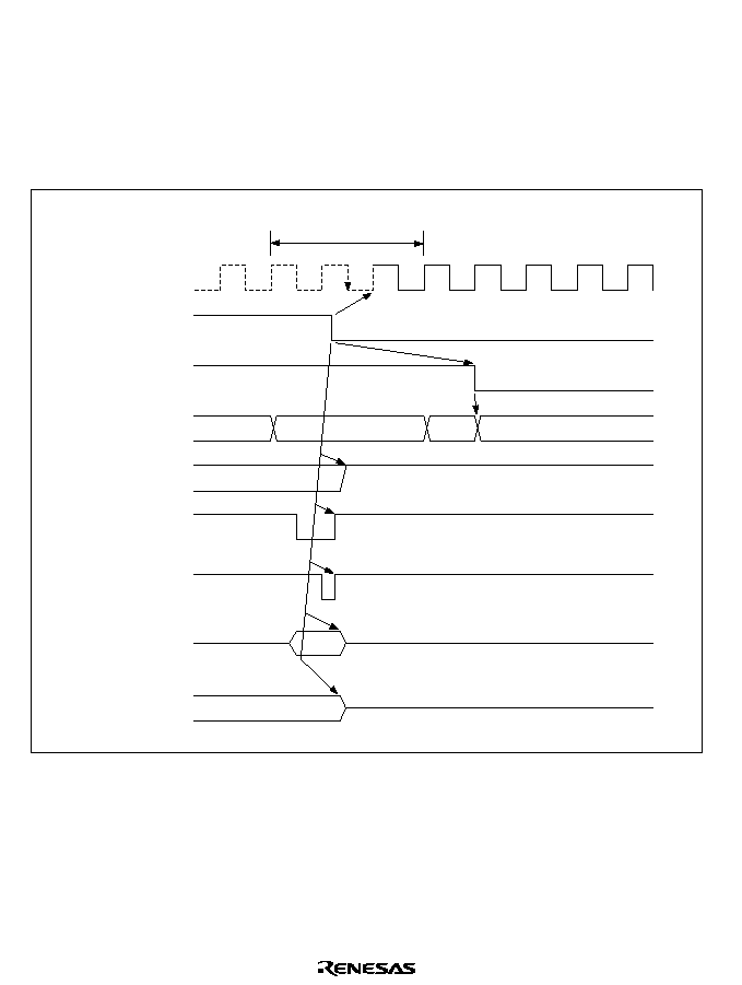
932
Modes 3 and 4: Figure D.2 is a timing diagram for the case in which
RES goes low during an
external memory access in mode 3 or 4. As soon as
RES goes low, all ports are initialized to the
input state.
AS, RD, HWR, LWR, and CS
0
go high, and D
15
to D
0
go to the high-impedance state.
The address bus is initialized to the low output level 2.5
clock cycles after the low level of
RES
is sampled. However, when PA
4
to PA
6
are used as address bus pins, or when P8
3
to P8
1
and PB
0
to PB
3
are used as CS output pins, they go to the high-impedance state at the same time as
RES
goes low. Clock pin P6
7
/
goes to the output state at the next rise of
after
RES goes low.
T1
T2
T3
Access to external
memory
H'000000
High impedance
High impedance
AS
,
RD
(read)
D
15
to D
0
(write)
HWR
,
LWR
(write)
Internal reset
signal
RES
P6
7
/
I/O port,
PA
4
/A
23
to PA
6
/A
21
,
CS
7
to
CS
1
CS
0
A
20
to A
0
Figure D.2 Reset during Memory Access (Modes 3 and 4)
Mode 5: Figure D.3 is a timing diagram for the case in which
RES goes low during an external
memory access in mode 5. As soon as
RES goes low, all ports are initialized to the input state. AS,
RD, HWR, and LWR go high, and the address bus and D
15
to D
0
go to the high-impedance state.
Clock pin P6
7
/
goes to the output state at the next rise of
after
RES goes low.
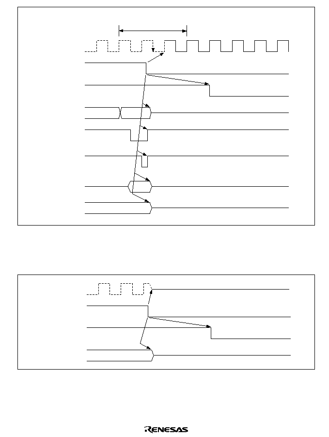
933
T1
T2
T3
Access to external
memory
High impedance
High impedance
High impedance
AS
,
RD
(read)
D
15
to D
0
(write)
HWR
,
LWR
(write)
Internal reset
signal
RES
P6
7
/
I/O port,
CS
7
to
CS
1
A
23
to A
0
Figure D.3 Reset during Memory Access (Mode 5)
Mode 7: Figure D.4 is a timing diagram for the case in which
RES goes low during an operation
in mode 7. As soon as
RES goes low, all ports and clock pin P6
7
/
are initialized to the input state.
Internal reset
signal
RES
P6
7
/
I/O port
High impedance
High impedance
Figure D.4 Reset during Operation (Mode 7)
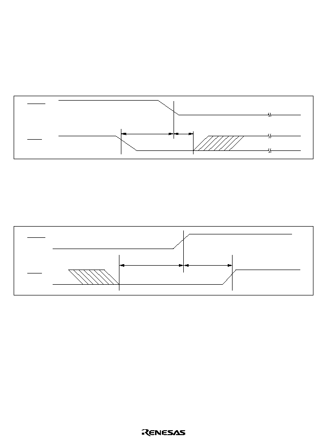
934
Appendix E Timing of Transition to and Recovery from
Hardware Standby Mode
Timing of Transition to Hardware Standby Mode
1. To retain RAM contents with the RAME bit set to 1 in SYSCR, drive the
RES signal low 10
system clock cycles before the
STBY signal goes low, as shown below. RES must remain low
until
STBY goes low (minimum delay from STBY low to RES high: 0 ns).
t
1
10t
cyc
t
2
0 ns
STBY
RES
2. To retain RAM contents with the RAME bit cleared to 0 in SYSCR,
RES does not have to be
driven low as in (1).
Timing of Recovery from Hardware Standby Mode: Drive the
RES signal low approximately
100 ns before
STBY goes high.
STBY
RES
t
100 ns
t
OSC

935
Appendix F Product Code Lineup
Product Type
Product Code
Mark Code
Package
(Hitachi Package Code)
H8/3069F
On-chip flash
HD64F3069F
HD64F3069F
100-pin QFP (FP-100B)
memory
HD64F3069TE
HD64F3069TE
100-pin TQFP (TFP-100B)
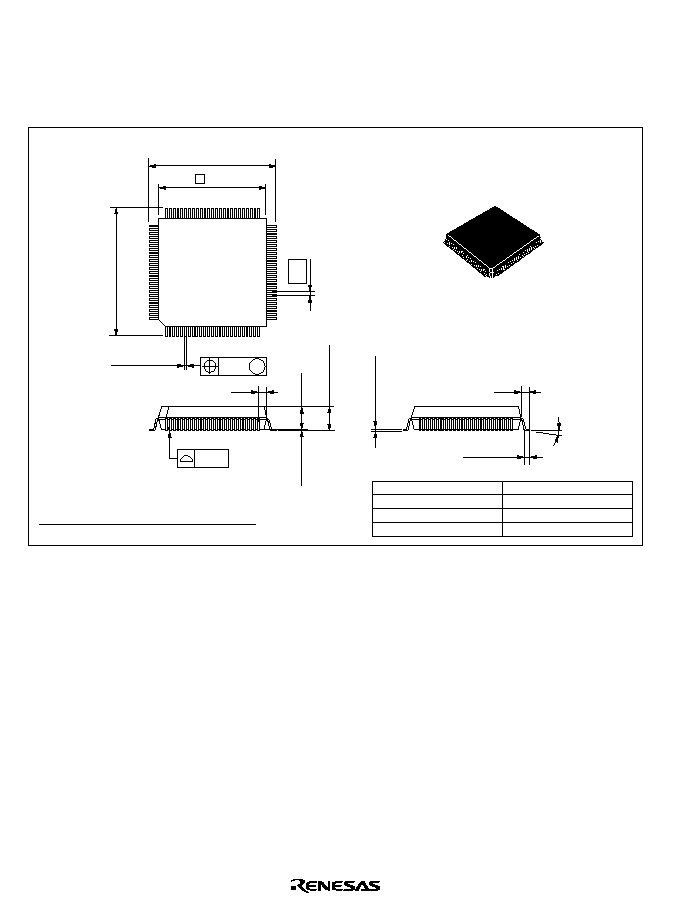
936
Appendix G Package Dimensions
Figures G.1 show the FP-100B package dimensions of the H8/3069F. Figure G.2 shows the TFP-
100B package dimensions.
Hitachi Code
JEDEC
JEITA
Mass (reference value)
FP-100B
--
Conforms
1.2 g
*
Dimension including the plating thickness
Base material dimension
0.10
16.0
�
0.3
1.0
0.5
�
0.2
16.0
�
0.3
3.05 Max
75
51
50
26
1
25
76
100
14
0
�
� 8
�
0.5
0.08 M
*
0.22
�
0.05
2.70
*
0.17
�
0.05
0.12
+0.13 �0.12
1.0
0.20
�
0.04
0.15
�
0.04
As of July, 2002
Unit: mm
Figure G.1 Package Dimensions (FP-100B)
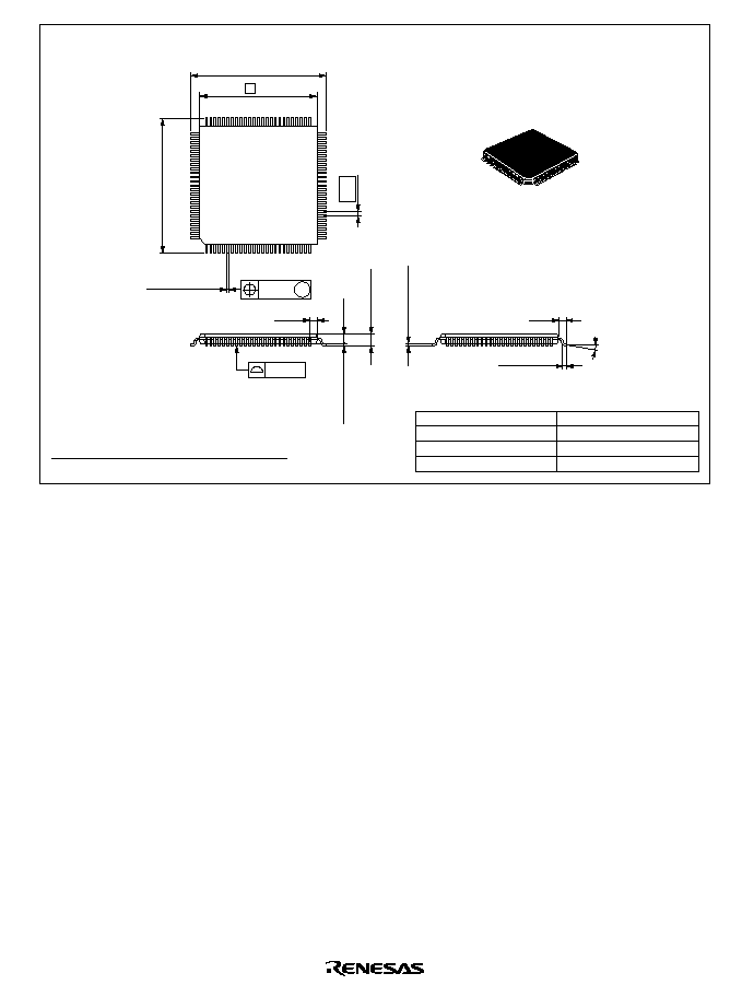
937
Hitachi Code
JEDEC
JEITA
Mass (reference value)
TFP-100B
--
Conforms
0.5 g
*
Dimension including the plating thickness
Base material dimension
16.0
�
0.2
14
0.08
0.10
0.5
�
0.1
16.0
�
0.2
0.5
0.10
�
0.10
1.20 Max
*
0.17
�
0.05
0
�
� 8
�
75
51
1
25
76
100
26
50
M
*
0.22
�
0.05
1.0
1.00
1.0
0.20
�
0.04
0.15
�
0.04
As of July, 2002
Unit: mm
Figure G.2 Package Dimensions (TFP-100B)

938
Appendix H Comparison of H8/300H Series Product
Specifications
H.1
Differences between H8/3069F, H8/3067 Series and H8/3062 Series,
H8/3048 Series, H8/3007 and H8/3006, and H8/3002
Item
H8/3069F
H8/3067 Series,
H8/3062 Series
H8/3048
Series
H8/3007 and
H8/3006
H8/3002
1
Operating
mode
Mode 5
16 Mbytes ROM
enabled expanded
mode
16 Mbytes ROM
enabled expanded
mode
1 Mbyte ROM
enabled
expanded
mode
Mode 6
--
64 kbytes single-chip
mode
16 Mbyte ROM
enabled
expanded
mode
2
Interrupt
controller
Internal
interrupt
sources
36
36 (H8/3067)
27 (H8/3062)
30
36
30
3
Bus controller Burst ROM
interface
Yes
Yes (H8/3067)
No (H8/3062)
No
Yes
No
Idle cycle
insertion
function
Yes
Yes
No
Yes
No
Wait mode 2 modes
2 modes
4 modes
2 modes
4 modes
Wait state
number
setting
Per area
Per area
Common
to all areas
Per area
Common
to all areas
Address
output
method
Choice of address
update fixed
Choice of address
update mode (fixed in
H8/3067F-ZTAT and
H8/3062F-ZTAT)
Fixed
Fixed
Fixed
4
DRAM
interface
Connect-
able areas
Area 2/3/4/5
Area 2/3/4/5
(H8/3067 only)
Area 3
Area 2/3/4/5
Area 3

939
Item
H8/3069F
H8/3067 Series,
H8/3062 Series
H8/3048
Series
H8/3007,
H8/3006
H8/3002
4
DRAM
interface
Precharge
cycle
insertion
function
Yes
Yes (H8/3067 only)
No
Yes
No
Fast page
mode
Yes
Yes (H8/3067 only)
No
Yes
No
Address
shift
amount
8 bit/9 bit/10 bit
8 bit/9 bit/10 bit
(H8/3067 only)
8 bit/9 bit
8-bit/9-bit/10-bit
8-bit/9-bit
5
Timer functions
16-bit
timers
8-bit
timers
16-bit
timers
8-bit
timers
ITU
16-bit
timers
8-bit timers ITU
Number of
channels
16 bits
�
3 8 bits
�
4
(16 bits
�
2)
16 bits
�
3 8 bits
�
4
(16 bits
�
2)
16 bits
�
5 16 bits x 3 8 bits x 4
(16 bits x 2)
16 bits x 5
Pulse
output
6 pins
4 pins
(2 pins)
6 pins
4 pins
(2 pins)
12 pins
6 pins
4 pins
(2 pins)
12 pins
Input
capture
6
2
6
2
10
6
2
10
External
clock
4 systems
(select-
able)
4 systems
(fixed)
4 systems
(select-
able)
4 systems
(fixed)
4 systems
(select-
able)
4 systems
(select-
able)
4 systems
(fixed)
4 systems
(select-
able)
Internal
clock
,
/2,
/4,
/8
/8,
/64,
/8192
,
/2,
/4,
/8
/8,
/64,
/8192
,
/2,
/4,
/8
,
/2,
/4,
/8
/8,
/64,
/8192
,
/2,
/4,
/8
Comple-
mentary
PWM
function
No
No
No
No
Yes
No
No
Yes
Reset-
synchro-
nous PWM
function
No
No
No
No
Yes
No
No
Yes
Buffer
operation
No
No
No
No
Yes
No
No
Yes
Output
initializa-
tion
function
Yes
No
Yes
No
No
Yes
No
No

940
Item
H8/3069F
H8/3067 Series,
H8/3062 Series
H8/3048
Series
H8/3007,
H8/3006
H8/3002
5
Timer
functions
PWM
output
3
4 (2)
3
4 (2)
5
3
4 (2)
5
DMAC
activation
3 channels No
3 channels
(H8/3067
only)
No
4 channels 3 channels No
4 channels
A/D
conversion
activation
No
Yes
No
Yes
No
No
Yes
No
Interrupt
sources
3 sources
�
3
8 sources
3 sources
�
3
8 sources
3 sources
�
5
3 sources
�
3
8 sources
3 sources
�
5
6
TPC
Time base 3 kinds, 16-bit timer
base
3 kinds, 16-bit timer
base
4 kinds,
ITU base
3 kinds, 16-bit timer
base
4 kinds,
ITU base
7
WDT
Reset
signal
external
output
function
No
Yes (except
products
with on-
chip flash
memory)
Yes
Yes
Yes
Yes
8
SCI
Number of
channels
3 channels
3 channels (H8/3067)
2 channels (H8/3062)
2 channels 3 channels
2 channels
Smart card
interface
Supported on all
channels
Supported on all
channels
Supported
on SCI0
only
Supported on all
channels
No

941
Item
H8/3069F
H8/3067 Series,
H8/3062 Series
H8/3048
Series
H8/3007, H8/3006
H8/3002
9
A/D converter Conversion
start trigger
input
External trigger/8-bit
timer compare match
External trigger/8-bit
timer compare match
External
trigger
External trigger/8-bit
timer compare match
External
trigger
Conversion
state
70/134
70/134
134/266
70/134
134/266
10
Pin
control
pin
/input port multiplexing
/input port multiplexing
output
only
/input port
multiplexing
output
only
A
20
in 16
MB ROM
enabled
expanded
mode
A
20
/ I/O port
multiplexing
A
20
/ I/O port
multiplexing
A
20
output
Address
bus,
AS
,
RD
,
HWR
,
LWR
,
CS
7
�
CS
0
,
RFSH
in
software
standby
state
High-level output/high-
impedance selectable
High-level output/high-
impedance selectable
(
RFSH
: H8/3067 only)
High-level
output
(except
CS
0
)
Low-level
output
(
CS
0
)
High-level output/high-
impedance selectable
High-level
output
(except
CS
0
)
Low-level
output
(
CS
0
)
CS
7
�
CS
0
in bus-
released
state
High-impedance
High-impedance
High-level
output
High-impedance
High-level
output
11
Flash memory
functions
Program/
erase
voltage
12 V application
unnecessary.
Single-power-supply
programming.
12 V application
unnecessary.
Single-power-supply
programming.
12 V
application
from off-
chip
Block
divisions
16 blocks
8 blocks (12 blocks in
H8/3064F-ZTAT)
16 blocks
Boot mode Yes
Yes
Yes
User
program
mode
Yes
Yes
Yes
User boot
mode
Yes
No
No

942
H.2
Comparison of Pin Functions of 100-Pin Package Products
(FP-100B, TFP-100B)
Table H.1
Pin Arrangement of Each Product (FP-100B, TFP-100B)
ROMless Version
Pin No.
H8/3069F
H8/3067
Series
H8/3062
Series
H8/3048
Series
H8/3042
Series
H8/3007,
H8/3006
H8/3002
1
VCL
VCC
VCC/VCL
*
2
VCC
VCC
VCC
VCC
2
PB
0
/TP
8
/
TMO
0
/
CS
7
PB
0
/TP
8
/
TMO
0
/
CS
7
PB
0
/TP
8
/
TMO
0
/
CS
7
PB
0
/TP
8
/
TIOCA
3
PB
0
/TP
8
/
TIOCA
3
PB
0
/TP
8
/
TMO
0
/
CS
7
PB
0
/TP
8
/TIO
CA3
3
PB
1
/TP
9
/
TMIO
1
/
DREQ
0
/
CS
6
PB
1
/TP
9
/
TMIO
1
/
DREQ
0
/
CS
6
PB
1
/TP
9
/
TMIO
1
/
CS
6
PB
1
/TP
9
/
TIOCB
3
PB
1
/TP
9
/
TIOCB
3
PB
1
/TP
9
/
TMIO
1
/
DREQ
0
/
CS
6
PB
1
/TP
9
/TIO
CB3
4
PB
2
/TP
10
/TM
O
2
/
CS
5
PB
2
/TP
10
/TM
O
2
/
CS
5
PB
2
/TP
10
/TM
O
2
/
CS
5
PB
2
/TP
10
/
TIOCA
4
PB
2
/TP
10
/
TIOCA
4
PB
2
/TP
10
/
TMO
2
/
CS
5
PB
2
/TP
10
/
TIOCA4
5
PB
3
/TP
11
/
TMIO
3
/
DREQ
1
/
CS
4
PB
3
/TP
11
/
TMIO
3
/
DREQ
1
/
CS
4
PB
3
/TP
11
/
TMIO
3
/
CS
4
PB
3
/TP
11
/
TIOCB
4
PB
3
/TP
11
/
TIOCB
4
PB
3
/TP
11
/
TMIO
3
/
DREQ
1
/
CS
4
PB
3
/TP
11
/
TIOCB4
6
PB
4
/TP
12
/
UCAS
PB
4
/TP
12
/
UCAS
PB
4
/TP
12
PB
4
/TP
12
/
TOCXA
4
PB
4
/TP
12
/
TOCXA
4
PB
4
/TP
12
/
UCAS
PB
4
/TP
12
/
TOCXA
4
7
PB
5
/TP
13
/
LCAS
/
SCK
2
PB
5
/TP
13
/
LCAS
/
SCK
2
PB
5
/TP
13
PB
5
/TP
13
/
TOCXB
4
PB
5
/TP
13
/
TOCXB
4
PB
5
/TP
13
/
LCAS
/SCK
2
PB
5
/TP
13
/
TOCXB
4
8
PB
6
/TP
14
/
TxD
2
PB
6
/TP
14
/
TxD
2
PB
6
/TP
14
PB
6
/TP
14
/
DREQ
0
/
CS
7
PB
6
/TP
14
/
DREQ
0
PB
6
/TP
14
/
TxD
2
PB
6
/TP
14
/
DREQ
0
9
PB
7
/TP
15
/
RxD
2
PB
7
/TP
15
/
RxD
2
PB
7
/TP
15
PB
7
/TP
15
/
DREQ
1
/
ADTRG
PB
7
/TP
15
/
DREQ
1
/
ADTRG
PB
7
/TP
15
/
RxD
2
PB
7
/TP
16
/
DREQ
1
/
ADTRG
10
FWE
RESO
/
FWE
*
1
RESO
/
FWE
*
1
RESO
/V
PP
RESO
RESO
RESO
11
Vss
Vss
Vss
Vss
Vss
Vss
Vss
12
P9
0
/TxD
0
P9
0
/TxD
0
P9
0
/TxD
0
P9
0
/TxD
0
P9
0
/TxD
0
P9
0
/TxD
0
P9
0
/TxD
0
13
P9
1
/TxD
1
P9
1
/TxD
1
P9
1
/TxD
1
P9
1
/TxD
1
P9
1
/TxD
1
P9
1
/TxD
1
P9
1
/TxD
1
14
P9
2
/RxD
0
P9
2
/RxD
0
P9
2
/RxD
0
P9
2
/RxD
0
P9
2
/RxD
0
P9
2
/RxD
0
P9
2
/RxD
0
15
P9
3
/RxD
1
P9
3
/RxD
1
P9
3
/RxD
1
P9
3
/RxD
1
P9
3
/RxD
1
P9
3
/RxD
1
P9
3
/RxD
1
16
P9
4
/SCK
0
/
IRQ
4
P9
4
/SCK
0
/
IRQ
4
P9
4
/SCK
0
/
IRQ
4
P9
4
/SCK
0
/
IRQ
4
P9
4
/SCK
0
/
IRQ
4
P9
4
/SCK
0
/
IRQ
4
P9
4
/SCK
0
/
IRQ
4
17
P9
5
/SCK
1
/
IRQ
5
P9
5
/SCK
1
/
IRQ
5
P9
5
/SCK
1
/
IRQ
5
P9
5
/SCK
1
/
IRQ
5
P9
5
/SCK
1
/
IRQ
5
P9
5
/SCK
1
/
IRQ
5
P9
5
/SCK
1
/
IRQ
5

943
ROMless Version
Pin No.
H8/3069F
H8/3067
Series
H8/3062
Series
H8/3048
Series
H8/3042
Series
H8/3007,
H8/3006
H8/3002
18
P4
0
/D
0
P4
0
/D
0
P4
0
/D
0
P4
0
/D
0
P4
0
/D
0
P4
0
/D
0
P4
0
/D
0
19
P4
1
/D
1
P4
1
/D
1
P4
1
/D
1
P4
1
/D
1
P4
1
/D
1
P4
1
/D
1
P4
1
/D
1
20
P4
2
/D
2
P4
2
/D
2
P4
2
/D
2
P4
2
/D
2
P4
2
/D
2
P4
2
/D
2
P4
2
/D
2
21
P4
3
/D
3
P4
3
/D
3
P4
3
/D
3
P4
3
/D
3
P4
3
/D
3
P4
3
/D
3
P4
3
/D
3
22
Vss
Vss
Vss
Vss
Vss
Vss
Vss
23
P4
4
/D
4
P4
4
/D
4
P4
4
/D
4
P4
4
/D
4
P4
4
/D
4
P4
4
/D
4
P4
4
/D
4
24
P4
5
/D
5
P4
5
/D
5
P4
5
/D
5
P4
5
/D
5
P4
5
/D
5
P4
5
/D
5
P4
5
/D
5
25
P4
6
/D
6
P4
6
/D
6
P4
6
/D
6
P4
6
/D
6
P4
6
/D
6
P4
6
/D
6
P4
6
/D
6
26
P4
7
/D
7
P4
7
/D
7
P4
7
/D
7
P4
7
/D
7
P4
7
/D
7
P4
7
/D
7
P4
7
/D
7
27
P3
0
/D
8
P3
0
/D
8
P3
0
/D
8
P3
0
/D
8
P3
0
/D
8
D
8
D
8
28
P3
1
/D
9
P3
1
/D
9
P3
1
/D
9
P3
1
/D
9
P3
1
/D
9
D
9
D
9
29
P3
2
/D
10
P3
2
/D
10
P3
2
/D
10
P3
2
/D
10
P3
2
/D
10
D
10
D
10
30
P3
3
/D
11
P3
3
/D
11
P3
3
/D
11
P3
3
/D
11
P3
3
/D
11
D
11
D
11
31
P3
4
/D
12
P3
4
/D
12
P3
4
/D
12
P3
4
/D
12
P3
4
/D
12
D
12
D
12
32
P3
5
/D
13
P3
5
/D
13
P3
5
/D
13
P3
5
/D
13
P3
5
/D
13
D
13
D
13
33
P3
6
/D
14
P3
6
/D
14
P3
6
/D
14
P3
6
/D
14
P3
6
/D
14
D
14
D
14
34
P3
7
/D
15
P3
7
/D
15
P3
7
/D
15
P3
7
/D
15
P3
7
/D
15
D
15
D
15
35
Vcc
Vcc
Vcc
Vcc
Vcc
Vcc
Vcc
36
P1
0
/A
0
P1
0
/A
0
P1
0
/A
0
P1
0
/A
0
P1
0
/A
0
A
0
A
0
37
P1
1
/A
1
P1
1
/A
1
P1
1
/A
1
P1
1
/A
1
P1
1
/A
1
A
1
A
1
38
P1
2
/A
2
P1
2
/A
2
P1
2
/A
2
P1
2
/A
2
P1
2
/A
2
A
2
A
2
39
P1
3
/A
3
P1
3
/A
3
P1
3
/A
3
P1
3
/A
3
P1
3
/A
3
A
3
A
3
40
P1
4
/A
4
P1
4
/A
4
P1
4
/A
4
P1
4
/A
4
P1
4
/A
4
A
4
A
4
41
P1
5
/A
5
P1
5
/A
5
P1
5
/A
5
P1
5
/A
5
P1
5
/A
5
A
5
A
5
42
P1
6
/A
6
P1
6
/A
6
P1
6
/A
6
P1
6
/A
6
P1
6
/A
6
A
6
A
6
43
P1
7
/A
7
P1
7
/A
7
P1
7
/A
7
P1
7
/A
7
P1
7
/A
7
A
7
A
7
44
Vss
Vss
Vss
Vss
Vss
Vss
Vss
45
P2
0
/A
8
P2
0
/A
8
P2
0
/A
8
P2
0
/A
8
P2
0
/A
8
A
8
A
8
46
P2
1
/A
9
P2
1
/A
9
P2
1
/A
9
P2
1
/A
9
P2
1
/A
9
A
9
A
9
47
P2
2
/A
10
P2
2
/A
10
P2
2
/A
10
P2
2
/A
10
P2
2
/A
10
A
10
A
10
48
P2
3
/A
11
P2
3
/A
11
P2
3
/A
11
P2
3
/A
11
P2
3
/A
11
A
11
A
11
49
P2
4
/A
12
P2
4
/A
12
P2
4
/A
12
P2
4
/A
12
P2
4
/A
12
A
12
A
12
50
P2
5
/A
13
P2
5
/A
13
P2
5
/A
13
P2
5
/A
13
P2
5
/A
13
A
13
A
13
51
P2
6
/A
14
P2
6
/A
14
P2
6
/A
14
P2
6
/A
14
P2
6
/A
14
A
14
A
14

944
ROMless Version
Pin No.
H8/3069F
H8/3067
Series
H8/3062
Series
H8/3048
Series
H8/3042
Series
H8/3007,
H8/3006
H8/3002
52
P2
7
/A
15
P2
7
/A
15
P2
7
/A
15
P2
7
/A
15
P2
7
/A
15
A
15
A
15
53
P5
0
/A
16
P5
0
/A
16
P5
0
/A
16
P5
0
/A
16
P5
0
/A
16
A
16
A
16
54
P5
1
/A
17
P5
1
/A
17
P5
1
/A
17
P5
1
/A
17
P5
1
/A
17
A
17
A
17
55
P5
2
/A
18
P5
2
/A
18
P5
2
/A
18
P5
2
/A
18
P5
2
/A
18
A
18
A
18
56
P5
3
/A
19
P5
3
/A
19
P5
3
/A
19
P5
3
/A
19
P5
3
/A
19
A
19
A
19
57
Vss
Vss
Vss
Vss
Vss
Vss
Vss
58
P6
0
/
WAIT
P6
0
/
WAIT
P6
0
/
WAIT
P6
0
/
WAIT
P6
0
/
WAIT
P6
0
/
WAIT
P6
0
/
WAIT
59
P6
1
/
BREQ
P6
1
/
BREQ
P6
1
/
BREQ
P6
1
/
BREQ
P6
1
/
BREQ
P6
1
/
BREQ
P6
1
/
BREQ
60
P6
2
/
BACK
P6
2
/
BACK
P6
2
/
BACK
P6
2
/
BACK
P6
2
/
BACK
P6
2
/
BACK
P6
2
/
BACK
61
P6
7
/
P6
7
/
P6
7
/
P6
7
/
62
STBY
STBY
STBY
STBY
STBY
STBY
STBY
63
RES
RES
RES
RES
RES
RES
RES
64
NMI
NMI
NMI
NMI
NMI
NMI
NMI
65
Vss
Vss
Vss
Vss
Vss
Vss
NMI
66
EXTAL
EXTAL
EXTAL
EXTAL
EXTAL
EXTAL
EXTAL
67
XTAL
XTAL
XTAL
XTAL
XTAL
XTAL
XTAL
68
Vcc
Vcc
Vcc
Vcc
Vcc
Vcc
Vcc
69
P6
3
/
AS
P6
3
/
AS
P6
3
/
AS
P6
3
/
AS
P6
3
/
AS
AS
AS
70
P6
4
/
RD
P6
4
/
RD
P6
4
/
RD
P6
4
/
RD
P6
4
/
RD
RD
RD
71
P6
5
/
HWR
P6
5
/
HWR
P6
5
/
HWR
P6
5
/
HWR
P6
5
/
HWR
HWR
HWR
72
P6
6
/
LWR
P6
6
/
LWR
P6
6
/
LWR
P6
6
/
LWR
P6
6
/
LWR
LWR
LWR
73
MD
0
MD
0
MD
0
MD
0
MD
0
MD
0
MD
0
74
MD
1
MD
1
MD
1
MD
1
MD
1
MD
1
MD
1
75
MD
2
MD
2
MD
2
MD
2
MD
2
MD
2
MD
2
76
AVcc
AVcc
AVcc
AVcc
AVcc
AVcc
AVcc
77
V
REF
V
REF
V
REF
V
REF
V
REF
V
REF
V
REF
78
P7
0
/AN
0
P7
0
/AN
0
P7
0
/AN
0
P7
0
/AN
0
P7
0
/AN
0
P7
0
/AN
0
P7
0
/AN
0
79
P7
1
/AN
1
P7
1
/AN
1
P7
1
/AN
1
P7
1
/AN
1
P7
1
/AN
1
P7
1
/AN
1
P7
1
/AN
1
80
P7
2
/AN
2
P7
2
/AN
2
P7
2
/AN
2
P7
2
/AN
2
P7
2
/AN
2
P7
2
/AN
2
P7
2
/AN
2
81
P7
3
/AN
3
P7
3
/AN
3
P7
3
/AN
3
P7
3
/AN
3
P7
3
/AN
3
P7
3
/AN
3
P7
3
/AN
3
82
P7
4
/AN
4
P7
4
/AN
4
P7
4
/AN
4
P7
4
/AN
4
P7
4
/AN
4
P7
4
/AN
4
P7
4
/AN
4
83
P7
5
/AN
5
P7
5
/AN
5
P7
5
/AN
5
P7
5
/AN
5
P7
5
/AN
5
P7
5
/AN
5
P7
5
/AN
5
84
P7
6
/AN
6
/DA
0
P7
6
/AN
6
/DA
0
P7
6
/AN
6
/DA
0
P7
6
/AN
6
/DA
0
P7
6
/AN
6
/DA
0
P7
6
/AN
6
/DA
0
P7
6
/AN
6
85
P7
7
/AN
7
/DA
1
P7
7
/AN
7
/DA
1
P7
7
/AN
7
/DA
1
P7
7
/AN
7
/DA
1
P7
7
/AN
7
/DA
1
P7
7
/AN
7
P7
7
/AN
7

945
ROMless Version
Pin No.
H8/3069F
H8/3067
Series
H8/3062
Series
H8/3048
Series
H8/3042
Series
H8/3007,
H8/3006
H8/3002
86
AVss
AVss
AVss
AVss
AVss
AVss
AVss
87
P8
0
/
RFSH
/
IRQ
0
P8
0
/
RFSH
/
IRQ
0
P8
0
/
IRQ
0
P8
0
/
RFSH
/
IRQ
0
P8
0
/
RFSH
/
IRQ
0
P8
0
/
RFSH
/
IRQ
0
P8
0
/
RFSH
/
IRQ
0
88
P8
1
/
CS
3
/
IRQ
1
P8
1
/
CS
3
/
IRQ
1
P8
1
/
CS
3
/
IRQ
1
P8
1
/
CS
3
/
IRQ
1
P8
1
/
CS
3
/
IRQ
1
P8
1
/
CS
3
/
IRQ
1
P8
1
/
CS
3
/
IRQ
1
89
P8
2
/
CS
2
/
IRQ
2
P8
2
/
CS
2
/
IRQ
2
P8
2
/
CS
2
/
IRQ
2
P8
2
/
CS
2
/
IRQ
2
P8
2
/
CS
2
/
IRQ
2
P8
2
/
CS
2
/
IRQ
2
P8
2
/
CS
2
/
IRQ
2
90
P8
3
/
CS
1
/
IRQ
3
/
ADTRG
P8
3
/
CS
1
/
IRQ
3
/
ADTRG
P8
3
/
CS
1
/
IRQ
3
/
ADTRG
P8
3
/
CS
1
/
IRQ
3
P8
3
/
CS
1
/
IRQ
3
P8
3
/
CS
1
/
IRQ
3
/
ADTRG
P8
3
/
CS
1
/
IRQ
3
91
P8
4
/
CS
0
P8
4
/
CS
0
P8
4
/
CS
0
P8
4
/
CS
0
P8
4
/
CS
0
P8
4
/
CS
0
P8
4
/
CS
0
92
Vss
Vss
Vss
Vss
Vss
Vss
Vss
93
PA
0
/TP
0
/
TEND
0
/
TCLKA
PA
0
/TP
0
/
TEND
0
/
TCLKA
PA
0
/TP
0
/
TCLKA
PA
0
/TP
0
/
TEND
0
/
TCLKA
PA
0
/TP
0
/
TEND
0
/
TCLKA
PA
0
/TP
0
/
TEND
0
/
TCLKA
PA
0
/TP
0
/
TEND
0
/
TCLKA
94
PA
1
/TP
1
/
TEND
1
/
TCLKB
PA
1
/TP
1
/
TEND
1
/
TCLKB
PA
1
/TP
1
/
TCLKB
PA
1
/TP
1
/
TEND
1
/
TCLKB
PA
1
/TP
1
/
TEND
1
/
TCLKB
PA
1
/TP
1
/
TEND
1
/
TCLKB
PA
1
/TP
1
/
TEND
1
/
TCLKB
95
PA
2
/TP
2
/
TIOCA
0
/
TCLKC
PA
2
/TP
2
/
TIOCA
0
/
TCLKC
PA
2
/TP
2
/
TIOCA
0
/
TCLKC
PA
2
/TP
2
/
TIOCA
0
/
TCLKC
PA
2
/TP
2
/
TIOCA
0
/
TCLKC
PA
2
/TP
2
/
TIOCA
0
/
TCLKC
PA
2
/TP
2
/
TIOCA
0
/
TCLKC
96
PA
3
/TP
3
/
TIOCB
0
/
TCLKD
PA
3
/TP
3
/
TIOCB
0
/
TCLKD
PA
3
/TP
3
/
TIOCB
0
/
TCLKD
PA
3
/TP
3
/
TIOCB
0
/
TCLKD
PA
3
/TP
3
/
TIOCB
0
/
TCLKD
PA
3
/TP
3
/
TIOCB
0
/
TCLKD
PA
3
/TP
3
/
TIOCB
0
/
TCLKD
97
PA
4
/TP
4
/
TIOCA
1
/
A
23
PA
4
/TP
4
/
TIOCA
1
/
A
23
PA
4
/TP
4
/
TIOCA
1
/
A
23
PA
4
/TP
4
/
TIOCA
1
/
CS
6
/A
23
PA
4
/TP
4
/
TIOCA
1
/
A
23
PA
4
/TP
4
/
TIOCA
1
/
A
23
PA
4
/TP
4
/
TIOCA
1
/
A
23
98
PA
5
/TP
5
/
TIOCB
1
/
A
22
PA
5
/TP
5
/
TIOCB
1
/
A
22
PA
5
/TP
5
/
TIOCB
1
/
A
22
PA
5
/TP
5
/
TIOCB
1
/
CS
5
/A
22
PA
5
/TP
5
/
TIOCB
1
/
A
22
PA
5
/TP
5
/
TIOCB
1
/
A
22
PA
5
/TP
5
/
TIOCB
1
/
A
22
99
PA
6
/TP
6
/
TIOCA
2
/
A
21
PA
6
/TP
6
/
TIOCA
2
/
A
21
PA
6
/TP
6
/
TIOCA
2
/
A
21
PA
6
/TP
6
/
TIOCA
2
/
CS
4
/A
21
PA
6
/TP
6
/
TIOCA
2
/
A
21
PA
6
/TP
6
/
TIOCA
2
/
A
21
PA
6
/TP
6
/
TIOCA
2
/
A
21
100
PA
7
/TP
7
/
TIOCB
2
/A
20
PA
7
/TP
7
/
TIOCB
2
/A
20
PA
7
/TP
7
/
TIOCB
2
/A
20
PA
7
/TP
7
/
TIOCB
2
/A
20
PA
7
/TP
7
/
TIOCB
2
/A
20
PA
7
/TP
7
/
TIOCB
2
/A
20
PA
7
/TP
7
/
TIOCB
2
/A
20
Notes:
*
1 Functions as
RESO
in the mask ROM versions, and as FWE in the flash memory and
flash memory R versions.
*
2 Functions as the V
CL
pin in the 5-V products of the H8/3064F-ZTAT and H8/3062F-
ZTAT A-mask versions, and requires an external capacitor (0.1
�
F).

946

H8/3069 F-ZTAT Hardware Manual
Publication Date: 1st Edition, March 2002
2nd Edition, December 2002
Published by:
Business Operation3 Division
Semiconductor & Integrated Circuits
Hitachi, Ltd.
Edited by:
Technical Documentation Group
Hitachi Kodaira Semiconductor Co., Ltd.
Copyright � Hitachi, Ltd., 2002. All rights reserved. Printed in Japan.
Document Outline
- Cover
- Cautions
- General Precautions on Handling of Product
- Preface
- Revisions and Additions in this Edition
- Contents
- Section 1 Overview
- 1.1 Overview
- 1.2 Block Diagram
- 1.3 Pin Description
- 1.3.1 Pin Arrangement
- 1.3.2 Pin Functions
- 1.3.3 Pin Assignments in Each Mode
- Section 2 CPU
- 2.1 Overview
- 2.1.1 Features
- 2.1.2 Differences from H8/300 CPU
- 2.2 CPU Operating Modes
- 2.3 Address Space
- 2.4 Register Configuration
- 2.4.1 Overview
- 2.4.2 General Registers
- 2.4.3 Control Registers
- 2.4.4 Initial CPU Register Values
- 2.5 Data Formats
- 2.5.1 General Register Data Formats
- 2.5.2 Memory Data Formats
- 2.6 Instruction Set
- 2.6.1 Instruction Set Overview
- 2.6.2 Instructions and Addressing Modes
- 2.6.3 Tables of Instructions Classified by Function
- 2.6.4 Basic Instruction Formats
- 2.6.5 Notes on Use of Bit Manipulation Instructions
- 2.7 Addressing Modes and Effective Address Calculation
- 2.7.1 Addressing Modes
- 2.7.2 Effective Address Calculation
- 2.8 Processing States
- 2.8.1 Overview
- 2.8.2 Program Execution State
- 2.8.3 Exception-Handling State
- 2.8.4 Exception-Handling Sequences
- 2.8.5 Bus-Released State
- 2.8.6 Reset State
- 2.8.7 Power-Down State
- 2.9 Basic Operational Timing
- 2.9.1 Overview
- 2.9.2 On-Chip Memory Access Timing
- 2.9.3 On-Chip Supporting Module Access Timing
- 2.9.4 Access to External Address Space
- Section 3 MCU Operating Modes
- 3.1 Overview
- 3.1.1 Operating Mode Selection
- 3.1.2 Register Configuration
- 3.2 Mode Control Register (MDCR)
- 3.3 System Control Register (SYSCR)
- 3.4 Operating Mode Descriptions
- 3.4.1 Mode 1
- 3.4.2 Mode 2
- 3.4.3 Mode 3
- 3.4.4 Mode 4
- 3.4.5 Mode 5
- 3.4.6 Mode 7
- 3.5 Pin Functions in Each Operating Mode
- 3.6 Memory Map in Each Operating Mode
- 3.6.1 Note on Reserved Areas
- Section 4 Exception Handling
- 4.1 Overview
- 4.1.1 Exception Handling Types and Priority
- 4.1.2 Exception Handling Operation
- 4.1.3 Exception Vector Table
- 4.2 Reset
- 4.2.1 Overview
- 4.2.2 Reset Sequence
- 4.2.3 Interrupts after Reset
- 4.3 Interrupts
- 4.4 Trap Instruction
- 4.5 Stack Status after Exception Handling
- 4.6 Notes on Stack Usage
- Section 5 Interrupt Controller
- 5.1 Overview
- 5.1.1 Features
- 5.1.2 Block Diagram
- 5.1.3 Pin Configuration
- 5.1.4 Register Configuration
- 5.2 Register Descriptions
- 5.2.1 System Control Register (SYSCR)
- 5.2.2 Interrupt Priority Registers A and B (IPRA, IPRB)
- 5.2.3 IRQ Status Register (ISR)
- 5.2.4 IRQ Enable Register (IER)
- 5.2.5 IRQ Sense Control Register (ISCR)
- 5.3 Interrupt Sources
- 5.3.1 External Interrupts
- 5.3.2 Internal Interrupts
- 5.3.3 Interrupt Vector Table
- 5.4 Interrupt Operation
- 5.4.1 Interrupt Handling Process
- 5.4.2 Interrupt Sequence
- 5.4.3 Interrupt Response Time
- 5.5 Usage Notes
- 5.5.1 Contention between Interrupt and Interrupt-Disabling Instruction
- 5.5.2 Instructions that Inhibit Interrupts
- 5.5.3 Interrupts during EEPMOV Instruction Execution
- Section 6 Bus Controller
- 6.1 Overview
- 6.1.1 Features
- 6.1.2 Block Diagram
- 6.1.3 Pin Configuration
- 6.1.4 Register Configuration
- 6.2 Register Descriptions
- 6.2.1 Bus Width Control Register (ABWCR)
- 6.2.2 Access State Control Register (ASTCR)
- 6.2.3 Wait Control Registers H and L (WCRH, WCRL)
- 6.2.4 Bus Release Control Register (BRCR)
- 6.2.5 Bus Control Register (BCR)
- 6.2.6 Chip Select Control Register (CSCR)
- 6.2.7 DRAM Control Register A (DRCRA)
- 6.2.8 DRAM Control Register B (DRCRB)
- 6.2.9 Refresh Timer Control/Status Register (RTMCSR)
- 6.2.10 Refresh Timer Counter (RTCNT)
- 6.2.11 Refresh Time Constant Register (RTCOR)
- 6.2.12 Address Control Register (ADRCR)
- 6.3 Operation
- 6.3.1 Area Division
- 6.3.2 Bus Specifications
- 6.3.3 Memory Interfaces
- 6.3.4 Chip Select Signals
- 6.3.5 Address Output Method
- 6.4 Basic Bus Interface
- 6.4.1 Overview
- 6.4.2 Data Size and Data Alignment
- 6.4.3 Valid Strobes
- 6.4.4 Memory Areas
- 6.4.5 Basic Bus Control Signal Timing
- 6.4.6 Wait Control
- 6.5 DRAM Interface
- 6.5.1 Overview
- 6.5.2 DRAM Space and RAS Output Pin Settings
- 6.5.3 Address Multiplexing
- 6.5.4 Data Bus
- 6.5.5 Pins Used for DRAM Interface
- 6.5.6 Basic Timing
- 6.5.7 Precharge State Control
- 6.5.8 Wait Control
- 6.5.9 Byte Access Control and CAS Output Pin
- 6.5.10 Burst Operation
- 6.5.11 Refresh Control
- 6.5.12 Examples of Use
- 6.5.13 Usage Notes
- 6.6 Interval Timer
- 6.7 Interrupt Sources
- 6.8 Burst ROM Interface
- 6.8.1 Overview
- 6.8.2 Basic Timing
- 6.8.3 Wait Control
- 6.9 Idle Cycle
- 6.9.1 Operation
- 6.9.2 Pin States in Idle Cycle
- 6.10 Bus Arbiter
- 6.11 Register and Pin Input Timing
- 6.11.1 Register Write Timing
- 6.11.2 BREQ Pin Input Timing
- Section 7 DMA Controller
- 7.1 Overview
- 7.1.1 Features
- 7.1.2 Block Diagram
- 7.1.3 Functional Overview
- 7.1.4 Input/Output Pins
- 7.1.5 Register Configuration
- 7.2 Register Descriptions (1) (Short Address Mode)
- 7.2.1 Memory Address Registers (MAR)
- 7.2.2 I/O Address Registers (IOAR)
- 7.2.3 Execute Transfer Count Registers (ETCR)
- 7.2.4 Data Transfer Control Registers (DTCR)
- 7.3 Register Descriptions (2) (Full Address Mode)
- 7.3.1 Memory Address Registers (MAR)
- 7.3.2 I/O Address Registers (IOAR)
- 7.3.3 Execute Transfer Count Registers (ETCR)
- 7.3.4 Data Transfer Control Registers (DTCR)
- 7.4 Operation
- 7.4.1 Overview
- 7.4.2 I/O Mode
- 7.4.3 Idle Mode
- 7.4.4 Repeat Mode
- 7.4.5 Normal Mode
- 7.4.6 Block Transfer Mode
- 7.4.7 DMAC Activation
- 7.4.8 DMAC Bus Cycle
- 7.4.9 Multiple-Channel Operation
- 7.4.10 External Bus Requests, DRAM Interface, and DMAC
- 7.4.11 NMI Interrupts and DMAC
- 7.4.12 Aborting a DMAC Transfer
- 7.4.13 Exiting Full Address Mode
- 7.4.14 DMAC States in Reset State, Standby Modes, and Sleep Mode
- 7.5 Interrupts
- 7.6 Usage Notes
- 7.6.1 Note on Word Data Transfer
- 7.6.2 DMAC Self-Access
- 7.6.3 Longword Access to Memory Address Registers
- 7.6.4 Note on Full Address Mode Setup
- 7.6.5 Note on Activating DMAC by Internal Interrupts
- 7.6.6 NMI Interrupts and Block Transfer Mode
- 7.6.7 Memory and I/O Address Register Values
- 7.6.8 Bus Cycle when Transfer is Aborted
- 7.6.9 Transfer Requests by A/D Converter
- Section 8 I/O Ports
- 8.1 Overview
- 8.2 Port 1
- 8.2.1 Overview
- 8.2.2 Register Descriptions
- 8.3 Port 2
- 8.3.1 Overview
- 8.3.2 Register Descriptions
- 8.4 Port 3
- 8.4.1 Overview
- 8.4.2 Register Descriptions
- 8.5 Port 4
- 8.5.1 Overview
- 8.5.2 Register Descriptions
- 8.6 Port 5
- 8.6.1 Overview
- 8.6.2 Register Descriptions
- 8.7 Port 6
- 8.7.1 Overview
- 8.7.2 Register Descriptions
- 8.8 Port 7
- 8.8.1 Overview
- 8.8.2 Register Description
- 8.9 Port 8
- 8.9.1 Overview
- 8.9.2 Register Descriptions
- 8.10 Port 9
- 8.10.1 Overview
- 8.10.2 Register Descriptions
- 8.11 Port A
- 8.11.1 Overview
- 8.11.2 Register Descriptions
- 8.12 Port B
- 8.12.1 Overview
- 8.12.2 Register Descriptions
- Section 9 16-Bit Timer
- 9.1 Overview
- 9.1.1 Features
- 9.1.2 Block Diagrams
- 9.1.3 Pin Configuration
- 9.1.4 Register Configuration
- 9.2 Register Descriptions
- 9.2.1 Timer Start Register (TSTR)
- 9.2.2 Timer Synchro Register (TSNC)
- 9.2.3 Timer Mode Register (TMDR)
- 9.2.4 Timer Interrupt Status Register A (TISRA)
- 9.2.5 Timer Interrupt Status Register B (TISRB)
- 9.2.6 Timer Interrupt Status Register C (TISRC)
- 9.2.7 Timer Counters (16TCNT)
- 9.2.8 General Registers (GRA, GRB)
- 9.2.9 Timer Control Registers (16TCR)
- 9.2.10 Timer I/O Control Register (TIOR)
- 9.2.11 Timer Output Level Setting Register C (TOLR)
- 9.3 CPU Interface
- 9.3.1 16-Bit Accessible Registers
- 9.3.2 8-Bit Accessible Registers
- 9.4 Operation
- 9.4.1 Overview
- 9.4.2 Basic Functions
- 9.4.3 Synchronization
- 9.4.4 PWM Mode
- 9.4.5 Phase Counting Mode
- 9.4.6 16-Bit Timer Output Timing
- 9.5 Interrupts
- 9.5.1 Setting of Status Flags
- 9.5.2 Timing of Clearing of Status Flags
- 9.5.3 Interrupt Sources
- 9.6 Usage Notes
- Section 10 8-Bit Timers
- 10.1 Overview
- 10.1.1 Features
- 10.1.2 Block Diagram
- 10.1.3 Pin Configuration
- 10.1.4 Register Configuration
- 10.2 Register Descriptions
- 10.2.1 Timer Counters (8TCNT)
- 10.2.2 Time Constant Registers A (TCORA)
- 10.2.3 Time Constant Registers B (TCORB)
- 10.2.4 Timer Control Register (8TCR)
- 10.2.5 Timer Control/Status Registers (8TCSR)
- 10.3 CPU Interface
- 10.4 Operation
- 10.4.1 8TCNT Count Timing
- 10.4.2 Compare Match Timing
- 10.4.3 Input Capture Signal Timing
- 10.4.4 Timing of Status Flag Setting
- 10.4.5 Operation with Cascaded Connection
- 10.4.6 Input Capture Setting
- 10.5 Interrupt
- 10.5.1 Interrupt Sources
- 10.5.2 A/D Converter Activation
- 10.6 8-Bit Timer Application Example
- 10.7 Usage Notes
- 10.7.1 Contention between 8TCNT Write and Clear
- 10.7.2 Contention between 8TCNT Write and Increment
- 10.7.3 Contention between TCOR Write and Compare Match
- 10.7.4 Contention between TCOR Read and Input Capture
- 10.7.5 Contention between Counter Clearing by Input Capture and Counter Increment
- 10.7.6 Contention between TCOR Write and Input Capture
- 10.7.7 Contention between 8TCNT Byte Write and Increment in 16-Bit Count Mode (Cascaded Connection)
- 10.7.8 Contention between Compare Matches A and B
- 10.7.9 8TCNT Operation and Internal Clock Source Switchover
- Section 11 Programmable Timing Pattern Controller (TPC)
- 11.1 Overview
- 11.1.1 Features
- 11.1.2 Block Diagram
- 11.1.3 TPC Pins
- 11.1.4 Registers
- 11.2 Register Descriptions
- 11.2.1 Port A Data Direction Register (PADDR)
- 11.2.2 Port A Data Register (PADR)
- 11.2.3 Port B Data Direction Register (PBDDR)
- 11.2.4 Port B Data Register (PBDR)
- 11.2.5 Next Data Register A (NDRA)
- 11.2.6 Next Data Register B (NDRB)
- 11.2.7 Next Data Enable Register A (NDERA)
- 11.2.8 Next Data Enable Register B (NDERB)
- 11.2.9 TPC Output Control Register (TPCR)
- 11.2.10 TPC Output Mode Register (TPMR)
- 11.3 Operation
- 11.3.1 Overview
- 11.3.2 Output Timing
- 11.3.3 Normal TPC Output
- 11.3.4 Non-Overlapping TPC Output
- 11.3.5 TPC Output Triggering by Input Capture
- 11.4 Usage Notes
- 11.4.1 Operation of TPC Output Pins
- 11.4.2 Note on Non-Overlapping Output
- Section 12 Watchdog Timer
- 12.1 Overview
- 12.1.1 Features
- 12.1.2 Block Diagram
- 12.1.3 Register Configuration
- 12.2 Register Descriptions
- 12.2.1 Timer Counter (TCNT)
- 12.2.2 Timer Control/Status Register (TCSR)
- 12.2.3 Reset Control/Status Register (RSTCSR)
- 12.2.4 Notes on Register Access
- 12.3 Operation
- 12.3.1 Watchdog Timer Operation
- 12.3.2 Interval Timer Operation
- 12.3.3 Timing of Setting of Overflow Flag (OVF)
- 12.3.4 Timing of Setting of Watchdog Timer Reset Bit (WRST)
- 12.4 Interrupts
- 12.5 Usage Notes
- Section 13 Serial Communication Interface
- 13.1 Overview
- 13.1.1 Features
- 13.1.2 Block Diagram
- 13.1.3 Input/Output Pins
- 13.1.4 Register Configuration
- 13.2 Register Descriptions
- 13.2.1 Receive Shift Register (RSR)
- 13.2.2 Receive Data Register (RDR)
- 13.2.3 Transmit Shift Register (TSR)
- 13.2.4 Transmit Data Register (TDR)
- 13.2.5 Serial Mode Register (SMR)
- 13.2.6 Serial Control Register (SCR)
- 13.2.7 Serial Status Register (SSR)
- 13.2.8 Bit Rate Register (BRR)
- 13.3 Operation
- 13.3.1 Overview
- 13.3.2 Operation in Asynchronous Mode
- 13.3.3 Multiprocessor Communication
- 13.3.4 Synchronous Operation
- 13.4 SCI Interrupts
- 13.5 Usage Notes
- 13.5.1 Notes on Use of SCI
- Section 14 Smart Card Interface
- 14.1 Overview
- 14.1.1 Features
- 14.1.2 Block Diagram
- 14.1.3 Pin Configuration
- 14.1.4 Register Configuration
- 14.2 Register Descriptions
- 14.2.1 Smart Card Mode Register (SCMR)
- 14.2.2 Serial Status Register (SSR)
- 14.2.3 Serial Mode Register (SMR)
- 14.2.4 Serial Control Register (SCR)
- 14.3 Operation
- 14.3.1 Overview
- 14.3.2 Pin Connections
- 14.3.3 Data Format
- 14.3.4 Register Settings
- 14.3.5 Clock
- 14.3.6 Transmitting and Receiving Data
- 14.4 Usage Notes
- Section 15 A/D Converter
- 15.1 Overview
- 15.1.1 Features
- 15.1.2 Block Diagram
- 15.1.3 Input Pins
- 15.1.4 Register Configuration
- 15.2 Register Descriptions
- 15.2.1 A/D Data Registers A to D (ADDRA to ADDRD)
- 15.2.2 A/D Control/Status Register (ADCSR)
- 15.2.3 A/D Control Register (ADCR)
- 15.3 CPU Interface
- 15.4 Operation
- 15.4.1 Single Mode (SCAN = 0)
- 15.4.2 Scan Mode (SCAN = 1)
- 15.4.3 Input Sampling and A/D Conversion Time
- 15.4.4 External Trigger Input Timing
- 15.5 Interrupts
- 15.6 Usage Notes
- Section 16 D/A Converter
- 16.1 Overview
- 16.1.1 Features
- 16.1.2 Block Diagram
- 16.1.3 Input/Output Pins
- 16.1.4 Register Configuration
- 16.2 Register Descriptions
- 16.2.1 D/A Data Registers 0 and 1 (DADR0/1)
- 16.2.2 D/A Control Register (DACR)
- 16.2.3 D/A Standby Control Register (DASTCR)
- 16.3 Operation
- 16.4 D/A Output Control
- Section 17 RAM
- 17.1 Overview
- 17.1.1 Block Diagram
- 17.1.2 Register Configuration
- 17.2 System Control Register (SYSCR)
- 17.3 Operation
- Section 18 ROM
- 18.1 Features
- 18.2 Overview
- 18.2.1 Block Diagram
- 18.2.2 Operating Mode
- 18.2.3 Mode Comparison
- 18.2.4 Flash MAT Configuration
- 18.2.5 Block Division
- 18.2.6 Programming/Erasing Interface
- 18.3 Pin Configuration
- 18.4 Register Configuration
- 18.4.1 Registers
- 18.4.2 Programming/Erasing Interface Register
- 18.4.3 Programming/Erasing Interface Parameter
- 18.4.4 RAM Control Register (RAMCR)
- 18.4.5 Flash Vector Address Control Register (FVACR)
- 18.4.6 Flash Vector Address Data Register (FVADR)
- 18.5 On-Board Programming Mode
- 18.5.1 Boot Mode
- 18.5.2 User Program Mode
- 18.5.3 User Boot Mode
- 18.6 Protection
- 18.6.1 Hardware Protection
- 18.6.2 Software Protection
- 18.6.3 Error Protection
- 18.7 Flash Memory Emulation in RAM
- 18.8 Switching between User MAT and User Boot MAT
- 18.9 PROM Mode
- 18.9.1 Pin Arrangement of the Socket Adapter
- 18.9.2 PROM Mode Operation
- 18.9.3 Memory-Read Mode
- 18.9.4 Auto-Program Mode
- 18.9.5 Auto-Erase Mode
- 18.9.6 Status-Read Mode
- 18.9.7 Status Polling
- 18.9.8 Time Taken in Transition to PROM Mode
- 18.9.9 Notes on Using PROM Mode
- 18.10 Further Information
- 18.10.1 Serial Communication Interface Specification for Boot Mode
- 18.10.2 AC Characteristics and Timing in Writer Mode
- 18.10.3 Procedure Program and Storable Area for Programming Data
- Section 19 Clock Pulse Generator
- 19.1 Overview
- 19.2 Oscillator Circuit
- 19.2.1 Connecting a Crystal Resonator
- 19.2.2 External Clock Input
- 19.3 Duty Adjustment Circuit
- 19.4 Prescalers
- 19.5 Frequency Divider
- 19.5.1 Register Configuration
- 19.5.2 Division Control Register (DIVCR)
- 19.5.3 Usage Notes
- Section 20 Power-Down State
- 20.1 Overview
- 20.2 Register Configuration
- 20.2.1 System Control Register (SYSCR)
- 20.2.2 Module Standby Control Register H (MSTCRH)
- 20.2.3 Module Standby Control Register L (MSTCRL)
- 20.3 Sleep Mode
- 20.3.1 Transition to Sleep Mode
- 20.3.2 Exit from Sleep Mode
- 20.4 Software Standby Mode
- 20.4.1 Transition to Software Standby Mode
- 20.4.2 Exit from Software Standby Mode
- 20.4.3 Selection of Waiting Time for Exit from Software Standby Mode
- 20.4.4 Sample Application of Software Standby Mode
- 20.4.5 Note
- 20.5 Hardware Standby Mode
- 20.5.1 Transition to Hardware Standby Mode
- 20.5.2 Exit from Hardware Standby Mode
- 20.5.3 Timing for Hardware Standby Mode
- 20.5.4 Timing for Hardware Standby Mode at Power-On
- 20.6 Module Standby Function
- 20.6.1 Module Standby Timing
- 20.6.2 Read/Write in Module Standby
- 20.6.3 Usage Notes
- 20.7 System Clock Output Disabling Function
- Section 21 Electrical Characteristics
- 21.1 Electrical Characteristics of H8/3069F-ZTAT
- 21.1.1 Absolute Maximum Ratings
- 21.1.2 DC Characteristics
- 21.1.3 AC Characteristics
- 21.1.4 A/D Conversion Characteristics
- 21.1.5 D/A Conversion Characteristics
- 21.1.6 Flash Memory Characteristics
- 21.2 Operational Timing
- 21.2.1 Clock Timing
- 21.2.2 Control Signal Timing
- 21.2.3 Bus Timing
- 21.2.4 DRAM Interface Bus Timing
- 21.2.5 TPC and I/O Port Timing
- 21.2.6 Timer Input/Output Timing
- 21.2.7 SCI Input/Output Timing
- 21.2.8 DMAC Timing
- Appendix
- Appendix A Instruction Set
- A.1 Instruction List
- A.2 Operation Code Maps
- A.3 Number of States Required for Execution
- Appendix B Internal I/O Registers
- B.1 Addresses (EMC = 1)
- B.2 Addresses (EMC = 0)
- B.3 Functions
- Appendix C I/O Port Block Diagrams
- C.1 Port 1 Block Diagram
- C.2 Port 2 Block Diagram
- C.3 Port 3 Block Diagram
- C.4 Port 4 Block Diagram
- C.5 Port 5 Block Diagram
- C.6 Port 6 Block Diagrams
- C.7 Port 7 Block Diagrams
- C.8 Port 8 Block Diagrams
- C.9 Port 9 Block Diagrams
- C.10 Port A Block Diagrams
- C.11 Port B Block Diagrams
- Appendix D Pin States
- D.1 Port States in Each Mode
- D.2 Pin States at Reset
- Appendix E Timing of Transition to and Recovery from Hardware Standby Mode
- Appendix F Product Code Lineup
- Appendix G Package Dimensions
- Appendix H Comparison of H8/300H Series Product Specifications
- H.1 Differences between H8/3069F, H8/3067 Series and H8/3062 Series, H8/3048 Series, H8/3007 and H8/3006, and H8/3002
- H.2 Comparison of Pin Functions of 100-Pin Package Products (FP-100B, TFP-100B)
- Colophon