
Rev.3.00, Nov.12.2003, page 1 of 9
HD74ALVC1G14
Schmitt-trigger Inverter Buffer
REJ03D0111≠0300Z
(Previous ADE-205-627B (Z))
Rev.3.00
Nov.12.2003
Description
The HD74ALVC1G14 has an inverter with schmitt-trigger input in a 5 pin package. Low voltage and high-
speed operation is suitable for the battery powered products (e.g., notebook computers), and the low power
consumption extends the battery life.
Features
∑
The basic gate function is lined up as Renesas uni logic series.
∑
Supplied on emboss taping for high-speed automatic mounting.
∑
Supply voltage range : 1.2 to 3.6 V
Operating temperature range :
-
40 to +85∞C
∑
All inputs V
IH
(Max.) = 3.6 V (@V
CC
= 0 V to 3.6 V)
All outputs V
O
(Max.) = 3.6 V (@V
CC
= 0 V)
∑
Output current
±
2 mA (@V
CC
= 1.2)
±
4 mA (@V
CC
= 1.4 V to 1.6 V)
±
6 mA (@V
CC
= 1.65 V to 1.95 V)
±
18 mA (@V
CC
= 2.3 V to 2.7 V)
±
24 mA (@V
CC
= 3.0 V to 3.6 V)
∑
All the logical input has hysteresis voltage for the slow transition.
∑
Ordering Information
Part Name
Package Type
Package Code
Package
Abbreviation
Taping Abbreviation
(Quantity)
HD74ALVC1G14VSE
VSON-5 pin
TNP-5DV
VS
E (3,000 pcs/reel)
HD74ALVC1G14
Rev.3.00, Nov.12.2003, page 2 of 9
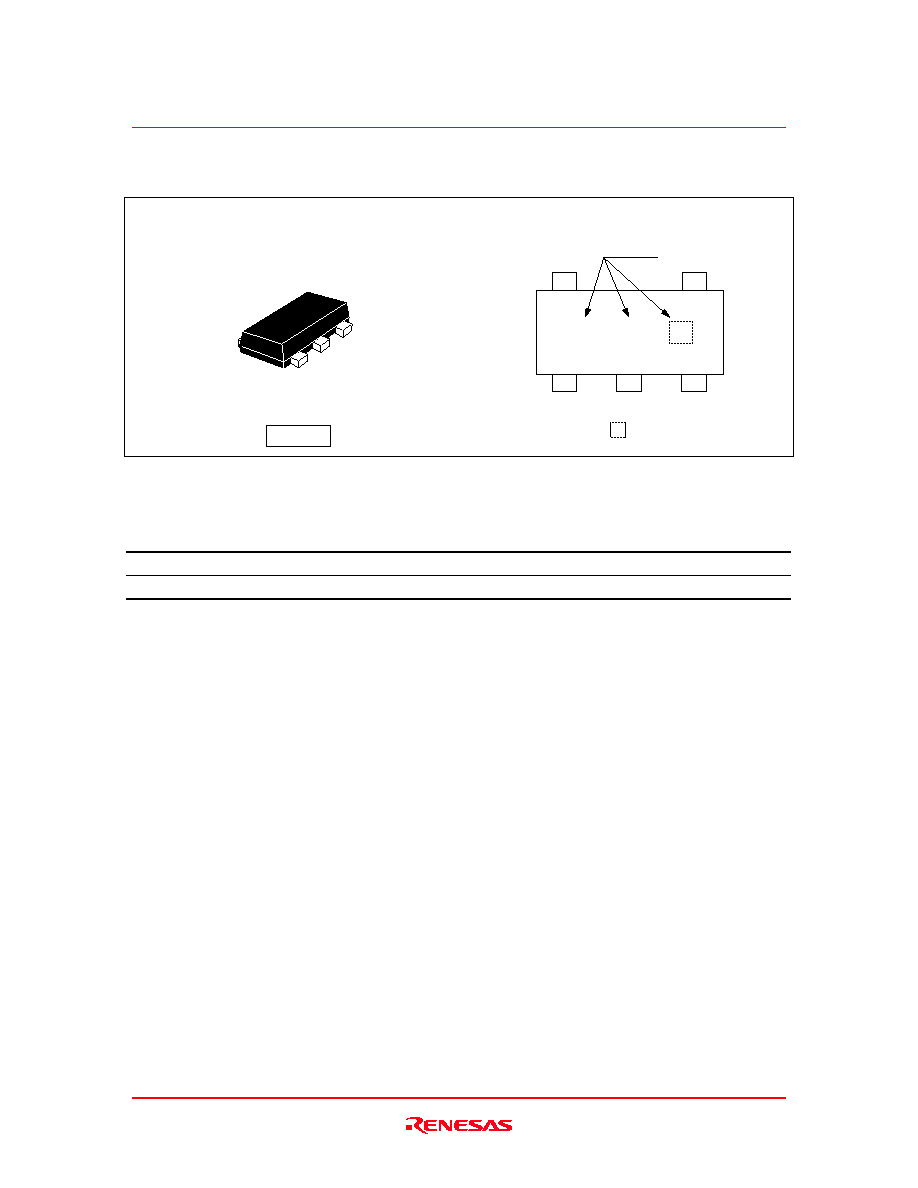
Outline and Article Indication
∑
HD74ALVC1G14
Marking
= Control code
A A
VSON-5
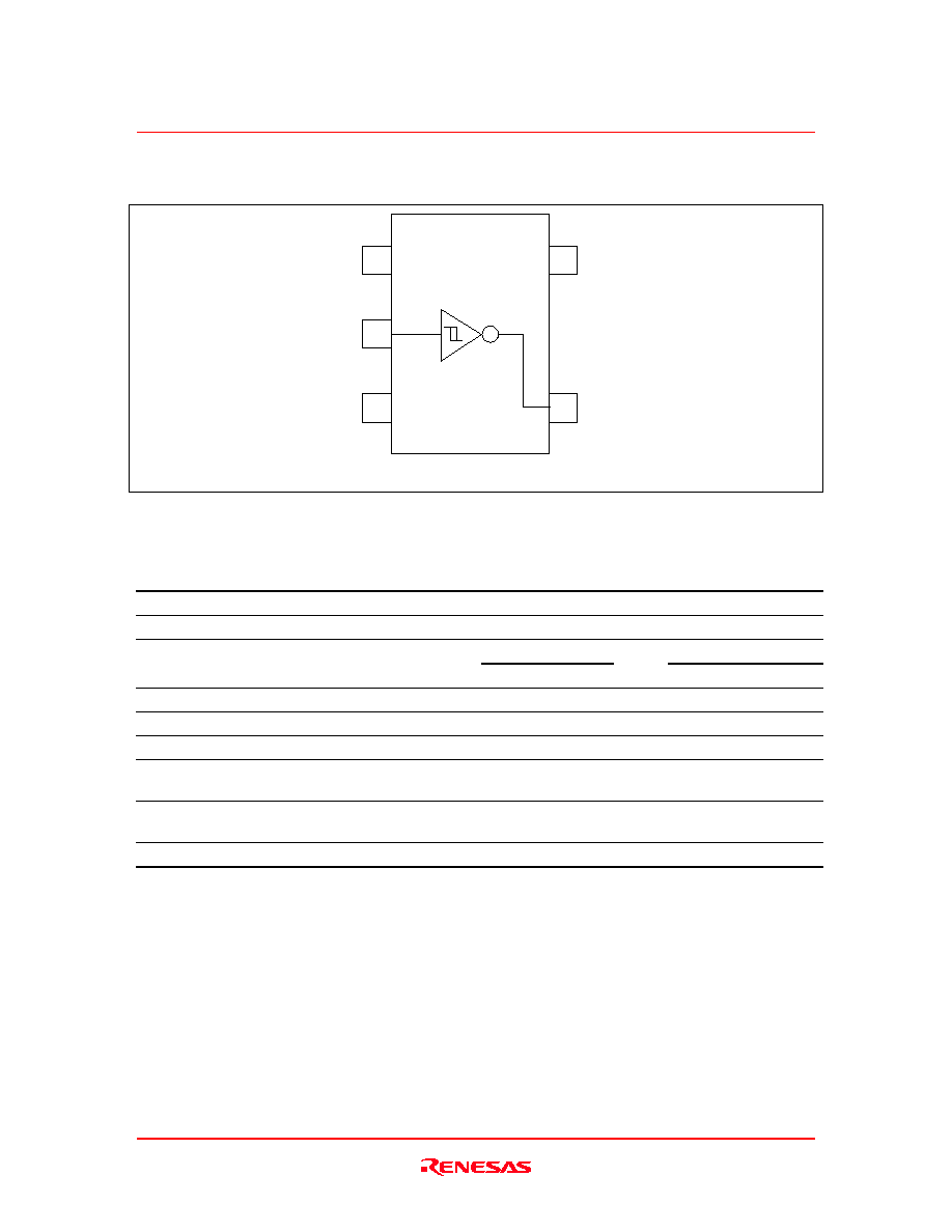
Function Table
Input A
Output
Y
H
L
L
H
H:
High level
L:
Low level
HD74ALVC1G14
Rev.3.00, Nov.12.2003, page 3 of 9
Pin Arrangement
(Top view)
1
NC
IN A
GND
V
CC
OUT
Y
2
3
5
4
Absolute Maximum Ratings
Item
Symbol
Ratings
Unit
Conditions
Supply voltage range
V
CC
-
0.5 to 4.6
V
Input voltage range
*1
V
I
-
0.5 to 4.6
V
-
0.5 to V
CC
+0.5
Output : H or L
Output voltage range
*1, 2
V
O
-
0.5 to 4.6
V
V
CC
: OFF
Input clamp current
I
IK
-
50
mA
V
I
< 0
Output clamp current
I
OK
±
50
mA
V
O
< 0 or V
O
> V
CC
Continuous output current
I
O
±
50
mA
V
O
= 0 to V
CC
Continuous current through
V
CC
or GND
I
CC
or I
GND
±
100
mA
Maximum power dissipation
at Ta = 25∞C (in still air)
*3
P
T
200
mW
Storage temperature
Tstg
-
65 to 150
∞C
Notes:
The absolute maximum ratings are values, which must not individually be exceeded, and
furthermore, no two of which may be realized at the same time.
1. The input and output voltage ratings may be exceeded if the input and output clamp-current
ratings are observed.
2. This value is limited to 4.6 V maximum.
3. The maximum package power dissipation was calculated using a junction temperature of 150∞C.
HD74ALVC1G14
Rev.3.00, Nov.12.2003, page 4 of 9
Recommended Operating Conditions
Item
Symbol
Min
Max
Unit
Conditions
Supply voltage range
V
CC
1.2
3.6
V
Input voltage range
V
I
0
3.6
V
Output voltage range
V
O
0
V
CC
V
-
2
V
CC
= 1.2 V
-
4
V
CC
= 1.4 V
-
6
V
CC
= 1.65 V
-
18
V
CC
= 2.3 V
I
OH
-
24
V
CC
= 3.0 V
2
V
CC
= 1.2 V
4
V
CC
= 1.4 V
6
V
CC
= 1.65 V
18
V
CC
= 2.3 V
Output current
I
OL
24
mA
V
CC
= 3.0 V
Operating free-air temperature
Ta
-
40
85
∞C
Note: Unused or floating inputs must be held high or low.

HD74ALVC1G14
Rev.3.00, Nov.12.2003, page 5 of 9
Electrical Characteristics
(Ta =
-
40 to 85∞C)
Item
Symbol V
CC
(V)
*
Min
Typ
Max
Unit
Test conditions
1.2
V
CC
◊
0.8
1.4 to 1.6
V
CC
◊
0.75
1.65 to 1.95
V
CC
◊
0.7
2.3 to 2.7
1.7
V
T
+
3.0 to 3.6
2.0
V
1.2
V
CC
◊
0.2
1.4 to 1.6
V
CC
◊
0.25
1.65 to 1.95 V
CC
◊
0.3
2.3 to 2.7
0.7
V
T
-
3.0 to 3.6
0.8
1.2
0.1
0.4
1.4 to 1.6
0.1
0.6
1.65 to 1.95 0.15
0.8
2.3 to 2.7
0.25
1.0
Threshold voltage
V
T
3.0 to 3.6
0.25
1.2
Min to Max
V
CC
-
0.2
I
OH
=
-
100
µ
A
1.2
0.9
I
OH
=
-
2 mA
1.4
1.1
I
OH
=
-
4 mA
1.65
1.2
I
OH
=
-
6 mA
2.3
1.7
I
OH
=
-
18 mA
V
OH
3.0
2.2
I
OH
=
-
24 mA
Min to Max
0.2
I
OL
= 100
µ
A
1.2
0.3
I
OL
= 2 mA
1.4
0.3
I
OL
= 4 mA
1.65
0.3
I
OL
= 6 mA
2.3
0.55
I
OL
= 18 mA
Output voltage
V
OL
3.0
0.55
V
I
OL
= 24 mA
Input current
I
IN
3.6
±
5
µ
A
V
IN
= 3.6 V or GND
Quiescent supply
current
I
CC
3.6
10
µ
A
V
IN
= V
CC
or GND,
I
O
= 0
Output leakage
current
I
OFF
0
5
µ
A
V
IN
or V
OUT
=
0 to 3.6 V
Input capacitance
C
IN
3.3
4.5
pF
V
IN
= V
CC
or GND
Note: For conditions shown as Min or Max, use the appropriate values under recommended operating
conditions.