Document Outline
- ˛ˇ
- ˛ˇ
- ˛ˇ
- ˛ˇ
- ˛ˇ
- ˛ˇ
- ˛ˇ
- ˛ˇ
- ˛ˇ
- ˛ˇ

Regarding the change of names mentioned in the document, such as Mitsubishi
Electric and Mitsubishi XX, to Renesas Technology Corp.
The semiconductor operations of Hitachi and Mitsubishi Electric were transferred to Renesas
Technology Corporation on April 1st 2003. These operations include microcomputer, logic, analog
and discrete devices, and memory chips other than DRAMs (flash memory, SRAMs etc.)
Accordingly, although Mitsubishi Electric, Mitsubishi Electric Corporation, Mitsubishi
Semiconductors, and other Mitsubishi brand names are mentioned in the document, these names
have in fact all been changed to Renesas Technology Corp. Thank you for your understanding.
Except for our corporate trademark, logo and corporate statement, no changes whatsoever have been
made to the contents of the document, and these changes do not constitute any alteration to the
contents of the document itself.
Note : Mitsubishi Electric will continue the business operations of high frequency & optical devices
and power devices.
Renesas Technology Corp.
Customer Support Dept.
April 1, 2003
To all our customers

1
Mitsubishi microcomputers
M30221 Group
SINGLE-CHIP 16-BIT CMOS MICROCOMPUTER
Description
Description
The M30221 group of single-chip microcomputers are built using the high-performance silicon gate CMOS
process using a M16C/60 Series CPU core. The M30221 group has LCD controller/driver. M30221 group is
packaged in a 120-pin plastic molded QFP. These single-chip microcomputers operate using sophisticated
instructions featuring a high level of instruction efficiency. With 1M bytes of address space, they are ca-
pable of executing instructions at high speed.
Features
∑ Basic machine instructions .................. Compatible with the M16C/60 series
∑ Memory capacity .................................. See Figure 1.1.3 Memory Expansion
∑ Shortest instruction execution time ...... 100ns (f(X
IN
)=10MHz)
∑ Supply voltage ..................................... 4.0 to 5.5V (f(X
IN
)=10MHz)
2.7 to 5.5V (f(X
IN
)=7MHz with software one-wait)
∑ Interrupts .............................................. 24 internal and 8 external interrupt sources, 4 software
interrupt sources; 7 levels(including key input interrupt)
∑ Multifunction 16-bit timer ...................... Timer A (output) x 8, timer B (input) x 6
∑ Real time port outputs .......................... 8 bits X 3 lines,6 bits X 1 lines
∑ Serial I/O .............................................. 2 channels for UART or clock synchronous
∑ DMAC .................................................. 2 channels (trigger: 24 souces)
∑ A-D converter ....................................... 10 bits X 7 channels
∑ D-A converter ....................................... 8 bits X 2 channels
∑ Watchdog timer .................................... 1 line
∑ Programmable I/O ............................... 83 lines (26 lines are shared with LCD outputs)
∑ Output port ........................................... 14 lines (14 lines are shared with LCD outpus)
∑ Input port .............................................. 1 line (P7
7
, shared with NMI pin)
∑ LCD drive control circuit ....................... 1/2, 1/3 bias
2, 3 and 4 duty
4 common outputs
40 segment outputs
built-in charge pump
∑ Key input interrupt ................................ 20 lines
∑ Clock generating circuit ....................... 2 built-in clock generation circuits
(built-in feedback resistor, and external ceramic or quartz oscillator)
Applications
Camera, Home appliances, Portable equipment, Audio, office equipment, etc.
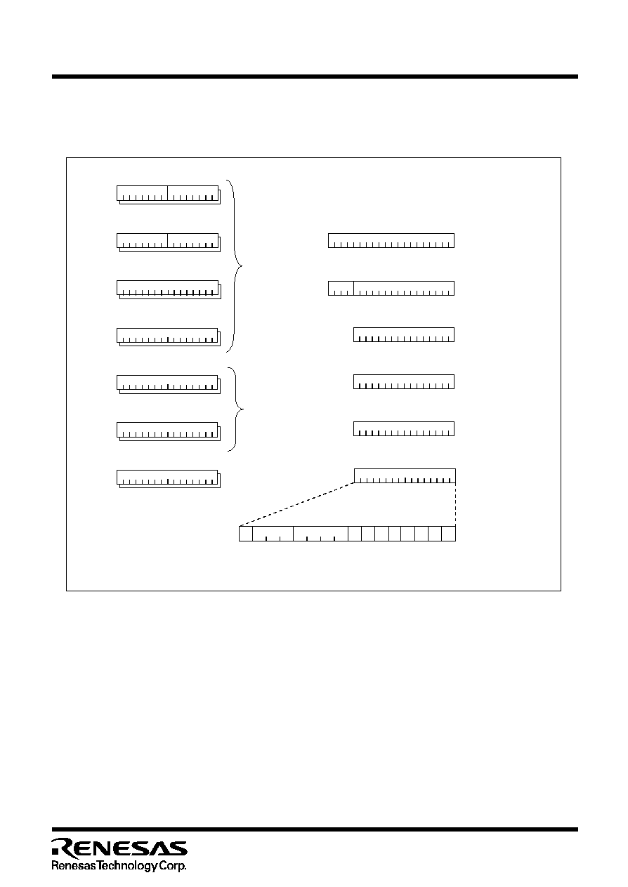
------Table of Contents------
Central Processing Unit (CPU) ................................ 9
Reset ...................................................................... 12
Programmable I/O Port .......................................... 18
Electric Characteristics .......................................... 28
Usage precaution peculiar to M30221 Group ........ 41
Specifications written in this manual
are believed to be accurate, but are
not guaranteed to be entirely free of
error.
Specifications in this manual may
be changed for functional or
performance improvements. Please
make sure your manual is the latest
edition.
2
Mitsubishi microcomputers
M30221 Group
SINGLE-CHIP 16-BIT CMOS MICROCOMPUTER
Description
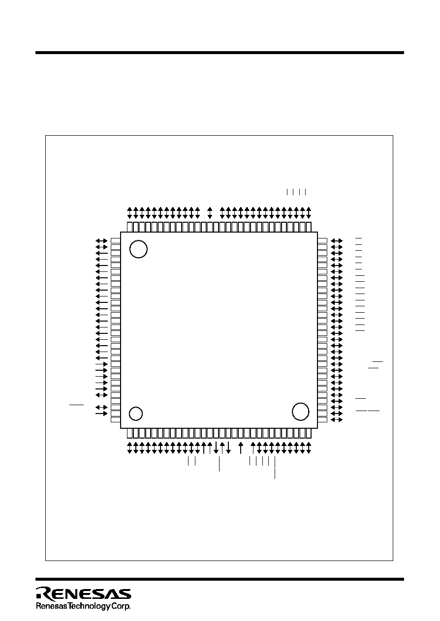
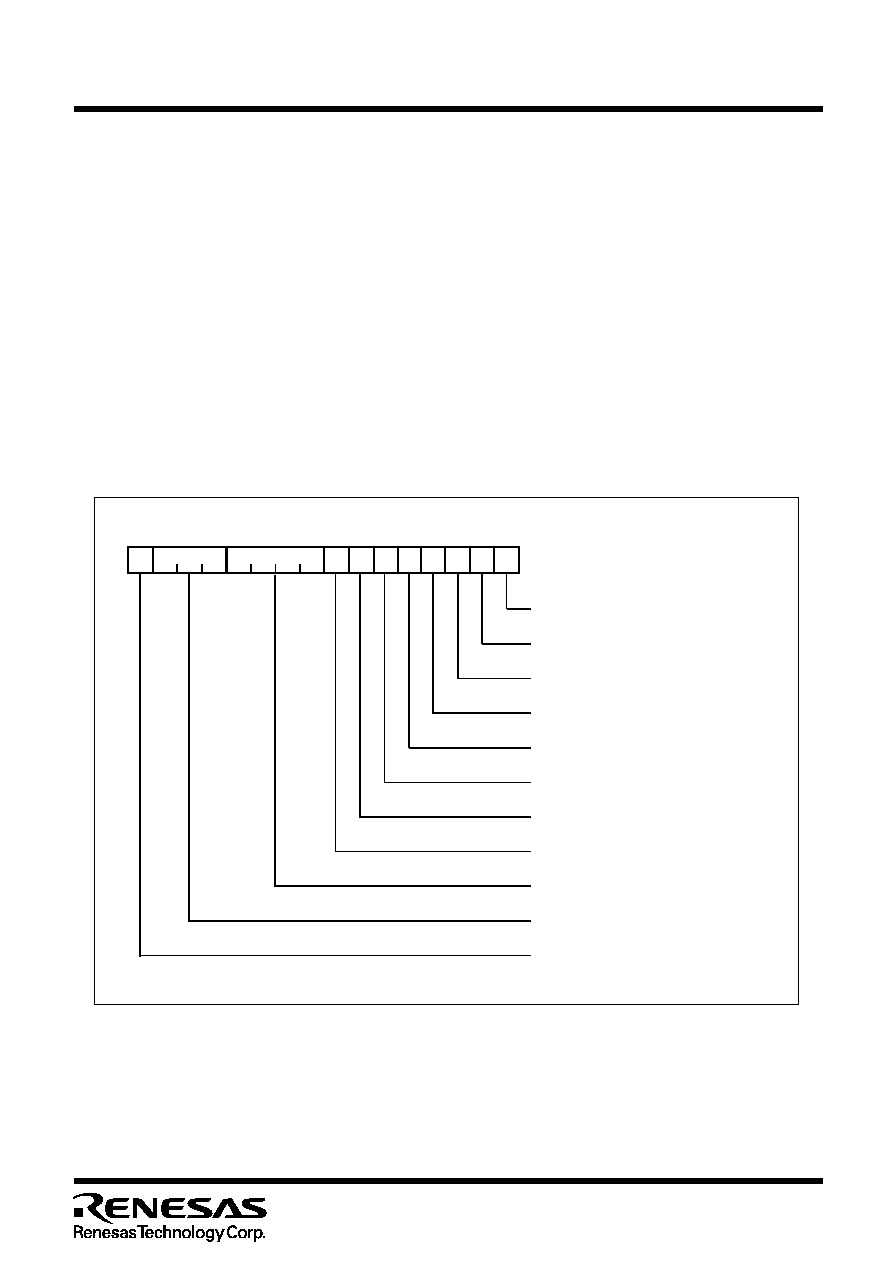
Pin Configuration
Figures 1.1.1 show the pin configurations (top view).
PIN CONFIGURATION (top view)
Package: 120P6R-A
Figure 1.1.1. Pin configuration for the M30221 group (top view)
92
95
120
119
118
117
116
115
114
113
112
111
110
108
107
106
105
104
103
102
101
100
99
98
97
96
91
93
94
109
59
56
31
32
33
34
35
36
37
38
39
40
41
43
44
45
46
47
48
49
50
51
52
53
54
55
60
58
57
42
AV
CC
SEG
10
SEG
9
SEG
7
SEG
6
SEG
5
SEG
4
SEG
3
SEG
8
SEG
15
SEG
14
SEG
12
SEG
11
SEG
13
SEG
2
C
1
V
L3
V
L2
V
L1
C
2
COM
3
COM
2
COM
1
COM
0
AV
SS
V
REF
P13
1
/DA
1
P13
0
/AD
TRG
/DA
0
2
5
30
29
28
27
26
25
24
23
22
21
20
18
17
16
15
14
13
12
11
10
9
8
7
6
1
3
4
19
89
86
61
62
63
64
65
66
67
68
69
70
71
73
74
75
76
77
78
79
80
81
82
83
84
85
90
88
87
72
P9
3
/AN
3
P9
2
/AN
2
P9
1
/AN
1
P9
4
/AN
4
P9
5
/AN
5
P9
6
/AN
6
P9
0
/AN
0
P8
6
/TA7
OUT
P8
4
/TA6
OUT
P7
1
/R
X
D
2
/SCL(Note)
X
OUT
V
SS
X
IN
V
CC
X
COUT
X
CIN
CNV
SS
P8
2
/TA5
OUT
P7
0
/T
X
D
2
/SDA(Note)
P7
2
/CLK
2
P6
3
/TxD
0
P6
2
/RxD
0
P8
1
/TA4
IN
/INT
5
P8
0
/TA4
OUT
/INT
5
RESET
P7
7
/NMI
P7
6
/INT
2
P7
5
/INT
1
P7
4
/INT
0
P7
3
/CTS
2
/RTS
2
P5
7
/CK
OUT
P5
3
/TB3
IN
P4
2
/TA1
OUT
P4
1
/TA0
IN
P6
1
/CLK
0
P5
0
/TB0
IN
P5
1
/TB1
IN
P5
2
/TB2
IN
P3
5
P3
4
P6
0
/CTS
0
/RTS
0
P5
6
/INT3
P4
7
/TA3
IN
/INT4
P4
6
/TA3
OUT
/INT4
P3
3
/KI
19
P3
2
/KI
18
P3
1
/KI
17
P3
0
/KI
16
P2
7
/KI
15
P2
6
/KI
14
P2
5
/KI
13
P2
4
/KI
12
P2
3
/KI
11
P2
2
/KI
10
P2
1
/KI
9
P2
0
/KI
8
P1
7
/KI
7
P1
6
/KI
6
P1
5
/KI
5
P1
4
/KI
4
P12
1
/SEG
3
3
P12
0
/SEG
3
2
P11
6
/SEG
3
0
P11
5
/SEG
2
9
P11
4
/SEG
2
8
V
CC
V
SS
P12
5
/SEG
3
7
P12
3
/SEG
35
P12
2
/SEG
34
P12
4
/SEG
36
P0
0
/SEG
40
P0
1
/SEG
41
P0
2
/SEG
42
P0
3
/SEG
43
P0
4
/SEG
44
P0
5
/SEG
45
P0
6
/SEG
46
P0
7
/SEG
47
P11
3
/SEG
27
P11
1
/SEG
25
P11
0
/SEG
24
P10
3
/SEG
19
P10
2
/SEG
18
P11
2
/SEG
26
P11
7
/SEG
3
1
P1
0
/KI
0
P1
1
/KI
1
P1
2
/KI
2
P1
3
/KI
3
P10
0
/SEG
16
P10
1
/SEG
17
M30221MX-XXXFP
Note. N channel open-drain output.
3
Mitsubishi microcomputers
M30221 Group
SINGLE-CHIP 16-BIT CMOS MICROCOMPUTER
Description
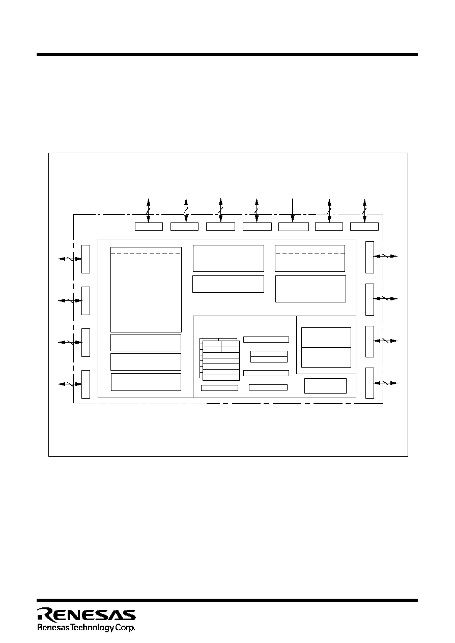
Block Diagram
Figure 1.1.2 is a block diagram of the M30221 group.
Figure 1.1.2. Block diagram of M30221 group
Timer
Internal peripheral functions
Watchdog timer
(15 bits)
Memory
ROM
(Note 1)
RAM
(Note 2)
A-D converter
(10 bits
X
7 channels
UART/clock synchronous SI/O
(8 bits
X
2 channels)
System clock generator
X
IN
-X
OUT
X
CIN
-X
COUT
M16C/60 series 16-bit CPU core
I/O ports
Port P4
4
Port P5
6
Port P6
4
Port P7
7
Port P7
7
1
Port P8
5
R0L
R0H
R1H
R1
L
R
2
R
3
A
0
A
1
FB
R0L
R0H
R1H
R1L
R2
R3
A0
A1
FB
Registers
SB
ISP
USP
Stack pointer
Multiplier
Vector table
INTB
Port P9
7
Flag register
FLG
Program counter
PC
Note 1: ROM size depends on MCU type.
Note 2: RAM size depends on MCU type.
DMAC
(2 channels)
D-A converter
(8 bits X 2 channels)
LCD drive control circuit
(4COM X 40SEG)
Port P10
4
Port P12
6
Port P13
2
Port P3
6
Port P2
8
Port P1
8
Port P0
8
Port P11
8
Timer TA0 (16 bits)
Timer TA1 (16 bits)
Timer TA2 (16 bits)
Timer TA3 (16 bits)
Timer TA4 (16 bits)
Timer TA5 (16 bits)
Timer TA6 (16 bits)
Timer TA7 (16 bits)
Timer TB0 (16 bits)
Timer TB1 (16 bits)
Timer TB2 (16 bits)
Timer TB3 (16 bits)
Timer TB4 (16 bits)
Timer TB5 (16 bits)
4
Mitsubishi microcomputers
M30221 Group
SINGLE-CHIP 16-BIT CMOS MICROCOMPUTER
Description
Item
Performance
Number of basic instructions
91 instructions
Shortest instruction execution time
100ns (f(X
IN
)=10MHz
Memory
ROM
24 Kbytes
capacity
RAM
1.5 Kbytes
I/O port
P0 to P13 (except P7
7
)
8 bits x 4, 2 bits x 1, 6 bits x 3, 7 bits x 2
5 bits x 1, 4 bits x 3
Input port
P7
7
1 bit x 1
Output port
SEG2 to SEG15
2 bits x 7
Multifunction
TA0 to TA7
16 bits x 8
timer
TB0 to TB5
16 bits x 6
Real time port outputs
8 bits x 3 lines,6 bits x 1 lines
Serial I/O
UART0 , UART2
(UART or clock synchronous) x 2
A-D converter
10 bits x 7 channels
D-A converter
8 bits x 2 channels
DMAC
2 channel(trigger:24 sources)
LCD
COM0 to COM3
4 lines
SEG2 to SEG47
40 lines (26 lines are shared with I/O ports)
Watchdog timer
15 bits x 1 (with prescaler)
Interrupt
24 internal and 8 external sources, 4 software sources
Clock generating circuit
2 built-in clock generation circuits
(built-in feedbackresistor, and external ceramic or
quartz oscillator)
Supply voltage
4.0 to 5.5V (f(X
IN
)=10MHz)
2.7 to 5.5V (f(X
IN
)=7MHz with software one-wait)
Power consumption
18 mW (Vcc=3.3V, f(X
IN
)=7MHz with software one-wait)
I/O withstand voltage (P0 to P13)
5 V
Output current P1 to P9,P13
5 mA
P0, P10 to P12
0.1mA("H" output), 2.5mA("L" output)
Device configuration
CMOS silicon gate
Package
120-pin plastic mold QFP
Table 1.1.1. Performance outline of M30221 group
Performance Outline
Table 1.1.1 is performance outline of M30221 group.
I/O char-
acteristics

5
Mitsubishi microcomputers
M30221 Group
SINGLE-CHIP 16-BIT CMOS MICROCOMPUTER
Description
Mitsubishi plans to release the following products in the M30221 group:
(1) Support for mask ROM version, flash memory version
(2) Memory capacity
(3) Package
120P6R-A
: Plastic molded QFP (mask ROM and flash memory versions)
Figure 1.1.3 shows the memory expansion and figure 1.1.4 shows the Type No., memory size, and pack-
age.
Figure 1.1.3. Memory expansion
Figure 1.1.4. Type No., memory size, and package
April. 2001
Type No. M30 22 1 M 3 - XXX FP
Package type:
FP:
Package120P6R-A
ROM capacity:
3 : 24K bytes
8 : 64K bytes
4 : 32K bytes
C : 128K bytes
ROM No.
Omitted for flash memory version
Memory type:
M : Mask ROM version
F : Flash memory version
Shows pin count, etc.
(The value itself has no specific meaning)
M16C/22 Group(built-in LCDC)
M16C Family
Shows characteristic, use
None: General
2K
RAM
Byte
32K
ROM
Byte
128K
10K
M30221FCFP
Under development
4K
64K
M30221M8-XXXFP
M30221MC-XXXFP
Under planning
Under planning
M30221M3-XXXFP
M30221M4-XXXFP
Under planning
24K
1.5K
6
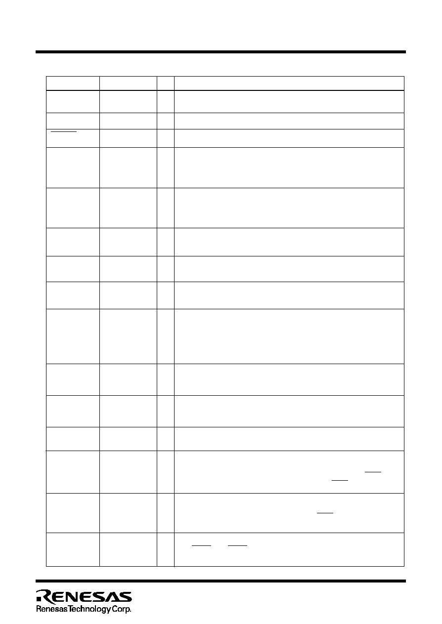
Pin Description
Mitsubishi microcomputers
M30221 Group
SINGLE-CHIP 16-BIT CMOS MICROCOMPUTER
Pin Description
V
CC
, V
SS
CNV
SS
X
IN
X
OUT
AV
CC
AV
SS
V
REF
P0
0
to P0
7
P1
0
to P1
7
P3
0
to P3
5
P4
1,
P4
2,
P4
6,
P4
7
Signal name
Power supply
input
CNV
SS
Reset input
Clock input
Clock output
Analog power
supply input
Reference
voltage input
I/O port P0
I/O port P1
I/O port P3
I/O port P4
Supply 2.7 to 5.5 V to the V
CC
pin. Supply 0 V to the V
SS
pin.
Function
Connect it to the V
SS
pin.
A "L" on this input resets the microcomputer.
This pin is a reference voltage input for the A-D converter.
Pin name
I/O
Analog power
supply input
RESET
I/O port P5
I/O port P6
P5
0
to P5
3,
P5
6,
P5
7
P6
0
to P6
3
P2
0
to P2
7
I/O port P2
I
I
I
O
I
I/O
I/O
I/O
I/O
I/O
I/O
I/O
X
CIN
X
COUT
Clock input
Clock output
I
O
These pins are provided for the sub clock generating
circuit.Connect a ceramic resonator or crystal between the X
CIN
and the X
COUT
pins. To use an externally derived clock, input it
to the X
CIN
pin and leave the X
COUT
open.
These pins are provided for the main clock generating.
circuit.Connect a ceramic resonator or crystal between the X
IN
and the X
OUT
pins. To use an externally derived clock, input it
to the X
IN
pin and leave the X
OUT
open.
This pin is a power supply input for the A-D converter. Connect
it to VCC.
This pin is a power supply input for the A-D converter. Connect
it to VSS.
This is an 8-bit CMOS I/O port. It has an input/output port
direction register that allows the user to set each pin for input or
output individually. When set for input, the user can specify in
units of four bits via software whether or not they are tied to a
pull-up resistor. Pins in this port also use as LCD segment
output and real time port output.
This is an 8-bit I/O port equivalent to P0. Pins in this port also
function as input pins for the key input interrupt function and real
time port output.
This is an 8-bit I/O port equivalent to P0. Pins in this port also
function as input pins for the key input interrupt function and real
time port output.
This is a 6-bit I/O port equivalent to P0. P3
0
to P3
3
also function
as input pins for the key input interrupt function.
This is a 4-bit I/O port equivalent to P0. The P4
1
pin is shared
with timer A0 input. The P4
2
pin is shared with timer A1
output. The P4
6
pin is shared with timer A3 output and INT4.
The P4
7
pin is shared with timer A3 input and INT4.
This is a 6-bit I/O port equivalent to P0. The P5
0
, P5
1
, P5
2
, and
P5
3
pins are shared with timerB0, B1, B2, and B3 input,
respectively. The P5
6
pin is shared with INT3. The P5
7
pin is
shared with CKOUT output.
This is an 4-bit I/O port equivalent to P0. The P60 pin is shared
with CTS
0
and RTS
0
. The P6
1
, P6
2
, and P6
3
pins are shared
with CLK
0
, RxD
0
, and TxD
0
, respectively.

7
Pin Description
Mitsubishi microcomputers
M30221 Group
SINGLE-CHIP 16-BIT CMOS MICROCOMPUTER
Pin Description
Signal name
Function
Pin name
I/O
I/O
I/O
I/O
I/O port P7
I/O port P8
I/O port P9
I/O port P10
P7
0
to P7
6
P8
0
to P8
2
,
P8
4
,
P8
6
P9
0
to P9
6
P10
0
to P10
3
This is an 7-bit I/O port equivalent to P0. Pins in this port also
function as A-D converter input pins.
This is an 4-bit I/O port equivalent to P0. Pins in this port also
function as SEG output for LCD.
P7
7
I
This is an 2-bit I/O port equivalent to P0. P13
0
pins in this port
also function as D-A converter output pins or start trigger for A-D
input pins. P13
1
pins in this port also function as D-A converter
output pins.
I/O
I/O port P11
P11
0
to P11
7
This is an 8-bit I/O port equivalent to P0. Pins in this port also
function as SEG output for LCD.
I/O
I/O port P13
P13
0
, P13
1
O
Segment output
SEG
2
to
SEG
15
Pins in this port function as SEG output for LCD drive circuit.
O
Common
output
COM
0
to
COM
3
Power supply input for LCD drive circuit.
Power supply
input for LCD
V
L1
to V
L3
Pins in this port function as common output for LCD drive circuit.
Step-up
condenser
connect port
C
1
, C
2
Pins in this port function as external pin for LCD step-up
condenser. Connect a condenser between C
1
and C
2
.
I/O
I/O port P12
P12
0
to P12
5
This is an 6-bit I/O port equivalent to P0. Pins in this port also
function as SEG output for LCD and real time port output.
P7
0
to P7
6
are I/O ports equivalent to P0 (P7
0
and P7
1
are N
channel open-drain output).
The P7
0
, P7
1
, and P7
2
pins are shared with TxD
2
, RxD
2
, and
CLK
2
, respectively. The P7
3
is shared with CTS
2
and RTS
2
. The
P7
4
, P7
5
and P7
6
pins are shared with INT
0
, INT
1
and INT
2
,
respectively.
P7
7
is an input-only port that also functions for NMI.
This is a 5-bit I/O port equivalent to P0. The P8
0
pin is shared
with timer A4 output and INT5 input . The P8
1
pin is shared with
timer A4 input and INT5 input. The P8
2
pin is shared with timer
A5 output. The P8
4
pin is shared with timer A6 output. The P8
6
pin is shared with timer A7 output.
I/O

8
Memory
Mitsubishi microcomputers
M30221 Group
SINGLE-CHIP 16-BIT CMOS MICROCOMPUTER
Operation of Functional Blocks
The M30221 group accommodates certain units in a single chip. These units include ROM and RAM to
store instructions and data and the central processing unit (CPU) to execute arithmetic/logic operations.
Also included are peripheral units such as timers, real time port, serial I/O, LCD drive control circuit, D-A
converter, A-D converter, DMAC and I/O ports.
Memory
Figure 1.4.1 is a memory map of the M30221 group. The address space extends the 1M bytes from ad-
dress 00000
16
to FFFFF
16
. From FFFFF
16
down is ROM. For example, in the M30221M3-XXXFP, there is
24K bytes of internal ROM from FA000
16
to FFFFF
16
. The vector table for fixed interrupts such as the reset
_______
and NMI are mapped to FFFDC
16
to FFFFF
16
. The starting address of the interrupt routine is stored here.
The address of the vector table for timer interrupts, etc., can be set as desired using the internal register
(INTB). See the section on interrupts for details.
From 00400
16
up is RAM. For example, in the M30221M3-XXXFP, 1.5K bytes of internal RAM is mapped
to the space from 00400
16
to 009FF
6
. In addition to storing data, the RAM also stores the stack used when
calling subroutines and when interrupts are generated.
The SFR area is mapped to 00000
16
to 003FF
16
. This area accommodates the control registers for periph-
eral devices such as I/O ports, A-D converter, serial I/O, timers, and LCD, etc. Figures 1.7.1 to 1.7.3 are
location of peripheral unit control registers. Any part of the SFR area that is not occupied is reserved and
cannot be used for other purposes.
The special page vector table is mapped to FFE00
16
to FFFDB
16
. If the starting addresses of subroutines
or the destination addresses of jumps are stored here, subroutine call instructions and jump instructions
can be used as 2-byte instructions, reducing the number of program steps.
Figure 1.4.1. Memory map
SFR area
For details, see
Figures 1.7.1 to 1.7.3
Internal RAM area
Internal RAM area
Internal ROM area
Reset
Watchdog timer
Single step
Address match
BRK instruction
Overflow
Undefined instruction
Special page
vector table
00000
16
00400
16
XXXXX
16
YYYYY
16
FFFFF
16
FFFFF
16
FFFDC
16
FFE00
16
DBC
NMI
ROM size
FA000
16
24K bytes
Address YYYYY
16
32K bytes
64K bytes
128K bytes
F8000
16
F0000
16
E0000
16
RAM size
009FF
16
1.5K bytes
Address XXXXX
16
2K bytes
4K bytes
10K bytes
00BFF
16
013FF
16
02BFF
16
9
CPU
Mitsubishi microcomputers
M30221 Group
SINGLE-CHIP 16-BIT CMOS MICROCOMPUTER
Central Processing Unit (CPU)
The CPU has a total of 13 registers shown in Figure 1.5.1. Seven of these registers (R0, R1, R2, R3, A0,
A1, and FB) come in two sets; therefore, these have two register banks.
(1) Data registers (R0, R0H, R0L, R1, R1H, R1L, R2, and R3)
Data registers (R0, R1, R2, and R3) are configured with 16 bits, and are used primarily for transfer and
arithmetic/logic operations.
Registers R0 and R1 each can be used as separate 8-bit data registers, high-order bits as (R0H/R1H),
and low-order bits as (R0L/R1L). In some instructions, registers R2 and R0, as well as R3 and R1 can
use as 32-bit data registers (R2R0/R3R1).
(2) Address registers (A0 and A1)
Address registers (A0 and A1) are configured with 16 bits, and have functions equivalent to those of data
registers. These registers can also be used for address register indirect addressing and address register
relative addressing.
In some instructions, registers A1 and A0 can be combined for use as a 32-bit address register (A1A0).
H
L
b15
b8
b7
b0
R0
(Note)
H
L
b15
b8
b7
b0
R1
(Note)
R2
(Note)
b15
b0
R3
(Note)
b15
b0
A0
(Note)
b15
b0
A1
(Note)
b15
b0
FB
(Note)
b15
b0
Data
registers
Address
registers
Frame base
registers
b15
b0
b15
b0
b15
b0
b15
b0
b0
b19
b0
b19
H
L
Program counter
Interrupt table
register
User stack pointer
Interrupt stack
pointer
Static base
register
Flag register
PC
INTB
USP
ISP
SB
FLG
Note: These registers consist of two register banks.
C
D
Z
S
B
O
I
U
IPL
Figure 1.5.1. Central processing unit register

10
CPU
Mitsubishi microcomputers
M30221 Group
SINGLE-CHIP 16-BIT CMOS MICROCOMPUTER
(3) Frame base register (FB)
Frame base register (FB) is configured with 16 bits, and is used for FB relative addressing.
(4) Program counter (PC)
Program counter (PC) is configured with 20 bits, indicating the address of an instruction to be executed.
(5) Interrupt table register (INTB)
Interrupt table register (INTB) is configured with 20 bits, indicating the start address of an interrupt vector
table.
(6) Stack pointer (USP/ISP)
Stack pointer comes in two types: user stack pointer (USP) and interrupt stack pointer (ISP), each config-
ured with 16 bits.
Your desired type of stack pointer (USP or ISP) can be selected by a stack pointer select flag (U flag).
This flag is located at the position of bit 7 in the flag register (FLG).
(7) Static base register (SB)
Static base register (SB) is configured with 16 bits, and is used for SB relative addressing.
(8) Flag register (FLG)
Flag register (FLG) is configured with 11 bits, each bit is used as a flag. Figure 1.5.2 shows the flag
register (FLG). The following explains the function of each flag:
∑ Bit 0: Carry flag (C flag)
This flag retains a carry, borrow, or shift-out bit that has occurred in the arithmetic/logic unit.
∑ Bit 1: Debug flag (D flag)
This flag enables a single-step interrupt.
When this flag is "1", a single-step interrupt is generated after instruction execution. This flag is
cleared to "0" when the interrupt is acknowledged.
∑ Bit 2: Zero flag (Z flag)
This flag is set to "1" when an arithmetic operation resulted in 0; otherwise, cleared to "0".
∑ Bit 3: Sign flag (S flag)
This flag is set to "1" when an arithmetic operation resulted in a negative value; otherwise, cleared to "0".
∑ Bit 4: Register bank select flag (B flag)
This flag chooses a register bank. Register bank 0 is selected when this flag is "0" ; register bank 1 is
selected when this flag is "1".
∑ Bit 5: Overflow flag (O flag)
This flag is set to "1" when an arithmetic operation resulted in overflow; otherwise, cleared to "0".
∑ Bit 6: Interrupt enable flag (I flag)
This flag enables a maskable interrupt.
An interrupt is disabled when this flag is "0", and is enabled when this flag is "1". This flag is cleared to
"0" when the interrupt is acknowledged.
11
CPU
Mitsubishi microcomputers
M30221 Group
SINGLE-CHIP 16-BIT CMOS MICROCOMPUTER
∑ Bit 7: Stack pointer select flag (U flag)
Interrupt stack pointer (ISP) is selected when this flag is "0" ; user stack pointer (USP) is selected
when this flag is "1".
This flag is cleared to "0" when a hardware interrupt is acknowledged or an INT instruction of software
interrupt Nos. 0 to 31 is executed.
∑ Bits 8 to 11: Reserved area
∑ Bits 12 to 14: Processor interrupt priority level (IPL)
Processor interrupt priority level (IPL) is configured with three bits, for specification of up to eight
processor interrupt priority levels from level 0 to level 7.
If a requested interrupt has priority greater than the processor interrupt priority level (IPL), the interrupt
is enabled.
∑ Bit 15: Reserved area
The C, Z, S, and O flags are changed when instructions are executed. See the software manual for
details.
Figure 1.5.2. Flag register (FLG)
Carry flag
Debug flag
Zero flag
Sign flag
Register bank select flag
Overflow flag
Interrupt enable flag
Stack pointer select flag
Reserved area
Processor interrupt priority level
Reserved area
Flag register (FLG)
C
D
Z
S
B
O
I
U
IPL
b0
b15
12
Reset
Mitsubishi microcomputers
M30221 Group
SINGLE-CHIP 16-BIT CMOS MICROCOMPUTER
____________
Table 1.6.1 shows the statuses of the other pins while the RESET pin level is "L". Figures 1.6.3 and 1.6.4
show the internal status of the microcomputer immediately after the reset is cancelled.
____________
Table 1.6.1. Pin status when RESET pin level is "L"
Status
Pin name
SEG
2
to SEG
15
P0, P10 to P12
Input port(with a pull up resistor)
Input port (floating)
"H" level is output
"H" level is output
COM
0
to COM
3
P1 to P9, P13
Figure 1.6.2. Reset sequence
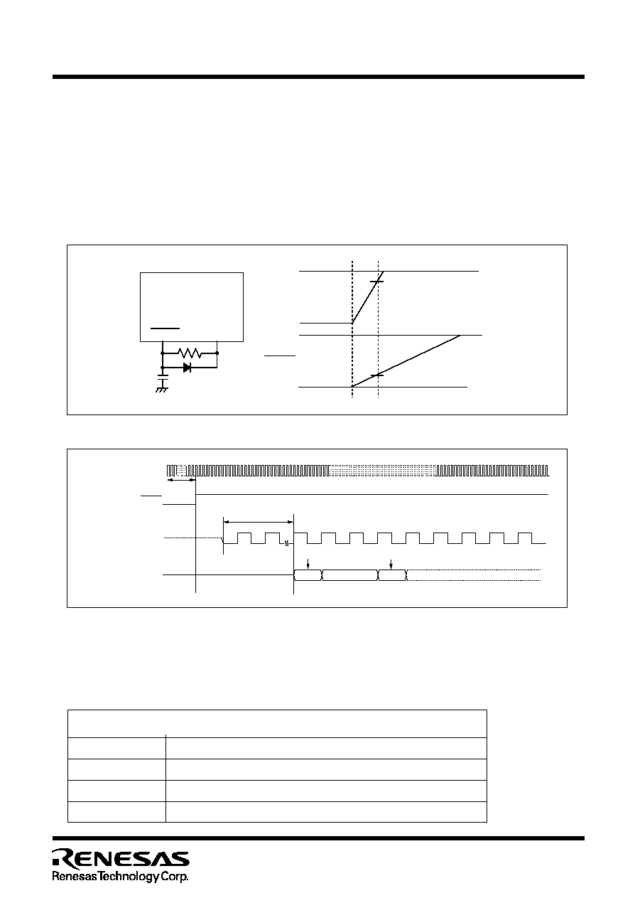
Reset
There are two kinds of resets; hardware and software. In both cases, operation is the same after the reset.
(See "Software Reset" for details of software resets.) This section explains on hardware resets.
When the supply voltage is in the range where operation is guaranteed, a reset is effected by holding the
reset pin level "L" (0.2V
CC
max.) for at least 20 cycles. When the reset pin level is then returned to the "H"
level while main clock is stable, the reset status is cancelled and program execution resumes from the
address in the reset vector table.
Figure 1.6.1 shows the example reset circuit. Figure 1.6.2 shows the reset sequence.
Figure 1.6.1. Example reset circuit
X
IN
Address
(Internal Address signal)
FFFFE
16
FFFFC
16
More than 20 cycles are needed
BCLK
BCLK 24 cycles
RESET
Content of reset vector
RESET
V
CC
0.8V
RESET
V
CC
0V
0V
5V
5V
4.0V
13
Reset
Mitsubishi microcomputers
M30221 Group
SINGLE-CHIP 16-BIT CMOS MICROCOMPUTER
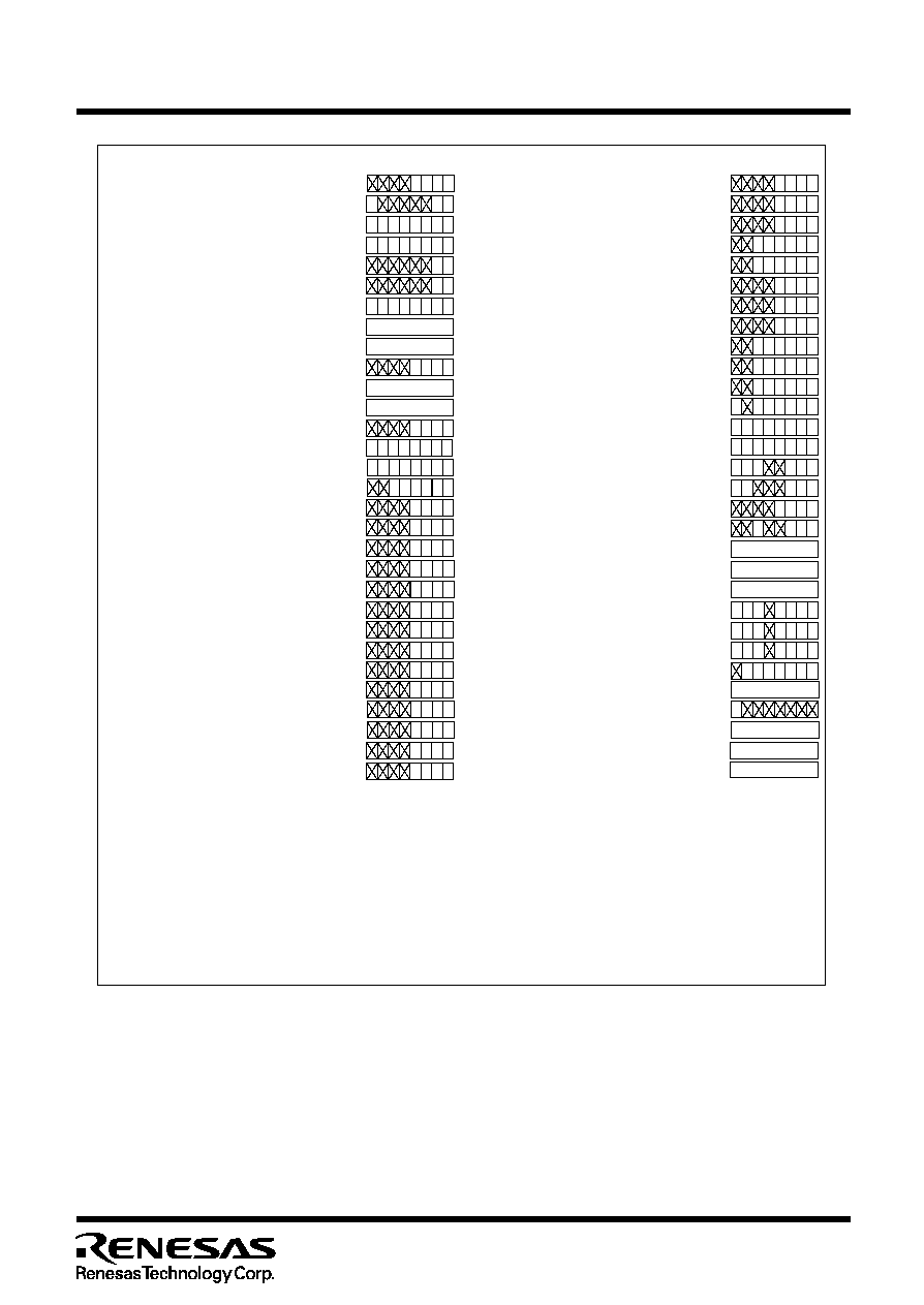
Figure 1.6.3. Device's internal status after a reset is cleared(1)
The content of other registers and RAM is undefined when the microcomputer is
reset. The initial values must therefore be set.
0 1 0 0 1 0 0 0
0 0
0
0 0
0
0
0
0
1
0 0 0 ? ? ? ? ?
00
16
00
16
0 0
0
0
00
16
00
16
0 0
0
0
0 0 0
?
0 0 0
?
0 0 0
?
0 0 0
?
0 0 0
?
0 0 0
?
0 0 0
?
0 0 0
?
0 0 0
?
0 0 0
?
0 0 ?
0 0
0
0 0 0
?
0 0 0
?
0 0
? 0 0
0
0
0
0 0
? 0 0
0
0
0
0
0
0
0
0
0
0
0 0
0 0 0
?
0 0 0
?
0 0 0
?
0 0 0
?
0 0 0
?
0 0
0 0 0
?
0 0
0 0 0
?
0 0
0 0 0
?
? 0 0 0
? 0 0 0
? 0 0 0
0 0 0 0
0
0 0 0
00
16
00
16
00
16
? 0 0 0
0
0
? 0 0 0
0
0
0
0
0
0 0 0
0
0
0
0
0 0 0
0
0 0 0
0 0 0
0 0
0 0 0
?
0 0 0
0 0
0
?
0 0 0
0 0
0
?
0 0 0
0 0
0
0
0 0 0
0
00
16
00
16
(26)UART0 receive interrupt control register
(0052
16
)∑∑∑
(1)Processor mode register 0
(0004
16
)∑∑∑
(2)Processor mode register 1
(0005
16
)∑∑∑
(3)System clock control register 0
(0006
16
)∑∑∑
(4)System clock control register 1
(0007
16
)∑∑∑
(5)Address match interrupt enable register
(0009
16
)∑∑∑
(6)Protect register
(000A
16
)∑∑∑
(7)Watchdog timer control register
(000F
16
)∑∑∑
(8)Address match interrupt register 0
(0010
16
)∑∑∑
(0011
16
)∑∑∑
(0012
16
)∑∑∑
(9)Address match interrupt register 1
(0014
16
)∑∑∑
(0015
16
)∑∑∑
(0016
16
)∑∑∑
(10)DMA0 control register
(002C
16
)∑∑∑
(11)DMA1 control register
(003C
16
)∑∑∑
(12)INT3 interrupt control register
(0044
16
)∑∑∑
(13)Timer B5 interrupt control register
(0045
16
)∑∑∑
(14)Timer B4 interrupt control register
(0046
16
)∑∑∑
(15)Timer B3 interrupt control register
(0047
16
)∑∑∑
(16)Timer A7 interrupt control register
(0048
16
)∑∑∑
(17)Timer A6 interrupt control register
(0049
16
)∑∑∑
(18)Timer A5 interrupt control register
(004A
16
)∑∑∑
(19)DMA0 interrupt control register
(004B
16
)∑∑∑
(20)DMA1 interrupt control register
(004C
16
)∑∑∑
(21)Key input interrupt control register
(004D
16
)∑∑∑
(22)A-D conversion interrupt control register
(004E
16
)∑∑∑
(23)UART2 transmit interrupt control register
(004F
16
)∑∑∑
(24)UART2 receive interrupt control register
(0050
16
)∑∑∑
(25)UART0 transmit interrupt control register
(0051
16
)∑∑∑
(56)UART2 transmit/receive mode register
(0378
16
)∑∑∑
(27)Timer A0 interrupt control register
(0055
16
)∑∑∑
(28)Timer A1 interrupt control register
(0056
16
)∑∑∑
(29)Timer A2 interrupt control register
(0057
16
)∑∑∑
(30)Timer A3 interrupt control register
(0058
16
)∑∑∑
(31)Timer A4 interrupt control register
(0059
16
)∑∑∑
(32)Timer B0 interrupt control register
(005A
16
)∑∑∑
(33)Timer B1 interrupt control register
(005B
16
)∑∑∑
(34)Timer B2 interrupt control register
(005C
16
)∑∑∑
(35)INT0 interrupt control register
(005D
16
)∑∑∑
(36)INT1 interrupt control register
(005E
16
)∑∑∑
(37)INT2 interrupt control register
(005F
16
)∑∑∑
(38)LCD mode register
(0120
16
)∑∑∑
(39)Segment output enable register
(0122
16
)∑∑∑
(40)Key input mode register
(0126
16
)∑∑∑
(41)Count start flag 1
(0340
16
)∑∑∑
(42)One-shot start flag 1
(0342
16
)∑∑∑
(43)Trigger select flag 1
(0343
16
)∑∑∑
(44)Up-down flag 1
(0344
16
)∑∑∑
(45)Timer A5 mode register
(0356
16
)∑∑∑
(46)Timer A6 mode register
(0357
16
)∑∑∑
(47)Timer A7 mode register
(0358
16
)∑∑∑
(48)Timer B3 mode register
(035B
16
)∑∑∑
(49)Timer B4 mode register
(035C
16
)∑∑∑
(50)Timer B5 mode register
(035D
16
)∑∑∑
(51)Interrupt cause select register 0
(035E
16
)∑∑∑
(52)Interrupt cause select register 1
(035F
16
)∑∑∑
(55)UART2 special mode register
(0377
16
)∑∑∑
0 1 1
0 0 0
0 0
(53)Clock division counter control register
(0360
16
)∑∑∑
0
00
16
(54)UART2 special mode register 2
(0376
16
)∑∑∑
x : Nothing is mapped to this bit
? : Undefined
00
16
0
0
0
14
Reset
Mitsubishi microcomputers
M30221 Group
SINGLE-CHIP 16-BIT CMOS MICROCOMPUTER
Figure 1.6.4. Device's internal status after a reset is cleared(2)
0 0 0 ? ? ?
00
16
00
16
00
16
00
16
00
16
00
16
00
16
00
16
00
16
00
16
00
16
0
0
0
0
0
0
0
0
0
0
0
0
0
00
16
(83)Port P0 direction register
(84)Port P1 direction register
(85)Port P2 direction register
(86)Port P3 direction register
(87)Port P4 direction register
(88)Port P5 direction register
(89)Port P6 direction register
(90)Port P7 direction register
(91)Port P8 direction register
(92)Port P9 direction register
(93)Port P10 direction register
(94)Port P11 direction register
0000
16
0000
16
0000
16
00000
16
0000
16
0000
16
0000
16
0000
16
00
16
0
0
0
00
16
(108)Flag register (FLG)
(95)Port P12 direction register
(96)Port P13 direction register
(97)Pull-up control register 0
(98)Pull-up control register 1
(99)Pull-up control register 2
(100)Real time port control register
(101)Data registers (R0/R1/R2/R3)
(102)Address registers (A0/A1)
(103)Frame base register (FB)
(104)Interrupt table register (INTB)
(105)User stack pointer (USP)
(106)Interrupt stack pointer (ISP)
(107)Static base register (SB)
00
16
1
1
0
0 0 0 0 0
0
0
0
1 1 1 1 0
(03E2
16
)∑ ∑ ∑
(03E3
16
)∑ ∑ ∑
(03E6
16
)∑ ∑ ∑
(03E7
16
)∑ ∑ ∑
(03EA
16
)∑ ∑ ∑
(03EB
16
)∑ ∑ ∑
(03EE
16
)∑ ∑ ∑
(03EF
16
)∑ ∑ ∑
(03F2
16
)∑ ∑ ∑
(03F3
16
)∑ ∑ ∑
(03F6
16
)∑ ∑ ∑
(03F7
16
)∑ ∑ ∑
(03FA
16
)∑ ∑ ∑
(03FB
16
)∑ ∑ ∑
(03FC
16
)∑ ∑ ∑
(03FD
16
)∑ ∑ ∑
(03FE
16
)∑ ∑ ∑
(03FF
16
)∑ ∑ ∑
∑ ∑ ∑
∑ ∑ ∑
∑ ∑ ∑
∑ ∑ ∑
∑ ∑ ∑
∑ ∑ ∑
∑ ∑ ∑
∑ ∑ ∑
(57)
UART2 transmit/receive control register 0
(58)
UART2 transmit/receive control register 1
(59)Count start flag 0
(60) Clock prescaler reset flag
(61)One-shot start flag 0
(62)Trigger select flag 0
(63)Up-down flag 0
(64)Timer A0 mode register
(65)Timer A1 mode register
(66)Timer A2 mode register
(82) D-A control register
(67)Timer A3 mode register
(68)Timer A4 mode register
(69)Timer B0 mode register
(70)Timer B1 mode register
(71)Timer B2 mode register
(72)
UART0 transmit/receive mode register
(73)
UART0 transmit/receive control register 0
(74)
UART0 transmit/receive control register 1
(75)
UART transmit/receive control register 2
(76)Flash memory control register
(Note)
(77)DMA0 cause select register
(78)DMA1 cause select register
(80)A-D control register 0
(81)A-D control register 1
(79)A-D control register 2
(037C
16
)∑ ∑ ∑
(037D
16
)∑ ∑ ∑
(0380
16
)∑ ∑ ∑
(0381
16
)∑ ∑ ∑
(0382
16
)∑ ∑ ∑
(0383
16
)∑ ∑ ∑
(0384
16
)∑ ∑ ∑
(0396
16
)∑ ∑ ∑
(0397
16
)∑ ∑ ∑
(0398
16
)∑ ∑ ∑
(0399
16
)∑ ∑ ∑
(039A
16
)∑ ∑ ∑
(039B
16
)∑ ∑ ∑
(039C
16
)∑ ∑ ∑
(039D
16
)∑ ∑ ∑
(03A0
16
)∑ ∑ ∑
(03A4
16
)∑ ∑ ∑
(03A5
16
)∑ ∑ ∑
(03B0
16
)∑ ∑ ∑
(03B4
16
)∑ ∑ ∑
(03B8
16
)∑ ∑ ∑
(03BA
16
)∑ ∑ ∑
(03D4
16
)∑ ∑ ∑
(03D6
16
)∑ ∑ ∑
(03D7
16
)∑ ∑ ∑
(03DC
16
)∑ ∑ ∑
00
16
0
0
0
0 0 0 0 1
0
1
0
0 0 0 0 0
00
16
00
16
00
16
00
16
00
16
00
16
00
16
00
16
00
16
x : Nothing is mapped to this bit
? : Undefined
0
0 0
0 0 0 0 0
0
?
0
0 0 0 0
0
?
0
0 0 0 0
0
?
0
0 0 0 0
0 0
0 1 0 0 0
0
0 0
0 0 0 1 0
0
0
0
0 0 0
0
The content of other registers and RAM is undefined when the microcomputer is reset. The initial values
must therefore be set.
Note : This register is only exist in flash memory version.
0
0 0 0 0 0
0
0
1
0
0
15
SFR
Mitsubishi microcomputers
M30221 Group
SINGLE-CHIP 16-BIT CMOS MICROCOMPUTER
Figure 1.7.1. Location of peripheral unit control registers (1)
0000
16
0001
16
0002
16
0003
16
0004
16
0005
16
0006
16
0007
16
0008
16
0009
16
000A
16
000B
16
000C
16
000D
16
000E
16
000F
16
0010
16
0011
16
0012
16
0013
16
0014
16
0015
16
0016
16
0017
16
0018
16
0019
16
001A
16
001B
16
001C
16
001D
16
001E
16
001F
16
0020
16
0021
16
0022
16
0023
16
0024
16
0025
16
0026
16
0027
16
0028
16
0029
16
002A
16
002B
16
002C
16
002D
16
002E
16
002F
16
0030
16
0031
16
0032
16
0033
16
0034
16
0035
16
0036
16
0037
16
0038
16
0039
16
003A
16
003B
16
003C
16
003D
16
003E
16
003F
16
0040
16
0041
16
0042
16
0043
16
0044
16
0045
16
0046
16
0047
16
0048
16
0049
16
004A
16
004B
16
004C
16
004D
16
004E
16
004F
16
0050
16
0051
16
0052
16
0053
16
0054
16
0055
16
0056
16
0057
16
0058
16
0059
16
005A
16
005B
16
005C
16
005D
16
005E
16
005F
16
0100
16
0101
16
0102
16
0103
16
0104
16
0105
16
0106
16
0107
16
0108
16
0109
16
010A
16
010B
16
010C
16
010D
16
010E
16
010F
16
0110
16
0111
16
0112
16
0113
16
0114
16
0115
16
0116
16
0117
16
0120
16
0121
16
0122
16
0123
16
0124
16
0125
16
0126
16
INT1 interrupt control register (INT1IC)
Timer B0 interrupt control register (TB0IC)
Timer B2 interrupt control register (TB2IC)
Timer A1 interrupt control register (TA1IC)
Timer A3 interrupt control register (TA3IC)
UART0 transmit interrupt control register (S0TIC)
INT2 interrupt control register (INT2IC)
INT0 interrupt control register (INT0IC)
Timer B1 interrupt control register (TB1IC)
Timer A0 interrupt control register (TA0IC)
Timer A2 interrupt control register (TA2IC)
Timer A4 interrupt control register (TA4IC)
UART0 receive interrupt control register (S0RIC)
UART1 transmit interrupt control register (S1TIC)
UART1 receive interrupt control register (S1RIC)
Key input interrupt control register (KUPIC)
A-D conversion interrupt control register (ADIC)
Watchdog timer start register (WDTS)
Watchdog timer control register (WDC)
Processor mode register 0 (PM0)
Address match interrupt register 0 (RMAD0)
Address match interrupt register 1 (RMAD1)
System clock control register 0 (CM0)
System clock control register 1 (CM1)
Address match interrupt enable register (AIER)
Protect register (PRCR)
Processor mode register 1(PM1)
INT3 interrupt control register (INT3IC)
INT4 interrupt control register (INT4IC)
INT5 interrupt control register (INT5IC)
Timer B5 interrupt control register (TB5IC)
Timer B4 interrupt control register (TB4IC)
Timer B3 interrupt control register (TB3IC)
UART2 transmit interrupt control register (S2TIC)
UART2 receive interrupt control register (S2RIC)
Timer A7 interrupt control register (TA7IC)
Timer A6 interrupt control register (TA6IC)
Timer A5 interrupt control register (TA5IC)
DMA0 source pointer (SAR0)
DMA0 destination pointer (DAR0)
DMA0 transfer counter (TCR0)
DMA0 control register (DM0CON)
DMA1 source pointer (SAR1)
DMA1 destination pointer (DAR1)
DMA1 transfer counter (TCR1)
DMA1 control register (DM1CON)
LCD RAM0(LRAM0)
LCD RAM1(LRAM1)
LCD RAM2(LRAM2)
LCD RAM3(LRAM3)
LCD RAM4(LRAM4)
LCD RAM5(LRAM5)
LCD RAM6(LRAM6)
LCD RAM7(LRAM7)
LCD RAM8(LRAM8)
LCD RAM9(LRAM9)
LCD RAM12(LRAM12)
LCD RAM13(LRAM13)
LCD RAM14(LRAM14)
LCD RAM15(LRAM15)
LCD RAM16(LRAM16)
LCD RAM17(LRAM17)
LCD RAM18(LRAM18)
LCD RAM20(LRAM20)
LCD RAM21(LRAM21)
LCD RAM22(LRAM22)
LCD RAM23(LRAM23)
DMA0 interrupt control register (DM0IC)
DMA1 interrupt control register (DM1IC)
LCD mode register (LCDM)
Segment output enable register (SEG)
Key input mode register (KUPM)
LCD frame frequency counter (LCDTIM)
Bus collision detection interrupt control register
(BCNIC)
Note : Locations in the SFR area where nothing is allocated are reserved areas. Do not access these areas for
read or write.
16
SFR
Mitsubishi microcomputers
M30221 Group
SINGLE-CHIP 16-BIT CMOS MICROCOMPUTER
Figure 1.7.2. Location of peripheral unit control registers (2)
0340
16
0341
16
0342
16
0343
16
0344
16
0345
16
0346
16
0347
16
0348
16
0349
16
034A
16
034B
16
034C
16
034D
16
034E
16
034F
16
0350
16
0351
16
0352
16
0353
16
0354
16
0355
16
0356
16
0357
16
0358
16
0359
16
035A
16
035B
16
035C
16
035D
16
035E
16
035F
16
0360
16
0361
16
0362
16
0363
16
0364
16
0365
16
0366
16
0367
16
0368
16
0369
16
036A
16
036B
16
036C
16
036D
16
036E
16
036F
16
0370
16
0371
16
0372
16
0373
16
0374
16
0375
16
0376
16
0377
16
0378
16
0379
16
037A
16
037B
16
037C
16
037D
16
037E
16
037F
16
0380
16
0381
16
0382
16
0383
16
0384
16
0385
16
0386
16
0387
16
0388
16
0389
16
038A
16
038B
16
038C
16
038D
16
038E
16
038F
16
0390
16
0391
16
0392
16
0393
16
0394
16
0395
16
0396
16
0397
16
0398
16
0399
16
039A
16
039B
16
039C
16
039D
16
039E
16
039F
16
03A0
16
03A1
16
03A2
16
03A3
16
03A4
16
03A5
16
03A6
16
03A7
16
03A8
16
03A9
16
03AA
16
03AB
16
03AC
16
03AD
16
03AE
16
03AF
16
03B0
16
03B1
16
03B2
16
03B3
16
03B4
16
03B5
16
03B6
16
03B7
16
03B8
16
03B9
16
03BA
16
03BB
16
03BC
16
03BD
16
03BE
16
03BF
16
UART0 transmit/receive mode register (U0MR)
UART0 transmit buffer register (U0TB)
UART0 receive buffer register (U0RB)
Timer A0 register (TA0)
Timer A1 register (TA1)
Timer A2 register (TA2)
Timer B0 register (TB0)
Timer B1 register (TB1)
Timer B2 register (TB2)
Count start flag 0 (TABSR0)
One-shot start flag 0 (ONSF0)
Timer A0 mode register (TA0MR)
Timer A1 mode register (TA1MR)
Timer A2 mode register (TA2MR)
Timer B0 mode register (TB0MR)
Timer B1 mode register (TB1MR)
Timer B2 mode register (TB2MR)
Up-down flag 0 (UDF0)
Timer A3 register (TA3)
Timer A4 register (TA4)
Timer A3 mode register (TA3MR)
Timer A4 mode register (TA4MR)
Trigger select register 0 (TRGSR0)
UART0 bit rate generator (U0BRG)
UART0 transmit/receive control register 0 (U0C0)
UART0 transmit/receive control register 1 (U0C1)
UART transmit/receive control register 2 (UCON)
Clock prescaler reset flag (CPSRF)
Count start flag 1 (TABSR1)
Timer B3 register (TB3)
Timer B4 register (TB4)
Timer B5 register (TB5)
Timer B3 mode register (TB3MR)
Timer B4 mode register (TB4MR)
Timer B5 mode register(TB5MR)
Timer A5 register (TA5)
Timer A6 register (TA6)
Timer A7 register (TA7)
One-shot start flag 1 (ONSF1)
Trigger select register 1 (TRGSR1)
Up-down flag 1(UDF1)
Timer A5 mode register (TA5MR)
Timer A6 mode register (TA6MR)
Timer A7 mode register (TA7MR)
UART2 special mode register (U2SMR)
UART2 transmit/receive mode register (U2MR)
UART2 bit rate generator (U2BRG)
UART2 transmit buffer register (U2TB)
UART2 transmit/receive control register 0 (U2C0)
UART2 transmit/receive control register 1 (U2C1)
UART2 receive buffer register (U2RB)
Interrupt cause select register 1 (IFSR1)
DMA0 request cause select register (DM0SL)
DMA1 request cause select register (DM1SL)
Clock division counter (CDC)
Interrupt cause select register 0 (IFSR0)
Clock division counter control register (CDCC)
UART2 special mode register 2(U2SMR2)
Flash memory control register (FMCR)(Note)
Note1 : This register is only exist in flash memory version.
Note2 : Locations in the SFR area where nothing is allocated are reserved areas. Do not access these areas for
read or write.

17
SFR
Mitsubishi microcomputers
M30221 Group
SINGLE-CHIP 16-BIT CMOS MICROCOMPUTER
Figure 1.7.3. Location of peripheral unit control registers (3)
03C0
16
03C1
16
03C2
16
03C3
16
03C4
16
03C5
16
03C6
16
03C7
16
03C8
16
03C9
16
03CA
16
03CB
16
03CC
16
03CD
16
03CE
16
03CF
16
03D0
16
03D1
16
03D2
16
03D3
16
03D4
16
03D5
16
03D6
16
03D7
16
03D8
16
03D9
16
03DA
16
03DB
16
03DC
16
03DD
16
03DE
16
03DF
16
03E0
16
03E1
16
03E2
16
03E3
16
03E4
16
03E5
16
03E6
16
03E7
16
03E8
16
03E9
16
03EA
16
03EB
16
03EC
16
03ED
16
03EE
16
03EF
16
03F0
16
03F1
16
03F2
16
03F3
16
03F4
16
03F5
16
03F6
16
03F7
16
03F8
16
03F9
16
03FA
16
03FB
16
03FC
16
03FD
16
03FE
16
03FF
16
Port P0 register (P0)
Port P0 direction register (PD0)
Port P1 register (P1)
Port P1 direction register (PD1)
Port P2 register (P2)
Port P2 direction register (PD2)
Port P3 register (P3)
Port P3 direction register (PD3)
Port P4 register (P4)
Port P4 direction register (PD4)
Port P5 register (P5)
Port P5 direction register (PD5)
Port P6 register (P6)
Port P6 direction register (PD6)
Port P7 register (P7)
Port P7 direction register (PD7)
Port P8 register (P8)
Port P8 direction register (PD8)
Port P9 register (P9)
Port P9 direction register (PD9)
Port P10 register (P10)
Port P10 direction register (PD10)
Pull-up control register 0 (PUR0)
Pull-up control register 1 (PUR1)
Pull-up control register 2 (PUR2)
A-D register 0 (AD0)
A-D register 1 (AD1)
A-D register 2 (AD2)
A-D register 3 (AD3)
A-D register 4 (AD4)
A-D register 5 (AD5)
A-D register 6 (AD6)
A-D control register 0 (ADCON0)
A-D control register 1 (ADCON1)
D-A register 0 (DA0)
D-A register 1 (DA1)
D-A control register (DACON)
A-D control register 2 (ADCON2)
Port P11 register (P11)
Port P11 direction register (PD11)
Port P12 register (P12)
Port P12 direction register (PD12)
Real time port control register (RTP)
Port P13 register (P13)
Port P13 direction register (PD13)
Note : Locations in the SFR area where nothing is allocated are reserved areas.
Do not access these areas for read or write.

18
Programmable I/O Port
Mitsubishi microcomputers
M30221 Group
SINGLE-CHIP 16-BIT CMOS MICROCOMPUTER
Programmable I/O Ports
There are 83 programmable I/O ports: P0 to P13 (excluding P7
7
). Each port can be set independently for
input or output using the direction register. A pull-up resistance for each block of 4 ports can be set. P7
7
is
an input-only port and has no built-in pull-up resistance.
Figures 1.19.1 to 1.19.4 show the programmable I/O ports. Figure 1.19.5 shows the I/O pins.
Each pin functions as a programmable I/O port and as the I/O for the built-in peripheral devices.
To use the pins as the inputs for the built-in peripheral devices, set the direction register of each pin to input
mode. When the pins are used as the outputs for the built-in peripheral devices (other than the D-A con-
verter), they function as outputs regardless of the contents of the direction registers. When pins are to be
used as the outputs for the D-A converter, do not set the direction registers to output mode.
(1) Direction registers
These registers are used to choose the direction of the programmable I/O ports. Each bit in these regis-
ters corresponds one for one to each I/O pin.
Note: There is no direction register bit for P7
7
.
(2) Port registers
These registers are used to write and read data for input and output to and from an external device. A
port register consists of a port latch to hold output data and a circuit to read the status of a pin. Each bit
in port registers corresponds one for one to each I/O pin.
(3) Pull-up control registers
The pull-up control register can be set to apply a pull-up resistance to each block of 4 ports. When ports
are set to have a pull-up resistance, the pull-up resistance is connected only when the direction register is
set for input. The pull-up resistance is not connected for pins that are set for output from peripheral
functions, regardless of the setting in the pull-up control register. When pull-up is ON for ports P1 and P2,
an intermittent pull-up that pulls up the port for only a set period of time, can be performed from the key
input mode register.
(4) Key input mode register
With bits 0 and 1 of this register, it is possible to select both edges or the fall edge of the key input for P1
and P2. Also, with bit 2, it is possible to make the pull-up for a port (P1 or P2), which is set for pull-up using
the pull-up control register, automatically connect as an intermittent pull-up. And, using the significant 3
bits, the pull-up resistance can be connected to and disconnected from ports P12 and P13.
(5) Real-time port control register
The real-time port control register can be used to set the registers of ports P0, P1, P2 and P12 for real-
time port output, whereby output is synchronized with timer overflow of timers A0, A1, A5 and A6 in the
timer mode.
19
Programmable I/O Port
Mitsubishi microcomputers
M30221 Group
SINGLE-CHIP 16-BIT CMOS MICROCOMPUTER
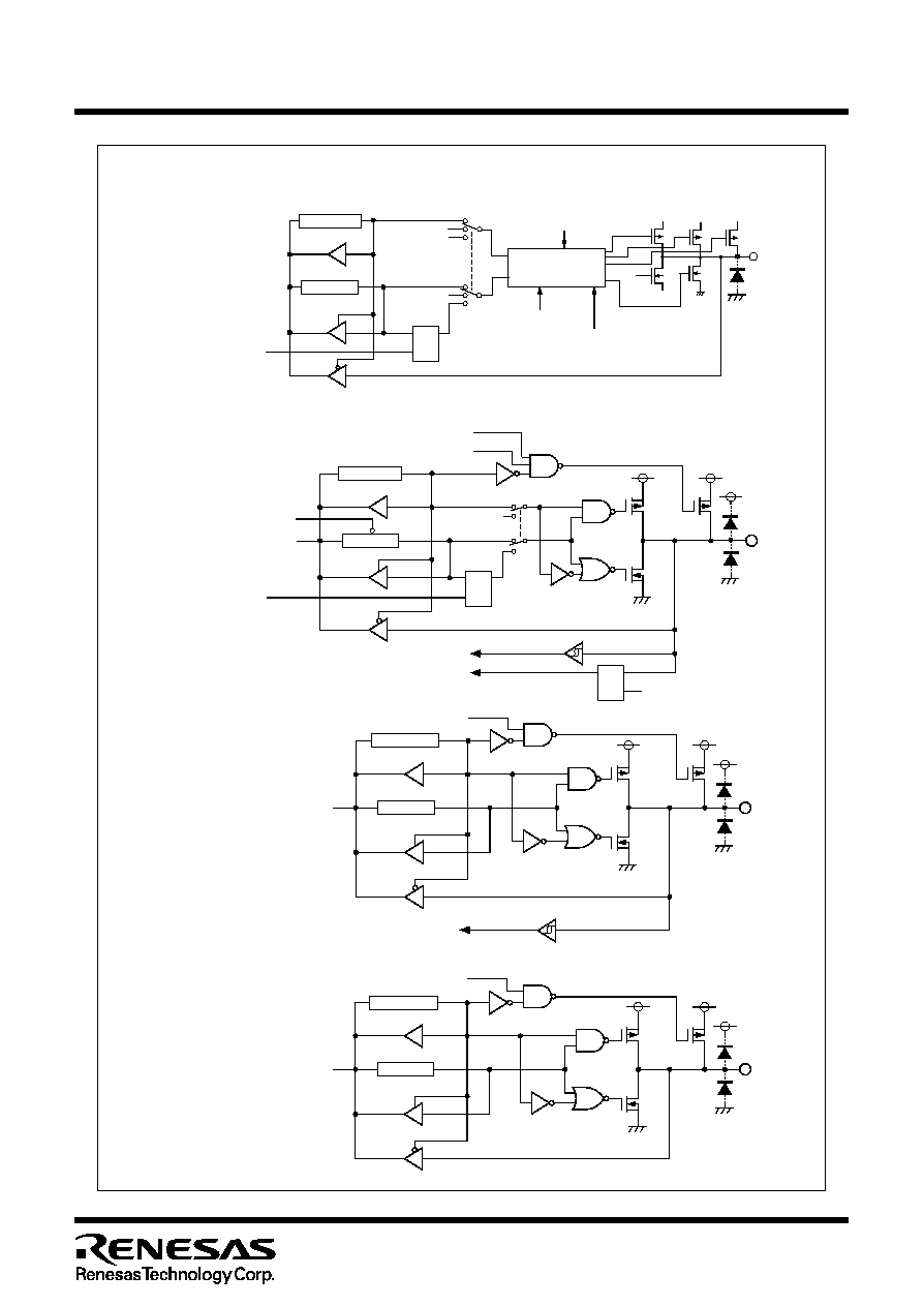
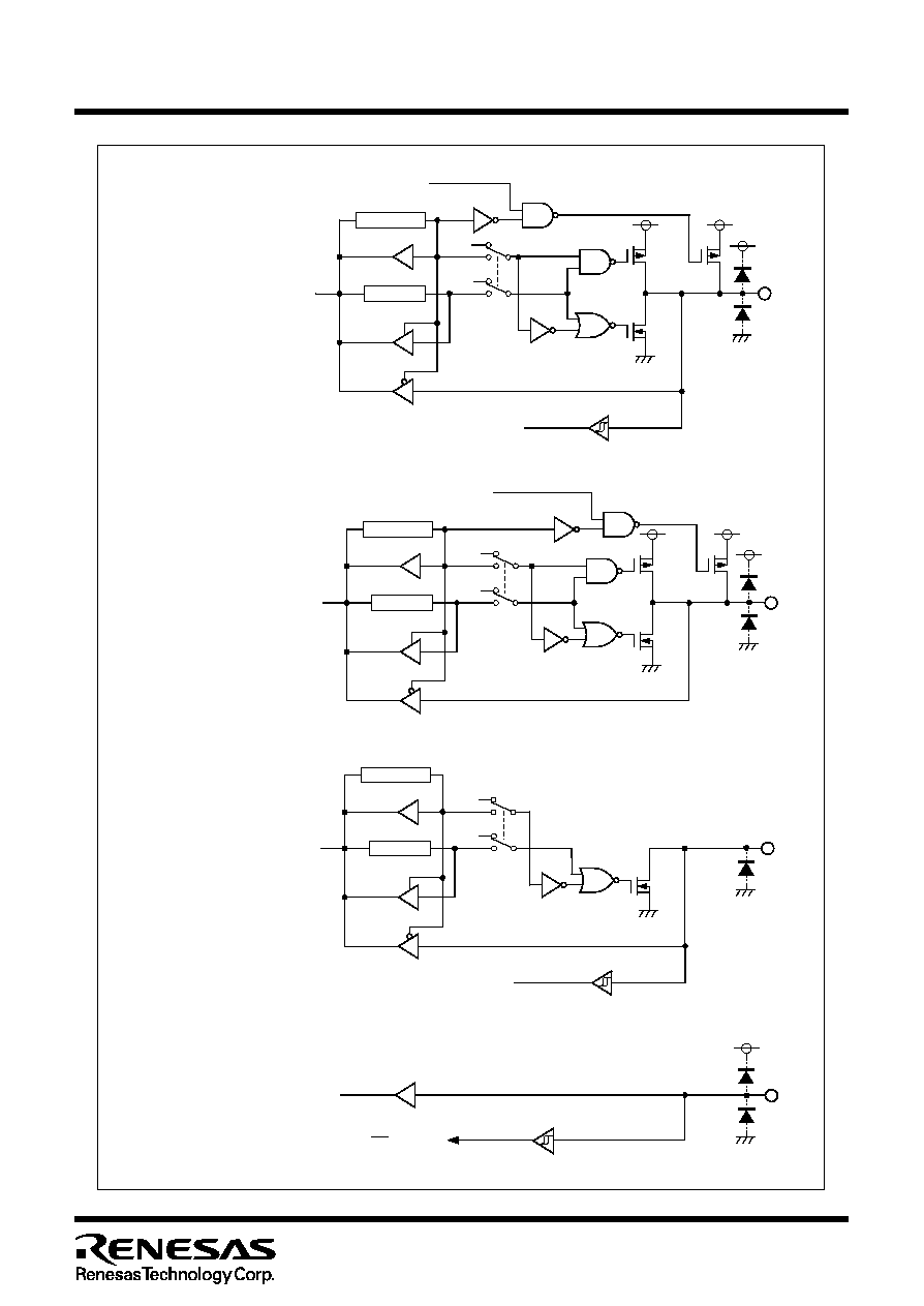
Figure 1.19.1. Programmable I/O ports (1)
P1
0
to P1
7
, P2
0
to P2
7
P0
0
to P0
7,
P12
0
to P12
5
Data bus
Direction register
Port latch
Pull-up selected
P3
0
to P3
3,
P4
1,
P4
7,
P5
0
to P5
3,
P5
6,
P6
2,
P7
4
to P7
6,
P8
1
Data bus
Direction register
Port latch
Pull-up selection
P3
4
, P3
5
Port ON/OFF
LCD drive timing
Port/segment
V
L1
/V
SS
V
L3
/V
CC
Data bus
Direction register
Port latch
Timer A
overflow
"1"
"1"
Segment output
D
CK
Q
V
L3
/V
CC
V
L2
/V
CC
Data bus
Direction register
Port latch
Pull-up selection
Timer A
overflow
Intermittent pull-up control
"1"
D
CK
Q
D
CK
Q
Interface logic
level shift circuit
Intermittent pull-up control
20
Programmable I/O Port
Mitsubishi microcomputers
M30221 Group
SINGLE-CHIP 16-BIT CMOS MICROCOMPUTER
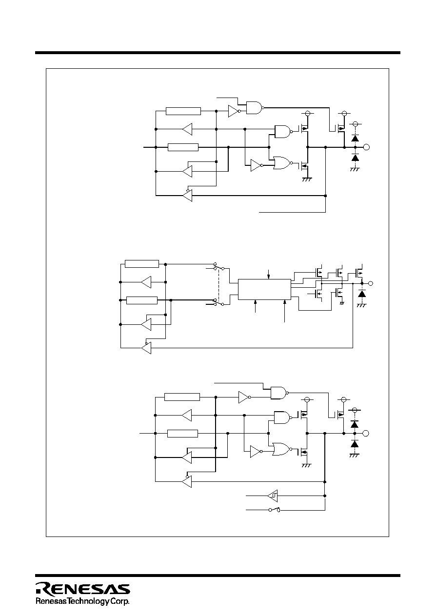
Figure 1.19.2. Programmable I/O ports (2)
P4
2
, P4
6
, P6
0
, P6
1
,
P7
2,
P7
3
, P8
0
, P8
2
,
P8
4
, P8
6
P5
7,
P6
3
Data bus
Direction register
Port latch
Pull-up selection
Output
Data bus
Direction register
Port latch
Pull-up selection
Output
P7
0,
P7
1
Data bus
Direction register
Port latch
Output
Input respective peripheral functions
P7
7
Data bus
NMI interrupt input
"1"
"1"
Input respective peripheral functions
"1"
21
Programmable I/O Port
Mitsubishi microcomputers
M30221 Group
SINGLE-CHIP 16-BIT CMOS MICROCOMPUTER
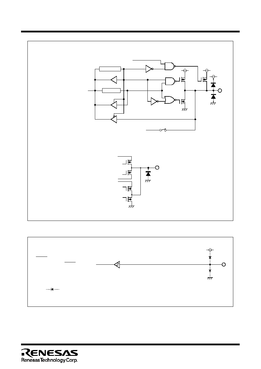
Figure 1.19.3. Programmable I/O ports (3)
P9
0 to
P9
6
Data bus
Direction register
Port latch
Pull-up selection
Analog input
P10
0
to P10
3,
P11
0
to P11
7
Port ON/OFF
LCD drive timing
Port/segment
Interface logic
level shift circuit
Data bus
Direction register
Port latch
"1"
Segment output
V
L1
/V
SS
V
L3
/V
CC
V
L3
/V
CC
V
L2
/V
CC
P13
0
Data bus
Direction register
Analog output
Pull-up selection
Input respective peripheral functions
Port latch
22
Programmable I/O Port
Mitsubishi microcomputers
M30221 Group
SINGLE-CHIP 16-BIT CMOS MICROCOMPUTER
Figure 1.19.5. I/O pins
Figure 1.19.4. Programmable I/O ports (4)
P13
1
Data bus
Direction register
Port latch
Analog output
Pull-up selection
COM
0
to COM
3
, SEG
2
to SEG
15
V
L3
V
L2
V
L1
V
SS
The gate input signal of each
transistor is controlled by the
LCD duty ratio and the bias
value.
Note :
symbolizes a parasitic diode.
Do not apply a voltage higher than V
CC
to each pin.
(Note)
RESET
RESET signal input
23
Programmable I/O Port
Mitsubishi microcomputers
M30221 Group
SINGLE-CHIP 16-BIT CMOS MICROCOMPUTER
Table 1.19.1. Example connection of unused pins in single-chip mode
Figure 1.19.13. Example connection of unused pins
Port P0 to P13 (except for P7
7
)
(Input mode)
∑
(Input mode)
(Output mode)
NMI
AV
CC
AV
SS
V
REF
Microcomputer
V
CC
V
SS
Open
∑
∑
∑
V
L3
V
L2
V
L1
CNV
SS
Open
Open
Open
X
COUT
COM
0
COM
3
SEG
2
SEG
15
X
CIN
Note 1: If setting these pins in output mode and opening them, ports are in input mode untill switched into
output mode by use of software after reset. Thus the voltage levels of the pins become unstable,
and there can be instances in which the power source current increases while the ports are in input
mode. In view of an instance in which the contents of the direction registers change due to a
runaway generated by noise or other causes, setting the contents of the direction registers
periodically by use of software increases program reliability.
Note 2: With external clock input to XIN pin.
Note 3: Output "L" if port P70 and P71 are set to output mode.Port P70 and P71 are N channel open drain.
Pin name
Connection
Ports P0 to P13
(excluding P7
7
)
X
OUT
(Note 2),X
COUT
AV
SS
, V
REF
AV
CC
After setting for output mode, leave these pins open; or after setting for
input mode, connect every pin to V
SS
via a resistor.(Note1,Note3)
Open
Connect to V
CC
Connect to V
SS
NMI
Connect via resistor to V
CC
(pull-up)
C1, C2
V
L1
V
L2
, V
L3
Open
Connect to V
CC
Connect to V
SS
CNV
SS
X
CIN
Connect via resistor to V
SS
(pull-down)
COM
0
COM
3
SEG
2
SEG
15
Open
Open
Connect via resistor to V
SS

24
Usage precaution
Mitsubishi microcomputers
M30221 Group
SINGLE-CHIP 16-BIT CMOS MICROCOMPUTER
Timer A (timer mode)
Usage Precaution
Timer A (event counter mode)
(1) Reading the timer Ai register while a count is in progress allows reading, with arbitrary timing, the
value of the counter. Reading the timer Ai register with the reload timing gets "FFFF
16
" by underflow
or "0000
16
" by overflow. Reading the timer Ai register after setting a value in the timer Ai register with
a count halted but before the counter starts counting gets a proper value.
(2) When stop counting in free run type, set timer again.
(1) Reading the timer Ai register while a count is in progress allows reading, with arbitrary timing, the
value of the counter. Reading the timer Ai register with the reload timing gets "FFFF
16
". Reading the
timer Ai register after setting a value in the timer Ai register with a count halted but before the counter
starts counting gets a proper value.
(1) Setting the count start flag to "0" while a count is in progress causes as follows:
∑ The counter stops counting and a content of reload register is reloaded.
∑ The TAi
OUT
pin outputs "L" level.
∑ The interrupt request generated and the timer Ai interrupt request bit goes to "1".
(2) The timer Ai interrupt request bit goes to "1" if the timer's operation mode is set using any of the
following procedures:
∑ Selecting one-shot timer mode after reset.
∑Changing operation mode from timer mode to one-shot timer mode.
∑ Changing operation mode from event counter mode to one-shot timer mode.
Therefore, to use timer Ai interrupt (interrupt request bit), set timer Ai interrupt request bit to "0"
after the above listed changes have been made.
Timer A (one-shot timer mode)
(1) The timer Ai interrupt request bit becomes "1" if setting operation mode of the timer in compliance with
any of the following procedures:
∑ Selecting PWM mode after reset.
∑Changing operation mode from timer mode to PWM mode.
∑Changing operation mode from event counter mode to PWM mode.
Therefore, to use timer Ai interrupt (interrupt request bit), set timer Ai interrupt request bit to "0"
after the above listed changes have been made.
(2) Setting the count start flag to "0" while PWM pulses are being output causes the counter to stop
counting. If the TAi
OUT
pin is outputting an "H" level in this instance, the output level goes to "L", and
the timer Ai interrupt request bit goes to "1". If the TAi
OUT
pin is outputting an "L" level in this instance,
the level does not change, and the timer Ai interrupt request bit does not becomes "1".
Timer A (pulse width modulation mode)
Timer B (timer mode, event counter mode)
(1) Reading the timer Bi register while a count is in progress allows reading , with arbitrary timing, the
value of the counter. Reading the timer Bi register with the reload timing gets "FFFF
16
". Reading the
timer Bi register after setting a value in the timer Bi register with a count halted but before the counter
starts counting gets a proper value.

25
Usage precaution
Mitsubishi microcomputers
M30221 Group
SINGLE-CHIP 16-BIT CMOS MICROCOMPUTER
Stop Mode and Wait Mode
A-D Converter
(1) If changing the measurement mode select bit is set after a count is started, the timer Bi interrupt
request bit goes to "1".
(2) When the first effective edge is input after a count is started, an indeterminate value is transferred to
the reload register. At this time, timer Bi interrupt request is not generated.
Timer B (pulse period/pulse width measurement mode)
(1) Write to each bit (except bit 6) of A-D control register 0, to each bit of A-D control register 1, and to bit
0 of A-D control register 2 when A-D conversion is stopped (before a trigger occurs).
In particular, when the Vref connection bit is changed from "0" to "1", start A-D conversion after an
elapse of 1
µ
s or longer.
(2) When changing A-D operation mode, select analog input pin again.
(3) Using one-shot mode or single sweep mode
Read the correspondence A-D register after confirming A-D conversion is finished. (It is known by A-
D conversion interrupt request bit.)
(4) Using repeat mode, repeat sweep mode 0 or repeat sweep mode 1
Use the undivided main clock as the internal CPU clock.
____________
(1) When returning from stop mode by hardware reset, RESET pin must be set to "L" level until main clock
oscillation is stabilized.
(2) When switching to either wait mode or stop mode, instructions occupying four bytes either from the
WAIT instruction or from the instruction that sets the every-clock stop bit to "1" within the instruction
queue are prefetched and then the program stops. So put at least four NOPs in succession either to
the WAIT instruction or to the instruction that sets the every-clock stop bit to "1".
(3) When the MCU running in low-speed or low power dissipation mode, do not enter WAIT mode with
peripheral function clock stop bit (CM02) set to "1".
(1) Make sure timer Ai for real time port output is set for timer mode, and is set to have "no gate function"
using the gate function select bit.
(2) Before setting the real time port mode select bit to "1", temporarily turn off the timer Ai used and write
its set value to the timer Ai register.
Real time port
(1) In case IIC mode select bit (bit 0 of address 0377
16
) is set to "1" with UART2.When setting up port
direction P7 (address 03EF
16
), write immediate values. If you use Read/Modify/Write instructions
(BSET,BCLR,AND,OR,etc..) on the P7 direction register, the value of P7
1
direction register may
change to unknown data.
(2) MASK ROM version ONRY when IIC mode select bit (bit 0 of address 0377
16
) and the internal/
external select bit (bit 3 of address 0378
16
) are both set to "1". The function of "SCL wait output bit 2
(bit 5 of address 0376
16
)" dose not work.
(3) MASK ROM version ONRY when IIC mode select bit (bit 0 of address 0377
16
) and the internal/
external select bit (bit 3 of address 0378
16
) are both set to "1". According to the datasheet, when IICM
is set to "1", the port terminal is readable by the CPU even though "1" is assigned to P7
1
of the
direction register. However, the CPU cannot read port P7
1
data if the P7
1
direction register is set to
"1".
Sirial I/O

26
Usage precaution
Mitsubishi microcomputers
M30221 Group
SINGLE-CHIP 16-BIT CMOS MICROCOMPUTER
Interrupts
(1) Reading address 00000
16
∑ When maskable interrupt is occurred, CPU read the interrupt information (the interrupt number
and interrupt request level) in the interrupt sequence.
The interrupt request bit of the certain interrupt written in address 00000
16
will then be set to "0".
Reading address 00000
16
by software sets enabled highest priority interrupt source request bit to "0".
Though the interrupt is generated, the interrupt routine may not be executed.
Do not read address 00000
16
by software.
(2) Setting the stack pointer
∑ The value of the stack pointer immediately after reset is initialized to 0000
16
. Accepting an
interrupt before setting a value in the stack pointer may become a factor of runaway. Be sure to
set a value in the stack pointer before accepting an interrupt.
_______
When using the NMI interrupt, initialize the stack point at the beginning of a program. Concerning
_______
the first instruction immediately after reset, generating any interrupts including the NMI interrupt is
prohibited.
_______
(3) The NMI interrupt
_______
_______
∑ The NMI interrupt can not be disabled. Be sure to connect NMI pin to Vcc via a pull-up resistor if
unused.
_______
∑ Do not get either into stop mode with the NMI pin set to "L".
(4) External interrupt
∑ When the polarity of the INT0 to INT5 pins is changed, the interrupt request bit is sometimes set
to "1". After changing the polarity, set the interrupt request bit to "0".

27
Usage precaution
Mitsubishi microcomputers
M30221 Group
SINGLE-CHIP 16-BIT CMOS MICROCOMPUTER
Example 1:
INT_SWITCH1:
FCLR
I
; Disable interrupts.
AND.B
#00h, 0055h
; Clear TA0IC int. priority level and int. request bit.
NOP
; Four NOP instructions are required when using HOLD function.
NOP
FSET
I
; Enable interrupts.
Example 2:
INT_SWITCH2:
FCLR
I
; Disable interrupts.
AND.B
#00h, 0055h
; Clear TA0IC int. priority level and int. request bit.
MOV.W MEM, R0
; Dummy read.
FSET
I
; Enable interrupts.
Example 3:
INT_SWITCH3:
PUSHC FLG
; Push Flag register onto stack
FCLR
I
; Disable interrupts.
AND.B
#00h, 0055h
; Clear TA0IC int. priority level and int. request bit.
POPC
FLG
; Enable interrupts.
∑ When a instruction to rewrite the interrupt control register is executed but the interrupt is disabled,
the interrupt request bit is not set sometimes even if the interrupt request for that register has
been generated. This will depend on the instruction. If this creates problems, use the below in-
structions to change the register.
Instructions : AND, OR, BCLR, BSET
(5) Rewrite the interrupt control register
∑ To rewrite the interrupt control register, do so at a point that does not generate the interrupt
request for that register. If there is possibility of the interrupt request occur, rewrite the interrupt
control register after the interrupt is disabled. The program examples are described as follow:
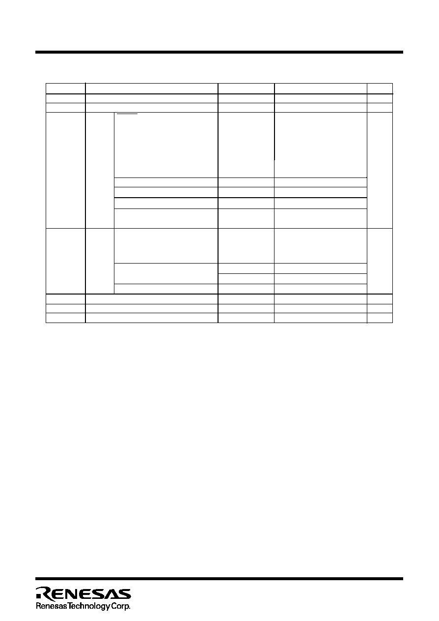
28
Electric characteristics (V
CC
= 5V)
Mitsubishi microcomputers
M30221 Group
SINGLE-CHIP 16-BIT CMOS MICROCOMPUTER
Table 1.21.1. Absolute maximum ratings
Operating ambient temperature
Parameter
Unit
Input
voltage
RESET, V
REF
, X
IN
Analog supply voltage
Supply voltage
Output
voltage
V
O
≠ 0.3 to Vcc+0.3
≠ 0.3 to Vcc+0.3
P
d
Power dissipation
Storage temperature
≠ 0.3 to 6.5
Rated value
≠ 0.3 to 6.5
V
V
V
Condition
V
I
AVcc
Vcc
T
stg
T
opr
Symbol
mW
V
≠ 40 to 150
300
≠ 20 to 85
P3
0
to P3
5
, P4
1
,P4
2
, P4
6
, P4
7
,
P0
0
to P0
7
, P1
0
to P1
7
, P2
0
to P2
7
,
P4
1
, P4
2
, P4
6
, P4
7
, P5
0
to P5
3
,
P1
0
to P1
7
, P2
0
to P2
7
, P3
0
to P3
5
,
Vcc=AVcc
Vcc=AVcc
P7
2
to P7
7
, P8
0
to P8
2
, P8
4
, P8
6
,
P9
0
to P9
6
, P10
0
to P10
3
,
VL1
P13
0
, P13
1
≠ 0.3 to VL2
VL2
VL1 to VL3
VL3
VL2 to 6.5
P7
0
, P7
1
, C1, C2
≠ 0.3 to 6.5
P5
6
, P5
7
, P6
0
to P6
3
, P7
2
to P7
6
,
P13
0
, P13
1
, X
OUT
P0
0
to P0
7
, P10
0
to P10
3
,
P11
0
to P11
7
, P12
0
to P12
5
≠ 0.3 to Vcc
When output port
When segment output
≠ 0.3 to VL3
P7
0
, P7
1
≠ 0.3 to 6.5
(Mask ROM version CNVss)
(flash memory version CNVss)
P11
0
to P11
7
, P12
0
to P12
5
,
Ta = 25∞C
∞C
∞C
P5
0
to P5
3
, P5
6
, P5
7
, P6
0
to P6
3
,
P8
0
to P8
2
, P8
4
, P8
6
, P9
0
to P9
6
,

29
Electric characteristics (V
CC
= 5V)
Mitsubishi microcomputers
M30221 Group
SINGLE-CHIP 16-BIT CMOS MICROCOMPUTER
Note 1: The mean output current is the mean value within 100ms.
Note 2: The total I
OL
(peak) for ports P0, P1, P2, P3
0
to P3
5
, P4, P5, P6, P7
0
to P7
6
and P12
2
to P12
7
must be 80mA max. The total
I
OH
(peak) for ports P0, P1, P2, P3
0
to P3
5
, P4, P5, P6, P7
2
to P7
6
and P12
2
to P12
7
must be 80mA max. The total I
OL
(peak)
for ports P8, P9, P10, P11, P12
0
, P12
1
and P13
0
to P13
2
must be 80mA max. The total I
OH
(peak) for ports P8, P9, P10, P11,
P12
0
,P12
1
and P13
0
to P13
2
must be 80mA max.
Note 3: Relationship between main clock oscillation frequency and supply voltage.
Table 1.21.2. Recommended operating conditions (referenced to V
CC
= 2.7V to 5.5V at Ta = ≠ 20 to 85
o
C
unless otherwise specified)
Typ.
Max.
Unit
Parameter
Vcc
Supply voltage
Symbol
Min.
Standard
f
(Xc
IN
)
Subclock oscillation frequency
kHz
50
32.768
V
Analog supply voltage
Vcc
AVcc
V
V
0
0
Analog supply voltage
Analog supply voltage
Vss
AVss
0.8Vcc
V
V
V
Vcc
0.2Vcc
0
LOW input
voltage
HIGH input
voltage
≠0.5
LOW peak
output current
10.0
f
(X
IN
)
Main clock input
oscillation frequency
MHz
I
OL (peak)
10
V
CC
=4.0V to 5.5V
With wait
5
X
V
CC
MHz
V
IH
V
IL
I
OH (avg)
HIGH average
output current
I
OH (peak)
HIGH peak
output current
I
OL (avg)
LOW average
output current
mA
mA
mA
2.5
P0
0
to P0
7
, P1
0
to P1
7
, P2
0
to P2
7
, P3
0
to P3
5
, P4
1
, P4
2
, P4
6
,
P0
0
to P0
7
, P10
0
to P10
3
, P11
0
to P11
7
, P12
0
to P12
5
5.0
0
0
V
CC
=2.7V to 4.0V
≠10.000
MHz
10
V
CC
=4.0V to 5.5V
2.31
X
V
CC
MHz
0
0
V
CC
=2.7V to 4.0V
+0.760
No wait
2.7
5.5
5.0
P7
0
, P7
1
0.8Vcc
6.5
P1
0
to P1
7
, P2
0
to P2
7
, P3
0
to P3
5
, P4
1
, P4
2
, P4
6
, P4
7
,
≠10.0
≠0.1
mA
≠5.0
5.0
(Note 1)
(Note 1)
(Note 3)
P4
7
, P5
0
to P5
3
, P5
6
, P5
7
, P6
0
to P6
3
, P7
2
to P7
7
, P8
0
to P8
2
,
P8
4
, P8
6
, P9
0
to P9
6
, P10
0
to P10
3
, P11
0
to P11
7
, P12
0
to P12
5
,
P5
0
to P5
3
, P5
6
, P5
7
, P6
0
to P6
3
, P7
2
to P7
6
, P8
0
to P8
2
, P8
4
,
P8
6
, P9
0
to P9
6
, P13
0
, P13
1
,
P13
0
, P13
1
, X
IN
, RESET, CNV
SS
P0
0
to P0
7
, P1
0
to P1
7
, P2
0
to P2
7
, P3
0
to P3
5
, P4
1
, P4
2
, P4
6
,
P4
7
, P5
0
to P5
3
, P5
6
, P5
7
, P6
0
to P6
3
, P7
0
to P7
7
, P8
0
to P8
2
,
P8
4
, P8
6
, P9
0
to P9
6
, P10
0
to P10
3
, P11
0
to P11
7
, P12
0
to P12
5
,
P13
0
, P13
1
, X
IN
, RESET, CNV
SS
P0
0
to P0
7
, P10
0
to P10
3
, P11
0
to P11
7
, P12
0
to P12
5
P1
0
to P1
7
, P2
0
to P2
7
, P3
0
to P3
5
, P4
1
, P4
2
, P4
6
, P4
7
,
P5
0
to P5
3
, P5
6
, P5
7
, P6
0
to P6
3
, P7
2
to P7
6
, P8
0
to P8
2
, P8
4
,
P8
6
, P9
0
to P9
6
, P13
0
, P13
1
,
P0
0
to P0
7
, P10
0
to P10
3
, P11
0
to P11
7
, P12
0
to P12
5
P1
0
to P1
7
, P2
0
to P2
7
, P3
0
to P3
5
, P4
1
, P4
2
, P4
6
, P4
7
,
P5
0
to P5
3
, P5
6
, P5
7
, P6
0
to P6
3
, P7
0
to P7
6
, P8
0
to P8
2
, P8
4
,
P8
6
, P9
0
to P9
6
, P13
0
, P13
1
,
P0
0
to P0
7
, P10
0
to P10
3
, P11
0
to P11
7
, P12
0
to P12
5
P1
0
to P1
7
, P2
0
to P2
7
, P3
0
to P3
5
, P4
1
, P4
2
, P4
6
, P4
7
,
P5
0
to P5
3
, P5
6
, P5
7
, P6
0
to P6
3
, P7
0
to P7
6
, P8
0
to P8
2
, P8
4
,
P8
6
, P9
0
to P9
6
, P13
0
, P13
1
,
(Note 2)
(Note 2)
5.5
4.0
2.7
0.0
3.5
10.0
Main clock input oscillation frequency
(No wait)
Supply voltage [V]
(BCLK: no division)
Operating maximum frequency [MH
Z
]
5 X Vcc≠10.000MHz
5.5
4.0
2.7
0.0
10.0
Main clock input oscillation frequency
(With wait)
Supply voltage [V]
(BCLK: no division)
7.0
2.31 X V
CC
+0.760MHz
Operating maximum frequency [MH
Z
]
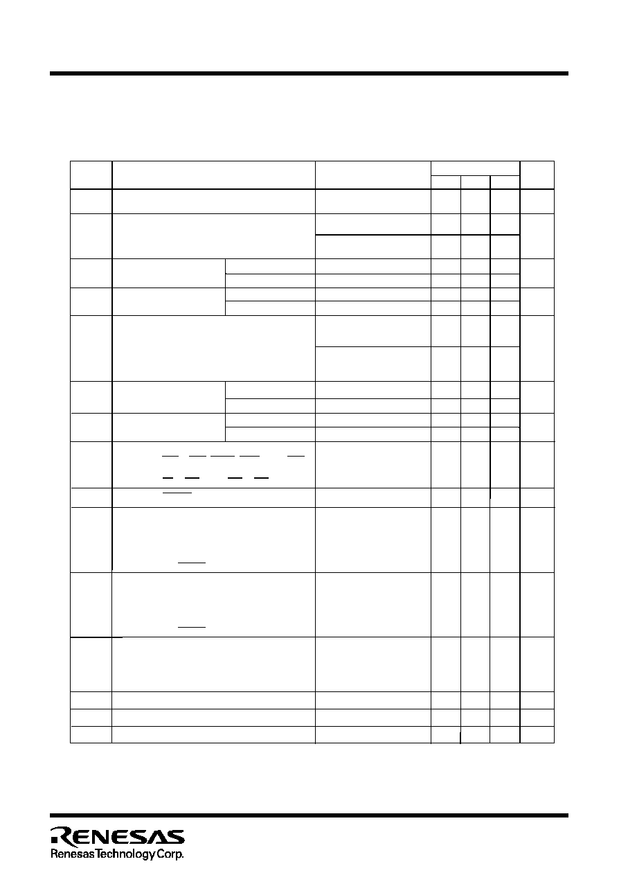
30
Electric characteristics (V
CC
= 5V)
Mitsubishi microcomputers
M30221 Group
SINGLE-CHIP 16-BIT CMOS MICROCOMPUTER
Table 1.21.3. Electrical characteristics (referenced to V
CC
= 5V, V
SS
= 0V at Ta = 25
o
C, f(X
IN
)=10MH
Z
unless otherwise specified)
V
CC
= 5V
Symbol
V
OH
V
OH
Feedback resistance X
CIN
HIGH output
voltage
HIGH output
voltage
Feedback resistance X
IN
P6
0
to P6
3
, P7
2
to P7
6
, P8
0
to P8
2
,
P0
0
to P0
7
, P1
0
to P1
7
, P2
0
to P2
7
,
P3
0
to P3
5
, P4
1
, P4
2
, P4
6
, P4
7
,
P8
4
, P8
6
,
P90
to P9
6
,
P130
, P13
1
P5
0
to P5
3
, P5
6
, P5
7
, P6
0
to P6
3
,
P7
0
to P7
6
, P8
0
to P8
2
, P8
4
, P8
6
,
P9
0
to P9
6
, P10
0
to P10
3
, P11
0
to P11
7
,
P12
0
to P12
5
, P13
0
, P13
1
Standard
Typ.
Unit
Measuring condition
V
4.7
INT
0
to INT
5
, AD
TRG
, CTS
0
, CLK
0
, NMI,
KI
0
to KI
15
(Note), KI
16
to KI
19
Min.
TA3
OUT
, TA4
OUT
, TA7
OUT
,
P0
0
to P0
7
, P1
0
to P1
7
, P2
0
to P2
7
,
P5
0
to P5
3
, P5
6
, P5
7
, P6
0
to P6
3
,
Max.
3.0
Parameter
I
OH
= ≠0.1mA
I
OH
= ≠5mA
P0
0
to P0
7
, P10
0
to P10
3
,
P11
0
to P11
7
, P12
0
to P12
5
P1
0
to P1
7
, P2
0
to P2
7
, P3
0
to P3
5
,
P4
1
, P4
2
, P4
6
, P4
7
, P5
0
to P5
3
, P5
6
, P5
7
,
V
V
OH
X
OUT
HIGH output
voltage
HIGHPOWER
LOWPOWER
V
3.0
3.0
I
OH
= ≠1mA
I
OH
= ≠0.5mA
V
OL
LOW output
voltage
V
2.0
I
OL
=5mA
V
OL
X
OUT
LOW output
voltage
HIGHPOWER
LOWPOWER
V
2.0
2.0
I
OH
=1mA
I
OH
=0.5mA
Hysteresis
Hysteresis
HIGH input
current
I
IH
V
T+-
V
T-
V
T+-
V
T-
0.2
0.8
V
0.2
1.8
V
5.0
µA
µA
RESET
TA0
IN
, TA3
IN
, TA4
IN
, TB0
IN
to TB3
IN
,
V
I
=5V
≠5.0
LOW input
current
I
IL
V
RAM
RAM retention voltage
When clock is stopped
2.0
V
V
I
=0V
V
OL
X
COUT
LOW output
voltage
HIGHPOWER
LOWPOWER
V
With no load applied
With no load applied
0
0
V
OH
X
COUT
HIGH output
voltage
HIGHPOWER
LOWPOWER
V
1.6
With no load applied
With no load applied
3.0
k
167.0
Pull-up
resistance
R
PULLUP
V
I
=0V
30.0
50.0
R
fXCIN
6.0
M
R
fXIN
1.0
M
I
OH
= ≠200µA
I
OL
=200µA
0.45
3.0
Note : Has no effect during intermittent pullup operation.
P3
0
to P3
5
, P4
1
, P4
2
, P4
6
, P4
7
,
P7
0
to P7
7
, P8
0
to P8
2
, P8
4
, P8
6
,
P9
0
to P9
6
, P10
0
to P10
3
, P11
0
to P11
7
,
P12
0
to P12
5
, P13
0
, P13
1
,
X
IN
, RESET, CNV
SS
P0
0
to P0
7
, P1
0
to P1
7
, P2
0
to P2
7
,
P5
0
to P5
3
, P5
6
, P5
7
, P6
0
to P6
3
,
P3
0
to P3
5
, P4
1
, P4
2
, P4
6
, P4
7
,
P7
0
to P7
7
, P8
0
to P8
2
, P8
4
, P8
6
,
P9
0
to P9
6
, P10
0
to P10
3
, P11
0
to P11
7
,
P12
0
to P12
5
, P13
0
, P13
1
,
X
IN
, RESET, CNV
SS
P0
0
to P0
7
, P1
0
to P1
7
, P2
0
to P2
7
,
P5
0
to P5
3
, P5
6
, P5
7
, P6
0
to P6
3
,
P3
0
to P3
5
, P4
1
, P4
2
, P4
6
, P4
7
,
P7
2
to P7
6
, P8
0
to P8
2
, P8
4
, P8
6
,
P9
0
to P9
6
, P10
0
to P10
3
, P11
0
to P11
7
,
P12
0
to P12
5
, P13
0
, P13
1
,
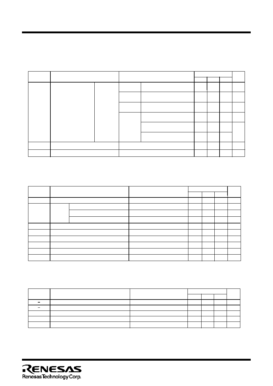
31
Electric characteristics (V
CC
= 5V)
Mitsubishi microcomputers
M30221 Group
SINGLE-CHIP 16-BIT CMOS MICROCOMPUTER
Table 1.21.5. A-D conversion characteristics (referenced to V
CC
= AV
CC
= V
REF
= 5V, Vss = AV
SS
= 0V
at Ta = 25
o
C, f(X
IN
) = 10MH
Z
unless otherwise specified)
V
CC
= 5V
Symbol
Standard
Typ.
Unit
Measuring condition
Min.
Max.
Parameter
Icc
Power supply current
Square wave, no division
When clock is stopped
Ta=25 ∫C
1.0
µA
mA
Ta=85 ∫C
20.0
When clock is stopped
19.0
38.0
f(X
IN
)=10MHz
f(X
CIN
)=32kHz
When a WAIT instruction is executed
4.0
µA
I/o pin is no
load applied
f(X
CIN
)=32kHz
Square wave
90.0
µA
V
L1
Supply voltage (VL1)
When voltage multiplier used
V
1.3
2.1
1.7
I
L1
Power supply current (VL1)
VL1=1.7V,f(
LCDCK
)=200Hz
6.0
µA
3.0
f(X
CIN
)=32kHz
Square wave
Mask ROM
version
Flash memory
version
200.0
µA
Standard
Min.
Typ. Max.
≠
≠
Resolution
Absolute
accuracy
Bits
LSB
V
REF
=V
CC
±3
10
Symbol
Parameter
Measuring condition
Unit
V
REF
=V
CC
= 5V
R
LADDER
t
CONV
Ladder resistance
Conversion time
(10bit)
Reference voltage
Analog input voltage
k
µs
V
V
IA
V
REF
V
0
2
10
V
CC
V
REF
40
3.3
Conversion time
(8bit)
µs
2.8
t
CONV
t
SAMP
Sampling time
0.3
µs
V
REF
=V
CC
Sample & hold function not available
Sample & hold function available(10bit)
V
REF
=V
CC
= 5V
LSB
±3
Sample & hold function available(8bit)
V
REF
= V
CC
= 5V
±2
LSB
Min.
Typ.
Max.
t
su
R
O
Resolution
Absolute accuracy
Setup time
Output resistance
Reference power supply input current
Bits
%
k
mA
I
VREF
1.0
1.5
8
3
Symbol
Parameter
Measuring condition
Unit
20
10
4
µs
(
Note
)
Standard
Table 1.21.4. Electrical characteristics (referenced to V
CC
= 5V, V
SS
= 0V at Ta = 25
o
C, f(X
IN
)=10MH
Z
unless otherwise specified)
Table 1.21.6. D-A conversion characteristics (referenced to V
CC
= AV
CC
=V
REF
=5V, V
SS
= AV
SS =
0V at Ta = 25
o
C, f(X
IN
) = 10MH
Z
unless otherwise specified)
Note: This applies when using one D-A converter, with the D-A register for the unused D-A converter set to "00
16
".
The A-D converter's ladder resistance is not included.
Also, when the Vref is unconnected at the A-D control register, I
VREF
is sent.
32
Timing (V
CC
= 5V)
Mitsubishi microcomputers
M30221 Group
SINGLE-CHIP 16-BIT CMOS MICROCOMPUTER
Timing requirements (referenced to V
CC
= 5V, V
SS
= 0V at Ta = 25
o
C unless otherwise specified)
Table 1.21.7. External clock input
Table 1.21.9. Timer A input (gating input in timer mode)
Table 1.21.10. Timer A input (external trigger input in one-shot timer mode)
Table 1.21.11. Timer A input (external trigger input in pulse width modulation mode)
Table 1.21.12. Timer A input (up/down input in event counter mode)
V
CC
= 5V
Max.
External clock rise time
ns
t
r
Min.
External clock input cycle time
External clock input HIGH pulse width
External clock input LOW pulse width
External clock fall time
ns
ns
ns
ns
t
c
t
w(H
)
t
w(L)
t
f
Parameter
Symbol
Unit
Standard
15
100
40
40
15
Standard
Max.
ns
TAi
IN
input LOW pulse width
t
w(TAL)
Min.
ns
ns
Unit
TAi
IN
input HIGH pulse width
t
w(TAH)
Parameter
Symbol
t
c(TA)
TAi
IN
input cycle time
40
100
40
Standard
Max.
Min.
ns
ns
ns
Unit
TAi
IN
input cycle time
TAi
IN
input HIGH pulse width
TAi
IN
input LOW pulse width
t
c(TA)
t
w(TAH)
t
w(TAL)
Symbol
Parameter
400
200
200
Standard
Max.
Min.
ns
ns
ns
Unit
TAi
IN
input cycle time
TAi
IN
input HIGH pulse width
TAi
IN
input LOW pulse width
t
c(TA)
t
w(TAH)
t
w(TAL)
Symbol
Parameter
200
100
100
Standard
Max.
Min.
ns
ns
Unit
t
w(TAH)
t
w(TAL)
Symbol
Parameter
TAi
IN
input HIGH pulse width
TAi
IN
input LOW pulse width
100
100
Standard
Max.
Min.
ns
ns
ns
Unit
ns
ns
Symbol
Parameter
TAi
OUT
input cycle time
TAi
OUT
input HIGH pulse width
TAi
OUT
input LOW pulse width
TAi
OUT
input setup time
TAi
OUT
input hold time
t
c(UP)
t
w(UPH)
t
w(UPL)
t
su(UP-T
IN
)
t
h(T
IN-
UP)
2000
1000
1000
400
400
Table 1.21.8. Timer A input (counter input in event counter mode)
33
Timing (V
CC
= 5V)
Mitsubishi microcomputers
M30221 Group
SINGLE-CHIP 16-BIT CMOS MICROCOMPUTER
Timing requirements (referenced to V
CC
= 5V, V
SS
= 0V at Ta = 25
o
C unless otherwise specified)
Table 1.21.13. Timer B input (counter input in event counter mode)
Table 1.21.14. Timer B input (pulse period measurement mode)
Table 1.21.15. Timer B input (pulse width measurement mode)
Table 1.21.16. A-D trigger input
Table 1.21.17. Serial I/O
_______
Table 1.21.18. External interrupt INTi inputs
V
CC
= 5V
Standard
Max.
Min.
TBi
IN
input cycle time (counted on one edge)
TBi
IN
input HIGH pulse width (counted on one edge)
TBi
IN
input LOW pulse width (counted on one edge)
ns
ns
ns
t
c(TB)
t
w(TBH)
t
w(TBL)
Parameter
Symbol
Unit
t
c(TB)
t
w(TBL)
t
w(TBH)
ns
ns
ns
TBi
IN
input HIGH pulse width (counted on both edges)
TBi
IN
input LOW pulse width (counted on both edges)
TBi
IN
input cycle time (counted on both edges)
Standard
Max.
Min.
ns
ns
t
c(TB)
t
w(TBH)
Symbol
Parameter
Unit
t
w(TBL)
ns
TBi
IN
input HIGH pulse width
TBi
IN
input cycle time
TBi
IN
input LOW pulse width
Standard
Max.
Min.
ns
ns
t
c(TB)
Symbol
Parameter
Unit
t
w(TBL)
ns
t
w(TBH)
TBi
IN
input cycle time
TBi
IN
input HIGH pulse width
TBi
IN
input LOW pulse width
Standard
Max.
Min.
ns
ns
t
c(AD)
t
w(ADL)
Symbol
Parameter
Unit
AD
TRG
input cycle time (trigger able minimum)
AD
TRG
input LOW pulse width
100
40
40
80
80
200
400
200
200
400
200
200
1000
125
ns
ns
ns
ns
ns
ns
ns
Standard
Max.
Min.
ns
ns
t
w(INH)
t
w(INL)
Symbol
Parameter
Unit
INTi input LOW pulse width
INTi input HIGH pulse width
Standard
Max.
Min.
CLKi input cycle time
CLKi input HIGH pulse width
CLKi input LOW pulse width
t
c(CK)
t
w(CKH)
t
w(CKL)
Parameter
Symbol
Unit
t
d(C-Q)
t
su(D-C)
t
h(C-Q)
TxDi hold time
RxDi input setup time
TxDi output delay time
t
h(C-D)
RxDi input hold time
250
250
200
100
100
0
30
90
80
34
Timing (V
CC
= 5V)
Mitsubishi microcomputers
M30221 Group
SINGLE-CHIP 16-BIT CMOS MICROCOMPUTER
Figure 1.21.1. Port P0 to P13 measurement circuit
P6
P7
P8
P10
P9
P0
P1
P2
P3
P4
P5
30pF
P11
P12
P13
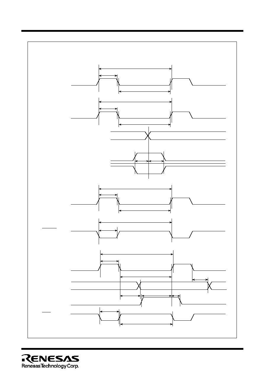
35
Timing (V
CC
= 5V)
Mitsubishi microcomputers
M30221 Group
SINGLE-CHIP 16-BIT CMOS MICROCOMPUTER
t
su(D≠C)
TAi
IN
input
TAi
OUT
input
During event counter mode
TBi
IN
input
CLKi
TxDi
RxDi
t
c(TA)
t
w(TAH)
t
w(TAL)
t
c(UP)
t
w(UPH)
t
w(UPL)
t
c(TB)
t
w(TBH)
t
w(TBL)
t
c(AD)
t
w(ADL)
t
c(CK)
t
w(CKH)
t
w(CKL)
t
w(INL)
t
w(INH)
t
d(C≠Q)
t
h(C≠D)
t
h(C≠Q)
t
h(T
IN
≠UP)
t
su(UP≠T
IN
)
TAi
IN
input
(When count on falling
edge is selected)
TAi
IN
input
(When count on rising
edge is selected)
TAi
OUT
input
(Up/down input)
INTi input
AD
TRG
input
V
CC
= 5V
36
Electric characteristics (V
CC
= 3V)
Mitsubishi microcomputers
M30221 Group
SINGLE-CHIP 16-BIT CMOS MICROCOMPUTER
V
CC
= 3V
Table 1.21.19. Electrical characteristics (referenced to V
CC
= 3V, V
SS
= 0V at Ta = 25
o
C, f(X
IN
) =
7MH
Z
, with wait)
Symbol
V
OH
V
OH
Feedback resistance X
CIN
HIGH output
voltage
HIGH output
voltage
Feedback resistance X
IN
P6
0
to P6
3
, P7
2
to P7
6
, P8
0
to P8
2
,
P0
0
to P0
7
, P1
0
to P1
7
, P2
0
to P2
7
,
P3
0
to P3
5
, P4
1
, P4
2
, P4
6
, P4
7
,
P8
4
, P8
6
,
P90
to P9
6
,
P130
, P13
1
P5
0
to P5
3
, P5
6
, P5
7
, P6
0
to P6
3
,
P7
0
to P7
6
, P8
0
to P8
2
, P8
4
, P8
6
,
P9
0
to P9
6
, P10
0
to P10
3
, P11
0
to P11
7
,
P12
0
to P12
5
, P13
0
, P13
1
Standard
Typ.
Unit
Measuring condition
INT
0
to INT
5
, AD
TRG
, CTS
0
, CLK
0
, NMI,
KI
0
to KI
15
(Note), KI
16
to KI
19
Min.
TA3
OUT
, TA4
OUT
, TA7
OUT
,
P0
0
to P0
7
, P1
0
to P1
7
, P2
0
to P2
7
,
P5
0
to P5
3
, P5
6
, P5
7
, P6
0
to P6
3
,
Max.
Parameter
P0
0
to P0
7
, P10
0
to P10
3
,
P11
0
to P11
7
, P12
0
to P12
5
P1
0
to P1
7
, P2
0
to P2
7
, P3
0
to P3
5
,
P4
1
, P4
2
, P4
6
, P4
7
, P5
0
to P5
3
, P5
6
, P5
7
,
V
OH
X
OUT
HIGH output
voltage
HIGHPOWER
LOWPOWER
V
OL
LOW output
voltage
V
OL
X
OUT
LOW output
voltage
HIGHPOWER
LOWPOWER
Hysteresis
Hysteresis
HIGH input
current
I
IH
V
T+-
V
T-
V
T+-
V
T-
RESET
TA0
IN
, TA3
IN
, TA4
IN
, TB0
IN
to TB3
IN
,
LOW input
current
I
IL
V
RAM
RAM retention voltage
V
OL
X
COUT
LOW output
voltage
HIGHPOWER
LOWPOWER
V
OH
X
COUT
HIGH output
voltage
HIGHPOWER
LOWPOWER
Pull-up
resistance
R
PULLUP
R
fXCIN
R
fXIN
Note : Has no effect during intermittent pullup operation.
P3
0
to P3
5
, P4
1
, P4
2
, P4
6
, P4
7
,
P7
0
to P7
7
, P8
0
to P8
2
, P8
4
, P8
6
,
P9
0
to P9
6
, P10
0
to P10
3
, P11
0
to P11
7
,
P12
0
to P12
5
, P13
0
, P13
1
,
X
IN
, RESET, CNV
SS
P0
0
to P0
7
, P1
0
to P1
7
, P2
0
to P2
7
,
P5
0
to P5
3
, P5
6
, P5
7
, P6
0
to P6
3
,
P3
0
to P3
5
, P4
1
, P4
2
, P4
6
, P4
7
,
P7
0
to P7
7
, P8
0
to P8
2
, P8
4
, P8
6
,
P9
0
to P9
6
, P10
0
to P10
3
, P11
0
to P11
7
,
P12
0
to P12
5
, P13
0
, P13
1
,
X
IN
, RESET, CNV
SS
P0
0
to P0
7
, P1
0
to P1
7
, P2
0
to P2
7
,
P5
0
to P5
3
, P5
6
, P5
7
, P6
0
to P6
3
,
P3
0
to P3
5
, P4
1
, P4
2
, P4
6
, P4
7
,
P7
2
to P7
6
, P8
0
to P8
2
, P8
4
, P8
6
,
P9
0
to P9
6
, P10
0
to P10
3
, P11
0
to P11
7
,
P12
0
to P12
5
, P13
0
, P13
1
,
V
2.0
I
OH
= ≠20µA
I
OH
= ≠1mA
V
V
2.5
2.5
I
OH
= ≠0.1mA
I
OH
= ≠50µA
V
0.5
I
OL
=1mA
V
0.5
0.5
I
OH
=0.1mA
I
OH
=50µA
0.2
0.8
V
0.2
1.8
V
4.0
µA
µA
V
I
=3V
≠4.0
When clock is stopped
2.0
V
V
I
=0V
V
With no load applied
With no load applied
0
0
V
1.6
With no load applied
With no load applied
3.0
k
500.0
V
I
=0V
66.0
120.0
10.0
M
3.0
M
2.5
37
Electric characteristics (V
CC
= 3V)
Mitsubishi microcomputers
M30221 Group
SINGLE-CHIP 16-BIT CMOS MICROCOMPUTER
V
CC
= 3V
Table 1.21.22. D-A conversion characteristics (referenced to V
CC
= AV
CC
= V
REF
= 3V, V
SS
= AV
SS =
0V, at Ta = 25
o
C, f(X
IN
) = 7MH
Z
unless otherwise specified)
Note : This applies when using one D-A converter, with the D-A register for the unused D-A converter set to "00
16
". The
A-D converter's ladder resistance is not included.
Also, when the Vref is unconnected at the A-D control register, IV
REF
is sent.
Table 1.21.21. A-D conversion characteristics (referenced to V
CC
= AV
CC
= V
REF
= 3V, V
SS
= AV
SS
=
0V at Ta = 25
o
C, f(X
IN
) = 7MH
Z
, with wait unless otherwise specified)
Symbol
Standard
Typ.
Unit
Measuring condition
Min.
Max.
Parameter
Icc
Power supply current
Square wave, no division
When clock is stopped
Ta=25 ∫C
1.0
µA
mA
Ta=85 ∫C
20.0
When clock is stopped
6.0
15.0
f(X
IN
)=7MHz
f(X
CIN
)=32kHz
When a WAIT instruction is executed
Oscillation capacity High (Note)
2.8
µA
I/o pin is no
load applied
f(X
CIN
)=32kHz
Square wave
40.0
µA
V
L1
Supply voltage (VL1)
When voltage multiplier used
V
1.3
2.1
1.7
I
L1
Power supply current (VL1)
VL1=1.7V,f(
LCDCK
)=200Hz
6.0
µA
3.0
f(X
CIN
)=32kHz
Square wave
Mask ROM
version
Flash memory
version
150.0
µA
f(X
CIN
)=32kHz
When a WAIT instruction is executed
Oscillation capacity Low (Note)
0.9
µA
Note: With one timer operated using f
C32
.
Standard
≠
≠
Resolution
Absolute
accuracy
Bits
LSB
V
REF
=V
CC
±2
10
Symbol
Parameter
Measuring condition
V
REF
=V
CC
= 3V,
AD
=f
AD
/2
R
LADDER
Ladder resistance
Reference voltage
Analog input voltage
k
V
V
IA
V
REF
V
0
2.7
10
V
CC
V
REF
40
Conversion time
(8bit)
µs
14.0
t
CONV
V
REF
=V
CC
Sample & hold function not available
(8bit)
Min.
Typ. Max.
Unit
Min.
Typ.
Max.
t
su
R
O
Resolution
Absolute accuracy
Setup time
Output resistance
Reference power supply input current
Bits
%
k
mA
I
VREF
1.0
1.0
8
3
Symbol
Parameter
Measuring condition
Unit
20
10
4
µs
(
Note
)
Standard
Table 1.21.20. Electrical characteristics (referenced to V
CC
= 3V, V
SS
= 0V at Ta = 25
o
C, f(X
IN
) =
7MH
Z
, with wait)
38
Timing (V
CC
= 3V)
Mitsubishi microcomputers
M30221 Group
SINGLE-CHIP 16-BIT CMOS MICROCOMPUTER
Table 1.21.25. Timer A input (gating input in timer mode)
Table 1.21.26. Timer A input (external trigger input in one-shot timer mode)
Table 1.21.27. Timer A input (external trigger input in pulse width modulation mode)
Table 1.21.28. Timer A input (up/down input in event counter mode)
Table 1.21.24. Timer A input (counter input in event counter mode)
Timing requirements (referenced to V
CC
= 3V, V
SS
= 0V at Ta = 25
o
C unless otherwise specified)
V
CC
= 3V
Table 1.21.23. External clock input
Max.
External clock rise time
ns
t
r
Min.
External clock input cycle time
External clock input HIGH pulse width
External clock input LOW pulse width
External clock fall time
ns
ns
ns
ns
t
c
t
w(H
)
t
w(L)
t
f
Parameter
Symbol
Unit
Standard
18
143
60
60
18
Standard
Max.
ns
TAi
IN
input LOW pulse width
t
w(TAL)
Min.
ns
ns
Unit
TAi
IN
input HIGH pulse width
t
w(TAH)
Parameter
Symbol
t
c(TA)
TAi
IN
input cycle time
60
150
60
Standard
Max.
Min.
ns
ns
ns
Unit
TAi
IN
input cycle time
TAi
IN
input HIGH pulse width
TAi
IN
input LOW pulse width
t
c(TA)
t
w(TAH)
t
w(TAL)
Symbol
Parameter
600
300
300
Standard
Max.
Min.
ns
ns
ns
Unit
TAi
IN
input cycle time
TAi
IN
input HIGH pulse width
TAi
IN
input LOW pulse width
t
c(TA)
t
w(TAH)
t
w(TAL)
Symbol
Parameter
300
150
150
Standard
Max.
Min.
ns
ns
Unit
t
w(TAH)
t
w(TAL)
Symbol
Parameter
TAi
IN
input HIGH pulse width
TAi
IN
input LOW pulse width
150
150
Standard
Max.
Min.
ns
ns
ns
Unit
ns
ns
Symbol
Parameter
TAi
OUT
input cycle time
TAi
OUT
input HIGH pulse width
TAi
OUT
input LOW pulse width
TAi
OUT
input setup time
TAi
OUT
input hold time
t
c(UP)
t
w(UPH)
t
w(UPL)
t
su(UP-T
IN
)
t
h(T
IN-
UP)
3000
1500
1500
600
600
39
Timing (V
CC
= 3V)
Mitsubishi microcomputers
M30221 Group
SINGLE-CHIP 16-BIT CMOS MICROCOMPUTER
Timing requirements (referenced to V
CC
= 3V, V
SS
= 0V at Ta = 25
o
C unless otherwise specified)
V
CC
= 3V
Table 1.21.29. Timer B input (counter input in event counter mode)
Table 1.21.30. Timer B input (pulse period measurement mode)
Table 1.21.31. Timer B input (pulse width measurement mode)
Table 1.21.32. A-D trigger input
Table 1.21.33. Serial I/O
_______
Table 1.21.34. External interrupt INTi inputs
Standard
Max.
Min.
TBi
IN
input cycle time (counted on one edge)
TBi
IN
input HIGH pulse width (counted on one edge)
TBi
IN
input LOW pulse width (counted on one edge)
ns
ns
ns
t
c(TB)
t
w(TBH)
t
w(TBL)
Parameter
Symbol
Unit
t
c(TB)
t
w(TBL)
t
w(TBH)
ns
ns
ns
TBi
IN
input HIGH pulse width (counted on both edges)
TBi
IN
input LOW pulse width (counted on both edges)
TBi
IN
input cycle time (counted on both edges)
Standard
Max.
Min.
ns
ns
t
c(TB)
t
w(TBH)
Symbol
Parameter
Unit
t
w(TBL)
ns
TBi
IN
input HIGH pulse width
TBi
IN
input cycle time
TBi
IN
input LOW pulse width
Standard
Max.
Min.
ns
ns
t
c(TB)
Symbol
Parameter
Unit
t
w(TBL)
ns
t
w(TBH)
TBi
IN
input cycle time
TBi
IN
input HIGH pulse width
TBi
IN
input LOW pulse width
Standard
Max.
Min.
ns
ns
t
c(AD)
t
w(ADL)
Symbol
Parameter
Unit
AD
TRG
input cycle time (trigger able minimum)
AD
TRG
input LOW pulse width
150
60
60
160
160
300
600
300
300
600
300
300
1500
200
ns
ns
ns
ns
ns
ns
ns
Standard
Max.
Min.
ns
ns
t
w(INH)
t
w(INL)
Symbol
Parameter
Unit
INTi input LOW pulse width
INTi input HIGH pulse width
Standard
Max.
Min.
CLKi input cycle time
CLKi input HIGH pulse width
CLKi input LOW pulse width
t
c(CK)
t
w(CKH)
t
w(CKL)
Parameter
Symbol
Unit
t
d(C-Q)
t
su(D-C)
t
h(C-Q)
TxDi hold time
RxDi input setup time
TxDi output delay time
t
h(C-D)
RxDi input hold time
380
380
300
150
150
0
50
90
160

40
Timing (V
CC
= 3V)
Mitsubishi microcomputers
M30221 Group
SINGLE-CHIP 16-BIT CMOS MICROCOMPUTER
V
CC
= 3V
t
su(D≠C)
TAi
IN
input
TAi
OUT
input
During event counter mode
TBi
IN
input
CLKi
TxDi
RxDi
t
c(TA)
t
w(TAH)
t
w(TAL)
t
c(UP)
t
w(UPH)
t
w(UPL)
t
c(TB)
t
w(TBH)
t
w(TBL)
t
c(AD)
t
w(ADL)
t
c(CK)
t
w(CKH)
t
w(CKL)
t
w(INL)
t
w(INH)
t
d(C≠Q)
t
h(C≠D)
t
h(C≠Q)
t
h(T
IN
≠UP)
t
su(UP≠T
IN
)
TAi
IN
input
(When count on falling
edge is selected)
TAi
IN
input
(When count on rising
edge is selected)
TAi
OUT
input
(Up/down input)
INTi input
AD
TRG
input

41
Usage precaution peculiar to M30221 Group
Mitsubishi microcomputers
M30221 Group
SINGLE-CHIP 16-BIT CMOS MICROCOMPUTER
Usage precaution against the differences between M30220 Group and M30221 Group
Deleted pins from M30220 Group
Port
Deleted pin name
P0
-
P1
P2
P3
P4
P5
P6
P7
P8
P9
P10
P11
P12
P13
others
-
-
-
P4
0
/TA0
OUT
P4
3
/TA1
IN
P4
4
/TA2
OUT
P4
5
/TA2
IN
P5
4
/TB4
IN
P5
5
/TB5
IN
P6
4
/CTS
1
/RTS
1
/CLKS
1
P6
5
/CLK
1
P6
6
/R
X
D
1
P6
7
/T
X
D
1
-
P8
3
/TA5
IN
P8
5
/TA6
IN
P8
7
/TA7
IN
P9
7
/AN
7
P10
4
/SEG
20
P10
5
/SEG
21
P10
6
/SEG
22
P10
7
/SEG
23
-
P12
6
/SEG
38
P12
7
/SEG
39
P13
2
/DA
2
SEG
0
SEG
1
VSS(1 pin)
Differences between M30220 Group and M30221 Group
Items
ROM (Byte)
RAM (Byte)
Input only / Output only
CMOS I/O
N-channel open-drain
Internal
Memory
I/O
Ports
DMAC (channels)
16-bit timers
CRC Operation Circuit
Clock Sync. / UART
Clock Synchronous
UART only
Serial
I/O
A-D Converter (resolution ◊ channels)
D-A Converter (resolution ◊ channels)
External Interrupts (source)
Watchdog Timer
Segment (lines)
Common (lines)
Charge pump
LCD
Controller
/ Driver
Real Time Output Ports (bits ◊ ports)
Key-on Wake up (lines)
Number of Basic Instructions
Minimum Instruction Excution Time (ns)
Operating Temperature Range ()
Sub Clock Generating Circuit
Packages
Power Source Voltage (V)
M30220 Group
M30221 Group
128K
**
10K
**
128K
**
10K
**
96K
6K
64K
***
4K
***
64K
***
4K
***
24K
1.5K
Input only : 1 / Output only : 16 (shared with LCD outputs)
Input only : 1 / Output only : 14 (shared with LCD outputs)
102 (32 lines are shared with LCD outputs)
2
8+6
3
10bits◊8
8
Available
48
4
8◊4
Max.20 (16 lines have Intermittent pull-up operation)
144-pin TQFP (144PFB-A)
144-pin LQFP (144P6Q-A)
2.7 to 5.5 (7MHz with 1wait) 4.0 to 5.5 (10MHz)
-20 to 85-40 to 85
100 (10MHz)
91
2
-
-
-
2
10bits◊7
8bits◊3
8bits◊2
Available
Available
8◊3, 6◊1
120-pin LQFP (120P6R-A)
40
81 (26 lines are shared with LCD outputs)
Under developmentUnder planning (April. 2001)
32K
***
2K
***
42
Usage precaution peculiar to M30221 Group
Mitsubishi microcomputers
M30221 Group
SINGLE-CHIP 16-BIT CMOS MICROCOMPUTER
(1)UART1 is not available.
Usage precaution against serial I/O
Usage precaution against timer B
Mode
Function
Timer B4 and B5 are not available.
Not available timer Bi
Event counter
mode
Count source input
Pulse period
/ pulse width
measurement
mode
Timer B4 and B5 are not available.
(1)Pins P12
6
and P12
7
are deleted.
Usage precaution against real time port outputs
(1)Pins SEG
0
, SEG
1
, SEG
20
to SEG
23
, SEG
38
and SEG
39
are deleted.
(2)Addresses of the designated RAM for the LCD display 0100
16
, 010A
16
, 010B
16
and 0113
16
are reserved area.
(3)Bit 5 of the segment output enable register (address 0122
16
) is reserved bit. Must always be clear to "0".
Usage precaution against LCD controller / driver
Usage precaution against timer A
Mode
Function
Timer mode
Pulse output
Timer A0 and A2 are not available.
Not available timer Ai
One-shot timer
mode
Timer A1 , A2 , and A5 to A7 are not available.
Gate input
Event counter
mode
Pulse output
Timer A0 and A2 are not available.
Count source input
Timer A1 , A2 , and A5 to A7 are not available.
Up / down count select input
Timer A0 and A2 are not available.
Two-phase pulse input
Pulse output
Trigger input
Timer A0 and A2 are not available.
Timer A1 , A2 , and A5 to A7 are not available.
Pulse width
modulation mode Trigger input
Timer A0 and A2 are not available.
Timer A1 and A5 to A7 are not available.
Note 1Timer A3 and A4 are available.
Timer A2 and A7 are not available.(Note 1)
43
Usage precaution peculiar to M30221 Group
Mitsubishi microcomputers
M30221 Group
SINGLE-CHIP 16-BIT CMOS MICROCOMPUTER
Usage precaution against A-D converter
(1)AN
7
pin is deleted.
(2)Do not set the analog input pin select bit (bit 0 to 2 at address 03D6
16
) to "111" in one-shot mode and in repeat
mode.
(3)When the A-D sweep pin select bit (bit 0 , 1 at address 03D7
16
) is set to "11" in single sweep mode , the
interrupt request generation timing of the A-D conversion is the A-D conversion time of all 8 pins.
(4)The sweep time is the A-D conversion time of all 8 pins in repeat sweep mode 1 and when the A-D sweep pin
select bit (bit 0 , 1 at address 03D7
16
) is set to "11" in repeat sweep mode 0.
Usage precaution against D-A converter
(1)DA
2
pin is deleted.
(2)Bit 2 of the D-A control register (address 03DC
16
) is reserved bit. Must always be clear to "0".
(3)Address 03DE
16
must always be clear to "00
16
".
Usage precaution against programmable I/O
(1)Reserved bits of the port Pi direction register and the port Pi register
Register
Bit
PD0P0
-
-
-
-
PD1P1
PD2P2
PD3P3
PD4P4
PD5P5
PD6P6
Register
Bit
PD7P7
PD8P8
PD9P9
PD10P10
PD11P11
PD12P12
PD13P13
b0b3b5(Note 1)
b4b5(Note 1)
b4b7(Note 1)
-
b3b5b7(Note 1)
b7(Note 1)
b4b7(Note 1)
b6b7(Note 1)
b2(Note 1)
-
Note 1These are reserved bits. Must always be clear to "0".
(2)Reserved bits of the pull-up control register
Bit 5 of the pull-up control register 1 (address 03FD
16
) and bit 5 of the pull-up control register 2 (address 03FE
16
)
are reserved bits. Must always be clear to "0".

Keep safety first in your circuit designs!
Notes regarding these materials
q
Mitsubishi Electric Corporation puts the maximum effort into making semiconductor
products better and more reliable, but there is always the possibility that trouble may
occur with them. Trouble with semiconductors may lead to personal injury, fire or
property damage. Remember to give due consideration to safety when making your
circuit designs, with appropriate measures such as (i) placement of substitutive,
auxiliary circuits, (ii) use of non-flammable material or (iii) prevention against any
malfunction or mishap.
q
These materials are intended as a reference to assist our customers in the selection
of the Mitsubishi semiconductor product best suited to the customer's application;
they do not convey any license under any intellectual property rights, or any other
rights, belonging to Mitsubishi Electric Corporation or a third party.
q
Mitsubishi Electric Corporation assumes no responsibility for any damage, or
infringement of any third-party's rights, originating in the use of any product data,
diagrams, charts, programs, algorithms, or circuit application examples contained in
these materials.
q
All information contained in these materials, including product data, diagrams, charts,
programs and algorithms represents information on products at the time of publication
of these materials, and are subject to change by Mitsubishi Electric Corporation
without notice due to product improvements or other reasons. It is therefore
recommended that customers contact Mitsubishi Electric Corporation or an authorized
Mitsubishi Semiconductor product distributor for the latest product information before
purchasing a product listed herein.
The information described here may contain technical inaccuracies or typographical
errors. Mitsubishi Electric Corporation assumes no responsibility for any damage,
liability, or other loss rising from these inaccuracies or errors.
Please also pay attention to information published by Mitsubishi Electric Corporation
by various means, including the Mitsubishi Semiconductor home page (http://
www.mitsubishichips.com).
q
When using any or all of the information contained in these materials, including
product data, diagrams, charts, programs, and algorithms, please be sure to evaluate
all information as a total system before making a final decision on the applicability of
the information and products. Mitsubishi Electric Corporation assumes no
responsibility for any damage, liability or other loss resulting from the information
contained herein.
q
Mitsubishi Electric Corporation semiconductors are not designed or manufactured
for use in a device or system that is used under circumstances in which human life is
potentially at stake. Please contact Mitsubishi Electric Corporation or an authorized
Mitsubishi Semiconductor product distributor when considering the use of a product
contained herein for any specific purposes, such as apparatus or systems for
transportation, vehicular, medical, aerospace, nuclear, or undersea repeater use.
q
The prior written approval of Mitsubishi Electric Corporation is necessary to reprint
or reproduce in whole or in part these materials.
q
If these products or technologies are subject to the Japanese export control
restrictions, they must be exported under a license from the Japanese government
and cannot be imported into a country other than the approved destination.
Any diversion or reexport contrary to the export control laws and regulations of Japan
and/or the country of destination is prohibited.
q
Please contact Mitsubishi Electric Corporation or an authorized Mitsubishi Semicon
ductor product distributor for further details on these materials or the products con
tained therein.

MITSUBISHI SEMICONDUCTORS
M30221 Group Specification REV.D
May. First Edition 2001
Editioned by
Committee of editing of Mitsubishi Semiconductor
Published by
Mitsubishi Electric Corp., Kitaitami Works
This book, or parts thereof, may not be reproduced in any form without
permission of Mitsubishi Electric Corporation.
©2001 MITSUBISHI ELECTRIC CORPORATION