Rev.0.80
Mar 18, 2005
Page 1 of 34
REJ03B0088-0080
PRELIMINARY
M16C/30P Group
SINGLE-CHIP 16-BIT CMOS MICROCOMPUTER
Notice: This is not a final specification.
Some parametric limits are subject to change.
REJ03B0088-0080
Rev.0.80
Mar 18, 2005
1.
Overview
The M16C/30P Group of single-chip microcomputers are built using the high-performance silicon gate CMOS process
using a M16C/60 Series CPU core and are packaged in a 100-pin plastic molded QFP.
These single-chip microcomputers operate using sophisticated instructions featuring a high level of instruction
efficiency. With 1M bytes of address space, they are capable of executing instructions at high speed. In addition, this
microcomputer contains a multiplier and DMAC which combined with fast instruction processing capability, makes it
suitable for control of various OA, communication, and industrial equipment which requires high-speed arithmetic/
logic operations.
1.1
Applications
Audio, cameras, TV, home appliance, office/communications/portable/industrial equipment, etc.
Specifications written in this manual are believed to be accurate,
but are not guaranteed to be entirely free of error. Specifications in
this manual may be changed for functional or performance
improvements. Please make sure your manual is the latest edition.
Under development
M16C/30P Group
1. Overview
Preliminary specification
Specifications in this manual are tentative and subject to change.
Rev.0.80
Mar 18, 2005
Page 2 of 34
REJ03B0088-0080
1.2
Performance Outline
Table 1.1 lists Performance Outline of M16C/30P Group.
NOTES:
1. I
2
C bus is a registered trademark of Koninklijke Philips Electronics N. V.
2. IEBus is a registered trademark of NEC Electronics Corporation.
3. Use the M16C/30P on VCC1 = VCC2.
Table 1.1
Performance Outline of M16C/30P Group
Item
Performance
CPU
Number of Basic Instructions 91 instructions
Minimum Instruction
Execution Time
62.5ns(f(XIN)=16MHz, VCC1=VCC2=4.2 to 5.5V, no wait)
100ns(f(XIN)=10MHz, VCC1=VCC2=2.7 to 5.5V, no wait)
Operation Mode
Single-chip
Memory Space
1 Mbyte
Memory Capacity
See Table 1.2 Product List
Peripheral
Function
Port
Input/Output : 87 pins, Input : 1 pin
Multifunction Timer
Timer A : 16 bits x 3 channels,
Timer B : 16 bits x 3 channels
Serial Interface
3 channels
Clock synchronous, UART,
I
2
C bus
(1)
1 channels
IEBus
(2)
A/D Converter
10-bit A/D converter: 1 circuit, 18 channels
DMAC
2 channels
CRC Calculation Circuit
CCITT-CRC
Watchdog Timer
15 bits x 1 channel (with prescaler)
Interrupt
Internal: 20 sources, External: 7 sources, Software: 4
sources, Priority level: 7 levels
Clock Generating Circuit
2 circuits
Main clock generation circuit (*),
Subclock generation circuit (*),
(*)Equipped with a built-in feedback resistor.
Electric
Characteristics
Supply Voltage
VCC1=VCC2=3.0 to 5.5 V (f(XIN)=16MHz)
VCC1=VCC2=2.7 to 5.5 V (f(XIN)=10MHz, no wait)
Power Consumption
10 mA (VCC1=VCC2=5V, f(XIN)=16MHz)
8 mA (VCC1=VCC2=3V, f(XIN)=10MHz)
1.8
�
A (VCC1=VCC2=3V, f(XCIN)=32kHz, wait mode)
0.7
�
A(VCC1=VCC2=3V, stop mode)
Operating Ambient Temperature
-20 to 85
�
C, -40 to 85
�
C
Package
100-pin plastic mold QFP, LQFP
Under development
M16C/30P Group
1. Overview
Preliminary specification
Specifications in this manual are tentative and subject to change.
Rev.0.80
Mar 18, 2005
Page 3 of 34
REJ03B0088-0080
1.3
Block Diagram
Figure 1.1 is a M16C/30P Group Block Diagram.
Figure 1.1
M16C/30P Group Block Diagram
Output (timer A): 3
Input (timer B): 3
Internal peripheral functions
Watchdog timer
(15 bits)
DMAC
(2 channels)
Memory
ROM
(1)
RAM
(2)
A/D converter
(10 bits
X
18 channels
)
UART or
clock synchronous serial I/O
(3 channels)
System clock
generation circuit
XIN-XOUT
XCIN-XCOUT
M16C/60 series16-bit CPU core
Port P0
8
Port P1
8
Port P2
8
8
8
8
Port P6
8
8
R0L
R0H
R1H
R1L
R2
R3
A0
A1
FB
SB
ISP
USP
INTB
CRC arithmetic circuit (CCITT )
(Polynomial : X
16
+X
12
+X
5
+1)
Multiplier
7
8
8
Po
r
t
P
1
0
Po
r
t
P9
Po
r
t
P
8
_
5
Po
r
t
P8
Po
r
t
P
7
NOTES :
1. ROM size depends on microcomputer type.
2. RAM size depends on microcomputer type.
Port P5
Port P4
Port P3
PC
FLG
Timer (16-bit)
Under development
M16C/30P Group
1. Overview
Preliminary specification
Specifications in this manual are tentative and subject to change.
Rev.0.80
Mar 18, 2005
Page 4 of 34
REJ03B0088-0080
1.4
Product List
Table 1.2 lists the M16C/30P group products and Figure 1.2 shows the Type No., Memory Size, and Package.
(D): Under development
(P): Under planning
Figure 1.2
Type No., Memory Size, and Package
Table 1.2
Product List
As of Mar 2005
Type No.
ROM Capacity RAM Capacity
Package Type
Remarks
M30302MAP-XXXFP
(D) 96
Kbytes
5
Kbytes
100P6S-A
MASK ROM version
M30302MAP-XXXGP
(D)
100P6Q-A
M30302MCP-XXXFP
(D) 128
Kbytes
100P6S-A
M30302MCP-XXXGP
(D)
100P6Q-A
M30302MEP-XXXFP
(D) 192
Kbytes
6
Kbytes
100P6S-A
M30302MEP-XXXGP
(D)
100P6Q-A
Package type:
FP : Package 100P6S-A
GP : Package 100P6Q-A
ROM No.
Memory type:
M : Mask ROM version
Type No. M 3 0 3 0 2 M E P - X X X F P
Shows RAM capacity, pin count, etc
(The value itself has no specific meaning)
M16C/30 Series
M16C Family
ROM capacity:
A : 96 Kbytes
C : 128 Kbytes
E : 192 Kbytes
M16C/30P Group
Under development
M16C/30P Group
1. Overview
Preliminary specification
Specifications in this manual are tentative and subject to change.
Rev.0.80
Mar 18, 2005
Page 5 of 34
REJ03B0088-0080
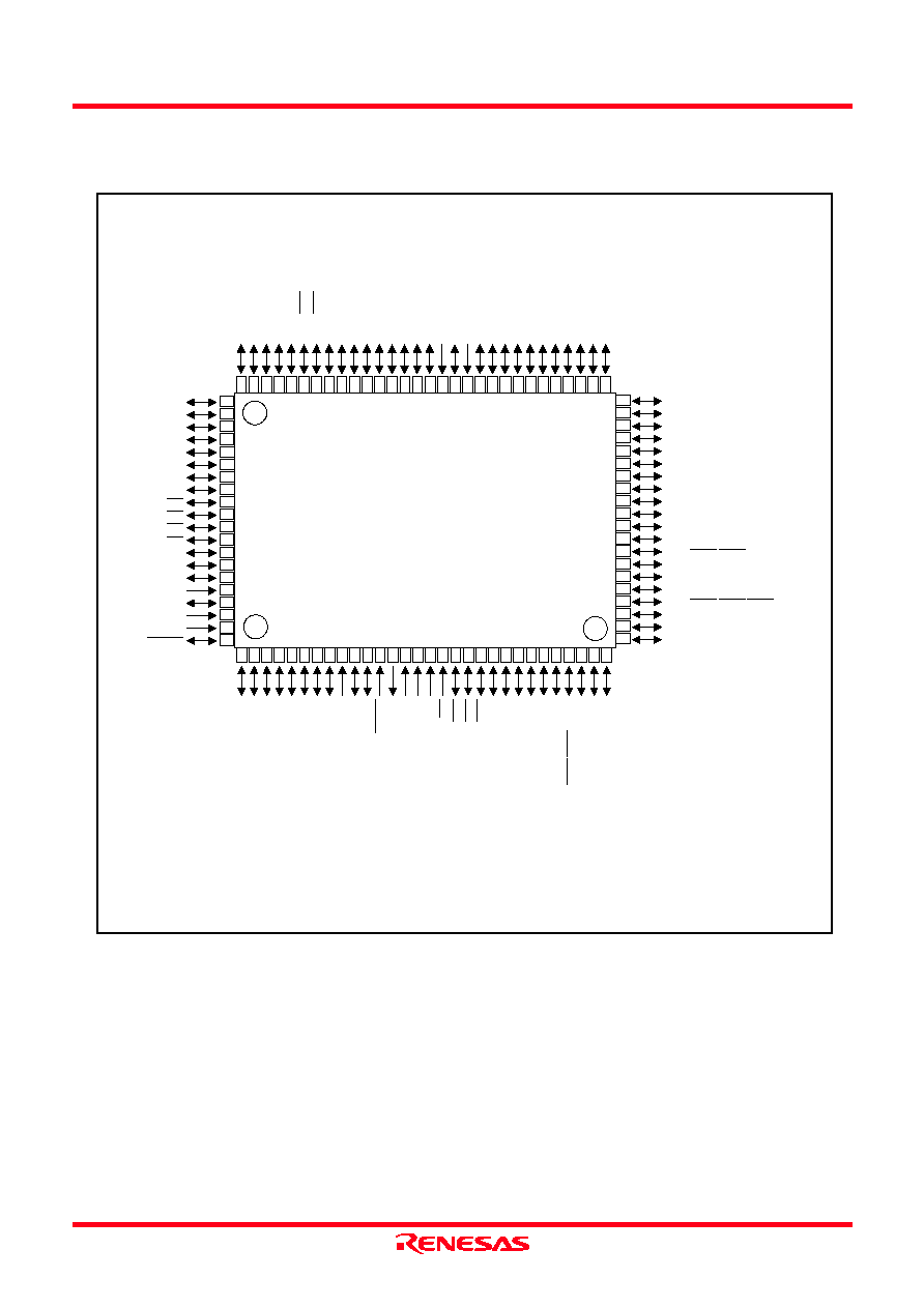
1.5
Pin Configuration
Figures 1.3 to 1.4 show the pin configurations (top view).
Figure 1.3
Pin Configuration (Top View)
1 2 3 4 5 6 7 8 9 10 11 12 13 14 15 16 17 18 19 20 21 22 23 24 25 26 27 28 29 30
31
32
33
34
35
36
37
38
39
40
41
42
43
44
45
46
47
48
49
50
51
52
53
54
55
56
57
58
59
60
61
62
63
64
65
66
67
68
69
70
71
72
73
74
75
76
77
78
79
80
81
82
83
84
85
86
87
88
89
90
91
92
93
94
95
96
97
98
99
100
P0_0/AN0_0
P0_1/AN0_1
P0_2/AN0_2
P0_3/AN0_3
P0_4/AN0_4
P0_5/AN0_5
P0_6/AN0_6
P0_7/AN0_7
P1
_
0
P
1_1
P
1_2
P1
_
3
P1
_
4
VREF
AVSS
VC
C
1
XI
N
XO
UT
VS
S
RESET
CN
VS
S
P8
_
7
/
X
C
I
N
P
8
_6
/
X
COUT
BYTE
P
3_0
P
3_1
P3
_
2
P
3_3
P
3_4
P3
_
5
P
3_6
P
3_7
P4
_
0
P4
_
1
P
4_2
P4
_
3
P7
_
4
/
T
A
2
O
U
T
P7_
6
P5_6
P7_
7
P5_5
P5_4
P5_3
P5_2
VCC2
VSS
P5_7/CLKOUT
P4_5
P4_6
P4_7
AVCC
P6_3/TXD0/SDA0
P6_5/CLK1
P6_6/RXD1/SCL1
P6_7/TXD1/SDA1
P6_1/CLK0
P6_2/RXD0/SCL0
P10_0/AN0
P10_1/AN1
P10_2/AN2
P10_3/AN3
P9_
3
P9_
4
P
9_5
/
A
N
E
X
0
P
9_6
/
A
N
E
X
1
P
9
_
1
/T
B
1
IN
P
9
_
2
/T
B
2
IN
P8_
0
P6_0/CTS0/RTS0
P6_4/CTS1/RTS1/CTS0/CLKS1
P7_
2
/
C
LK
2/
T
A
1
O
UT
P
8
_
2
/IN
T
0
P7
_1
/
R
X
D
2
/
S
C
L2
/
T
A0
I
N
(1
)
P
8
_
3
/IN
T
1
P8
_
5
/
N
MI
P9_7/ADTRG
P4_4
P5_0
P5_1
P
9
_
0
/T
B
0
IN
P7_
0
/
T
XD2
/
S
D
A
2
/
T
A
0
OU
T
(1
)
P
8
_
4
/IN
T
2
P8_
1
P
7
_
3
/C
T
S
2
/
R
T
S
2
/T
A
1
IN
P
7
_
5
/T
A
2
IN
P
1_5/
I
N
T3
P
1_6/
I
N
T4
P1_7
P10_7/AN7/KI3
P10_6/AN6/KI2
P10_5/AN5/KI1
P10_4/AN4/KI0
P2
_
0
P2
_
1
P2
_
2
P2
_
3
P2
_
4
P2
_
5
P2
_
6
P2
_
7
M16C/30P Group
Package : 100P6S-A
PIN CONFIGURATION (top view)
NOTES:
1. P7_0 and P7_1 are N channel open-drain output pins.
2. Use the M16C/30P on VCC1=VCC2.