Regarding the change of names mentioned in the document, such as Mitsubishi
Electric and Mitsubishi XX, to Renesas Technology Corp.
The semiconductor operations of Hitachi and Mitsubishi Electric were transferred to Renesas
Technology Corporation on April 1st 2003. These operations include microcomputer, logic, analog
and discrete devices, and memory chips other than DRAMs (flash memory, SRAMs etc.)
Accordingly, although Mitsubishi Electric, Mitsubishi Electric Corporation, Mitsubishi
Semiconductors, and other Mitsubishi brand names are mentioned in the document, these names
have in fact all been changed to Renesas Technology Corp. Thank you for your understanding.
Except for our corporate trademark, logo and corporate statement, no changes whatsoever have been
made to the contents of the document, and these changes do not constitute any alteration to the
contents of the document itself.
Note : Mitsubishi Electric will continue the business operations of high frequency & optical devices
and power devices.
Renesas Technology Corp.
Customer Support Dept.
April 1, 2003
To all our customers

1
Mitsubishi microcomputers
M16C / 62T Group
SINGLE-CHIP 16-BIT CMOS MICROCOMPUTER
Description
------Table of Contents------
Description
The M16C/62T group of single-chip microcomputers are built using the high-performance silicon gate
CMOS process using a M16C/60 Series CPU core and are packaged in a 100-pin or a 80-pin plastic
molded QFP. These single-chip microcomputers operate using sophisticated instructions featuring a high
level of instruction efficiency. With 1M bytes of address space, they are capable of executing instructions at
high speed. They also feature a built-in multiplier and DMAC, making them ideal for controlling office,
communications, industrial equipment, and other high-speed processing applications.
The M16C/62T group includes a wide range of products with different internal memory types and sizes and
various package types.
Features
∑ Memory capacity .................................. M30623M4T-XXXGP : ROM 32K bytes, RAM 3K bytes
M30622M8T/M8V-XXXFP,M30623M8T/M8V-XXXGP : ROM 64K bytes, RAM 4K bytes
M30622MCT/MCV-XXXFP,M30623MCT/MCV-XXXGP : ROM 128K bytes, RAM 5K bytes
M30622ECT/ECV-XXXFP,M30623ECT/ECV-XXXGP : PROM 128K bytes, RAM 5K bytes
∑ Shortest instruction execution time ......62.5ns (f(X
IN
)=16MH
Z
, V
CC
=5V)
∑ Supply voltage ..................................... Mask ROM version : 4.2 to 5.5V (f(X
IN
)=16MH
Z
, without software wait)
One-time PROM version : 4.5 to 5.5V (f(X
IN
)=16MH
Z
, without software wait)
∑ Low power consumption ......................140mW (V
CC
= 5V, f(X
IN
)=16MH
Z
)
∑ Interrupts
25 internal interrupt sources, 8 external interrupt sources (M30622(100-pin package))
/5 sources (M30623(80-pin package)), 4 software interrupt sources,
7 levels (including key input interrupt)
∑ Multifunction 16-bit timer ......................5 I/O timers + 6 input timers(M30622(100-pin package))
3 I/O timers + 5 input timers(M30623(80-pin package))
∑ Inside 16-bit timer ................................ 3 timers(only M30623(80-pin package))(Note 1)
∑ Serial I/O .............................................. ∑ M30622(100-pin package) : 3 for UART or clock synchronous + 2 for synchronous
∑ M30623(80-pin package) : 3 for UART or clock synchronous(one of exclusive UART)
+ 2 for synchronous(one of exclusive transmission)
∑ DMAC .................................................. 2 channels (trigger: 24 sources)
∑ A-D converter ....................................... 10 bits X 8 channels (Expandable up to 26 channels)
∑ D-A converter ....................................... 8 bits X 2 channels
∑ CRC calculation circuit ......................... 1 circuit
∑ Watchdog timer .................................... 1 line
∑ Programmable I/O ...............................87 lines(M30622(100-pin package)),70 lines(M30623(80-pin package))
∑ Input port ..............................................
_______
1 line (P8
5
shared with NMI pin)
∑ Memory expansion .............................. Available (to 1.2M bytes or 4M bytes)
∑ Chip select output ................................ 4 lines(only M30622(100-pin package))(Note 2)
∑ Clock generating circuit ....................... 2 built-in clock generation circuits (built-in feedback resistor, and external ceramic or quartz oscillator)
Note 1: In M30623(80-pin package), these timers have no corresponding external pin can be used as
internal timers.
Note 2: M30623(80-pin package) has no external pin for chip select output.
Applications
Audio, cameras, office equipment, communications
equipment, portable equipment, cars, etc
Central Processing Unit (CPU) ..................... 12
Reset ............................................................. 15
Processor Mode ............................................ 28
Clock Generating Circuit ............................... 40
Protection ...................................................... 49
Interrupts ....................................................... 50
Watchdog Timer ............................................ 70
DMAC ........................................................... 72
Specifications written in this manual are believed to be accurate, but are
not guaranteed to be entirely free of error.
Specifications in this manual may be changed for functional or performance
improvements. Please make sure your manual is the latest edition.
Timer ............................................................. 82
Timers' function for three-phase motor control.......... 100
Serial I/O ..................................................... 112
A-D Converter ............................................. 148
D-A Converter ............................................. 159
CRC Calculation Circuit .............................. 161
Programmable I/O Ports ............................. 163
Electrical characteristics ............................. 178
Mitsubishi microcomputers
M16C / 62T Group
SINGLE-CHIP 16-BIT CMOS MICROCOMPUTER
4
Description
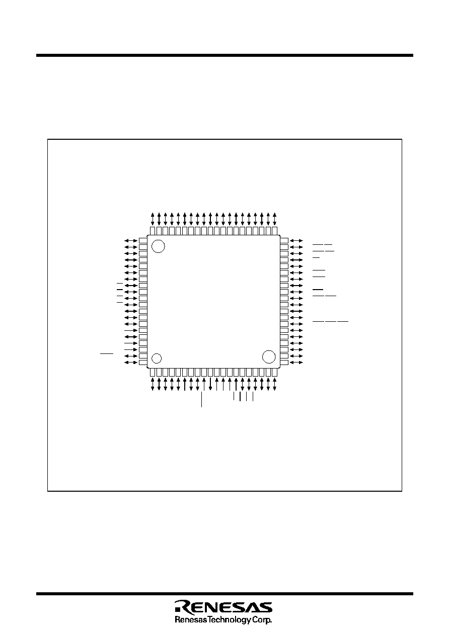
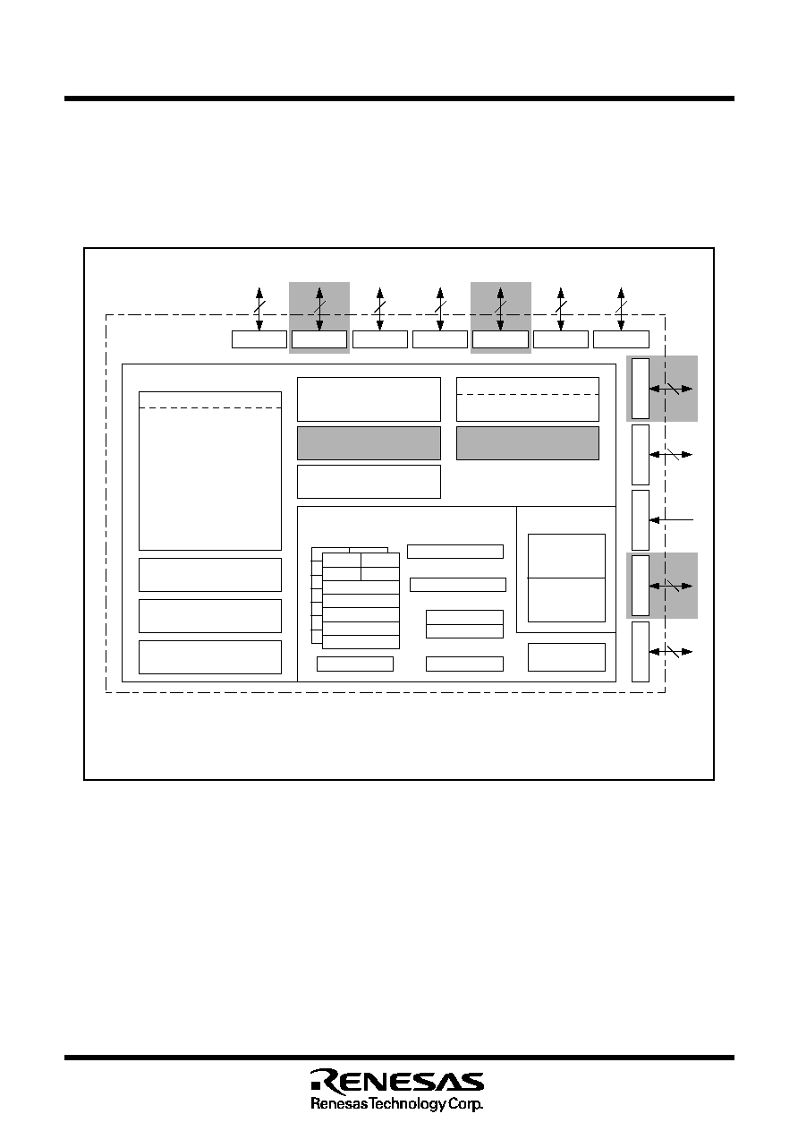
Block Diagram
Figure 1.1.3 is block diagrams of M30622(100-pin package) and 1.1.4 is block diagrams of M30623(80-pin
package).
I/O ports
Port P0
8
Port P1
8
Port P2
8
Port P3
8
Port P4
8
Port P5
8
Port P6
8
Port P7
8
Port P8
7
Port P8
5
Port P9
8
Port P10
8
Internal peripheral functions
Timer
Timer TA0 (16 bits)
Timer TA1 (16 bits)
Timer TA2 (16 bits)
Timer TA3 (16 bits)
Timer TA4 (16 bits)
Timer TB0 (16 bits)
Timer TB1 (16 bits)
Timer TB2 (16 bits)
Timer TB3 (16 bits)
Timer TB4 (16 bits)
Timer TB5 (16 bits)
Watchdog timer
(15 bits)
DMAC
(2 channels)
D-A converter
(8 bits
!
2 channels)
SB
Registers
Program conter
R0H
R0L
R1H
R1L
R2
R3
A0
A1
FB
PC
Sutack pointer
ISP
USP
Vector table
INTB
FLG
M16C/60series 16-bit CPU core
Memory
Multiplier
A-D converter
(10 bits
!
8 channels
Expandable up to 26 channels)
UART/clock synchronous SI/O
(8 bits
!
3 channels) (Note 1)
CRC arithmetic circuit (CCITT)
(Polynominal: X
16
+X
12
+X
5
+1)
System clock generator
X
IN
-X
OUT
X
CIN
-X
COUT
Clock synchronous SI/O
(8 bits
!
2 channels)
ROM
(Note 2)
RAM
(Note 3)
R0H
R0L
R1H
R1L
R2
R3
A0
A1
FB
Note 1: One of 3 channels also functions as IIC bus interface.
Note 2: ROM size depends on MCU type.
Note 3: RAM size depends on MCU type.
Figure 1.1.3. Block diagram of M30622 (100-pin package)