
Rev.1.10 2003.05.28 page 1 of 61
M16C/62 Group (M16C/62P)
SINGLE-CHIP 16-BIT CMOS MICROCOMPUTER
REJ03B0001-0110Z
Rev.1.10
2003.05.28
Overview
The M16C/62 group (M16C/62P) of single-chip microcomputers are built using the high-performance sili-
con gate CMOS process using a M16C/60 Series CPU core and are packaged in a 100-pin and 128-pin
plastic molded QFP. These single-chip microcomputers operate using sophisticated instructions featuring
a high level of instruction efficiency. With 1M bytes of address space, they are capable of executing instruc-
tions at high speed. In addition, this microcomputer contains a multiplier and DMAC which combined with
fast instruction processing capability, makes it suitable for control of various OA, communication, and in-
dustrial equipment which requires high-speed arithmetic/logic operations.
Applications
Audio, cameras, office/communications/portable/industrial equipment, etc
Specifications written in this manual are believed to be accurate, but are
not guaranteed to be entirely free of error. Specifications in this manual
may be changed for functional or performance improvements. Please make
sure your manual is the latest edition.
Overview
Rev.1.10 2003.05.28 page 2 of 61
M16C/62 Group (M16C/62P)
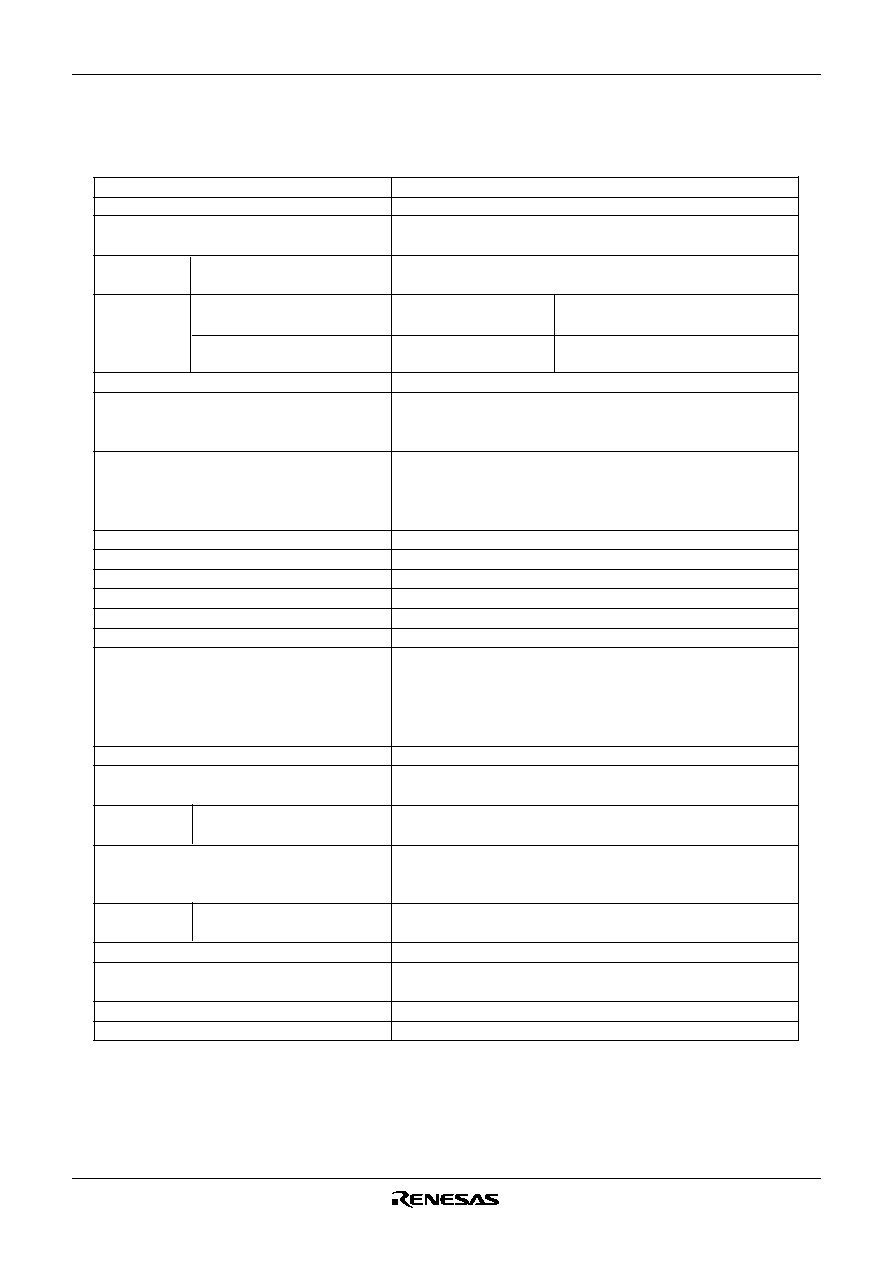
Table 1.1.1. Performance outline of M16C/62P group
Performance Outline
Table 1.1.1 lists performance outline of M16C/62P group.
Item
Performance
Number of basic instructions
91 instructions
Shortest instruction execution time
41.7 ns (f(BCLK)= 24MH
Z
, V
CC1
= 3.0V to 5.5V)
100 ns (f(BCLK)= 10MH
Z
, V
CC1
= 2.7V to 5.5V)
Memory
ROM
(See the product list)
capacity
RAM
(See the product list)
I/O port
100-pin version
8 bits x 10, 7 bits x 1
P0 to P5: V
CC2
ports
P0 to P10 (except P8
5
)
P6 to P10: V
CC1
ports
128-pin version
8 bits x 13, 7 bits x 1,
P0 to P5, P12, P13: V
CC2
ports
P0 to P14 (except P8
5
)
2 bits x 1
P6 to P10, P11, P14: V
CC1
ports
Input port
P8
5
_______
1 bit x 1 (NMI pin level judgment): V
CC1
ports
Multifunction timer
Output
16 bits x 5 channels (TA0, TA1, TA2, TA3, TA4)
Input
16 bits x 6 channels (TB0, TB1, TB2, TB3, TB4, TB5)
Serial I/O
3 channels (UART0, UART1, UART2)
UART, clock synchronous, I
2
C bus
1
(option
4
), or IEBus
2
(option4)
2 channels (SI/O3, SI/O4)
Clock synchronous
A-D converter
10 bits x (8 x 3 + 2) channels
D-A converter
8 bits x 2
DMAC
2 channels (trigger: 25 sources)
CRC calculation circuit
CRC-CCITT
Watchdog timer
15 bits x 1 (with prescaler)
Interrupt
29 internal and 8 external sources, 4 software sources, 7 levels
Clock generation circuit
4 circuits
∑ Main clock
∑ Sub-clock
∑ Ring oscillator(main-clock oscillation stop detect function)
∑ PLL frequency synthesizer
Voltage detection circuit
Present (option
4
)
Power supply voltage
V
CC1
=3.0V to 5.5V, V
CC2
=3.0V to V
CC1
(f(BCLK)=24MH
Z
)
V
CC1
=V
CC2
=2.7V to 5.5V (f(BCLK)=10MH
Z
)
Flash memory Program/erase voltage
3.3V
±
0.3V or 5.0V
±
0.5V
Number of program/erase
100 times, 10000 times
3
(option
4
)
Power consumption
14mA (V
CC1
=V
CC2
=5V, f(BCLK)=24MH
Z
)
8mA (V
CC1
=V
CC2
=3V, f(BCLK)=10MH
Z
)
1.8
µ
A (V
CC1
=V
CC2
=3V, f(X
CIN
)=32kH
Z
, when wait mode)
I/O
I/O withstand voltage
5.0V
characteristics Output current
5mA
Memory expansion
Available (to 4M bytes)
Operating ambient temperature
-20 to 85
∞
C
-40 to 85
∞
C (option
4
)
Device configuration
CMOS high performance silicon gate
Package
100-pin and 128-pin plastic mold QFP
(These circuits contain a built-in feedback
resistor and external ceramic/quartz oscillator)
Notes:
1. I
2
C bus is a registered trademark of Koninklijke Philips Electronics N. V.
2. IEBus is a registered trademark of NEC Electronics Corporation.
3. Block 1 and block A are a 10,000 times of programming and erasure. All other blocks are guaranteed of 1,000 times
of programming and erasure. (Under development; mass production scheduled to start in the 3rd quarter of 2003)
4. If you desire this option, please so specify.

Overview
Rev.1.10 2003.05.28 page 3 of 61
M16C/62 Group (M16C/62P)
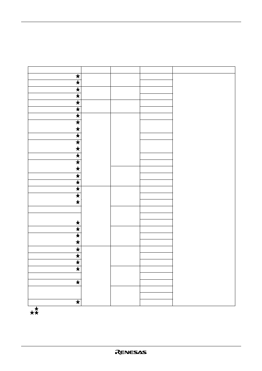
Block Diagram
Figure 1.1.1 is a block diagram of the M16C/62P group.
Timer (16-bit)
Output (timer A): 5
Input (timer B): 6
Internal peripheral functions
Watchdog timer
(15 bits)
DMAC
(2 channels)
D-A converter
(8 bits X 2 channels)
A-D converter
(10 bits
X
8 channels
Expandable up to 26 channels)
UART or
clock synchronous serial I/O
(8 bits
X
3 channels)
System clock generator
X
IN
-X
OUT
X
CIN
-X
COUT
PLL frequency synthesizer
Ring oscillator
M16C/60 series16-bit CPU core
Port P0
8
Port P1
8
Port P2
8
Port P3
8
Port P4
8
Port P5
8
Port P6
8
CRC arithmetic circuit (CCITT )
(Polynomial : X
16
+X
12
+X
5
+1)
Memory
8
7
8
8
Port P10
Port P9
Port P8
Port P7
Port P8
5
ROM
(Note 1)
RAM
(Note 2)
Note 1: ROM size depends on microcomputer type.
Note 2: RAM size depends on microcomputer type.
Note 3: Ports P11 to P14 exist only in 128-pin version.
Clock synchronous serial I/O
(8 bits
X
2 channels)
R0L
R0H
R1H
R1L
R2
R3
SB
FLG
USP
ISP
INTB
PC
Multiplier
Port P11
8
Port P14
2
Port P12
8
Port P13
8
Three-phase motor
control circuit
A0
A1
FB
<V
CC2
ports>
(Note 3)
(Note 3)
(Note 3)
(Note 3)
<V
CC1
ports>
<V
CC1
ports>
<V
CC1
ports>
<V
CC2
ports>
Figure 1.1.1. Block Diagram
Overview
Rev.1.10 2003.05.28 page 4 of 61
M16C/62 Group (M16C/62P)
Product List
Tables 1.1.2 and 1.1.3 list the M16C/62P group products and Figure 1.1.2 shows the type numbers,
memory sizes and packages.
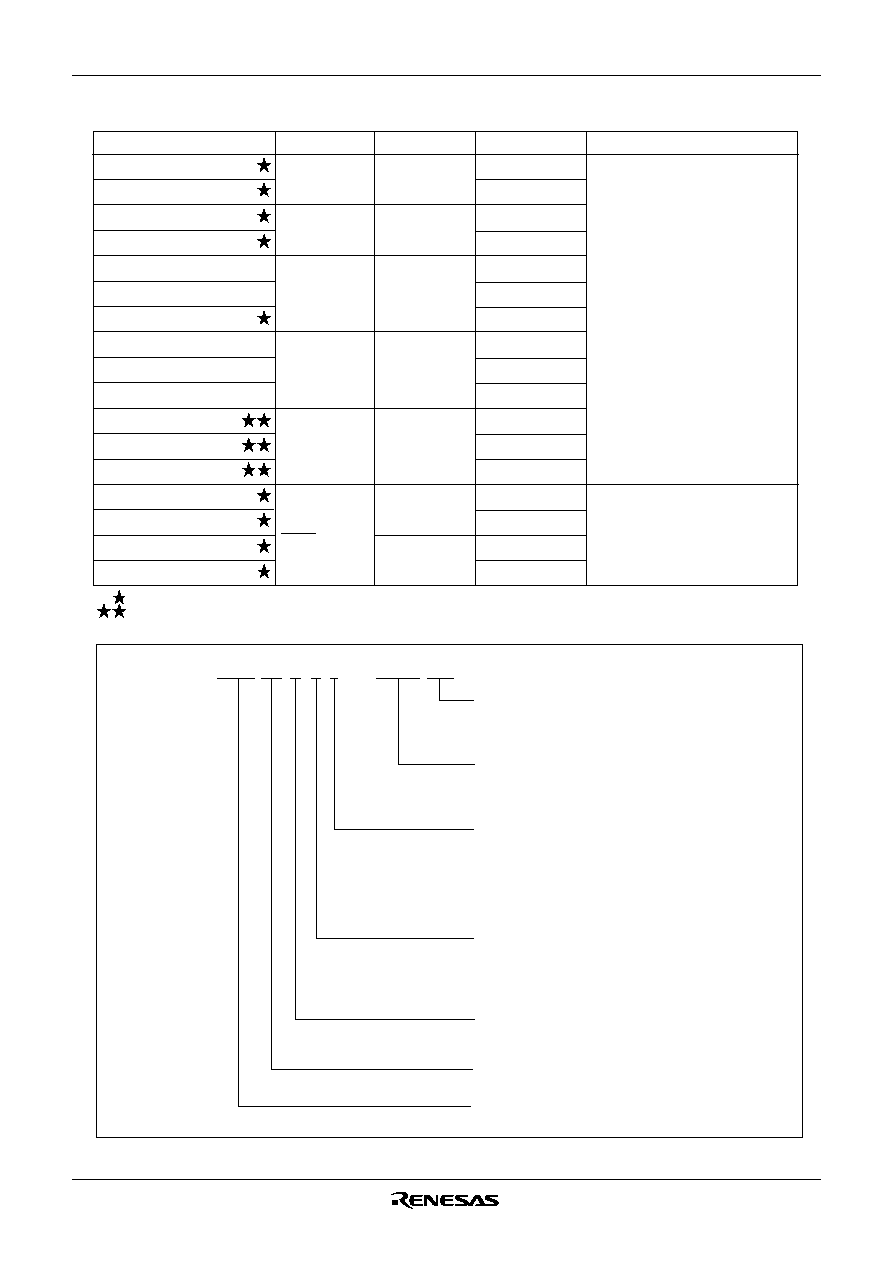
Table 1.1.2. Product List (1)
RAM capacity
ROM capacity
Package type
Remarks
Type No.
As of April 2003
MASK ROM version
384K bytes
M30622MEP-XXXFP
M30620MCP-XXXFP
M30622MAP-XXXFP
M30622M8P-XXXFP
M30622M6P-XXXFP
100P6Q-A
M30622MEP-XXXGP
M30620MCP-XXXGP
M30622MAP-XXXGP
M30622M8P-XXXGP
M30622M6P-XXXGP
100P6S-A
100P6Q-A
100P6S-A
100P6Q-A
100P6S-A
100P6Q-A
100P6S-A
100P6Q-A
100P6S-A
M30623MEP-XXXGP
128P6Q-A
M30624MGP-XXXFP
100P6S-A
M30624MGP-XXXGP
100P6Q-A
M30625MGP-XXXGP
128P6Q-A
M30622MGP-XXXFP
100P6S-A
M30622MGP-XXXGP
100P6Q-A
128P6Q-A
M30623MGP-XXXGP
M30626MWP-XXXFP
100P6S-A
M30626MWP-XXXGP
100P6Q-A
128P6Q-A
M30627MWP-XXXGP
M30624MWP-XXXFP
100P6S-A
100P6Q-A
M30624MWP-XXXGP
128P6Q-A
M30625MWP-XXXGP
M30622MWP-XXXFP
100P6S-A
M30622MWP-XXXGP
100P6Q-A
M30626MHP-XXXFP
100P6S-A
M30626MHP-XXXGP
100P6Q-A
128P6Q-A
M30623MWP-XXXGP
128P6Q-A
M30627MHP-XXXGP
100P6S-A
M30624MHP-XXXFP
100P6Q-A
M30624MHP-XXXGP
128P6Q-A
M30625MHP-XXXGP
M30622MHP-XXXFP
100P6S-A
M30622MHP-XXXGP
100P6Q-A
128P6Q-A
M30623MHP-XXXGP
48K bytes
64K bytes
96K bytes
128K bytes
192K bytes
256K bytes
320K bytes
31K bytes
24K bytes
16K bytes
31K bytes
24K bytes
16K bytes
12K bytes
12K bytes
10K bytes
5K bytes
4K bytes
4K bytes
20K bytes
: Under development
: Under planning
Overview
Rev.1.10 2003.05.28 page 5 of 61
M16C/62 Group (M16C/62P)
Package type:
FP : Package
100P6S-A
GP : Package
100P6Q-A, 128P6Q-A
ROM No.
Omitted for flash memory version and
external ROM version
ROM capacity:
6: 48K bytes
8: 64K bytes
A: 96K bytes
C: 128K bytes
E: 192K bytes
Memory type:
M: Mask ROM version
F: Flash memory version
S: External ROM version
Type No. M 3 0 6 2 6 M H P≠ X X X F P
M16C/62 Group
M16C Family
Shows RAM capacity, pin count, etc
(The value itself has no specific meaning)
G: 256K bytes
W: 320K bytes
H: 384K bytes
J: 512K bytes
Figure 1.1.2. Type No., Memory Size, and Package
M30627FJPGP
M30625FGPGP
128P6Q-A
100P6S-A
M30622F8PFP
M30622F8PGP
100P6Q-A
M30620FCPFP
100P6S-A
100P6Q-A
M30620FCPGP
M30624FGPGP
100P6S-A
M30624FGPFP
M30626FHPFP
128P6Q-A
100P6S-A
100P6Q-A
M30626FHPGP
M30627FHPGP
M30626FJPFP
100P6Q-A
100P6S-A
M30626FJPGP
M30620SPFP
M30620SPGP
100P6Q-A
M30622SPFP
M30622SPGP
128P6Q-A
100P6Q-A
100P6S-A
100P6Q-A
100P6S-A
384K bytes
64K bytes
128K bytes
256K bytes
512K bytes
RAM capacity
ROM capacity
Package type
Remarks
Type No.
Flash memory version
External ROM version
31K bytes
10K bytes
4K bytes
20K bytes
4K bytes
31K bytes
10K bytes
: Under development
: Under planning
As of April 2003
Table 1.1.3. Product List (2)