Regarding the change of names mentioned in the document, such as Mitsubishi
Electric and Mitsubishi XX, to Renesas Technology Corp.
The semiconductor operations of Hitachi and Mitsubishi Electric were transferred to Renesas
Technology Corporation on April 1st 2003. These operations include microcomputer, logic, analog
and discrete devices, and memory chips other than DRAMs (flash memory, SRAMs etc.)
Accordingly, although Mitsubishi Electric, Mitsubishi Electric Corporation, Mitsubishi
Semiconductors, and other Mitsubishi brand names are mentioned in the document, these names
have in fact all been changed to Renesas Technology Corp. Thank you for your understanding.
Except for our corporate trademark, logo and corporate statement, no changes whatsoever have been
made to the contents of the document, and these changes do not constitute any alteration to the
contents of the document itself.
Note : Mitsubishi Electric will continue the business operations of high frequency & optical devices
and power devices.
Renesas Technology Corp.
Customer Support Dept.
April 1, 2003
To all our customers

Mitsubishi microcomputers
M16C / 6N0 / 6N1 Group
SINGLE-CHIP 16-BIT CMOS MICROCOMPUTER
1
Description
------Table of Contents------
Description
The M16C/6N group of single-chip microcomputers are built using the high-performance silicon gate
CMOS process using a M16C/60 series CPU core and are packaged in a 100-pin plastic molded QFP.
These single-chip microcomputers operate using sophisticated instructions featuring a high level of instruc-
tion efficiency. With 1M bytes of address space, they are capable of executing instructions at high speed.
They also feature a built-in multiplier and DMAC, making them ideal for controlling office, communications,
industrial equipment, and other high-speed processing applications.
The M16C/6N group is consisted of two sub-groups, M16C/6N0 group and M16C/6N1 group. The M16C/
6N0 group has two CAN (Controller Area Network) modules and the M16C/6N1 group has one CAN mod-
ule (See Figure 1.1.4 Memory Expansion). The CAN modules comply with the 2.0B specification. The
M16C/6N group is suited to drive automotive and industrial control systems.
Features
∑ Memory capacity .................................. ROM 128K/256K bytes
RAM 5K/10K bytes
∑ Shortest instruction execution time ...... 62.5 ns (f(X
IN
) = 16MHz, 1/1 prescaler, without software wait)
∑ Supply voltage ..................................... 4.2 to 5.5V (f(X
IN
) = 16MHz, 1/1 prescaler, without software wait)
∑ Low power dissipation ......................... 60mA M16C/6N0 group Mask products
65mA M16C/6N0 group Flash products
50mA M16C/6N1 group Mask products
55mA M16C/6N1 group Flash products
(f(X
IN
) = 16MHz, 1/1 prescaler, without software wait)
∑ Interrupts .............................................. 29 internal and 9 external interrupt sources, 4 software
interrupt sources, 7 priority levels (including key input interrupt)
∑ Multifunction 16-bit timer ...................... 5 output timers + 6 input timers
∑ Serial I/O .............................................. 3 channels (UART/clock synchronous, 1 channel clock synchronous)
∑ DMAC .................................................. 2 channels (trigger: 24 sources)
∑ CAN module ........................................ 2 channels for M16C/6N0 group
1 channel for M16C/6N1 group
∑ A-D converter ....................................... 10 bits X (8X3+2) channels
∑ D-A converter ....................................... 8 bits X 2 channels
∑ CRC calculation circuit ......................... 1 circuit
∑ Watchdog timer .................................... 1 15-bit timer
∑ Programmable I/O ............................... 87 lines
∑ Input port ..............................................
______
1 line (P8
5
shared with NMI pin)
∑ Chip select output ................................ 4 lines
∑ Memory expansion .............................. Available (to a maximum of 1M bytes)
∑ Clock generating circuit ....................... 3 built-in circuits
Main clock generating circuit, Sub clock generating circuit,
(built-in feedback resistor, and external ceramic or quartz crystal oscillator)
Ring oscillation circuit (with an oscillation stop detection circuit)
Applications
Automotive and industrial control systems
Central Processing Unit (CPU) ..................... 11
Reset ............................................................. 14
Processor Mode ............................................ 22
Clock Generating Circuit ............................... 36
Protection ...................................................... 52
Interrupt ......................................................... 53
Watchdog Timer ............................................ 75
DMAC ........................................................... 77
Timer ............................................................. 87
Serial I/O ..................................................... 117
A-D Converter ............................................. 157
D-A Converter ............................................. 167
CRC Calculation Circuit .............................. 169
CAN Module ................................................ 171
Programmable I/O Port ............................... 196
Electrical Characteristics ............................. 207
Flash Memory Version ................................ 224
Specifications written in this
manual are believed to be ac-
curate, but are not guaranteed
to be entirely free of error.
Specifications in this manual
may be changed for functional
or performance improvements.
Please make sure your manual
is the latest edition.
Mitsubishi microcomputers
M16C / 6N0 / 6N1 Group
SINGLE-CHIP 16-BIT CMOS MICROCOMPUTER
2
Description
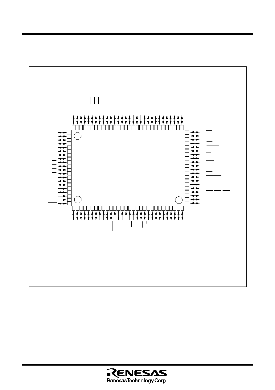
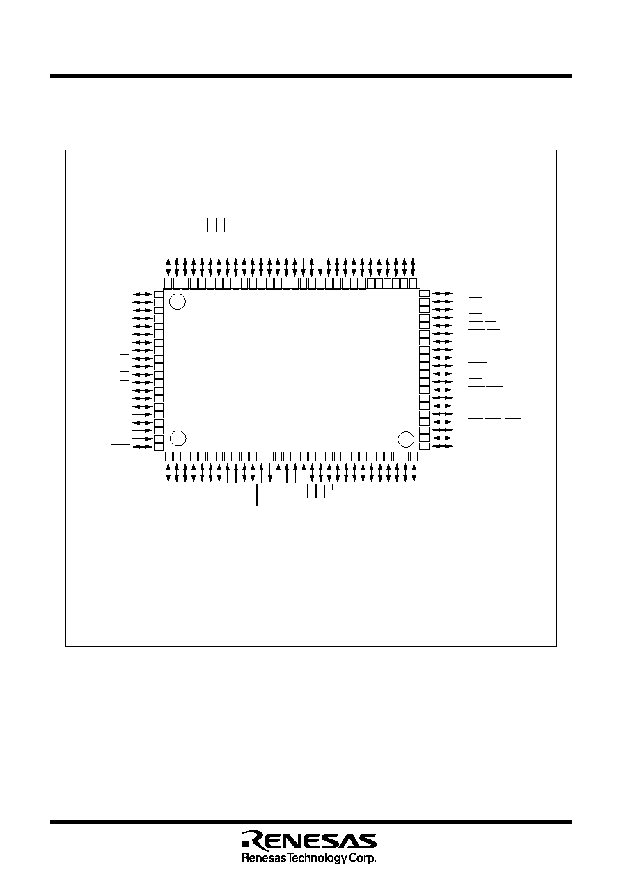
Pin configuration (top view)
Package: 100P6S-A
Figure 1.1.1. Pin configuration for M16C/6N0 group (top view)
Pin Configuration
Figures 1.1.1 and 1.1.2 show the pin configuration (top view).
1
2 3
4 5
6
7
8
9 10 11 12 13 14 15 16 17 18 19 20 21 22 23 24 25 26 27 28 29 30
31
32
33
34
35
36
37
38
39
40
41
42
43
44
45
46
47
48
49
50
51
52
53
54
55
56
57
58
59
60
61
62
63
64
65
66
67
68
69
70
71
72
73
74
75
76
77
78
79
80
81
82
83
84
85
86
87
88
89
90
91
92
93
94
95
96
97
98
99
100
P0
7
/AN
07
/D
7
P1
0
/D
8
P1
1
/D
9
P1
2
/D
10
P1
3
/D
11
P1
4
/D
12
V
REF
AV
SS
V
CC
X
IN
X
OUT
V
SS
RESET
CNVss
P8
7
/X
CIN
P8
6
/X
COUT
BYTE
P3
0
/A
8
(/-/D
7
)
P3
1
/A
9
P3
2
/A
10
P3
3
/A
11
P3
4
/A
12
P3
5
/A
13
P3
6
/A
14
P3
7
/A
15
P4
0
/A
16
P4
1
/A
17
P4
2
/A
18
P4
3
/A
19
P7
4
/TA2
OUT
/W
P5
6
/ALE
P5
5
/HOLD
P5
4
/HLDA
P5
3
/BCLK
P5
2
/RD
Vcc
Vss
P5
7
/RDY/CLK
OUT
P4
5
/CS1
P4
6
/CS2
P4
7
/CS3
AVcc
P6
3
/T
X
D
0
P6
5
/CLK
1
P6
6
/RxD
1
P6
7
/T
X
D
1
P6
1
/CLK
0
P6
2
/RxD
0
P10
0
/AN
0
P10
1
/AN
1
P10
2
/AN
2
P10
3
/AN
3
P9
3
/DA
0
/TB3
IN
P9
4
/DA
1
/TB4
IN
P9
6
/ANEX1/CT
X
0
P9
1
/TB1
IN
/S
IN
3(Note)
P9
2
/TB2
IN
/S
OUT
3
P8
0
/TA4
OUT
/U
P6
0
/CTS
0
/RTS
0
P6
4
/CTS
1
/RTS
1
/CTS
0
/CLKS
1
P7
2
/CLK
2
/TA1
OUT
/V
P8
2
/INT
0
P7
1
/RxD
2
/SCL/TA0
IN
/TB5
IN
(Note)
P8
3
/INT
1
P8
5
/NMI
P9
7
/AD
TRG
P4
4
/CS0
P5
0
/WRL/WR
P5
1
/WRH/BHE
P9
0
/TB0
IN
/CLK3
P7
0
/T
X
D
2
/SDA/TA0
OUT
P8
4
/INT
2
P8
1
/TA4
IN
/U
P7
5
/TA2
IN
/W
P1
5
/D
13
/INT3
P1
6
/D
14
/INT4
P1
7
/D
15
/INT5
P10
7
/AN
7
/KI
3
P10
6
/AN
6
/KI
2
P10
5
/AN
5
/KI
1
P10
4
/AN
4/
KI
0
M16C/6N0 Group
P7
3
/CTS
2
/RTS
2
/TA1
IN
/V
P0
6
/AN
06
/D
6
P0
5
/AN
05
/D
5
P0
4
/AN
04
/D
4
P0
3
/AN
03
/D
3
P0
2
/AN
02
/D
2
P0
1
/AN
01
/D
1
P0
0
/AN
00
/D
0
P2
0
/AN
20
/A
0
/(D
0
/-)
P2
1
/AN
21
/A
1
/(D
1
/D
0
)
P2
2
/AN
22
/A
2
/(D
2
/D
1
)
P2
3
/AN
23
/A
3
/(D
3
/D
2
)
P2
4
/AN
24
/A
4
/(D
4
/D
3
)
P2
5
/AN
25
/A
5
/(D
5
/D
4
)
P2
6
/AN
26
/A
6
/(D
6
/D
5
)
P2
7
/AN
27
/A
7
/(D
7
/D
6
)
P9
5
/ANEX0/CR
X
0
P7
7
/TA3
IN
/CR
X
1
P7
6
/TA3
OUT
/CT
X
1
Note: P7
1
and P9
1
are N channel open-drain output pin.
Mitsubishi microcomputers
M16C / 6N0 / 6N1 Group
SINGLE-CHIP 16-BIT CMOS MICROCOMPUTER
4
Description
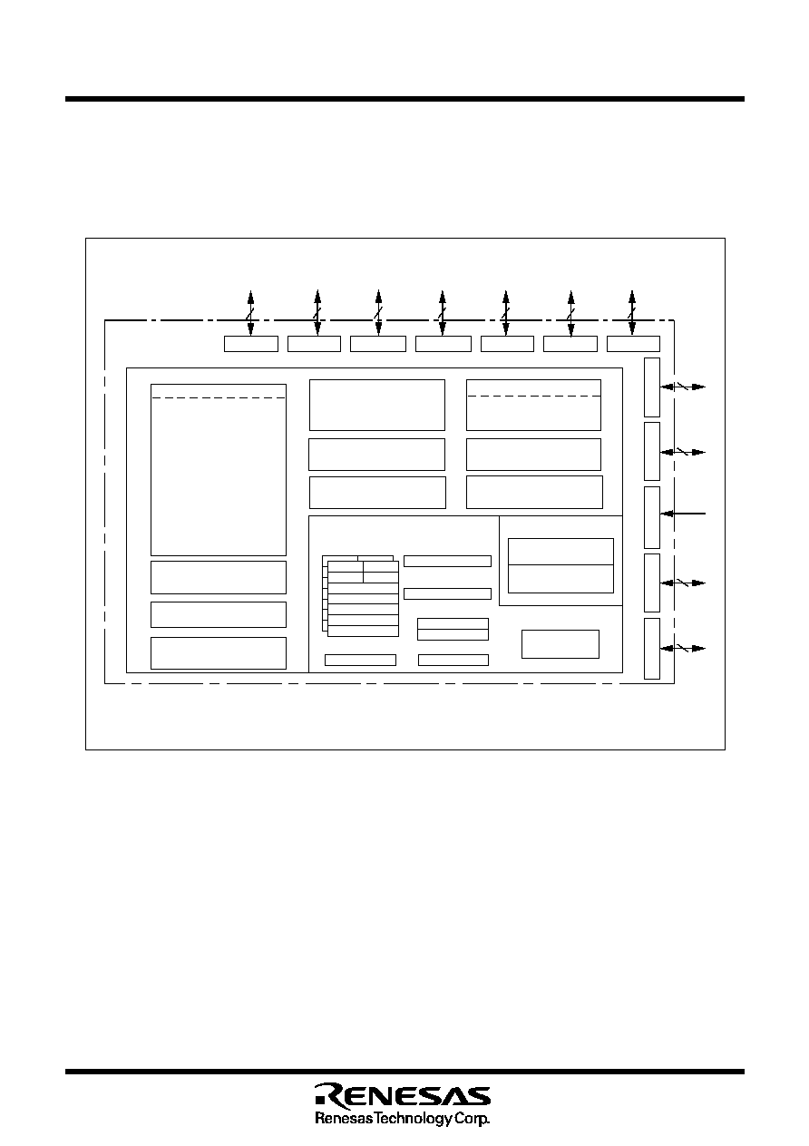
Block Diagram
Figure 1.1.3 is a block diagram of the M16C/6N group.
Block diagram of the M16C/6N group
Figure 1.1.3. Block diagram of M16C/6N group
Note 1: Memory sizes depend on MCU type.
Note 2: Number of channels depends on sub-group.
Timer
Timer TA0 (16 bits)
Timer TA1 (16 bits)
Timer TA2 (16 bits)
Timer TA3 (16 bits)
Timer TA4 (16 bits)
Timer TB0 (16 bits)
Timer TB1 (16 bits)
Timer TB2 (16 bits)
Internal peripheral functions
Watchdog timer
(15 bits)
DMAC
(2 channels)
A-D converter
(10 bits
X
(8
X
3+2) channels)
UART/clock synchronous SI/O
(8 bits
X
3 channels)
X
IN
-
X
OUT
Ring oscillator
X
CIN
-
X
COUT
System clock generator
M16C/60 series16-bit CPU core
I/O ports
Port P0
8
Port P1
8
Port P2
8
Port P3
8
Port P4
8
Port P5
8
Port P6
8
8
R0L
R0H
R1H
R1L
R2
R3
A0
A1
FB
R0L
R0H
R1H
R1L
R2
R3
A0
A1
FB
Registers
ISP
USP
Stack pointer
Flag register
Vector table
INTB
CAN module
(1 or 2 channels)
(Note 2)
Multiplier
7
8
8
Port P10
Port P9
Port P8
Port P7
Memory
Port P8
5
ROM
(Note 1)
(Note 1)
RAM
SB
FLG
PC
Program counter
Clock synchronous SI/O
(8 bits
X
1 channel)
D-A converter
(8 bits x 2 channels)
Timer TB3 (16 bits)
Timer TB4 (16 bits)
Timer TB5 (16 bits)
CRC arithmetic circuit (CCITT)
(Polynomial : X
16
+X
12
+X
5
+1)