ChipFind - документация

Электронный компонент: M30800FCHTFP

Скачать:  PDF   ZIP

Document Outline

Regarding the change of names mentioned in the document, such as Mitsubishi
Electric and Mitsubishi XX, to Renesas Technology Corp.
The semiconductor operations of Hitachi and Mitsubishi Electric were transferred to Renesas
Technology Corporation on April 1st 2003. These operations include microcomputer, logic, analog
and discrete devices, and memory chips other than DRAMs (flash memory, SRAMs etc.)
Accordingly, although Mitsubishi Electric, Mitsubishi Electric Corporation, Mitsubishi
Semiconductors, and other Mitsubishi brand names are mentioned in the document, these names
have in fact all been changed to Renesas Technology Corp. Thank you for your understanding.
Except for our corporate trademark, logo and corporate statement, no changes whatsoever have been
made to the contents of the document, and these changes do not constitute any alteration to the
contents of the document itself.
Note : Mitsubishi Electric will continue the business operations of high frequency & optical devices
and power devices.
Renesas Technology Corp.
Customer Support Dept.
April 1, 2003
To all our customers
1
Under
development
Preliminary Specifications REV.D
Specifications in this manual are tentative and subject to change.
Mitsubishi Microcomputers
M16C/80 group
SINGLE-CHIP 16-BIT CMOS MICROCOMPUTER
Description
------Table of Contents------
Description
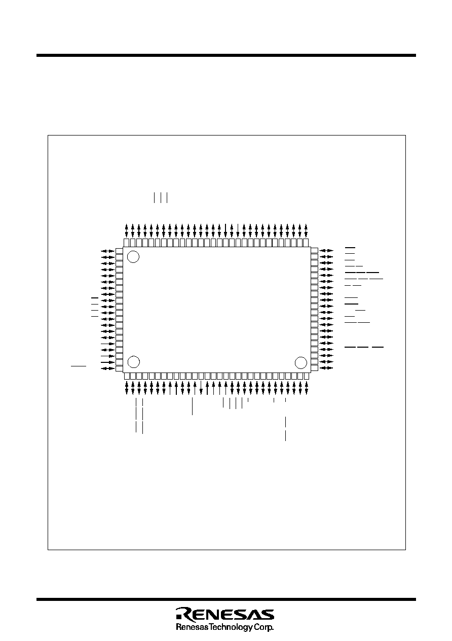
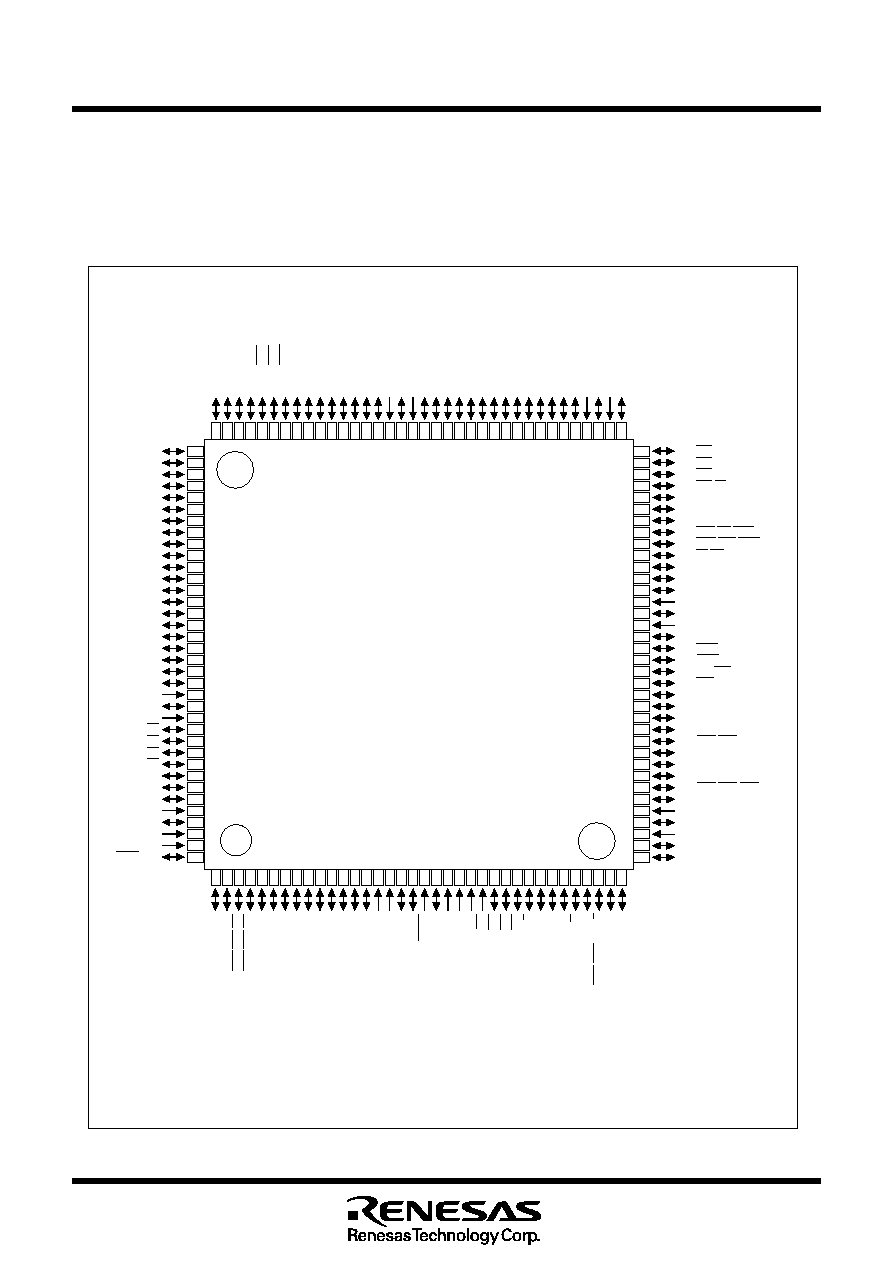
The M16C/80 group of single-chip microcomputers are built using the high-performance silicon gate CMOS
process using a M16C/80 Series CPU core and are packaged in a 100-pin and 144-pin plastic molded
QFP. The peripheral functions of 100-pin and 144-pin are common. These single-chip microcomputers
operate using sophisticated instructions featuring a high level of instruction efficiency. With 16M bytes of
address space, they are capable of executing instructions at high speed. They also feature a built-in multi-
plier and DMAC, making them ideal for controlling office, communications, industrial equipment, and other
high-speed processing applications.
Features
Memory capacity .................................. ROM (See ROM expansion figure.)
RAM 10 to 24 Kbytes
Shortest instruction execution time ...... 50ns (f(X
IN
)=20MHz)
Supply voltage ..................................... 4.2 to 5.5V (f(X
IN
)=20MHz)
Mask ROM, external ROM and flash memory versions
2.7 to 5.5V (f(X
IN
)=10MHz)
Mask ROM, external ROM and flash memory versions
Low power consumption ...................... 45mA (M30800MC-XXXFP)
(f(X
IN
) = 20MHz without software wait,Vcc=5V)
Interrupts .............................................. 29 internal and 8 external interrupt sources, 5 software interrupt
sources; 7 levels (including key input interrupt)
Multifunction 16-bit timer ...................... 5 output timers + 6 input timers
Serial I/O .............................................. 5 channels for UART or clock synchronous
DMAC .................................................. 4 channels (trigger: 31 sources)
DRAMC ................................................ Used for EDO, FP, CAS before RAS refresh, self-refresh
A-D converter ....................................... 10 bits X 8 channels (Expandable up to 10 channels)
D-A converter ....................................... 8 bits X 2 channels
CRC calculation circuit ......................... 1 circuit
X-Y converter ....................................... 1 circuit
Watchdog timer .................................... 1 line
Programmable I/O ............................... 87 lines:100-pin version, 123 lines:144-pin version
Input port ..............................................
_______
1 line (P8
5
shared with NMI pin)
Memory expansion .............................. Available (16M bytes)
Chip select output ................................ 4 lines
Clock generating circuit ....................... 2 built-in clock generation circuits
(built-in feedback resistance, and external ceramic or quartz oscillator)
Applications
Audio, cameras, office equipment, communications equipment, portable equipment, etc.
Specifications written in this manual are believed to be ac-
curate, but are not guaranteed to be entirely free of error.
Specifications in this manual may be changed for func-
tional or performance improvements. Please make sure
your manual is the latest edition.
A-D Converter ............................................. 165
D-A Converter ............................................. 175
CRC Calculation Circuit .............................. 177
X-Y converter .............................................. 179
DRAM controller .......................................... 182
Programmable I/O Ports ............................. 189
Usage Precaution ....................................... 207
Electric characteristics ................................ 219
Flash memory version ................................. 266
CPU .............................................................. 13
Reset ............................................................. 18
Processor Mode ............................................ 26
Clock Generating Circuit ............................... 43
Protection ...................................................... 55
Interrupts ....................................................... 56
Watchdog Timer ............................................ 78
DMAC ........................................................... 80
Timer ............................................................. 91
Serial I/O ..................................................... 123
Under
development
Preliminary Specifications REV.D
Specifications in this manual are tentative and subject to change.
Mitsubishi Microcomputers
M16C/80 group
SINGLE-CHIP 16-BIT CMOS MICROCOMPUTER
2
Description
1
2 3
4 5
6
7
8
9 10 11 12 13 14 15 16 17 18 19 20 21 22 23 24 25 26 27 28 29 30
31
32
33
34
35
36
37
38
39
40
41
42
43
44
45
46
47
48
49
50
51
52
53
54
55
56
57
58
59
60
61
62
63
64
65
66
67
68
69
70
71
72
73
74
75
76
77
78
79
80
81
82
83
84
85
86
87
88
89
90
91
92
93
94
95
96
97
98
99
100
P0
0
/D
0
P0
1
/D
1
P0
2
/D
2
P0
3
/D
3
P0
4
/D
4
P0
5
/D
5
P0
6
/D
6
P0
7
/D
7
P1
0
/D
8
P1
1
/D
9
P1
2
/D
10
P1
3
/D
11
P1
4
/D
12
V
REF
AV
SS
V
CC
X
IN
X
OUT
V
SS
RESET
CNVss
P8
7
/X
CIN
P8
6
/X
COUT
BYTE
P2
0
/A
0
(/D
0
)
P2
1
/A
1
(/D
1
)
P2
2
/A
2
(/D
2
)
P2
3
/A
3
(/D
3
)
P2
4
/A
4
(/D
4
)
P2
5
/A
5
(/D
5
)
P2
6
/A
6
(/D
6
)
P2
7
/A
7
(/D
7
)
P3
0
/A
8
(MA0)(/D
8
)
P3
1
/A
9
(MA1)(/D
9
)
P3
2
/A
10
(MA2)(/D
10
)
P3
3
/A
11
(MA3)(/D
11
)
P3
4
/A
12
(MA4)(/D
12
)
P3
5
/A
13
(MA5)(/D
13
)
P3
6
/A
14
(MA6)(/D
14
)
P3
7
/A
15
(MA7)(/D
15
)
P4
0
/A
16
(MA8)
P4
1
/A
17
(MA9)
P4
2
/A
18
(MA10)
P4
3
/A
19
(MA11)
P7
4
/TA2
OUT
/W
P7
6
/TA3
OUT
P7
7
/TA3
IN
P5
5
/HOLD
P5
4
/HLDA/ALE
P5
3
/BCLK/ALE/CLK
OUT
Vcc
Vss
P5
7
/RDY
P4
5
/CS2/A
21
P4
6
/CS1/A
22
AVcc
P6
3
/T
X
D
0
P6
5
/CLK
1
P6
6
/RxD
1
P6
7
/T
X
D
1
P6
1
/CLK
0
P6
2
/RxD
0
P10
0
/AN
0
P10
1
/AN
1
P10
2
/AN
2
P10
3
/AN
3
P9
5
/ANEX0/CLK
4
P9
6
/ANEX1/T
X
D
4
/SDA
4
/SRxD
4
P9
1
/TB1
IN
/R
X
D
3
/SCL
3
/STxD
3
P9
2
/TB2
IN
/T
X
D
3
/SDA
3
/SRxD
3
P8
0
/TA4
OUT
/U
P6
0
/CTS
0
/RTS
0
P6
4
/CTS
1
/RTS
1
/CTS
0
/CLKS
1
P7
2
/CLK
2
/TA1
OUT
/V
P8
2
/INT
0
P7
1
/RxD
2
/SCL
2
/TA0
IN
/TB5
IN
(Note)
P8
3
/INT
1
P8
5
/NMI
P9
7
/AD
TRG
/R
X
D
4
/SCL
4
/STxD
4
P4
4
/CS3/A
20
(MA12)
P9
0
/TB0
IN
/CLK
3
P7
0
/T
X
D
2
/SDA
2
/TA0
OUT
(Note)
P8
4
/INT
2
P8
1
/TA4
IN
/U
P7
3
/CTS
2
/RTS
2
/TA1
IN
/V
P7
5
/TA2
IN
/W
P1
5
/D
13
/INT3
P1
6
/D
14
/INT4
P1
7
/D
15
/INT5
P10
7
/AN
7
/KI
3
P10
6
/AN
6
/KI
2
P10
5
/AN
5
/KI
1
P10
4
/AN
4/
KI
0
P5
2
/RD/DW
P5
1
/WRH/BHE/CASH
P5
0
/WRL/WR/CASL
P4
7
/CS0/A
23
P9
4
/DA
1
/TB4
IN
/CTS
4
/RTS
4
/SS
4
P9
3
/DA
0
/TB3
IN
/CTS
3
/RTS
3
/SS
3
P5
6
/ALE/RAS
Note: This port is N-channel open drain output.
M16C/80 Group
Pin Configuration
Figures 1.1.1 and 1.1.2 show the pin configuration (top view) for 100-pin and Figure 1.1.3 shows the pin
configuration (top view) for 144-pin.
PIN CONFIGURATION (top view)
Package: 100P6S-A
Figure 1.1.1. Pin configuration for 100-pin version (top view) (1)
3
Under
development
Preliminary Specifications REV.D
Specifications in this manual are tentative and subject to change.
Mitsubishi Microcomputers
M16C/80 group
SINGLE-CHIP 16-BIT CMOS MICROCOMPUTER
Description
PIN CONFIGURATION (top view)
1
2 3
4 5
6
7
8
9 10 11 12 13 14 15 16 17 18 19 20 21 22 23 24 25
26
27
28
29
30
31
32
33
34
35
36
37
38
39
40
41
42
43
44
45
46
47
48
49
50
51
52
53
54
55
56
57
58
59
60
61
62
63
64
65
66
67
68
69
70
71
72
73
74
75
76
77
78
79
80
81
82
83
84
85
86
87
88
89
90
91
92
93
94
95
96
97
98
99
100
P0
0
/D
0
P0
1
/D
1
P0
2
/D
2
P0
3
/D
3
P0
4
/D
4
P0
5
/D
5
P0
6
/D
6
P0
7
/D
7
P1
0
/D
8
P1
1
/D
9
P1
2
/D
10
P1
3
/D
11
P1
4
/D
12
V
REF
AV
SS
V
CC
X
IN
X
OUT
V
SS
RESET
CNVss
P8
7
/X
CIN
P8
6
/X
COUT
P7
4
/TA2
OUT
/W
P7
6
/TA3
OUT
P7
7
/TA3
IN
AVcc
P10
0
/AN
0
P10
1
/AN
1
P10
2
/AN
2
P10
3
/AN
3
P8
0
/TA4
OUT
/U
P8
2
/INT
0
P8
3
/INT
1
P8
5
/NMI
P8
4
/INT
2
P7
2
/CLK
2
/TA1
OUT
/V
P7
1
/RxD
2
/SCL
2
/TA0
IN
/TB5
IN
(Note)
P7
0
/T
X
D
2
/SDA
2
/TA0
OUT
(Note)
P7
5
/TA2
IN
/W
P7
3
/CTS
2
/RTS
2
/TA1
IN
/V
P1
5
/D
13
/INT
3
P1
6
/D
14
/INT
4
P1
7
/D
15
/INT
5
P10
7
/AN
7
/KI
3
P10
6
/AN
6
/KI
2
P10
5
/AN
5
/KI
1
P10
4
/AN
4/
KI
0
P8
1
/TA4
IN
/U
P4
2
/A
18
(MA10)
P4
3
/A
19
(MA11)
P2
0
/A
0
(/D
0
)
P2
1
/A
1
(/D
1
)
P2
2
/A
2
(/D
2
)
P2
3
/A
3
(/D
3
)
P2
4
/A
4
(/D
4
)
P2
5
/A
5
(/D
5
)
P2
6
/A
6
(/D
6
)
P2
7
/A
7
(/D
7
)
P3
0
/A
8
(MA0)(/D
8
)
P3
1
/A
9
(MA1)(/D
9
)
P3
2
/A
10
(MA2)(/D
10
)
P3
3
/A
11
(MA3)(/D
11
)
P3
4
/A
12
(MA4)(/D
12
)
P3
5
/A
13
(MA5)(/D
13
)
P3
6
/A
14
(MA6)(/D
14
)
P3
7
/A
15
(MA7)(/D
15
)
P4
0
/A
16
(MA8)
P4
1
/A
17
(MA9)
Vcc
Vss
P9
5
/ANEX0/CLK
4
P9
6
/ANEX1/T
X
D
4
/SDA
4
/SRxD
4
P9
7
/AD
TRG
/R
X
D
4
/SCL
4
/STxD
4
BYTE
P9
0
/TB0
IN
/CLK
3
P5
5
/HOLD
P5
4
/HLDA/ALE
P5
3
/BCLK/ALE/CLK
OUT
P5
7
/RDY
P4
5
/CS2/A
21
P4
6
/CS1/A
22
P6
3
/T
X
D
0
P6
5
/CLK
1
P6
6
/RxD
1
P6
7
/T
X
D
1
P6
1
/CLK
0
P6
2
/RxD
0
P6
0
/CTS
0
/RTS
0
P6
4
/CTS
1
/RTS
1
/CTS
0
/CLKS
1
P4
4
/CS3/A
20
(MA12)
P5
2
/RD/DW
P5
1
/WRH/BHE/CASH
P5
0
/WRL/WR/CASL
P4
7
/CS0/A
23
P5
6
/ALE/RAS
P9
1
/TB1
IN
/R
X
D
3
/SCL
3
/STxD
3
P9
2
/TB2
IN
/T
X
D
3
/SDA
3
/SRxD
3
P9
3
/DA
0
/TB3
IN
/CTS
3
/RTS
3
/SS
3
P9
4
/DA
1
/TB4
IN
/CTS
4
/RTS
4
/SS
4
Note: This port is N-channel open drain output.
Package: 100P6Q-A
Figure 1.1.2. Pin configuration for 100-pin version (top view) (2)
M16C/80 Group
Under
development
Preliminary Specifications REV.D
Specifications in this manual are tentative and subject to change.
Mitsubishi Microcomputers
M16C/80 group
SINGLE-CHIP 16-BIT CMOS MICROCOMPUTER
4
Description
109
110
111
112
113
114
115
116
117
118
119
120
121
122
123
124
125
126
127
128
129
130
131
132
133
134
135
136
137
138
139
140
141
142
143
144
P9
6
/ANEX
1
/T
X
D
4
/SDA
4
/SRxD
4
P9
5
/ANEX
0
/CLK
4
P9
2
/TB
2IN
/T
X
D
3
/SDA
3
/SRxD
3
P9
1
/TB
1IN
/R
X
D
3
/SCL
3
/STxD
3
P9
0
/TB
0IN
/CLK3
P14
6
P14
5
P14
4
P14
3
P14
1
P14
2
P14
0
BYTE
CNV
SS
P8
7
/X
CIN
P8
6
/X
COUT
X
OUT
V
SS
X
IN
V
CC
P8
0
/TA
4OUT
/U
P7
7
/TA
3IN
P7
6
/TA
3OUT
P7
4
/TA
2OUT
/W
P7
2
/CLK
2
/TA
1OUT
/V
(Note)
P7
1
/R
X
D
2
/SCL
2
/TA
0IN
/TB
5IN
(Note)
P9
4
/DA
1
/TB
4IN
/CTS
4
/RTS
4
/SS
4
P9
3
/DA
0
/TB
3IN
/CTS
3
/RTS
3
/SS
3
RESET
P8
5
/NMI
P8
4
/INT
2
P8
3
/INT
1
P8
2
/INT
0
P8
1
/TA
4IN
/U
P7
5
/TA
2IN
/W
P7
3
/CTS
2
/RTS
2
/TA
1IN
/V
37
38
39
40
41
42
43
44
45
46
47
48
49
50
51
52
53
54
55
56
57
58
59
60
61
62
63
64
65
66
67
68
69
70
71
72
P7
0
/T
X
D
2
/SDA
2
/TA
0OUT
P6
7
/T
X
D
1
V
CC
P6
6
/R
X
D
1
V
SS
P6
5
/CLK
1
P6
3
/T
X
D
0
P6
2
/R
X
D
0
P6
1
/CLK
0
P13
7
P13
6
P13
5
P13
4
P13
3
V
SS
P13
2
V
CC
P13
1
P13
0
P5
3
/BCLK/ALE/CLK
OUT
P12
7
P12
6
P12
5
P6
4
/CTS
1
/RTS
1
/CTS
0
/CLKS
1
P6
0
/CTS
0
/RTS
0
P5
6
/ALE/RAS
P5
5
/HOLD
P5
4
/HLDA/ALE
P5
2
/RD/DW
P5
1
/WRH/BHE/CASH
P5
0
/WRL/WR/CASL
P4
7
/CS0/A
23
P4
6
/CS1/A
22
P4
5
/CS2/A
21
P4
4
/CS3/A
20
(MA12)
P4
3
/A
19
(MA11)
V
CC
P4
2
/A
18
(MA10)
V
SS
P4
1
/A
17
(MA9)
P4
0
/A
16
(MA8)
P3
7
/A
15
(MA7)(/D
15
)
P3
6
/A
14
(MA6)(/D
14
)
P3
5
/A
13
(MA5)(/D
13
)
P3
4
/A
12
(MA4)(/D
12
)
P3
3
/A
11
(MA3)(/D
11
)
P3
2
/A
10
(MA2)(/D
10
)
P3
1
/A
9
(MA1)(/D
9
)
P12
4
P12
3
P12
2
P12
1
P12
0
V
CC
P3
0
/A
8
(MA0)(/D
8
)
P2
7
/A
7
(/D
7
)
P2
6
/A
6
(/D
6
)
P2
5
/A
5
(/D
5
)
P2
4
/A
4
(/D
4
)
P2
3
/A
3
(/D
3
)
P2
2
/A
2
(/D
2
)
P2
1
/A
1
(/D
1
)
P2
0
/A
0
(/D
0
)
V
SS
P1
4
/D
12
P1
3
/D
11
P1
2
/D
10
P1
1
/D
9
P1
5
/D
13
/INT3
P1
6
/D
14
/INT4
P1
7
/D
15
/INT5
P1
0
/D
8
P0
7
/D
7
P0
6
/D
6
P0
5
/D
5
P0
4
/D
4
P11
4
P11
3
P11
2
P11
1
P11
0
P0
3
/D
3
P0
2
/D
2
P0
1
/D
1
P0
0
/D
0
P15
7
P15
6
P15
5
P15
4
P15
3
P15
2
P15
1
V
SS
P15
0
V
CC
P10
3
/AN
3
P10
2
/AN
2
P10
1
/AN
1
AV
SS
P10
0
/AN
0
V
REF
AV
CC
P10
7
/AN
7
/KI3
P10
6
/AN
6
/KI2
P10
5
/AN
5
/KI1
P10
4
/AN
4
/KI0
P9
7
/AD
TRG
/R
X
D
4
/SCL
4
/STxD
4
73
74
75
76
77
79
80
81
82
83
84
85
86
87
88
89
90
91
92
93
94
95
96
97
98
99
100
101
102
103
104
105
106
107
108
78
P5
7
/RDY
1
2
3
4
7
6
8
9
10 11 12 13 14 15 16 17 18 19 20 21 22 23 24 25 26 27 28 29 30
5
31 32 33 34 35 36
Note: This port is N-channel open drain output.
M16C/80 Group
PIN CONFIGURATION (top view)
Package: 144P6Q-A
Figure 1.1.3. Pin configuration for 144-pin version (top view)