 | –≠–ª–µ–∫—Ç—Ä–æ–Ω–Ω—ã–π –∫–æ–º–ø–æ–Ω–µ–Ω—Ç: M3081NMC | –°–∫–∞—á–∞—Ç—å:  PDF PDF  ZIP ZIP |
Document Outline
- ˛ˇ
- ˛ˇ
- ˛ˇ
- ˛ˇ
- ˛ˇ
- Package Dimensions
M32C/81 Group
SINGLE-CHIP 16/32-BIT CMOS MICROCOMPUTER
REJ03B0031-0020Z
Rev.0.20
1 Jul., 2003
page 1
4
8
f
o
3
0
0
2
,
.
l
u
J
1
0
2
.
0
.
v
e
R
1. Overview
The M32C/81 is single-chip microcomputer that utilizes high-performance silicon gate CMOS technology
with the M32C/80 series CPU core. The M32C/81 group is available in the 144-pin and 100-pin plastic
molded QFP/LQFP package.
With 16-Mbyte address space, this microcomputer combines advanced instructions manipulation capabili-
ties to process complex instructions by less bytes and execute instructions at higher speed.
It incorporates a multiplier and DMAC adequate to office automation, communication devices and industrial
equipments and other high-speed processing applications.
1.1 Applications
Audio, cameras, office equipment, communications equipment, portable equipment, etc.

M32C/81 Group
1. Overview
Under development
Preliminary specification
Specifications in this manual are tentative and subject to change.
page 2
4
8
f
o
3
0
0
2
,
.
l
u
J
1
0
2
.
0
.
v
e
R
1.2 Difference between the M32C/81 Group and the M32C/83 Group
The M32/C81 group microcomputer has less peripheral functions than the M32C/83 group
miccrocomputer. The intelligent I/O group 3 and the A-D1 converter are not provided in the M32C/81
group. Consequently, interrupts caused the intelligent I/O group 3 interrrupt request, a DMAC operation
with the intelligent I/O group 3 and a DMACII operation with the intelligent I/O group 3 are not available in
the M32C/81 group.
M32C/81 Group
1. Overview
Under development
Preliminary specification
Specifications in this manual are tentative and subject to change.
page 3
4
8
f
o
3
0
0
2
,
.
l
u
J
1
0
2
.
0
.
v
e
R
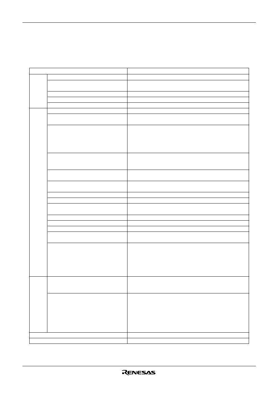
1.3 Performance Outline
Tables 1.1 and 1.2 list performance outline of the M32C/81 group.
Table 1.1 M32C/81 Group Performance (144-Pin Package)
Item
Performance
CPU
Basic instructions
108 instructions
Shortest instruction execution time
31.3 ns (f(BCLK)=32 MHz, V
CC
=4.2 V to 5.5 V)
50ns (f(BCLK)=20MHz, V
CC
=3.0 V to 5.5 V)
Operation mode
Single-chip, memory expansion and microprocessor modes
Memory space
16 Mbytes
Memory capacity
See Table 1.3.
Peripheral Port
123 I/O pins and 1 input pin
function Multifunction timer
Timer A: 16 bits x 5 channels, Timer B: 16 bits x 6 channels
Three-phase motor control circuit
Intelligent I/O
Time measurement function: 16 bits x 12 channels
Waveform generation function: 16 bits x 20 channels
Communication function (Clock synchronous serial I/O, Clock
asynchronous serial I/O, HDLC data processing, Clock synchro-
nous variable length serial I/O, IE bus
(1)
)
Serial I/O
5 channels
Clock synchronous, Clock asynchronous, IEBus
(1)
(option),
I
2
C bus
(2)
(option)
CAN module
1 channel
Supporting CAN 2.0B specification
A-D converter
10-bit A-D converter: 1 circuit
Input : 34 channels
D-A converter
8-bit D-A converter: 2 circuits
DMAC
4 channels
DMAC II
Can be activated by all relocatable vector interrupt factors
Immediate transfer, arithmetic transfer and chain transfer functions
CRC calculation circuit
CRC-CCITT
X-Y converter
16 bits X 16 bits
Watchdog timer
15 bits x 1 channel (with prescaler)
Interrupt
42 internal and 8 external sources, 5 software sources
Interrupt priority level: 7
Clock generation circuit
4 circuits
Main clock generation circuit, sub clock generation circuit, ring
oscillator, PLL frequency synthesizer
The above circuits include an internal feedback resistor and
external ceramic resonator/crystal oscillator.
Main clock oscillator stop detect function
Electric
Supply voltage
4.2 V to 5.5 V (f(BCLK)=32 MHz)
charact-
3.0 V to 5.5 V (f(BCLK)=20 MHz, through VDC)
eristics
3.0 V to 3.6 V (f(BCLK)=20 MHz, not through VDC)
Power consumption
28 mA (V
CC
=5 V, f(BCLK)=32 MHz)
17 mA (V
CC
=3.3 V, f(BCLK)=20 MHz)
470
µ
A (V
CC
=5 V, f(X
CIN
)=32 kHz, in wait mode)
340
µ
A (V
CC
=3.3 V, f(X
CIN
)=32 kHz, through VDC in wait mode)
5.0
µ
A (V
CC
=3.3 V, f(X
CIN
)=32 kHz, not through VDC in wait mode)
0.4
µ
A (V
CC
=5 V, f(X
CIN
)=32 kHz, in stop mode)
0.4
µ
A (V
CC
=3.3 V, f(X
CIN
)=32 kHz, in stop mode)
Operating ambient temperature
≠20 to 85
o
C, ≠40 to 85
o
C (option)
Package
144-pin plastic mold QFP
NOTES:
1. IEBus is a trademark of NEC Electronics Corporation.
2. I
2
C bus is a trademark of Koninklijke Philips Electronics N. V.
All options are on request basis.
M32C/81 Group
1. Overview
Under development
Preliminary specification
Specifications in this manual are tentative and subject to change.
page 4
4
8
f
o
3
0
0
2
,
.
l
u
J
1
0
2
.
0
.
v
e
R
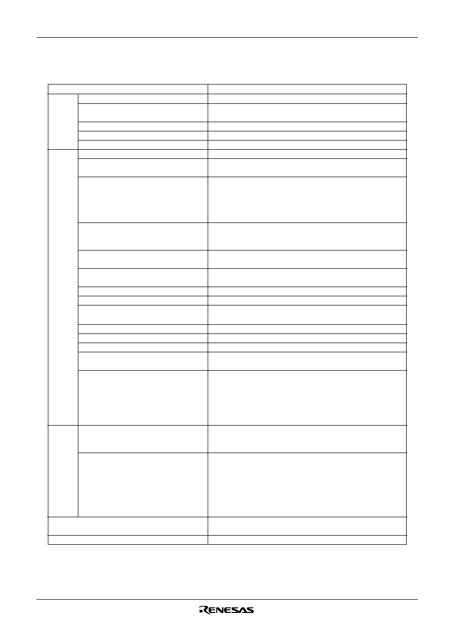
Table 1.2 M32C/81 Group Performance (100-Pin Package)
Item
Performance
CPU
Basic instructions
108 instructions
Shortest instruction execution time
31.3 ns (f(BCLK)=32 MHz, V
CC
=4.2 V to 5.5 V)
50ns (f(BCLK)=20MHz, V
CC
=3.0 V to 5.5 V)
Operation mode
Single-chip, memory expansion and microprocessor modes
Memory space
16 Mbytes
Memory capacity
See Table 1.3.
Peripheral Port
87 I/O pins and 1 input pin
function Multifunction timer
Timer A: 16 bits x 5 channels, Timer B: 16 bits x 6 channels
Three-phase motor control circuit
Intelligent I/O
Time measurement function: 16 bits x 5 channels
Waveform generation function: 16 bits x 8 channels
Communication function (Clock synchronous serial I/O, Clock
asynchronous serial I/O, HDLC data processing, Clock synchro-
nous variable length serial I/O, IE bus
(1)
)
Serial I/O
5 channels
Clock synchronous, Clock asynchronous, IEBus
(1)
(option),
I
2
C bus
(2)
(option)
CAN module
1 channel
Supporting CAN 2.0B specification
A-D converter
10-bit A-D converter: 1 circuit
Input : 26 channels
D-A converter
8-bit D-A converter: 2 circuits
DMAC
4 channels
DMAC II
Can be activated by all relocatable vector interrupt factors
Immediate transfer, arithmetic transfer and chain transfer functions
CRC calculation circuit
CRC-CCITT
X-Y converter
16 bits X 16 bits
Watchdog timer
15 bits x 1 channel (with prescaler)
Interrupt
42 internal and 8 external sources, 5 software sources
Interrupt priority level: 7
Clock generation circuit
4 circuits
Main clock generation circuit, sub clock generation circuit, ring
oscillator, PLL frequency synthesizer
The above circuits include an internal feedback resistor and
external ceramic resonator/crystal oscillator.
Main clock oscillator stop detect function
Electric
Supply voltage
4.2 V to 5.5 V (f(X
IN
)=32 MHz)
charact-
3.0 V to 5.5 V (f(X
IN
)=20 MHz, through VDC)
eristics
3.0 V to 3.6 V (f(X
IN
)=20 MHz, not through VDC)
Power consumption
28 mA (V
CC
=5 V, f(BCLK)=32 MHz)
17 mA (V
CC
=3.3 V, f(BCLK)=20 MHz)
470
µ
A (V
CC
=5 V, f(X
CIN
)=32 kHz, in wait mode)
340
µ
A (V
CC
=3.3 V, f(X
CIN
)=32 kHz, through VDC in wait mode)
5.0
µ
A (V
CC
=3.3 V, f(X
CIN
)=32 kHz, not through VDC in wait mode)
0.4
µ
A (V
CC
=5 V, f(X
CIN
)=32 kHz, in stop mode)
0.4
µ
A (V
CC
=3.3 V, f(X
CIN
)=32 kHz, in stop mode)
Operating ambient temperature
≠20 to 85
o
C
≠40 to 85
o
C (option)
Package
100-pin plastic mold QFP
NOTES:
1. IEBus is a trademark of NEC Electronics Corporation.
2. I
2
C bus is a trademark of Koninklijke Philips Electronics N. V.
All options are on request basis.
M32C/81 Group
1. Overview
Under development
Preliminary specification
Specifications in this manual are tentative and subject to change.
page 5
4
8
f
o
3
0
0
2
,
.
l
u
J
1
0
2
.
0
.
v
e
R
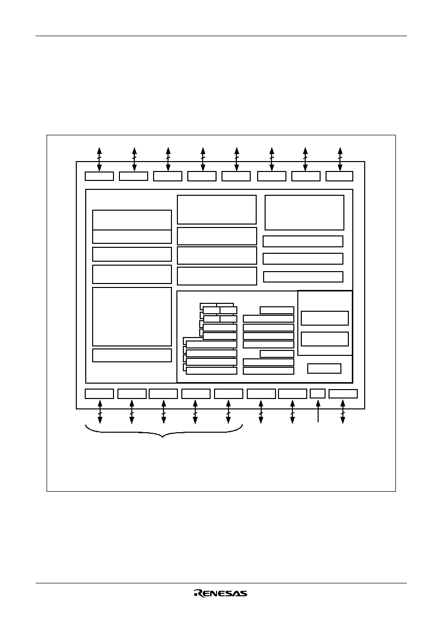
1.4 Block Diagram
Figure 1.1 shows a block diagram of the M32C/81 group.
The M32C/81 group microcomputer contains ROM and RAM as memory to store instructions and data,
CPU to execute calculations and peripheral functions as interrupt, timer, serial I/O, D-A converter, DMAC,
CRC calculation circuit, A-D converter, DRAMC, intelligent I/O and I/O ports.
Figure 1.1 M32C/81 Group Block Diagram
Port P0
Port P1
Port P2
Port P3
Port P4
Port P5
Port P6
Port P7
Port P15
Port P14
Port P13
Port P12
Port P10
Port P9
Port P8
P8
5
Port P11
R0H
R0L
R1H
R1L
R2
R3
A0
A1
FB
SB
NOTES:
1. Ports P11 to P15 are provided in the 144-pin package only.
2. For the 144-pin package only.
FLG
INTB
ISP
USP
PC
SVF
SVP
VCT
Multiplier
M32C/80 series CPU core
Clock generation circuit
X
IN
- X
OUT
X
CIN
- X
COUT
Ring oscillator
PLL frequency synthesizer
A-D converter
1 circuit
Standard 10 inputs
Maximum 34 inputs
UART/Clock synchronous serial I/O
5 channels
X-Y converter
16 bits X 16 bits
CRC arithmetic circuit (CCITT)
X
16
+X
12
+X
5
+1
Timer (16 bits)
Timer A 5 channels
Timer B 6 channels
Three-phase control circuit
Watchdog timer (15 bits)
D-A converter
(8-bit X 2 circuit)
Intelligent I/O
( 3 groups )
Peripheral functions
ROM
RAM
Memory
8
7
8
8
5
(Note1)
8
8
7
8
8
8
8
8
8
8
8
DMAC
DMACII
DRAMC
CAN module
Time measurement 12 channels
2
Wave generation 20 channels
2
Communication function
Clock synchronous serial I/O, UART,
IEBus, HDLC data processing