 | –≠–ª–µ–∫—Ç—Ä–æ–Ω–Ω—ã–π –∫–æ–º–ø–æ–Ω–µ–Ω—Ç: M34502M4 | –°–∫–∞—á–∞—Ç—å:  PDF PDF  ZIP ZIP |
Document Outline
- ˛ˇ
- ˛ˇ
- ˛ˇ
- ˛ˇ
- ˛ˇ
- ˛ˇ
- ˛ˇ
- ˛ˇ
- ˛ˇ
- ˛ˇ
- ˛ˇ
- ˛ˇ
- ˛ˇ
- ˛ˇ
- ˛ˇ
- ˛ˇ
- ˛ˇ
- ˛ˇ
- ˛ˇ
- ˛ˇ
- ˛ˇ
- ˛ˇ
- ˛ˇ
- ˛ˇ
- ˛ˇ
- ˛ˇ
- ˛ˇ
- ˛ˇ
- ˛ˇ
- ˛ˇ
- ˛ˇ
- ˛ˇ
- ˛ˇ
- ˛ˇ
- ˛ˇ
- ˛ˇ
- ˛ˇ
- ˛ˇ
- ˛ˇ
- ˛ˇ
- ˛ˇ
- ˛ˇ
- ˛ˇ
- ˛ˇ
- ˛ˇ
- ˛ˇ
- ˛ˇ
- ˛ˇ
- ˛ˇ
- ˛ˇ
- ˛ˇ
- ˛ˇ
- ˛ˇ
- ˛ˇ
- ˛ˇ
- ˛ˇ
- ˛ˇ

Regarding the change of names mentioned in the document, such as Mitsubishi
Electric and Mitsubishi XX, to Renesas Technology Corp.
The semiconductor operations of Hitachi and Mitsubishi Electric were transferred to Renesas
Technology Corporation on April 1st 2003. These operations include microcomputer, logic, analog
and discrete devices, and memory chips other than DRAMs (flash memory, SRAMs etc.)
Accordingly, although Mitsubishi Electric, Mitsubishi Electric Corporation, Mitsubishi
Semiconductors, and other Mitsubishi brand names are mentioned in the document, these names
have in fact all been changed to Renesas Technology Corp. Thank you for your understanding.
Except for our corporate trademark, logo and corporate statement, no changes whatsoever have been
made to the contents of the document, and these changes do not constitute any alteration to the
contents of the document itself.
Note : Mitsubishi Electric will continue the business operations of high frequency & optical devices
and power devices.
Renesas Technology Corp.
Customer Support Dept.
April 1, 2003
To all our customers
DESCRIPTION
The 4502 Group is a 4-bit single-chip microcomputer designed with
CMOS technology. Its CPU is that of the 4500 series using a
simple, high-speed instruction set. The computer is equipped with
two 8-bit timers (each timer has a reload register), interrupts, and
10-bit A-D converter.
The various microcomputers in the 4502 Group include variations
of the built-in memory size as shown in the table below.
FEATURES
q
Minimum instruction execution time ................................ 0.68
µ
s
(at 4.4 MHz oscillation frequency, in high-speed mode)
q
Supply voltage ......................................................... VRST to 5.5 V
(VRST: detection voltage of voltage drop detection circuit)
Product
M34502M2-XXXFP
M34502M4-XXXFP
M34502E4FP (Note)
ROM type
Mask ROM
Mask ROM
One Time PROM
Package
24P2Q-A
24P2Q-A
24P2Q-A
RAM size
(
4 bits)
128 words
256 words
256 words
ROM (PROM) size
(
10 bits)
2048 words
4096 words
4096 words
4502 Group
SINGLE-CHIP 4-BIT CMOS MICROCOMPUTER
MITSUBISHI MICROCOMPUTERS
q
Timers
Timer 1 ...................................... 8-bit timer with a reload register
Timer 2 ...................................... 8-bit timer with a reload register
q
Interrupt ........................................................................ 4 sources
q
Key-on wakeup function pins ................................................... 12
q
Input/Output port ...................................................................... 18
q
A-D converter .................. 10-bit successive comparison method
q
Watchdog timer
q
Clock generating circuit (ceramic resonator/RC oscillation)
q
LED drive directly enabled (port D)
q
Power-on reset circuit
q
Voltage drop detection circuit ........................... VRST: Typ. 3.5 V
(Ta = 25 ∞C)
APPLICATION
Electrical household appliance, consumer electronic products, of-
fice automation equipment, etc.
Note: Shipped in blank.
2
4502 Group
SINGLE-CHIP 4-BIT CMOS MICROCOMPUTER
MITSUBISHI MICROCOMPUTERS
PIN CONFIGURATION
17
1
8
2
1
2
0
2
2
19
2
3
2
4
1
6
1
5
14
1
3
V
D
D
P
1
0
P1
1
P
1
2
/
C
N
T
R
P1
3
/INT
P0
3
P
0
2
P
0
1
P
0
0
V
S
S
D
4
D
5
X
I
N
X
OUT
C
N
V
S
S
P
2
1
/
A
I
N
1
P2
0
/A
IN0
M
3
4
5
0
2
RESET
D
2
/C
D
3
/
K
D
1
D
0
P
3
1
/
A
I
N
3
P
3
0
/
A
I
N
2
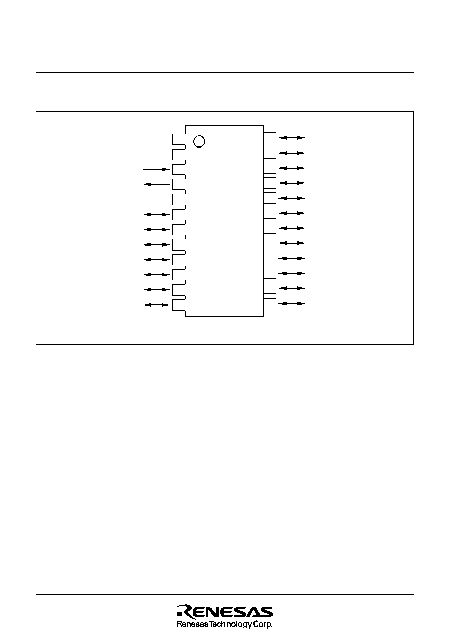
Outline 24P2Q-A
M
3
4
5
0
2
M
x
-
X
X
X
F
P
M
3
4
5
0
2
E
4
F
P
8
7
4
5
3
6
2
1
9
1
0
1
1
12
Pin configuration (top view) (4502 Group)
3
4502 Group
SINGLE-CHIP 4-BIT CMOS MICROCOMPUTER
MITSUBISHI MICROCOMPUTERS
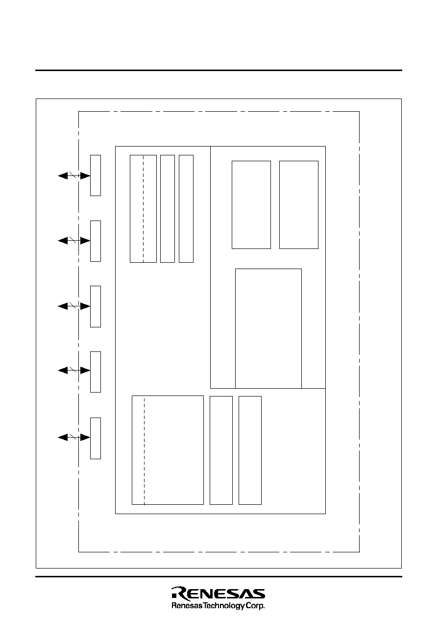
Block diagram (4502 Group)
R
A
M
R
O
M
M
e
m
o
r
y
I
/
O
p
o
r
t
I
n
t
e
r
n
a
l
p
e
r
i
p
h
e
r
a
l
f
u
n
c
t
i
o
n
s
T
i
m
e
r
T
i
m
e
r
1
(
8
b
i
t
s
)
S
y
s
t
e
m
c
l
o
c
k
g
e
n
e
r
a
t
i
n
g
c
i
r
c
u
i
t
T
i
m
e
r
2
(
8
b
i
t
s
)
1
2
8
,
2
5
6
w
o
r
d
s
4
b
i
t
s
2
0
4
8
,
4
0
9
6
w
o
r
d
s
1
0
b
i
t
s
4
5
0
0
S
e
r
i
e
s
C
P
U
c
o
r
e
R
e
g
i
s
t
e
r
B
(
4
b
i
t
s
)
R
e
g
i
s
t
e
r
A
(
4
b
i
t
s
)
R
e
g
i
s
t
e
r
D
(
3
b
i
t
s
)
R
e
g
i
s
t
e
r
E
(
8
b
i
t
s
)
S
t
a
c
k
r
e
g
i
s
t
e
r
S
K
(
8
l
e
v
e
l
s
)
I
n
t
e
r
r
u
p
t
s
t
a
c
k
r
e
g
i
s
t
e
r
S
D
P
(
1
l
e
v
e
l
)
A
L
U
(
4
b
i
t
s
)
X
I
N
-
X
O
U
T
W
a
t
c
h
d
o
g
t
i
m
e
r
(
1
6
b
i
t
s
)
(
1
0
b
i
t
s
4
c
h
)
A
-
D
c
o
n
v
e
r
t
e
r
P
o
r
t
P
0
4
P
o
r
t
P
1
4
P
o
r
t
P
2
2
P
o
r
t
D
6
P
o
w
e
r
-
o
n
r
e
s
e
t
c
i
r
c
u
i
t
V
o
l
t
a
g
e
d
r
o
p
d
e
t
e
c
t
i
o
n
c
i
r
c
u
i
t
P
o
r
t
P
3
2
4
4502 Group
SINGLE-CHIP 4-BIT CMOS MICROCOMPUTER
MITSUBISHI MICROCOMPUTERS
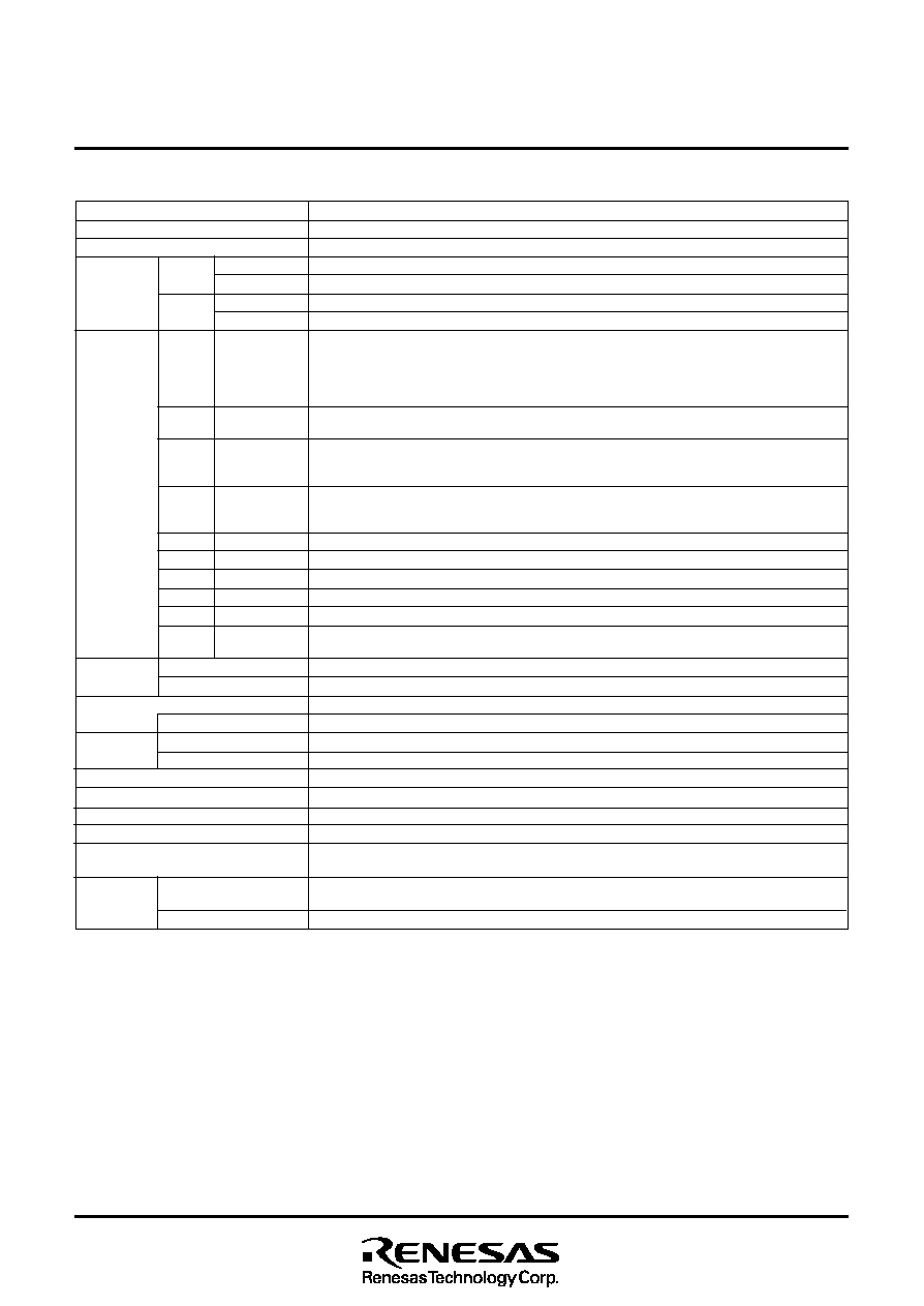
PERFORMANCE OVERVIEW
Function
113
0.68
µ
s (at 4.4 MHz oscillation frequency, in high-speed mode)
2048 words
10 bits
4096 words
10 bits
128 words
4 bits
256 words
4 bits
Six independent I/O ports.
Input is examined by skip decision.
Ports D
2
and D
3
are equipped with a pull-up function and a key-on wakeup function. Both func-
tions can be switched by software.
Ports D
2
and D
3
are also used as ports C and K, respectively.
4-bit I/O port; each pin is equipped with a pull-up function and a key-on wakeup function. Both
functions can be switched by software.
4-bit I/O port; each pin is equipped with a pull-up function and a key-on wakeup function. Both
functions can be switched by software.
Ports P1
2
and P1
3
are also used as CNTR and INT, respectively.
2-bit I/O port; each pin is equipped with a pull-up function and a key-on wakeup function. Both
functions can be switched by software.
Ports P2
0
and P2
1
are also used as A
IN0
and A
IN1
, respectively.
2-bit I/O port; Ports P3
0
and P3
1
are also used as A
IN2
and A
IN3
, respectively.
1-bit I/O; Port C is also used as port D
2
.
1-bit I/O; Port K is also used as port D
3
.
1-bit I/O; CNTR pin is also used as port P1
2
.
1-bit input; INT pin is also used as port P1
3
.
Four independent I/O ports. A
IN0
≠A
IN3
is also used as ports P2
0
, P2
1
, P3
0
, P3
1
, respectively.
8-bit programmable timer with a reload register.
8-bit programmable timer with a reload register and has a event counter.
10-bit wide, This is equipped with an 8-bit comparator function.
4 channel (A
IN0
pin≠A
IN3
pin)
4 (one for external, two for timer, one for A-D)
1 level
8 levels
CMOS silicon gate
24-pin plastic molded SSOP (24P2Q-A)
≠20 ∞C to 85 ∞C
VRST to 5.5 V (VRST: detected voltage of voltage drop detection circuit. Refer to the voltage
drop detection circuit characteristics.)
1.7 mA (at V
DD
= 5.0 V, 4.0 MHz oscillation frequency, in high-speed mode, output transistors
in the cut-off state)
0.1
µ
A (at room temperature, V
DD
= 5 V, output transistors in the cut-off state)
Parameter
Number of basic instructions
Minimum instruction execution time
Memory sizes
Input/Output
ports
ROM
RAM
D
0
≠D
5
P0
0
≠P0
3
P1
0
≠P1
3
P2
0
, P2
1
P3
0
, P3
1
C
K
CNTR
INT
A
IN0
, A
IN1
A
IN2
, A
IN3
Timer 1
Timer 2
Analog input
Sources
Nesting
Active mode
RAM back-up mode
M34502M2
M34502M4/E4
M34502M2
M34502M4/E4
I/O
I/O
I/O
I/O
I/O
I/O
I/O
Timer I/O
Interrupt input
Analog input
Timers
A-D converter
Interrupt
Subroutine nesting
Device structure
Package
Operating temperature range
Supply voltage
Power
dissipation
(typical value)