Document Outline
- ˛ˇ
- ˛ˇ
- ˛ˇ
- ˛ˇ
- ˛ˇ
- ˛ˇ
- ˛ˇ
- ˛ˇ
- ˛ˇ
- ˛ˇ
- ˛ˇ
- ˛ˇ
- ˛ˇ
- ˛ˇ
- ˛ˇ
- ˛ˇ
- ˛ˇ
- ˛ˇ
- ˛ˇ
- ˛ˇ
- ˛ˇ
- ˛ˇ
- ˛ˇ
- ˛ˇ
- ˛ˇ
- ˛ˇ
- ˛ˇ
- ˛ˇ
- ˛ˇ
- ˛ˇ
- ˛ˇ
- ˛ˇ
- ˛ˇ
- ˛ˇ
- ˛ˇ
- ˛ˇ
- ˛ˇ
- ˛ˇ
- ˛ˇ
- ˛ˇ
- ˛ˇ
- ˛ˇ
- ˛ˇ
- ˛ˇ
- ˛ˇ
- ˛ˇ
- ˛ˇ
- ˛ˇ
- ˛ˇ
- ˛ˇ
- ˛ˇ
- ˛ˇ
- ˛ˇ
- ˛ˇ
- ˛ˇ
- ˛ˇ
- ˛ˇ
- ˛ˇ
- ˛ˇ
- ˛ˇ
- ˛ˇ
- ˛ˇ
- ˛ˇ
- ˛ˇ
DESCRIPTION
The 4519 Group is a 4-bit single-chip microcomputer designed with
CMOS technology. Its CPU is that of the 4500 series using a
simple, high-speed instruction set. The computer is equipped with
serial I/O, four 8-bit timers (each timer has one or two reload regis-
ter), a 10-bit A-D converter, interrupts, and oscillation circuit switch
function.
The various microcomputers in the 4519 Group include variations
of the built-in memory size as shown in the table below.
FEATURES
Minimum instruction execution time .................................. 0.5
µ
s
(at 6 MHz oscillation frequency, in X
IN
through-mode)
Supply voltage
Mask ROM version ...................................................... 1.8 to 5.5 V
One Time PROM version ............................................. 2.5 to 5.5 V
(It depends on operation source clock, oscillation frequency and op-
eration mode)
Timers
Timer 1 ...................................... 8-bit timer with a reload register
Timer 2 ...................................... 8-bit timer with a reload register
Timer 3 ...................................... 8-bit timer with a reload register
Timer 3 ................................. 8-bit timer with two reload registers
Product
M34519M6-XXXFP
M34519M8-XXXFP
M34519E8FP (Note)
ROM type
Mask ROM
Mask ROM
One Time PROM
Package
42P2R-A
42P2R-A
42P2R-A
RAM size
(
4 bits)
384 words
384 words
384 words
ROM (PROM) size
(
10 bits)
6144 words
8192 words
8192 words
Interrupt ........................................................................ 8 sources
Key-on wakeup function pins ................................................... 10
Serial I/O ....................................................................... 8 bits
1
A-D converter ...... 10-bit successive approximation method, 8ch
Voltage drop detection circuit
Reset occurrence .................................... Typ. 3.5 V (Ta = 25 ∞C)
Reset release .......................................... Typ. 3.7 V (Ta = 25 ∞C)
Watchdog timer
Clock generating circuit
(ceramic resonator/RC oscillation/quartz-crystal oscillation/inter-
nal ring oscillator)
LED drive directly enabled (port D)
APPLICATION
Electrical household appliance, consumer electronic products, of-
fice automation equipment, etc.
Note: Shipped in blank.
Rev.2.00 2003.04.15 page 1 of 159
4519 Group
SINGLE-CHIP 4-BIT CMOS MICROCOMPUTER
REJ03B0007-0200Z
Rev.2.00
2003.04.15

PRELIMINARY
Notice: This is not a final specification.
Some parametric limits are subject to change.
Rev.2.00 2003.04.15 page 2 of 159
4519 Group
PIN CONFIGURATION
Pin configuration (top view) (4519 Group)
OUTLINE 42P2R-A
M34519Mx-XXXFP
M34519E8FP
8
7
10
9
12
11
14
15
16
13
17
19
20
21
18
6
5
4
3
2
1
35
36
33
34
31
32
29
28
27
30
26
24
23
22
25
37
38
39
40
41
42
P1
2
P1
1
P1
0
P0
3
P0
2
P0
1
P0
0
P4
3
/A
IN7
P4
2
/A
IN6
P4
1
/A
IN5
P4
0
/A
IN4
P6
3
/A
IN3
P6
2
/A
IN2
P6
1
/A
IN1
P6
0
/A
IN0
P3
3
P3
2
P3
1
/INT1
P3
0
/INT0
VDCE
V
DD
P1
3
D
0
D
1
D
2
D
3
D
4
D
5
D
6
/CNTR
0
D
7
/CNTR
1
P5
0
P5
1
P5
2
P5
3
P2
0
/S
CK
P2
1
/S
OUT
P2
2
/S
IN
RESET
CNV
SS
X
OUT
X
IN
V
SS
PRELIMINARY
Notice: This is not a final specification.
Some parametric limits are subject to change.
Rev.2.00 2003.04.15 page 3 of 159
4519 Group
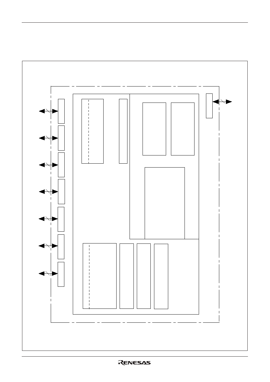
Block diagram (4519 Group)
4
4
3
4
4
8
R
A
M
R
O
M
M
e
m
o
r
y
I
/
O
p
o
r
t
I
n
t
e
r
n
a
l
p
e
r
i
p
h
e
r
a
l
f
u
n
c
t
i
o
n
s
T
i
m
e
r
T
i
m
e
r
1
(
8
b
i
t
s
)
S
y
s
t
e
m
c
l
o
c
k
g
e
n
e
r
a
t
i
o
n
c
i
r
c
u
i
t
T
i
m
e
r
2
(
8
b
i
t
s
)
3
8
4
w
o
r
d
s
4
b
i
t
s
6
1
4
4
,
8
1
9
2
w
o
r
d
s
1
0
b
i
t
s
4
5
0
0
s
e
r
i
e
s
C
P
U
c
o
r
e
R
e
g
i
s
t
e
r
B
(
4
b
i
t
s
)
R
e
g
i
s
t
e
r
A
(
4
b
i
t
s
)
R
e
g
i
s
t
e
r
D
(
3
b
i
t
s
)
R
e
g
i
s
t
e
r
E
(
8
b
i
t
s
)
S
t
a
c
k
r
e
g
i
s
t
e
r
S
K
(
8
l
e
v
e
l
s
)
I
n
t
e
r
r
u
p
t
s
t
a
c
k
r
e
g
i
s
t
e
r
S
D
P
(
1
l
e
v
e
l
)
A
L
U
(
4
b
i
t
s
)
W
a
t
c
h
d
o
g
t
i
m
e
r
(
1
6
b
i
t
s
)
P
o
r
t
P
0
P
o
r
t
P
1
P
o
r
t
P
2
V
o
l
t
a
g
e
d
r
o
p
d
e
t
e
c
t
i
o
n
c
i
r
c
u
i
t
T
i
m
e
r
3
(
8
b
i
t
s
)
T
i
m
e
r
4
(
8
b
i
t
s
)
X
I
N
-
X
O
U
T
(
C
e
r
a
m
i
c
/
Q
u
a
r
t
z
-
c
r
y
s
t
a
l
/
R
C
)
B
u
i
l
t
-
i
n
r
i
n
g
o
s
c
i
l
l
a
t
o
r
P
o
r
t
P
3
P
o
r
t
D
P
o
r
t
P
6
S
e
r
i
a
l
I
/
O
(
8
b
i
t
s
1
)
A
-
D
c
o
n
v
e
r
t
e
r
(
1
0
b
i
t
s
8
c
h
)
4
P
o
r
t
P
4
4
P
o
r
t
P
5
PRELIMINARY
Notice: This is not a final specification.
Some parametric limits are subject to change.
Rev.2.00 2003.04.15 page 4 of 159
4519 Group
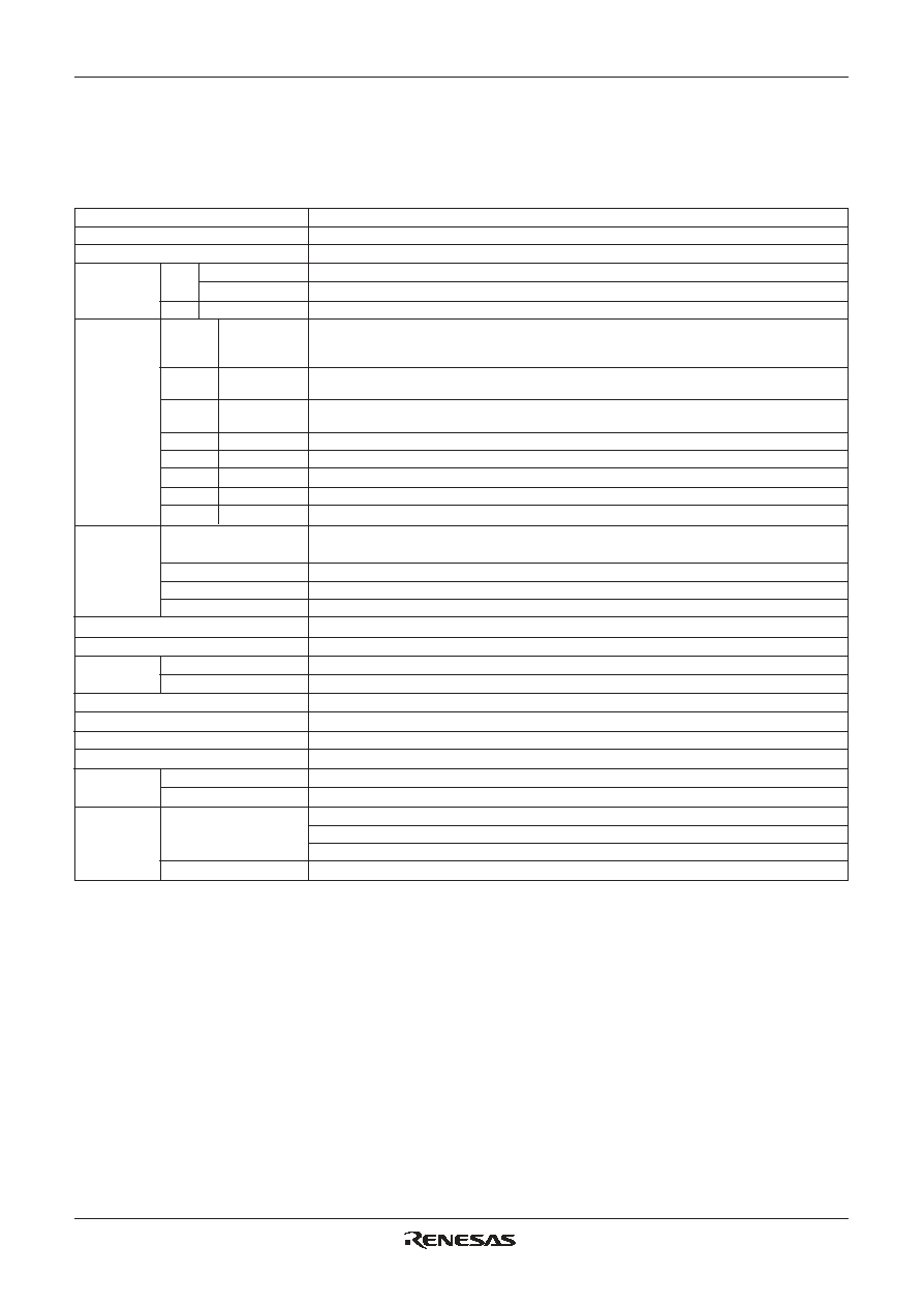
PERFORMANCE OVERVIEW
Function
153
0.5
µ
s (at 6.0 MHz oscillation frequency, in X
IN
through-mode)
6144 words
10 bits
8192 words
10 bits
384 words
4 bits
Eight independent I/O ports;
Ports D
6
and D
7
are also used as CNTR0 and CNTR1, respectively.
The output structure is switched by software.
4-bit I/O port; a pull-up function, a key-on wakeup function and output structure can be switched
by software.
4-bit I/O port; a pull-up function, a key-on wakeup function and output structure can be switched
by software.
3-bit I/O port; ports P2
0
, P2
1
and P2
2
are also used as S
CK
, S
OUT
and S
IN
, respectively.
4-bit I/O port ; ports P3
0
and P3
1
are also used as INT0 and INT1, respectively.
4-bit I/O port ; ports P4
0
≠P4
3
are also used as A
IN4
≠A
IN7
, respectively.
4-bit I/O port ; the output structure is switched by software.
4-bit I/O port ; ports P6
0
≠P6
3
are also used as A
IN0
≠A
IN3
, respectively.
8-bit timer with a reload register is also used as an event counter.
Also, this is equipped with a period/pulse width measurement function.
8-bit timer with a reload register.
8-bit timer with a reload register is also used as an event counter.
8-bit timer with two reload registers and PWM output function.
10-bit wide
8 ch, This is equipped with an 8-bit comparator function.
8-bit
1
8 (two for external, four for timer, one for A-D, and one for serial I/O)
1 level
8 levels
CMOS silicon gate
42-pin plastic molded SSOP (42P2R-A)
≠20 ∞C to 85 ∞C
1.8 V to 5.5 V (It depends on operation source clock, oscillation frequency and operating mode.)
2.5 V to 5.5 V (It depends on operation source clock, oscillation frequency and operating mode.)
2.8 mA (V
DD
=5V, f(X
IN
)=6 MHz, f(STCK)=f(X
IN
), ring oscillator stop)
70
µ
A (V
DD
=5V, f(X
IN
)=32 kHz, f(STCK)=f(X
IN
), ring oscillator stop)
150
µ
A (V
DD
=5V, ring oscillator is used, f(STCK)=f(RING), f(X
IN
) stop)
0.1
µ
A (at room temperature, V
DD
= 5 V, output transistors in the cut-off state)
Parameter
Number of basic instructions
Minimum instruction execution time
Memory sizes
Input/Output
ports
Timers
A-D converter
Serial I/O
Interrupt
Subroutine nesting
Device structure
Package
Operating temperature range
Supply voltage
Power
dissipation
(typical value)
ROM
RAM
D
0
≠D
7
P0
0
≠P0
3
P1
0
≠P1
3
P2
0
≠P2
2
P3
0
≠P3
3
P4
0
≠P4
3
P5
0
≠P5
3
P6
0
≠P6
3
Timer 1
Timer 2
Timer 3
Timer 4
Sources
Nesting
Mask ROM version
One Time PROM version
Active mode
RAM back-up mode
I/O (Input is
examined by
skip decision)
I/O
I/O
I/O
I/O
I/O
I/O
I/O
M34519M6
M34519M8/E8
M34519M6/M8/E8
PRELIMINARY
Notice: This is not a final specification.
Some parametric limits are subject to change.
Rev.2.00 2003.04.15 page 5 of 159
4519 Group
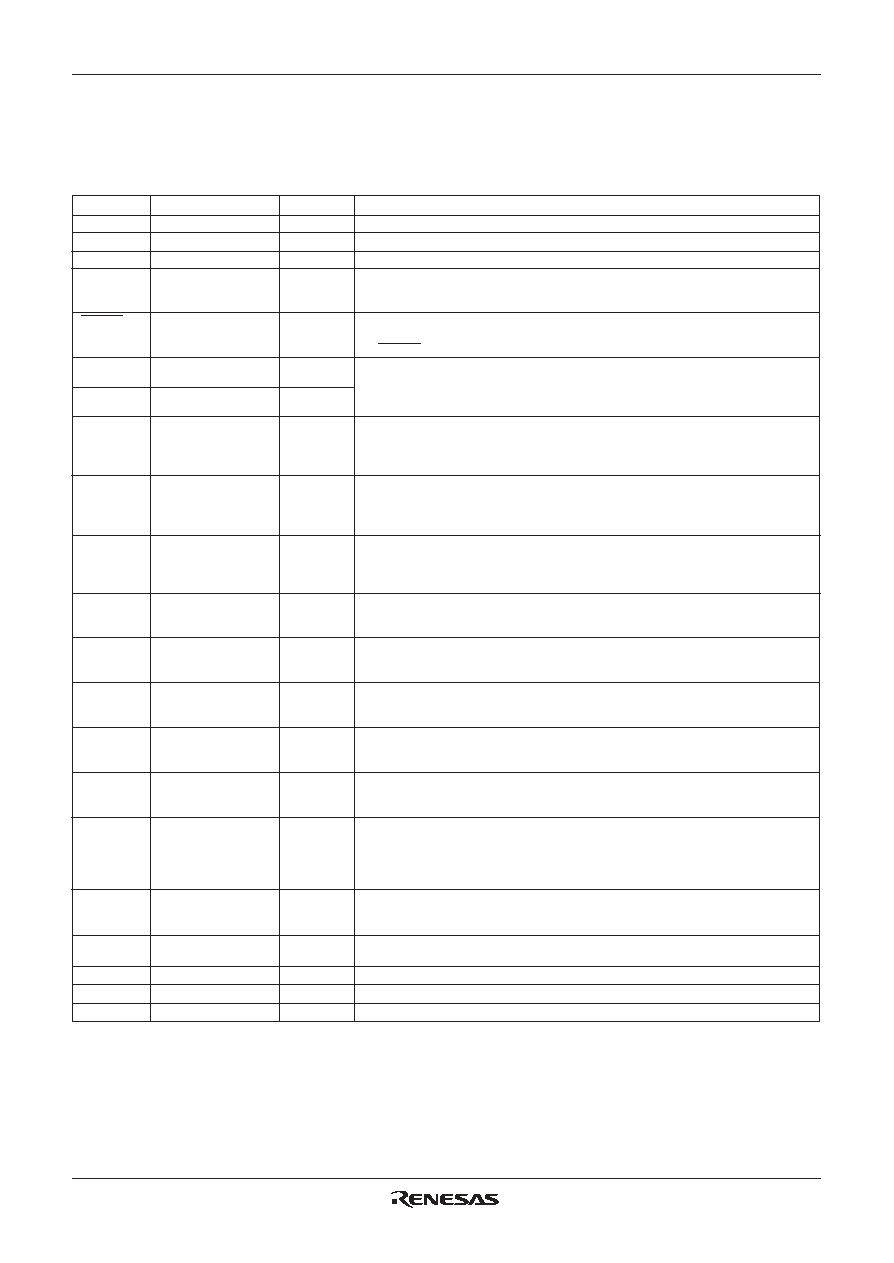
PIN DESCRIPTION
Name
Power supply
Ground
CNV
SS
Voltage drop
detection circuit
enable
Reset input/output
Main clock input
Pin
V
DD
V
SS
CNV
SS
VDCE
RESET
X
IN
Input/Output
--
--
--
Input
I/O
Input
Function
Connected to a plus power supply.
Connected to a 0 V power supply.
Connect CNV
SS
to V
SS
and apply "L" (0V) to CNV
SS
certainly.
This pin is used to operate/stop the voltage drop detection circuit. When "H" level is
input to this pin, the circuit starts operating. When "L" level is input to this pin, the
circuit stops operating.
An N-channel open-drain I/O pin for a system reset. When the SRST instruction,
watchdog timer or the voltage drop detection circuit cause the system to be reset,
the
RESET
pin outputs "L" level.
I/O pins of the main clock generating circuit. When using a ceramic resonator, connect
it between pins X
IN
and X
OUT
. When using a 32 kHz quartz-crystal oscillator, connect it
between pins X
IN
and X
OUT
. A feedback resistor is built-in between them. When using
the RC oscillation, connect a resistor and a capacitor to X
IN
, and leave X
OUT
pin open.
X
OUT
Main clock output
Output
D
0
≠D
7
P0
0
≠P0
3
P1
0
≠P1
3
P2
0
≠P2
3
P3
0
≠P3
3
P4
0
≠P4
3
P5
0
≠P5
3
P6
0
≠P6
3
CNTR0,
CNTR1
INT0, INT1
A
IN0
≠A
IN7
S
CK
S
OUT
S
IN
I/O port D
Input is examined by
skip decision.
I/O port P0
I/O port P1
I/O port P2
I/O port P3
I/O port P4
I/O port P5
I/O port P6
Timer input/output
Interrupt input
Analog input
Serial I/O data I/O
Serial I/O data output
Serial I/O clock input
I/O
I/O
I/O
I/O
I/O
I/O
I/O
I/O
I/O
Input
Input
I/O
Output
Input
Each pin of port D has an independent 1-bit wide I/O function. The output structure
can be switched to N-channel open-drain or CMOS by software. For input use, set
the latch of the specified bit to "1" and select the N-channel open-drain. Ports D
6
, D
7
is also used as CNTR0 pin and CNTR1 pin, respectively.
P
ort P0 serves as a 4-bit I/O port. The output structure can be switched to N-channel
open-drain or CMOS by software. For input use, set the latch of the specified bit to
"1" and select the N-channel open-drain. Port P0 has a key-on wakeup function and
a pull-up function. Both functions can be switched by software.
P
ort P1 serves as a 4-bit I/O port. The output structure can be switched to N-channel
open-drain or CMOS by software. For input use, set the latch of the specified bit to
"1" and select the N-channel open-drain. Port P1 has a key-on wakeup function and
a pull-up function. Both functions can be switched by software.
P
ort P2 serves as a 3-bit I/O port. The output structure is N-channel open-drain. For
input use, set the latch of the specified bit to "1".
Ports P2
0
≠P2
2
are also used as S
CK
, S
OUT
, S
IN
, respectively.
P
ort P3 serves as a 4-bit I/O port. The output structure is N-channel open-drain. For
input use, set the latch of the specified bit to "1".
Ports P3
0
and P3
1
are also used as INT0 pin and INT1 pin, respectively.
P
ort P4 serves as a 4-bit I/O port. The output structure can be switched to N-channel
open-drain. For input use, set the latch of the specified bit to "1". Ports P4
0
≠P4
3
are
also used as A
IN4
≠A
IN7
, respectively.
P
ort P5 serves as a 4-bit I/O port. The output structure can be switched to N-channel
open-drain or CMOS by software. For input use, set the latch of the specified bit to
"1" and select the N-channel open-drain.
P
ort P6 serves as a 4-bit I/O port. The output structure can be switched to N-channel
open-drain. For input use, set the latch of the specified bit to "1". Ports P6
0
≠P6
3
are
also used as A
IN0
≠A
IN3
, respectively.
CNTR0 pin has the function to input the clock for the timer 1 event counter, and to
output the timer 1 or timer 2 underflow signal divided by 2.
CNTR1 pin has the function to input the clock for the timer 3 event counter, and to
output the PWM signal generated by timer 4.CNTR0 pin and CNTR1 pin are also
used as Ports D
6
and D
7
, respectively.
INT0 pin and INT1 pin accept external interrupts. They have the key-on wakeup func-
tion which can be switched by software. INT0 pin and INT1 pin are also used as
Ports P3
0
and P3
1
, respectively.
A-D converter analog input pins. A
IN0
≠A
IN7
are also used as ports P6
0
≠P6
3
and P4
0
≠
P4
3
, respectively.
Serial I/O data transfer synchronous clock I/O pin. S
CK
pin is also used as port P2
0.
.
Serial I/O data output pin. S
OUT
pin is also used as port P2
1
.
Serial I/O data input pin. S
IN
pin is also used as port P2
2
.