Document Outline
- ˛ˇ
- ˛ˇ
- ˛ˇ
- ˛ˇ
- ˛ˇ
- ˛ˇ
- ˛ˇ
- ˛ˇ
- ˛ˇ
- ˛ˇ
- ˛ˇ
- ˛ˇ
- ˛ˇ
- ˛ˇ
- ˛ˇ
- ˛ˇ
- ˛ˇ
- ˛ˇ
- ˛ˇ
- ˛ˇ
- ˛ˇ
- ˛ˇ
- ˛ˇ
- ˛ˇ
- ˛ˇ
- ˛ˇ
- ˛ˇ
- ˛ˇ
- ˛ˇ
- ˛ˇ
- ˛ˇ
- ˛ˇ
- ˛ˇ
- ˛ˇ
- ˛ˇ
- ˛ˇ
- ˛ˇ
- ˛ˇ
- ˛ˇ

Regarding the change of names mentioned in the document, such as Mitsubishi
Electric and Mitsubishi XX, to Renesas Technology Corp.
The semiconductor operations of Hitachi and Mitsubishi Electric were transferred to Renesas
Technology Corporation on April 1st 2003. These operations include microcomputer, logic, analog
and discrete devices, and memory chips other than DRAMs (flash memory, SRAMs etc.)
Accordingly, although Mitsubishi Electric, Mitsubishi Electric Corporation, Mitsubishi
Semiconductors, and other Mitsubishi brand names are mentioned in the document, these names
have in fact all been changed to Renesas Technology Corp. Thank you for your understanding.
Except for our corporate trademark, logo and corporate statement, no changes whatsoever have been
made to the contents of the document, and these changes do not constitute any alteration to the
contents of the document itself.
Note : Mitsubishi Electric will continue the business operations of high frequency & optical devices
and power devices.
Renesas Technology Corp.
Customer Support Dept.
April 1, 2003
To all our customers

DESCRIPTION
The 4524 Group is a 4-bit single-chip microcomputer designed with
CMOS technology. Its CPU is that of the 4500 series using a
simple, high-speed instruction set. The computer is equipped with
main clock selection function, serial I/O, four 8-bit timers (each
timer has one or two reload register), 10-bit A-D converter, inter-
rupts, and LCD control circuit.
The various microcomputers in the 4524 Group include variations
of the built-in memory size as shown in the table below.
FEATURES
q
Minimum instruction execution time .................................. 0.5
µ
s
(at 6 MHz oscillation frequency, in high-speed through-mode)
q
Supply voltage
Mask ROM version ...................................................... 2.0 to 5.5 V
One Time PROM version ............................................. 2.5 to 5.5 V
(It depends on oscillation frequency and operation mode)
q
Timers
Timer 1 ...................................... 8-bit timer with a reload register
Timer 2 ...................................... 8-bit timer with a reload register
Timer 3 ...................................... 8-bit timer with a reload register
Timer 4 ................................. 8-bit timer with two reload registers
Timer 5 .............................. 16-bit timer (fixed dividing frequency)
Product
M34524M8-XXXFP
M34524MC-XXXFP
M34524EDFP (Note)
ROM type
Mask ROM
Mask ROM
One Time PROM
Package
64P6N-A
64P6N-A
64P6N-A
RAM size
(
4 bits)
512 words
512 words
512 words
ROM (PROM) size
(
10 bits)
8192 words
12288 words
16384 words
4524 Group
SINGLE-CHIP 4-BIT CMOS MICROCOMPUTER
MITSUBISHI MICROCOMPUTERS
q
Interrupt ........................................................................ 9 sources
q
Key-on wakeup function pins ................................................... 10
q
LCD control circuit
Segment output ........................................................................ 20
Common output .......................................................................... 4
q
Serial I/O ......................................................................... 8-bit
1
q
A-D converter .............. 10-bit successive approximation method
q
Voltage drop detection circuit (Reset) ......................... Typ. 3.5 V
q
Watchdog timer
q
Clock generating circuit
Main clock
(ceramic resonator/RC oscillation/internal ring oscillator)
Sub-clock
(quartz-crystal oscillation)
q
LED drive directly enabled (port D)
APPLICATION
Household appliance, consumer electronics, office automation
equipment
Note: Shipped in blank.
PRELIMINAR
Y
Notice: This is not a final specification.
Som
e parametric limits are subject to change.
2
4524 Group
SINGLE-CHIP 4-BIT CMOS MICROCOMPUTER
MITSUBISHI MICROCOMPUTERS
PRELIMINAR
Y
Notice: This is not a final specification.
Some parametric limits are subject to change.
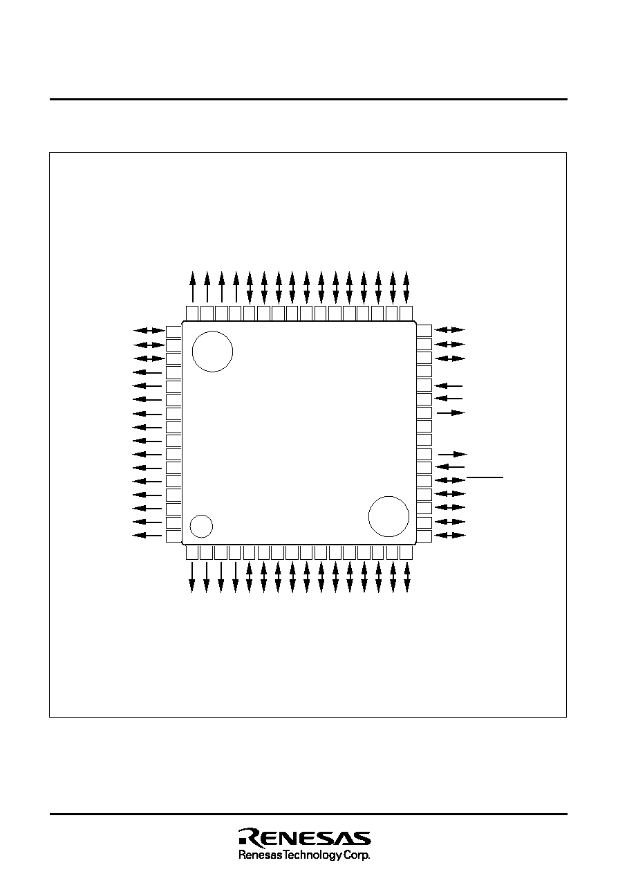
PIN CONFIGURATION
Pin configuration (top view) (4524 Group)
OUTLINE 64P6N-A
6
4
4
9
50
5
1
5
2
53
5
4
55
56
5
7
58
5
9
6
0
61
6
2
63
7
8
9
10 11 1
2 13 1
4 15 1
6
3
4
5
6
1
2
17
3
2
31
30
2
9
2
8
27
2
6
2
5
24
23
2
2
21
20
1
9
1
8
D
3
P
3
1
/
A
I
N
5
P
3
0
/
A
I
N
4
P
0
0
P
0
1
P
0
2
P
0
3
P
1
1
P
1
3
P
1
0
P
1
2
D
1
D
2
R
E
S
E
T
P
3
3
/
A
I
N
7
P
3
2
/
A
I
N
6
X
C
O
U
T
X
CIN
C
N
V
S
S
X
O
U
T
X
IN
V
SS
V
D
D
D
5
/
S
O
U
T
D
4
/
S
I
N
4
8 4
7
4
2 4
1 4
0 39 3
8 3
7 3
6 35 3
4 3
3
46 45 44 43
SEG
14
S
E
G
1
5
S
E
G
1
3
SEG
12
D
0
V
D
C
E
P
2
1
/
A
I
N
1
P
2
2
/
A
I
N
2
S
E
G
6
S
E
G
5
SEG
4
S
E
G
3
V
LC
1
/SEG
2
V
L
C
2
/
S
E
G
1
V
L
C
3
/
S
E
G
0
C
O
M
0
C
O
M
1
C
O
M
2
C
O
M
3
S
E
G
7
SEG
8
S
E
G
9
S
E
G
1
1
P
2
3
/
A
I
N
3
SEG
10
S
E
G
1
6
D
7
/CNTR0
C
/
C
N
T
R
1
D
8
/INT0
D
9
/
I
N
T
1
D
6
/S
CK
M34524Mx-XXXFP
M34524EDFP
S
E
G
1
9
P
2
0
/
A
I
N
0
S
E
G
1
7
S
E
G
1
8
P
4
1
P
4
0
P
4
3
P
4
2

3
4524 Group
SINGLE-CHIP 4-BIT CMOS MICROCOMPUTER
MITSUBISHI MICROCOMPUTERS
PRELIMINAR
Y
Notice: This is not a final specification.
Some parametric limits are subject to change.
Block diagram (4524 Group)
4
4
4
2
0
4
4
4
8
1
2
R
A
M
R
O
M
M
e
m
o
r
y
I
/
O
p
o
r
t
I
n
t
e
r
n
a
l
p
e
r
i
p
h
e
r
a
l
f
u
n
c
t
i
o
n
s
T
i
m
e
r
T
i
m
e
r
1
(
8
b
i
t
s
)
S
y
s
t
e
m
c
l
o
c
k
g
e
n
e
r
a
t
i
o
n
c
i
r
c
u
i
t
T
i
m
e
r
2
(
8
b
i
t
s
)
5
1
2
w
o
r
d
s
4
b
i
t
s
L
C
D
d
i
s
p
l
a
y
R
A
M
i
n
c
l
u
d
i
n
g
2
0
w
o
r
d
s
4
b
i
t
s
8
1
9
2
,
1
2
2
8
8
,
1
6
3
8
4
w
o
r
d
s
1
0
b
i
t
s
4
5
0
0
s
e
r
i
e
s
C
P
U
c
o
r
e
R
e
g
i
s
t
e
r
B
(
4
b
i
t
s
)
R
e
g
i
s
t
e
r
A
(
4
b
i
t
s
)
R
e
g
i
s
t
e
r
D
(
3
b
i
t
s
)
R
e
g
i
s
t
e
r
E
(
8
b
i
t
s
)
S
t
a
c
k
r
e
g
i
s
t
e
r
S
K
(
8
l
e
v
e
l
s
)
I
n
t
e
r
r
u
p
t
s
t
a
c
k
r
e
g
i
s
t
e
r
S
D
P
(
1
l
e
v
e
l
)
A
L
U
(
4
b
i
t
s
)
W
a
t
c
h
d
o
g
t
i
m
e
r
(
1
6
b
i
t
s
)
P
o
r
t
P
0
P
o
r
t
P
1
P
o
r
t
P
2
P
o
w
e
r
-
o
n
r
e
s
e
t
c
i
r
c
u
i
t
V
o
l
t
a
g
e
d
r
o
p
d
e
t
e
c
t
i
o
n
c
i
r
c
u
i
t
T
i
m
e
r
3
(
8
b
i
t
s
)
T
i
m
e
r
4
(
8
b
i
t
s
)
L
C
D
d
r
i
v
e
c
o
n
t
r
o
l
c
i
r
c
u
i
t
(
M
a
x
.
2
0
s
e
g
m
e
n
t
s
4
c
o
m
m
o
n
)
X
I
N
-
X
O
U
T
(
M
a
i
n
c
l
o
c
k
)
X
C
I
N
-
X
C
O
U
T
(
S
u
b
-
c
l
o
c
k
)
S
e
g
m
e
n
t
o
u
t
p
u
t
C
o
m
m
o
n
o
u
t
p
u
t
P
o
r
t
P
3
P
o
r
t
D
T
i
m
e
r
5
(
1
6
b
i
t
s
)
P
o
r
t
C
P
o
r
t
P
4
S
e
r
i
a
l
I
/
O
(
8
b
i
t
s
1
)
A
-
D
c
o
n
v
e
r
t
e
r
(
1
0
b
i
t
s
8
c
h
)
4
4524 Group
SINGLE-CHIP 4-BIT CMOS MICROCOMPUTER
MITSUBISHI MICROCOMPUTERS
PRELIMINAR
Y
Notice: This is not a final specification.
Some parametric limits are subject to change.
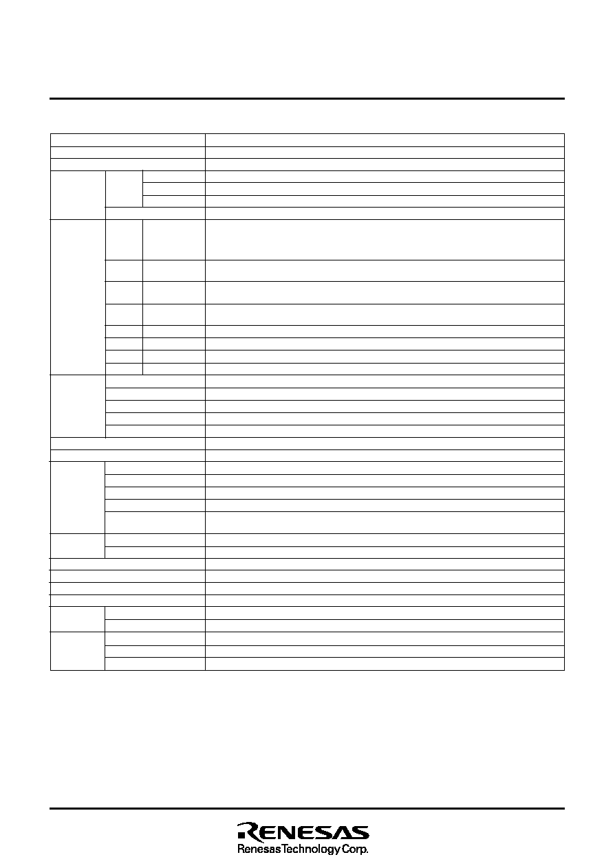
PERFORMANCE OVERVIEW
Function
159
0.5
µ
s (at 6 MHz oscillation frequency, in high-speed through mode)
8192 words
10 bits
12288 words
10 bits
16384 words
10 bits
512 words
4 bits (including LCD display RAM 20 words
4 bits)
Eight independent I/O ports.
Input is examined by skip decision.
The output structure can be switched by software.
Ports D
4
, D
5
, D
6
and D
7
are also used as S
IN
, S
OUT
, S
CK
and CNTR0 pin.
Two independent output ports.
Ports D
8
and D
9
are also used as INT0 and INT1, respectively.
4-bit I/O port; A pull-up function, a key-on wakeup function and output structure can be switched
by software.
4-bit I/O port; A pull-up function, a key-on wakeup function and output structure can be switched
by software.
4-bit I/O port; Ports P2
0
≠P2
3
are also used as A
IN0
≠A
IN3
, respectively.
4-bit I/O port; Ports P3
0
≠P3
3
are also used as A
IN4
≠A
IN7
, respectively.
4-bit I/O port; The output structure can be switched by software.
1-bit output; Port C is also used as CNTR1 pin.
8-bit programmable timer with a reload register and has an event counter.
8-bit programmable timer with a reload register.
8-bit programmable timer with a reload register and has an event counter.
8-bit programmable timer with two reload registers.
16-bit timer, fixed dividing frequency
10-bit
1, 8-bit comparator is equipped.
8-bit
1
1/2, 1/3 bias
2, 3, 4 duty
4
20
2r
3, 2r
2, r
3, r
2 (they can be switched by software.)
9 (two for external, five for timer, A-D, serial I/O)
1 level
8 levels
CMOS silicon gate
64-pin plastic molded QFP (64P6N)
≠20 ∞C to 85 ∞C
2 to 5.5 V (It depends on the operation source clock, operation mode and oscillation frequency.)
2.5 to 5.5 V (It depends on the operation source clock, operation mode and oscillation frequency.)
2.8 mA (at room temperature, V
DD
= 5 V, f(X
IN
) = 6 MHz, f(X
CIN
) = 32 kHz, f(STCK) = f(X
IN
))
20
µ
A (at room temperature, V
DD
= 5 V, f(X
CIN
) = 32 kHz)
0.1
µ
A (at room temperature, V
DD
= 5 V)
Parameter
Number of basic instructions
Minimum instruction execution time
Memory sizes
Input/Output
ports
Timers
A-D converter
Serial I/O
LCD control
circuit
Interrupt
Subroutine nesting
Device structure
Package
Operating temperature range
Supply
voltage
Power
dissipation
ROM
RAM
D
0
≠D
7
D
8
, D
9
P0
0
≠P0
3
P1
0
≠P1
3
P2
0
≠P2
3
P3
0
≠P3
3
P4
0
≠P4
3
C
Timer 1
Timer 2
Timer 3
Timer 4
Timer 5
Selective bias value
Selective duty value
Common output
Segment output
Internal resistor for
power supply
Sources
Nesting
Mask ROM version
One Time PROM version
Active mode
Clock operating mode
At RAM back-up
M34524M8
M34524MC
M34524ED
I/O
Output
I/O
I/O
I/O
I/O
I/O
Output