 | –≠–ª–µ–∫—Ç—Ä–æ–Ω–Ω—ã–π –∫–æ–º–ø–æ–Ω–µ–Ω—Ç: M34554MC | –°–∫–∞—á–∞—Ç—å:  PDF PDF  ZIP ZIP |
Document Outline
- ˛ˇ
- ˛ˇ
- ˛ˇ
- ˛ˇ
- Block diagram
- ˛ˇ
- ˛ˇ
- ˛ˇ
- ˛ˇ
- PROGRAM MEMORY (ROM)
- ˛ˇ
- ˛ˇ
- ˛ˇ
- ˛ˇ
- ˛ˇ
- ˛ˇ
- ˛ˇ
- ˛ˇ
- ˛ˇ
- ˛ˇ
- ˛ˇ
- ˛ˇ
- ˛ˇ
- ˛ˇ
- ˛ˇ
- ˛ˇ
- ˛ˇ
- ˛ˇ
- ˛ˇ
- ˛ˇ
- ˛ˇ
- ˛ˇ
- ˛ˇ
- ˛ˇ
- ˛ˇ
- ˛ˇ
- ˛ˇ
- ˛ˇ
- ˛ˇ
- ˛ˇ
- ˛ˇ
- ˛ˇ
- ˛ˇ
- ˛ˇ
- ˛ˇ
- ˛ˇ
- ˛ˇ
- ˛ˇ
- ˛ˇ
- ˛ˇ
- ˛ˇ
- ˛ˇ
- ˛ˇ
- ˛ˇ
- ˛ˇ
DESCRIPTION
The 4554 Group is a 4-bit single-chip microcomputer designed with
CMOS technology. Its CPU is that of the 4500 series using a
simple, high-speed instruction set. The computer is equipped with
main clock selection function, four 8-bit timers (each timer has one
or two reload register), interrupts, and LCD control circuit.
The various microcomputers in the 4554 Group include variations
of the built-in memory size as shown in the table below.
FEATURES
Minimum instruction execution time .................................. 0.5
µ
s
(at 6 MHz oscillation frequency, in high-speed through-mode)
Supply voltage
Mask ROM version ...................................................... 2.0 to 5.5 V
One Time PROM version ............................................. 2.5 to 5.5 V
(It depends on oscillation frequency and operation mode)
Timers
Timer 1 ...................................... 8-bit timer with a reload register
Timer 2 ...................................... 8-bit timer with a reload register
Timer 3 ...................................... 8-bit timer with a reload register
Timer 4 ................................. 8-bit timer with two reload registers
Timer 5 .............................. 16-bit timer (fixed dividing frequency)
Part number
M34554M8-XXXFP
M34554MC-XXXFP
M34554EDFP (Note)
ROM type
Mask ROM
Mask ROM
One Time PROM
Package
64P6N-A
64P6N-A
64P6N-A
RAM size
(
4 bits)
512 words
512 words
512 words
ROM (PROM) size
(
10 bits)
8192 words
12288 words
16384 words
Interrupt ........................................................................ 7 sources
Key-on wakeup function pins ................................................... 10
LCD control circuit
Segment output ........................................................................ 32
Common output .......................................................................... 4
Voltage drop detection circuit (Reset) ......................... Typ. 1.5 V
Watchdog timer
Clock generating circuit
Main clock
(ceramic resonator/RC oscillation/internal ring oscillator)
Sub-clock
(quartz-crystal oscillation)
LED drive directly enabled (port D)
APPLICATION
Remot control transmitter
Note: Shipped in blank.
Rev.2.00 Jul 01, 2003 page 1 of 136
4554 Group
SINGLE-CHIP 4-BIT CMOS MICROCOMPUTER
REJ03B0043-0200Z
Rev.2.00
Jul 01, 2003
Rev.2.00 Jul 01, 2003 page 2 of 136
4554 Group
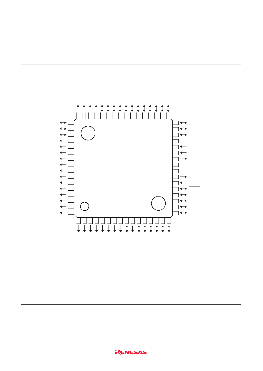
PIN CONFIGURATION
Pin configuration (top view) (4554 Group)
OUTLINE 64P6N-A
49
50
51
52
53
54
55
56
57
58
59
60
61
62
63
64
SEG
0
/V
LC3
SEG
1
/V
LC2
SEG
2
/V
LC1
SEG
3
SEG
4
SEG
5
SEG
6
M34554Mx-XXXFP
M34554EDFP
SEG
7
SEG
8
SEG
9
SEG
10
SEG
11
SEG
12
SEG
13
SEG
14
SEG
15
D
4
D
5
D
6
CNV
SS
VDCE
X
CIN
X
COUT
V
DD
V
SS
X
OUT
X
IN
RESET
D
7
/CNTR0
C/CNTR1
D
8
/INT0
D
9
/INT1
COM
0
COM
1
COM
2
COM
3
P0
0
P0
1
P0
2
P0
3
P1
0
P1
1
P1
2
P1
3
D
0
D
1
D
2
D
3
SEG
16
SEG
17
SEG
18
SEG
19
SEG
20
SEG
21
SEG
22
SEG
23
S
EG
24
/P3
3
S
EG
25
/P3
2
S
EG
26
/P3
1
S
EG
27
/P3
0
S
EG
28
/P2
3
S
EG
29
/P2
2
S
EG
30
/P2
1
S
EG
31
/P2
0
32
31
30
29
28
27
26
25
24
23
22
21
20
19
18
17
48 47 46 45 44 43 42 41 40 39 38 37 36 35 34 33
1
2
3
4
5
6
7
8
9
10 11 12 13 14 15 16

Rev.2.00 Jul 01, 2003 page 3 of 136
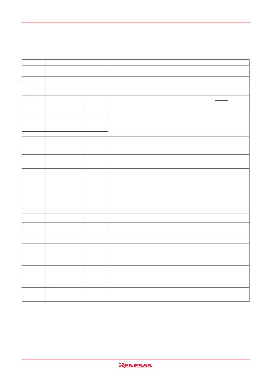
4554 Group
Block diagram (4554 Group)
R
A
M
R
O
M
M
e
m
o
r
y
I
/
O
p
o
r
t
I
n
t
e
r
n
a
l
p
e
r
i
p
h
e
r
a
l
f
u
n
c
t
i
o
n
s
T
i
m
e
r
T
i
m
e
r
1
(
8
b
i
t
s
)
S
y
s
t
e
m
c
l
o
c
k
g
e
n
e
r
a
t
i
o
n
c
i
r
c
u
i
t
T
i
m
e
r
2
(
8
b
i
t
s
)
5
1
2
w
o
r
d
s
4
b
i
t
s
L
C
D
d
i
s
p
l
a
y
R
A
M
i
n
c
l
u
d
i
n
g
3
2
w
o
r
d
s
4
b
i
t
s
8
1
9
2
,
1
2
2
8
8
,
1
6
3
8
4
w
o
r
d
s
1
0
b
i
t
s
4
5
0
0
s
e
r
i
e
s
C
P
U
c
o
r
e
R
e
g
i
s
t
e
r
B
(
4
b
i
t
s
)
R
e
g
i
s
t
e
r
A
(
4
b
i
t
s
)
R
e
g
i
s
t
e
r
D
(
3
b
i
t
s
)
R
e
g
i
s
t
e
r
E
(
8
b
i
t
s
)
S
t
a
c
k
r
e
g
i
s
t
e
r
S
K
(
8
l
e
v
e
l
s
)
I
n
t
e
r
r
u
p
t
s
t
a
c
k
r
e
g
i
s
t
e
r
S
D
P
(
1
l
e
v
e
l
)
A
L
U
(
4
b
i
t
s
)
W
a
t
c
h
d
o
g
t
i
m
e
r
(
1
6
b
i
t
s
)
P
o
r
t
P
0
4
P
o
r
t
P
1
4
P
o
r
t
P
2
4
P
o
w
e
r
-
o
n
r
e
s
e
t
c
i
r
c
u
i
t
V
o
l
t
a
g
e
d
r
o
p
d
e
t
e
c
t
i
o
n
c
i
r
c
u
i
t
T
i
m
e
r
3
(
8
b
i
t
s
)
T
i
m
e
r
4
(
8
b
i
t
s
)
L
C
D
d
r
i
v
e
c
o
n
t
r
o
l
c
i
r
c
u
i
t
(
M
a
x
.
3
2
s
e
g
m
e
n
t
s
4
c
o
m
m
o
n
)
X
I
N
-
X
O
U
T
(
M
a
i
n
c
l
o
c
k
)
X
C
I
N
-
X
C
O
U
T
(
S
u
b
-
c
l
o
c
k
)
S
e
g
m
e
n
t
o
u
t
p
u
t
3
2
C
o
m
m
o
n
o
u
t
p
u
t
4
P
o
r
t
P
3
4
P
o
r
t
D
8
T
i
m
e
r
5
(
1
6
b
i
t
s
)
P
o
r
t
C
1
2

Rev.2.00 Jul 01, 2003 page 4 of 136
4554 Group
PERFORMANCE OVERVIEW
Function
136
0.5
µ
s (at 6 MHz oscillation frequency, in high-speed through mode)
8192 words
10 bits
12288 words
10 bits
16384 words
10 bits
512 words
4 bits (including LCD display RAM 32 words
4 bits)
Eight independent I/O ports.
Input is examined by skip decision.
The output structure can be switched by software.
Port D
7
is also used as CNTR0 pin.
Two independent output ports.
Ports D
8
and D
9
are also used as INT0 and INT1, respectively.
4-bit I/O port; A pull-up function, a key-on wakeup function and output structure can be switched
by software.
4-bit I/O port; A pull-up function, a key-on wakeup function and output structure can be switched
by software.
4-bit input port; Port P2
0
≠P2
3
are also used as SEG
31
≠SEG
28
pins.
4-bit input port; Port P3
0
≠P3
3
are also used as SEG
27
≠SEG
24
pins.
1-bit output; Port C is also used as CNTR1 pin.
8-bit programmable timer with a reload register and has an event counter.
8-bit programmable timer with a reload register.
8-bit programmable timer with a reload register and has an event counter.
8-bit programmable timer with two reload registers.
16-bit timer, fixed dividing frequency
1/2, 1/3 bias
2, 3, 4 duty
4
32
2r
3, 2r
2, r
3, r
2 (they can be switched by software.)
7 (two for external, five for timer)
1 level
8 levels
CMOS silicon gate
64-pin plastic molded QFP (64P6N)
≠20 ∞C to 85 ∞C
2 to 5.5 V (It depends on the operation source clock, operation mode and oscillation frequency.)
2.5 to 5.5 V (It depends on the operation source clock, operation mode and oscillation frequency.)
2.8 mA (at room temperature, V
DD
= 5 V, f(X
IN
) = 6 MHz, f(X
CIN
) = 32 kHz, f(STCK) = f(X
IN
))
20
µ
A (at room temperature, V
DD
= 5 V, f(X
CIN
) = 32 kHz)
0.1
µ
A (at room temperature, V
DD
= 5 V)
Parameter
Number of basic instructions
Minimum instruction execution time
Memory sizes
Input/Output
ports
Timers
LCD control
circuit
Interrupt
Subroutine nesting
Device structure
Package
Operating temperature range
Supply
voltage
Power
dissipation
ROM
RAM
D
0
≠D
7
D
8
, D
9
P0
0
≠P0
3
P1
0
≠P1
3
P2
0
≠P2
3
P3
0
≠P3
3
C
Timer 1
Timer 2
Timer 3
Timer 4
Timer 5
Selective bias value
Selective duty value
Common output
Segment output
Internal resistor for
power supply
Sources
Nesting
Mask ROM version
One Time PROM version
Active mode
Clock operating mode
At RAM back-up
M34554M8
M34554MC
M34554ED
I/O
Output
I/O
I/O
Input
Input
Output
Rev.2.00 Jul 01, 2003 page 5 of 136
4554 Group
PIN DESCRIPTION
Name
Power supply
Ground
CNV
SS
Voltage drop
detection circuit
enable
Reset input/output
Main clock input
Sub-clock input
Sub-clock output
Pin
V
DD
V
SS
CNV
SS
VDCE
RESET
X
IN
X
CIN
X
COUT
Input/Output
--
--
--
Input
I/O
Input
Input
Output
Function
Connected to a plus power supply.
Connected to a 0 V power supply.
Connect CNV
SS
to V
SS
and apply "L" (0V) to CNV
SS
certainly.
This pin is used to operate/stop the voltage drop detection circuit. When "H" level is
input to this pin, the circuit starts operating. When "L" level is input to this pin, the
circuit stops operating.
An N-channel open-drain I/O pin for a system reset. When the watchdog timer or the
voltage drop detection circuit cause the system to be reset, the RESET pin outputs
"L" level.
I/O pins of the main clock generating circuit. When using a ceramic resonator, con-
nect it between pins X
IN
and X
OUT
. A feedback resistor is built-in between them.
When using the RC oscillation, connect a resistor and a capacitor to X
IN
, and leave
X
OUT
pin open.
I/O pins of the sub-clock generating circuit. Connect a 32 kHz quartz-crystal oscillator
between pins X
CIN
and X
COUT
. A feedback resistor is built-in between them.
X
OUT
Main clock output
Output
D
0
≠D
7
D
8
, D
9
P0
0
≠P0
3
P1
0
≠P1
3
P2
0
≠P2
3
P3
0
≠P3
3
Port C
COM
0
≠
COM
3
SEG
0
≠SEG
31
V
LC3
≠V
LC1
CNTR0,
CNTR1
INT0, INT1
I/O port D
Input is examined by
skip decision.
Output port D
I/O port P0
I/O port P1
Input port P2
Input port P3
Output port C
Common output
Segment output
LCD power supply
Timer input/output
Interrupt input
I/O
Output
I/O
I/O
Input
Input
Output
Output
Output
≠
I/O
Input
Each pin of port D has an independent 1-bit wide I/O function. The output structure
can be switched to N-channel open-drain or CMOS by software. For input use, set
the latch of the specified bit to "1" and select the N-channel open-drain. Port D
7
is
also used as CNTR0 pin.
Each pin of port D has an independent 1-bit wide output function. The output struc-
ture is N-channel open-drain. Ports D
8
and D
9
are also used as INT0 pin and INT1
pin, respectively.
P
ort P0 serves as a 4-bit I/O port. The output structure can be switched to N-channel
open-drain or CMOS by software. For input use, set the latch of the specified bit to
"1" and select the N-channel open-drain. Port P0 has a key-on wakeup function and
a pull-up function. Both functions can be switched by software.
P
ort P1 serves as a 4-bit I/O port. The output structure can be switched to N-channel
open-drain or CMOS by software. For input use, set the latch of the specified bit to
"1" and select the N-channel open-drain. Port P1 has a key-on wakeup function and
a pull-up function. Both functions can be switched by software.
P
ort P2 serves as a 4-bit input port.
Ports P2
0
≠P2
3
are also used as SEG
31
≠SEG
28
, respectively.
P
ort P3 serves as a 4-bit input port.
Ports P3
0
≠P3
3
are also used as SEG
27
≠SEG
24
, respectively.
1
-bit output port. The output structure is CMOS. Port C is also used as CNTR1 pin.
LCD common output pins. Pins COM
0
and COM
1
are used at 1/2 duty, pins COM
0
≠
COM
2
are used at 1/3 duty and pins COM
0
≠COM
3
are used at 1/4 duty.
LCD segment output pins. SEG
0
≠SEG
2
pins are used as V
LC3
≠V
LC1
pins, respectively.
LCD power supply pins.
When the internal resistor is used, V
DD
pin is connected to V
LC3
pin (if luminance ad-
justment is required, V
DD
pin is connected to V
LC3
pin through a resistor).
When the external power supply is used, apply the voltage 0
V
LC1
V
LC2
V
LC3
V
DD
.
V
LC3
≠V
LC1
pins are used as SEG
0
≠SEG
2
pins, respectively.
CNTR0 pin has the function to input the clock for the timer 1 event counter, and to
output the timer 1 or timer 2 underflow signal divided by 2.
CNTR1 pin has the function to input the clock for the timer 3 event counter, and to
output the PWM signal generated by timer 4.CNTR0 pin and CNTR1 pin are also
used as Ports D
7
and C, respectively.
INT0 pin and INT1 pin accept external interrupts. They have the key-on wakeup func-
tion which can be switched by software. INT0 pin and INT1 pin are also used as
Ports D
8
and D
9
, respectively.