ChipFind - документация

Электронный компонент: M37540M2

Скачать:  PDF   ZIP

Document Outline

DESCRIPTION
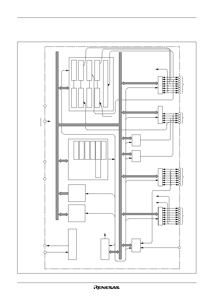
The 7540 Group is the 8-bit microcomputer based on the 740 fam-
ily core technology.
The 7540 Group has a serial I/O, 8-bit timers, a 16-bit timer, and
an A-D converter, and is useful for control of home electric appli-
ances and office automation equipment.
FEATURES
Basic machine-language instructions ...................................... 71
The minimum instruction execution time ......................... 0.34
s
(at 6 MHz oscillation frequency, double-speed mode for the
shortest instruction)
Memory size ROM ............................................ 8 K to 32 K bytes
RAM ............................................. 384 to 768 bytes
Programmable I/O ports ....................... 29 (25 in 32-pin version)
Interrupts ................................................. 15 sources, 15 vectors
................................. (14 sources, 14 vectors for 32-pin version)
Timers ............................................................................. 8-bit
4
...................................................................................... 16-bit
1
Serial I/O1 ................... 8-bit
1 (UART or Clock-synchronized)
Serial I/O2 (Note 1) ..................... 8-bit
1
(Clock-synchronized)
A-D converter ............................................... 10-bit
8 channels
.................................................... (6 channels for 32-pin version)
Clock generating circuit ............................................. Built-in type
(low-power dissipation by a ring oscillator enabled)
(connect to external ceramic resonator or quartz-crystal oscilla-
tor permitting RC oscillation)
Watchdog timer ............................................................ 16-bit
1
Power source voltage
X
IN
oscillation frequency at ceramic oscillation, in double-speed mode
At 6 MHz .................................................................... 4.5 to 5.5 V
X
IN
oscillation frequency at ceramic oscillation, in high-speed mode
At 8 MHz .................................................................... 4.0 to 5.5 V
At 4 MHz .................................................................... 2.4 to 5.5 V
At 2 MHz .................................................................... 2.2 to 5.5 V
X
IN
oscillation frequency at RC oscillation in high-speed mode or
middle-speed mode
At 4 MHz .................................................................... 4.0 to 5.5 V
At 2 MHz .................................................................... 2.4 to 5.5 V
At 1 MHz .................................................................... 2.2 to 5.5 V
Power dissipation
Mask ROM version ....................................... 22.5 mW (standard)
One Time PROM version ................................ 30 mW (standard)
Operating temperature range ................................... 20 to 85 C
(40 to 85 C for extended operating temperature version)
(40 to 125 C for extended operating temperature 125 C ver-
sion (Note 2))
APPLICATION
Office automation equipment, factory automation equipment,
home electric appliances, consumer electronics, car, etc.
Notes 1: Serial I/O2 can be used in the following cases;
(1) Serial I/O1 is not used,
(2) Serial I/O1 is used as UART and BRG output divided by 16 is
selected as the synchronized clock.
2: In this version, the operating temperature range and total time
are limited as follows;
55 C to 85 C: within total 6000 hours,
85 C to 125 C: within total 1000 hours.
PRELIMINARY
Notice: This is not a final specification.
Some parametric limits are subject to change.
Rev.3.20 2003.05.28 page 1 of 83
7540 Group
SINGLE-CHIP 8-BIT CMOS MICROCOMPUTER
REJ03B0011-0320Z
Rev.3.20
2003.05.28
Rev.3.20 2003.05.28 page 2 of 83
7540 Group
PRELIMINARY
Notice: This is not a final specification.
Some parametric limits are subject to change.
Fig. 2 Pin configuration (36P2R-A type)
Package type: 36P2R-A
10
1
2
3
4
6
7
8
9
11
12
14
15
16
5
13
17
18
36
35
34
33
31
30
26
25
24
23
22
21
20
19
32
27
29
28
P0
0
/CNTR
1
CNV
SS
X
OUT
X
IN
V
SS
P0
1
/TY
OUT
P0
2
/TZ
OUT
P0
3
/TX
OUT
P0
4
P3
0
(LED
0
)
Vcc
V
REF
P0
5
P1
0
/R
X
D
1
P2
6
/AN
6
P2
7
/AN
7
P1
1
/T
X
D
1
P1
2
/S
CLK1
/S
CLK2
P1
3
/S
RDY1
/S
DATA2
P2
3
/AN
3
P2
2
/AN
2
P2
1
/AN
1
P2
0
/AN
0
P3
1
(LED
1
)
P3
6
(LED
6
)/INT
1
P2
4
/AN
4
P2
5
/AN
5
P0
6
P0
7
P3
7
/INT
0
RESET
M37540Mx-XXXFP
M37540MxT-XXXFP
M37540MxV-XXXFP
M37540E8FP
M37540E8T-XXXFP
M37540E8V-XXXFP
P1
4
/CNTR
0
P3
5
(LED
5
)
P3
4
(LED
4
)
P3
3
(LED
3
)
P3
2
(LED
2
)
PIN CONFIGURATION (TOP VIEW)
Fig. 1 Pin configuration (32P6U-A type)
Package type: 32P6U-A
P0
7
P1
0
/R
X
D
1
P1
1
/T
X
D
1
P1
2
/S
CLK1
/S
CLK2
P1
3
/S
RDY1
/S
DATA2
P1
4
/CNTR
0
P2
0
/
AN
0
P2
1
/
AN
1
32
31
30
29
28
27
26
25
P3
4
(LED
4
)
P3
3
(LED
3
)
P3
2
(LED
2
)
P3
1
(LED
1
)
P3
0
(LED
0
)
V
SS
X
OUT
X
IN
9
10
11
12
13
14
15
16
2
8
7
6
5
3
1
4
V
CC
CNV
SS
RESET
P2
2
/AN
2
P0
5
20
17
18
19
21
24
P0
2
/TZ
OUT
P0
4
P0
3
/TX
OUT
P0
6
23
22
P0
1
/TY
OUT
P0
0
/CNTR
1
P3
7
/INT
0
M37540Mx-XXXGP
M37540MxT-XXXGP
M37540MxV-XXXGP
M37540ExGP
M37540E8T-XXXGP
M37540E8V-XXXGP
P2
3
/AN
3
P2
4
/AN
4
P2
5
/AN
5
V
REF
Rev.3.20 2003.05.28 page 3 of 83
7540 Group
PRELIMINARY
Notice: This is not a final specification.
Some parametric limits are subject to change.
Fig. 4 Pin configuration (42S1M type)
Outline 42S1M
10
1
2
3
4
6
7
8
9
11
12
14
15
16
5
13
17
18
36
35
34
33
31
30
26
25
24
23
22
32
27
29
28
19
20
21
42
41
40
39
37
38
P0
0
/CNTR
1
CNV
SS
X
OUT
X
IN
V
SS
P0
1
/TY
OUT
P0
2
/TZ
OUT
P0
3
/TX
OUT
P0
4
P3
0
(LED
0
)
Vcc
V
REF
P0
5
P1
2
/S
CLK1
/S
CLK2
P2
5
/AN
5
P2
6
/AN
6
P1
3
/S
RDY1
/S
DATA2
P1
4
/CNTR
0
NC
P2
2
/AN
2
NC
P2
1
/AN
1
P2
0
/AN
0
P3
1
(LED
1
)
P3
6
(LED
6
)/INT
1
P2
3
/AN
3
P2
4
/AN
4
P0
6
P0
7
P3
7
/INT
0
RESET
M37540RSS
NC
P3
5
(LED
5
)
P3
4
(LED
4
)
P3
3
(LED
3
)
P3
2
(LED
2
)
NC
P1
0
/R
X
D
1
P1
1
/T
X
D
1
NC
NC
P2
7
/AN
7
Fig. 3 Pin configuration (32P4B-A type)
1
2
3
4
5
6
7
8
9
10
11
12
13
14
15
16
CNV
SS
P1
2
/S
CLK1
/S
CLK2
P1
3
/S
RDY1
/S
DATA2
P1
4
/CNTR
0
P2
0
/AN
0
P2
1
/AN
1
P2
2
/AN
2
P2
3
/AN
3
P2
4
/AN
4
V
CC
X
IN
X
OUT
V
SS
P1
1
/T
X
D
1
P1
0
/R
X
D
1
P0
7
P0
6
P0
5
P0
4
P3
0
(LED
0
)
P2
5
/AN
5
V
REF
RESET
P0
0
/CNTR
1
P3
3
(LED
3
)
P3
2
(LED
2
)
P3
1
(LED
1
)
M37540Mx-XXXSP
M37540ExSP
32
P0
1
/TY
OUT
P0
2
/TZ
OUT
P0
3
/TX
OUT
14
15
16
P3
7
/INT
0
P3
4
(LED
4
)
17
18
19
20
21
22
23
24
25
26
27
28
29
30
31
Package type: 32P4B
Rev.3.20 2003.05.28 page 4 of 83
7540 Group
PRELIMINARY
Notice: This is not a final specification.
Some parametric limits are subject to change.
FUNCTIONAL BLOCK
Fig. 5 Functional block diagram (32P6U package)
FUNCTIONAL BLOCK DIAGRAM (Package: 32P6U)
X
IN
OUT
X
SI/O1(8)
RAM
ROM
CPU
A
X
Y
S
PC
H
PC
L
PS
V
SS
11
RESET
6
V
CC
8
7
CNV
SS
P1(5)
30
28
26
29
27
32
31
P2(6)
P3(6)
12
15
13
5
Reset input
I/O port P2
I/O port P1
I/O port P3
Clock generating circuit
Clock input
Clock output
9
10
4
2
3
1
A-D
converter
(10)
V
REF
Watchdog timer
Reset
0
14
INT
0
16
17
SI/O2(8)
CNTR
0
I/O port P0
Prescaler Y (8)
Prescaler Z (8)
Timer X (8)
Timer Z (8)
Timer Y (8)
Key-on wakeup
TY
OUT
TZ
OUT
Prescaler X (8)
CNTR
1
Timer A (16)
P0(8)
25
23
21
19
24
22
20
18
INT
0
Timer 1 (8)
Prescaler 1 (8)
TX
OUT
Rev.3.20 2003.05.28 page 5 of 83
7540 Group
PRELIMINARY
Notice: This is not a final specification.
Some parametric limits are subject to change.
Fig. 6 Functional block diagram (36P2R package)
FUNCTIONAL BLOCK DIAGRAM (Package: 36P2R)
A-D
converter
(10)
X
IN
OUT
X
CPU
V
SS
18
RESET
13
V
CC
15
14
CNV
SS
P0(8)
34
32
30
28
33
31
29
27
P1(5)
31
35
2
36
7
5
6
4
P2(8)
P3(8)
20
23
21
19
12
I/O port P2
I/O port P0
I/O port P1
I/O port P3
16
17
11
9
10
8
0
22
26
24
25
SI/O1(8)
RAM
ROM
A
X
Y
S
PC
H
PC
L
PS
Reset input
Clock generating circuit
Clock input
Clock output
V
REF
Watchdog timer
Reset
INT
0
SI/O2(8)
CNTR
0
Prescaler Y (8)
Prescaler Z (8)
Timer X (8)
Timer Z (8)
Timer Y (8)
Key-on wakeup
TY
OUT
TZ
OUT
Prescaler X (8)
CNTR
1
Timer A (16)
INT
0
Timer 1 (8)
Prescaler 1 (8)
TX
OUT
INT
1