ChipFind - документация

Электронный компонент: M37542M4V

Скачать:  PDF   ZIP

Document Outline

DESCRIPTION
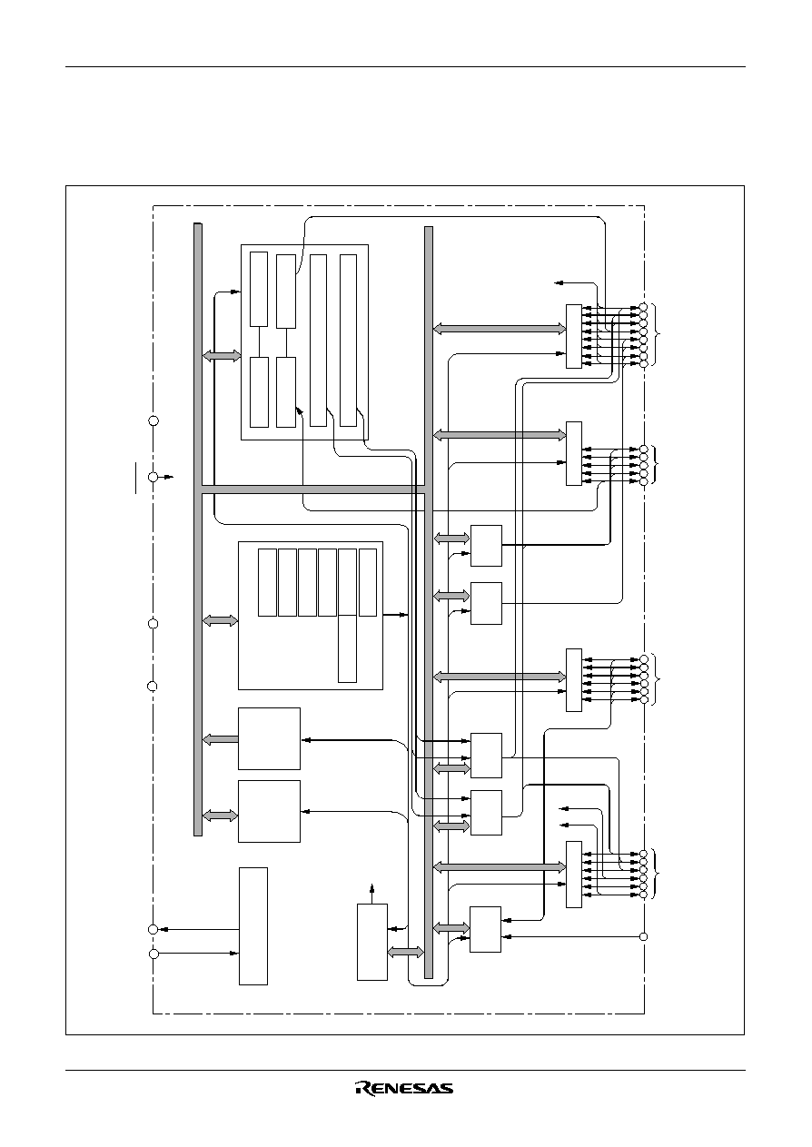
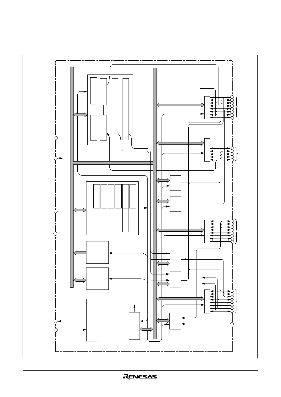
The 7542 Group is the 8-bit microcomputer based on the 740 fam-
ily core technology.
The 7542 Group has serial I/Os, 8-bit timers, 16-bit timers, and an
A-D converter, and is useful for control of home electric appliances
and office automation equipment.
FEATURES
Basic machine-language instructions ...................................... 71
The minimum instruction execution time ..
0.25


s (Target Spec.)
(at 8 MHz oscillation frequency, double-speed mode for the
shortest instruction)
Memory size
Flash memory version: ROM .............................. 32K + 4K bytes
RAM ..................................... 1024 bytes
Mask ROM version:
ROM ............................. 8K to 16K bytes
RAM ............................ 384 to 512 bytes
RSS version
RAM ..................................... 1024 bytes
Programmable I/O ports ....................... 29 (25 in 32-pin version)
Interrupts ................................................. 18 sources, 16 vectors
(14 sources, 14 vectors in 32-pin version)
Timers ............................................................................. 8-bit
2
...................................................................................... 16-bit
2
Output compare ............................................................ 4-channel
Input capture ................................................................ 2-channel
Serial I/O ...................... 8-bit
2 (UART or Clock-synchronized)
A-D converter ............................................... 10-bit
8 channels
...................................................... (6 channels in 32-pin version)
Clock generating circuit ............................................. Built-in type
(low-power dissipation by a ring oscillator)
(connected to external ceramic resonator or quartz-crystal
oscillator permitting RC oscillation)
PRELIMINARY
Notice: This is not a final specification.
Some parametric limits are subject to change.
Watchdog timer ............................................................ 16-bit
1
Power source voltage
X
IN
oscillation frequency at ceramic oscillation, in double-speed mode
At 8 MHz ................................................................................
TBD
X
IN
oscillation frequency at ceramic oscillation, in high-speed mode
At 8 MHz .................................................................... 4.0 to 5.5 V
At 4 MHz .................................................................... 2.4 to 5.5 V
At 2 MHz .................................................................... 2.2 to 5.5 V
X
IN
oscillation frequency at RC oscillation in high-speed mode or
middle-speed mode
At 4 MHz .................................................................... 4.0 to 5.5 V
At 2 MHz .................................................................... 2.4 to 5.5 V
At 1 MHz .................................................................... 2.2 to 5.5 V
Power dissipation ..................................................................
TBD
Operating temperature range ................................... 20 to 85 C
(40 to 85 C for extended operating temperature version)
(40 to 125 C for extended operating temperature 125 C ver-
sion (Note 1))
Notes 1: In this version, the operating temperature range and total time are
limited as follows;
55 C to 85 C: within total 6000 hours,
85 C to 125 C: within total 1000 hours.
2: This is not a final specification. Some parametric limits are subject
to change.Please contact Renesas or an authorized Renesas
product distributor in the case of examination of use.
APPLICATION
Office automation equipment, factory automation equipment, home
electric appliances, consumer electronics, car, etc.
Rev.2.00 2003.04.21 page 1 of 97
7542 Group
SINGLE-CHIP 8-BIT CMOS MICROCOMPUTER
REJ03B0006-0200Z
Rev.2.00
2003.04.21
Rev.2.00 2003.04.21 page 2 of 97
7542 Group
PRELIMINARY
Notice: This is not a final specification.
Some parametric limits are subject to change.
Fig. 2 Pin configuration (Package type: 36P2R-A)
PIN CONFIGURATION (TOP VIEW)
Fig. 1 Pin configuration (Package type: 32P6U-A)
Package type: 32P6U-A
P0
7
(LED
07
)/S
RDY2
P1
0
/R
X
D
1
/CAP
0
P1
1
/T
X
D
1
P1
2
/S
CLK1
P1
3
/S
RDY1
P1
4
/CNTR
0
P2
0
/
AN
0
P2
1
/
AN
1
32
31
30
29
28
27
26
25
P3
4
(LED
14
)
P3
3
(LED
13
)/INT
1
P3
2
(LED
12
)/CMP
3
P3
1
(LED
11
)/CMP
2
P3
0
(LED
10
)/CAP
1
V
SS
X
OUT
X
IN
9
10
11
12
13
14
15
16
8
7
6
5
3
1
4
V
CC
CNV
SS
RESET
P2
2
/AN
2
P0
5
(LED
05
)/TxD
2
20
17
18
19
21
24
P0
2
(LED
02
)/CMP
1
P0
4
(LED
04
)/RxD
2
P0
3
(LED
03
)/TX
OUT
P0
6
(LED
06
)/S
CLK2
23 22
P0
1
(LED
01
)/CMP
0
P0
0
(LED
00
)/CAP
0
P3
7
(LED
17
)/INT
0
M37542Mx-XXXGP
M37542MxT-XXXGP
M37542MxV-XXXGP
M37542F8GP
M37542F8TGP
M37542F8VGP
P2
3
/AN
3
P2
4
/AN
4
P2
5
/AN
5
V
REF
2
Package type: 36P2R-A
10
1
2
3
4
6
7
8
9
11
12
14
15
16
5
13
17
18
36
35
34
33
31
30
26
25
24
23
22
21
20
19
32
27
29
28
CNV
SS
X
OUT
X
IN
V
SS
P0
4
(LED
04
)/RxD
2
P3
0
(LED
10
)/CAP
1
Vcc
V
REF
P0
5
(LED
05
)/TxD
2
P1
0
/R
X
D
1
/CAP
0
P2
6
/AN
6
P2
7
/AN
7
P1
1
/T
X
D
1
P1
2
/S
CLK1
P1
3
/S
RDY1
P2
3
/AN
3
P2
2
/AN
2
P2
1
/AN
1
P2
0
/AN
0
P3
1
(LED
11
)/CMP
2
P3
6
(LED
16
)/INT
1
P2
4
/AN
4
P2
5
/AN
5
P0
6
(LED
06
)/S
CLK2
P0
7
(LED
07
)/S
RDY2
RESET
M37542Mx-XXXFP
M37542MxT-XXXFP
M37542MxV-XXXFP
M37542F8FP
M37542F8TFP
M37542F8VFP
P1
4
/CNTR
0
P3
5
(LED
15
)
P3
4
(LED
14
)
P3
3
(LED
13
)/INT
1
P3
2
(LED
12
)/CMP
3
P3
7
(LED
17
)/INT
0
P0
0
(LED
00
)/CAP
0
P0
1
(LED
01
)/CMP
0
P0
2
(LED
02
)/CMP
1
P0
3
(LED
03
)/TX
OUT
Rev.2.00 2003.04.21 page 3 of 97
7542 Group
PRELIMINARY
Notice: This is not a final specification.
Some parametric limits are subject to change.
Fig. 4 Pin configuration (Package type: 42S1M)
Fig. 3 Pin configuration (Package type: 32P4B)
1
2
3
4
5
6
7
8
9
10
11
12
13
14
15
16
CNV
SS
P1
2
/S
CLK1
P1
3
/S
RDY1
P1
4
/CNTR
0
P2
0
/AN
0
P2
1
/AN
1
P2
2
/AN
2
P2
3
/AN
3
P2
4
/AN
4
V
CC
X
IN
X
OUT
V
SS
P1
1
/T
X
D
1
P1
0
/R
X
D
1
/CAP
0
P0
7
(LED
07
)/S
RDY2
P0
6
(LED
06
)/S
CLK2
P0
5
(LED
05
)/TxD
2
P0
4
(LED
04
)/RxD
2
P3
0
(LED
10
)/CAP
1
P2
5
/AN
5
V
REF
RESET
P3
3
(LED
13
)/INT
1
P3
2
(LED
12
)/CMP
3
P3
1
(LED
11
)/CMP
2
M37542Mx-XXXSP
M37542F8SP
32
14
15
16
P3
4
(LED
14
)
17
18
19
20
21
22
23
24
25
26
27
28
29
30
31
Package type: 32P4B
P0
3
(LED
03
)/TX
OUT
P0
2
(LED
02
)/CMP
1
P0
1
(LED
01
)/CMP
0
P0
0
(LED
00
)/CAP
0
P3
7
(LED
17
)/INT
0
Package type 42S1M
10
1
2
3
4
6
7
8
9
11
12
14
15
16
5
13
17
18
36
35
34
33
31
30
26
25
24
23
22
32
27
29
28
19
20
21
42
41
40
39
37
38
CNV
SS
X
OUT
X
IN
V
SS
P0
4
(LED
04
)/RxD
2
P3
0
(LED
10
)/CAP
1
Vcc
V
REF
P0
5
(LED
05
)/TxD
2
P1
2
/S
CLK1
P2
5
/AN
5
P2
6
/AN
6
P1
3
/S
RDY1
P1
4
/CNTR
0
NC
P2
2
/AN
2
NC
P2
1
/AN
1
P2
0
/AN
0
P3
1
(LED
11
)/CMP
2
P3
6
(LED
16
)/INT
1
P2
3
/AN
3
P2
4
/AN
4
P0
6
(LED
06
)/S
CLK2
P0
7
(LED
07
)/S
RDY2
RESET
M37542RSS
NC
P3
5
(LED
15
)
P3
4
(LED
14
)
P3
3
(LED
13
)/INT
1
P3
2
(LED
12
)/CMP
3
NC
P1
0
/R
X
D
1
/CAP
0
P1
1
/T
X
D
1
NC
NC
P2
7
/AN
7
P3
7
(LED
17
)/INT
0
P0
0
(LED
00
)/CAP
0
P0
1
(LED
01
)/CMP
0
P0
2
(LED
02
)/CMP
1
P0
3
(LED
03
)/TX
OUT
Rev.2.00 2003.04.21 page 4 of 97
7542 Group
PRELIMINARY
Notice: This is not a final specification.
Some parametric limits are subject to change.
FUNCTIONAL BLOCK
Fig. 5 Functional block diagram (Package type: 32P6U-A)
FUNCTIONAL BLOCK DIAGRAM (Package type: 32P6U-A)
X
IN
OUT
X
SI/O2(8)
RAM
ROM
CPU
A
X
Y
S
PC
H
PC
L
PS
V
SS
11
RESET
6
V
CC
8
7
CNV
SS
P1(5)
30
28
26
29
27
32
31
P2(6)
P3(6)
12
15
13
5
Reset input
I/O port P2
I/O port P1
I/O port P3
Clock generating circuit
Clock input
Clock output
9
10
4
2
3
1
A-D
converter
(10)
V
REF
Watchdog timer
Reset
0
14
INT
0
16
17
SI/O1(8)
CNTR
0
I/O port P0
Timer X (8)
Key-on wakeup
Prescaler X (8)
Timer B (16)
P0(8)
25
23
21
19
24
22
20
18
Timer 1 (8)
Prescaler 1 (8)
Timer A (16)
Input
Capture
Output
Compare
INT
1
Rev.2.00 2003.04.21 page 5 of 97
7542 Group
PRELIMINARY
Notice: This is not a final specification.
Some parametric limits are subject to change.
Fig. 6 Functional block diagram (Package type: 36P2R-A)
FUNCTIONAL BLOCK DIAGRAM (Package type: 36P2R-A)
X
IN
OUT
X
SI/O2(8)
RAM
ROM
CPU
A
X
Y
S
PC
H
PC
L
PS
V
SS
18
RESET
13
V
CC
15
14
CNV
SS
P1(5)
31
35
2
36
76
P2(8)
P3(8)
21
24
22
12
Reset input
I/O port P2
I/O port P1
I/O port P3
Clock generating circuit
Clock input
Clock output
16
17
11
9
10
8
A-D
converter
(10)
V
REF
Watchdog timer
Reset
0
23
INT
0
25
26
SI/O1(8)
CNTR
0
I/O port P0
Timer X (8)
Key-on wakeup
Prescaler X (8)
Timer B (16)
P0(8)
34
32
30
28
33
31
29
27
Timer 1 (8)
Prescaler 1 (8)
Timer A (16)
INT
1
19
20
5
4
Input
Capture
Output
Compare