 | –≠–ª–µ–∫—Ç—Ä–æ–Ω–Ω—ã–π –∫–æ–º–ø–æ–Ω–µ–Ω—Ç: M37544M2 | –°–∫–∞—á–∞—Ç—å:  PDF PDF  ZIP ZIP |
Document Outline
- ˛ˇ
- ˛ˇ
- ˛ˇ
- ˛ˇ
- ˛ˇ
- ˛ˇ
- ˛ˇ
- ˛ˇ
- ˛ˇ
- ˛ˇ
- SFR
- ˛ˇ
- ˛ˇ
- ˛ˇ
- ˛ˇ
- ˛ˇ
- ˛ˇ
- ˛ˇ
- ˛ˇ
- ˛ˇ
- ˛ˇ
- ˛ˇ
- ˛ˇ
- ˛ˇ
- ˛ˇ
- ˛ˇ
DESCRIPTION
The 7544 Group is the 8-bit microcomputer based on the 740 fam-
ily core technology.
The 7544 Group has a serial I/O, 8-bit timers, a 16-bit timer, and
an A-D converter, and is useful for control of home electric appli-
ances and office automation equipment.
FEATURES
∑
Basic machine-language instructions ...................................... 71
∑
The minimum instruction execution time ......................... 0.25 µs
(at 8 MHz oscillation frequency, double-speed mode for the
shortest instruction)
∑
Memory size ROM ......................................................... 8 K bytes
RAM ........................................................ 256 bytes
∑
Programmable I/O ports ........................................................... 25
∑
Interrupts ................................................. 12 sources, 12 vectors
∑
Timers ............................................................................. 8-bit
2
...................................................................................... 16-bit
1
∑
Serial I/O ...................... 8-bit
1 (UART or Clock-synchronized)
∑
A-D converter ................................................. 8-bit
6 channels
∑
Clock generating circuit ............................................. Built-in type
(low-power dissipation by a ring oscillator enabled)
(connect to external ceramic resonator or quartz-crystal oscilla-
tor permitting RC oscillation)
∑
Watchdog timer ............................................................ 16-bit
1
∑
Power source voltage
X
IN
oscillation frequency at ceramic/quartz-crystal oscillation, in
double-speed mode
At 8 MHz .................................................................... 4.5 to 5.5 V
X
IN
oscillation frequency at ceramic/quartz-crystal oscillation, in
high-speed mode
At 8 MHz .................................................................... 4.0 to 5.5 V
X
IN
oscillation frequency at RC oscillation
At 4 MHz .................................................................... 4.0 to 5.5 V
∑
Power dissipation ........................................... 22.5mW(standard)
∑
Operating temperature range ................................... ≠20 to 85 ∞C
APPLICATION
Office automation equipment, factory automation equipment,
home electric appliances, consumer electronics, etc.
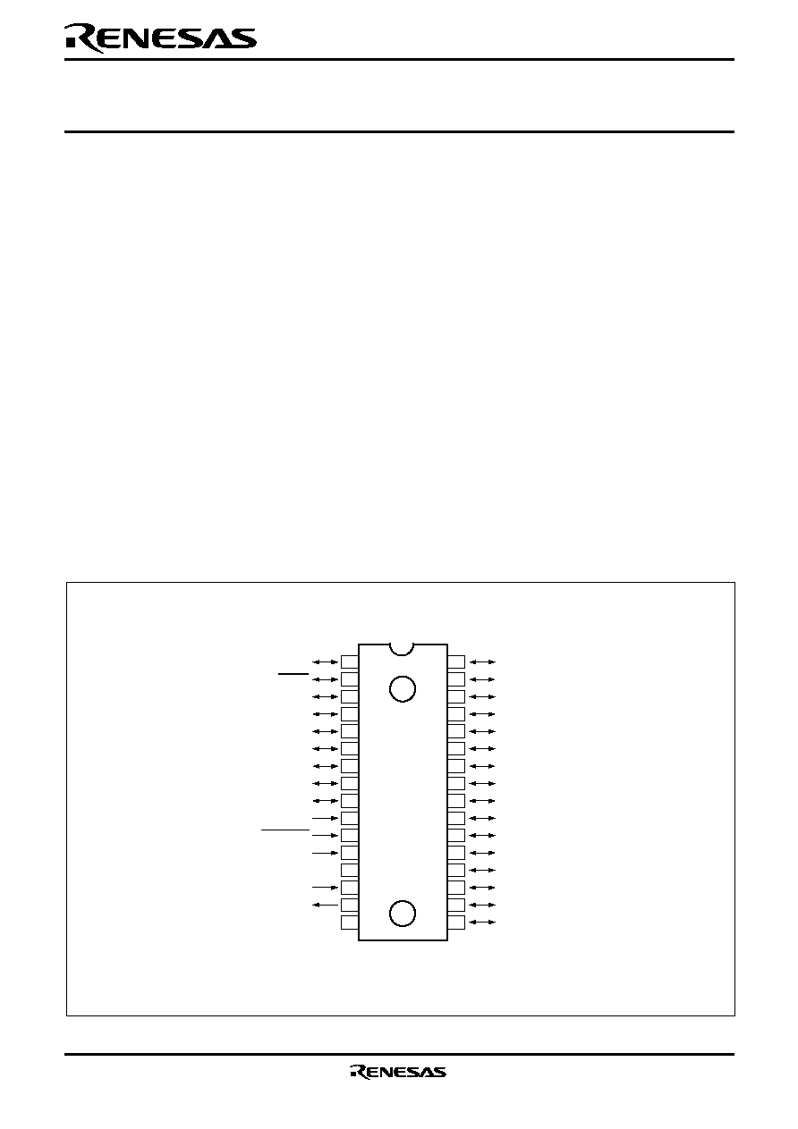
PIN CONFIGURATION (TOP VIEW)
Fig. 1 Pin configuration (32P4B type)
Package type : 32P4B
P1
2
/S
CLK
M37544M2-XXXSP
M37544G2SP
32
31
30
29
28
27
26
25
24
23
22
21
20
19
18
17
1
2
3
4
5
6
7
8
9
10
11
12
13
14
15
16
P1
3
/S
RDY
P1
4
/CNTR
0
P2
0
/AN
0
P2
1
/AN
1
P2
2
/AN
2
P2
3
/AN
3
P2
4
/AN
4
P2
5
/AN
5
V
REF
CNV
SS
V
CC
X
IN
X
OUT
V
SS
RESET
P1
1
/T
X
D
P1
0
/R
X
D
P0
7
(LED
7
)
P0
6
(LED
6
)
P0
5
(LED
5
)
P0
4
(LED
4
)
P0
3
(LED
3
)/TX
OUT
P0
2
(LED
2
)
P0
1
(LED
1
)
P0
0
(LED
0
)/CNTR
1
P3
4
(LED
12
)/INT
1
P3
3
(LED
11
)
P3
2
(LED
10
)
P3
1
(LED
9
)
P3
0
(LED
8
)
P3
7
(LED
13
)/INT
0
Rev.1.01 2003.05.06 page 1 of 53
7544 Group
SINGLE-CHIP 8-BIT CMOS MICROCOMPUTER
REJ03B0012-0101Z
Rev.1.01
2003.05.06
PRELIMINARY
Notice: This is not a final specification.
Some parametric limits are subject to change.
Rev.1.01 2003.05.06 page 2 of 53
7544 Group
PRELIMINARY
Notice: This is not a final specification.
Some parametric limits are subject to change.
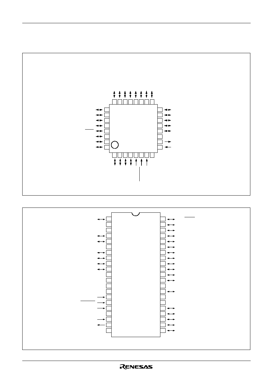
Fig. 3 Pin configuration (42S1M type)
Fig. 2 Pin configuration (32P6U-A type)
Package type : 32P6U-A
32
31
30
29
28
27
26
25
9
10
11
12
13
14
15
16
8
7
6
5
3
4
V
CC
CNV
SS
P2
2
/AN
2
P0
5
(LED
5
)
P0
2
(LED
2
)
P0
4
(LED
4
)
P0
3
(LE
D3
)/TX
OUT
P0
6
(LED
6
)
P0
1
(LED
1
)
P0
0
(LED
0
)/CNTR
1
P3
7
(LED
13
)/INT
0
M37544M2-XXXGP
M37544G2GP
P2
3
/AN
3
P2
4
/AN
4
P2
5
/AN
5
V
REF
RESET
1
2
P2
0
/
AN
0
P2
1
/
AN
1
P1
4
/CNTR
0
P1
3
/S
RDY
P1
2
/S
CLK
P1
1
/T
X
D
P1
0
/R
X
D
P0
7
(LED
7
)
X
OUT
X
IN
V
SS
P3
0
(LED
8
)
P3
1
(LED
9
)
P3
2
(LED
10
)
P3
3
(LED
11
)
P3
4
(LED
12
)/INT
1
24
23
22
21
20
19
18
17
Outline 42S1M
P0
0
(LED
0
)/CNTR
1
CNV
SS
X
OUT
X
IN
V
SS
P0
1
(LED
1
)
P0
2
(LED
2
)
P0
3
(LED
3
)/TX
OUT
P0
4
(LED
4
)
P3
0
(LED
8
)
Vcc
V
REF
P0
5
(LED
5
)
P1
2
/S
CLK
P2
5
/AN
5
P1
4
/CNTR
0
NC
P2
2
/AN
2
NC
P2
1
/AN
1
P2
0
/AN
0
P3
1
(LED
9
)
NC
P2
3
/AN
3
P2
4
/AN
4
P0
6
(LED
6
)
P0
7
(LED
7
)
P3
7
(LED
13
)/INT
0
RESET
NC
NC
P3
4
(LED
12
)/INT
1
P3
3
(LED
11
)
P3
2
(LED
10
)
NC
P1
0
/R
X
D
P1
1
/T
X
D
NC
NC
P1
3
/S
RDY
1
2
3
4
5
6
7
8
9
10
11
12
13
14
15
16
17
18
19
20
21
42
41
40
39
38
37
36
35
34
33
32
31
30
29
28
27
26
25
24
23
22
M37544RSS
NC
NC

Rev.1.01 2003.05.06 page 3 of 53
7544 Group
PRELIMINARY
Notice: This is not a final specification.
Some parametric limits are subject to change.
FUNCTIONAL BLOCK
Fig. 4 Functional block diagram (32P4B package)
FUNCTIONAL BLOCK DIAGRAM (Package: 32P4B)
16
11
13
12
P1(5)
31
31
2
32
5
4
P2(6)
P3(6)
17
20
18
10
14
15
9
7
8
6
0
19
21
22
P0(8)
30
28
26
24
29
27
25
23
A-D
converter
(8)
X
IN
OUT
X
CPU
V
SS
RESET
V
CC
CNV
SS
I/O port P2
I/O port P0
I/O port P1
I/O port P3
SI/O(8)
RAM
ROM
A
X
Y
S
PC
H
PC
L
PS
Reset input
Clock generating circuit
Clock input
Clock output
V
REF
Watchdog timer
Reset
INT
0
CNTR
0
Timer X (8)
Key-on wakeup
Prescaler X (8)
CNTR
1
Timer A (16)
Timer 1 (8)
Prescaler 1 (8)
TX
OUT
INT
1

Rev.1.01 2003.05.06 page 4 of 53
7544 Group
PRELIMINARY
Notice: This is not a final specification.
Some parametric limits are subject to change.
Fig. 5 Functional block diagram (32P6U package)
FUNCTIONAL BLOCK DIAGRAM (Package: 32P6U)
X
IN
OUT
X
SI/O(8)
RAM
ROM
CPU
A
X
Y
S
PC
H
PC
L
PS
V
SS
11
RESET
6
V
CC
8
7
CNV
SS
P1(5)
30
28
26
29
27
32
31
P2(6)
P3(6)
12
15
13
5
Reset input
I/O port P2
I/O port P1
I/O port P3
Clock generating circuit
Clock input
Clock output
9
10
4
2
3
1
A-D
converter
(8)
V
REF
Watchdog timer
Reset
0
14
INT
0
16
17
CNTR
0
I/O port P0
Timer X (8)
Key-on wakeup
Prescaler X (8)
CNTR
1
Timer A (16)
P0(8)
25
23
21
19
24
22
20
18
Timer 1 (8)
Prescaler 1 (8)
TX
OUT
INT
1
Rev.1.01 2003.05.06 page 5 of 53
7544 Group
PRELIMINARY
Notice: This is not a final specification.
Some parametric limits are subject to change.
PIN DESCRIPTION
Table 1 Pin description
Function
∑Apply voltage of 4.0 to 5.5 V to Vcc, and 0 V to Vss.
∑Reference voltage input pin for A-D converter
∑Chip operating mode control pin, which is always connected to Vss.
∑Reset input pin for active "L"
∑Input and output pins for main clock generating circuit
∑Connect a ceramic resonator or quartz-crystal oscillator between the X
IN
and X
OUT
pins.
∑For using RC oscillator, short between the X
IN
and X
OUT
pins, and connect the capacitor and resistor.
∑If an external clock is used, connect the clock source to the X
IN
pin and leave the X
OUT
pin open.
∑ When the ring oscillator is selected as the main clock, connect X
IN
pin to V
CC
and leave X
OUT
open.
Function expect a port function
Name
Power source
Analog reference
voltage
CNVss
Reset input
Clock input
I/O port P0
I/O port P1
Pin
Vcc, Vss
V
REF
CNVss
______
RESET
X
IN
P0
0
/CNTR
1
P0
1
P0
2
P0
3
/TX
OUT
P0
4
≠P0
7
∑ Key-input (key-on wake up
interrupt input) pins
∑ Timer X and timer A function
pin
∑8-bit I/O port.
∑I/O direction register allows each pin to be individually pro-
grammed as either input or output.
∑CMOS compatible input level
∑CMOS 3-state output structure
∑P0 can output a large current for driving LED.
∑Whether a built-in pull-up resistor is to be used or not can be de-
termined by program.
∑5-bit I/O port
∑I/O direction register allows each pin to be individually pro-
grammed as either input or output.
∑CMOS compatible input level
∑CMOS 3-state output structure
∑CMOS/TTL level can be switched for P1
0
and P1
2
∑6-bit I/O port having almost the same function as P0
∑CMOS compatible input level
∑CMOS 3-state output structure
P1
0
/RxD
P1
1
/TxD
P1
2
/S
CLK
____
P1
3
/S
RDY
P1
4
/CNTR
0
P2
0
/AN
0
≠P2
5
/AN
5
P3
0
≠P3
3
P3
4
/INT
1
P3
7
/INT
0
I/O port P2
I/O port P3
∑ Serial I/O function pin
∑ Timer X function pin
∑ Input pins for A-D converter
∑ Interrupt input pins
∑6-bit I/O port
∑I/O direction register allows each pin to be individually programmed as either input or output.
∑CMOS compatible input level (CMOS/TTL level can be switched for P3
4
and P3
7
).
∑CMOS 3-state output structure
∑P3 can output a large current for driving LED.
X
OUT
Clock output
∑Whether a built-in pull-up resistor is to be used or not can be de-
termined by program.