Document Outline
- ˛ˇ
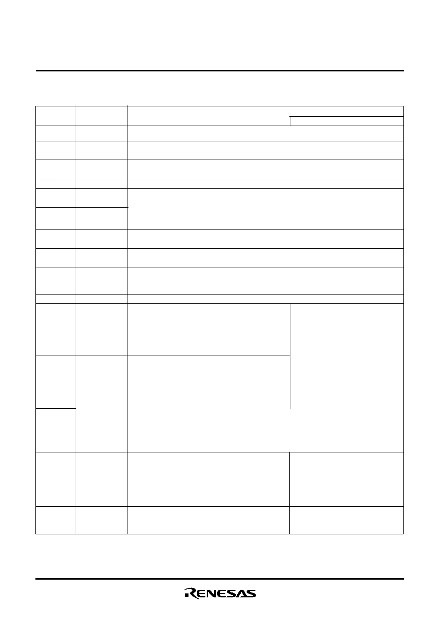
- ˛ˇ
- ˛ˇ
- ˛ˇ
- Package type: 100P6S-A
- Package type: 100P6Q-A
- FUNCTIONAL BLOCK DIAGRAM
- ˛ˇ
- ˛ˇ
- ˛ˇ
- ˛ˇ
- ˛ˇ
- ˛ˇ
- ˛ˇ
- ˛ˇ
- ˛ˇ
- ˛ˇ
- ˛ˇ
- ˛ˇ
- ˛ˇ
- ˛ˇ
- ˛ˇ
- Bias Control and Applied Voltage to LCD Power Input Pins
- ˛ˇ
- ˛ˇ
- ˛ˇ
- ˛ˇ
- ˛ˇ
- ˛ˇ
- ˛ˇ
- ˛ˇ
- ˛ˇ
- ˛ˇ
- ˛ˇ
- ˛ˇ
- Absolute maximum ratings
- Recommended operating conditions
- ˛ˇ
- ˛ˇ
- ˛ˇ
- ˛ˇ
- ˛ˇ
- Timing diagram
- ˛ˇ
- ˛ˇ

Regarding the change of names mentioned in the document, such as Mitsubishi
Electric and Mitsubishi XX, to Renesas Technology Corp.
The semiconductor operations of Hitachi and Mitsubishi Electric were transferred to Renesas
Technology Corporation on April 1st 2003. These operations include microcomputer, logic, analog
and discrete devices, and memory chips other than DRAMs (flash memory, SRAMs etc.)
Accordingly, although Mitsubishi Electric, Mitsubishi Electric Corporation, Mitsubishi
Semiconductors, and other Mitsubishi brand names are mentioned in the document, these names
have in fact all been changed to Renesas Technology Corp. Thank you for your understanding.
Except for our corporate trademark, logo and corporate statement, no changes whatsoever have been
made to the contents of the document, and these changes do not constitute any alteration to the
contents of the document itself.
Note : Mitsubishi Electric will continue the business operations of high frequency & optical devices
and power devices.
Renesas Technology Corp.
Customer Support Dept.
April 1, 2003
To all our customers

DESCRIPTION
The 7560 group (A version) is the 8-bit microcomputer based on
the 740 family core technology.
The 7560 group (A version) has the LCD drive control circuit, an 8-
channel A-D converter, D-A converter, serial I/O and PWM as ad-
ditional functions.
The various microcomputers in the 7560 group (A version) include
variations of internal memory size and packaging. For details, re-
fer to the section on part numbering.
For details on availability of microcomputers in the 7560 group (A
version), refer the section on group expansion.
FEATURES
∑
Basic machine-language instructions ....................................... 71
∑
The minimum instruction execution time ............................ 0.4
µ
s
(at 10 MHz oscillation frequency)
∑
Memory size
ROM ................................................................ 32 K to 60 K bytes
RAM ............................................................... 1024 to 2560 bytes
∑
Programmable input/output ports ............................................. 55
∑
Software pull-up resistors .................................................... Built-in
∑
Output ports ................................................................................. 8
∑
Input ports .................................................................................... 1
∑
Interrupts .................................................. 17 sources, 16 vectors
External ................ 7 sources (includes key input interrupt)
Internal ................................................................ 9 sources
Software ................................................................ 1 source
∑
Timers ............................................................ 8-bit
3, 16-bit
2
∑
Serial I/O1 ..................... 8-bit
1 (UART or Clock-synchronous)
∑
Serial I/O2 .................................... 8-bit
1 (Clock-synchronous)
∑
PWM output .................................................................... 8-bit
1
∑
A-D converter ................................................ 10-bit
8 channels
∑
D-A converter .................................................. 8-bit
2 channels
∑
LCD drive control circuit
Bias ......................................................................... 1/2, 1/3
Duty .................................................................. 1/2, 1/3, 1/4
Common output ................................................................ 4
Segment output .............................................................. 40
∑
2 Clock generating circuits
(connect to external ceramic resonator or quartz-crystal oscillator)
∑
Watchdog timer ............................................................. 14-bit
1
∑
Power source voltage
In high-speed mode (f(X
IN
) = 10 MHz) ................... 4.5 V to 5.5 V
In high-speed mode (f(X
IN
) = 8 MHz) ..................... 4.0 V to 5.5 V
In middle-speed mode (f(X
IN
) = 6 MHz) ................. 1.8 V to 5.5 V
In low-speed mode .................................................. 1.8 V to 5.5 V
∑
Power dissipation
In high-speed mode ........................................................... 23 mW
(at 10MHz oscillation frequency, at 5 V power source voltage)
In low-speed mode .............................................................. 27
µ
W
(at 32 kHz oscillation frequency, at 3 V power source voltage)
∑
Operating temperature range ................................... ≠ 20 to 85∞C
APPLICATIONS
Camera, household appliances, consumer electronics, etc.
7560 Group (A Version)
MITSUBISHI MICROCOMPUTERS
SINGLE-CHIP 8-BIT CMOS MICROCOMPUTER
PRELIMINAR
Y
Notice: This is not a final specification.
Some parametric limits are subject to change.

SINGLE-CHIP 8-BIT CMOS MICROCOMPUTER
MITSUBISHI MICROCOMPUTERS
7560 Group (A Version)
2
PRELIMINAR
Y
Notice: This is not a final specification.
Some parametric limits are subject to change.
Package type : 100P6Q-A
PIN CONFIGURATION (TOP VIEW)
Fig. 2 Pin configuration (Package type: 100P6Q-A)
1
2 3
4 5
6
7
8
9 1
0 11 1
2 13 1
4 15 1
6 17 1
8 19 2
0 21 22 2
3 2
4 25
26
27
28
29
30
31
32
33
34
35
36
37
38
39
40
41
42
43
44
45
46
47
48
49
50
5
1
5
2
5
3
54
55
5
6
57
5
8
59
6
0
61
6
2
63
6
4
65
6
6
67
6
8
69
7
0
71
7
2
7
3
7
4
7
5
7
6
7
7
7
8
79
8
0
8
1
8
2
8
3
8
4
8
5
8
6
8
7
8
8
8
9
9
0
9
1
9
2
9
3
9
4
9
5
96
9
7
9
8
9
9
0
0
1
M
3
7
5
6
0
M
X
A
-
X
X
X
G
P
S
E
G
1
2
SEG
11
S
E
G
1
0
S
E
G
9
SEG
8
S
E
G
7
S
E
G
6
S
E
G
5
S
E
G
4
S
E
G
3
S
E
G
2
S
E
G
1
S
E
G
0
V
C
C
V
REF
AV
SS
C
O
M
3
C
O
M
2
COM
1
C
O
M
0
V
L
3
V
L
2
C
2
C
1
V
L
1
P
6
7
/
A
N
7
P
6
6
/
A
N
6
P
6
5
/
A
N
5
P
6
4
/
A
N
4
P
5
7
/
A
D
T
/
D
A
2
P
5
6
/
D
A
1
P
5
5
/
C
N
T
R
1
P
5
4
/
C
N
T
R
0
P
4
1
/
I
N
T
1
P
4
0
P
4
3
/
/
T
O
U
T
P
5
3
/
R
T
P
1
P
5
2
/
R
T
P
0
P
5
1
/
P
W
M
1
P
5
0
/
P
W
M
0
P
7
7
P
4
2
/
I
N
T
2
P7
2
P7
3
P7
1
P7
0
/INT
0
X
CIN
X
COUT
X
IN
X
OUT
V
SS
P2
7
P2
6
P2
5
P2
4
P2
3
P2
1
P1
6
P2
2
P2
0
P1
7
RESET
P7
6
P7
5
P7
4
P1
5
/SEG
39
P1
4
/SEG
38
P
3
1
/
S
E
G
1
9
P
3
0
/
S
E
G
1
8
P
3
2
/
S
E
G
2
0
P
3
3
/
S
E
G
2
1
P
3
4
/
S
E
G
2
2
S
E
G
1
3
S
E
G
1
4
S
E
G
1
5
P
3
5
/
S
E
G
2
3
P
3
6
/
S
E
G
2
4
P
3
7
/
S
E
G
2
5
P
0
0
/
S
E
G
2
6
P
0
1
/
S
E
G
2
7
P
0
2
/
S
E
G
2
8
P
0
3
/
S
E
G
2
9
P
0
4
/
S
E
G
3
0
P
0
5
/
S
E
G
3
1
P
0
6
/
S
E
G
3
2
P
0
7
/
S
E
G
3
3
P
1
0
/
S
E
G
3
4
P
1
1
/
S
E
G
3
5
P
1
2
/
S
E
G
3
6
P
1
3
/
S
E
G
3
7
S
E
G
1
6
S
E
G
1
7
P
6
2
/
S
C
L
K
2
1
/
A
N
2
P
6
1
/
S
O
U
T
2
/
A
N
1
P
6
0
/
S
I
N
2
/
A
N
0
P
6
3
/
S
C
L
K
2
2
/
A
N
3
P
4
6
/
S
C
L
K
1
P
4
5
/
T
X
D
P
4
4
/
R
X
D
P
4
7
/
S
R
D
Y
1
Package type : 100P6S-A
Fig. 1 Pin configuration (Package type: 100P6S-A)
PIN CONFIGURATION (TOP VIEW)
1
2 3
4 5
6
7
8
9 10 11 1
2 1
3 14 15 16 17 18 19 2
0 21 2
2 2
3 2
4 2
5 2
6 27 28 29 30
31
32
33
34
35
36
37
38
39
40
41
42
43
44
45
46
47
48
49
50
5
1
5
2
5
3
5
4
5
5
5
6
5
7
58
5
9
6
0
61
6
2
6
3
6
4
6
5
6
6
6
7
6
8
6
9
70
7
1
72
73
7
4
7
5
7
6
7
7
7
8
7
9
8
0
8
1
8
2
8
3
84
8
5
8
6
8
7
8
8
8
9
9
0
9
1
9
2
9
3
9
4
9
5
96
9
7
9
8
99
10
0
M
3
7
5
6
0
M
X
A
-
X
X
X
F
P
S
E
G
9
P
3
1
/
S
E
G
1
9
P
3
0
/
S
E
G
1
8
P
3
2
/
S
E
G
2
0
P
3
3
/
S
E
G
2
1
P
3
4
/
S
E
G
2
2
S
E
G
1
0
S
E
G
1
1
S
E
G
1
2
S
E
G
1
3
S
E
G
1
4
S
E
G
1
5
P
3
5
/
S
E
G
2
3
P
3
6
/
S
E
G
2
4
P
3
7
/
S
E
G
2
5
P
0
0
/
S
E
G
2
6
P
0
1
/
S
E
G
2
7
P
0
2
/
S
E
G
2
8
P
0
3
/
S
E
G
2
9
P
0
4
/
S
E
G
3
0
P
0
5
/
S
E
G
3
1
P
0
6
/
S
E
G
3
2
P
0
7
/
S
E
G
3
3
P
1
0
/
S
E
G
3
4
P
1
1
/
S
E
G
3
5
P
1
2
/
S
E
G
3
6
P
1
3
/
S
E
G
3
7
P
1
4
/
S
E
G
3
8
P
1
5
/
S
E
G
3
9
C
1
V
L
1
P
6
7
/
A
N
7
P
6
6
/
A
N
6
P
6
5
/
A
N
5
P
6
4
/
A
N
4
P
6
2
/
S
C
L
K
2
1
/
A
N
2
P
6
1
/
S
O
U
T
2
/
A
N
1
P
6
0
/
S
I
N
2
/
A
N
0
P
5
7
/
A
D
T
/
D
A
2
P
5
6
/
D
A
1
P
5
5
/
C
N
T
R
1
P
5
4
/
C
N
T
R
0
P
5
3
/
R
T
P
1
P
5
2
/
R
T
P
0
P
5
1
/
P
W
M
1
P
5
0
/
P
W
M
0
P
4
6
/
S
C
L
K
1
P
4
5
/
T
X
D
P
4
4
/
R
X
D
P
4
3
/
/
T
O
U
T
P
4
2
/
I
N
T
2
P
4
1
/
I
N
T
1
P
4
0
P
7
7
P
7
6
P
7
5
P
7
4
C
2
V
L2
V
L3
COM
0
C
O
M
1
COM
2
V
R
E
F
A
V
S
S
V
C
C
S
E
G
8
S
E
G
0
S
E
G
1
S
E
G
2
S
E
G
4
S
E
G
5
S
E
G
6
S
E
G
7
S
E
G
3
P7
2
P7
3
P7
1
P7
0
/INT
0
X
CIN
X
COUT
X
IN
X
OUT
V
SS
P2
7
P2
6
P2
5
P2
4
P2
3
P2
1
P1
6
P2
2
P2
0
P1
7
RESET
S
E
G
1
6
S
E
G
1
7
C
O
M
3
P
4
7
/
S
R
D
Y
1
P
6
3
/
S
C
L
K
2
2
/
A
N
3

SINGLE-CHIP 8-BIT CMOS MICROCOMPUTER
MITSUBISHI MICROCOMPUTERS
7560 Group (A Version)
3
PRELIMINAR
Y
Notice: This is not a final specification.
Some parametric limits are subject to change.
FUNCTIONAL BLOCK DIAGRAM (Package type: 100P6S-A)
Fig. 3 Functional block diagram
I
N
T
1
,
I
N
T
2
C
N
T
R
0
,
C
N
T
R
1
D
A
1
A
D
T
C
P
U
A
X
Y
S
P
C
H
P
C
L
P
S
R
E
S
E
T
V
C
C
V
S
S
(
5
V
)
(
0
V
)
R
O
M
R
A
M
3
5
9
1
4
0
P
4
(
8
)
P
2
(
8
)
P
0
(
8
)
P
1
(
8
)
P
6
(
8
)
P
7
(
8
)
P
3
(
8
)
P
5
(
8
)
1
2
1
0
0
9
9
9
8
9
7
9
6
9
5
9
4
9
0
8
9
8
8
8
7
8
6
8
5
8
4
8
3
8
2
8
1
8
0
7
9
7
8
7
7
7
6
7
5
7
4
7
3
5
7
5
8
5
9
6
0
6
1
6
2
6
3
6
4
4
9
5
0
5
1
5
2
5
3
5
4
5
5
5
6
4
1
4
2
4
3
4
4
4
5
4
6
4
7
4
8
6
5
6
6
6
7
6
8
6
9
7
0
7
1
7
2
1
9
2
0
2
1
2
2
2
3
2
4
2
5
2
6
3
6
3
7
2
7
2
8
2
9
3
0
3
1
3
2
3
3
3
4
3
4
5
6
7
8
9
1
0
9
3
9
2
1
1
1
2
1
3
1
4
1
5
1
6
1
7
1
8
X
C
I
N
X
C
O
U
T
X
I
N
O
U
T
X
C
O
U
T
X
X
C
I
N
S
I
/
O
1
(
8
)
V
R
E
F
A
V
S
S
V
L
1
C
1
C
2
V
L
2
V
L
3
C
O
M
0
C
O
M
1
C
O
M
2
C
O
M
3
S
E
G
0
S
E
G
1
S
E
G
2
S
E
G
3
S
E
G
4
S
E
G
5
S
E
G
6
S
E
G
7
S
E
G
8
S
E
G
9
S
E
G
1
0
S
E
G
1
1
S
E
G
1
2
S
E
G
1
3
S
E
G
1
4
S
E
G
1
5
S
E
G
1
6
S
E
G
1
7
X
C
I
N
C
O
U
T
X
3
8
3
9
S
I
/
O
2
(
8
)
P
W
M
(
8
)
I
N
T
0
D
-
A
2
D
-
A
1
D
A
2
T
O
U
T
L
C
D
d
r
i
v
e
c
o
n
t
r
o
l
c
i
r
c
u
i
t
L
C
D
d
i
s
p
l
a
y
R
A
M
(
2
0
b
y
t
e
s
)
T
i
m
e
r
X
(
1
6
)
T
i
m
e
r
Y
(
1
6
)
T
i
m
e
r
1
(
8
)
T
i
m
e
r
2
(
8
)
T
i
m
e
r
3
(
8
)
D
a
t
a
b
u
s
C
l
o
c
k
g
e
n
e
r
a
t
i
n
g
c
i
r
c
u
i
t
M
a
i
n
c
l
o
c
k
i
n
p
u
t
M
a
i
n
cl
o
c
k
o
u
t
p
u
t
S
u
b
-
c
l
o
c
k
o
u
t
p
u
t
S
u
b
-
c
l
o
c
k
i
n
p
u
t
R
e
s
e
t
K
e
y
i
n
p
u
t
(
K
e
y
-
o
n
w
a
k
e
u
p
)
i
n
t
e
r
r
u
p
t
R
e
a
l
t
i
m
e
p
o
r
t
f
u
n
c
t
i
o
n
A
-
D
c
o
n
v
e
r
t
e
r
(
8
)
I
/
O
p
o
r
t
P
0
I
/
O
p
o
r
t
P
1
I
/
O
p
o
r
t
P
2
I
/
O
p
o
r
t
P
4
I
/
O
p
o
r
t
P
5
I
/
O
p
o
r
t
P
6
O
u
t
p
u
t
p
o
r
t
P
3
I
/
O
p
o
r
t
P
7
R
e
s
e
t
i
n
p
u
t
S
u
b
-
c
l
o
c
k
o
u
t
p
u
t
S
u
b
-
c
l
o
c
k
i
n
p
u
t
W
a
t
c
h
d
o
g
t
i
m
e
r
SINGLE-CHIP 8-BIT CMOS MICROCOMPUTER
MITSUBISHI MICROCOMPUTERS
7560 Group (A Version)
4
PRELIMINAR
Y
Notice: This is not a final specification.
Some parametric limits are subject to change.
PIN DESCRIPTION
Table 1 Pin description (1)
V
CC
V
SS
Function
Pin
Name
Function except a port function
∑LCD segment output pins
Power source
∑Apply voltage of 1.8 V to V
CC
, and 0 V to V
SS
.
V
REF
AV
SS
RESET
X
IN
X
OUT
V
L1
≠V
L3
C
1
, C
2
COM
0
≠COM
3
SEG
0
≠SEG
17
P0
0
/SEG
26
≠
P0
7
/SEG
33
P1
0
/SEG
34
≠
P1
5
/SEG
39
P1
6
, P1
7
P2
0
≠ P2
7
P3
0
/SEG
18
≠
P3
7
/SEG
25
Analog refer-
ence voltage
Analog power
source
Reset input
Clock input
Clock output
LCD power
source
Charge-pump
capacitor pin
Common output
Segment output
I/O port P0
I/O port P1
I/O port P2
Output port P3
∑Reference voltage input pin for A-D converter and D-A converter.
∑GND input pin for A-D converter and D-A converter.
∑Connect to V
SS
.
∑Reset input pin for active "L".
∑Input and output pins for the main clock generating circuit.
∑Connect a ceramic resonator or a quartz-crystal oscillator between the X
IN
and X
OUT
pins to set
the oscillation frequency.
∑If an external clock is used, connect the clock source to the X
IN
pin and leave the X
OUT
pin open. A
feedback resistor is built-in.
∑Input 0
V
L1
V
L2
V
L3
voltage.
∑Input 0 ≠ V
L3
voltage to LCD. (0
V
L1
V
L2
V
L3
when a voltage is multiplied.)
∑External capacitor pins for a voltage multiplier (3 times) of LCD control.
∑LCD common output pins.
∑COM
2
and COM
3
are not used at 1/2 duty ratio.
∑COM
3
is not used at 1/3 duty ratio.
∑LCD segment output pins.
∑8-bit I/O port.
∑CMOS compatible input level.
∑CMOS 3-state output structure.
∑Pull-up control is enabled.
∑I/O direction register allows each 8-bit pin to be pro-
grammed as either input or output.
∑6-bit I/O port.
∑CMOS compatible input level.
∑CMOS 3-state output structure.
∑Pull-up control is enabled.
∑I/O direction register allows each 6-bit pin to be pro-
grammed as either input or output.
∑2-bit I/O port.
∑CMOS compatible input level.
∑CMOS 3-state output structure.
∑I/O direction register allows each pin to be individually programmed as either input or output.
∑Pull-up control is enabled.
∑8-bit I/O port.
∑CMOS compatible input level.
∑CMOS 3-state output structure.
∑I/O direction register allows each pin to be individually
programmed as either input or output.
∑Pull-up control is enabled.
∑8-bit output.
∑CMOS 3-state output structure.
∑Port output control is enabled.
∑Key input (key-on wake-up) interrupt
input pins
∑LCD segment output pins