 | –≠–Ľ–Ķ–ļ—ā—Ä–ĺ–Ĺ–Ĺ—č–Ļ –ļ–ĺ–ľ–Ņ–ĺ–Ĺ–Ķ–Ĺ—ā: M37905M8C | –°–ļ–į—á–į—ā—Ć:  PDF PDF  ZIP ZIP |
Document Outline
- Ģˇ
- Ģˇ
- Ģˇ
- Ģˇ
- Ģˇ
- Ģˇ
- Ģˇ
- Ģˇ
- Ģˇ
- Ģˇ
- Ģˇ
- Ģˇ
- CLOCK SYNCHRONOUS SERIAL COMMUNICATION
- Ģˇ
- Ģˇ
- Ģˇ
- Ģˇ
- Ģˇ
- Ģˇ
- Ģˇ
- Ģˇ
- Ģˇ
- Ģˇ
- Ģˇ
- Ģˇ
- Ģˇ
- Ģˇ
- Ģˇ
- Ģˇ
- Ģˇ
- Ģˇ
- Ģˇ
- EXTERNAL CLOCK INPUT
- Ģˇ
- Ģˇ
- Ģˇ
- Corrections and Supplementary Explanation (REV.B)

Regarding the change of names mentioned in the document, such as Mitsubishi
Electric and Mitsubishi XX, to Renesas Technology Corp.
The semiconductor operations of Hitachi and Mitsubishi Electric were transferred to Renesas
Technology Corporation on April 1st 2003. These operations include microcomputer, logic, analog
and discrete devices, and memory chips other than DRAMs (flash memory, SRAMs etc.)
Accordingly, although Mitsubishi Electric, Mitsubishi Electric Corporation, Mitsubishi
Semiconductors, and other Mitsubishi brand names are mentioned in the document, these names
have in fact all been changed to Renesas Technology Corp. Thank you for your understanding.
Except for our corporate trademark, logo and corporate statement, no changes whatsoever have been
made to the contents of the document, and these changes do not constitute any alteration to the
contents of the document itself.
Note : Mitsubishi Electric will continue the business operations of high frequency & optical devices
and power devices.
Renesas Technology Corp.
Customer Support Dept.
April 1, 2003
To all our customers

M37905M4C-XXXFP, M37905M4C-XXXSP
M37905M6C-XXXFP, M37905M6C-XXXSP
M37905M8C-XXXFP, M37905M8C-XXXSP
PRELIMINAR
Y
Notice: This is not a final specification.
Some parametric limits are subject to change.
16-BIT CMOS MICROCOMPUTER
MITSUBISHI MICROCOMPUTERS
DESCRIPTION
These are single-chip 16-bit microcomputers designed with high-per-
formance CMOS silicon gate technology, being packaged in 64-pin
plastic molded QFP or shrink plastic molded SDIP. These microcom-
puters support the 7900 Series instruction set, which are enhanced
and expanded instruction set and are upper-compatible with the
7700/7751 Series instruction set.
The CPU of these microcomputers is a 16-bit parallel processor that
can also be switched to perform 8-bit parallel processing. Also, the
bus interface unit of these microcomputers enhances the memory
access efficiency to execute instructions fast. Therefore, these mi-
crocomputers are suitable for office, business, and industrial equip-
ment controller that require high-speed processing of large data.
Also, they are suitable for motor-control equipment since each of
them includes the motor control circuit.
DISTINCTIVE FEATURES
∑
Number of basic machine instructions .................................... 203
∑
Memory
[M37905M4C-XXXFP, M37905M4C-XXXSP]
ROM .............................................................................. 32 Kbytes
RAM ............................................................................. 1024 bytes
[M37905M6C-XXXFP, M37905M6C-XXXSP]
ROM .............................................................................. 48 Kbytes
RAM ............................................................................. 3072 bytes
[M37905M8C-XXXFP, M37905M8C-XXXSP]
ROM .............................................................................. 60 Kbytes
RAM ............................................................................. 3072 bytes
∑
Instruction execution time
The fastest instruction at 20 MHz frequency ........................ 50 ns
∑
Single power supply .................................................... 5 V Ī 0.5 V
∑
Interrupts ........... 8 external sources, 23 internal sources, 7 levels
∑
Multi-functional 16-bit timer ................................................. 10 + 3
(Three-phase motor drive waveform and Pulse motor drive wave-
form output are available.)
∑
Serial I/O (UART or Clock synchronous) ..................................... 3
∑
10-bit A-D converter .......................................... 12-channel inputs
∑
8-bit D-A converter ............................................ 2-channel outputs
∑
12-bit watchdog timer
∑
Programmable input/output (ports P1, P2, P4, P5, P6, P7, P8) .. 50
APPLICATION
Control devices for office equipment such as copiers and facsimiles
Control devices for industrial equipment such as communication
and measuring instruments
Control devices for equipment, requiring motor control, such as
inverter air conditioners and general-purpose inverters
1
2
3
4
5
6
7
8
9
10
11
12
13
14
15
16
22
21
20
19
18
17
P7
3
/AN
3
P7
2
/AN
2
P7
1
/AN
1
P6
5
/TA2
IN
/U/RTP1
1
P6
4
/TA2
OUT
/V/RTP1
0
P6
3
/TA1
IN
/W/RTP0
3
P6
2
/TA1
OUT
/U/RTP0
2
P6
1
/TA0
IN
/V/RTP0
1
P6
0
/TA0
OUT
/W/RTP0
0
P5
7
/INT
7
/TB2
IN
/IDU
P5
6
/INT
6
/TB1
IN
/IDV
P5
5
/INT
5
/TB0
IN
/IDW
P6OUT
CUT
/INT
4
48
47
46
45
44
43
42
41
40
39
38
37
36
35
49
50
51
52
53
54
55
56
57
58
59
60
61
62
63
64
34
33
32
31
30
29
28
27
26
25
24
23
P7
0
/AN
0
P6
7
/TA3
IN
/RTP1
3
P6
6
/TA3
OUT
/RTP1
2
MD0
RESET
X
IN
X
OUT
V
CONT
V
SS
P5
3
/INT
3
/RTP
TRG0
P5
2
/INT
2
/RTP
TRG1
P5
1
/INT
1
P4OUT
CUT
/INT
0
P4
7
/TA8
IN
/RTP3
3
P4
6
/TA8
OUT
/RTP3
2
P4
5
/TA7
IN
/RTP3
1
P4
4
/TA7
OUT
/RTP3
0
P4
3
/TA6
IN
/RTP2
3
P4
2
/TA6
OUT
/RTP2
2
P2
3
/TA9
IN
P2
2
/TA9
OUT
P2
1
/TA4
IN
P2
0
/TA4
OUT
P1
7
/TxD
1
P1
6
/RxD
1
P1
5
/CTS
1
/CLK
1
P1
4
/CTS
1
/RTS
1
P1
3
/TxD
0
P8
3
/AN
11
/T
X
D
2
P8
2
/AN
10
/R
X
D
2
P8
1
/AN
9
/CTS
2
/CLK
2
V
CC
AV
CC
V
REF
AV
SS
V
SS
P7
7
/AN
7
/DA
0
P7
6
/AN
6
P7
5
/AN
5
P7
4
/AN
4
P8
0
/AN
8
/CTS
2
/RTS
2
/DA
1
M37905M
X
C-XXXFP
P1
1
/CTS
0
/CLK
0
P1
0
/CTS
0
/RTS
0
P4
1
/TA5
IN
/RTP2
1
P4
0
/TA5
OUT
/RTP2
0
MD1
P2
7
P2
6
(/TB2
IN
)
P2
5
(/TB1
IN
)
P2
4
(/TB0
IN
)
P1
2
/R
X
D
0
Note
Note
M37905MxC-XXXFP PIN CONFIGURATION (TOP VIEW)
Outline 64P6N-A
Note : Allocation of pins TB0
IN
to TB2
IN
can be switched by software.
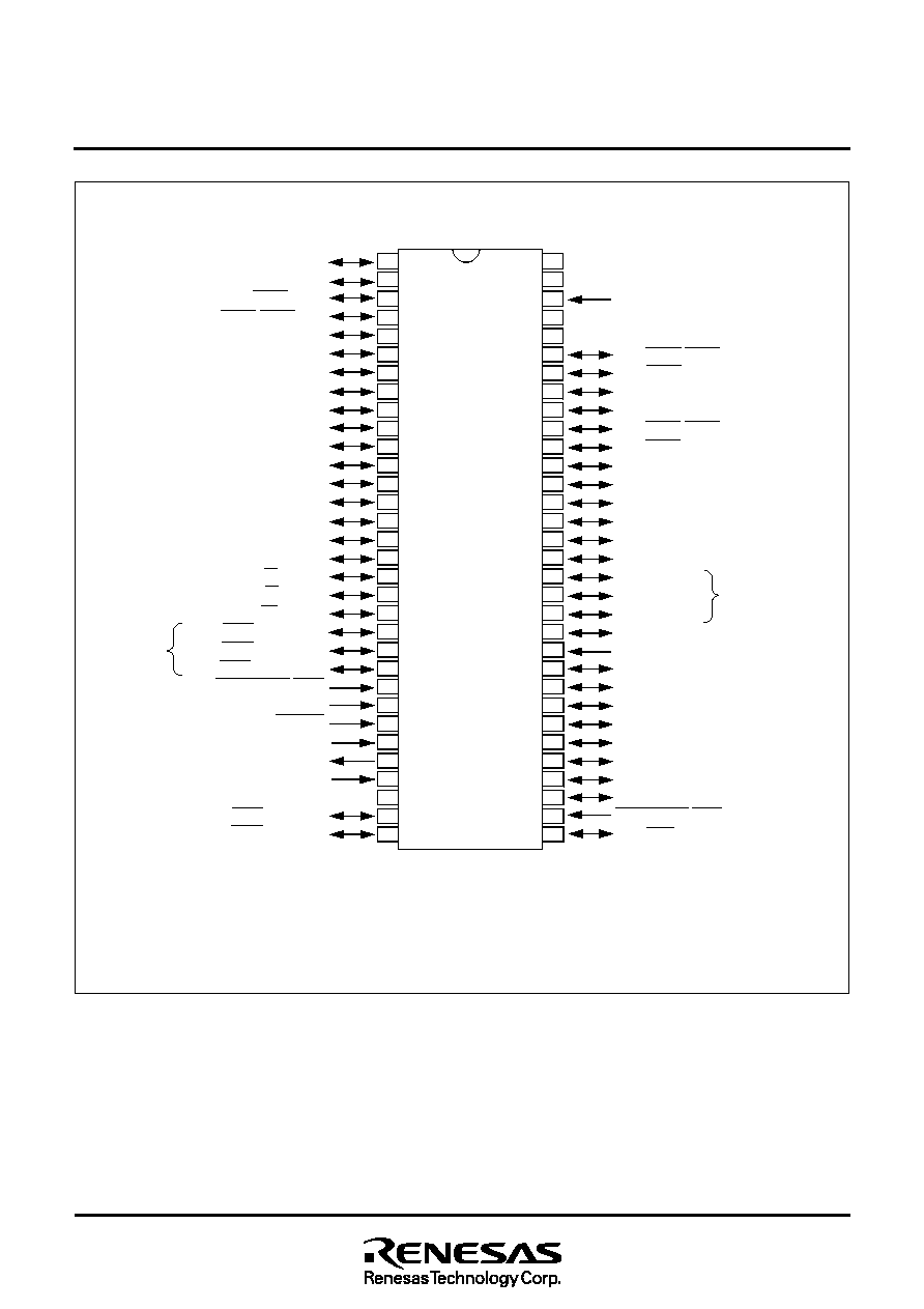
M37905M4C-XXXFP, M37905M4C-XXXSP
M37905M6C-XXXFP, M37905M6C-XXXSP
M37905M8C-XXXFP, M37905M8C-XXXSP
PRELIMINAR
Y
Notice: This is not a final specification.
Some parametric limits are subject to change.
16-BIT CMOS MICROCOMPUTER
MITSUBISHI MICROCOMPUTERS
2
M37905MxC-XXXSP PIN CONFIGURATION (TOP VIEW)
Outline 64P4B
63
64
2
1
P7
5
/AN
5
P7
6
/AN
6
P7
7
/AN
7
/
DA
0
P8
0
/AN
8
/
CTS
2
/RTS
2
/
DA
1
P8
2
/AN
10
/RxD
2
P8
1
/AN
9
/CTS
2
/CLK
2
P1
0
/CTS
0
/RTS
0
P1
1
/CTS
0
/CLK
0
P1
4
/CTS
1
/RTS
1
P2
0
/TA4
OUT
P2
1
/TA4
IN
P2
2
/TA9
OUT
P2
3
/TA9
IN
P2
5
(/TB1
IN
)
P2
6
(/TB2
IN
)
P2
7
MD1
V
SS
P2
4
(/TB0
IN
)
P1
5
/CTS
1
/CLK
1
P1
6
/RxD
1
AV
CC
P1
2
/RxD
0
P1
3
/TxD
0
P1
7
/TxD
1
62
44
45
46
47
48
49
50
51
52
53
54
56
57
58
59
60
61
55
3
21
20
19
18
17
16
15
14
13
12
11
9
8
7
6
5
4
10
V
REF
P6
5
/TA2
IN
/U/RTP1
1
P6
4
/TA2
OUT
/V/RTP1
0
P6
3
/TA1
IN
/W/RTP0
3
M37905M
X
C-XXXSP
32
31
30
29
28
27
26
25
24
23
22
P6
2
/TA1
OUT
/U/RTP0
2
P6
1
/TA0
IN
/V/RTP0
1
P6
0
/TA0
OUT
/W/RTP0
0
P5
7
/INT
7
/TB2
IN
/IDU
P5
6
/INT
6
/TB1
IN
/IDV
P5
5
/INT
5
/TB0
IN
/IDW
MD0
V
CONT
RESET
P6OUT
CUT
/INT
4
V
SS
P4
0
/TA5
OUT
/RTP2
0
P4
1
/TA5
IN
/RTP2
1
P4
2
/TA6
OUT
/RTP2
2
P4
4
/TA7
OUT
/RTP3
0
P4
5
/TA7
IN
/RTP3
1
P4
6
/TA8
OUT
/RTP3
2
P4
3
/TA6
IN
/RTP2
3
33
34
35
36
37
38
39
40
41
42
43
P8
3
/AN
11
/TxD
2
P7
3
/AN
3
P7
4
/AN
4
P7
1
/AN
1
P7
2
/AN
2
P7
0
/AN
0
P6
7
/TA3
IN
/RTP1
3
P6
6
/TA3
OUT
/RTP1
2
X
IN
X
OUT
P5
3
/INT
3
/RTP
TRG0
P5
2
/INT
2
/RTP
TRG1
V
CC
AV
SS
P4
7
/TA8
IN
/RTP3
3
P4OUT
CUT
/INT
0
P5
1
/INT
1
Note
Note
Note : Allocation of pins TB0
IN
to TB2
IN
can be switched by software.
Outline 64P4B
3
M37905M4C-XXXFP, M37905M4C-XXXSP
M37905M6C-XXXFP, M37905M6C-XXXSP
M37905M8C-XXXFP, M37905M8C-XXXSP
PRELIMINAR
Y
Notice: This is not a final specification.
Some parametric limits are subject to change.
16-BIT CMOS MICROCOMPUTER
MITSUBISHI MICROCOMPUTERS
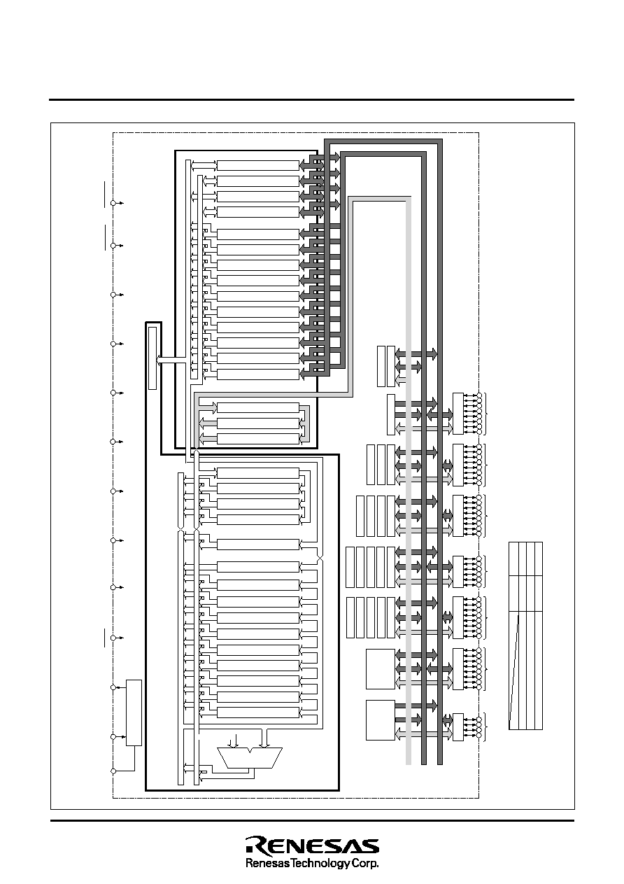
BLOCK DIAGRAM
Central Processing Unit (CPU)
Bus
Interface
Unit
(BIU)
RESET
MD1
V
Reference
Voltage Input
Instruction Register (8)
REF
(0V)
AV
SS
AV
CC
V
CC
X
Clock input
Clock Generating Circuit
Reset input
Clock output
IN
X
OUT
Address Bus
Data Bus (Odd)
Data Bus (Even)
A-D Converter (12)
UART1 (9)
UART0 (9)
Watchdog Timer
Timer TB1 (16)
Timer TB2 (16)
Timer TB0 (16)
D-A
1
Converter (8)
Timer TA1 (16)
Timer TA2 (16)
Timer TA3 (16)
Timer TA4 (16)
Timer TA0 (16)
RAM
(Note)
P6(8)
Input/Output P6
P5(6)
Input/Output P5
P7(8)
Input/Output P7
P4(8)
Input/Output P4
D-A
0
Converter (8)
P8(4)
Input/Output P8
MD0
(0V)
V
SS
P4OUT
CUT
ROM
(Note)
V
CONT
Timer TA6 (16)
Timer TA7 (16)
Timer TA8 (16)
Timer TA9 (16)
Timer TA5 (16)
P6OUT
CUT
P2(8)
Input/Output P2
P1(8)
Input/Output P1
UART2 (9)
M37905M4C-XXXFP, M37905M4C-XXXSP
M37905M6C-XXXFP, M37905M6C-XXXSP
M37905M8C-XXXFP, M37905M8C-XXXSP
ROM
32 Kbytes
48 Kbytes
60 Kbytes
RAM
1 Kbyte
3 Kbytes
3 Kbytes
Note:
Data Buffer DQ
0
(8)
Data Buffer DQ
1
(8)
Data Buffer DQ
2
(8)
Data Buffer DQ
3
(8)
Instruction Queue Buffer Q
0
(8)
Instruction Queue Buffer Q
1
(8)
Instruction Queue Buffer Q
2
(8)
Instruction Queue Buffer Q
3
(8)
Instruction Queue Buffer Q
4
(8)
Instruction Queue Buffer Q
5
(8)
Instruction Queue Buffer Q
6
(8)
Instruction Queue Buffer Q
7
(8)
Instruction Queue Buffer Q
8
(8)
Instruction Queue Buffer Q
9
(8)
Program Address Register PA (24)
Data Address Register DA (24)
Incrementer (24)
Incrementer/Decrementer (24)
Input Buffer Register IB (16)
Program Counter PC (16)
Program Bank Register PG (8)
Processor Status Register PS (11)
Direct Page Register DPR0 (16)
Direct Page Register DPR1 (16)
Direct Page Register DPR2 (16)
Direct Page Register DPR3 (16)
Stack Pointer S (16)
Index Register Y (16)
Index Register X (16)
Accumulator B (16)
Accumulator A (16)
Arithmetic Logic
Unit (16)
Data Bank Register DT (8)
M37905M4C-XXXFP, M37905M4C-XXXSP
M37905M6C-XXXFP, M37905M6C-XXXSP
M37905M8C-XXXFP, M37905M8C-XXXSP
PRELIMINAR
Y
Notice: This is not a final specification.
Som
e param
etric lim
its are subject to change.
16-BIT CMOS MICROCOMPUTER
MITSUBISHI MICROCOMPUTERS
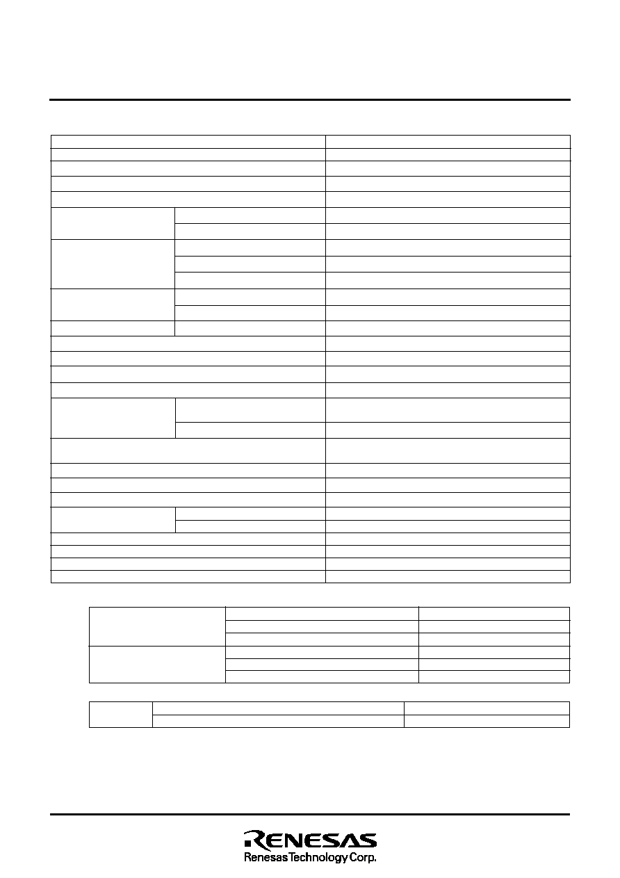
4
Memory expansion
Operating ambient temperature range
Device structure
Package
Ports' input/output
characteristics
Power supply voltage
Power dissipation
Number of basic machine instructions
Instruction execution time
External clock input frequency f(X
IN
)
System clock frequency f(f
sys
)
Memory size
Programmable input/output
ports
Multi-functional timers
Serial I/O
A-D converter
D-A converter
Dead-time timer
Watchdog timer
Interrupts
Clock generating circuit
PLL frequency multiplier
ROM
RAM
P1, P2, P4, P6, P7
P5
P8
TA0≠TA9
TB0≠TB2
UART0, UART1, and UART2
FUNCTIONS
Functions
Parameter
nput/Output withstand voltage
utput current
Maskable interrups
Non-maskable interrups
203
50 ns (the fastest instruction at f(f
sys
) = 20 MHz)
20 MHz (Max.)
20 MHz (Max.)
(Note 1)
(Note 1)
8-bit
5
6-bit
1
4-bit
1
16-bit
10
16-bit
3
(UART or Clock synchronous serial I/O)
3
10-bit successive approximation method
1 (12 channels)
8-bit
2
8-bit
3
12-bit
1
8 external sources, 20 internal sources. Each interrupt can be set
to a priority level within the range of 0≠7 by software.
3 internal sources
Incorporated (externally connected to a ceramic resonator or
quartz-crystal resonator).
The following multiplication ratios are available:
2,
3,
4.
5 VĪ0.5 V
125 mW (at f(f
sys
) = 20 MHz, Typ, ; the PLL frequency multiplier is inactive.)
5 V
5 mA
Not available (single-chip mode only).
≠20 to 85 įC
CMOS high-performance silicon gate process
(Note 2)
2:
Packages
M37905M4C-XXXFP, M37905M6C-XXXFP, M37905M8C-XXXFP
64-pin plastic molded QFP (64P6N-A)
M37905M4C-XXXSP, M37905M6C-XXXSP, M37905M8C-XXXSP
64-pin shrink plastic moldeds DIP (64P4B)
M37905M4C-XXXFP, M37905M4C-XXXSP
M37905M6C-XXXFP, M37905M6C-XXXSP
M37905M8C-XXXFP, M37905M8C-XXXSP
M37905M4C-XXXFP, M37905M4C-XXXSP
M37905M6C-XXXFP, M37905M6C-XXXSP
M37905M8C-XXXFP, M37905M8C-XXXSP
ROM
RAM
32 Kbytes
48 Kbytes
60 Kbytes
1024 bytes
3072 bytes
3072 bytes
Notes 1: