Document Outline
- ˛ˇ
- ˛ˇ
- ˛ˇ
- ˛ˇ
- ˛ˇ
- ˛ˇ
- ˛ˇ
- ˛ˇ
- ˛ˇ
- ˛ˇ
- ˛ˇ
- ˛ˇ
- ˛ˇ
- ˛ˇ
Rev.1.00
2004.04.13
page 1 of 16
REJ03C0101-0100Z
Rev.1.00
2004.04.13
R1LV1616R Series
16Mb superSRAM (1M wordx16bit)
Description
The R1LV1616R Series is a family of low voltage 16-Mbit static RAMs organized as 1048576-words by 16-bit,
fabricated by Renesas's high-performance 0.15um CMOS and TFT technologies.
The R1LV1616R Series is suitable for memory applications where a simple interfacing , battery operating and
battery backup are the important design objectives.
The R1LV1616R Series is packaged in a 52pin micro thin small outline mount device[µTSOP / 10.79mm x
10.49mm with the pin-pitch of 0.4mm] or a 48balls fine pitch ball grid array [f-BGA / 7.5mmx8.5mm with the ball-pitch
of 0.75mm and 6x8 array] . It gives the best solution for a compaction of mounting area as well as flexibility of wiring
pattern of printed circuit boards.
∑ Single 2.7-3.6V power supply
∑ Small stand-by current:2µA (3.0V, typ.)
∑ Data retention supply voltage =2.0V
∑ No clocks, No refresh
∑ All inputs and outputs are TTL compatible
∑ Easy memory expansion by CS1#, CS2, LB# and UB#
∑ Common Data I/O
∑ Three-state outputs: OR-tie capability
∑ OE# prevents data contention on the I/O bus
∑ Process technology: 0.15um CMOS
Features
R1LV1616R Series
Rev.1.00
2004.04.13
page 2 of 16
Ordering Information
85 ns
R1LV1616RBG-8S%
7.5mmx8.5mm f-BGA 0.75mm pitch 48ball
70 ns
R1LV1616RBG-7S%
85 ns
R1LV1616RSD-8S%
350-mil 52-pin plastic µ - TSOP(II)
(normal-bend type) (52PTG)
70 ns
R1LV1616RSD-7S%
Package
Access time
Type No.
% - Temperature version; see table below
-40 ~ +85 ∫C
I
-20 ~ +85 ∫C
W
0 ~ +70 ∫C
R
Temperature Range
%

R1LV1616R Series
Rev.1.00
2004.04.13
page 3 of 16
52-pin µTSOP
48-pin fBGA
1
2
3
4
5
6
A
B
C
D
E
F
G
DQ2
A7
DQ0
CS2
Vcc
Vss
DQ5
A2
CS1#
DQ1
DQ3
DQ4
DQ6
A1
A4
A6
A5
A17
A16
A15
A0
A3
A14
OE#
UB#
DQ14
DQ12
DQ11
DQ9
LB#
DQ15
DQ13
Vss
Vcc
DQ10
DQ7
WE#
A13
A12
A19
DQ8
N.C.
A11
A10
A9
A8
H
A18
NC
or
Vss
BYTE#
48
47
46
45
44
43
42
41
40
39
38
37
36
35
34
33
32
31
30
29
52
51
50
49
A16
DQ0
A0
Vss
OE#
DQ8
DQ1
DQ9
DQ2
NC
Vss
DQ10
DQ3
DQ11
DQ4
DQ12
DQ5
DQ13
DQ6
DQ14
DQ7
DQ15
1
2
3
4
5
6
7
8
9
10
11
12
13
14
15
16
A18
A17
A11
A10
A15
17
18
19
20
21
22
23
24
A13
A12
A14
A9
A8
A7
A6
A5
A4
A1
A2
A3
WE#
A19
Vcc
CS1#
28
27
25
26
LB#
CS2
NC
NC
NC
NC
UB#
NC
Pin Arrangement
Pin Description
Non connection
NC
Byte (x8 mode) enable input
BYTE#
Ground
Vss
Power supply
Vcc
Upper byte select
UB#
Lower byte select
LB#
Output enable
OE#
Write enable
WE#
Chip select
CS1# &CS2
Data input/output
DQ 0 to DQ15
Address input
A0 to A19
Function
Pin name
R1LV1616R Series
Rev.1.00
2004.04.13
page 4 of 16
Note. BYTE# pin supported by only TSOP type.
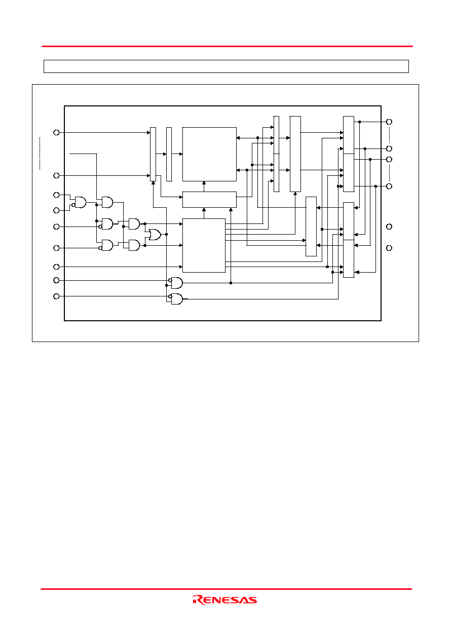
Block Diagram
Memory Array
1048576 Words
x 16BITS
OR
2097152 Words
x 8BITS
DECODER
ADDRESS BUFFER
CLOCK
GENERATOR
x8/x16
SWITCHING
CIRCUIT
CS2
CS1#
LB#
UB#
A0
A19
WE#
OE#
BYTE#
SENSE Amp.
SENSE Amp.
OUTPUT BUFFER
DATA INPUT
BUFFER
OUTPUT BUFFER
DATA INPUT
BUFFER
DQ0
DQ7
DQ8
DQ15
/ A-1
Vcc
Vss
DATA SELECTOR
DATA SELECTOR
R1LV1616R Series
Rev.1.00
2004.04.13
page 5 of 16
Note 1. -2.0V in case of AC (Pulse width
30ns)
2. Maximum voltage is +4.6V
Note 1. H:VIH L:VIL X: VIH or VIL
2. BYTE# pin supported by only TSOP type. When apply BYTE# ="L" , please assign LB#=UB#="L".
Operating Table
Absolute Maximum Ratings
Read
A-1
High-Z
Dout
L
H
L
L
L
H
L
Write
A-1
High-Z
Din
X
L
L
L
L
H
L
Read
Dout
Dout
Dout
L
H
L
L
H
H
L
Write
Din
Din
Din
X
L
L
L
H
H
L
Read from upper byte
Dout
Dout
High-Z
L
H
L
H
H
H
L
Write in upper byte
Din
Din
High-Z
X
L
L
H
H
H
L
Output disable
High-Z
High-Z
High-Z
H
H
X
X
X
H
L
Read from lower byte
High-Z
High-Z
Dout
L
H
H
L
H
H
L
Write in lower byte
High-Z
High-Z
Din
X
L
H
L
H
H
L
Stand by
High-Z
High-Z
High-Z
X
X
H
H
H
X
X
Stand by
High-Z
High-Z
High-Z
X
X
X
X
X
L
X
Stand by
High-Z
High-Z
High-Z
X
X
X
X
X
X
H
Operation
DQ15
DQ8-14
DQ0-7
OE#
WE#
UB#
LB#
BYTE#
CS2
CS1#
-40 to +85
-20 to +85
0 to +70
∫C
I ver.
∫C
W ver.
-40 to +85
-20 to +85
0 to +70
∫C
I ver.
∫C
W ver.
∫C
R ver.
Tbias
Storage temperature range under bias
∫C
-65 to +150
Tstg
Storage temperature
∫C
R ver.
Topr
Operation temperature
W
0.7
P
T
Power dissipation
V
-0.5*
1
to Vcc+0.3*
2
V
T
Terminal voltage on any pin relation toVss
V
-0.5 to +4.6
Vcc
Power supply voltage relative to Vss
Unit
Value
Symbol
Parameter

R1LV1616R Series
Rev.1.00
2004.04.13
page 6 of 16
Note 1. Typical parameter indicates the value for the center of distribution at 3.0V (Ta= 25
∫C
), and not 100% tested.
2. BYTE# pin supported by only TSOP type.
BYTE#
Vcc-0.2V or BYTE#
0.2V
Recommended Operating Conditions
DC Characteristics
I ver.
W ver.
R ver.
2
∫C
+85
-
-40
2
∫C
+85
-
-20
2
∫C
+70
-
0
Ta
Ambient temperature range
1
V
0.4
-
-0.2
V
IL
Input low voltage
V
Vcc+0.2
-
2.4
V
IH
Input high voltage
V
0
0
0
Vss
V
3.6
3.0
2.7
Vcc
Supply voltage
Note
Unit
Max.
Typ.
Min.
Symbol
Parameter
~+85∫C
µA
40
-
-
I
OL
= 2mA
V
0.4
-
-
V
OL
Output Low voltage
I
OH
= -1mA
V
-
-
2.4
V
OH
Output hige voltage
V in
0V
(1) 0V
CS2
0.2V or
(2) CS2
Vcc-0.2V,
CS1#
Vcc-0.2V or
(3)LB# =UB#
Vcc-0.2V,
CS2
Vcc-0.2V,
CS1#
0.2V
Average value
~+70∫C
µA
25
-
-
~+40∫C
µA
12
4
-
~+25∫C
µA
6
2
-
I
SB1
Standby current
CS2=V
IL
mA
0.3
0.1
-
I
SB
Standby current
mA
15
10
-
Icc
2
Read
Cycle time = 1 µs,
I
I/O
= 0 mA,
CS1#
0.2V, CS2
V
CC
-0.2V
V
IH
V
CC
-0.2V , V
IL
0.2V,
Write & Read duty=100%
respectively
mA
20
15
-
Icc
2
Write
Min. cycle, duty =100%
I
I/O
= 0 mA, CS1# =V
IL
,
CS2=V
IH
Others = V
IH
/ V
IL
mA
55
45
-
Icc
1
Average operating
current
CS1# =V
IH or
CS2=V
IL or
OE# = V
IH
or WE# =V
IL
or
LB# =UB# =V
IH,
V
I/O
=Vss to Vcc
µA
1
-
-
|I
Lo
|
Output leakage current
Vin=Vss to Vcc
µA
1
-
-
|I
LI
|
Input leakage current
Test conditions
*2
Unit
Max.
Typ.
*1
Min.
Symbol
Parameter
Note 1. ≠2.0V in case of AC (Pulse width
30ns)
2. Ambient
temperature range depends on R/W/I-version. Please see table on page 2.

R1LV1616R Series
Rev.1.00
2004.04.13
page 7 of 16
Capacitance
AC Characteristics
∑ Input pulse levels: VIL= 0.4V,VIH=2.4V
∑ Input rise and fall time : 5ns
∑ Input and output timing reference levels : 1.4V
∑ Output load : See figures (Including scope and jig)
Note 1:This parameter is sampled and not 100% tested.
1
V
I/O
= 0V
pF
10
-
-
C
I/O
Input / output capacitance
1
V in = 0V
pF
10
-
-
C in
Input capacitance
Note
Test conditions
Unit
Max.
Typ.
Min.
Symbol
Parameter
(Ta = +25∫C, f =1MHz)
CL=30pF
RL=500
DQ
1.4V
Test Conditions (Vcc=2.7~3.6V, Ta = 0~+70∫C / -20~+85∫C / -40~+85∫C *)
Note: Temperature range depends on R/W/I-version. Please see table on page 2.
R1LV1616R Series
Rev.1.00
2004.04.13
page 8 of 16
Read Cycle
1,2,3
ns
30
0
25
0
t
OHZ
Output disable to output in high-Z
1,2,3
ns
30
0
25
0
t
BHZ
LB#,UB# disable to high-Z
1,2,3
ns
30
0
25
0
t
CHZ2
1,2,3
ns
30
0
25
0
t
CHZ1
Chip deselect to output in high-Z
2,3
ns
-
5
-
5
t
OLZ
Output enable to output in low-Z
2,3
ns
-
5
-
5
t
BLZ
LB#,UB# enable to low-Z
2,3
ns
-
10
-
10
t
CLZ
Chip select to output in low-Z
ns
85
-
70
-
t
BA
LB#,UB# access time
ns
-
10
-
10
t
OH
Output hold from address change
ns
45
-
35
-
t
OE
Output enable to output valid
ns
85
-
70
-
t
ACS2
ns
85
-
70
-
t
ACS1
Chip select access time
ns
85
-
70
-
t
AA
Address access time
ns
-
85
-
70
t
RC
Read cycle time
Max.
Min.
Max.
Min.
Notes
Unit
R1LV1616R**-8S
R1LV1616R**-7S
Symbol
Parameter

R1LV1616R Series
Rev.1.00
2004.04.13
page 9 of 16
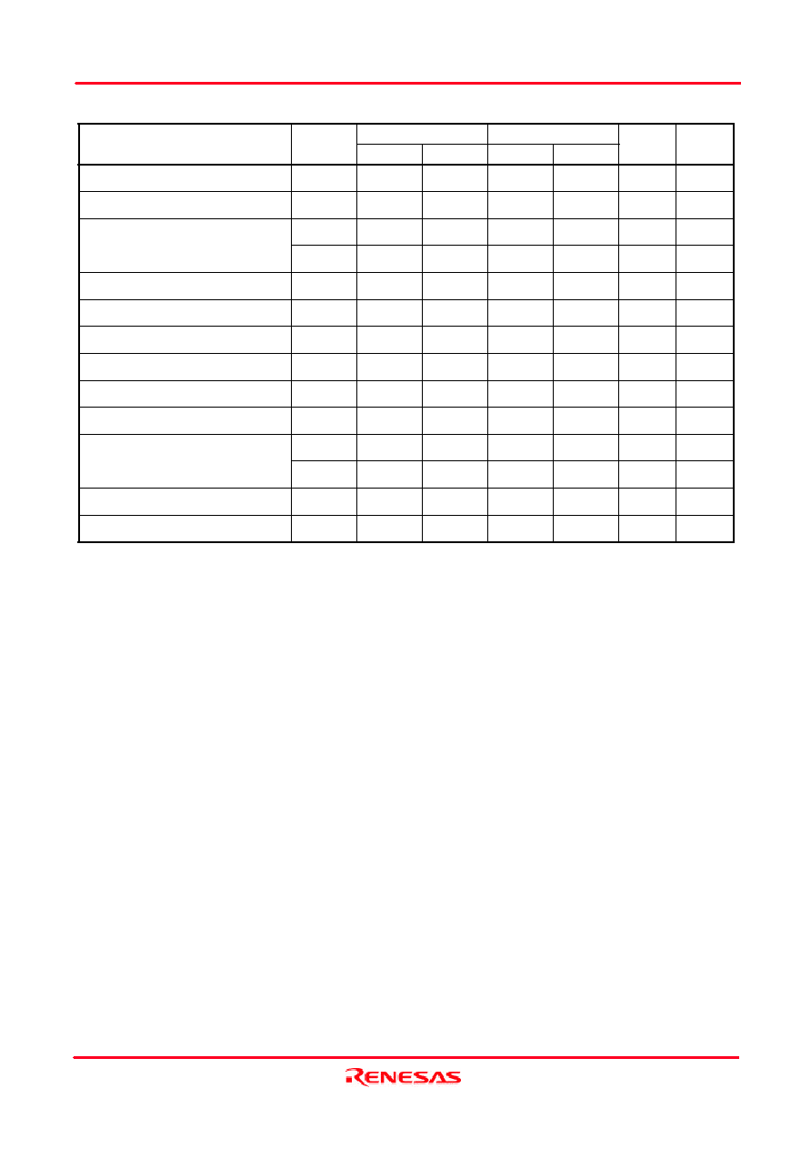
Write Cycle
Note
1
.
t
CHZ,
t
OHZ,
t
WHZ
and
t
BHZ
are defined as the time at which the outputs achieve the open circuit conditions
and are not referred to output voltage levels.
2. This parameter is sampled and not 100% tested.
3. AT any given temperature and voltage condition,
t
HZ
max is less than
t
LZ
min both for a given device and
form device to device.
4. A write occurs during the overlap of a low CS1#, a high CS2, a low WE# and a low LB# or a low UB#.
A write begins at the latest transition among CS1# going low, CS2 going high, WE# going low and LB#
going low or UB# going low .
A write ends at the earliest transition among CS1# going high, CS2 going low, WE# going high and LB#
going high or UB# going high.
t
WP
is measured from the beginning of write to the end of write.
5.
t
CW
is measured from the later of CS1# going low or CS2 going high to end of write.
6.
t
AS
is measured the address valid to the beginning of write.
7.
t
WR
is measured from the earliest of CS1# or WE# going high or CS2 going low to the end of write cycle.
1,2
ns
30
0
25
0
t
WHZ
Write to output in high-Z
Write pulse width
1,2
ns
30
0
25
0
t
OHZ
Output disable to output in high-Z
2
ns
-
5
-
5
t
OW
Output active from end of write
ns
-
0
-
0
t
DH
Data hold from write time
ns
-
40
-
35
t
DW
Data to write time overlap
7
ns
-
0
-
0
t
WR
Write recovery time
6
ns
-
0
-
0
t
AS
Address setup time
ns
-
70
-
65
t
BW
LB#,UB# valid to end of write
4
ns
-
60
-
55
t
WP
5
ns
-
70
-
65
t
CW
Chip selection to end of write
ns
-
70
-
65
t
AW
Address valid to end of write
ns
-
85
-
70
t
WC
Write cycle time
Max.
Min.
Max.
Min.
Notes
Unit
R1LV1616R**-8S
R1LV1616R**-7S
Symbol
Parameter
R1LV1616R Series
Rev.1.00
2004.04.13
page 10 of 16
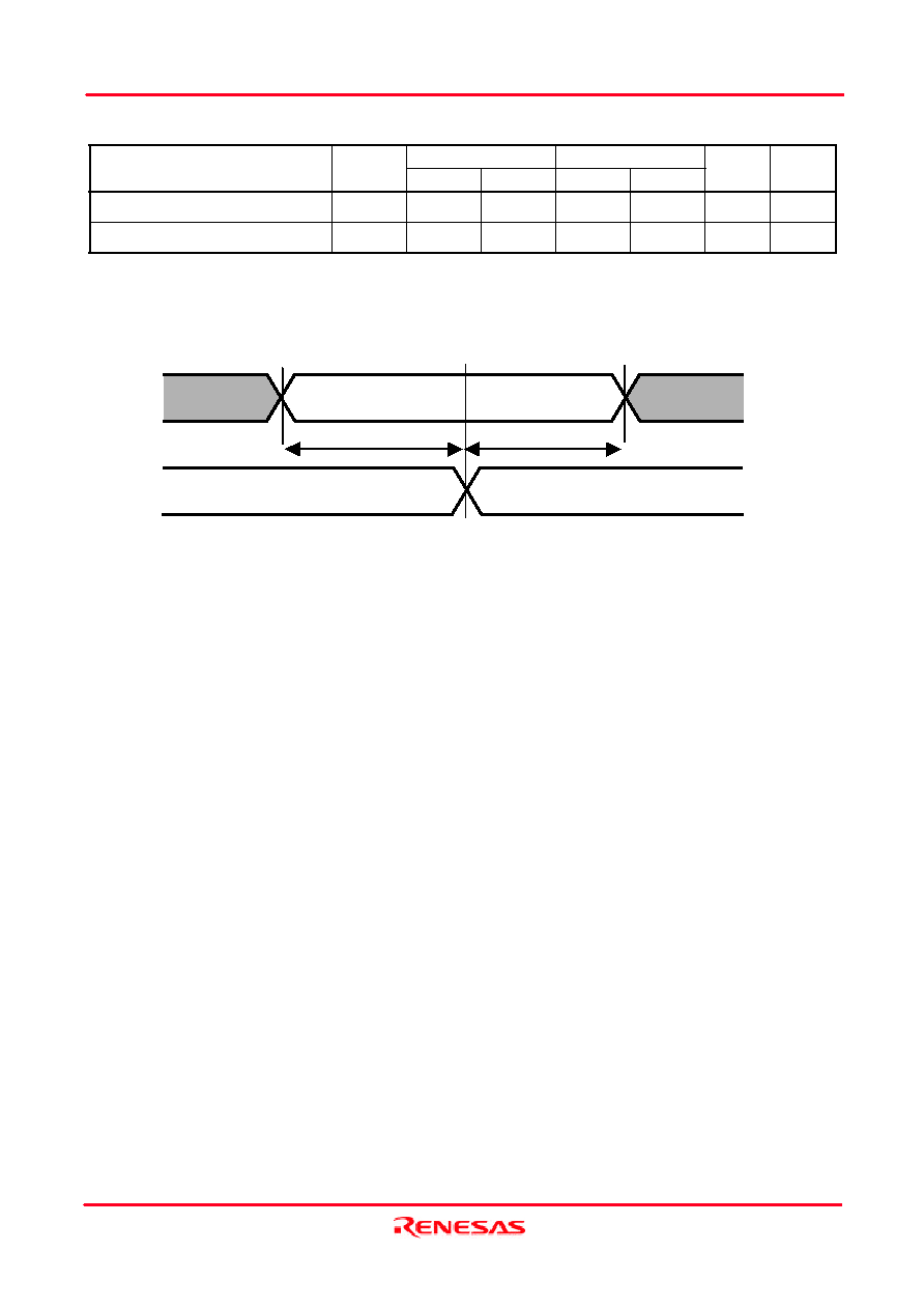
Byte enable (
supported by only
52-pin µTSOP )
BYTE# Timing Waveform
t
BS
BYTE#
CS1#
t
BR
CS2
ms
-
5
-
5
t
BR
Byte recovery time
ms
-
5
-
5
t
BS
Byte setup time
Max.
Min.
Max.
Min.
Notes
Unit
R1LV1616R**-8S
R1LV1616R**-7S
Symbol
Parameter
R1LV1616R Series
Rev.1.00
2004.04.13
page 11 of 16
Timing Waveform
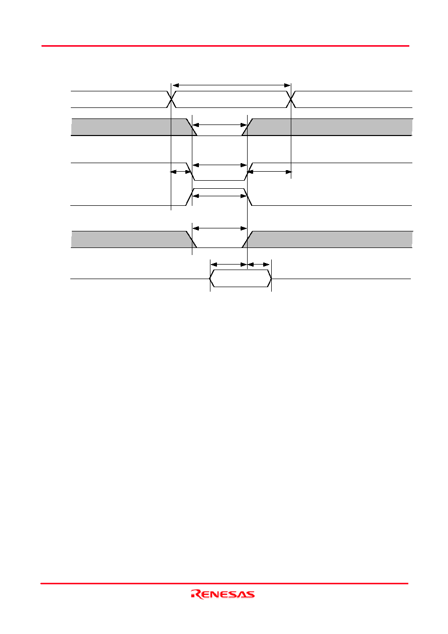
Read Cycle
LB#,UB#
A
0~19
(Word Mode)
A
-1~19
(Byte Mode)
DQ
0~15
(Word Mode)
DQ
0~7
(Byte Mode)
t
AA
WE# = "H" level
OE#
Valid data
CS1#
CS2
t
ACS1
t
BA
t
CLZ
t
BLZ
t
OE
t
OLZ
t
OHZ
t
CHZ1
t
BHZ
t
OH
Valid address
t
ACS2
t
CHZ2
t
RC
R1LV1616R Series
Rev.1.00
2004.04.13
page 12 of 16
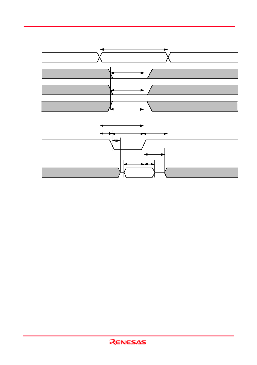
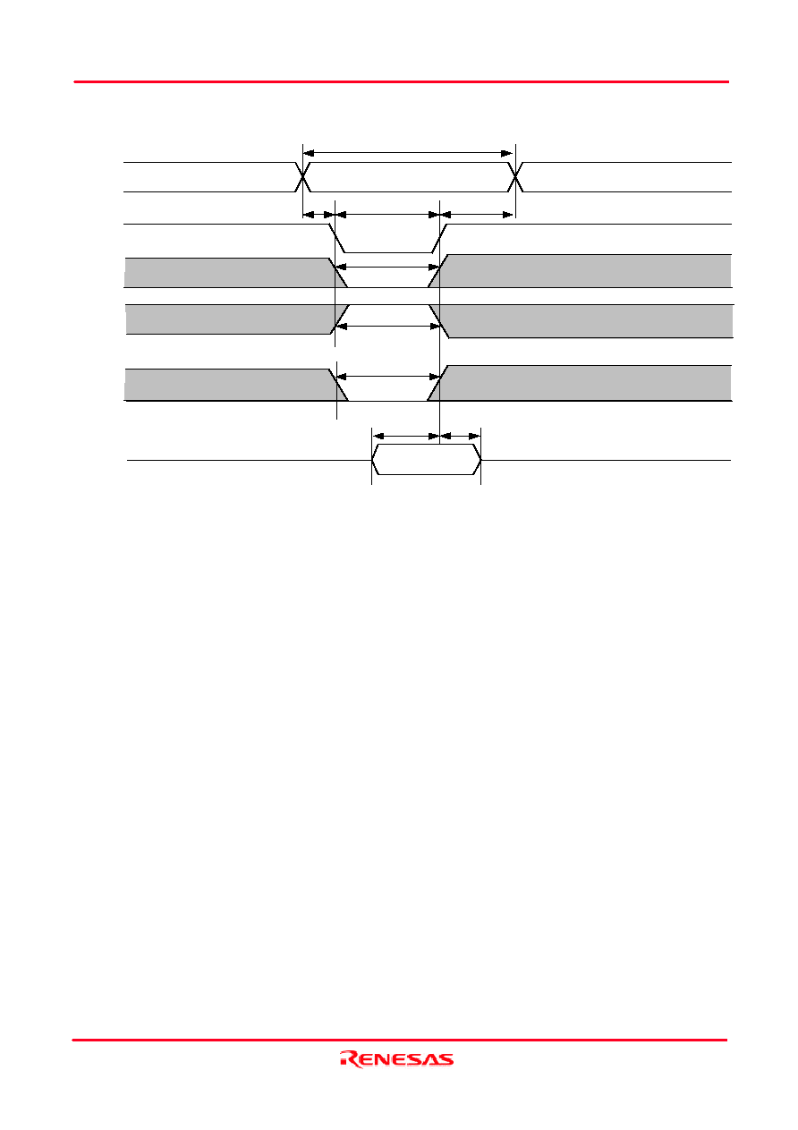
Write Cycle (1) (WE# Clock)
t
WC
A
0~19
(Word Mode)
A
-1~19
(Byte Mode)
DQ
0~15
(Word Mode)
DQ
0~7
(Byte Mode)
LB#,UB#
WE#
CS1#
CS2
t
CW
t
BW
t
AS
t
AW
t
WP
t
WHZ
t
OW
t
DW
t
WR
Valid data
Valid address
t
CW
t
DH
R1LV1616R Series
Rev.1.00
2004.04.13
page 13 of 16
Write Cycle (2) (CS1# ,CS2 Clock, OE#=V
IH
)
A
0~19
(Word Mode)
A
-1~19
(Byte Mode)
Valid data
DQ
0~15
(Word Mode)
DQ
0~7
(Byte Mode)
WE#
CS1#
CS2
t
AS
t
BW
t
WR
LB#,UB#
t
CW
t
WP
t
DW
t
DH
Valid address
t
CW
t
WC
R1LV1616R Series
Rev.1.00
2004.04.13
page 14 of 16
Write Cycle (3) ( LB#,UB# Clock, OE#=V
IH
)
t
WC
A
0~19
(Word Mode)
A
-1~19
(Byte Mode)
DQ
0~15
(Word Mode)
DQ
0~7
(Byte Mode)
WE#
CS1#
CS2
LB#,UB#
Valid data
t
AS
t
BW
t
WR
t
CW
t
WP
t
DW
t
DH
Valid address
t
CW

R1LV1616R Series
Rev.1.00
2004.04.13
page 15 of 16
Data Retention Characteristics
Note 1. Typical parameter of
Icc
DR
indicates the value for the center of distribution at Vcc=3.0V and not 100% tested.
2. BYTE# pin supported by TSOP type. BYTE#
Vcc-0.2V or BYTE#
0.2V
3. Also CS2 controls address buffer, WE# buffer ,CS1# buffer ,OE# buffer ,LB# ,UB# buffer and Din buffer .If CS2
controls data retention mode,Vin levels (address, WE# ,OE#,CS1#,LB#,UB#,I/O) can be in the high impedance
state. If CS1# controls data retention mode, CS2 must be CS2
Vcc-0.2V or 0V
CS2
0.2V. The other input
levels (address, WE# ,OE#,CS1#,LB#,UB#,I/O) can be in the high impedance state.
Data Retention timing Waveform (1) (LB#,UB# Controlled)
Data Retention timing Waveform (2) (CS1# Controlled)
Data Retention timing Waveform (3) (CS2 Controlled)
LB#
UB#
Vcc
t
CDR
t
R
2.4V
2.4V
2.70V
LB# =UB#
Vcc-0.2V
CS2
Vcc
t
CDR
t
R
0.2V
0.2V
2.70V
0V
CS2
0.2V
Vcc
CS1#
t
CDR
t
R
2.4V
2.4V
2.70V
CS1#
Vcc-0.2V
~+85∫C
µA
40
-
-
ms
-
-
5
t
R
Operation recovery time
See retention waveform
ns
-
-
0
t
CDR
Chip deselect to data retention time
~+70∫C
µA
25
-
-
~+40∫C
µA
12
4
-
Vcc=3.0V,Vin
0V
(1) 0V
CS2
0.2V or
(2) CS2
Vcc-0.2V,
CS1#
Vcc-0.2V or
(3) LB# =UB#
Vcc-0.2V,
CS2
Vcc-0.2V,
CS1#
0.2V
Average value
Test conditions
*2,3
Unit
Typ.
*1
~+25∫C
µA
6
2
-
Icc
DR
Data retention current
V in
0V
(1) 0V
CS2
0.2V or
(2) CS2
Vcc-0.2V,
CS1#
Vcc-0.2V or
(3) LB# =UB#
Vcc-0.2V,
CS2
Vcc-0.2V,
CS1#
0.2V
V
3.6
-
2.0
V
DR
Vcc for data retention
Max.
MIn.
Symbol
Parameter
R1LV1616R Series
Rev.1.00
2004.04.13
page 16 of 16
Sales Strategic Planning Div. Nippon Bldg., 2-6-2, Ohte-machi, Chiyoda-ku, Tokyo 100-0004, Japan
Copyright © 2004. Renesas Technology Corporation, All rights reserved. Printed in Japan.
http://www.renesas.com
Keep safety first in your circuit designs!
1. Renesas Technology Corporation puts the maximum effort into making semiconductor products better and more reliable, but there is always the possibility that trouble may occur with
them. Trouble with semiconductors may lead to personal injury, fire or property damage.
Remember to give due consideration to safety when making your circuit designs, with appropriate measures such as (i) placement of substitutive, auxiliary circuits, (ii) use of
nonflammable material or (iii) prevention against any malfunction or mishap.
Notes regarding these materials
1. These materials are intended as a reference to assist our customers in the selection of the Renesas Technology Corporation product best suited to the customer's application; they
do not convey any license under any intellectual property rights, or any other rights, belonging to Renesas Technology Corporation or a third party.
2. Renesas Technology Corporation assumes no responsibility for any damage, or infringement of any third-party's rights, originating in the use of any product data, diagrams, charts,
programs, algorithms, or circuit application examples contained in these materials.
3. All information contained in these materials, including product data, diagrams, charts, programs and algorithms represents information on products at the time of publication of these
materials, and are subject to change by Renesas Technology Corporation without notice due to product improvements or other reasons. It is therefore recommended that customers
contact Renesas Technology Corporation or an authorized Renesas Technology Corporation product distributor for the latest product information before purchasing a product listed
herein.
The information described here may contain technical inaccuracies or typographical errors.
Renesas Technology Corporation assumes no responsibility for any damage, liability, or other loss rising from these inaccuracies or errors.
Please also pay attention to information published by Renesas Technology Corporation by various means, including the Renesas Technology Corporation Semiconductor home page
(http://www.renesas.com).
4. When using any or all of the information contained in these materials, including product data, diagrams, charts, programs, and algorithms, please be sure to evaluate all information
as a total system before making a final decision on the applicability of the information and products. Renesas Technology Corporation assumes no responsibility for any damage,
liability or other loss resulting from the information contained herein.
5. Renesas Technology Corporation semiconductors are not designed or manufactured for use in a device or system that is used under circumstances in which human life is potentially
at stake. Please contact Renesas Technology Corporation or an authorized Renesas Technology Corporation product distributor when considering the use of a product contained
herein for any specific purposes, such as apparatus or systems for transportation, vehicular, medical, aerospace, nuclear, or undersea repeater use.
6. The prior written approval of Renesas Technology Corporation is necessary to reprint or reproduce in whole or in part these materials.
7. If these products or technologies are subject to the Japanese export control restrictions, they must be exported under a license from the Japanese government and cannot be
imported into a country other than the approved destination.
Any diversion or reexport contrary to the export control laws and regulations of Japan and/or the country of destination is prohibited.
8. Please contact Renesas Technology Corporation for further details on these materials or the products contained therein.