Rev.1.00, Mar.12.2004, page 1 of 12
R1RW0408D Series
4M High Speed SRAM (512-kword
◊
8-bit)
REJ03C0111-0100Z
Rev. 1.00
Mar.12.2004
Description
The R1RW0408D is a 4-Mbit high speed static RAM organized 512-kword
◊
8-bit. It has realized high
speed access time by employing CMOS process (6-transistor memory cell) and high speed circuit
designing technology. It is most appropriate for the application which requires high speed, high density
memory and wide bit width configuration, such as cache and buffer memory in system. The R1RW0408D
is packaged in 400-mil 36-pin SOJ for high density surface mounting.
Features
∑
Single supply: 3.3 V
±
0.3 V
∑
Access time: 12 ns (max)
∑
Completely static memory
No clock or timing strobe required
∑
Equal access and cycle times
∑
Directly TTL compatible
All inputs and outputs
∑
Operating current: 100 mA (max)
∑
TTL standby current: 40 mA (max)
∑
CMOS standby current : 5 mA (max)
: 0.8 mA (max) (L-version)
∑
Data retention current: 0.4 mA (max) (L-version)
∑
Data retention voltage: 2 V (min) (L-version)
∑
Center V
CC
and V
SS
type pin out
R1RW0408D Series
Rev.1.00, Mar.12.2004, page 2 of 12
Ordering Information
Type No.
Access time
Package
R1RW0408DGE-2PR
12 ns
400-mil 36-pin plastic SOJ (36P0K)
R1RW0408DGE-2LR 12
ns
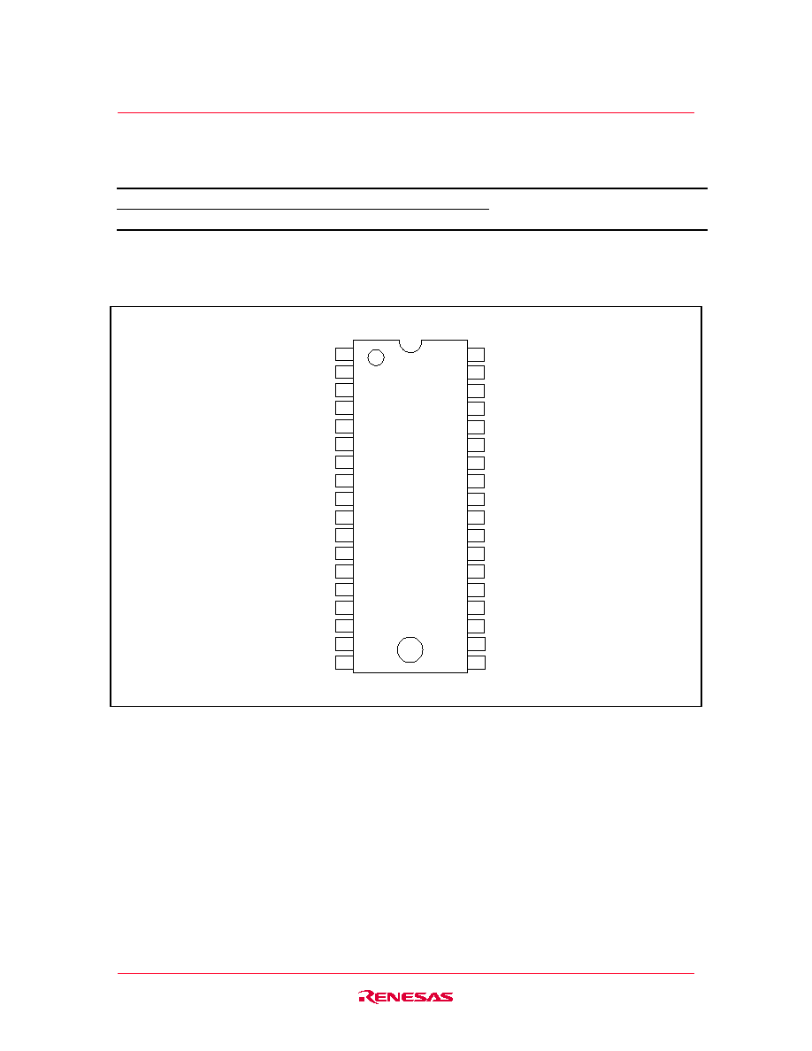
Pin Arrangement
1
2
3
4
5
6
7
8
9
10
11
12
13
14
15
16
17
18
36
35
34
33
32
31
30
29
28
27
26
25
24
23
22
21
20
19
A0
A1
A2
A3
A4
CS#
I/O1
I/O2
V
CC
V
SS
I/O3
I/O4
WE#
A5
A6
A7
A8
A9
NC
A18
A17
A16
A15
OE#
I/O8
I/O7
V
SS
V
CC
I/O6
I/O5
A14
A13
A12
A11
A10
NC
(Top View)
36-pin SOJ
R1RW0408D Series
Rev.1.00, Mar.12.2004, page 4 of 12
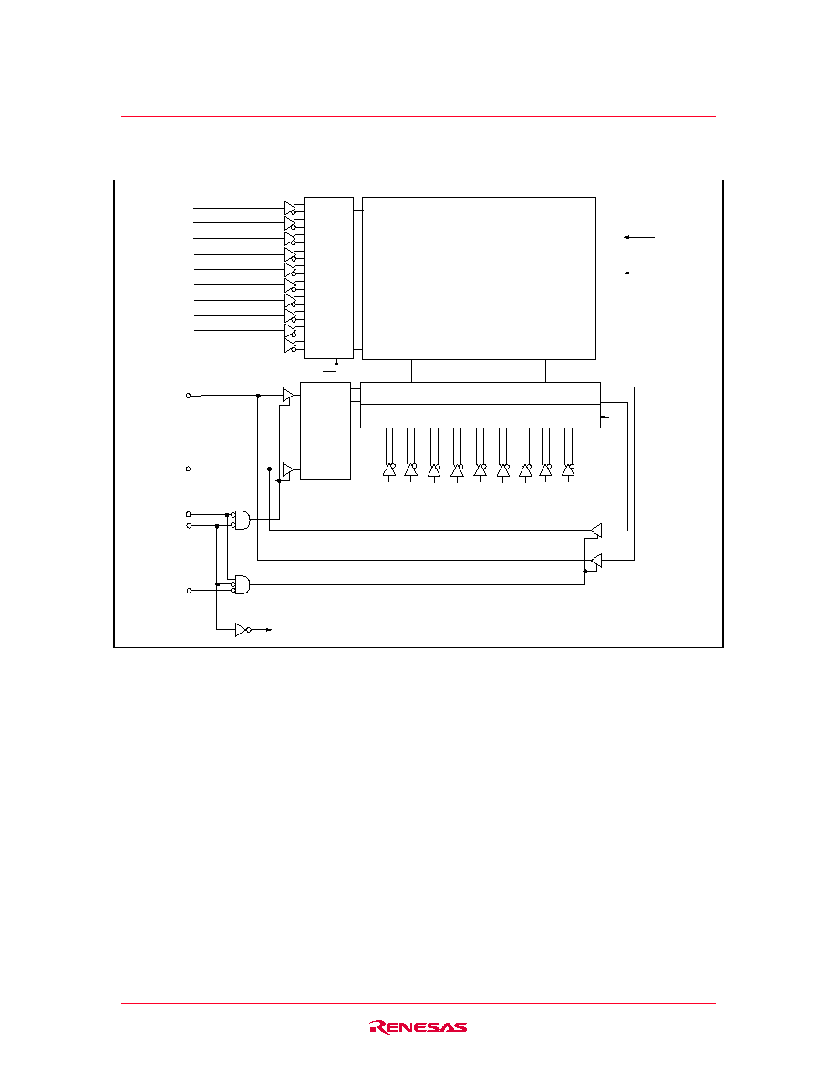
Block Diagram
I/O1
.
.
.
I/O8
WE#
Input
data
control
Column I/O
Column decoder
1024-row
◊
32-column
◊
16-block
◊
8-bit
(4,194,304 bits)
Row
decoder
OE#
CS#
CS
CS
V
CC
V
SS
CS
A14
A13
A12
A5
A6
A7
A11
A10
A3
A1
A8 A9 A18 A16 A17 A0 A2 A4 A15
(LSB)
(MSB)
(LSB)
(MSB)
R1RW0408D Series
Rev.1.00, Mar.12.2004, page 5 of 12
Operation Table
CS# OE# WE# Mode
V
CC
current
I/O
Ref. cycle
H
◊
◊
Standby I
SB
, I
SB1
High-Z
L H H Output
disable
I
CC
High-Z
L L H Read
I
CC
D
OUT
Read cycle (1) to (3)
L H L Write
I
CC
D
IN
Write cycle (1)
L L L Write
I
CC
D
IN
Write cycle (2)
Note: H: V
IH
, L: V
IL
,
◊
: V
IH
or V
IL
Absolute Maximum Ratings
Parameter Symbol
Value
Unit
Supply voltage relative to V
SS
V
CC
-
0.5 to +4.6
V
Voltage on any pin relative to V
SS
V
T
-
0.5
*
1
to V
CC
+ 0.5
*
2
V
Power dissipation
P
T
1.0
W
Operating temperature
Topr
0 to +70
∞
C
Storage temperature
Tstg
-
55 to +125
∞
C
Storage temperature under bias
Tbias
-
10 to +85
∞
C
Notes: 1. V
T
(min) =
-
2.0 V for pulse width (under shoot)
6 ns.
2.
V
T
(max) = V
CC
+ 2.0 V for pulse width (over shoot)
6 ns.
Recommended DC Operating Conditions
(Ta = 0 to +70
∞
C)
Parameter Symbol
Min
Typ
Max
Unit
Supply voltage
V
CC
*
3
3.0 3.3 3.6 V
V
SS
*
4
0 0 0 V
Input voltage
V
IH
2.0
V
CC
+ 0.5
*
2
V
V
IL
-
0.5
*
1
0.8 V
Notes: 1. V
IL
(min) =
-
2.0 V for pulse width (under shoot)
6 ns.
2.
V
IH
(max) = V
CC
+ 2.0 V for pulse width (over shoot)
6 ns.
3. The supply voltage with all V
CC
pins must be on the same level.
4. The supply voltage with all V
SS
pins must be on the same level.