Rev.1.00
2004.4.13
page 1 of 16
REJ03C0215-0100Z
Rev.1.00
2004.4.13
R1W V3216R Series
32Mb superSRAM (2M wordx16bit)
Description
Features
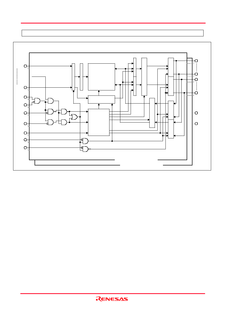
The R1WV3216R Series is a family of low voltage 32-Mbit static RAMs organized as 2097152-words by 16-bit,
fabricated by Renesas's high-performance 0.15um CMOS and TFT technologies.
The R1WV3216R Series is suitable for memory applications where a simple interfacing , battery operating and
battery backup are the important design objectives.
The R1WV3216R Series is made by stacked-micro-package technology and two chips of 16Mbit superSRAMs
are assembled in one package.
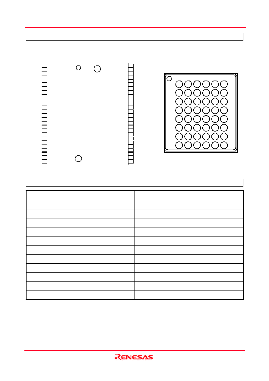
The R1WV3216R Series is packaged in a 52pin micro thin small outline mount device[
µ
TSOP / 10.79mm x
10.49mm with the pin-pitch of 0.4mm] or a 48balls fine pitch ball grid array [f-BGA / 7.5mmx8.5mm with the ball-pitch
of 0.75mm and 6x8 array] . It gives the best solution for a compaction of mounting area as well as flexibility of wiring
pattern of printed circuit boards.
∑ Single 2.7-3.6V power supply
∑ Small stand-by current:4
µ
A (3.0V, typ.)
∑ Data retention supply voltage =2.0V
∑ No clocks, No refresh
∑ All inputs and outputs are TTL compatible.
∑ Easy memory expansion by CS1#, CS2, LB# and UB#
∑ Common Data I/O
∑ Three-state outputs: OR-tie capability
∑ OE# prevents data contention on the I/O bus
∑ Process technology: 0.15um CMOS

R1W V3216R Series
Rev.1.00
2004.4.13
page 2 of 16
Ordering Information
85 ns
R1WV3216RBG-8S%
7.5mmx8.5mm f-BGA 0.75mm pitch 48ball
70 ns
R1WV3216RBG-7S%
85 ns
R1WV3216RSD-8S%
350-mil 52-pin plastic µ - TSOP(II)
(normal-bend type) (52PTG)
70 ns
R1WV3216RSD-7S%
Package
Access time
Type No.
% - Temperature version; see table below
-40 ~ +85 ∫C
I
-20 ~ +85 ∫C
W
0 ~ +70 ∫C
R
Temperature Range
%
R1W V3216R Series
Rev.1.00
2004.4.13
page 5 of 16
Operating Table
Absolute Maximum Ratings
Note 1: -2.0V in case of AC (Pulse width
30ns)
2:Maximum voltage is +4.6V
Read
A-1
High-Z
Dout
L
H
L
L
L
H
L
Write
A-1
High-Z
Din
X
L
L
L
L
H
L
Read
Dout
Dout
Dout
L
H
L
L
H
H
L
Write
Din
Din
Din
X
L
L
L
H
H
L
Read from upper byte
Dout
Dout
High-Z
L
H
L
H
H
H
L
Write in upper byte
Din
Din
High-Z
X
L
L
H
H
H
L
Output disable
High-Z
High-Z
High-Z
H
H
X
X
X
H
L
Read from lower byte
High-Z
High-Z
Dout
L
H
H
L
H
H
L
Write in lower byte
High-Z
High-Z
Din
X
L
H
L
H
H
L
Stand by
High-Z
High-Z
High-Z
X
X
H
H
H
X
X
Stand by
High-Z
High-Z
High-Z
X
X
X
X
X
L
X
Stand by
High-Z
High-Z
High-Z
X
X
X
X
X
X
H
Operation
DQ15
DQ8-14
DQ0-7
OE#
WE#
UB#
LB#
BYTE#
CS2
CS1#
Note 1. H:VIH L:VIL X: VIH or VIL
2. BYTE# pin supported by only TSOP type. When apply BYTE# ="L" , please assign LB#=UB#="L".
-40 to +85
-20 to +85
0 to +70
∫C
I ver.
∫C
W ver.
-40 to +85
-20 to +85
0 to +70
∫C
I ver.
∫C
W ver.
∫C
R ver.
Tbias
Storage temperature range under bias
∫C
-65 to +150
Tstg
Storage temperature
∫C
R ver.
Topr
Operation temperature
W
0.7
P
T
Power dissipation
V
-0.5*
1
to Vcc+0.3*
2
V
T
Terminal voltage on any pin relation toVss
V
-0.5 to +4.6
Vcc
Power supply voltage relative to Vss
Unit
Value
Symbol
Parameter