ChipFind - документация

Электронный компонент: R2S15903SP

Скачать:  PDF   ZIP
Rev.1.4 Dec 06, 2005 page 1 of 11
Preliminary
R2S15903SP
Sound Controller with Surround & AGC
REJ03F0159-0140
Rev.1.4
Dec 06, 2005
Description
The R2S15903SP is an optimum audio signal processor IC for TV. It has a 5ch input selector, AGC, surround/pseudo
stereo, tone control(2band), output gain control and 2ch master volume. It can control all of these functions with I
2
C
bus.
Features
Volume: 0 to 89dB, / 1dB step. Each channel is independence control.
5 input selector + MUTE
2 Rec output (0/2dB)
Auto gain control (AGC level 4step)
Tone control Bass: 15dB to +15dB/ 1dB step
Treble: 15dB to +15dB/ 1dB step
Surround <Low/ High>/ Pseudo stereo
Mode selector: Bypass/ Tone / Tone & Pseudo Stereo or Surround
Output gain control: 0dB/ +4.5dB
I
2
C-BUS control
Recommended Operating Condition
Supply voltage: V
CC
= 9.0V(typ)
Application
TV, Mini Stereo, etc.
System Configuration
ROUT
LOUT
I C-BUS I/F
IN R2
IN R3
REC R1
(IN R4)
SDA
R2S15903SP
Pseudo Stereo
and
Surround
Tone Control
(Bass / Treble)
Mode selector
Mode Selector
SCL
Volume L
Volume R
IN R1
REC R2
(IN R5)
IN L2
IN L1
REC L1
(IN L4)
IN L3
REC L2
(IN L5)
Output Gain
Control
Output Gain
Control
VCC=9V
AGC
2
R2S15903SP
Preliminary
Rev.1.4 Dec 06, 2005 page 2 of 11
Block Diagram and Pin Configuration
REFIN
INL1
INL2
INL3
CAGC1
AGCLOUT
VOLINL
VCC
INR1
INR2
INR3
CAGC2
AGCROUT
VOLINR
TRER
BASSL2
BASSL2
BASSR2
BASSR2
RECL1
(INL4)
RECL2
(INL5)
TREL
RECR1
(INR4)
RECR2
(INR5)
ROUT
GND
LOUT
PSEUDO
SCL
SDA
Rext
Cext
32
31
30
29
28
27
26
25
24
23
1
2
3
4
5
6
7
8
9
10
22
21
11
12
Mode
Selector
Input
Selector
Pseudo
Stereo
and
Surround
REF
Lch Volume
0~-89dB,-
Rch Volume
Input
Selector
Output
Gain
Control
Output
Gain
Control
0/-2dB
0/-2dB
13
14
20
19
De-pop
15
16
18
17
AGC
I C-BUS
I/F
Mode
Selector
+
-
+ -
+
-
2
0~-89dB,-
Tone Control
Bass/ Treble
Tone Control
Bass/ Treble
R2S15903SP
Preliminary
Rev.1.4 Dec 06, 2005 page 3 of 11
Application Example
INL1
LOUT
ROUT
MCU
SCL
SDA
INL2
INL3
RECL1
(INL4)
RECL2
(INL5)
1F
1F
1F
1F
4.7F
4.7F
8200pF
0.068F
0.068F
8.2k
0.015F
47k
4.7F
0.22F
10k
1F
INR1
1F
INR2
1F
INR3
4.7F
RECR1
(INR4)
4.7F
RECR2
(INR5)
VCC=9V
47k
4.7F
32
31
30
29
28
27
26
25
24
23
1
2
3
4
5
6
7
8
9
10
22
21
11
12
Mode
Selector
Input
Selector
Pseudo
Stereo
and
Surround
REF
Lch Volume
0~-89dB,-
Rch Volume
0~-89dB,-
Input
Selector
Tone Control
Bass/ Treble
Output
Gain
Control
Output
Gain
Control
13
14
20
19
De-pop
15
16
18
17
AGC
I C-BUS
I/F
0.068F
0.068F
8.2k
8200pF
1F
1M
33F
2.2F
2.2F
Mode
Selector
+
+
+
+
+
+
+
+
+
+
-
+ -
+
-
+
+
+
+
+
+
+
+
2
Tone Control
Bass/ Treble
0/-2dB
0/-2dB
R2S15903SP
Preliminary
Rev.1.4 Dec 06, 2005 page 4 of 11
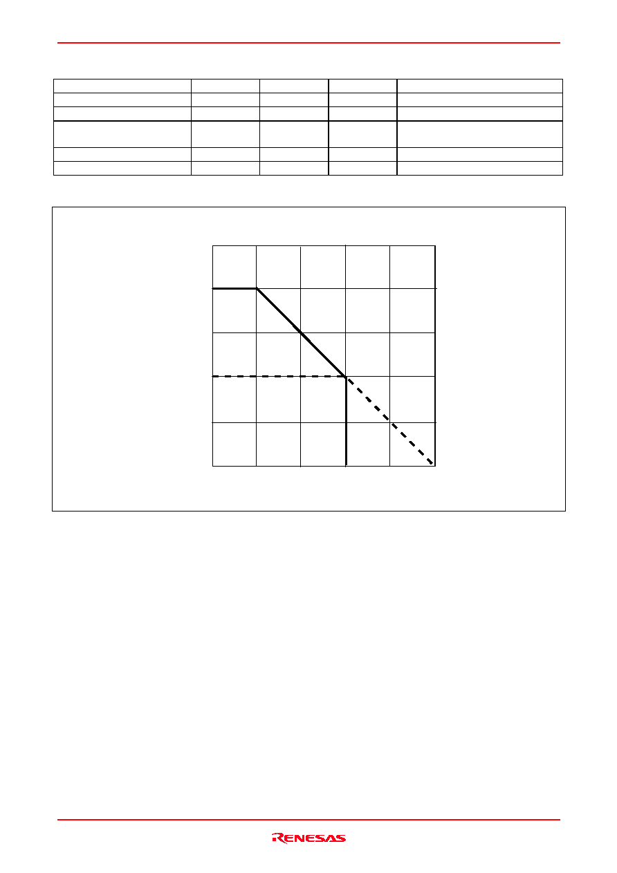
Absolute Maximum Ratings
Parameter
Symbol
Ratings
Unit
Condition
Power supply
V
CC
10
V
Power dissipation
Pd
1.0
W
Ta
25C
Thermal derating
K
10.0
mW/C
Ta>25C
(Circuit board installation)
Operating temperature
Topr
20 to +75
C
Storage temperature
Tstg
40 to +125
C

25
50
75
100
125
0.25
0.5
0.75
1.0
1.25
THERMAL DERATINGS
(MAXIMUM RATING)
AMBIENT TEMPERATURE Ta (C)
POWER DISSIP
A
T
ION pd (W)
0
0
R2S15903SP
Preliminary
Rev.1.4 Dec 06, 2005 page 5 of 11
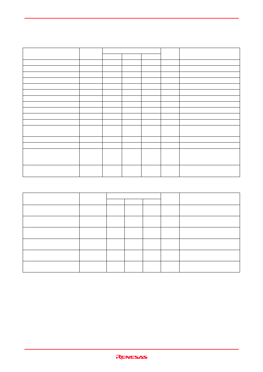
Electrical Characteristics
(V
CC
=9V, Ta=25C, Vi=100mVrms, f=1kHz, Bypass, AGC: off, Rg=0
, RL=47k, unless otherwise noted)
General Characteristics
Limits
Parameter
Symbol
Min Typ Max
Unit
Condition
Operational power supply
V
CC
8.0
9.0
9.7
V
Supply current
I
CC
--
25
35
mA
No
signal
Reference voltage
Vref
4.0
4.5
5.0
V
No signal
Input impedance
RIN
17
25
33
k
Maximum input voltage
VIM
2.8
3.0
--
Vrms
VOL=20dB, THD=3%
Maximum output voltage
VOM
--
2.5
--
Vrms
VOL=0dB, THD=1%
Rec output gain
Gvrec
--
0/ 2.0
--
dB
Rec out (0/ 2dB)
Output gain
Gvout
--
4.5
--
dB
Output gain=4.5dB
Volume maximum
VOLmax
2
0
+2
dB
VOL=0dB
Volume minimum
VOLmin
--
85
70
dB
VOL=Mute, Vin=1Vrms, IHF-A
Channel balance
CBAL
1.5
0
1.5
dB
VOL=0dB
Total harmonic distortion
THD
--
--
0.5
%
400Hz to 30kHz BPF
Vo=0.5Vrms
Input selector cross talk
CT
--
--
70
dB
Vin=1Vrms, IHF-A
Channel separation
CS
--
--
70
dB
Vin=1Vrms, IHF-A,
Output noise 1
Vno1
--
90
(31.6)
85
(56.2)
dBV
(Vrms)
VOL=0dB,Output gain=0dB
Tone=0dB,Surround ON,
AGC: OFF, IHF-A
Output noise 2
Vno2
--
103
(7)
97
(14)
dBV
(Vrms)
VOL=Mute, Output gain=0dB
Bypass, AGC: OFF, IHF-A
Tone Control
Limits
Parameter
Symbol
Min Typ Max
Unit
Condition
Tone control voltage gain
(Boost/Bass)
G (Bass) B
+12.5
+15
+17.5
dB
f = 100Hz
Bass= + 15dB
Tone control voltage gain
(Cut/Bass)
G (Bass) C
17.5
15
12.5
dB
f = 100Hz
Bass = 15dB
Tone control voltage gain
(Flat/Bass)
G (Bass) F
2
0
+2
dB
f = 100Hz
Bass = 0dB
Tone control voltage gain
(Boost/Treble)
G (Treble) B
+12.5
+15
+17.5
dB
f = 10kHz
Tre = +15dB
Tone control voltage gain
(Cut/Treble)
G (Treble) C
17.5
15
12.5
dB
f = 10kHz
Tre = 15dB
Tone control voltage gain
(Flat/Treble)
G (Treble) F
2
0
+2
dB
f = 100Hz
Tre = 0dB
R2S15903SP
Preliminary
Rev.1.4 Dec 06, 2005 page 6 of 11
AGC
Limits
Parameter
Symbol
Min Typ Max
Unit
Condition
AGC Boost
AGCBST
1.5
3.5
5.5
dB
AGC level = 300mVrms
Vin = 50mVrms, f = 1kHz
AGC FLAT1
AGCFLT1
2.5
0.0
2.5
dB
AGC level = 300mVrms
Vin = 300mVrms, f = 1kHz
AGC FLAT2
AGCFLT2
2.5
0.0
2.5
dB
AGC level = 400mVrms
Vin = 400mVrms, f = 1kHz
AGC FLAT3
AGCFLT3
2.5
0.0
2.5
dB
AGC level = 500mVrms
Vin = 500mVrms, f = 1kHz
AGC FLAT4
AGCFLT4
2.5
0.0
2.5
dB
AGC level = 600mVrms
Vin = 600mVrms, f = 1kHz
AGC CUT
AGCCUT
14
10
6.0
dB
AGC level = 300mVrms
Vin = 2Vrms, f = 1kHz
I
2
C BUS Interface
Limits
Parameter
Symbol
Min Typ Max
Unit
Condition
Low level input voltage
V
IL
0
--
1.5
V
V
CC
=9V
High level input voltage
V
IH
3
--
5
V
V
CC
=9V
Maximum clock frequency
f
SCL
100
kHz
R2S15903SP
Preliminary
Rev.1.4 Dec 06, 2005 page 7 of 11
Function Description
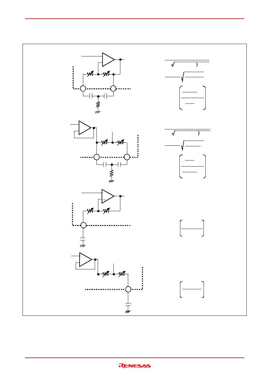
1. Tone Control Circuit
<1> Bass Circuit
OUT
IN
R2
R3
C2
C1
R1
fo =
2
R1(R2+R3 C1C2
1
( Hz)
Q ~
=
C1+C2
R1
1
(R3=0)
C1C2R2
Gv = 20 log
(dB)
R1
R3
+2
R1
R2+R3
+2
(C1=C2)
OUT
IN
R3
R2
C2
C1
R1
fo =
2
R1(R2+R3 C1C2
1
(Hz)
Q
C1+C2
R1
1
(R3=0)
C1C2R2
Gv = 20 log
(dB)
R1
+2
R3
R2+R3
R1
+2
(C1=C2)
OUT
IN
R2
R1
C
Gv = 20 log
(dB)
R1+R2
R1
OUT
IN
R1
R2
C
Gv = 20 log
(dB)
R1+R2
R1
~
=
Boost
Cut
<2> Treble Circuit
Boost
Cut
+
-
+
-
+
-
+
-
R2S15903SP
Preliminary
Rev.1.4 Dec 06, 2005 page 8 of 11
I
2
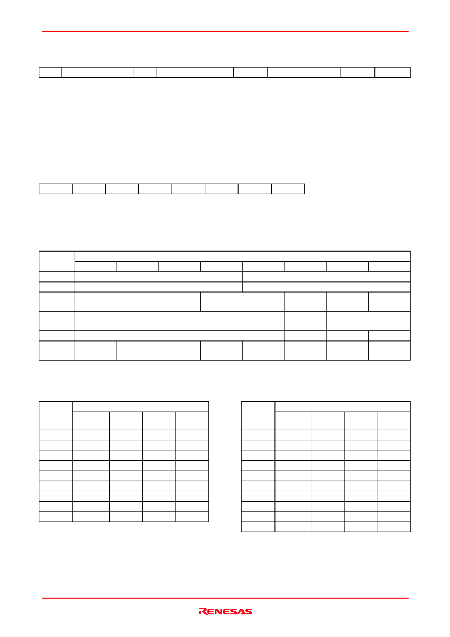
C Bus Format
MSB
LSB MSB
LSB
MSB
LSB
S Slave
Address A Sub
Address
A
Data
A P
1 bit
8bit
1 bit
8bit
1 bit
8bit
1 bit
1bit
S: Starting Term
A: Acknowledge Bit
P: Stop Term
If more than one Data Byte is transmitted, then the significant SUB ADDRESS bits are auto incremented.
00H
01H
02H
03H
04H
05H
00H
1. Slave Address
MSB
LSB
1 0 0 0 0 0 1
R/W
B
R/W
B
= 0: Write mode for register setting
R/W
B
= 1: Not available
2. Sub Address Table
BIT
Sub
address
D7 D6 D5 D4 D3 D2 D1 D0
00H
Lch VOL<H>
Lch VOL<L>
01H
Rch VOL<H>
Rch VOL<L>
02H Input
selector
Rec
output
Output
gain
Lch mute
Rch mute
03H Bass
Surround
level
Mode selector
04H Treble
Rec
gain
0
0
05H
AGC/
Bypass
AGC level
AGC
mode
0 0 0 0
3. Data Table
<1> Master Volume Control (Sub Address: 00H, 01H)
VOL<H>
VOL<L>
VOL
ATT
(dB)
D7 D6 D5 D4
VOL
ATT
(dB)
D3 D2 D1 D0
0 0 0 0 0 0 0 0 0 0
10 0 0 0 1 1 0 0 0 1
20 0 0 1 0 2 0 0 1 0
30 0 0 1 1 3 0 0 1 1
40 0 1 0 0 4 0 1 0 0
50 0 1 0 1 5 0 1 0 1
60 0 1 1 0 6 0 1 1 0
70 0 1 1 1 7 0 1 1 1
80 1 0 0 0 8 1 0 0 0
9
1 0 0 1
R2S15903SP
Preliminary
Rev.1.4 Dec 06, 2005 page 9 of 11
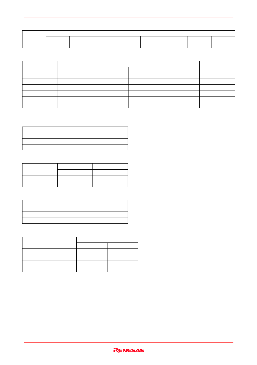
Example: If the volume of the Lch is set to 28dB, the Data byte is transmitted as follows:
BIT
Sub
address
D7 D6 D5 D4 D3 D2 D1 D0
00H
0 0 1 0 1 0 0 0
<2> Input Selector (Sub Address: 02H)
Input selector
REC1
REC2
Input
D7 D6 D5 D4 D3
All
OFF
0 0 0 A A
IN1 0 0 1 A A
IN2 0 1 0 A A
IN3 0 1 1 A A
IN4 1 0 0 1 A
IN5 1 0 1 A 1
If A=0 means REC1 or REC2 output ON, then A=1 means REC1 or REC2 output OFF.
<3> Output Gain (Sub Address: 02H)
Output gain
Gain
D2
0dB 0
+4.5dB 1
<4> Mute Function (Sub Address: 02H)
Lch Rch
Mute
D1 D0
Mute ON
0
0
Mute OFF
1
1
<5> Surround Mode (Sub Address: 03H)
Surround level
Surround level
D2
Low level
0
High level
1
<6> Mode Selector (Sub Address: 03H)
Mode selector
Mode
D1 D0
Bypass 0
0
Tone 0
1
Tone & Pseudo stereo
1
0
Tone & Surround
1
1
R2S15903SP
Preliminary
Rev.1.4 Dec 06, 2005 page 10 of 11
<7> Tone Control (Sub Address: 03H Bass, 04H Treble)
Bass/ Treble
Gain
(dB)
D7 D6 D5 D4 D3
0
0 0 0 0
1
0 0 0 1
2
0 0 1 0
3
0 0 1 1
4
0 1 0 0
5
0 1 0 1
6
0 1 1 0
7
0 1 1 1
8
1 0 0 0
9
1 0 0 1
10
1 0 1 0
11
1 0 1 1
12
1 1 0 0
13
1 1 0 1
14
1 1 1 0
15
A
1 1 1 1
If A=0 means Tone control gain CUT(), then A=1 means Tone control gain BOOST(+).
<8> AGC/ Bypass (Sub Address: 05H)
Mode selector
Mode
D7
Bypass 0
AGC 1
<9> AGC Level (Sub Address: 05H)
AGC level
AGC level
D6 D5
300mVrms 0
0
400mVrms 0
1
500mVrms 1
0
600mVrms 1
1
<10> AGC Mode (Sub Address: 05H)
AGC mode
AGC mode
D4
Limitation* 0
Always** 1
*: When input level is more than 10mVrms, AGC circuit works.
**: Regardless of input level, AGC circuit always works.
<11> REC Gain (Sub Address: 04H)
Rec gain
Gain
D2
0dB 0
2dB 1
R2S15903SP
Preliminary
Rev.1.4 Dec 06, 2005 page 11 of 11
Note
1. When power supply is turned on
Please do not transmit I
2
C data during 370ms when you turn on the power supply.
( Cext(16pin)=0.22
F , Rext(15-16pin)=10k )
power supply
V
CC
(9V)
V
CC
(5V)
Waiting interval
more than 370ms
Transmitting I C data
V
t
2
2. When mode is changed
Please do not transmit I
2
C data during 370ms when you change the mode selector.
( Cext(16pin)=0.22
F , Rext(15-16pin)=10k )
(EX .1) Bypass
Tone
S
Slave
A
A
Data
A P
Address
Sub
03H
Address
XXXXXX00
S
Slave
A
A
Data
A P
Address
Sub
03H
Address
XXXXXX01
Waiting interval
more than 370ms
(EX .2) Surround L
Surround H
S
Slave
A
A
Data
A P
Address
Sub
03H
Address
XXXXX011
S
Slave
A
A
Data
A P
Address
Sub
03H
Address
XXXXX111
Waiting interval
more than 370ms
When the TONE Bass gain is changed, waiting interval is unnecessary.
(EX .3) TONE Bass 1dB
2dB
S Slave
A
A
Data
A P
Address
Sub
03H
Address
10001001
S Slave
A
A
Data
A P
Address
Sub
03H
Address
10010001
No Waiting interval
Keep safety first in your circuit designs!
1. Renesas Technology Corp. puts the maximum effort into making semiconductor products better and more reliable, but there is always the possibility that trouble
may occur with them. Trouble with semiconductors may lead to personal injury, fire or property damage.
Remember to give due consideration to safety when making your circuit designs, with appropriate measures such as (i) placement of substitutive, auxiliary
circuits, (ii) use of nonflammable material or (iii) prevention against any malfunction or mishap.
Notes regarding these materials
1. These materials are intended as a reference to assist our customers in the selection of the Renesas Technology Corp. product best suited to the customer's
application; they do not convey any license under any intellectual property rights, or any other rights, belonging to Renesas Technology Corp. or a third party.
2. Renesas Technology Corp. assumes no responsibility for any damage, or infringement of any third-party's rights, originating in the use of any product data,
diagrams, charts, programs, algorithms, or circuit application examples contained in these materials.
3. All information contained in these materials, including product data, diagrams, charts, programs and algorithms represents information on products at the time of
publication of these materials, and are subject to change by Renesas Technology Corp. without notice due to product improvements or other reasons. It is
therefore recommended that customers contact Renesas Technology Corp. or an authorized Renesas Technology Corp. product distributor for the latest product
information before purchasing a product listed herein.
The information described here may contain technical inaccuracies or typographical errors.
Renesas Technology Corp. assumes no responsibility for any damage, liability, or other loss rising from these inaccuracies or errors.
Please also pay attention to information published by Renesas Technology Corp. by various means, including the Renesas Technology Corp. Semiconductor
home page (http://www.renesas.com).
4. When using any or all of the information contained in these materials, including product data, diagrams, charts, programs, and algorithms, please be sure to
evaluate all information as a total system before making a final decision on the applicability of the information and products. Renesas Technology Corp. assumes
no responsibility for any damage, liability or other loss resulting from the information contained herein.
5. Renesas Technology Corp. semiconductors are not designed or manufactured for use in a device or system that is used under circumstances in which human life
is potentially at stake. Please contact Renesas Technology Corp. or an authorized Renesas Technology Corp. product distributor when considering the use of a
product contained herein for any specific purposes, such as apparatus or systems for transportation, vehicular, medical, aerospace, nuclear, or undersea repeater
use.
6. The prior written approval of Renesas Technology Corp. is necessary to reprint or reproduce in whole or in part these materials.
7. If these products or technologies are subject to the Japanese export control restrictions, they must be exported under a license from the Japanese government and
cannot be imported into a country other than the approved destination.
Any diversion or reexport contrary to the export control laws and regulations of Japan and/or the country of destination is prohibited.
8. Please contact Renesas Technology Corp. for further details on these materials or the products contained therein.
Sales Strategic Planning Div. Nippon Bldg., 2-6-2, Ohte-machi, Chiyoda-ku, Tokyo 100-0004, Japan
http://www.renesas.com
Refer to "http://www.renesas.com/en/network" for the latest and detailed information.
Renesas Technology America, Inc.
450 Holger Way, San Jose, CA 95134-1368, U.S.A
Tel: <1> (408) 382-7500, Fax: <1> (408) 382-7501
Renesas Technology Europe Limited
Dukes Meadow, Millboard Road, Bourne End, Buckinghamshire, SL8 5FH, U.K.
Tel: <44> (1628) 585-100, Fax: <44> (1628) 585-900
Renesas Technology (Shanghai) Co.,
Ltd.
Unit 205, AZIA Center, No.133 Yincheng Rd (n), Pudong District, Shanghai 200120, China
Tel: <86> (21) 5877-1818, Fax: <86> (21) 6887-7898
Renesas Technology Hong Kong Ltd.
7th Floor, North Tower, World Finance Centre, Harbour City, 1 Canton Road, Tsimshatsui, Kowloon, Hong Kong
Tel: <852> 2265-6688, Fax: <852> 2730-6071
Renesas Technology Taiwan Co.,
Ltd.
10th Floor, No.99, Fushing North Road, Taipei, Taiwan
Tel: <886> (2) 2715-2888, Fax: <886> (2) 2713-2999
Renesas Technology Singapore Pte. Ltd.
1 Harbour Front Avenue, #06-10, Keppel Bay Tower, Singapore 098632
Tel: <65> 6213-0200, Fax: <65> 6278-8001
Renesas Technology Korea Co., Ltd.
Kukje Center Bldg. 18th Fl., 191, 2-ka, Hangang-ro, Yongsan-ku, Seoul 140-702, Korea
Tel: <82> (2) 796-3115, Fax: <82> (2) 796-2145
Renesas Technology Malaysia Sdn. Bhd
Unit 906, Block B, Menara Amcorp, Amcorp Trade Centre, No.18, Jalan Persiaran Barat, 46050 Petaling Jaya, Selangor Darul Ehsan, Malaysia
Tel: <603> 7955-9390, Fax: <603> 7955-9510
RENESAS SALES OFFICES
2005. Renesas Technology Corp., All rights reserved. Printed in Japan.
Colophon .5.0