
Rev.0.10
Mar 08, 2005
Page 1 of 21
REJ03B0120-0010
R8C/20, R8C/21 Group
SINGLE-CHIP 16-BIT CMOS MICROCOMPUTER
PRELIMINARY
Notice: This is not a final specification.
Some parametric limits are subject to change.
1.
Overview
This MCU is built using the high-performance silicon gate CMOS process using the R8C/Tiny Series CPU
core and is packaged in a 48-pin plastic molded LQFP. This MCU operates using sophisticated instructions
featuring a high level of instruction efficiency. With 1 Mbyte of address space, it is capable of executing
instructions at high speed.
Furthermore, the data flash ROM (1KB X 2 blocks) is embedded in the R8C/21 group.
The difference between R8C/20 and R8C/21 groups is only the existence of the data flash ROM. Their
peripheral functions are the same.
1.1
Applications
Automotive, etc.
REJ03B0120-0010
Rev.0.10
Mar 08, 2005
R8C/20, R8C/21 Group
1. Overview
Rev.0.10
Mar 08, 2005
Page 2 of 21
REJ03B0120-0010
Under development
Preliminary specification
Specications in this manual are tentative and subject to change.
1.2
Performance Outline
Table 1.1 lists the R8C/20 Group Performance and Table 1.2 lists the R8C/21 Group Performance.
NOTES:
1. Because this product is under development, specifications may be changed.
2. When using options, be sure to inquire about the specification.
3. I
2
C bus is a registered trademark of Koninklijke Philips Electronics N.V.
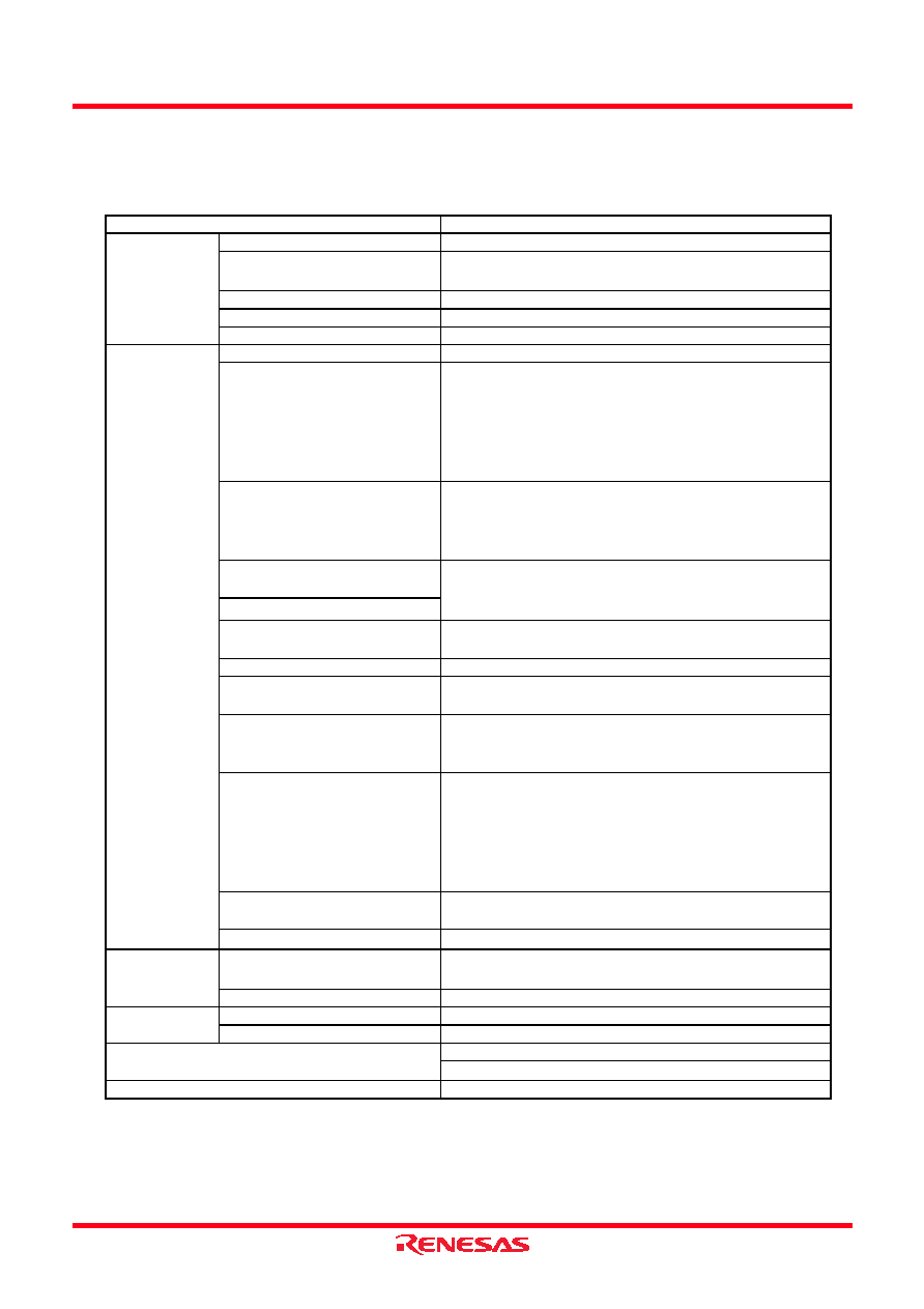
Table 1.1
R8C/20 Group Performance
Item
Performance
CPU
Number of Basic Instructions
89 instructions
Shortest Instruction Execution
Time
50ns (f(XIN)=20MHz, VCC=3.0 to 5.5V)
100ns (f(XIN)=10MHz, VCC=2.7 to 5.5V)
(1)
Operation Mode
Single-chip
Memory Space
1 Mbyte
Memory Capacity
See Table 1.3 Product Information
Peripheral
Function
Port
I/O port: 41 pins, Input port: 3 pins
Timer
Timer RA: 8 bits x 1 channel, Timer RB: 8 bits x 1
channel (Each timer equipped with 8-bit prescaler)
Timer RD: 16 bits x 2 channel
(Circuits of input capture and output compare)
Timer RE:
(With compare match function)
Serial Interface
1 channel
Clock synchronous, UART
1 channel
UART
Chip-select Clock Synchronous
Serial Interface (SSU)
1 channel
Chip-select clock synchronous serial interface (SSU),
I
2
C bus interface (IIC)
I
2
C Bus Interface (IIC)
(3)
LIN module
Hardware LIN: 1 channel
(Timer RA, UART)
A/D Converter
10-bit A/D converter: 1 circuit, 12 channels
Watchdog Timer
15 bits x 1 channel (with prescaler)
Reset start selectable
Interrupt
Internal: 11 factors, External: 5 factors, Software: 4
factors,
Priority level: 7 levels
Clock Generation Circuit
2 circuits
XIN clock generation circuit (Equipped with a built-in
feedback resistor)
On-chip oscillator (high speed, low speed)
High-speed on-chip oscillato r the frequency
adjustment function is usable.
Oscillation Stop Detection
Function
Stop detection of XIN clock oscillation
Voltage Detection Circuit
Included
(1)
Electric
Characteristics
Supply Voltage
VCC=3.0 to 5.5V (f(XIN)=20MHz)
VCC=2.7 to 5.5V (f(XIN)=10MHz)
(1)
Power Consumption
TBD
Flash Memory Program and Erase Supply Voltage VCC=2.7 to 5.5V
Program and Erase Endurance 100 times
Operating Ambient Temperature
-40 to 85
∞
C
-40 to 125
∞
C (Option
(2)
)
Package
48-pin plastic mold LQFP

R8C/20, R8C/21 Group
1. Overview
Rev.0.10
Mar 08, 2005
Page 3 of 21
REJ03B0120-0010
Under development
Preliminary specification
Specications in this manual are tentative and subject to change.
NOTES:
1. Because this product is under development, specifications may be changed.
2. When using options, be sure to inquire about the specification.
3. I
2
C bus is a registered trademark of Koninklijke Philips Electronics N.V.
Table 1.2
R8C/21 Group Performance
Item
Performance
CPU
Number of Basic Instructions
89 instructions
Shortest Instruction Execution
Time
50ns (f(XIN)=20MHz, VCC=3.0 to 5.5V)
100ns (f(XIN)=10MHz, VCC=2.7 to 5.5V)
(1)
Operation Mode
Single-chip
Memory Space
1 Mbyte
Memory Capacity
See Table 1.4 Product Information
Peripheral
Function
Port
I/O port: 41 pins, Input port: 3 pins
Timer
Timer RA: 8 bits x 1 channel, Timer RB: 8 bits x 1
channel (Each timer equipped with 8-bit prescaler)
Timer RD: 16 bits x 2 channel
(Circuits of input capture and output compare)
Timer RE:
(With compare match function)
Serial Interface
1 channel
Clock synchronous, UART
1 channel
UART
Chip-select Clock Synchronous
Serial Interface (SSU)
1 channel
Chip-select clock synchronous serial interface (SSU),
I
2
C bus interface (IIC)
I
2
C Bus Interface (IIC)
(3)
LIN module
Hardware LIN: 1 channel
(Timer RA, UART)
A/D Converter
10-bit A/D converter: 1 circuit, 12 channels
Watchdog Timer
15 bits x 1 channel (with prescaler)
Reset start selectable
Interrupt
Internal: 11 factors, External: 5 factors, Software: 4
factors,
Priority level: 7 levels
Clock Generation Circuit
2 circuits
XIN clock generation circuit (Equipped with a built-in
feedback resistor)
On-chip oscillator (high speed, low speed)
High-speed on-chip oscillato r the frequency
adjustment function is usable.
Oscillation Stop Detection
Function
Stop detection of XIN clock oscillation
Voltage Detection Circuit
Included
(1)
Electric
Characteristics
Supply Voltage
VCC=3.0 to 5.5V (f(XIN)=20MHz)
VCC=2.7 to 5.5V (f(XIN)=10MHz)
(1)
Power Consumption
TBD
Flash Memory Program and Erase Supply Voltage VCC=2.7 to 5.5V
Program and Erase Endurance 10,000 times (Data area)
1,000 times (Program area)
Operating Ambient Temperature
-40 to 85
∞
C
-40 to 125
∞
C (Option
(2)
)
Package
48-pin plastic mold LQFP
R8C/20, R8C/21 Group
1. Overview
Rev.0.10
Mar 08, 2005
Page 4 of 21
REJ03B0120-0010
Under development
Preliminary specification
Specications in this manual are tentative and subject to change.
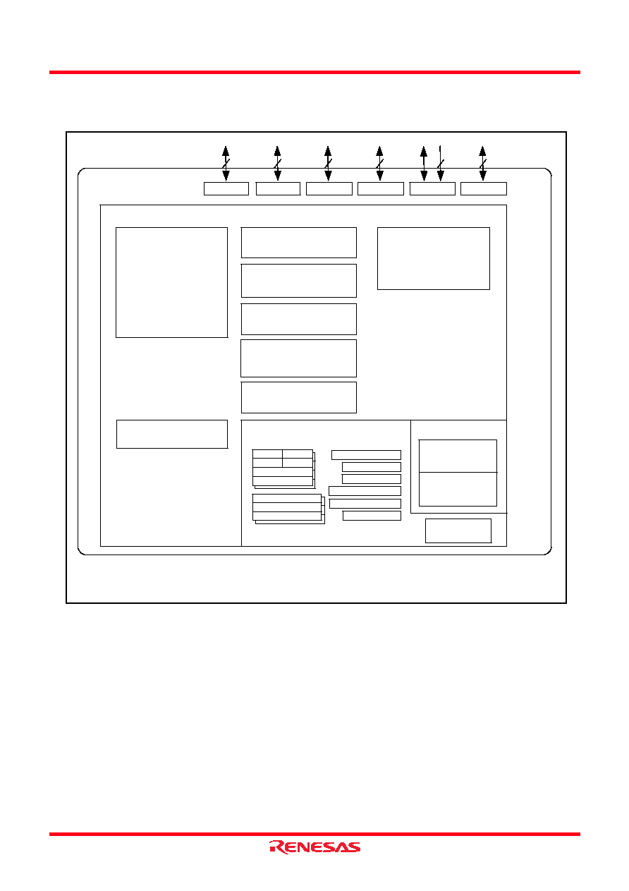
1.3
Block Diagram
Figure 1.1 shows a Block Diagram.
Figure 1.1
Block Diagram
R8C/Tiny Series CPU Core
Timer
Timer RA (8 bits)
Timer RB (8 bits)
Timer RD (16 bits
◊
2 channels)
Timer RE
A/D Converter
(10 bits
◊
12 channels)
System Clock Generation
XIN-XOUT
High-Speed On-Chip Oscillator
Low-Speed On-Chip Oscillator
UART or
Clock Synchronous Serial Interface
(8 bits
◊
1 channel)
Memory
Watchdog Timer
(15 bits)
ROM
(1)
RAM
(2)
Multiplier
R0H
R0L
R1H
R2
R3
R1L
A0
A1
FB
SB
USP
ISP
INTB
PC
FLG
I/O port
NOTES:
1. ROM size depends on MCU type.
2. RAM size depends on MCU type.
Chip-Select Clock Synchronous
Serial Interface or
I
2
C bus interface
(8 bits
◊
1 channel)
8
Port P1
6
Port P3
3
3
Port P4
8
Port P0
8
Port P2
8
Port P6
UART
(8 bits
◊
1 channel)
LIN Module
(1 channel)

R8C/20, R8C/21 Group
1. Overview
Rev.0.10
Mar 08, 2005
Page 5 of 21
REJ03B0120-0010
Under development
Preliminary specification
Specications in this manual are tentative and subject to change.
1.4
Product Information
Table 1.3 lists the Product Information of R8C/20 Group and Table 1.4 lists the Product Information of
R8C/21 Group.
(D): Under development
Figure 1.2
Part Number, Memory Size, and Package of R8C/20 Group
Table 1.3
Product Information of R8C/20 Group
As of Mar. 2005
Part Number
ROM Capacity
RAM Capacity
Package Type
Remarks
Program Area
R5F21206JFP (D)
32 Kbytes
2 Kbyte
PLQP0048KB-A
J Version
Flash Memory
Version
R5F21207JFP (D)
48 Kbytes
2.5 Kbytes
PLQP0048KB-A
R5F21206KFP (D)
32 Kbytes
2 Kbyte
PLQP0048KB-A
K Version
R5F21207KFP (D)
48 Kbytes
2.5 Kbytes
PLQP0048KB-A
Part Number
R 5 F 21 20 6 J FP
Package Type:
FP : PLQP0048KB-A
Shows Characteristics and Others
J : Operating Ambient Temperature -40 ∞C to 85 ∞C
K : Operating Ambient Temperature -40 ∞C to 125 ∞C
ROM Capacity
6 : 32KB
7 : 48KB
R8C/20 Group
R8C/Tiny Series
Memory Type
F : Flash Memory Version
Renesas MCU
Renesas Semiconductors

R8C/20, R8C/21 Group
1. Overview
Rev.0.10
Mar 08, 2005
Page 6 of 21
REJ03B0120-0010
Under development
Preliminary specification
Specications in this manual are tentative and subject to change.
(D): Under development
Figure 1.3
Part Number, Memory Size, and Package of R8C/21 Group
Table 1.4
Product Information of R8C/21 Group
As of Mar. 2005
Part Number
ROM Capacity
RAM Capacity
Package Type
Remarks
Program Area
Data Area
R5F21216JFP (D)
32 Kbytes
1 Kbyte X 2
2 Kbyte
PLQP0048KB-A J Version Flash
Memory
Version
R5F21217JFP (D)
48 Kbytes
1 Kbyte X 2
2.5 Kbytes
PLQP0048KB-A
R5F21216KFP (D)
32 Kbytes
1 Kbyte X 2
2 Kbyte
PLQP0048KB-A K Version
R5F21217KFP (D)
48 Kbytes
1 Kbyte X 2
2.5 Kbytes
PLQP0048KB-A
Part Number
R 5 F 21 21 6 J FP
Package Type:
FP : PLQP0048KB-A
Shows Characteristics and Others
J : Operating Ambient Temperature -40 ∞C to 85 ∞C
K : Operating Ambient Temperature -40 ∞C to 125 ∞C
ROM Capacity
6 : 32KB
7 : 48KB
R8C/21 Group
R8C/Tiny Series
Memory Type
F : Flash Memory Version
Renesas MCU
Renesas Semiconductors

R8C/20, R8C/21 Group
1. Overview
Rev.0.10
Mar 08, 2005
Page 7 of 21
REJ03B0120-0010
Under development
Preliminary specification
Specications in this manual are tentative and subject to change.
1.5
Pin Assignment
Figure 1.4 shows the Pin Assignment (top view).
Figure 1.4
Pin Assignment (top view)
48
P3_7/SSO
47
P0_0/AN7
46
P0_1/AN6
45
P0_2/AN5
44
P0_3/AN4
43
P6_1
42
P6_2
41
P6_0/TREO
40
P4_2/VREF
39
P0_4/AN3
38
P0_5/AN2
37
P0_6/AN1
13
14
15
16
17
18
19
20
21
22
23
24
P2_6/TRDIOC1
P2_5/TRDIOB1
P2_4/TRDIOA1
P2_3/TRDIOD0
P2_2/TRDIOC0
P2_1/TRDIOB0
P2_0/TRDIOA0/TCLK
P1_7/TRAIO/INT1
P1_6/CLK0
P1_5/RXD0 (/TRAIO/INT1)
P1_4/TXD0
P1_3/KI3/AN11
12
P
2
_
7
/TR
D
IOD
1
11
VCC
10
P
4
_6
/XIN
9
VS
S
8
(1
)
P
4_7/XOU
T
7
RE
S
E
T
6
P4
_
4
5
P4
_
3
4
MO
D
E
3
P3
_
4
/SC
S
(
/
SD
A
)
2
P3
_
3
/S
SI
1
P3
_
5
/SS
C
K(/
S
C
L
)
25
26
27
28
29
30
31
32
33
34
35
36
P
4
_5
/IN
T0
P
6
_6
/IN
T2 (
/
T
X
D
1
)
P
6
_7
/IN
T3 (
/
R
X
D1)
P
1
_2
/KI2/
A
N
1
0
P
1
_1
/KI1/
A
N
9
P
1
_0
/KI0/
A
N
8
P3
_
1
/
T
R
B
O
P3
_
0
/
T
R
A
O
P6
_
5
P6
_
4
P6
_
3
P0
_
7
/
A
N
0
Pin Assignment (top view)
Package: PLQP0048KB-A
R8C/20 Group
R8C/21 Group
NOTES:
1. P4_7 is a port for the input.

R8C/20, R8C/21 Group
1. Overview
Rev.0.10
Mar 08, 2005
Page 8 of 21
REJ03B0120-0010
Under development
Preliminary specification
Specications in this manual are tentative and subject to change.
1.6
Pin Description
Table 1.5 shows the Pin Description and Table 1.6 shows the Pin Name Information by Pin Number.
I: Input
O: Output
I/O: Input and output
Table 1.5
Pin Description
Function
Pin Name
I/O Type
Description
Power Supply Input
VCC
VSS
I
Apply 2.7 V to 5.5 V to the VCC pin. Apply 0 V to the
VSS pin.
Reset Input
RESET
I
Input "L" on this pin resets the MCU.
MODE
MODE
I
Connect this pin to VCC via a resistor.
XIN Clock Input
XIN
I
These pins are provided for the XIN clock generation
circuit I/O. Connect a ceramic resonator or a crystal
oscillator between the XIN and XOUT pins. To use an
externally derived clock, input it to the XIN pin and leave
the XOUT pin open.
XIN Clock Output
XOUT
O
INT Interrupt Input
INT0 to INT3
I
INT interrupt input pins.
Key Input Interrupt
KI0 to KI3
I
Key input interrupt input pins.
Timer RA
TRAIO
I/O
Timer RA I/O pin.
TRAO
O
Timer RA output pin.
Timer RB
TRBO
O
Timer RB output pin.
Timer RD
TRDIOA0, TRDIOA1,
TRDIOB0, TRDIOB1,
TRDIOC0, TRDIOC1,
TRDIOD0, TRDIOD1
I/O
Timer RD I/O ports.
TCLK
I
External clock input pin.
Timer RE
TREO
O
Divided clock output pin.
Serial Interface
CLK0
I/O
Transfer clock I/O pin.
RXD0, RXD1
I
Serial data input pins.
TXD0, TXD1
O
Serial data output pins.
SSU
SSI
I/O
Data I/O pin.
SCS
I/O
Chip-select signal I/O pin.
SSCK
I/O
Clock I/O pin.
SSO
I/O
Data I/O pin.
I
2
C Bus Interface (IIC)
SCL
I/O
Clock I/O pin.
SDA
I/O
Data I/O pin.
Reference Voltage Input VREF
I
Reference voltage input pin for A/D converter.
A/D Converter
AN0 to AN11
I
Analog input pins for A/D converter.
I/O Port
P0_0 to P0_7,
P1_0 to P1_7,
P2_0 to P2_7,
P3_0, P3_1,
P3_3 to P3_5, P3_7,
P4_3 to P4_5,
P6_0 to P6_7
I/O
These are CMOS I/O ports. Each port contains an input/
output select direction register, allowing each pin in that
port to be directed for input or output individually.
Any port set to input can select whether to use a pull-up
resistor or not by program.
Input Port
P4_2, P4_6, P4_7
I
Ports for input only.
R8C/20, R8C/21 Group
1. Overview
Rev.0.10
Mar 08, 2005
Page 9 of 21
REJ03B0120-0010
Under development
Preliminary specification
Specications in this manual are tentative and subject to change.
Table 1.6
Pin Name Information by Pin Number
Pin
Number
Control
Pin
Port
I/O Pin of Peripheral Function
Interrupt
Timer
Serial
Interface
Clock
Synchronous
Serial Interface
with Chip Select
I
2
C Bus
Interface
A/D
Converter
1
P3_5
SSCK
(SCL)
2
P3_3
SSI
3
P3_4
SCS
(SDA)
4
MODE
5
P4_3
6
P4_4
7
RESET
8
XOUT
P4_7
9
VSS
10
XIN
P4_6
11
VCC
12
P2_7
TRDIOD1
13
P2_6
TRDIOC1
14
P2_5
TRDIOB1
15
P2_4
TRDIOA1
16
P2_3
TRDIOD0
17
P2_2
TRDIOC0
18
P2_1
TRDIOB0
19
P2_0
TRDIOA0/TCLK
20
P1_7
INT1
TRAIO
21
P1_6
CLK0
22
P1_5
(INT1)
(TRAIO)
RXD0
23
P1_4
TXD0
24
P1_3
KI3
AN11
25
P4_5
INT0
26
P6_6
INT2
(TXD1)
27
P6_7
INT3
(RXD1)
28
P1_2
KI2
AN10
29
P1_1
KI1
AN9
30
P1_0
KI0
AN8
31
P3_1
TRBO
32
P3_0
TRAO
33
P6_5
34
P6_4
35
P6_3
36
P0_7
AN0
37
P0_6
AN1
38
P0_5
AN2
39
P0_4
AN3
40
VREF
P4_2
41
P6_0
TREO
42
P6_2
43
P6_1
44
P0_3
AN4
45
P0_2
AN5
46
P0_1
AN6
47
P0_0
AN7
48
P3_7
SSO

R8C/20, R8C/21 Group
2. Central Processing Unit (CPU)
Rev.0.10
Mar 08, 2005
Page 10 of 21
REJ03B0120-0010
Under development
Preliminary specification
Specications in this manual are tentative and subject to change.
2.
Central Processing Unit (CPU)
Figure 2.1 shows the CPU Register. The CPU contains 13 registers. Of these, R0, R1, R2, R3, A0, A1 and
FB comprise a register bank. Two sets of register banks are provided.
Figure 2.1
CPU Register
R2
b31
b15
b8b7
b0
Data Registers
(1)
Address Registers
(1)
R3
R0H (high-order of R0)
R2
R3
A0
A1
INTBH
b15
b19
b0
INTBL
FB
Frame Bass Registers
(1)
The 4-high order bits of INTB are INTBH and
the 16-low order bits of INTB are INTBL.
Interrupt Table Register
b19
b0
USP
Program Counter
ISP
SB
User Stack Pointer
Interrupt Stack Pointer
Static Base Register
PC
FLG
Flag Register
Carry Flag
Debug Flag
Zero Flag
Sign Flag
Register Bank Select Flag
Overflow Flag
Interrupt Enable Flag
Stack Pointer Select Flag
Reserved Area
Processor Interrupt Priority Level
Reserved Area
C
IPL
D
Z
S
B
O
I
U
b15
b0
b15
b0
b15
b0
b8
b7
NOTES:
1. A register bank comprises these registers. Two sets of register banks are provided.
R0L (low-order of R0)
R1H (high-order of R1) R1L (low-order of R1)

R8C/20, R8C/21 Group
2. Central Processing Unit (CPU)
Rev.0.10
Mar 08, 2005
Page 11 of 21
REJ03B0120-0010
Under development
Preliminary specification
Specications in this manual are tentative and subject to change.
2.1
Data Registers (R0, R1, R2 and R3)
R0 is a 16-bit register for transfer, arithmetic and logic operations. The same applies to R1 to R3.
R0 can be split into high-order bit (R0H) and low-order bit (R0L) to be used separately as 8-bit data
registers. The same applies to R1H and R1L as R0H and R0L. R2 can be combined with R0 to be used
as a 32-bit data register (R2R0). The same applies R3R1 as R2R0.
2.2
Address Registers (A0 and A1)
A0 is a 16-bit register for address register indirect addressing and address register relative addressing.
They also are used for transfer, arithmetic and logic operations. The same applies to A1 as A0.
A1 can be combined with A0 to be used a 32-bit address register (A1A0).
2.3
Frame Base Register (FB)
FB is a 16-bit register for FB relative addressing.
2.4
Interrupt Table Register (INTB)
INTB, a 20-bit register, indicates the start address of an interrupt vector table.
2.5
Program Counter (PC)
PC, 20 bits wide, indicates the address of an instruction to be executed.
2.6
User Stack Pointer (USP) and Interrupt Stack Pointer (ISP)
The stack pointer (SP), USP and ISP, are 16 bits wide each.
The U flag of FLG is used to switch between USP and ISP.
2.7
Static Base Register (SB)
SB is a 16-bit register for SB relative addressing.
2.8
Flag Register (FLG)
FLG is a 11-bit register indicating the CPU status.
2.8.1
Carry Flag (C Flag)
The C flag retains a carry, borrow, or shift-out bit that has occurred in the arithmetic and logic unit.
2.8.2
Debug Flag (D Flag)
The D flag is for debug only. Set to "0".
2.8.3
Zero Flag (Z Flag)
The Z flag is set to "1" when an arithmetic operation resulted in 0; otherwise, "0".
2.8.4
Sign Flag (S Flag)
The S flag is set to "1" when an arithmetic operation resulted in a negative value; otherwise, "0".
2.8.5
Register Bank Select Flag (B Flag)
The register bank 0 is selected when the B flag is "0". The register bank 1 is selected when this flag
is set to "1".
2.8.6
Overflow Flag (O Flag)
The O flag is set to "1" when the operation resulted in an overflow; otherwise, "0".

R8C/20, R8C/21 Group
2. Central Processing Unit (CPU)
Rev.0.10
Mar 08, 2005
Page 12 of 21
REJ03B0120-0010
Under development
Preliminary specification
Specications in this manual are tentative and subject to change.
2.8.7
Interrupt Enable Flag (I Flag)
The I flag enables a maskable interrupt.
An interrupt is disabled when the I flag is set to "0", and are enabled when the I flag is set to "1". The
I flag is set to "0" when an interrupt request is acknowledged.
2.8.8
Stack Pointer Select Flag (U Flag)
ISP is selected when the U flag is set to "0"; USP is selected when the U flag is set to "1".
The U flag is set to "0" when a hardware interrupt request is acknowledged or the INT instruction of
software interrupt numbers. 0 to 31 is executed.
2.8.9
Processor Interrupt Priority Level (IPL)
IPL, 3 bits wide, assigns processor interrupt priority levels from level 0 to level 7.
If a requested interrupt has greater priority than IPL, the interrupt is enabled.
2.8.10
Reserved Area
When write to this bit, set "0". When read, its content is indeterminate.

R8C/20, R8C/21 Group
3. Memory
Rev.0.10
Mar 08, 2005
Page 13 of 21
REJ03B0120-0010
Under development
Preliminary specification
Specications in this manual are tentative and subject to change.
3.
Memory
3.1
R8C/20 Group
Figure 3.1 is a Memory Map of the R8C/20 Group. The R8C/20 group provides 1-Mbyte address space
from address 00000h to FFFFFh.
The internal ROM is allocated lower addresses beginning with address 0FFFFh. For example, a 48-
Kbyte internal ROM is allocated addresses 04000h to 0FFFFh.
The fixed interrupt vector table is allocated addresses 0FFDCh to 0FFFFh. They store the starting
address of each interrupt routine here.
The internal RAM is allocated higher addresses direction beginning with address 00400h. For example,
a 2.5-Kbyte internal RAM is allocated addresses 00400h to 00DFFh. The internal RAM is used not only
for storing data but for calling subroutines and stacks when interrupt request is acknowledged.
Special function registers (SFR) are allocated addresses 00000h to 002FFh. The peripheral function
control registers are allocated them. Of the SFR, any space which has no functions allocated is
reserved for future use and cannot be accessed by users.
Figure 3.1
Memory Map of R8C/20 Group
Undefined Instruction
Overflow
BRK Instruction
Address Match
Single Step
Watchdog Timer∑Oscillation Stop Detection∑Voltage Detection
(Reserved)
(Reserved)
Reset
Part Number
Internal ROM
Internal RAM
Size
Address 0YYYYh
R5F21207JFP, R5F21207KFP
R5F21206JFP, R5F21206KFP
48 Kbytes
32 Kbytes
04000h
08000h
2.5 Kbytes
2 Kbytes
00DFFh
00BFFh
FFFFFh
0FFFFh
0YYYYh
0XXXXh
00400h
002FFh
00000h
Internal ROM
Expanding Area
Internal RAM
SFR
(See Chapter 4 for details.)
0FFFFh
0FFDCh
Size
Address 0XXXXh
02400h
Reserved Area
01300h
02000h

R8C/20, R8C/21 Group
3. Memory
Rev.0.10
Mar 08, 2005
Page 14 of 21
REJ03B0120-0010
Under development
Preliminary specification
Specications in this manual are tentative and subject to change.
3.2
R8C/21 Group
Figure 3.2 is a Memory Map of the R8C/213 Group. The R8C/21 group provides 1-Mbyte address space
from address 00000h to FFFFFh.
The internal ROM is allocated lower addresses direction beginning with address 0FFFFh. For example,
a 48-Kbyte internal ROM is allocated addresses 04000h to 0FFFFh.
The fixed interrupt vector table is allocated addresses 0FFDCh to 0FFFFh. They store the starting
address of each interrupt routine here.
The internal ROM (data area) is allocated addresses 02400h to 02BFFh.
The internal RAM is allocated higher addresses direction beginning with address 00400h. For example,
a 2.5-Kbyte internal RAM is allocated addresses 00400h to 00DFFh. The internal RAM calling
subroutines and stacks when interrupt request is acknowledged.
Special function registers (SFR) are allocated addresses 00000h to 002FFh. The peripheral function
control registers are allocated them. Of the SFR, any space which has no functions allocated is
reserved for future use and cannot be accessed by users.
Figure 3.2
Memory Map of R8C/21 Group
Undefined Instruction
Overflow
BRK Instruction
Address Match
Single Step
Watchdog Timer∑Oscillation Stop Detection∑Voltage Detection
(Reserved)
(Reserved)
Reset
Part Number
Internal ROM
Internal RAM
Size
Address 0YYYYh
R5F21217JFP, R5F21217KFP
R5F21216JFP, R5F21216KFP
48 Kbytes
32 Kbytes
04000h
08000h
2.5 Kbytes
2 Kbytes
00DFFh
00BFFh
FFFFFh
0FFFFh
0YYYYh
0XXXXh
00400h
002FFh
00000h
Internal ROM
(Program Area)
Expanding Area
Internal RAM
SFR
(See Chapter 4 for details.)
0FFFFh
0FFDCh
Size
Address 0XXXXh
02BFFh
02400h
Internal ROM
(Data Area)
(1)
NOTES:
1. This area is block A (1 Kbyte) and B (1 Kbyte) of the data flash ROM.
Reserved Area
01300h
02000h

R8C/20, R8C/21 Group
4. Special Function Register (SFR)
Rev.0.10
Mar 08, 2005
Page 15 of 21
REJ03B0120-0010
Under development
Preliminary specification
Specications in this manual are tentative and subject to change.
4.
Special Function Register (SFR)
SFR (Special Function Register) is the control register of peripheral functions.
Table 4.1 to Table 4.6 list the SFR Information.
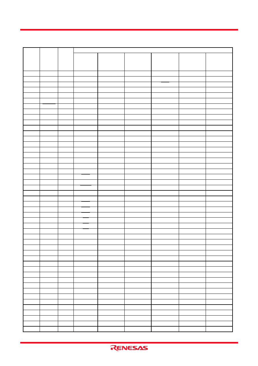
Table 4.1
SFR Information (1)
(1)
X: Undefined
NOTES:
1. Blank columns are reserved space. No access is allowed.
2. Software reset, the watchdog timer reset or the voltage monitor 2 reset does not affect this register.
3. Owing to Hardware Reset.
4. Owing to Power-on Reset or Voltage Monitor 1 Reset.
5. Software reset, the watchdog reset or the voltage monitor 2 reset does not affect the b2 and b3.
Address
Register
Symbol
After reset
0000h
0001h
0002h
0003h
0004h
Processor Mode Register 0
PM0
00h
0005h
Processor Mode Register 1
PM1
00h
0006h
System Clock Control Register 0
CM0
01101000b
0007h
System Clock Control Register 1
CM1
00100000b
0008h
0009h
000Ah
Protect Register
PRCR
00XXX000b
000Bh
000Ch
Oscillation Stop Detection Register
OCD
00000100b
000Dh
Watchdog Timer Reset Register
WDTR
XXh
000Eh
Watchdog Timer Start Register
WDTS
XXh
000Fh
Watchdog Timer Control Register
WDC
000XXXXXb
0010h
Address Match Interrupt Register 0
RMAD0
00h
0011h
00h
0012h
X0h
0013h
Address Match Interrupt Enable Register
AIER
XXXXXX00b
0014h
Address Match Interrupt Register 1
RMAD1
00h
0015h
00h
0016h
X0h
0017h
0018h
0019h
001Ah
001Bh
001Ch
Count Source Protect Mode Register
CSPR
00h
001Dh
001Eh
001Fh
0020h
0021h
0022h
0023h
High-Speed On-Chip Oscillator Control Register 0
FRA0
00h
0024h
High-Speed On-Chip Oscillator Control Register 1
FRA1
TBD
0025h
High-Speed On-Chip Oscillator Control Register 2
FRA2
00h
0026h
0030h
0031h
Voltage Detection Register 1
(2)
VCA1
00001000b
0032h
Voltage Detection Register 2
(2)
VCA2
00h
(3)
01000000b
(4)
0033h
0034h
0035h
0036h
Voltage Monitor 1 Circuit Control Register
(2)
VW1C
0000X000b
(3)
0100X001b
(4)
0037h
Voltage Monitor 2 Circuit Control Register
(5)
VW2C
00h
0038h
0039h
003Ah
003Bh
003Ch
003Dh
003Eh
003Fh
R8C/20, R8C/21 Group
4. Special Function Register (SFR)
Rev.0.10
Mar 08, 2005
Page 16 of 21
REJ03B0120-0010
Under development
Preliminary specification
Specications in this manual are tentative and subject to change.
Table 4.2
SFR Information (2)
(1)
X: Undefined
NOTES:
1. Blank columns are reserved space. No access is allowed.
2. The IICSEL bit in the RMR register switches functions.
Address
Register
Symbol
After reset
0040h
0041h
0042h
0043h
0044h
0045h
0046h
0047h
0048h
Timer RD0 Interrupt Control Register
TRD0IC
XXXXX000b
0049h
Timer RD1 Interrupt Control Register
TRD1IC
XXXXX000b
004Ah
Timer RE Interrupt Control Register
TREIC
XXXXX000b
004Bh
004Ch
004Dh
Key Input Interrupt Control Register
KUPIC
XXXXX000b
004Eh
A/D Conversion Interrupt Control Register
ADIC
XXXXX000b
004Fh
SSU Interrupt Control Register/IIC Interrupt Control Register
(2)
SSUAIC/IIC2AIC
XXXXX000b
0050h
0051h
UART0 Transmit Interrupt Control Register
S0TIC
XXXXX000b
0052h
UART0 Receive Interrupt Control Register
S0RIC
XXXXX000b
0053h
UART1 Transmit Interrupt Control Register
S1TIC
XXXXX000b
0054h
UART1 Receive Interrupt Control Register
S1RIC
XXXXX000b
0055h
INT2 Interrupt Control Register
INT2IC
XX00X000b
0056h
Timer RA Interrupt Control Register
TRAIC
XXXXX000b
0057h
0058h
Timer RB Interrupt Control Register
TRBIC
XXXXX000b
0059h
INT1 Interrupt Control Register
INT1IC
XX00X000b
005Ah
INT3 Interrupt Control Register
INT3IC
XX00X000b
005Bh
005Ch
005Dh
INT0 Interrupt Control Register
INT0IC
XX00X000b
005Eh
005Fh
0060h
0061h
0062h
0063h
0064h
0065h
0066h
0067h
0068h
0069h
006Ah
006Bh
006Ch
006Dh
006Eh
006Fh
0070h
0071h
0072h
0073h
0074h
0075h
0076h
0077h
0078h
0079h
007Ah
007Bh
007Ch
007Dh
007Eh
007Fh

R8C/20, R8C/21 Group
4. Special Function Register (SFR)
Rev.0.10
Mar 08, 2005
Page 17 of 21
REJ03B0120-0010
Under development
Preliminary specification
Specications in this manual are tentative and subject to change.
Table 4.3
SFR Information (3)
(1)
X: Undefined
NOTES:
1. Blank columns are reserved space. No access is allowed.
2. The IICSEL bit in the RMR register switches functions.
Address
Register
Symbol
After reset
0080h
0081h
0082h
0083h
0084h
0085h
0086h
0087h
0088h
0089h
008Ah
008Bh
008Ch
008Dh
008Eh
008Fh
0090h
0091h
0092h
0093h
0094h
0095h
0096h
0097h
0098h
0099h
009Ah
009Bh
009Ch
009Dh
009Eh
009Fh
00A0h
UART0 Transmit/Receive Mode Register
U0MR
00h
00A1h
UART0 Bit Rate Generator
U0BRG
XXh
00A2h
UART0 Transmit Buffer Register
U0TB
XXh
00A3h
XXh
00A4h
UART0 Transmit/Receive Control Register 0
U0C0
00001000b
00A5h
UART0 Transmit/Receive Control Register 1
U0C1
00000010b
00A6h
UART0 Receive Buffer Register
U0RB
XXh
00A7h
XXh
00A8h
UART1 Transmit/Receive Mode Register
U1MR
00h
00A9h
UART1 Bit Rate Register
U1BRG
XXh
00AAh
UART1 Transmit Buffer Register
U1TB
XXh
00ABh
XXh
00ACh
UART1 Transmit/Receive Control Register 0
U1C0
00001000b
00ADh
UART1 Transmit/Receive Control Register 1
U1C1
00000010b
00AEh
UART1 Receive Buffer Register
U1RB
XXh
00AFh
XXh
00B0h
00B1h
00B2h
00B3h
00B4h
00B5h
00B6h
00B7h
00B8h
SS Control Register H/IIC Bus Control Register 1
(2)
SSCRH/ICCR1
00h
00B9h
SS Control Register L/IIC Bus Control Register 2
(2)
SSCRL/ICCR2
01111101b
00BAh
SS Mode Register/IIC Bus Mode Register 1
(2)
SSMR/ICMR
00011000b
00BBh
SS Enable Register/IIC Interrupt Enable Register
(2)
SSER/ICIER
00h
00BCh
SS Status Register/IIC Bus Status Register
(2)
SSSR/ICSR
10000000b
00BDh
SS Mode Register 2/Slave Address Register
(2)
SSMR2/SAR
00h
00BEh
SS Transmit Data Register/IIC Bus Transmit Data Register
(2)
SSTDR/ICDRT
FFh
00BFh
SS Receive Data Register/IIC Bus Receive Data Register
(2)
SSRDR/ICDRR
FFh
R8C/20, R8C/21 Group
4. Special Function Register (SFR)
Rev.0.10
Mar 08, 2005
Page 18 of 21
REJ03B0120-0010
Under development
Preliminary specification
Specications in this manual are tentative and subject to change.
Table 4.4
SFR Information (4)
(1)
X: Undefined
NOTES:
1. Blank columns are reserved space. No access is allowed.
Address
Register
Symbol
After reset
00C0h
A/D Register
AD
XXh
00C1h
XXh
00C2h
00C3h
00C4h
00C5h
00C6h
00C7h
00C8h
00C9h
00CAh
00CBh
00CCh
00CDh
00CEh
00CFh
00D0h
00D1h
00D2h
00D3h
00D4h
A/D Control Register 2
ADCON2
00h
00D5h
00D6h
A/D Control Register 0
ADCON0
00000XXXb
00D7h
A/D Control Register 1
ADCON1
00h
00D8h
00D9h
00DAh
00DBh
00DCh
00DDh
00DEh
00DFh
00E0h
Port P0 Register
P0
XXh
00E1h
Port P1 Register
P1
XXh
00E2h
Port P0 Direction Register
PD0
00h
00E3h
Port P1 Direction Register
PD1
00h
00E4h
Port P2 Register
P2
XXh
00E5h
Port P3 Register
P3
XXh
00E6h
Port P2 Direction Register
PD2
00h
00E7h
Port P3 Direction Register
PD3
00h
00E8h
Port P4 Register
P4
XXh
00E9h
00EAh
Port P4 Direction Register
PD4
00h
00EBh
00ECh
Port P6 Register
P6
XXh
00EDh
00EEh
Port P6 Direction Register
PD6
00h
00EFh
00F0h
00F1h
00F2h
00F3h
00F4h
00F5h
00F6h
00F7h
00F8h
Port Mode Register
PMR
00h
00F9h
External Input Enable Register
INTEN
00h
00FAh
INT Input Filter Select Register
INTF
00h
00FBh
Key Input Enable Register
KIEN
00h
00FCh
Pull-Up Control Register 0
PUR0
00h
00FDh
Pull-Up Control Register 1
PUR1
XX00XX00b
00FEh
00FFh

R8C/20, R8C/21 Group
4. Special Function Register (SFR)
Rev.0.10
Mar 08, 2005
Page 19 of 21
REJ03B0120-0010
Under development
Preliminary specification
Specications in this manual are tentative and subject to change.
Table 4.5
SFR Information (5)
(1)
X: Undefined
NOTES:
1. Blank columns are reserved space. No access is allowed.
Address
Register
Symbol
After reset
0100h
Timer RA Control Register
TRACR
00h
0101h
Timer RA I/O Control Register
TRAIOC
00h
0102h
Timer RA Mode Register
TRAMR
00h
0103h
Timer RA Prescaler Register
TRAPRE
FFh
0104h
Timer RA Register
TRATR
FFh
0105h
0106h
LIN Control Register
LINCR
00h
0107h
LIN Status Register
LINST
00h
0108h
Timer RB Control Register
TRBCR
00h
0109h
Timer RB One-Shot Control Register
TRBOCR
00h
010Ah
Timer RB I/O Control Register
TRBIOC
00h
010Bh
Timer RB Mode Register
TRBMR
00h
010Ch
Timer RB Prescaler Register
TRBPRE
FFh
010Dh
Timer RB Secondary Register
TRBSC
FFh
010Eh
Timer RB Primary
TRBPR
FFh
010Fh
0110h
0111h
0112h
0113h
0114h
0115h
0116h
0117h
0118h
Timer RE Counter Data Register
TRESEC
00h
0119h
Timer RE Comparison Register
TREMIN
00h
011Ah
011Bh
011Ch
Timer RE Control Register 1
TRECR1
00h
011Dh
Timer RE Control Register 2
TRECR2
00h
011Eh
Timer RE Clock Source Select Register
TRECSR
00001000b
011Fh
0120h
0121h
0122h
0123h
0124h
0125h
0126h
0127h
0128h
0129h
012Ah
012Bh
012Ch
012Dh
012Eh
012Fh
0130h
0131h
0132h
0133h
0134h
0135h
0136h
0137h
Timer RD Start Register
TRDSTR
11111100b
0138h
Timer RD Mode Register
TRDMDR
00001110b
0139h
Timer RD PWM Mode Register
TRDPMR
10001000b
013Ah
Timer RD Function Control Register
TRDFCR
10000000b
013Bh
Timer RD Output Master Enable Register 1
TRDOER1
FFh
013Ch
Timer RD Output Master Enable Register 2
TRDOER2
01111111b
013Dh
Timer RD Output Control Register
TRDOCR
00h
013Eh
Timer RD Digital Filter Function Select Register 0
TRDDF0
00h
013Fh
Timer RD Digital Filter Function Select Register 1
TRDDF1
00h

R8C/20, R8C/21 Group
4. Special Function Register (SFR)
Rev.0.10
Mar 08, 2005
Page 20 of 21
REJ03B0120-0010
Under development
Preliminary specification
Specications in this manual are tentative and subject to change.
Table 4.6
SFR Information (6)
(1)
X: Undefined
NOTES:
1. Blank columns are reserved space. No access is allowed.
2. The OFS register cannot be changed by program. Use a flash programmer to write to it.
Address
Register
Symbol
After reset
0140h
Timer RD Control Register 0
TRDCR0
00h
0141h
Timer RD I/O Control Register A0
TRDIORA0
10001000b
0142h
Timer RD I/O Control Register C0
TRDIORC
10001000b
0143h
Timer RD Status Register 0
TRDSR0
11100000b
0144h
Timer RD Interrupt Enable Register 0
TRDIER0
11100000b
0145h
Timer RD PWM Mode Output Level Control Register 0
POCR0
11111000b
0146h
Timer RD Counter 0
TRDCNT0
00h
0147h
00h
0148h
Timer RD General Register A0
GRA0
FFh
0149h
FFh
014Ah
Timer RD General Register B0
GRB0
FFh
014Bh
FFh
014Ch
Timer RD General Register C0
GRC0
FFh
014Dh
FFh
014Eh
Timer RD General Register D0
GRD0
FFh
014Fh
FFh
0150h
Timer RD Control Register 1
TRDCR1
00h
0151h
Timer RD I/O Control Register A1
TRDIORA1
10001000b
0152h
Timer RD I/O Control Register C1
TRDIORC1
10001000b
0153h
Timer RD Status Register 1
TRDSR1
11000000b
0154h
Timer RD Interrupt Enable Register 1
TRDIER1
11100000b
0155h
Timer RD PWM Mode Output Level Control Register 1
POCR1
11111000b
0156h
Timer RD Counter 1
TRDCNT1
00h
0157h
00h
0158h
Timer RD General Register A1
GRA1
FFh
0159h
FFh
015Ah
Timer RD General Register B1
GRB1
FFh
015Bh
FFh
015Ch
Timer RD General Register C1
GRC1
FFh
015Dh
FFh
015Eh
Timer RD General Register D1
GRD1
FFh
015Fh
FFh
0160h
0161h
0162h
0163h
0164h
0165h
0166h
0167h
0168h
0169h
016Ah
016Bh
016Ch
016Dh
016Eh
016Fh
01B0h
01B1h
01B2h
01B3h
Flash Memory Control Register 4
FMR4
01000000b
01B4h
01B5h
Flash Memory Control Register 1
FMR1
01000101b
01B6h
01B7h
Flash Memory Control Register 0
FMR0
XX000001b
01B8h
01B9h
01BAh
01BBh
01BCh
01BDh
01BEh
01BFh
FFFFh
Option Function Select Register
OFS
(2)

R8C/20, R8C/21 Group
Appendix 1. Package Dimensions
Rev.0.10
Mar 08, 2005
Page 21 of 21
REJ03B0120-0010
Under development
Preliminary specification
Specications in this manual are tentative and subject to change.
Appendix 1. Package Dimensions
Terminal cross section
b
1
c
1
bp
c
2.
1.
DIMENSIONS "
*1" AND "*2"
DO NOT INCLUDE MOLD FLASH.
NOTE)
DIMENSION "
*3" DOES NOT
INCLUDE TRIM OFFSET.
Detail F
L
1
c
A
L
A
1
A
2
*3
F
48
37
36
25
24
13
12
1
*1
*
2
x
Index mark
y
Z
E
Z
D
b
p
e
H
E
H
D
D
E
Previous Code
JEITA Package Code
RENESAS Code
PLQP0048KB-A
48P6Q-A
MASS[Typ.]
0.2g
P-LQFP48-7x7-0.50
1.0
0.125
0.20
0.75
0.75
0.08
0.20
0.145
0.09
0.27
0.22
0.17
Max
Nom
Min
Dimension in Millimeters
Symbol
Reference
7.1
7.0
6.9
D
7.1
7.0
6.9
E
1.4
A
2
9.2
9.0
8.8
9.2
9.0
8.8
1.7
A
0.2
0.1
0
0.65
0.5
0.35
L
x
8∞
0
∞
c
0.5
e
0.10
y
H
D
H
E
A
1
b
p
b
1
c
1
Z
D
Z
E
L
1

Keep safety first in your circuit designs!
1. Renesas Technology Corp. puts the maximum effort into making semiconductor products better and more reliable, but there is always the possibility that trouble
may occur with them. Trouble with semiconductors may lead to personal injury, fire or property damage.
Remember to give due consideration to safety when making your circuit designs, with appropriate measures such as (i) placement of substitutive, auxiliary circuits,
(ii) use of nonflammable material or (iii) prevention against any malfunction or mishap.
Notes regarding these materials
1. These materials are intended as a reference to assist our customers in the selection of the Renesas Technology Corp. product best suited to the customer's
application; they do not convey any license under any intellectual property rights, or any other rights, belonging to Renesas Technology Corp. or a third party.
2. Renesas Technology Corp. assumes no responsibility for any damage, or infringement of any third-party's rights, originating in the use of any product data,
diagrams, charts, programs, algorithms, or circuit application examples contained in these materials.
3. All information contained in these materials, including product data, diagrams, charts, programs and algorithms represents information on products at the time of
publication of these materials, and are subject to change by Renesas Technology Corp. without notice due to product improvements or other reasons. It is
therefore recommended that customers contact Renesas Technology Corp. or an authorized Renesas Technology Corp. product distributor for the latest product
information before purchasing a product listed herein.
The information described here may contain technical inaccuracies or typographical errors.
Renesas Technology Corp. assumes no responsibility for any damage, liability, or other loss rising from these inaccuracies or errors.
Please also pay attention to information published by Renesas Technology Corp. by various means, including the Renesas Technology Corp. Semiconductor
home page (http://www.renesas.com).
4. When using any or all of the information contained in these materials, including product data, diagrams, charts, programs, and algorithms, please be sure to
evaluate all information as a total system before making a final decision on the applicability of the information and products. Renesas Technology Corp. assumes
no responsibility for any damage, liability or other loss resulting from the information contained herein.
5. Renesas Technology Corp. semiconductors are not designed or manufactured for use in a device or system that is used under circumstances in which human life
is potentially at stake. Please contact Renesas Technology Corp. or an authorized Renesas Technology Corp. product distributor when considering the use of a
product contained herein for any specific purposes, such as apparatus or systems for transportation, vehicular, medical, aerospace, nuclear, or undersea repeater
use.
6. The prior written approval of Renesas Technology Corp. is necessary to reprint or reproduce in whole or in part these materials.
7. If these products or technologies are subject to the Japanese export control restrictions, they must be exported under a license from the Japanese government and
cannot be imported into a country other than the approved destination.
Any diversion or reexport contrary to the export control laws and regulations of Japan and/or the country of destination is prohibited.
8. Please contact Renesas Technology Corp. for further details on these materials or the products contained therein.
Sales Strategic Planning Div. Nippon Bldg., 2-6-2, Ohte-machi, Chiyoda-ku, Tokyo 100-0004, Japan
http://www.renesas.com
Refer to "http://www.renesas.com/en/network" for the latest and detailed information.
Renesas Technology America, Inc.
450 Holger Way, San Jose, CA 95134-1368, U.S.A
Tel: <1> (408) 382-7500, Fax: <1> (408) 382-7501
Renesas Technology Europe Limited
Dukes Meadow, Millboard Road, Bourne End, Buckinghamshire, SL8 5FH, U.K.
Tel: <44> (1628) 585-100, Fax: <44> (1628) 585-900
Renesas Technology
Hong Kong Ltd.
7th Floor, North Tower, World Finance Centre, Harbour City, 1 Canton Road, Tsimshatsui, Kowloon, Hong Kong
Tel: <852> 2265-6688, Fax: <852> 2730-6071
Renesas Technology Taiwan Co.,
Ltd.
10th Floor, No.99, Fushing North Road, Taipei, Taiwan
Tel: <886> (2) 2715-2888, Fax: <886> (2) 2713-2999
Renesas Technology (Shanghai) Co.,
Ltd.
Unit2607 Ruijing Building, No.205 Maoming Road (S), Shanghai 200020, China
Tel: <86> (21) 6472-1001, Fax: <86> (21) 6415-2952
Renesas Technology Singapore Pte. Ltd.
1 Harbour Front Avenue, #06-10, Keppel Bay Tower, Singapore 098632
Tel: <65> 6213-0200, Fax: <65> 6278-8001
RENESAS SALES OFFICES
© 2005. Renesas Technology Corp., All rights reserved. Printed in Japan.
Colophon 2.0