1
Æ
DM1800-
434MN
Rating
Value
Units
All Input/Output Pins Except VIN
-0.3 to +3.3
V
Non-Operating Ambient Temperature Range
-50 to +100
o
C
Absolute Maximum Ratings
Preliminary
Electrical Characteristics
Characteristic
Sym
Notes
Minimum
Typical
Maximum
Units
Operating Frequency
f
O
433.72
434.12
MHz
Modulation Type
OOK
RF Encoded Data Transmission Rate
4.8
kb/s
Average Receiver Input Current, No External Power Supply Load
I
R
4
mA
Receiver Input Signal for 10
-3
BER, 25 ∞C
-103
dBm
Peak Transmitter Input Current, No External Power Supply Load
I
TP
13.5
mA
Peak Transmitter Output Power
P
O
1
mW
Analog Input Measurement Range (10-bit ADC)
0
VOUT
V
Source Impedance to Analog Input
10
K
Digital In Logic High
2.4
V
Digital In Logic Low
.45
V
Digital Out Logic High, No Load
2.4
V
Digital In Logic Low, No Load
0.3
V
Digital Output Source Current, 1K load
1.1
mA
Digital Output Sink Current, 1K load
1.2
mA
Serial Port Data Rate
9.6
kb/s
Power Supply Input Voltage Range, -40 to +85
o
C
VIN
3.1
14
V
Power Supply Input Voltage Range, 0 to +85
o
C
VIN
2.6
14
V
Regulated Power Supply Output Voltage, VIN 3.1 to 14 V
VOUT
3.0
Vdc
Regulated Power Supply Voltage Ripple
10
mV
P-P
The DM1800-434MN is the 433.92 MHz field node module in the DM1800 family of RF transceiv-
ers. The DM1800 family is designed for adding embedded wireless connectivity to a wide range of
monitoring and control systems. The DM1800-434MN is equipped with a serial I/O port to interface
to a host microcontroller. The module also includes an analog input, a logic input, and a logic out-
put for monitoring and control. Radio communications range in an "open field" environment is typi-
cally 200 meters/hop. The DM1800-434MN combines RFM's very low current ASH radio tech-
nology with low power microcontroller technology to achieve long battery life. This module is com-
patible with RFM's miniMESH
TM
network protocol, which provides add-on "plug- and-play" multicast
mesh network routing. The DM1800-434MN is designed for operation under ETSI I-ETS 300 220
regulations.
∑
Field Node with Host Serial Interface
∑
Compatible with RFM miniMESH
TM
Network Protocol
∑
3 V, Very Low Current Operation
∑
Ready-to-Use OEM Module
433.92 MHz
Transceiver
Module
2
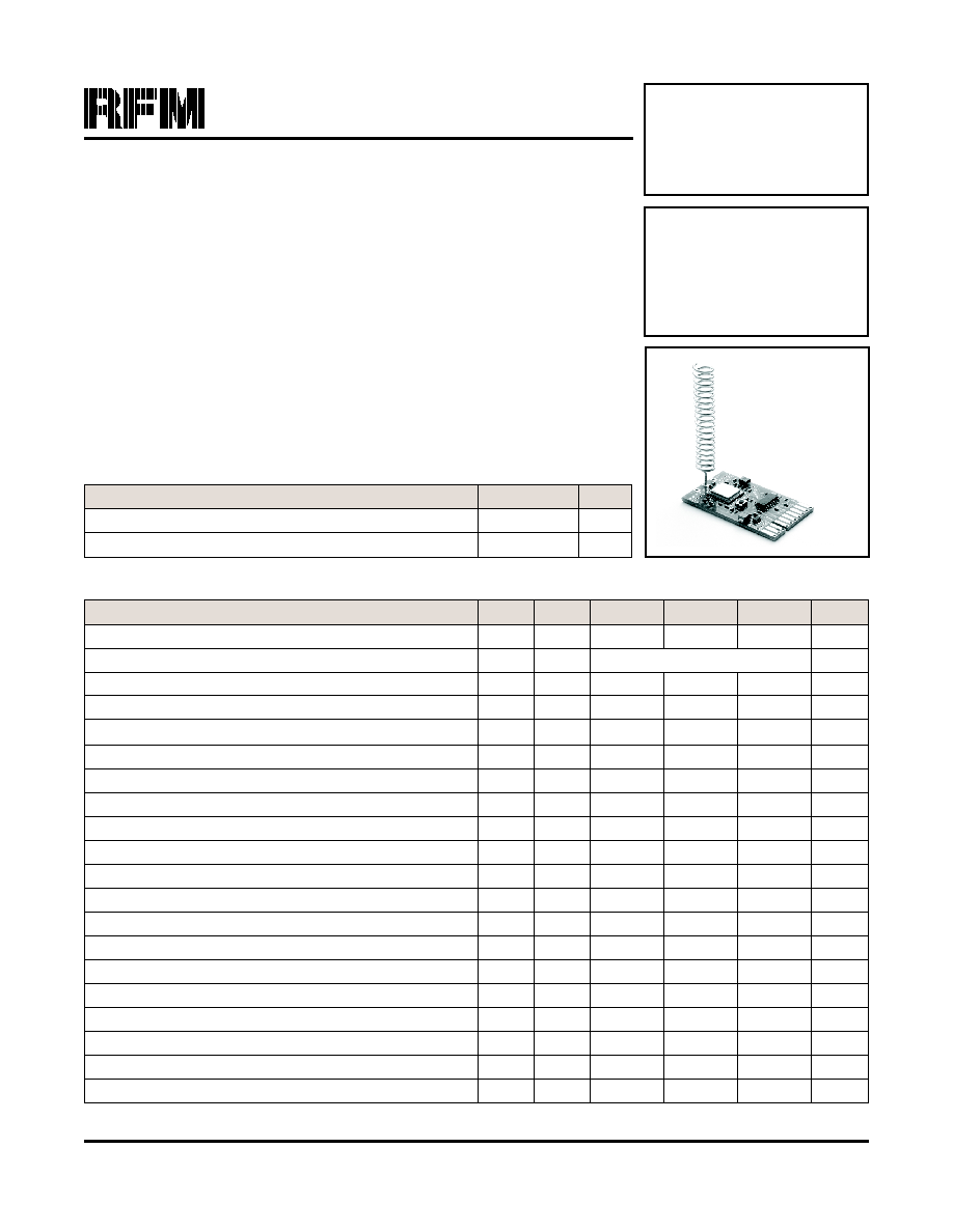
Theory of Operation
The major components of the DM1800-
433.92MN include an RFM TR3000 ASH
transceiver and a Microchip PIC16F688
microcontroller. The TR3000 operates on a
frequency of 433.92 MHz, at a nominal out-
put power of 1 mW.
The 16F688 provides a 9.6 kb/s serial inter-
face for communication with a host micro-
controller. A companion interface board is
also available with USB bridge circuitry to in-
terface the DM1800 to a host PC. Three of
the 16F688 I/O pins are configured for exter-
nal monitoring or control. Digital In is config-
ured as a logic input with a weak pull-up for
sensing a contact closure to a DM1800
ground pad. Digital Out is configured a logic
output. Analog In is configured as a 10-bit
analog-to-digital input. The DM1800 includes
two LEDs that indicate the module's operat-
ing mode. The LEDs can be disabled for low
current operation.
The DM1800-434MN is compatible with
RFM's miniMESH
TM
network protocol, which
provides add-on "plug-and-play" multicast
mesh network routing to improve communi-
cation range and robustness.
T X M O D
R X D A T A
C N T R L 1
C N T R L 0
P I C
1 6 F 6 8 8
µ P
D M 1 8 0 0 - 4 3 4 M N B l o c k D i a g r a m
L E D 1
L E D 2
A S H
T r a n s c e i v e r
G N D
S E R I A L T X
S E R I A L R X
D I G I T A L O U T
A N A L O G I N
D I G I T A L I N
B I N D
G N D
V O U T
V I N
3 V
R e g
G N D
G N D
J 1 - 1
J 1 - 2
J 1 - 3
J 1 - 4
J 1 - 5
J 1 - 6
J 1 - 7
J 1 - 8
J 1 - 9
J 1 - 1 0
J 2 - 2
J 2 - 1
J 2 - 3
Figure 1

Pin
Name
Description
J1-1
GND
This pad is a signal and power supply ground.
J1-2
VIN
This is the power supply input pad. The allowed input voltage range is 2.6 to 14 V.
J1-3
VOUT
VOUT tracks 50 to 100 mV below VIN when VIN is in the range of 2.6 to 3.1 V. When VIN is in the range of 3.1
to 14 V, VOUT is regulated at 3.0 Vdc. Up to 10 mA can be supplied from this pad for powering external circuits
such as thermistor-resistor networks. External circuitry must not impress more than 10 mV
p-p
ripple on the regu-
lated output voltage.
J1-4
BIND
This pad is connected to a logic input on the microcontroller, and is configured with a weak pull-up. When this pin
is momentarily grounded (to J1-1 or J1-10, the module is placed into the bind mode, allowing this module to be
associated with other modules to form a network.
J1-5
DIGITAL IN
This pad is connected to a logic input on the microcontroller, and is configured with a weak pull-up, allowing
both logic signals and contact closures referenced to J-1 or J-10 to be read. The value of this input is sent over
the RF channel as a response to an RF command. The input voltage range on this pad is 0 to VOUT. Applying
a voltage outside of this range may damage the module.
J1-6
ANALOG IN
This pad in the input to the microcontroller's 10-bit analog-to-digital (ADC) converter. The ADC input range is 0
to VOUT, referenced to J1-1 or J1-10. The input voltage range on this pad is 0 to VOUT. Applying a voltage
outside of this range may damage the module. The ADC reading is sent over the RF channel as a response to
an RF command.
J1-7
DIGITAL OUT
This pad is connected to a logic output on the microcontroller through a 1 kilohm resistor, which provides
short-circuit protection. The value of this output is set or read over the RF channel as a response to an RF com-
mand.
J1-8
SERIAL RX
This pad is connected to the module's serial data input (USART). Data to this pin is received at 9.6 kb/s, using
8 data bits, no parity, and one stop bit. The input voltage range on this pad is 0 to VOUT. Applying a voltage
outside of this range may damage the module.
J1-9
SERIAL TX
This pad is connected to the module's serial data output (USART) through a 1 kilohm resistor, which provides
short-circuit protection. Data from this pad is sent at 9.6 kb/s, using 8 data bits, no parity, and one stop bit.
J1-10
GND
This pad is a signal and power supply ground.
J2-1
GND
This pad is a ground for the antenna port.
J2-2
ANT
This pad is the antenna port.
J2-3
GND
This pad is a ground for the antenna port.
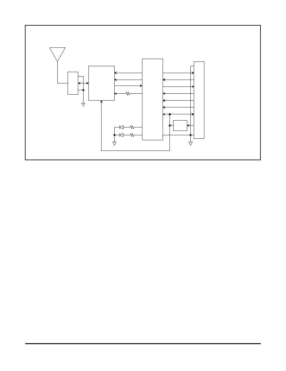
3
DM1800-434MN I/O Pad Descriptions
4
G N D
V I N
V O U T
B I N D
D I G I T A L I N
A N A L O G I N
D I G I T A L O U T
S E R I A L R X
G N D
S E R I A L T X
R F I O
G N D
G N D
D M 1 8 0 0 - 4 3 4 M N I / O P a d L a b e l s
Figure 2
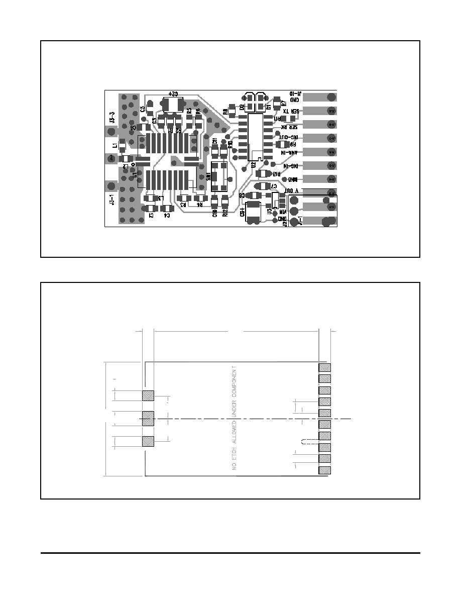
. 0 9 5
. 0 8 0
1 . 5 3 5
D M 1 8 0 0 - 4 3 4 M N S M T M o u n t i n g P a t t e r n
1.
000
.1
3
0
.0
9
0
.0
9
0
.2
0
0
.2
0
0
.0
5
0
.
0
70
T
Y
P
.
1
00
T
Y
P
D i m e n s i o n s i n i n c h e s . P C B p l u s c o m p o n e n t h e i g h t i s . 1 7 0 m a x ;
P C B p l u s a n t e n n a h e i g h t i s 2 . 1 5 m a x
Figure 3
Note: Specifications subject to change without notice.
file: dm1800nj.vp, 2005.11.11 rev