 | –≠–ª–µ–∫—Ç—Ä–æ–Ω–Ω—ã–π –∫–æ–º–ø–æ–Ω–µ–Ω—Ç: IM1800 | –°–∫–∞—á–∞—Ç—å:  PDF PDF  ZIP ZIP |
1
Æ
IM1800
The IM1800 is designed as an application interface module for the DM1800 series transceivers.
The IM1800 can be powered from either its USB interface or from an external DC power input. The
IM1800 USB interface is supported by a host computer virtual serial port driver. In addition, the
IM1800 provides terminal block connections for an analog input, a logic input and a logic output.
Direct connections to the DM1800 transceiver module USART are also provided on the IM1800
terminal block.
Rating
Value
Units
VIN
-0.3 to +16.0
V
All Other Input/Output Connections
-0.3 to +4.0
V
Non-Operating Ambient Temperature Range
-50 to +100
o
C
Absolute Maximum Ratings
∑
Application Interface Module for the DM1800 Transceiver Modules
∑
USB Host Computer Interface with Virtual Serial Port Driver
∑
Choice of USB or External DC Power Sources
∑
Supports Analog and Logic Inputs and a Logic Output
Electrical Characteristics
Characteristic
Sym
Notes
Minimum
Typical
Maximum
Units
Digital Output Source Current
0.5
mA
Digital Output Sink Current
1
mA
Virtual Serial Port Data Rate
9.6
kb/s
Power Supply Input Voltage Range, -40 to +85
o
C
VIN
3.1
14
V
Power Supply Input Voltage Range, 0 to +85
o
C
VIN
2.6
14
V
Regulated Power Supply Output Voltage, VIN 3.1 to 14 V
VOUT
3.0
Vdc
Current Available for External Circuitry
10
mA
Transceiver
Interface
Module
Preliminary

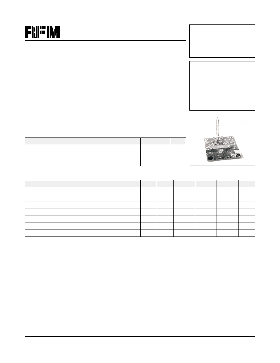
IM1800 Applications
The IM1800 is a companion interface board for the
DM1800 series transceiver modules. It has two uses:
First, the IM1800 can be used as a general purpose in-
terface for DM1800 series transceiver modules. For this
application, the IM1800 provides a captured screw I/O
terminal block, a virtual serial port USB interface, and a
choice of USB, coaxial plug or terminal block for the DC
power supply input. For DM1800 base stations and field
nodes, the IM1800 supports serial communications
through the virtual serial port USB interface, or by direct
connection to the USART on the DM1800 module.
Second, the IM1800 can be used as a development
platform for applications where a DM1800 series trans-
ceiver will be installed a customer's board. In addition to
the features listed above, the IM1800 provides a con-
nector strip for jumpering a flat cable to a customer's
board (or for a logic analyzer/oscilloscope connection),
and a "bread board" area for building and testing inter-
face circuits.
Power Supply Options
The IM1800 will accepts an external DC power supply
voltage in the range of 2.6 to 14 V (3.1 to 14 V for ex-
tended temperature operation). This voltage is routed to
the 3 Vdc regulator on the DM1800 transceiver (see
description of J2-3 on Page 3 for VOUT characteristics).
The external power supply voltage can be connected to
VIN on terminal block J2 or to the coaxial power con-
nector J6. The IM1800 can also be powered from the
USB connector J1. When the IM1800 is powered from
the USB connector, no connection should be made to
the VIN terminal on terminal block J2 or to the coaxial
power connector J6.
Serial Port Options
The IM1800 provides direct connections to the DM1800
transceiver module USART on terminal block J2. Note
that the DM1800 USART I/O is 3 V CMOS logic. Alter-
nately, the serial port on a DM1800 can be interfaced
through the serial port-USB bridge IC on the IM1800.
Only one interface should be used at a time; the other
serial interface should remain unconnected. The
IM1800 virtual serial port USB interface is based on the
Silicon Labs CP2101 IC. The CP2101 drivers can be
downloaded from www.silabs.com. After the correct
driver has been installed on a host PC, the USB inter-
face will appear as a serial port.
Bread Boarding Area
Referring to Figure 1, the IM1800 bread boarding area
is supplied with ground connections on eyelet Row 10
(vertical row of eyelets on right side), VOUT on eyelet
Row 3, and VIN on eyelet Row 2. VOUT and the I/O
signals from the DM1800 are also provided in two loca-
tions on Row 1. Refer to the table on Pages 3 and 4 for
details. Note that the DM1800 can provide up to 10 mA
for supplying external circuitry. Additional power can be
provided by adding a 3 V regulator in the bread board-
ing area and running it from VIN. Take caution not to
operate circuitry from VIN that directly interfaces the
DM1800 I/O signals to avoid damaging the DM1800
and/or IM1800. Note that any components placed on
the bread boarding area directly under where the
DM1800 module plugs in must be no taller than 0.1
inch.
I/O and Power Supply Precautions
Note that all analog and digital input signals must be
within the range of 0 to VOUT. Applying a signal outside
of this range may damage the DM1800 and/or IM1800.
External DC power supplies must be in the range of 2.6
to 14 V. Suitable external power supplies include batter-
ies and transformer isolated, regulated DC power sup-
plies. Be cautious when using unregulated "wall
transformer" DC supplies. The output voltage of these
unregulated supplies can be much higher than the
nameplate value when powering low current loads.
Note: the IM1800 is equipped with a programming con-
nector compatible with a Microchip MPLAB
Æ
ICD 2. Ex-
cept in special circumstances, however, all DM1800
transceiver modules are shipped pre-programmed. Re-
programming a pre-programmed DM1800 transceiver
module will void the warranty and any regulatory certifi-
cations of the module.
2
Pin
Name
Description
J1-1
VBUS
This is the USB VBUS. The IM1800 and its DM1800 transceiver module can be powered from this supply.
J1-2
D-
This is the USB D- signal.
J1-3
D+
This is the USB D+ signal.
J1-4
GND
This is a signal and power supply ground for the USB connector.
J1-5
GND
This is a signal and power supply ground for the USB connector.
J1-6
GND
This is a signal and power supply ground for the USB connector.
J2-1
J3-1
J4-1
GND
This is a signal and power supply ground.
J2-2
J3-2
J4-2
VIN
This is the power supply positive input. The allowed input voltage range is 2.6 to 14 V.
J2-3
J3-3
J4-3
R1-7
R1-28
VOUT
VOUT tracks 50 to 100 mV below VIN when VIN is in the range of 2.6 to 3.1 V. When VIN is in the range of 3.1
to 14 V, VOUT is regulated at 3.0 Vdc. Up to 10 mA can be supplied for powering external circuits such as
thermistor-resistor networks. External circuitry must not impress more than 10 mV
p-p
ripple on the regulated
output voltage.
J2-4
J3-4
J4-4
R1-6
R1-27
BIND
This is connected to a logic input on the microcontroller, and is configured with a weak pull-up. When this pin is
momentarily grounded (to J1-1 or J1-10, the module is placed into the bind mode, allowing this module to be
associated with other modules to form a network.
J2-5
J3-5
J4-5
R1-5
R1-26
DIGITAL
IN
This is connected to a logic input on the microcontroller, and is configured with a weak pull-up, allowing both
logic signals and contact closures referenced to J-1 or J-10 to be read. The value of this input is sent over the
RF channel as a response to an RF command. The input voltage range on this pad is 0 to VOUT. Applying a
voltage outside of this range may damage the module.
J2-6
J3-6
J4-6
R1-4
R1-25
ANALOG
IN
This is connected to the input to the microcontroller's 10-bit analog-to-digital (ADC) converter. The ADC input
range is 0 to VOUT, and the input voltage range on this pad is 0 to VOUT. Applying a voltage outside of this
range may damage the module. The reading is sent over the RF channel as a response to an RF command.
J2-7
J3-7
J4-7
R1-3
R1-24
DIGITAL
OUT
This is connected to a logic output on the microcontroller through a 1 kilohm resistor, which provides short-
circuit protection. The value of this output is set or read over the RF channel as a response to an RF command.
J2-8
J3-8
J4-8
R1-2
R1-23
SERIAL
RX
This is connected to the module's serial data input (USART). Data to this input is received at 9.6 kb/s, using 8
data bits, no parity, and one stop bit. The input voltage range on this pad is 0 to VOUT. Applying a voltage out-
side of this range may damage the module.
J2-9
J3-9
J4-9
R1-1
R1-22
SERIAL
TX
This is the connected to the module's serial data output (USART) through a 1 kilohm resistor, which provides
short-circuit protection. Data from this output is sent at 9.6 kb/s, using 8 data bits, no parity, and one stop bit.
J2-10
J3-10
J4-10
GND
This is a signal and power supply ground.
J5-1
Vpp/~MCLR
This is the programming connector microcontroller reset and programming voltage pulse input.
3
Connector and Terminal Block Descriptions

Pin
Name
Description
J5-2
VDD
This is the programming connector positive voltage input.
J5-3
GND
This is the programming connector ground.
J5-4
PGD
This is the programming connector data input.
J5-5
PGC
This is the programming connector clock input.
J5-6
-
This pin is not connected.
J6-1
VIN
This is the coaxial power plug positive VIN input. VDD on J5-2 is disconnected when J6-1 is used.
J6-2
GND
This is the coaxial power plug ground.
4
I M 1 8 0 0 I / O P a d L a b e l s
G N D
V I N
V O U T
B I N D
D I G I T A L I N
A N A L O G I N
D I G I T A L O U T
S E R I A L R X
G N D
S E R I A L T X
VI
N
VO
U
T
GN
D
U S B
( T y p e B )
VI
N
P R O G R A M
( R J 4 5 - 6 )
R 1 - 1
R 1 - 2 8
Figure 1

5
Note: Specifications subject to change without notice.
file: im1800h.vp, 2005.12.18 rev
I M 1 8 0 0 M o u n t i n g D i m e n s i o n s
0 . 2 ( 5 . 0 8 )
2 . 6 ( 6 6 . 0 4 )
0 . 2 ( 5 . 0 8 )
0 . 4
( 1 0 . 1 6 )
0 . 8 5
( 2 1 . 5 9 )
2 . 4
( 6 0 . 9 6 )
1 . 3
( 3 3 . 0 2 )
1 . 7
( 4 3 . 1 8 )
d i m e n s i o n s i n i n c h e s ( m m )
m o u n t i n g h o l e d i a m e t e r 0 . 1 2 5 ( 3 . 1 7 5 )
Figure 2