Preliminary
RF Monolithics, Inc.
Phone: (972) 233-2903
Fax: (972) 387-8148
E-mail: info@rfm.com
Page 1 of 2
RFM Europe
Phone: 44 1963 251383
Fax: 44 1963 251510
http://www.rfm.com
©1999 by RF Monolithics, Inc. The stylized RFM logo are registered trademarks of RF Monolithics, Inc.
OP4010B-041003
Electrical Characteristics
Characteristic
Sym
Notes
Minimum
Typical
Maximum
Units
Operating Frequency
Absolute Frequency
f
O
1, 9
663.552
MHz
Tune Range
2
±100
ppm
Tune Voltage
1
0
+3
VDC
Tuning Linearity
1, 8
±3%
Tuning Sensitivity
df/dv
2, 10
140
300
ppm/V
Modulation Bandwidth
50
kHz
Q and Q Output
Voltage into 50
(VSWR
1.2)
V
O
1,3
0.60
1.1
V
P-P
Operating Load VSWR
1,3
2:1
Symmetry
3, 4, 5
49
51
%
Harmonic Spurious
3, 4, 6
-30
dBc
Nonharmonic Spurious
3, 4, 6, 7
-60
dBc
Phase Noise
dBc/Hz@100Hz offset
-75
dBc/Hz
1kHz offset
-105
dBc/Hz
10k offset
-125
Noise Floor
-155
Q and Q Jitter
RMS Jitter
3, 4, 6, 7
2
PS
P-P
No Noise on V
CC
3, 4, 6, 7
12
PS
P-P
200 mV
P-P
from 1MHz to Ω f
O
on
3
12
PS
P-P
Input Impedence (Tuning Port)
1
K
Output DC Resistance (between Q & Q)
1, 3
50
K
DC Power Supply
Operating Voltage
V
CC
1, 3
3.13
3.3, 5.0
5.25
VDC
Operating Current
I
CC
1, 3
70
mA
Operating Case Temperature
T
C
1, 3
-40∞C
+85∞C
∞C
Lid Symbolization (YY=Year, WW=Week)
RFM OP4010B YYWW
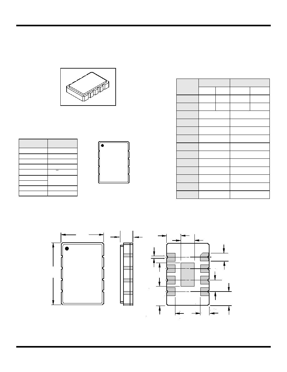
SMC-08
∑
Quartz SAW Stabilized and Filtered "Diff Sine" Technology
∑
Fundamental-Mode Oscillation at 663.552 MHz
∑
Voltage Tunable for Phase Lock Loop Operations
∑
Optical Timing Reference for Forward Error Correction Applications
The output of this device is generated and filtered by narrowband quartz SAW elements at 663.552 MHz. The
configuration of this clock is intended to provide a pure signal for optical timing applications in noisy signal
environments. The Q/Qbar differential output swing of ±1 volt about 0 vdc has symmetry better than ±1% into
loads from 40 ohms to 70 ohms; determined by customer application. The long term frequency accuracy is
set by an external reference source allowing this device to complete a Phase Lock Loop design without the
usual noise and jitter problems associated with PLL's.
Absolute Maximum Ratings
Rating
Value
Units
DC Suppy Voltage
0 to 5.5
VDC
Tune Voltage
0 to 6
VDC
Case Temperature
-55 to 100
∞C
663.552 MHz
Optical
Timing Clock
OP4010B
CAUTION: Electrostatic Sensitive Device. Observe precautions for handling. COCOM CAUTION: Approval by the U.S. Department of Commerce is
required prior to export of this device.
Notes:
1.
Unless otherwise noted, all specifications include any combination of load VSWR, Vcc, and temperature, with Q and Q terminated into
50 ohm loads to ground (see typical test circuit).
2.
Useful tuning range is in excess of what is required over temp, aging, pushing, pulling & accuracy.
3.
The design, manufacturing process, and specifications of this device are subject to change without notice.
4.
Only under the nominal conditions of 50
load impedance with VSWR
1.2 and nominal power supply voltage.
5.
Symmetry is defined as the pulse width (in percent of total period) measured at the 50% points of Q or Q (see timing definitions).
6.
Jitter and other spurious outputs induced by externally generated electrical noise on V
CC
or mechanical vibration are not included in this
specification, except where noted. External voltage regulation and careful PCB layout are recommended for optimum performance.
7.
Applies to period jitter of Q and Q. Measurements are made with the Tektronix CSA803 signal analyzer with at least 1000 samples.
8.
Linearity is a function of the percentage variation from a permitted linear deviation versus the amount of frequency tune range
(see lin-
earity definition).
9.
One or more of the following United States patents apply: 4,616,197; 4,670,681; 4,760,352.
BLOCK DIAGRAM
Q
VCC
Buffer Amplifier
SAW Oscillator
_
Vtune
Q