RF Monolithics, Inc.
Phone: (972) 233-2903
Fax: (972) 387-8148
E-mail: info@rfm.com
Page 1 of 2
RFM Europe
Phone: 44 1963 251383
Fax: 44 1963 251510
http://www.rfm.com
©1999 by RF Monolithics, Inc. The stylized RFM logo are registered trademarks of RF Monolithics, Inc.
RO2181B-111601
Electrical Characteristics
Characteristic
Sym
Notes
Minimum
Typical
Maximum
Units
Frequency (+25 ∞C)
Nominal Frequency
f
C
2, 3, 4, 5
868.275
868.35
868.425
MHz
Tolerance from 868.35 MHz
Df
C
±75
kHz
Insertion Loss
IL
2, 5, 6
2
dB
Quality Factor
Unloaded Q
Q
U
5, 6, 7
18,568
50
Loaded Q
Q
L
1,337
Temperature Stability
Turnover Temperature
T
O
6, 7, 8
-40
25
+85
∞C
Turnover Frequency
f
O
f
C+
16
Frequency Temperature Coefficient
FTC
0.032
ppm/∞C
2
Frequency Aging
Absolute Value during the First Year
|fA|
1
10
ppm/yr
DC Insulation Resistance between Any Two Terminals
5
1.0
M
RF Equivalent RLC Model
Motional Resistance
R
M
5, 6, 7, 9
69.80
Motional Inductance
L
M
38.38
µH
Motional Capacitance
C
M
0.875
fF
Shunt Static Capacitance
C
O
5, 6, 7, 9
2.59
pF
Test Fixture Shunt Inductance
L
TEST
2, 7
11.85
nH
Lid Symbolization (in Addition to Lot and/or Date Code)
296
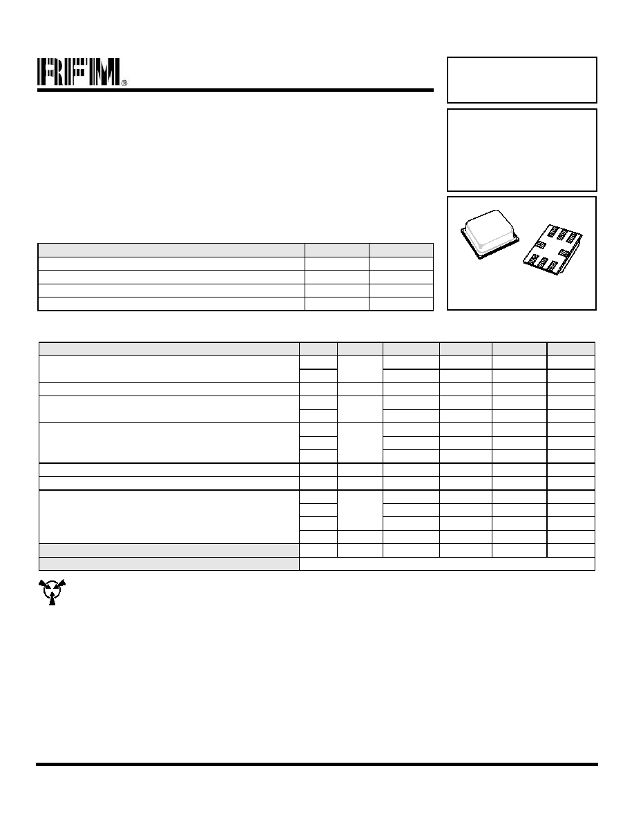
SM5248-8 Case
∑
Very Low Series Resistance
∑
Quartz Stability
∑
Surface-Mount, Solder Seal Package with 4.8 x 5.2 mm Footprint
The RO2181B is a true one-port, surface-acoustic-wave (SAW) resonator in a surface-mount ceramic case.
It provides reliable, fundamental-mode, quartz frequency stabilization.
Absolute Maximum Ratings
Rating
Value
Units
CW RF Power Dissipation
+0
dBm
DC Voltage Between Terminals (Observe ESD Precautions)
±30
VDC
Case Temperature
-40 to +85
∞C
Soldering Temperature
+250
∞C
868.35 MHz
SAW
Resonator
RO2181B
CAUTION: Electrostatic Sensitive Device. Observe precautions for handling.
Notes:
1.
Frequency aging is the change in f
C
with time and is specified at +65∞C or less.
Aging may exceed the specification for prolonged temperatures above +65∞C.
Typically, aging is greatest the first year after manufacture, decreasing in subse-
quent years.
2.
The frequency, f
C
, is measured at the minimum insertion loss point, IL
MIN
, with
the resonator in the 50
test system (VSWR
1.2:1). The shunt inductance,
L
TEST
, is tuned for parallel resonance with C
O
at f
C
. Typically, f
OSCILLATOR
or
f
TRANSMITTER
is approximately equal to the resonator f
C
.
3.
One or more of the following United States patents apply: 4,454,488 and
4,616,197.
4.
Typically, equipment utilizing this device requires emissions testing and govern-
ment approval, which is the responsibility of the equipment manufacturer.
5.
Unless noted otherwise, case temperature T
C
= +25∞C±5∞C.
6.
The design, manufacturing process, and specifications of this device are subject
to change without notice.
7.
Derived mathematically from one or more of the following directly measured
parameters: f
C
, IL, 3 dB bandwidth, f
C
versus T
C
, and C
O
.
8.
Turnover temperature, T
O
, is the temperature of maximum (or turnover) fre-
quency, f
O
. The nominal frequency at any case temperature, T
C
, may be calcu-
lated from: f = f
O
[1 - FTC (T
O
-T
C
)
2
]. Typically,
oscillator T
O
is approximately
equal to the specified
resonator T
O
.
9.
This equivalent RLC model approximates resonator performance near the reso-
nant frequency and is provided for reference only. The capacitance C
O
is the
static (nonmotional) capacitance between the two terminals measured at low
frequency (10 MHz) with a capacitance meter. The measurement includes para-
sitic capacitance with "NC" pads unconnected. Case parasitic capacitance is
approximately 0.05 pF. Transducer parallel capacitance can be calculated as:
C
P
C
O
- 0.05 pF.
868.35 MHz SAW Resonator
RF Monolithics, Inc.
Phone: (972) 233-2903
Fax: (972) 387-8148
E-mail: info@rfm.com
Page 2 of 2
RFM Europe
Phone: 44 1963 251383
Fax: 44 1963 251510
http://www.rfm.com
©1999 by RF Monolithics, Inc. The stylized RFM logo are registered trademarks of RF Monolithics, Inc.
RO2181B-111601
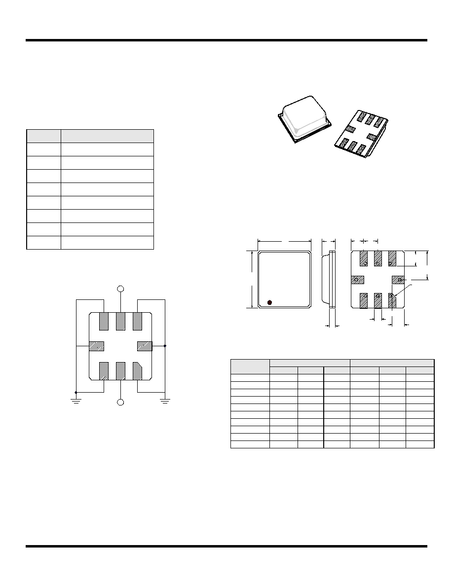
Electrical Connections
This one-port, eight-terminal solder seal resonator is bidirectional. Howev-
er, impedances and circuit board parasitics may not be symmetrical, requir-
ing slightly different oscillator component-matching values.
Typical Circuit
Case Design
Pin
Connection
1
Ground
2
Input or Output
3
Ground
4
Ground
5
Ground
6
Output or Input
7
Ground
8
Ground
5
6
7
4
8
3
2
1
Input or Output
Input or Output
1, 3, 4, 5, 7, 8 No Internal Connection
45∞
C
B
A
D
F
G
I
H
E
3
2
4
7
8
5
6
1
TOP VIEW
BOTTOM VIEW
J
Dimensions
Millimeters
Inches
Min
Nom
Max
Min
Nom
Max
A
5.21
5.33
5.46
0.205
0.210
0.215
B
4.83
4.95
5.08
0.190
0.195
0.200
C
0.38
0.51
0.64
0.015
0.020
0.025
D
1.07
1.19
1.32
0.042
0.047
0.052
E
1.14
1.27
1.40
0.045
0.050
0.055
F
0.58
0.71
0.84
0.023
0.028
0.033
G
1.07
1.19
1.32
0.042
0.047
0.052
H
1.32
1.45
1.57
0.052
0.057
0.062
I
2.54
2.67
2.79
0.100
0.105
0.110
J
1.52
1.78
2.03
0.060
0.070
0.080