 | –≠–ª–µ–∫—Ç—Ä–æ–Ω–Ω—ã–π –∫–æ–º–ø–æ–Ω–µ–Ω—Ç: RXC101 | –°–∫–∞—á–∞—Ç—å:  PDF PDF  ZIP ZIP |
rev04
1
RF Monolithics, Inc.
4441 Sigma Road
Dallas, Texas 75244
(800) 704-6079 toll-free in U.S. and Canada
www.rfm.com
Email: info@rfm.com
Complies with Directive 2002/95/EC (RoHS)
Product Overview
RXC101 is a highly integrated single chip, zero-IF, multi-channel, low
power, high data rate RF receiver designed to operate in the unlicensed
315/433/868 and 915 MHz frequency bands. All critical RF and baseband
functions are completely integrated in the chip, thus minimizing external
component count and simplifying design-ins. Its small size with low power
consumption makes it ideal for various short range radio applications.
The RXC101 supports two modes ≠ Micro controller mode and Standalone
mode. In the Micro controller mode, the use of a generic 10MHz crystal
and a low-cost microcontroller is all that is needed to create a complete
Receiver link. Simple short range radio applications can be supported by
using the RXC101 in the Standalone mode, which allows complete receiver
operation without the use of a microcontroller.
Key Features
∑
Modulation: OOK/FSK (Frequency Hopping Spread Spectrum
capability)
∑
Operating frequency: 315/433/868/915 MHz
∑
High Sensitivity: (-113dBm)
∑
Low current consumption (RX current ~ 8mA)
∑
Wide Operating supply voltage: 2.2 to 5.4V
∑
Low standby current (0.1uA)
∑
FSK Data rate up to 256kbps
∑
Support for Multiple Channels
∑
[315/433 Bands]: 380 Channels (25kHz)
∑
[868 Band]: 761 Channels (25kHz)
∑
[915 Band]: 1040 Channels (25kHz)
∑
Generic 10MHz Xtal reference
∑
Processor or Standalone Operation Mode
∑
Automatic Frequency Alignment
∑
Programmable Analog/Digital Baseband Filter
∑
Programmable
Data
Rate
∑
Programmable Input LNA Gain
∑
Programmable Clock Output Frequency
∑
Programmable Wake-up Timer with programmable Duty Cycle
∑
Programmable Crystal Load Capacitance
∑
Programmable, Positive/Negative FSK Deviation
∑
Programmable Push Button Control
∑
Internal Valid Data Recognition
∑
Integrated PLL, IF & Baseband Circuitry
∑
Integrated Selectable Analog/Digital RSSI
∑
Integrated, Programmable Low Battery Voltage Detector
16-TSSOP package
∑
Integrated
Crystal
Oscillator
∑
Integrated
Clock
Recovery
∑
Standard SPI interface
∑
External Wake-up Events
∑
External Processor Interrupt pin
∑
Receive FIFO or External Pin
∑
TTL/CMOS Compatible I/O pins
∑
No Manual Adjustment Needed for Production
∑
Very few external components requirement
∑
Small size plastic package: 16-pin TSSOP
∑
Standard 13 inch reel, 2000 pieces.
Popular applications
∑
Remote control applications
∑
Active RFID tags
∑
Wireless PC Peripherals
∑
Automated Meter reading
∑
Home & Industrial Automation
∑
Security
systems
∑
Remote keyless entry
∑
Automobile
Immobilizers
∑
Sports & Performance monitoring
∑
Wireless
Toys
∑
Medical
equipment
∑
Low power two way telemetry systems
∑
Wireless mesh sensors
∑
Wireless
modules

2
Table of Contents
Table of Contents
.......................................................................................................... 2
1. RXC101 Pin Description
........................................................................................... 3
1.1 Processor Mode Pin Configuration ...................................................................... 3
1.2 Simple Mode Pin Configuration............................................................................ 4
2. RXC101 Functional Description
............................................................................... 5
2.1 RXC101 Typical Application Circuit ..................................................................... 5
Processor Mode .................................................................................................. 5
Antenna Design Considerations........................................................................... 6
PCB Layout Considerations................................................................................. 6
2.2
Simple Mode ........................................................................................................ 9
Simple Mode Functional Block Diagram .............................................................. 9
Duty Cycle Mode ............................................................................................... 11
3. RXC101 Functional Characteristics
....................................................................... 12
Input
Amplifier .......................................................................................................... 12
Baseband Data and Filtering ................................................................................... 12
Data Quality Detector (DQD) ................................................................................... 13
Valid Data Detector (DDET)..................................................................................... 13
Receiver
FIFO.......................................................................................................... 13
Receive Signal Strength Indicator (RSSI) ................................................................ 13
Automatic Frequency Adjustment (AFA).................................................................. 14
Crystal
Oscillator...................................................................................................... 14
Frequency Control (PLL) and Frequency Synthesizer ............................................. 14
Wake-Up
Mode ........................................................................................................ 15
Low
Battery
Detector ............................................................................................... 15
SPI
Interface ............................................................................................................ 15
SPI Interface Timing.......................................................................................... 15
4. Control and Configuration Registers
.................................................................... 16
Status
Register ....................................................................................................... 16
Configuration
Register [POR=893Ah] ...................................................................... 17
Receiver Control Register [POR=C0C1h] ................................................................ 19
FIFO Configuration Register [POR=CE89h] ............................................................ 21
Automatic Frequency Adjust Register [POR=C6F7h] .............................................. 22
Baseband Filter Register [POR=C42Ch].................................................................. 24
Frequency Setting Register [POR=A680h] .............................................................. 25
Data Rate Setup Register [POR=C823h]................................................................. 26
Wake-up Timer Period Register [POR=E196h]........................................................ 27
Duty Cycle Set Register [POR=CC0Eh] .................................................................. 28
Battery Detect Threshold and Clock Output Register [POR=C200h] ....................... 29
5. Maximum Ratings
.................................................................................................... 30
Recommended
Operating Ratings........................................................................... 30
6. DC Electrical Characteristics
................................................................................ 30
7. AC Electrical Characteristics
................................................................................ 31
8. Package Information
.............................................................................................. 33
3
1. Pin Description
Processor Mode
Pin Name
Description
1
SDI
SPI Data In
2
SCK
SPI Data Clock
3 nCS
Chip Select Input
≠ Selects the chip for an SPI data transaction. The pin must be pulled `low'
for a 16-bit read or write function. See Figure 6 for timing specifications.
4 nFINT/SDO
FIFO Interrupt Output (active low)
≠ When the internal FIFO is enabled (
Configuration
Register,
Bit [6]), this pin acts as a FIFO Fill interrupt indicating that the FIFO has filled to its
pre-programmed limit (
FIFO Configuration Register
, Bit [7..4]).
SPI Serial Data Out
≠ May be used to read out the
Status Register
contents.
5 nIRQ
Interrupt Request Output
≠ Any of the following events will generate an external interrupt:
-Wake-up timer timeout
-Low Battery Detect
-FIFO fill
-FIFO overflow
To determine the source of the interrupt, the processor may read the first four bits of the
Status Register
.
6 DATA/nFSEL
Data Output
≠ Received data can be taken from this pin when the FIFO is not used.
FIFO Select Input
≠ When the FIFO is used this pin selects the FIFO when data is to be read
out over the SDO pin.
7
DCLK/FCAP/
FINT
Data Recovery Clock
Output
≠ Recovered Data clock Output (FIFO not used).
Filter Capacitor
≠ When the analog filter is used this pin is the connection for the RC
lowpass filter. The corner frequency should be set as close to the data rate as possible to
retain good sensitivity.
FIFO Interrupt Output (active high)
≠ Indicates when there are remaining bits in the FIFO to
be read. Set the FIFO Fill level to 1 in the
FIFO Configuration Register
.
8 ClkOut
Optional host processor Clock Output. Frequency programmable through the
Battery Detect
Threshold and Clock Output Register.
9 Xtal/Ref
Xtal
- Connects to a 10MHz series crystal or an external oscillator reference.
The circuit
contains an integrated load capacitor (See
Configuration Register
) in order to minimize the
external component count. The crystal is used as the reference for the PLL, which generates
the local oscillator frequency. The accuracy requirements for production tolerance,
temperature drift and aging can be determined from the maximum allowable local oscillator
frequency error. Whenever a low frequency error is essential for the application, it is possible
to "pull" the crystal to the accurate frequency by changing the load capacitor value.
Ext Ref
≠ An external reference, such as an oscillator, may be connected as a reference
source. Connect through a .01uF capacitor.
10 nRST
Reset
Output
(active Low)
11 GND
System Ground
12
RF_P
RF Diff I/O
13
RF_N
RF Diff I/O
14 VDD
Supply Voltage
15 RSSIA
Analog RSSI Output
≠ This pin may be used as an input to an A/D for signal strength or may
be used as a baseband data output for OOK signaling. See
Baseband Filter Register
to
calculate the appropriate filter capacitor value.
16
DDET
Valid Data Detector Output
- (See
Receiver Control Register
for output definition)
1.1 Processor Mode Pin Configuration
SDI
SCK
nCS
SDO/FINT
IRQ
DATA/nFSEL
CR/FINT/FCAP
CLKOUT
DDET
RSSIA
VDD
RF_N
RF_P
GND
nRESET
Xtal/Ref
TOP VIEW
RXC101
2
3
4
5
6
7
8
9
10
11
12
13
14
15
16
1

4
Simple Mode
Pin Name
Description
1
FS0
Frequency Select Bit 0
2
BS0
Band Select Bit 0
3
BS1
Band Select Bit 1
4 DO1
Digital Output 1
≠ May be connected to an LED or other device.
5 DO2
Digital Output 2
≠ May be connected to an LED or other device.
6 DO3
Digital Output 3
≠ May be connected to an LED or other device.
7 DO4
Digital Output 4
≠ May be connected to an LED or other device.
8 Mode/DCM
Mode Select
≠ Sets the device in Processor or Simple Mode. When the chip powers
on it checks the state of this pin and determines what mode to select. When this pin
is connected to VDD, the chip enters Simple Mode.
(Low Power) Duty Cycle Mode
-
9 Xtal/Ref
Xtal
≠ Connects to a 10MHz series crystal or an external oscillator reference.
Ext Ref
≠ An external reference, such as an oscillator, may be connected as a
reference source. Connect through a .01uF capacitor.
10
FS1
Frequency Select Bit 1
11 GND
System Ground
12 RF_P
RF Signal Input
13
RF_N
RF Signal Input
14 VDD
Supply Voltage
15
FS2
Frequency Select Bit 2
16
FS3
Frequency Select Bit 3
1.2 Simple Mode Pin Configuration
FS0
BS0
BS1
DO1
DO2
DO3
DO4
Mode/DCM
FS3
FS2
VDD
RF_N
RF_P
GND
FS1
Xtal/Ref
TOP VIEW
RXC101
2
3
4
5
6
7
8
9
10
11
12
13
14
15
16
1
5
2. Functional Description
The RXC101 is a low power, frequency agile, zero-IF, multi-channel FSK receiver for use in the 315, 433,
868, and 916 MHz bands. All RF and baseband functions are completely integrated requiring only a
single 10MHz crystal as a reference source and an external low-cost processor. Functions include:
∑
PLL
synthesizer
∑
LNA, programmable gain
∑
I/Q
Mixers
∑
I/Q
Demodulators
∑
Baseband
Filters
∑
Baseband
Amplifiers
∑
RSSI
∑
Low
Battery
Detector
∑
Wake-up Timer/Duty Cycle Mode
∑
Valid Data Detection/Data Quality
The RXC101 is ideal for Frequency Hopping Spread Spectrum (FHSS) applications requiring frequency
agility to meet FCC requirements. The RXC101 supports use of a low-cost microcontroller, or may
operate as a single chip solution for simple applications. The RXC101 also incorporates different sleep
modes to reduce overall current consumption and extend battery life. It is ideal for applications operating
from typical lithium coin cells.
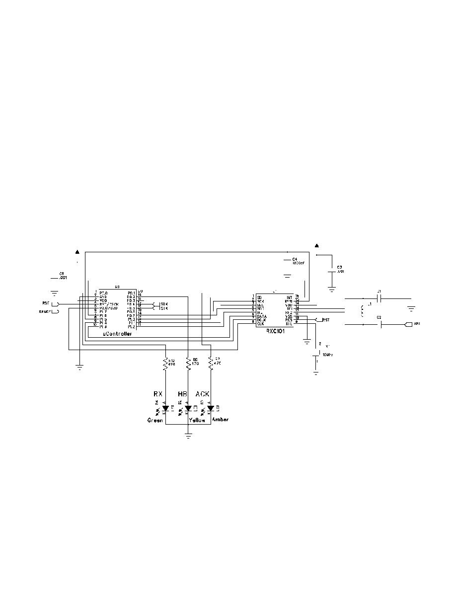
2.1 RXC101 Typical Application Circuit
Figure 1. Typical Processor Mode Application Circuit
Processor Mode (Application Circuit)
The RF pins are high impedance and differential. The optimum differential load for the RF port is 250
Ohms. Antennas ideally suited for this would be a Dipole, Folded Dipole, and Loop. A single ended 50
Ohm connection may also be used with the matching circuit given in Figure 1. Matching component
values for each band are given in Table 16.