RF Monolithics, Inc.
Phone: (972) 233-2903
Fax: (972) 387-9148
E-mail: info@rfm.com
Page 1 of 5
RFM Europe
Phone: 44 1963 251383
Fax: 44 1963 251510
http://www.rfm.com
©2001 by RF Monolithics, Inc. The stylized RFM logo are registered trademarks of RF Monolithics, Inc.
SF1097A-051205
Electrical Characteristics
Characteristic
Sym
Notes
Min
Typ
Max
Units
Nominal Center Frequency
f
C
1
71.000
MHz
Passband
Insertion Loss at fc
IL
6.5
9.0
dB
2 dB Passband
BW
2
1, 2
±90
kHz
3 dB Passband
BW
3
±110
Group Delay Variation over fc ±90 kHz
GDV
500
1500
ns
P-P
Rejection
fc-350 to fc-250 and fc+250 to fc+250 kHz
1, 2, 3
5
dB
fc-500 to fc-350 and fc+350 to fc+500 kHz
20
fc-700 to fc-500 and fc+500 to fc+700 kHz
30
fc-2500 to fc-700 and fc+700 to fc+2500 kHz
35
Ultimate 10 MHz to fc-2.5 MHz and fc+2.5 MHz to 130 MHz
40
Except spurious responses at 1.05, 1.6, 1.8, & 2 x fc
35
Operating Temperature Range
T
A
1
-20
+80
∞C
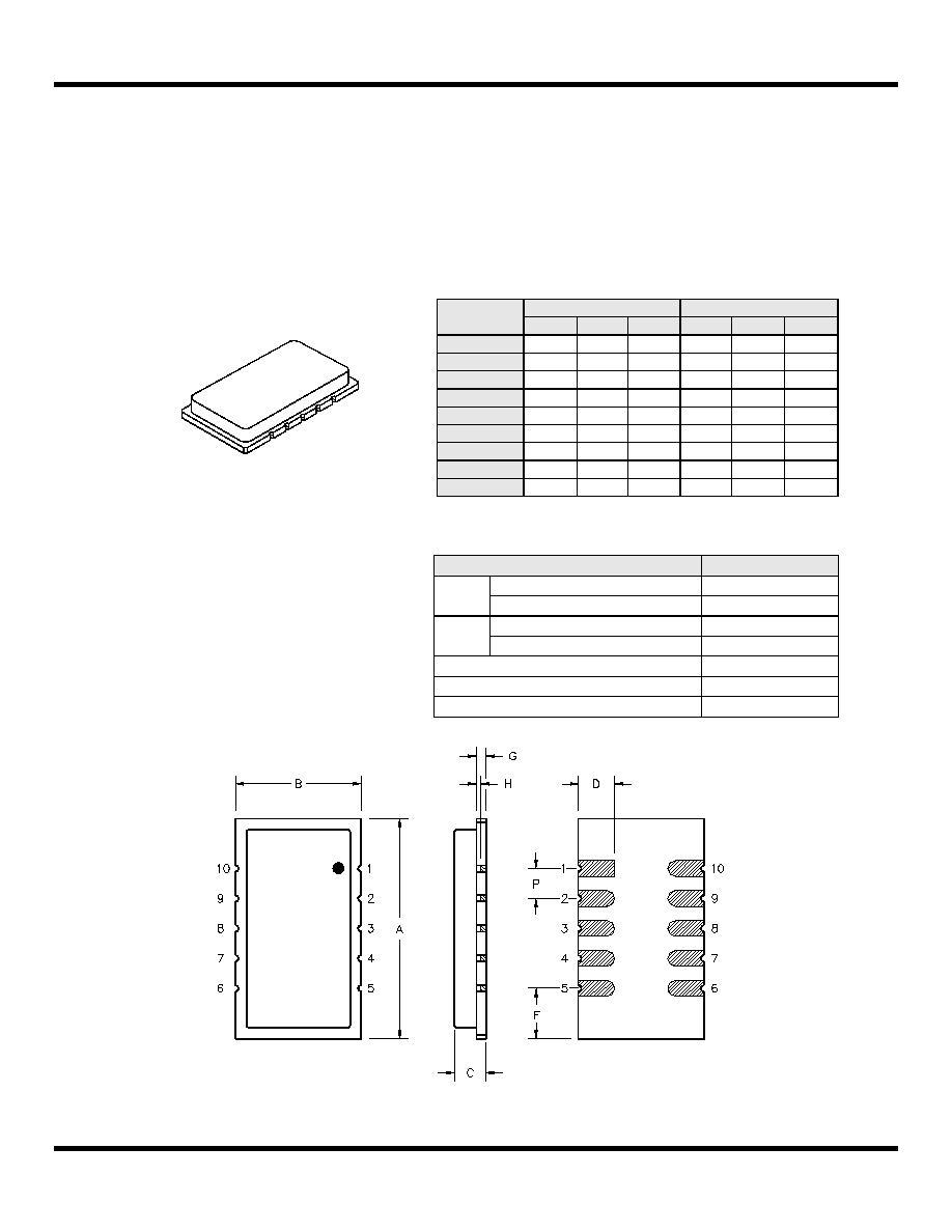
SMP-08
∑
Designed for GSM Terminal IF Applications
∑
Excellent Size-to-Performance Ratio
∑
Hermetic 14 x 8 mm Surface-Mount Case
Absolute Maximum Ratings
Rating
Value
Units
Maximum Incident Power in Passband
+20
dBm
Max. DC voltage between any 2 terminals
30
VDC
Storage Temperature Range
-40 to +85
∞C
Max. Soldering Profile
235∞C for 90 s
71 MHz
SAW Filter
SF1097A
Notes:
1.
Unless noted otherwise, all specifications apply over the operating temperature range
with filter soldered to the specified demonstration board with impedance matching to 50 W
and measured with 50
network analyzer.
2.
Unless noted otherwise, all frequency specifications are referenced to the nominal center
frequency, fc.
3.
Rejection is measured as attenuation below the minimum IL point in the passband.
Rejection in final user application is dependent on PCB layout and external impedance
matching design. See Application Note No. 42 for details.
4.
"LRIP" or "L" after the part number indicates "low rate initial production" and "ENG" or "E"
indicates "engineering prototypes."
5.
The design, manufacturing process, and specifications of this filter are subject to change.
6.
Either Port 1 or Port 2 may be used for either input or output in the design. However,
impedances and impedance matching may vary between Port 1 and Port 2, so that the fil-
ter must always be installed in one direction per the circuit design.
7.
US and international patents may apply.
8.
Electrostatic Sensitive Device. Observe precautions for handling.
Connection
Terminals
Port 1
1, 10
Port 2
5, 6
Case Ground
All others
Electrical Connections
Case Style
SMP-08 14 x 8 mm Nominal Footprint
Lid Symbolization (YY = year, WW = week)
RFM SF1097A YYWW