 | –≠–ª–µ–∫—Ç—Ä–æ–Ω–Ω—ã–π –∫–æ–º–ø–æ–Ω–µ–Ω—Ç: TR3001 | –°–∫–∞—á–∞—Ç—å:  PDF PDF  ZIP ZIP |
1
Æ
Rating
Value
Units
Power Supply and All Input/Output Pins
-0.3 to +4.0
V
Non-Operating Case Temperature
-50 to +100
o
C
Soldering Temperature (10 seconds)
250
o
C
Characteristic
Sym
Notes
Minimum
Typical
Maximum
Units
Operating Frequency
f
O
314.80
315.20
MHz
Modulation Type
OOK/ASK
OOK Data Rate
30
kbps
ASK Data Rate
115.2
kbps
Receiver Performance, High Sensitivity Mode
Sensitivity, 2.4 kbps, 10-3 BER, AM Test Method
1
-109
dBm
Sensitivity, 2.4 kbps, 10-3 BER, Pulse Test Method
1
-103
dBm
Current, 2.4 kbps (R
PR
= 330 K)
2
3.0
mA
Sensitivity, 19.2 kbps, 10-3 BER, AM Test Method
1
-105
dBm
Sensitivity, 19.2 kbps, 10-3 BER, Pulse Test Method
1
-99
dBm
Current, 19.2 kbps (R
PR
= 330 K)
2
3.1
mA
Sensitivity, 115.2 kbps, 10-3 BER, AM Test Method
1
-101
dBm
Sensitivity, 115.2 kbps, 10-3 BER, Pulse Test Method
1
-95
dBm
Current, 115.2 kbps
3.8
mA
Receiver Performance, Low Current Mode
Sensitivity, 2.4 kbps, 10-3 BER, AM Test Method
1
-104
dBm
Sensitivity, 2.4 kbps, 10-3 BER, Pulse Test Method
1
-98
dBm
Current, 2.4 kbps (R
PR
= 1100 K)
2
1.8
mA
Receiver Out-of-Band Rejection, ±5% f
O
R
±5%
3
80
dB
Receiver Ultimate Rejection
R
ULT
3
100
dB
Electrical Characteristics (typical values given for 3.0 Vdc power supply, 25
o
C)
Absolute Maximum Ratings
∑ Designed for Short-Range Wireless Data Communications
∑ Supports RF Data Transmission Rates Up to 115.2 kbps
∑ 3 V, Low Current Operation plus Sleep Mode
∑ Stable, Easy to Use, Low External Parts Count
TR3001
315.00 MHz
Hybrid
Transceiver
The TR3001 hybrid transceiver is ideal for short-range wireless data applications where robust
operation, small size, low power consumption and low cost are required. The TR3001 employs
RFM's amplifier-sequenced hybrid (ASH) architecture to achieve this unique blend of character-
istics. All critical RF functions are contained in the hybrid, simplifying and speeding design-in.
The receiver section of the TR3001 is sensitive and stable. A wide dynamic range log detector,
in combination with digital AGC and a compound data slicer, provide robust performance in the
presence of on-channel interference or noise. Two stages of SAW filtering provide excellent re-
ceiver out-of-band rejection. The transmitter includes provisions for both on-off keyed (OOK)
and amplitude-shift keyed (ASK) modulation. The transmitter employs SAW filtering to suppress
output harmonics, facilitating compliance with FCC Part 15 and similar regulations.
2
Electrical Characteristics (typical values given for 3.0 Vdc power supply, 25
o
C)
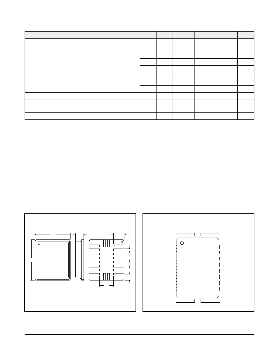
S M - 2 0 L P a c k a g e D r a w i n g
0 . 0 8 "
( 2 . 0 3 )
0 . 1 2 5 "
( 3 . 2 0 )
0 . 0 2 "
( 0 . 5 1 )
0 . 0 4 "
( 1 . 0 2 )
0 . 1 3 "
( 3 . 3 0 )
0 . 4 3 "
( 1 0 . 9 )
0 . 3 8 "
( 9 . 6 5 )
0 . 0 7 5 "
( 1 . 9 0 )
3
4
5
6
7
9
1 1
1 2
1 3
1 4
1 5
1 6
1 7
1 9
A S H T r a n s c e i v e r P i n O u t
R F I O
8
2
1 0
2 0
1
1 8
L P F A D J
R R E F
T H L D 2
A G C C A P
P K D E T
B B O U T
C M P I N
R X D A T A
T X M O D
T H L D 1
P R A T E
P W I D T H
G N D 1
V C C 1
G N D 2
V C C 2
G N D 3
C N T R L 0
C N T R L 1
Notes:
1. Typical sensitivity data is based on a 10
-3
bit error rate (BER), using DC-balanced data. There are two test methods commonly used to
measure OOK/ASK receiver sensitivity, the "100% AM" test method and the "Pulse" test method. Sensitivity data is given for both test meth-
ods. See Appendix 3.8 in the ASH Transceiver Designer's Guide for the details of each test method, and for sensitivity curves for a 2.2 to
3.7 V supply voltage range at five operating temperatures. The application/test circuit and component values are shown on the next page and
in the Designer's Guide.
2. At low data rates it is possible to adjust the ASH pulse generator to trade-off some receiver sensitivity for lower operating current. Sensitiv-
ity data and receiver current are given at 2.4 kbps for both high sensitivity operation (R
PR
= 330 K) and low current operation (R
PR
= 1100 K).
3. Data is given with the ASH radio matched to a 50 ohm load. Matching component values are given on the next page.
4. See Table 1 on Page 8 for additional information on ASH radio event timing.
Characteristic
Sym
Notes
Minimum
Typical
Maximum
Units
Transmitter Performance
Peak RF Output Power, 250 µA TXMOD Current
P
O
3
1.5
dBm
Peak Current, 250 µA TXMOD Current
I
TP
3
9.5
mA
2
nd
- 4
th
Harmonic Output
3
-50
dBm
5
th
- 10
th
Harmonic Outputs
3
-55
dBm
Non-harmonic Spurious Outputs
3
-50
dBm
OOK Turn On/Turn Off Times
t
ON
/t
OFF
4
12/6
µs
ASK Output Rise/Fall Times
t
TR
/t
TF
4
1.1/1.1
µs
Sleep Mode Current
I
S
0.7
µA
Power Supply Voltage Range
V
CC
2.2
3.7
Vdc
Power Supply Voltage Ripple
10
mV
P-P
Ambient Operating Temperature
T
A
-40
85
o
C

Item
Symbol
OOK
OOK
ASK
Units
Notes
Encoded Data Rate
DR
NOM
2.4
19.2
115.2
kbps
see pages 1 & 2
Minimum Signal Pulse
SP
MIN
416.67
52.08
8.68
µs
single bit
Maximum Signal Pulse
SP
MAX
1666.68
208.32
34.72
µs
4 bits of
same value
AGCCAP Capacitor
C
AGC
-
-
2200
pF
±10% ceramic
PKDET Capacitor
C
PKD
-
-
0.001
µF
±10% ceramic
BBOUT Capacitor
C
BBO
0.1
0.015
0.0027
µF
±10% ceramic
BBOUT Resistor
R
BBO
12
0
0
K
±5%
LPFAUX Capacitor
C
LPF
0.0047
-
-
µF
±5%
TXMOD Resistor
R
TXM
8.2
8.2
8.2
K
±5%, for 1.5 dBm output
LPFADJ Resistor
R
LPF
330
100
15
K
±5%
RREF Resistor
R
REF
100
100
100
K
±1%
THLD2 Resistor
R
TH2
-
-
100
K
±1%, for 6 dB below peak
THLD1 Resistor
R
TH1
0
0
10
K
±1%, typical values
PRATE Resistor
R
PR
330
330
160
K
±5%
PWIDTH Resistor
R
PW
270 to GND
270 to GND
1000 to Vcc
K
±5%
DC Bypass Capacitor
C
DCB
4.7
4.7
4.7
µF
tantalum
RF Bypass Capacitor 1
C
RFB1
100
100
100
pF
±5% NPO
RF Bypass Capacitor 2
C
RFB2
100
100
100
pF
±5% NPO
RF Bypass Bead
L
RFB
Fair-Rite
Fair-Rite
Fair-Rite
vendor
2506031217YO or equivalent
Series Tuning Inductor
L
AT
82
82
82
nH
50 ohm antenna
Shunt Tuning/ESD Inductor
L
ESD
33
33
33
nH
50 ohm antenna
3
M o d u l a t i o n I n p u t
D a t a O u t p u t
T O P V I E W
G N D
3
C N T
R L 0
C N T
R L 1
P
W I D T H
P
R A T E
T H L D
1
T H L D
2
R R E F
G N D 2
T X
M O D
R X
D A T A
L P F
A D J
C M P
I N
B B
O U T
P K
D E T
A G C
C A P
V C C
1
V C C
2
R F I O
G N D 1
+ 3
V D C
A S H T r a n s c e i v e r A p p l i c a t i o n C i r c u i t
O O K C o n f i g u r a t i o n
1
2 0
2
3
4
5
6
7
8
9
1 0
1 1
1 2
1 3
1 4
1 5
1 6
1 7
1 8
1 9
+ 3
V D C
R
P W
R
P R
R
T H 1
R
T H 2
R
R E F
R
L P F
R
T X M
C
B B O
C
R F B 2
C
D C B
L
A T
L
E S D
C
R F B 1
L
R F B
+
T / R
C
L P F
R
B B O
M o d u l a t i o n I n p u t
D a t a O u t p u t
T O P V I E W
G N D
3
C N T
R L 0
C N T
R L 1
P
W I D T H
P
R A T E
T H L D
1
T H L D
2
R R E F
G N D 2
T X
M O D
R X
D A T A
L P F
A D J
C M P
I N
B B
O U T
P K
D E T
A G C
C A P
V C C
1
V C C
2
R F I O
G N D 1
+ 3
V D C
A S H T r a n s c e i v e r A p p l i c a t i o n C i r c u i t
A S K C o n f i g u r a t i o n
1
2 0
2
3
4
5
6
7
8
9
1 0
1 1
1 2
1 3
1 4
1 5
1 6
1 7
1 8
1 9
+ 3
V D C
T R M o d e
C o n t r o l
R
P W
R
P R
R
T H 1
R
T H 2
R
R E F
R
L P F
R
T X M
C
B B O
C
P K D
C
A G C
C
R F B 2
C
D C B
L
A T
L
E S D
C
R F B 1
L
R F B
+
Transceiver Set-Up, 3.0 Vdc, -40 to +85
0
C
CAUTION: Electrostatic Sensitive Device. Observe precautions when handling.
4
ASH Transceiver Theory of Operation
Introduction
RFM's amplifier-sequenced hybrid (ASH) transceiver is specifically
designed for short-range wireless data communication applications.
The transceiver provides robust operation, very small size, low
power consumption and low implementation cost. All critical RF
functions are contained in the hybrid, simplifying and speeding de-
sign-in. The ASH transceiver can be readily configured to support a
wide range of data rates and protocol requirements. The transceiver
features excellent suppression of transmitter harmonics and virtually
no RF emissions when receiving, making it easy to certify to short-
range (unlicensed) radio regulations.
Amplifier-Sequenced Receiver Operation
The ASH transceiver's unique feature set is made possible by its
system architecture. The heart of the transceiver is the amplifier-
sequenced receiver section, which provides more than 100 dB of
stable RF and detector gain without any special shielding or de-
coupling provisions. Stability is achieved by distributing the total RF
gain over time. This is in contrast to a superheterodyne receiver,
which achieves stability by distributing total RF gain over multiple
frequencies.
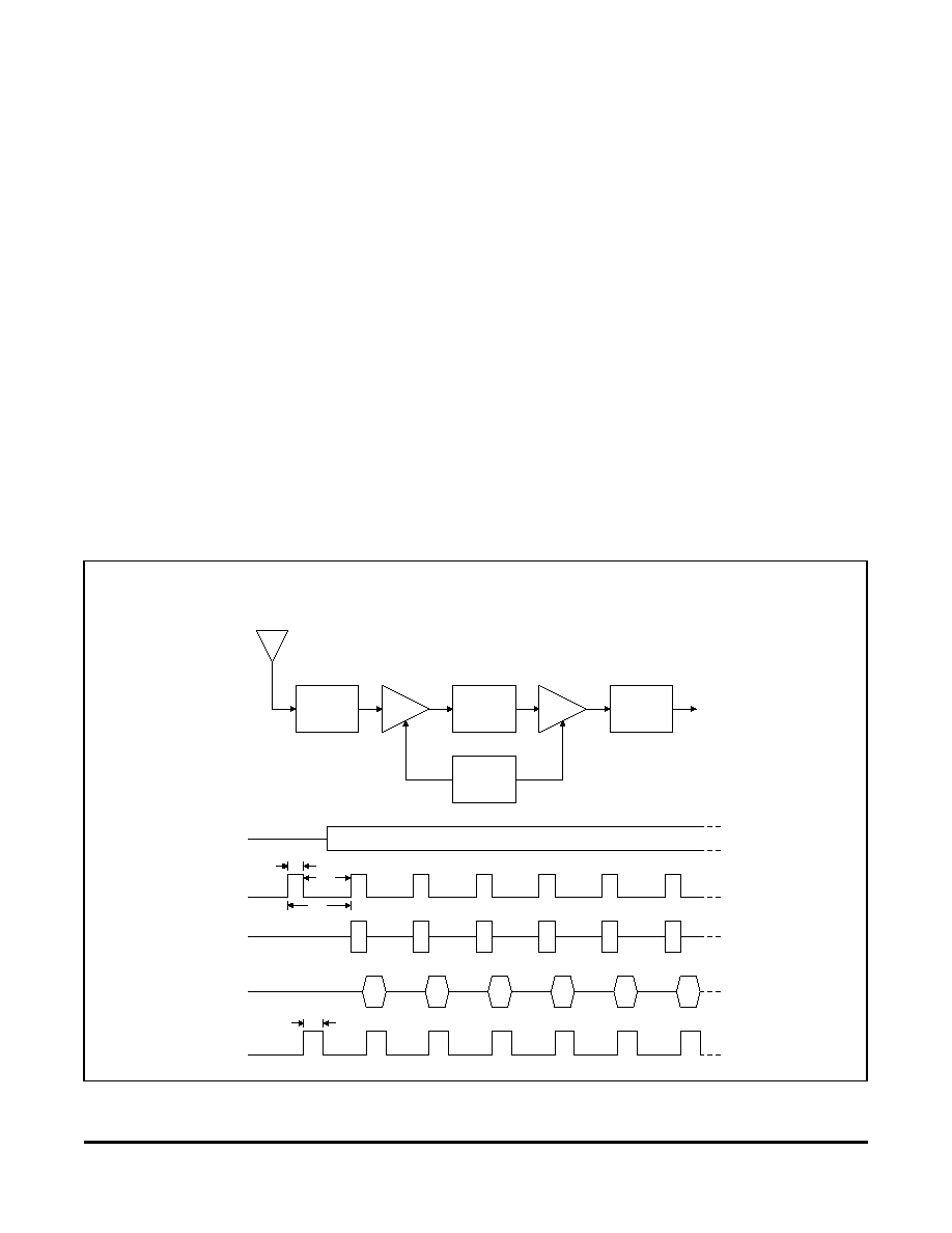
Figure 1 shows the basic block diagram and timing cycle for an am-
plifier-sequenced receiver. Note that the bias to RF amplifiers RFA1
and RFA2 are independently controlled by a pulse generator, and
that the two amplifiers are coupled by a surface acoustic wave
(SAW) delay line, which has a typical delay of 0.5 µs.
An incoming RF signal is first filtered by a narrow-band SAW filter,
and is then applied to RFA1. The pulse generator turns RFA1 ON
for 0.5 µs. The amplified signal from RFA1 emerges from the SAW
delay line at the input to RFA2. RFA1 is now switched OFF and
RFA2 is switched ON for 0.55 µs, amplifying the RF signal further.
The ON time for RFA2 is usually set at 1.1 times the ON time for
RFA1, as the filtering effect of the SAW delay line stretches the sig-
nal pulse from RFA1 somewhat. As shown in the timing diagram,
RFA1 and RFA2 are never on at the same time, assuring excellent
receiver stability. Note that the narrow-band SAW filter eliminates
sampling sideband responses outside of the receiver passband, and
the SAW filter and delay line act together to provide very high re-
ceiver ultimate rejection.
Amplifier-sequenced receiver operation has several interesting char-
acteristics that can be exploited in system design. The RF amplifiers
in an amplifier-sequenced receiver can be turned on and off almost
instantly, allowing for very quick power-down (sleep) and wake-up
times. Also, both RF amplifiers can be off between ON sequences
to trade-off receiver noise figure for lower average current consump-
tion. The effect on noise figure can be modeled as if RFA1 is on
continuously, with an attenuator placed in front of it with a loss
equivalent to 10*log
10
(RFA1 duty factor), where the duty factor is the
average amount of time RFA1 is ON (up to 50%). Since an
amplifier-sequenced receiver is inherently a sampling receiver, the
overall cycle time between the start of one RFA1 ON sequence and
A S H R e c e i v e r B l o c k D i a g r a m & T i m i n g C y c l e
A n t e n n a
P u l s e
G e n e r a t o r
S A W
D e l a y L i n e
S A W F i l t e r
R F A 1
R F A 2
D a t a
O u t
D e t e c t o r &
L o w - P a s s
F i l t e r
R F D a t a P u l s e
P 1
P 2
R F A 1 O u t
R F I n p u t
P 1
D e l a y L i n e
O u t
P 2
t
P W 2
t
P W 1
t
P R I
t
P R C
Figure 1
5
the start of the next RFA1 ON sequence should be set to sample
the narrowest RF data pulse at least 10 times. Otherwise, significant
edge jitter will be added to the detected data pulse.
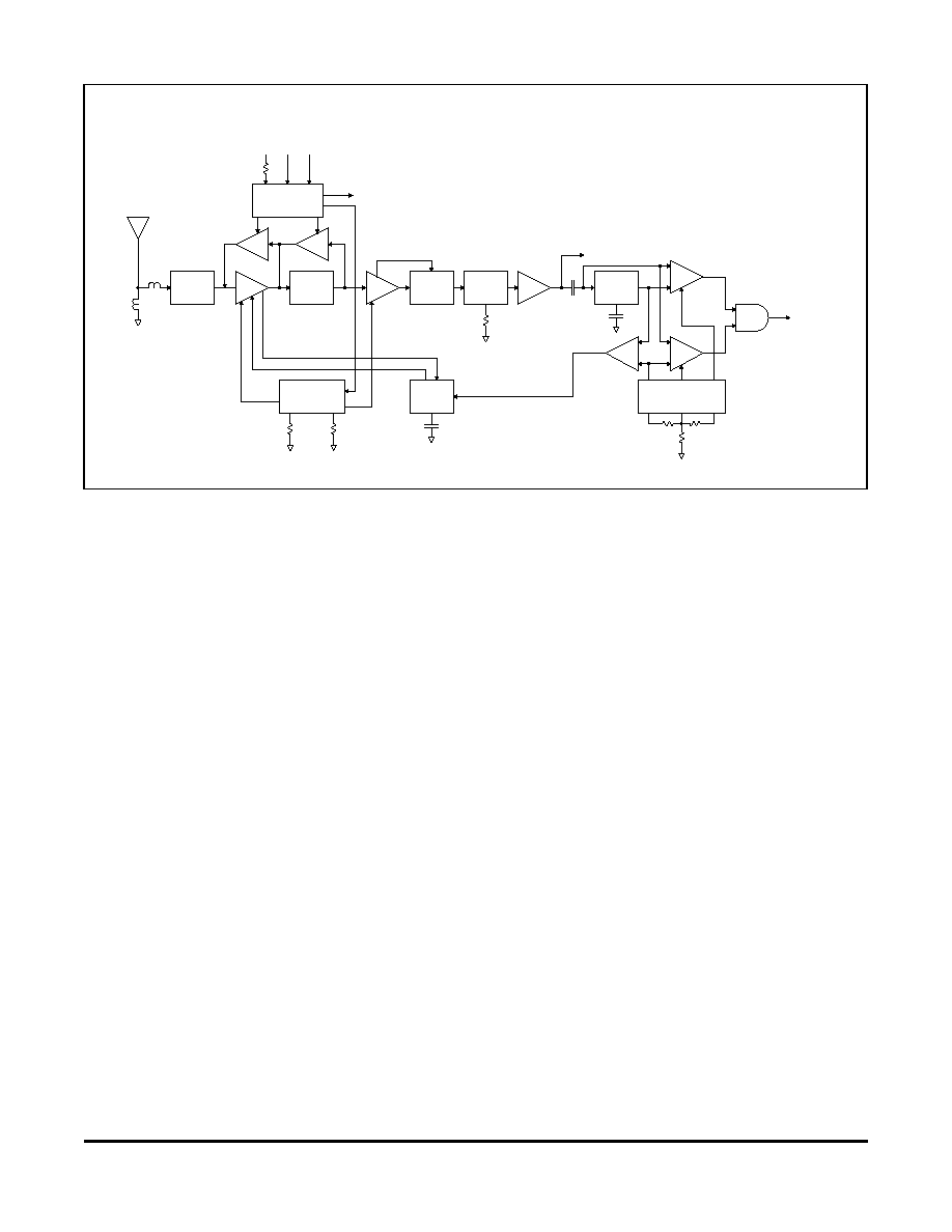
ASH Transceiver Block Diagram
Figure 2 is the general block diagram of the ASH transceiver.
Please refer to Figure 2 for the following discussions.
Antenna Port
The only external RF components needed for the transceiver are
the antenna and its matching components. Antennas presenting an
impedance in the range of 35 to 72 ohms resistive can be satisfacto-
rily matched to the RFIO pin with a series matching coil and a shunt
matching/ESD protection coil. Other antenna impedances can be
matched using two or three components. For some impedances,
two inductors and a capacitor will be required. A DC path from RFIO
to ground is required for ESD protection.
Receiver Chain
The output of the SAW filter drives amplifier RFA1. This amplifier in-
cludes provisions for detecting the onset of saturation (AGC Set),
and for switching between 35 dB of gain and 5 dB of gain (Gain Se-
lect). AGC Set is an input to the AGC Control function, and Gain Se-
lect is the AGC Control function output. ON/OFF control to RFA1
(and RFA2) is generated by the Pulse Generator & RF Amp Bias
function. The output of RFA1 drives the SAW delay line, which has
a nominal delay of 0.5 µs.
The second amplifier, RFA2, provides 51 dB of gain below satura-
tion. The output of RFA2 drives a full-wave detector with 19 dB of
threshold gain. The onset of saturation in each section of RFA2 is
detected and summed to provide a logarithmic response. This is
added to the output of the full-wave detector to produce an overall
detector response that is square law for low signal levels, and tran-
sitions into a log response for high signal levels. This combination
provides excellent threshold sensitivity and more than 70 dB of
detector dynamic range. In combination with the 30 dB of AGC
range in RFA1, more than 100 dB of receiver dynamic range is
achieved.
The detector output drives a gyrator filter. The filter provides a
three-pole, 0.05 degree equiripple low-pass response with excellent
group delay flatness and minimal pulse ringing. The 3 dB bandwidth
of the filter can be set from 4.5 kHz to 1.8 MHz with an external re-
sistor.
The filter is followed by a base-band amplifier which boosts the de-
tected signal to the BBOUT pin. When the receiver RF amplifiers
are operating at a 50%-50% duty cycle, the BBOUT signal changes
about 10 mV/dB, with a peak-to-peak signal level of up to 685 mV.
For lower duty cycles, the mV/dB slope and peak-to-peak signal
level are proportionately less. The detected signal is riding on a
1.1 Vdc level that varies somewhat with supply voltage, tempera-
ture, etc. BBOUT is coupled to the CMPIN pin or to an external data
recovery process (DSP, etc.) by a series capacitor. The correct
value of the series capacitor depends on data rate, data run length,
and other factors as discussed in the ASH Transceiver Designer's
Guide.
When an external data recovery process is used with AGC, BBOUT
must be coupled to the external data recovery process and CMPIN
by separate series coupling capacitors. The AGC reset function is
driven by the signal applied to CMPIN.
When the transceiver is placed in power-down (sleep) or in a trans-
mit mode, the output impedance of BBOUT becomes very high. This
feature helps preserve the charge on the coupling capacitor to mini-
mize data slicer stabilization time when the transceiver switches
back to the receive mode.
Data Slicers
The CMPIN pin drives two data slicers, which convert the analog
signal from BBOUT back into a digital stream. The best data slicer
choice depends on the system operating parameters. Data slicer
DS1 is a capacitively-coupled comparator with provisions for an ad-
justable threshold. DS1 provides the best performance at low
A S H T r a n s c e i v e r B l o c k D i a g r a m
R F A 1
R F A 2
T X A 1
T X A 2
S A W
D e l a y L i n e
S A W
C R F i l t e r
L o g
A n t e n n a
R F I O
T u n i n g / E S D
D e t e c t o r
L o w - P a s s
F i l t e r
B B
A G C
C o n t r o l
P e a k
D e t e c t o r
P u l s e G e n e r a t o r
& R F A m p B i a s
L P F A D J
P R A T E
P W I D T H
R X D A T A
T X M O D
C N
T R L 1
C N
T R L 0
A G C C A P
R
R E F
T H L D 2
T H L D 1
M o d u l a t i o n
& B i a s C o n t r o l
P o w e r D o w n
C o n t r o l
G a i n S e l e c t
A G C S e t
A G C R e s e t
T h r e s h o l d
C o n t r o l
B B O U T
D S 2
D S 1
A N D
d B B e l o w
P e a k T h l d
R e f
T h l d
P K D E T
R e f
A G C
C
B B O
C
P K D
R
L P F
C
A G C
R
P R
R
P W
R
T H 2
R
T H 1
R
T X M
2 0
8
1 7
1 8
1 4
1 5
3
9
5
6
4
7
1 3
1 1
1 2
V C C 1 : P i n 2
V C C 2 : P i n 1 6
G N D 1 : P i n 1
G N D 2 : P i n 1 0
G N D 3 : P i n 1 9
R R E F : P i n 1 1
C M P I N : P i n 6
T X
I N
T u n i n g
Figure 2