 | –≠–ª–µ–∫—Ç—Ä–æ–Ω–Ω—ã–π –∫–æ–º–ø–æ–Ω–µ–Ω—Ç: TR3005 | –°–∫–∞—á–∞—Ç—å:  PDF PDF  ZIP ZIP |
1
Rating
Value
Units
Power Sup ply and All In put/Out put Pins
-0.3 to +4.0
V
Non-Operating Case Tem per a ture
-50 to +100
o
C
Sol dering Tem per a ture (10 sec onds)
250
o
C
Characteristic
Sym
Notes
Minimum
Typical
Maximum
Units
Op er ating Fre quency Range
f
O
403.35
403.65
MHz
Fre quency Drift, -10 to 45
o
C, 2.2 to 3.7 Vdc
±100
ppm
Mod u la tion Type
OOK/ASK
OOK Data Rate
30
kbps
ASK Data Rate
115.2
kbps
Re ceiver Per for mance, High Sen si tiv ity Mode
Sen si tiv ity, 2.4 kbps, 10-3 BER, AM Test Method
1
-109
dBm
Sen si tiv ity, 2.4 kbps, 10-3 BER, Pulse Test Method
1
-103
dBm
Cur rent, 2.4 kbps (R
PR
= 330 K)
2
3.0
mA
Sen si tiv ity, 19.2 kbps, 10-3 BER, AM Test Method
1
-105
dBm
Sen si tiv ity, 19.2 kbps, 10-3 BER, Pulse Test Method
1
-99
dBm
Cur rent, 19.2 kbps (R
PR
= 330 K)
2
3.1
mA
Sen si tiv ity, 115.2 kbps, 10-3 BER, AM Test Method
1
-101
dBm
Sen si tiv ity, 115.2 kbps, 10-3 BER, Pulse Test Method
1
-95
dBm
Cur rent, 115.2 kbps
3.8
mA
Re ceiver Per for mance, Low Current Mode
Sen si tiv ity, 2.4 kbps, 10-3 BER, AM Test Method
1
-104
dBm
Sen si tiv ity, 2.4 kbps, 10-3 BER, Pulse Test Method
1
-98
dBm
Cur rent, 2.4 kbps (R
PR
= 1100 K)
2
1.8
mA
Re ceiver Out-of-Band Re jec tion, ±5% f
O
R
±5%
3
80
dB
Elec tri cal Char ac ter is tics (typ i cal val ues given for 3.0 Vdc power sup ply, 25
o
C)
Ab so lute Max i mum Rat ings
∑
De signed for Short-Range Wire less Med i cal Data Com mu ni ca tions
∑
Sup ports RF Data Trans mis sion Rates Up to 115.2 kbps
∑
3 V, Low Cur rent Op er a tion plus Sleep Mode
TR3005
403.50 MHz
Hybrid
Transceiver
The TR3005 ul tra-miniature hy brid trans ceiver is ideal for short-range wire less med i cal data ap -
pli ca tions where ro bust op er a tion, small size, low power con sump tion and low cost are re quired.
The TR3005 em ploys RFM's am pli fier-sequenced hy brid (ASH) ar chi tec ture to achieve this
unique blend of char ac teristics. All crit i cal RF func tions are con tained in the hy brid, sim pli fy ing
and speed ing de sign-in. The re ceiver sec tion of the TR3005 is sen si tive and sta ble. A wide dy -
namic range log de tec tor, in com bi na tion with dig i tal AGC and a com pound data slicer, pro vide
ro bust per for mance in the pres ence of on-channel in ter fer ence or noise. Two stages of SAW fil -
ter ing pro vide ex cel lent re ceiver out-of-band re jec tion. The trans mit ter in cludes pro vi sions for
both on-off keyed (OOK) and amplitude-shift keyed (ASK) mod u la tion. The trans mit ter em ploys
SAW fil ter ing to sup press out put har mon ics.
2
Elec tri cal Char ac ter is tics (typ i cal val ues given for 3.0 Vdc power sup ply, 25
o
C)
3
4
5
6
7
9
11
12
13
14
15
16
17
19
ASH Transceiver Pin Out
RFIO
8
2
10
20
1
18
LPFADJ
RREF
THLD2
AGCCAP
PKDET
BBOUT
CMPIN
RXDATA
TXMOD
THLD1
PRATE
PWIDTH
GND1
VCC1
GND2
VCC2
GND3
CNTRL0
CNTRL1
Notes:
1. Typ i cal sen si tiv ity data is based on a 10
-3
bit er ror rate (BER), us ing DC-balanced data. There are two test meth ods com monly used to
mea sure OOK/ASK re ceiver sen si tiv ity, the "100% AM" test method and the "Pulse" test method. Sen si tiv ity data is given for both test meth -
ods. See Ap pen dix 3.8 in the ASH Trans ceiver De signer's Guide for the de tails of each test meth od, and for sen si tiv ity curves for a 2.2 to
3.7 V sup ply voltage range at five op er at ing tem per a tures. The ap pli ca tion/test circuit and com po nent val ues are shown on the next page and
in the De signer's Guide.
2. At low data rates it is pos si ble to ad just the ASH pulse gen er a tor to trade-off some re ceiver sen si tiv ity for lower op er at ing cur rent. Sen si tiv -
ity data and re ceiver cur rent are given at 2.4 kbps for both high sen si tiv ity op er a tion (R
PR
= 330 K) and low cur rent op er a tion (R
PR
= 1100 K).
3. Data is given with the ASH ra dio matched to a 50 ohm load. Matching com po nent val ues are given on the next page.
4. See Ta ble 1 on Page 8 for ad di tional in for ma tion on ASH ra dio event tim ing.
Characteristic
Sym
Notes
Minimum
Typical
Maximum
Units
Trans mit ter Performance
Peak RF Out put Power, 250 µA TXMOD Current
P
O
3
0
dBm
Peak Cur rent, 250 µA TXMOD Current
I
TP
3
7.5
mA
2
nd
- 4
th
Har monic Out put
3
-50
dBm
5
th
- 10
th
Har monic Out puts
3
-55
dBm
Non-harmonic Spu ri ous Outputs
3
-55
dBm
OOK Turn On/Turn Off Times
t
ON
/t
OFF
4
12/6
µs
ASK Out put Rise/Fall Times
t
TR
/t
TF
4
1.1/1.1
µs
Sleep Mode Current
I
S
0.7
µA
Power Sup ply Volt age Range
V
CC
2.2
3.7
Vdc
Power Sup ply Volt age Ripple
10
mV
P-P
Am bi ent Op er ating Tem per a ture
T
A
-10
55
o
C
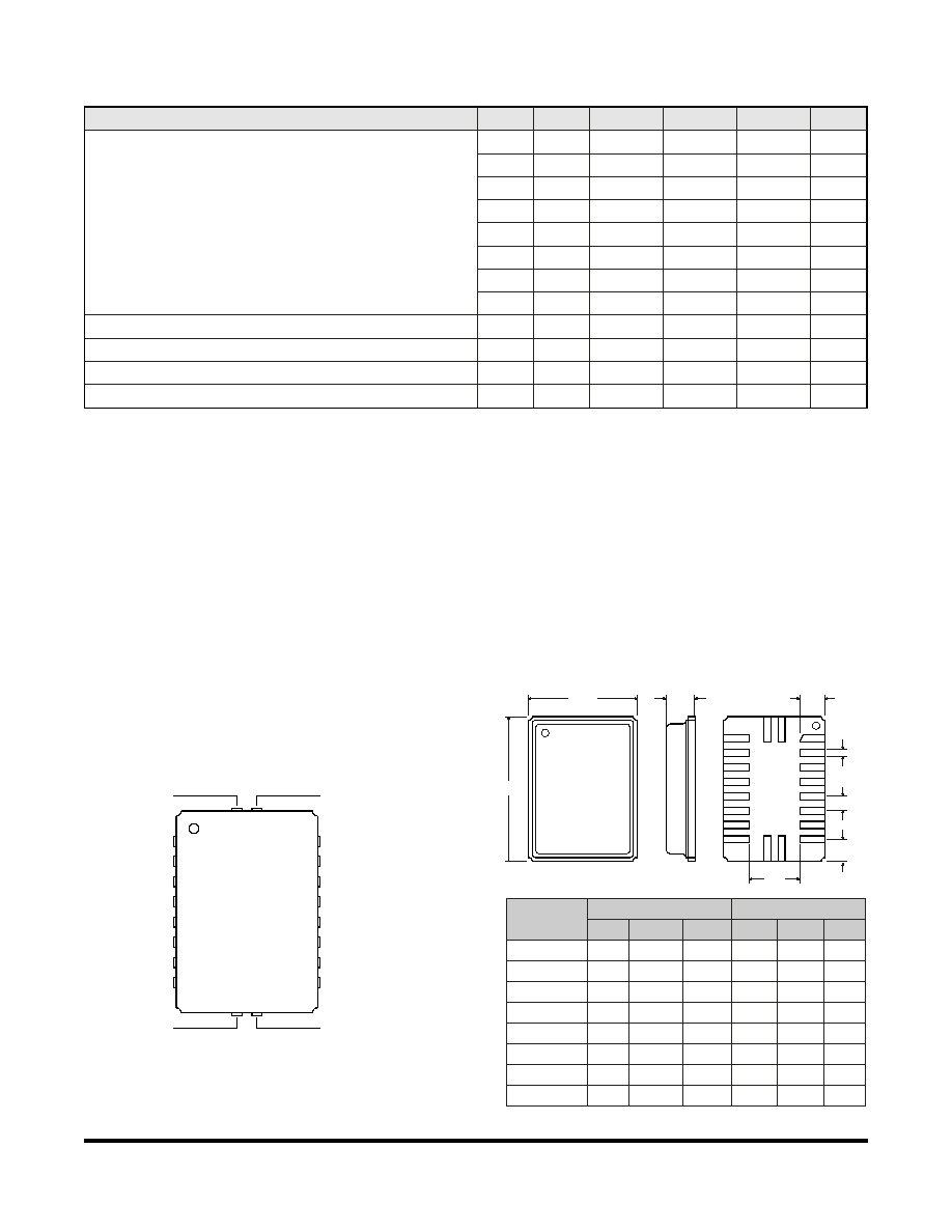
SM-20H Package Drawing
C
D
E
F
G
A
B
H
Di men sion
mm
Inches
Min
Nom
Max
Min
Nom
Max
A
9.881
10.033
10.135
.389
.395
.400
B
6.731
6.858
6.985
.265
.270
.275
C
1.778
1.930
2.032
.070
.076
.080
D
1.651
1.778
1.905
.065
.070
.075
E
0.381
0.508
0.635
.015
.020
.025
F
0.889
1.016
1.143
.035
.040
.045
G
3.175
3.302
3.429
.0125
.130
.135
H
1.397
1.524
1.651
.055
.060
.065
Item
Sym bol
OOK
OOK
ASK
Units
Notes
En coded Data Rate
DR
NOM
2.4
19.2
115.2
kbps
see pages 1 & 2
Min i mum Signal Pulse
SP
MIN
416.67
52.08
8.68
µs
sin gle bit
Max i mum Sig nal Pulse
SP
MAX
1666.68
208.32
34.72
µs
4 bits of same value
AGCCAP Ca pac i tor
C
AGC
-
-
2200
pF
±10% ce ramic
PKDET Ca pac i tor
C
PKD
-
-
0.001
µF
±10% ce ramic
BBOUT Ca pac i tor
C
BBO
0.1
0.015
0.0027
µF
±10% ce ramic
BBOUT Re sis tor
R
BBO
12
0
0
K
±5%
LPFAUX Ca pac i tor
C
LPF
0.0047
-
-
µF
±5%
TXMOD Re sis tor
R
TXM
8.2
8.2
8.2
K
±5%, for 0 dBm out put
LPFADJ Re sis tor
R
LPF
330
100
15
K
±5%
RREF Re sis tor
R
REF
100
100
100
K
±1%
THLD2 Re sis tor
R
TH2
-
-
100
K
±1%, for 6 dB be low peak
THLD1 Re sis tor
R
TH1
0
0
10
K
±1%, typical values
PRATE Re sis tor
R
PR
330
330
160
K
±5%
PWIDTH Re sis tor
R
PW
270 to GND
270 to GND
1000 to Vcc
K
±5%
DC By pass Ca pac i tor
C
DCB
4.7
4.7
4.7
µF
tantalum
RF By pass Ca pac i tor 1
C
RFB1
100
100
100
pF
±5% NPO
RF By pass Ca pac i tor 2
C
RFB2
100
100
100
pF
±5% NPO
RF By pass Bead
L
RFB
Fair-Rite
Fair-Rite
Fair-Rite
vendor
2506033017YO or equivalent
Series Tuning In duc tor
L
AT
56
56
56
nH
50 ohm an tenna
Shunt Tuning/ESD Inductor
L
ESD
220
220
220
nH
50 ohm an tenna
3
Modulation Input
Data Output
TOP VIEW
GND
3
CNT
RL0
CNT
RL1
P
WIDTH
P
RATE
THLD
1
THLD
2
RREF
GND2
TX
MOD
RX
DATA
LPF
ADJ
CMP
IN
BB
OUT
PK
DET
AGC
CAP
VCC
1
VCC
2
RFIO
GND1
+ 3
VDC
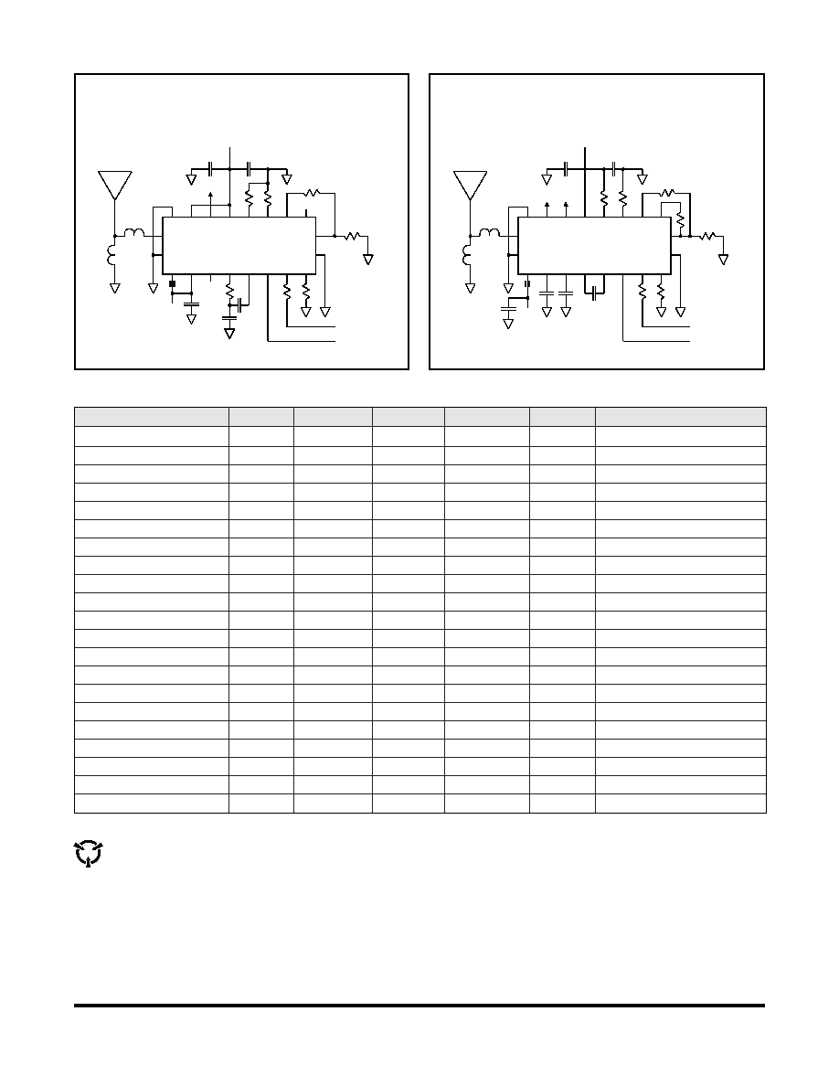
ASH Transceiver Application Circuit
OOK Configuration
1
20
2
3
4
5
6
7
8
9
10
11
12
13
14
15
16
17
18
19
+ 3
VDC
R
PW
R
PR
R
TH1
R
REF
R
LPF
R
TXM
C
BBO
C
RFB2
C
DCB
L
AT
L
ESD
C
RFB1
L
RFB
+
T/R
C
LPF
R
BBO
Modulation Input
Data Output
TOP VIEW
GND
3
CNT
RL0
CNT
RL1
P
WIDTH
P
RATE
THLD
1
THLD
2
RREF
GND2
TX
MOD
RX
DATA
LPF
ADJ
CMP
IN
BB
OUT
PK
DET
AGC
CAP
VCC
1
VCC
2
RFIO
GND1
+ 3
VDC
ASH Transceiver Application Circuit
ASK Configuration
1
20
2
3
4
5
6
7
8
9
10
11
12
13
14
15
16
17
18
19
+ 3
VDC
TR Mode
Control
R
PW
R
PR
R
TH1
R
TH2
R
REF
R
LPF
R
TXM
C
BBO
C
PKD
C
AGC
C
RFB2
C
DCB
L
AT
L
ESD
C
RFB1
L
RFB
+
Trans ceiver Set-Up, 3.0 Vdc, -40 to +85
0
C
CAUTION: Elec tro static Sen si tive De vice. Ob serve pre cau tions when han dling.
4
ASH Transceiver Theory of Operation
In tro duc tion
RFM's am pli fier-sequenced hy brid (ASH) trans ceiver is spe cif i cally
de signed for short-range wire less data com mu ni ca tion ap pli ca tions.
The trans ceiver pro vides ro bust op er a tion, very small size, low
power con sump tion and low im ple men ta tion cost. All crit i cal RF
func tions are con tained in the hy brid, sim pli fy ing and speed ing de -
sign-in. The ASH trans ceiver can be readily con fig ured to sup port a
wide range of data rates and pro to col re quire ments. The trans ceiver
fea tures ex cel lent sup pres sion of trans mit ter har mon ics and vir tu ally
no RF emis sions when re ceiv ing, mak ing it easy to cer tify to short-
range (unli censed) ra dio reg u la tions.
Am pli fier-Sequenced Re ceiver Op er a tion
The ASH trans ceiver's unique fea ture set is made pos si ble by its
sys tem ar chi tec ture. The heart of the trans ceiver is the am pli fier-
sequenced re ceiver sec tion, which pro vides more than 100 dB of
sta ble RF and de tec tor gain with out any spe cial shield ing or de -
coup ling pro vi sions. Sta bil ity is achieved by dis trib ut ing the to tal RF
gain over time. This is in con trast to a super het ero dyne re ceiver,
which achieves sta bil ity by dis trib ut ing to tal RF gain over mul ti ple
fre quen cies.
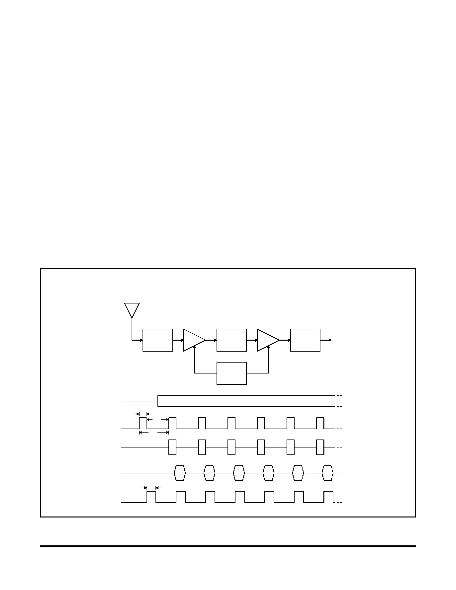
Fig ure 1 shows the ba sic block di a gram and tim ing cy cle for an am -
pli fier-sequenced re ceiver. Note that the bias to RF am pli fi ers RFA1
and RFA2 are in de pend ently con trolled by a pulse gen er a tor, and
that the two am pli fi ers are cou pled by a sur face acous tic wave
(SAW) de lay line, which has a typ i cal de lay of 0.5 µs.
An in com ing RF sig nal is first fil tered by a nar row-band SAW fil ter,
and is then ap plied to RFA1. The pulse gen er a tor turns RFA1 ON
for 0.5 µs. The am pli fied sig nal from RFA1 emerges from the SAW
de lay line at the in put to RFA2. RFA1 is now switched OFF and
RFA2 is switched ON for 0.55 µs, am pli fy ing the RF sig nal fur ther.
The ON time for RFA2 is usu ally set at 1.1 times the ON time for
RFA1, as the fil ter ing ef fect of the SAW de lay line stretches the sig -
nal pulse from RFA1 some what. As shown in the tim ing di a gram,
RFA1 and RFA2 are never on at the same time, as sur ing ex cel lent
re ceiver sta bil ity. Note that the nar row-band SAW fil ter elim i nates
sam pling side band re sponses out side of the re ceiver passband, and
the SAW fil ter and de lay line act to gether to pro vide very high re -
ceiver ul ti mate re jec tion.
Am pli fier-sequenced re ceiver op er a tion has sev eral in ter est ing char -
ac ter is tics that can be ex ploited in sys tem de sign. The RF am pli fi ers
in an am pli fier-sequenced re ceiver can be turned on and off al most
in stantly, al low ing for very quick power-down (sleep) and wake-up
times. Also, both RF am pli fi ers can be off be tween ON se quences
to trade-off re ceiver noise fig ure for lower av er age cur rent con sump -
tion. The ef fect on noise fig ure can be mod eled as if RFA1 is on
con tin u ously, with an at tenu ator placed in front of it with a loss
equiv a lent to 10*log
10
(RFA1 duty fac tor), where the duty fac tor is the
av er age amount of time RFA1 is ON (up to 50%). Since an
amplifier-sequenced re ceiver is in her ently a sam pling re ceiver, the
over all cy cle time be tween the start of one RFA1 ON se quence and
ASH Receiver Block Diagram & Timing Cycle
Antenna
Pulse
Generator
SAW
Delay Line
SAW Filter
RFA1
RFA2
Data
Out
Detector &
Low-Pass
Filter
RF Data Pulse
P1
P2
RFA1 Out
RF Input
P1
Delay Line
Out
P2
t
PW2
t
PW1
t
PRI
t
PRC
Figure 1
5
the start of the next RFA1 ON se quence should be set to sam ple
the nar row est RF data pulse at least 10 times. Oth er wise, sig nif i cant
edge jit ter will be added to the de tected data pulse.
ASH Trans ceiver Block Di a gram
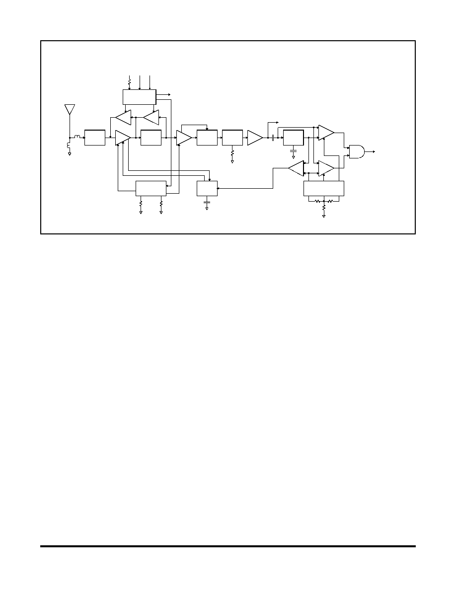
Fig ure 2 is the gen eral block di a gram of the ASH trans ceiver.
Please re fer to Fig ure 2 for the fol low ing dis cus sions.
An tenna Port
The only ex ter nal RF com po nents needed for the trans ceiver are
the an tenna and its match ing com po nents. An tennas pre sent ing an
im ped ance in the range of 35 to 72 ohms re sis tive can be sat is fac to -
rily matched to the RFIO pin with a se ries match ing coil and a shunt
match ing/ESD pro tec tion coil. Other an tenna im ped ances can be
matched us ing two or three com po nents. For some im ped ances,
two in duc tors and a ca pac i tor will be re quired. A DC path from RFIO
to ground is required for ESD pro tec tion.
Re ceiver Chain
The out put of the SAW fil ter drives am pli fier RFA1. This am pli fier in -
cludes pro vi sions for de tect ing the on set of sat u ra tion (AGC Set),
and for switch ing be tween 35 dB of gain and 5 dB of gain (Gain Se -
lect). AGC Set is an in put to the AGC Con trol func tion, and Gain Se -
lect is the AGC Con trol func tion out put. ON/OFF con trol to RFA1
(and RFA2) is gen er ated by the Pulse Gen er a tor & RF Amp Bias
func tion. The out put of RFA1 drives the SAW de lay line, which has
a nom i nal de lay of 0.5 µs.
The sec ond am pli fier, RFA2, pro vides 51 dB of gain be low sat u ra -
tion. The out put of RFA2 drives a full-wave de tec tor with 19 dB of
thresh old gain. The on set of sat u ra tion in each sec tion of RFA2 is
de tected and summed to pro vide a log a rith mic re sponse. This is
added to the out put of the full-wave de tec tor to pro duce an over all
de tec tor re sponse that is square law for low sig nal lev els, and tran -
si tions into a log re sponse for high sig nal lev els. This com bi na tion
pro vides ex cel lent thresh old sen si tiv ity and more than 70 dB of
detector dy namic range. In com bi na tion with the 30 dB of AGC
range in RFA1, more than 100 dB of re ceiver dy namic range is
achieved.
The de tec tor out put drives a gyrator fil ter. The fil ter pro vides a
three-pole, 0.05 de gree equiripple low-pass re sponse with ex cel lent
group de lay flat ness and min i mal pulse ring ing. The 3 dB band width
of the fil ter can be set from 4.5 kHz to 1.8 MHz with an ex ter nal re -
sis tor.
The fil ter is fol lowed by a base-band am pli fier which boosts the de -
tected sig nal to the BBOUT pin. When the re ceiver RF am pli fi ers
are op er at ing at a 50%-50% duty cy cle, the BBOUT sig nal changes
about 10 mV/dB, with a peak-to-peak sig nal level of up to 685 mV.
For lower duty cy cles, the mV/dB slope and peak-to-peak sig nal
level are pro por tion ately less. The de tected sig nal is rid ing on a
1.1 Vdc level that var ies some what with sup ply volt age, tem per a -
ture, etc. BBOUT is cou pled to the CMPIN pin or to an ex ter nal data
re cov ery pro cess (DSP, etc.) by a se ries ca pac i tor. The cor rect
value of the se ries ca pac i tor de pends on data rate, data run length,
and other fac tors as dis cussed in the ASH Trans ceiver De signer's
Guide.
When an ex ter nal data re cov ery pro cess is used with AGC, BBOUT
must be cou pled to the ex ter nal data re cov ery pro cess and CMPIN
by sep a rate se ries cou pling ca pac i tors. The AGC re set func tion is
driven by the sig nal ap plied to CMPIN.
When the trans ceiver is placed in power-down (sleep) or in a trans -
mit mode, the out put im ped ance of BBOUT be comes very high. This
fea ture helps pre serve the charge on the cou pling ca pac i tor to min i -
mize data slicer sta bi li za tion time when the trans ceiver switches
back to the re ceive mode.
Data Slicers
The CMPIN pin drives two data slic ers, which con vert the an a log
sig nal from BBOUT back into a digital stream. The best data slicer
choice de pends on the sys tem op er at ing pa ram e ters. Data slicer
DS1 is a ca pac i tively-coupled com para tor with pro vi sions for an ad -
just able thresh old. DS1 pro vides the best per for mance at low
ASH Transceiver Block Diagram
RFA1
RFA2
TXA1
TXA2
SAW
Delay Line
SAW
CR Filter
Log
Antenna
RFIO
Tuning/ESD
Detector
Low-Pass
Filter
BB
AGC
Control
Peak
Detector
Pulse Generator
& RF Amp Bias
LPFADJ
PRATE
PWIDTH
RXDATA
TXMOD
CN
TRL1
CN
TRL0
AGCCAP
R
REF
THLD2
THLD1
Modulation
& Bias Control
Power Down
Control
Gain Select
AGC Set
AGC Reset
Threshold
Control
BBOUT
DS2
DS1
AND
dB Below
Peak Thld
Ref
Thld
PKDET
Ref
AGC
C
BBO
C
PKD
R
LPF
C
AGC
R
PR
R
PW
R
TH2
R
TH1
R
TXM
20
8
17
18
14
15
3
9
5
6
4
7
13
11
12
VCC1: Pin 2
VCC2: Pin 16
GND1: Pin 1
GND2: Pin 10
GND3: Pin 19
RREF: Pin 11
CMPIN: Pin 6
TX
IN
Tuning
Figure 2

sig nal-to-noise con di tions. The thresh old, or squelch, off sets the
com para tor's slic ing level from 0 to 90 mV, and is set with a re sis tor
be tween the RREF and THLD1 pins. This thresh old al lows a trade-
off be tween re ceiver sen si tiv ity and out put noise den sity in the
no-signal con di tion. For best sen si tiv ity, the thresh old is set to 0. In
this case, noise is out put con tin u ously when no sig nal is pres ent.
This, in turn, re quires the cir cuit be ing driven by the RXDATA pin to
be able to pro cess noise (and sig nals) con tin u ously.
This can be a prob lem if RXDATA is driv ing a cir cuit that must
"sleep" when data is not pres ent to con serve power, or when it its
nec es sary to min i mize false in ter rupts to a multitasking pro ces sor.
In this case, noise can be greatly re duced by in creas ing the thresh -
old level, but at the ex pense of sen si tiv ity. The best 3 dB band width
for the low-pass fil ter is also af fected by the thresh old level set ting of
DS1. The band width must be in creased as the thresh old is in -
creased to min i mize data pulse-width vari a tions with sig nal am pli -
tude.
Data slicer DS2 can over come this com pro mise once the sig nal
level is high enough to en able its op er a tion. DS2 is a "dB- below-
peak" slicer. The peak de tec tor charges rap idly to the peak value of
each data pulse, and de cays slowly in be tween data pulses (1:1000
ra tio). The slicer trip point can be set from 0 to 120 mV be low this
peak value with a re sis tor be tween RREF and THLD2. A thresh old
of 60 mV is the most com mon set ting, which equates to "6 dB be low
peak" when RFA1 and RFA2 are run ning a 50%-50% duty cy cle.
Slicing at the "6 dB-below-peak" point re duces the sig nal am pli tude
to data pulse-width vari a tion, al low ing a lower 3 dB fil ter band width
to be used for im proved sen si tiv ity.
DS2 is best for ASK mod u la tion where the trans mit ted wave form
has been shaped to min i mize sig nal band width. How ever, DS2 is
sub ject to be ing tem po rarily "blinded" by strong noise pulses, which
can cause burst data er rors. Note that DS1 is ac tive when DS2 is
used, as RXDATA is the log i cal AND of the DS1 and DS2 out puts.
DS2 can be dis abled by leav ing THLD2 dis con nected. A non-zero
DS1 thresh old is re quired for proper AGC op er a tion.
AGC Con trol
The out put of the Peak De tec tor also pro vides an AGC Re set sig nal
to the AGC Con trol func tion through the AGC com para tor. The pur -
pose of the AGC func tion is to ex tend the dy namic range of the re -
ceiver, so that two trans ceiv ers can op er ate close to gether when
run ning ASK and/or high data rate mod u la tion. The on set of sat u ra -
tion in the out put stage of RFA1 is de tected and gen er ates the AGC
Set sig nal to the AGC Con trol func tion. The AGC Con trol func tion
then se lects the 5 dB gain mode for RFA1. The AGC Com para tor
will send a re set sig nal when the Peak De tec tor out put (mul ti plied by
0.8) falls be low the thresh old volt age for DS1.
A ca pac i tor at the AGCCAP pin avoids AGC "chat ter ing" dur ing the
time it takes for the sig nal to prop a gate through the low-pass fil ter
and charge the peak de tec tor. The AGC ca pac i tor also al lows the
hold-in time to be set lon ger than the peak de tec tor de cay time to
avoid AGC chat ter ing dur ing runs of "0" bits in the re ceived data
stream. Note that AGC op er a tion re quires the peak de tec tor to be
func tion ing, even if DS2 is not be ing used. AGC op er a tion can be
de feated by con nect ing the AGCCAP pin to Vcc. The AGC can be
latched ON once en gaged by con nect ing a 150 kilohm re sis tor be -
tween the AGCCAP pin and ground in lieu of a ca pac i tor.
Re ceiver Pulse Gen er a tor and RF Am pli fier Bias
The re ceiver am pli fier-sequence op er a tion is con trolled by the Pulse
Gen er a tor & RF Am pli fier Bias mod ule, which in turn is con trolled by
the PRATE and PWIDTH in put pins, and the Power Down (sleep)
Con trol Sig nal from the Mod u la tion & Bias Con trol func tion.
In the low data rate mode, the in ter val be tween the fall ing edge of
one RFA1 ON pulse to the ris ing edge of the next RFA1 ON pulse
t
PRI
is set by a re sis tor be tween the PRATE pin and ground. The in -
ter val can be ad justed be tween 0.1 and 5 µs. In the high data rate
mode (se lected at the PWIDTH pin) the re ceiver RF am pli fi ers op er -
ate at a nom i nal 50%-50% duty cy cle. In this case, the start-to-start
pe riod t
PRC
for ON pulses to RFA1 are con trolled by the PRATE re -
sis tor over a range of 0.1 to 1.1 µs.
In the low data rate mode, the PWIDTH pin sets the width of the ON
pulse t
PW1
to RFA1 with a re sis tor to ground (the ON pulse width
t
PW2
to RFA2 is set at 1.1 times the pulse width to RFA1 in the low
data rate mode). The ON pulse width t
PW1
can be ad justed be tween
0.55 and 1 µs. How ever, when the PWIDTH pin is con nected to Vcc
through a 1 M re sis tor, the RF am pli fi ers op er ate at a nom i nal
50%-50% duty cy cle, fa cil i tat ing high data rate op er a tion. In this
case, the RF am pli fi ers are con trolled by the PRATE re sis tor as de -
scribed above.
Both re ceiver RF am pli fi ers are turned off by the Power Down Con -
trol Sig nal, which is in voked in the sleep and trans mit modes.
Trans mit ter Chain
The trans mit ter chain con sists of a SAW de lay line os cil la tor fol -
lowed by a mod u lated buffer am pli fier. The SAW fil ter sup presses
trans mit ter har mon ics to the an tenna. Note that the same SAW de -
vices used in the am pli fier-sequenced re ceiver are re used in the
trans mit modes.
Trans mit ter op er a tion sup ports two mod u la tion for mats, on-off
keyed (OOK) mod u la tion, and am pli tude-shift keyed (ASK) mod u la -
tion. When OOK mod u la tion is cho sen, the trans mit ter out put turns
com pletely off be tween "1" data pulses. When ASK mod u la tion is
cho sen, a "1" pulse is rep re sented by a higher trans mit ted power
level, and a "0" is rep re sented by a lower trans mit ted power level.
OOK mod u la tion pro vides com pat i bil ity with first-generation ASH
tech nol ogy, and pro vides for power con ser va tion. ASK mod u la tion
must be used for high data rates (data pulses less than 30 µs). ASK
mod u la tion also re duces the ef fects of some types of in ter fer ence
and al lows the trans mit ted pulses to be shaped to con trol mod u la -
tion band width.
The mod u la tion for mat is cho sen by the state of the CNTRL0 and
the CNTRL1 mode con trol pins, as dis cussed be low. When ei ther
mod u la tion for mat is cho sen, the re ceiver RF am pli fi ers are turned
off. In the OOK mode, the de lay line os cil la tor am pli fier TXA1 and
buffer am pli fier TXA2 are turned off when the volt age to the TXMOD
in put falls be low 220 mV. In the OOK mode, the data rate is lim ited
by the turn-on and turn-off times of the de lay line os cil la tor, which
are 12 and 6 µs re spec tively. In the ASK mode TXA1 is bi ased ON
con tin u ously, and the out put of TXA2 is mod u lated by the TXMOD
in put current. Min i mum out put power oc curs in the ASK mode when
the mod u la tion driver sinks about 10 µA of cur rent from the TXMOD
pin.
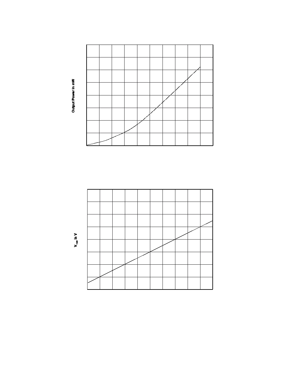
The trans mit ter RF out put power is pro por tional to the in put cur rent
to the TXMOD pin. A se ries re sis tor is used to ad just the peak trans -
mit ter out put power. 0 dBm out put power re quires about 250 µA of
in put cur rent.
Trans ceiver Mode Con trol
The four trans ceiver op er at ing modes ≠ re ceive, trans mit ASK,
trans mit OOK, and power-down (sleep), are con trolled by the Mod u -
la tion & Bias Con trol func tion, and are se lected with the CNTRL1
6

and CNTRL0 con trol pins. Set ting CNTRL1 and CNTRL0 both high
place the unit in the re ceive mode. Set ting CNTRL1 high and
CNTRL0 low place the unit in the ASK trans mit mode. Set ting
CNTRL1 low and CNTRL0 high place the unit in the OOK trans mit
mode. Set ting CNTRL1 and CNTRL0 both low place the unit in the
power-down (sleep) mode. Note that the re sis tor driv ing TXMOD
must be low in the re ceive and power-down modes. The PWIDTH
resistor must also be low in the power down mode to min i mize cur -
rent. CNTRL1 and CNTRL0 are CMOS com pat i ble in puts. These in -
puts must be held at a logic level; they can not be left un con nected.
Trans ceiver Event Tim ing
Trans ceiver event tim ing is sum ma rized in Ta ble 1. Please re fer to
this ta ble for the fol low ing dis cus sions.
Turn-On Tim ing
The max i mum time t
PR
re quired for the re ceive func tion to be come
op er a tional at turn on is in flu enced by two fac tors. All re ceiver cir -
cuitry will be op er a tional 5 ms af ter the sup ply volt age reaches
2.2 Vdc. The BBOUT-CMPIN cou pling-capacitor is then DC sta bi -
lized in 3 time con stants (3*t
BBC
). The to tal turn-on time to sta ble re -
ceiver op er a tion for a 10 ms power sup ply rise time is:
t
PR
= 15 ms + 3*t
BBC
The max i mum time re quired for ei ther the OOK or ASK trans mit ter
mode to be come op er a tional is 5 ms af ter the sup ply volt age
reaches 2.2 Vdc.
Re ceive-to-Transmit Tim ing
Af ter turn on, the max i mum time re quired to switch from re ceive to
ei ther trans mit mode is 12 µs. Most of this time is due to the start-up
of the trans mit ter os cil la tor.
Trans mit-to-Receive Tim ing
The max i mum time re quired to switch from the OOK or ASK trans -
mit mode to the re ceive mode is 3*t
BBC
, where t
BBC
is the BBOUT-
CMPIN cou pling-capacitor time con stant. When the op er at ing tem -
per a ture is lim ited to 60
o
C, the time re quired to switch from trans mit
to re ceive is dra mat i cally less for short trans mis sions, as less
charge leaks away from the BBOUT-CMPIN cou pling ca pac i tor.
Sleep and Wake-Up Tim ing
The max i mum tran si tion time from the re ceive mode to the
power-down (sleep) mode t
RS
is 10 µs af ter CNTRL1 and CNTRL0
are both low (1 µs fall time).
The max i mum tran si tion time from ei ther trans mit mode to the sleep
mode (t
TOS
and t
TAS
) is 10 µs af ter CNTRL1 and CNTRL0 are both
low (1 µs fall time).
The max i mum tran si tion time t
SR
from the sleep mode to the re ceive
mode is 3*t
BBC
, where t
BBC
is the BBOUT-CMPIN cou pling-capacitor
time con stant. When the op er at ing tem per a ture is lim ited to 60
o
C,
the time re quired to switch from sleep to re ceive is dra mat i cally less
for short sleep times, as less charge leaks away from the BBOUT-
CMPIN cou pling ca pac i tor.
The max i mum time re quired to switch from the sleep mode to ei ther
trans mit mode (t
STO
and t
STA
) is 16 µs. Most of this time is due to the
start-up of the trans mit ter os cil la tor.
AGC Tim ing
The max i mum AGC en gage time t
AGC
is 5 µs af ter the re cep tion of a
-30 dBm RF sig nal with a 1 µs en ve lope rise time.
The min i mum AGC hold-in time is set by the value of the ca pac i tor
at the AGCCAP pin. The hold-in time t
AGH
= C
AGC
/19.1, where t
AGH
is
in µs and C
AGC
is in pF.
Peak De tec tor Tim ing
The Peak De tec tor at tack time con stant is set by the value of the ca -
pac i tor at the PKDET pin. The at tack time t
PKA
= C
PKD
/4167, where
t
PKA
is in µs and C
PKD
is in pF. The Peak De tec tor de cay time con -
stant t
PKD
= 1000*t
PKA
.
Pulse Gen er a tor Tim ing
In the low data rate mode, the in ter val t
PRI
be tween the fall ing edge
of an ON pulse to the first RF am pli fier and the ris ing edge of the
next ON pulse to the first RF am pli fier is set by a re sis tor R
PR
be -
tween the PRATE pin and ground. The in ter val can be ad justed be -
tween 0.1 and 5 µs with a re sis tor in the range of 51 K to 2000 K.
The value of the R
PR
is given by:
R
PR
= 404* t
PRI
+ 10.5, where t
PRI
is in µs, and R
PR
is in kilohms
In the high data rate mode (se lected at the PWIDTH pin) the re -
ceiver RF am pli fi ers op er ate at a nom i nal 50%-50% duty cy cle. In
this case, the pe riod t
PRC
from the start of an ON pulse to the first
RF am pli fier to the start of the next ON pulse to the first RF am pli fier
is con trolled by the PRATE re sis tor over a range of 0.1 to 1.1 µs us -
ing a re sis tor of 11 K to 220 K. In this case R
PR
is given by:
R
PR
= 198* t
PRC
- 8.51, where t
PRC
is in µs and R
PR
is in kilohms
In the low data rate mode, the PWIDTH pin sets the width of the ON
pulse to the first RF am pli fier t
PW1
with a re sis tor R
PW
to ground (the
ON pulse width to the sec ond RF am pli fier t
PW2
is set at 1.1 times
the pulse width to the first RF am pli fier in the low data rate mode).
The ON pulse width t
PW1
can be ad justed be tween 0.55 and 1 µs
with a re sis tor value in the range of 200 K to 390 K. The value of
R
PW
is given by:
R
PW
= 404* t
PW1
- 18.6, where t
PW1
is in µs and R
PW
is in kilohms
How ever, when the PWIDTH pin is con nected to Vcc through a 1 M
re sis tor, the RF am pli fi ers op er ate at a nom i nal 50%-50% duty cy -
cle, fa cil i tat ing high data rate op er a tion. In this case, the RF am pli fi -
ers are con trolled by the PRATE re sis tor as de scribed above.
LPF Group De lay
The low-pass fil ter group de lay is a func tion of the fil ter 3 dB band -
width, which is set by a re sis tor R
LPF
to ground at the LPFADJ pin.
The min i mum 3 dB band width f
LPF
= 1445/R
LPF
, where f
LPF
is in kHz,
and R
LPF
is in kilohms.
The max i mum group de lay t
FGD
= 1750/f
LPF
= 1.21*R
LPF
, where t
FGD
is in µs, f
LPF
in kHz, and R
LPF
in kilohms.
7
Event
Symbol
Time
Min/Max
Test Conditions
Notes
Turn On to Re ceive
t
PR
3*t
BBC
+ 15 ms
max
10 ms supply voltage rise time
time until receiver operational
Turn On to TXOOK
t
PTO
15 ms
max
10 ms supply voltage rise time
time until TXMOD can modulate transmitter
Turn On to TXASK
t
PTA
15 ms
max
10 ms supply voltage rise time
time until TXMOD can modulate transmitter
RX to TXOOK
t
RTO
12 µs
max
1 µs CNTRL1 fall time
TXMOD low 1 µs before CNTRL1 falls
RX to TXASK
t
RTA
12 µs
max
1 µs CNTRL0 fall time
TXMOD low 1 µs before CNTRL0 falls
TXOOK to RX
t
TOR
3*t
BBC
max
1 µs CNTRL1 rise time
time until receiver operational
TXASK to RX
t
TAR
3*t
BBC
max
1 µs CNTRL0 rise time
time until receiver operational
Sleep to RX
t
SR
3*t
BBC
max
1µs CNTRL0/CNTROL1 rise times
time until receiver operational
Sleep to TXOOK
t
STO
16 µs
max
1 µs CNTRL0 rise time
time until TXMOD can modulate transmitter
Sleep to TXASK
t
STA
16 µs
max
1 µs CNTRL1 rise time
time until TXMOD can modulate transmitter
RX to Sleep
t
RS
10 µs
max
1µs CNTRL0/CNTROL1 fall times
time until transceiver is in power-down mode
TXOOK to Sleep
t
TOS
10 µs
max
1 µs CNTRL0 fall time
time until transceiver is in power-down mode
TXASK to Sleep
t
TAS
10 µs
max
1 µs CNTRL1 fall time
time until transceiver is in power-down mode
AGC En gage
t
AGC
5 µs
max
1 µs rise time, -30 dBm signal
RFA1 switches from 35 to 5 dB gain
AGC Hold-In
t
AGH
C
AGC/
19.1
min
CAGC in pF, t
AGH
in µs
user selected; longer than t
PKD
PKDET At tack Time Con stant
t
PKA
C
PKD
/4167
min
C
PKD
in pF, t
PKA
in µs
user selected
PKDET De cay Time Con stant
t
PKD
1000*t
PKA
min
t
PKD
and t
PKA
in µs
slaved to attack time
PRATE In ter val
t
PRI
0.1 to 5 µs
range
low data rate mode
user selected mode
PWIDTH RFA1
t
PW1
0.55 to 1 µs
range
low data rate mode
user selected mode
PWIDTH RFA2
t
PW2
1.1*t
PW1
range
low data rate mode
user selected mode
PRATE Cy cle
t
PRC
0.1 to 1.1 µs
range
high data rate mode
user selected mode
PWIDTH High (RFA1 & RFA2)
t
PWH
0.05 to 0.55 µs
range
high data rate mode
user selected mode
LPF Group De lay
t
FGD
1750/f
LPF
max
t
FGD
in µs, f
LPF
in kHz
user selected
LPF 3 dB Band width
f
LPF
1445/R
LPF
min
f
LPF
in kHz, R
LPF
in kilohms
user selected
BBOUT-CMPIN Time Con stant
t
BBC
0.064*C
BBO
min
t
BBC
in µs, C
BBO
in pF
user selected
Trans ceiver Event Tim ing, 3.0 Vdc, -40 to +85
0
C
Ta ble 1

Pin
Name
Description
1
GND1
GND1 is the RF ground pin. GND2 and GND3 should be connected to GND1 by short, low-inductance traces.
2
VCC1
VCC1 is the pos i tive sup ply volt age pin for the trans mit ter out put am pli fier and the re ceiver base-band cir cuitry.
VCC1 is usu ally con nected to the pos i tive sup ply through a fer rite RF de coup ling bead, which is by passed by an
RF ca pac i tor on the sup ply side. See the ASH Trans ceiver De signer's Guide for ad di tional in for ma tion.
3
AGCCAP
This pin con trols the AGC re set op er a tion. A ca pac i tor be tween this pin and ground sets the min i mum time the
AGC will hold-in once it is en gaged. The hold-in time is set to avoid AGC chat ter ing. For a given hold-in time t
AGH
,
the ca pac i tor value C
AGC
is:
C
AGC
= 19.1* t
AGH
, where t
AGH
is in µs and C
AGC
is in pF
A ±10% ce ramic ca pac i tor should be used at this pin. The value of C
AGC
given above pro vides a hold-in time be -
tween t
AGH
and 2.65* t
AGH
, de pend ing on op er at ing volt age, tem per a ture, etc. The hold-in time is cho sen to al low
the AGC to ride through the lon gest run of zero bits that can oc cur in a re ceived data stream. The AGC hold-in
time can be greater than the peak de tec tor de cay time, as dis cussed be low. How ever, the AGC hold-in time
should not be set too long, or the re ceiver will be slow in re turn ing to full sen si tiv ity once the AGC is en gaged by
noise or in ter fer ence. The use of AGC is op tional when us ing OOK mod u la tion with data pulses of at least 30 µs.
AGC op er a tion can be de feated by con nect ing this pin to Vcc. Ac tive or latched AGC op er a tion is re quired for
ASK mod u la tion and/or for data pulses of less than 30 µs. The AGC can be latched on once en gaged by con nect -
ing a 150 K re sis tor be tween this pin and ground, in stead of a ca pac i tor. AGC op er a tion de pends on a func tion ing
peak de tec tor, as dis cussed be low. The AGC ca pac i tor is dis charged in the re ceiver power-down (sleep) mode
and in the trans mit modes.
4
PKDET
This pin con trols the peak de tec tor op er a tion. A ca pac i tor be tween this pin and ground sets the peak de tec tor at -
tack and de cay times, which have a fixed 1:1000 ra tio. For most ap pli ca tions, these time con stants should be co -
or di nated with the base-band time con stant. For a given base-band ca pac i tor C
BBO
,
the ca pac i tor value C
PKD
is:
C
PKD
= 0.33* C
BBO
, where C
BBO
and C
PKD
are in pF
A ±10% ce ramic ca pac i tor should be used at this pin. This time con stant will vary be tween t
PKA
and 1.5* t
PKA
with
vari a tions in sup ply volt age, tem per a ture, etc. The ca pac i tor is driven from a 200 ohm "at tack" source, and de cays
through a 200 K load. The peak de tec tor is used to drive the "dB-below-peak" data slicer and the AGC re lease
func tion. The AGC hold-in time can be ex tended be yond the peak de tec tor de cay time with the AGC ca pac i tor, as
dis cussed above. Where low data rates and OOK mod u la tion are used, the "dB-below-peak" data slicer and the
AGC are op tional. In this case, the PKDET pin and the THLD2 pin can be left un con nected, and the AGC pin can
be con nected to Vcc to re duce the num ber of ex ter nal com po nents needed. The peak de tec tor ca pac i tor is dis -
charged in the re ceiver power-down (sleep) mode and in the trans mit modes.
5
BBOUT
BBOUT is the re ceiver base-band out put pin. This pin drives the CMPIN pin through a cou pling ca pac i tor C
BBO
for
in ter nal data slicer op er a tion. The time con stant t
BBC
for this con nec tion is:
t
BBC
= 0.064*C
BBO
, where t
BBC
is in µs and C
BBO
is in pF
A ±10% ce ramic ca pac i tor should be used be tween BBOUT and CMPIN. The time con stant can vary be tween t
BBC
and 1.8*t
BBC
with vari a tions in sup ply volt age, tem per a ture, etc. The op ti mum time con stant in a given cir cum -
stance will de pend on the data rate, data run length, and other fac tors as dis cussed in the ASH Trans ceiver De -
signer's Guide. A com mon cri te ria is to set the time con stant for no more than a 20% volt age droop dur ing SP
MAX
.
For this case:
C
BBO
= 70*SP
MAX
, where SP
MAX
is the max i mum sig nal pulse width in µs and C
BBO
is in pF
The out put from this pin can also be used to drive an ex ter nal data re cov ery pro cess (DSP, etc.). The nom i nal out -
put im ped ance of this pin is 1 K. When the re ceiver RF am pli fi ers are op er at ing at a 50%-50% duty cy cle, the
BBOUT sig nal changes about 10 mV/dB, with a peak-to-peak sig nal level of up to 685 mV. For lower duty cy cles,
the mV/dB slope and peak-to-peak sig nal level are pro por tion ately less. The sig nal at BBOUT is rid ing on a
1.1 Vdc value that var ies some what with sup ply volt age and tem per a ture, so it should be cou pled through a ca -
pac i tor to an ex ter nal load. A load im ped ance of 50 K to 500 K in par al lel with no more than 10 pF is rec om -
mended. When an ex ter nal data re cov ery pro cess is used with AGC, BBOUT must be cou pled to the ex ter nal
data re cov ery pro cess and CMPIN by sep a rate se ries cou pling ca pac i tors. The AGC re set func tion is driven by
the sig nal ap plied to CMPIN. When the trans ceiver is in power-down (sleep) or in a trans mit mode, the out put im -
ped ance of this pin be comes very high, pre serving the charge on the cou pling ca pac i tor.
6
CMPIN
This pin is the in put to the in ter nal data slic ers. It is driven from BBOUT through a cou pling ca pac i tor. The in put
im ped ance of this pin is 70 K to 100 K.
7
RXDATA
RXDATA is the re ceiver data out put pin. This pin will drive a 10 pF, 500 K par al lel load. The peak cur rent avail able
from this pin in creases with the re ceiver low-pass fil ter cut off fre quency. In the power-down (sleep) or trans mit
modes, this pin be comes high im ped ance. If re quired, a 1000 K pull-up or pull-down re sis tor can be used to es tab -
lish a def i nite logic state when this pin is high im ped ance. If a pull-up re sis tor is used, the pos i tive sup ply end
should be con nected to a volt age no greater than Vcc + 200 mV.
9
Pin De scrip tions

Pin
Name
Description
8
TXMOD
The trans mit ter RF out put volt age is pro por tional to the in put cur rent to this pin. A se ries re sis tor is used to ad just
the peak trans mit ter out put volt age. 0 dBm out put power re quires about 250 µA of in put cur rent. In the ASK mode,
min i mum out put power oc curs when the mod u la tion driver sinks about 10 µA of cur rent from this pin. In the OOK
mode, in put sig nals less than 220 mV com pletely turn the trans mit ter os cil la tor off. In ternally, this pin ap pears to
be a di ode in se ries with a small re sis tor. Peak trans mit ter out put power P
O
for a 3 Vdc sup ply volt age is ap prox i -
mately:
P
O
= 16*(I
TXM
)
2
, where P
O
is in mW, and the peak mod u la tion cur rent I
TXM
is in mA
A ±5% re sis tor value is rec om mended. In the OOK mode, this pin is usu ally driven with a logic-level data in put
(unshaped data pulses). OOK mod u la tion is prac ti cal for data pulses of 30 µs or lon ger. In the ASK mode, this pin
ac cepts an a log mod u la tion (shaped or unshaped data pulses). ASK mod u la tion is prac ti cal for data pulses 8.7 µs
or lon ger. The re sis tor driv ing this pin must be low in the re ceive and power-down (sleep) modes. Please re fer to
the ASH Trans ceiver De signer's Guide for ad di tional in for ma tion on mod u la tion tech niques.
9
LPFADJ
This pin is the re ceiver low-pass fil ter band width ad just. The fil ter band width is set by a re sis tor R
LPF
be tween this
pin and ground. The re sis tor value can range from 330 K to 820 ohms, pro vid ing a fil ter 3 dB band width f
LPF
from
4.5 kHz to 1.8 MHz. The re sis tor value is de ter mined by:
R
LPF
= 1445/ f
LPF
, where R
LPF
is in kilohms, and f
LPF
is in kHz
A ±5% re sis tor should be used to set the fil ter band width. This will pro vide a 3 dB fil ter band width be tween f
LPF
and 1.3* f
LPF
with vari a tions in sup ply volt age, tem per a ture, etc. The fil ter pro vides a three-pole, 0.05 de gree
equiripple phase re sponse. The peak drive cur rent avail able from RXDATA in creases in pro por tion to the fil ter
band width set ting.
10
GND2
GND2 is an IC ground pin. It should be connected to GND1 by a short, low in duc tance trace.
11
RREF
RREF is the ex ter nal ref er ence re sis tor pin. A 100 K ref er ence re sis tor is con nected be tween this pin and ground.
A ±1% re sis tor tol er ance is rec om mended. It is im por tant to keep the to tal ca pac i tance be tween ground, Vcc and
this node to less than 5 pF to main tain cur rent source sta bil ity. If THLD1 and/or THDL2 are con nected to RREF
through re sis tor val ues less that 1.5 K, their node ca pac i tance must be added to the RREF node ca pac i tance and
the to tal should not ex ceed 5 pF.
12
THLD2
THLD2 is the "dB-below-peak" data slicer (DS2) thresh old ad just pin. The thresh old is set by a 0 to 200 K re sis tor
R
TH2
be tween this pin and RREF. In creasing the value of the re sis tor de creases the thresh old be low the peak de -
tec tor value (in creases dif fer ence) from 0 to 120 mV. For most ap pli ca tions, this thresh old should be set at 6 dB
be low peak, or 60 mV for a 50%-50% RF am pli fier duty cy cle. The value of the THLD2 re sis tor is given by:
R
TH2
= 1.67*V, where R
TH2
is in kilohms and the thresh old V is in mV
A ±1% re sis tor tol er ance is rec om mended for the THLD2 re sis tor. Leaving the THLD2 pin open dis ables the
dB-below-peak data slicer op er a tion.
13
THLD1
The THLD1 pin sets the thresh old for the stan dard data slicer (DS1) through a re sis tor R
TH1
to RREF. The thresh -
old is in creased by in creas ing the re sis tor value. Con necting this pin di rectly to RREF pro vides zero thresh old.
The value of the re sis tor de pends on whether THLD2 is used. For the case that THLD2 is not used, the ac cept -
able range for the re sis tor is 0 to 100 K, pro vid ing a THLD1 range of 0 to 90 mV. The re sis tor value is given by:
R
TH1
= 1.11*V, where R
TH1
is in kilohms and the thresh old V is in mV
For the case that THLD2 is used, the ac cept able range for the THLD1 re sis tor is 0 to 200 K, again pro vid ing a
THLD1 range of 0 to 90 mV. The re sis tor value is given by:
R
TH1
= 2.22*V, where R
TH1
is in kilohms and the thresh old V is in mV
A ±1% re sis tor tol er ance is rec om mended for the THLD1 re sis tor. Note that a non-zero DS1 thresh old is re quired
for proper AGC op er a tion.
14
PRATE
The in ter val be tween the fall ing edge of an ON pulse to the first RF am pli fier and the ris ing edge of the next ON
pulse to the first RF am pli fier t
PRI
is set by a re sis tor R
PR
be tween this pin and ground. The in ter val t
PRI
can be ad -
justed be tween 0.1 and 5 µs with a re sis tor in the range of 51 K to 2000 K. The value of R
PR
is given by:
R
PR
= 404* t
PRI
+ 10.5, where t
PRI
is in µs, and R
PR
is in kilohms
A ±5% re sis tor value is rec om mended. When the PWIDTH pin is con nected to Vcc through a 1 M re sis tor, the RF
am pli fi ers op er ate at a nom i nal 50%-50% duty cy cle, fa cil i tat ing high data rate op er a tion. In this case, the pe riod
t
PRC
from start-to-start of ON pulses to the first RF am pli fier is con trolled by the PRATE re sis tor over a range of 0.1
to 1.1 µs us ing a re sis tor of 11 K to 220 K. In this case the value of R
PR
is given by:
R
PR
= 198* t
PRC
- 8.51, where t
PRC
is in µs and R
PR
is in kilohms
A ±5% re sis tor value should also be used in this case. Please re fer to the ASH Trans ceiver De signer's Guide for
ad di tional am pli fier duty cy cle in for ma tion. It is im por tant to keep the to tal ca pac i tance be tween ground, Vcc and
this pin to less than 5 pF to main tain sta bil ity.
10

Pin
Name
Description
15
PWIDTH
The PWIDTH pin sets the width of the ON pulse to the first RF am pli fier t
PW1
with a re sis tor R
PW
to ground (the ON
pulse width to the sec ond RF am pli fier t
PW2
is set at 1.1 times the pulse width to the first RF am pli fier). The ON
pulse width t
PW1
can be ad justed be tween 0.55 and 1 µs with a re sis tor value in the range of 200 K to 390 K. The
value of R
PW
is given by:
R
PW
= 404* t
PW1
- 18.6, where t
PW1
is in µs and R
PW
is in kilohms
A ±5% re sis tor value is rec om mended. When this pin is con nected to Vcc through a 1 M re sis tor, the RF am pli fi -
ers op er ate at a nom i nal 50%-50% duty cy cle, fa cil i tat ing high data rate op er a tion. In this case, the RF am pli fier
ON times are con trolled by the PRATE re sis tor as de scribed above. It is im por tant to keep the to tal ca pac i tance
be tween ground, Vcc and this node to less than 5 pF to main tain sta bil ity. When us ing the high data rate op er a tion
with the sleep mode, con nect the 1 M re sis tor be tween this pin and CNTRL1 (Pin 17), so this pin is low in the
sleep mode.
16
VCC2
VCC2 is the pos i tive sup ply volt age pin for the re ceiver RF sec tion and trans mit ter os cil la tor. Pin 16 must be by -
passed with an RF ca pac i tor, and must also be by passed with a 1 to 10 µF tan ta lum or elec tro lytic ca pac i tor. See
the ASH Trans ceiver De signer's Guide for ad di tional in for ma tion.
17
CNTRL1
CNTRL1 and CNTRL0 se lect the re ceive and trans mit modes. CNTRL1 and CNTRL0 both high place the unit in
the re ceive mode. CNTRL1 high and CNTRL0 low place the unit in the ASK trans mit mode. CNTRL1 low and
CNTRL0 high place the unit in the OOK trans mit mode. CNTRL1 and CNTRL0 both low place the unit in the
power-down (sleep) mode. CNTRL1 is a high-impedance in put (CMOS com pat i ble). An in put volt age of 0 to
300 mV is in ter preted as a logic low. An in put volt age of Vcc - 300 mV or greater is in ter preted as a logic high. An
in put volt age greater than Vcc + 200 mV should not be ap plied to this pin. A logic high re quires a max i mum
source cur rent of 40 µA. A logic low re quires a max i mum sink cur rent of 25 µA (1 µA in sleep mode). This pin
must be held at a logic level; it can not be left un con nected.
18
CNTRL0
CNTRL0 is used with CNTRL1 to con trol the re ceive and trans mit modes of the trans ceiver. CNTRL0 is a
high-impedance in put (CMOS com pat i ble). An in put volt age of 0 to 300 mV is in ter preted as a logic low. An in put
volt age of Vcc - 300 mV or greater is in ter preted as a logic high. An in put volt age greater than Vcc + 200 mV
should not be ap plied to this pin. A logic high re quires a max i mum source cur rent of 40 µA. A logic low re quires a
max i mum sink cur rent of 25 µA (1 µA in sleep mode). This pin must be held at a logic level; it can not be left un -
con nected.
19
GND3
GND3 is an IC ground pin. It should be con nected to GND1 by a short, low in duc tance trace.
20
RFIO
RFIO is the RF in put/out put pin. This pin is con nected di rectly to the SAW fil ter trans ducer. An tennas pre sent ing
an im ped ance in the range of 35 to 72 ohms re sis tive can be sat is fac to rily matched to this pin with a se ries match -
ing coil and a shunt match ing/ESD pro tec tion coil. Other an tenna im ped ances can be matched us ing two or three
com po nents. For some im ped ances, two inductors and a ca pac i tor will be re quired. A DC path from RFIO to
ground is required for ESD pro tec tion.
11
SM-20H PCB Pad Layout
Dimensions in inches.
.09
.370
0.000
.065
.105
.145
.185
.225
.265
.305
.345
.435
12
Note: Spec i fi ca tions sub ject to change with out no tice.
file: tr3005.vp, 121305 rev
0.20
0.40
0.60
0.80
1.00
1.20
1.40
1.60
3 V
RF Output Power vs I
TXM
I
TXM
in µA
25
50
75
100
125
150
175
200
275
250
225
I
TXM
in µA
V
TXM
vs I
TXM
0.85
0.90
0.95
1.00
1.05
1.10
1.15
1.20
25
50
75
100
125
150
175
200
275
250
225