!
2-33
2
PO
WER
AMPLI
F
I
E
RS
Product Description
Ordering Information
Typical Applications
Features
Functional Block Diagram
RF Micro Devices, Inc.
7625 Thorndike Road
Greensboro, NC 27409, USA
Tel (336) 664 1233
Fax (336) 664 0454
http://www.rfmd.com
Optimum Technology MatchingÆ Applied
Si BJT
GaAs MESFET
GaAs HBT
Si Bi-CMOS
SiGe HBT
Si CMOS
RF1 IN
GND
GND
PD
RF2 IN
RF1 OUT
VCC1
RF2 OUT
RF2 OUT
GND
GND
GND
RF2 OUT
RF2 OUT
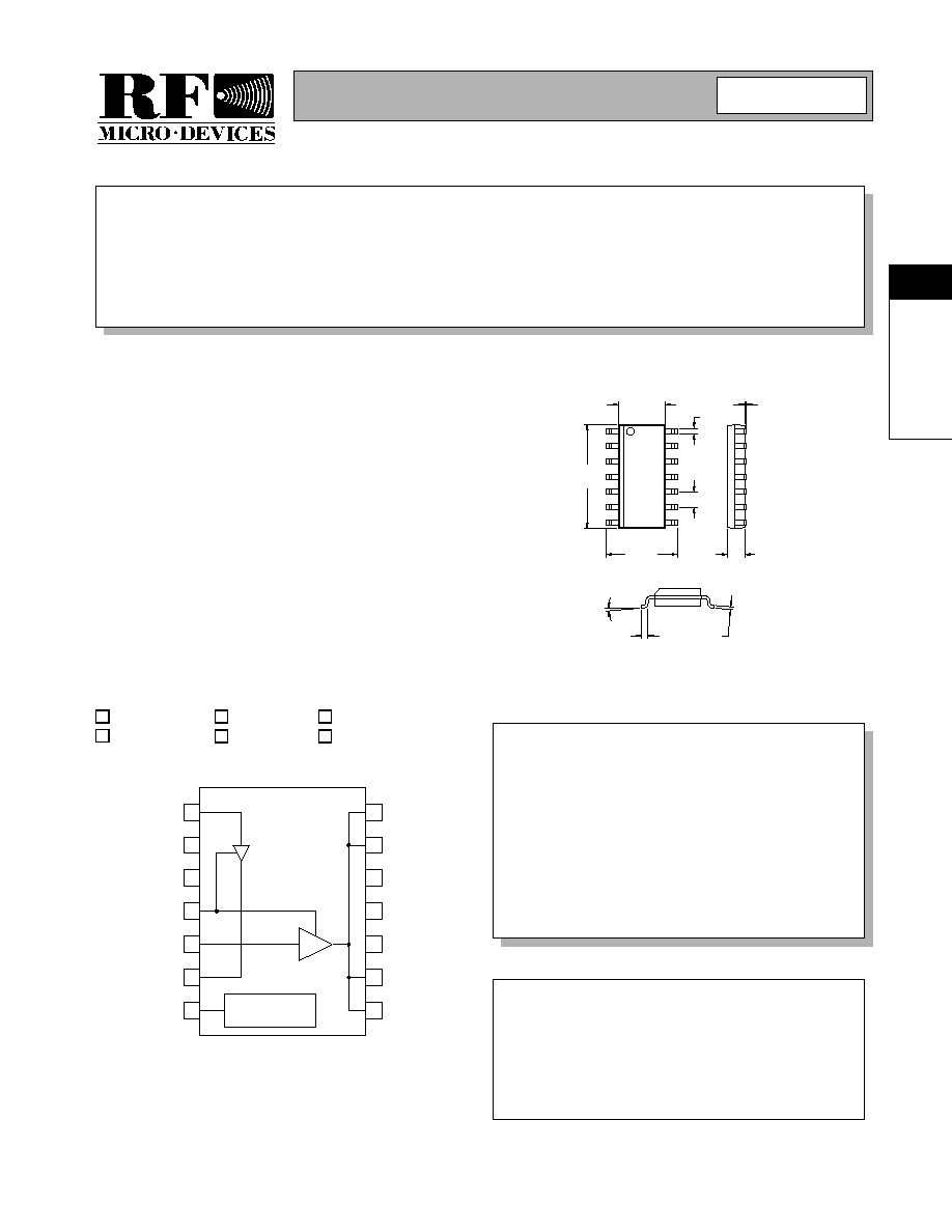
BIAS CIRCUIT
PA
PRE AMP
1
2
3
4
5
6
7
14
13
12
11
10
9
8
RF2114
MEDIUM POWER LINEAR AMPLIFIER
∑ Digital Communication Systems
∑ Spread-Spectrum Communication Systems
∑ Driver for Higher Power Linear Applications
∑ Portable Battery-Powered Equipment
∑ Commercial and Consumer Systems
∑ Base Station Equipment
The RF2114 is a medium to high power linear amplifier
IC. The device is manufactured on an advanced Gallium
Arsenide Heterojunction Bipolar Transistor (HBT) pro-
cess, and has been designed for use as the final linear
RF amplifier in UHF radio transmitters operating between
1 MHz and 600 MHz. It may also be used as a driver
amplifier in higher power applications. The device is self-
contained with the exception of the output matching net-
work, power supply feed line, and bypass capacitors. The
device can be used in 3-cell battery applications. The
maximum CW output at 3V is 125mW. The unit has a
total gain of 35dB, depending upon the output matching
network.
∑ 1MHz to 600MHz Operation
∑ Over 800mW CW Output Power
∑ 35dB Small Signal Gain
∑ Single 2.7V to 6.5V Supply
∑ 45% Efficiency
∑ Digitally Controlled Power Down Mode
RF2114
Medium Power Linear Amplifier
RF2114 PCBA
Fully Assembled Evaluation Board
2
Rev A5 001222
0.156
0.148
0.059
0.057
0.252
0.236
0.010
0.004
.018
.014
8∞ MAX
0∞ MIN
0.0500
0.0164
0.010
0.007
0.347
0.339
0.050
Package Style: SOIC-14
2-34
RF2114
Rev A5 001222
2
PO
WER
AMPLI
F
I
E
RS
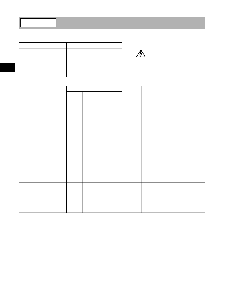
Absolute Maximum Ratings
Parameter
Rating
Unit
Supply Voltage
-0.5 to +8.5
V
DC
Power Down Voltage (V
PD
)
-0.5 to +5.0
V
DC Supply Current
500
mA
Input RF Power
+12
dBm
Output Load VSWR
20:1
Operating Ambient Temperature
-40 to +85
∞C
Storage Temperature
-40 to +150
∞C
Parameter
Specification
Unit
Condition
Min.
Typ.
Max.
Overall
T = 25∞C, V
CC
=5.8V, V
PD
=4.0 V,
Z
LOAD
= 18
, P
IN
= 6dBm, Freq= 150MHz
Frequency Range
1 to 600
MHz
Saturated Output Power
+28
+29
+31
dBm
Output Power
>+27
dBm
Frequency> 450MHz
Power Gain
30
36
40
dB
CW Total Efficiency
45
%
Two Tone Total Efficiency
26
%
P
OUT
= +19dBm/tone
IM
3
-50
-40
-25
dBc
P
OUT
= +19dBm/tone
IM
5
-70
-43
-30
dBc
P
OUT
= +19dBm/tone
Second Harmonic
-24
dBc
Without external second harmonic trap
Third Harmonic
-30
dBc
Output Noise Power
< -125
dBm/Hz
Input VSWR
<3:1
With external matching network; see appli-
cation schematic
Input Impedance
50
With external matching network; see appli-
cation schematic
Load Impedance
18+ j0
Load impedance for optimal match
Power Down Control
Power Down "ON"
V
CC
V
Voltage supplied to the input; Part is "ON"
Power Down "OFF"
0
0.2
V
Voltage supplied to the input; Part is "OFF"
Power Supply
Power Supply Voltage
2.7 to 6.5
V
Power Supply Idle Current
45
90
mA
Supply Current
150
300
500
mA
Total of pins 5 and 6
V
PD
Current
< 3.5
mA
Into pin 4
Total "OFF" Current Drain
10
µ
A
V
PD
< 0.1V
DC
Turn-on Time
< 100
ns
V
PD
= 0 to V
PD
=+4V
DC
Caution! ESD sensitive device.
RF Micro Devices believes the furnished information is correct and accurate
at the time of this printing. However, RF Micro Devices reserves the right to
make changes to its products without notice. RF Micro Devices does not
assume responsibility for the use of the described product(s).

2-35
RF2114
Rev A5 001222
2
PO
WER
AMPLI
F
I
E
RS
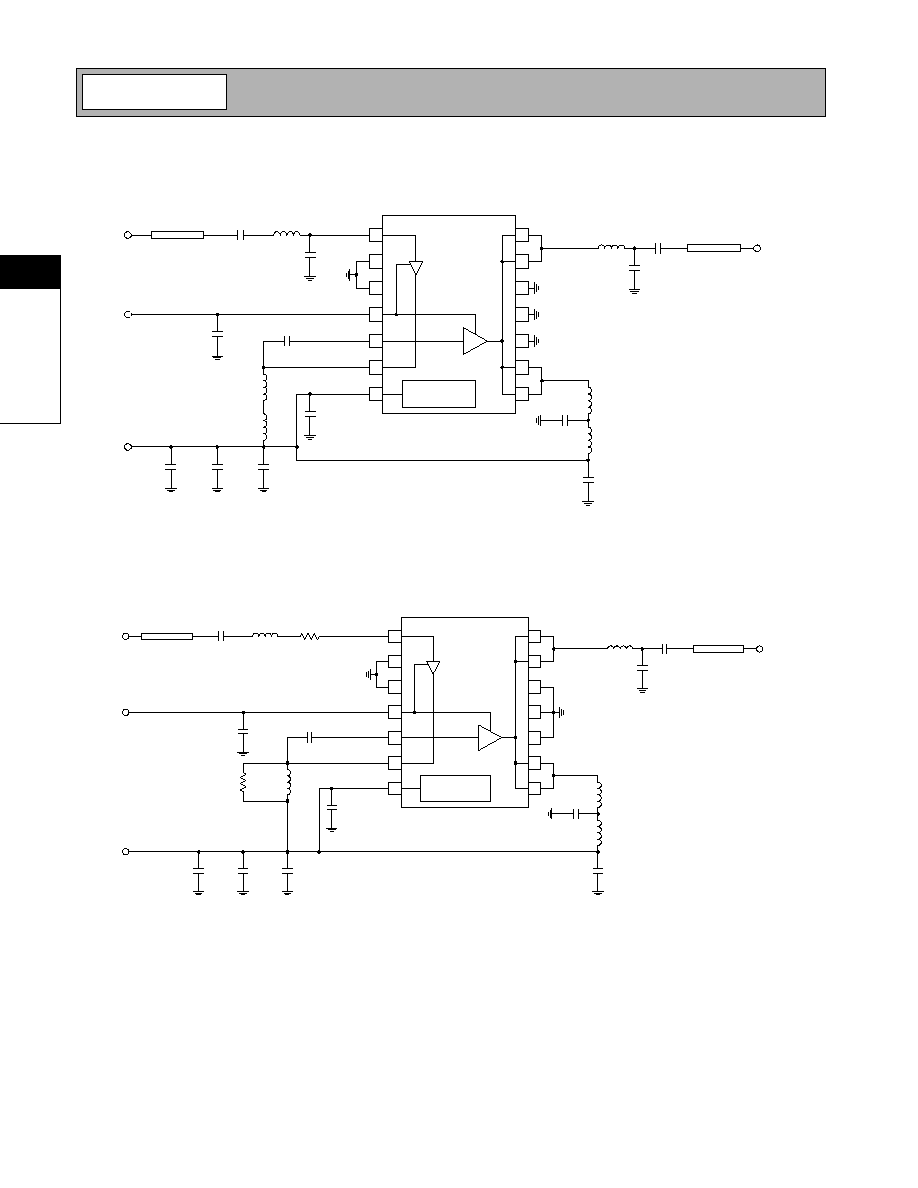
Pin
Function
Description
Interface Schematic
1
RF1 IN
RF input pin. This pin is internally connected to the bias circuits. An
external DC blocking capacitor is required. The value of this capacitor
depends on the actual operating frequency.
2
GND
Ground connection. Keep the connection to the backside ground plane
as short as possible, by placing the vias close to the pin.
3
GND
Same as pin 2.
4
PD
Power down control voltage. When this pin is at 0V, the device will be in
power down mode, dissipating minimum DC power. When this pin is at
V
CC
(but not higher than 5.0V max), the device will be in full power
mode delivering maximum gain and output power capability. This pin
may also be used to perform some degree of gain control or power con-
trol when set to voltages between 0V and V
CC
or 5.0V, whichever is the
lowest. It is not optimized for this function so the transfer function is not
linear over a wide range as with other devices specifically designed for
analog gain control. However, it may be usable for coarse adjustment or
in some closed loop AGC systems. This pin should not, in any circum-
stance, be higher in voltage than V
CC
. This pin should also have an
external bypassing capacitor.
5
RF2 IN
RF input of the power stage. This pin is internally connected to the bias
circuits. An external DC blocking capacitor is required. This same
capacitor can also be used for interstage matching. Typically this
capacitor is between RF2 IN (pin 5) and RF1 OUT (pin 6); see the
application schematics for details.
6
RF1 OUT
RF output of the pre-amplifier. Power supply needs to be supplied to
this pin through an inductor to V
CC
. Together with the series capacitor
between pin 5 and 6 the interstage matching circuit is formed. See the
application schematics for values for different frequencies.
7
VCC1
Positive supply for the active bias circuits. This needs to be bypassed
with a single capacitor, placed as close as possible to the package.
Additional bypassing of 1
µ
F is also recommended, but proximity to the
package is not as critical.
8
RF2 OUT
Amplifier RF output. This is an unmatched collector output of the final
amplifier transistor. Pins 8, 9, 13, and 14 are connected internally. Bias
for the final power amplifier output transistor must also be provided
through one of these two pins. Typically, pins 8 and 9 are connected to
a network that provides the DC bias and also creates a second har-
monic trap. A capacitor series resonates with internal bond wires and
some additional series inductance, and acts as a trap at two times the
operating frequency, effectively shorting out the second harmonic.
Shorting out this harmonic serves to increase the amplifier's maximum
output power and efficiency, as well as to lower the level of the second
harmonic output. Typically, pins 13 and 14 are externally connected
very close to the package and used as the RF output with a matching
network that presents the optimum load impedance to the PA for maxi-
mum power and efficiency, as well as providing DC blocking at the out-
put.
9
RF2 OUT
Same as pin 8.
10
GND
Same as pin 2.
11
GND
Same as pin 2.
12
GND
Same as pin 2.
13
RF2 OUT
Same as pin 8.
14
RF2 OUT
Same as pin 8.
2-36
RF2114
Rev A5 001222
2
PO
WER
AMPLI
F
I
E
RS
Application Schematic for 150MHz Operation
Application Schematic for 450MHz Operation
P1-1
P1-3
1
2
3
4
5
6
7
14
13
12
11
10
9
8
BIAS CIRCUIT
PA
PRE AMP
RF INPUT
50
µ
strip
100 nH
330 pF
330 pF
1200 nH
330 pF
10 nF
120 pF
10
µ
F
1 nF
22 nH
330 pF
50
µ
strip
RF OUTPUT
24 pF
5.6 nH
22 nH
33 pF
330 pF
6.8 pF
150 nH
P1-1
P1-3
1
2
3
4
5
6
7
14
13
12
11
10
9
8
BIAS CIRCUIT
PA
PRE
AMP
RF INPUT
Designed for V
CC
= 5 V
V
PC
= 5 V
P
OUT
= 500 mW
22
33 nH
20 pF
100 pF
12 nH
200
330 pF
10 nF
4.3 pF
10
µ
F
100 pF
6.8 nH
150 pF
50
µ
strip
RF OUTPUT
9.1 pF
1.8 nH
10 nH
4.3 pF
100 pF
50
µ
strip
2-37
RF2114
Rev A5 001222
2
PO
WER
AMPLI
F
I
E
RS
Evaluation Board Schematic (150MHz)
(Download Bill of Materials from www.rfmd.com.)
L2
22 nH
C5
330 pF
C4
24 pF
L6
5.6 nH
C9
33 pF
L5
22 nH
C8
330 pF
C10
1 nF
P1-1
C11
10
µ
F
C3
120 pF
L3
1200 nH
C7
330 pF
C2
6.8 pF
C6
1 nF
P1-3
1
2
3
4
5
6
7
14
13
12
11
10
9
8
BIAS CIRCUIT
PA
PRE
AMP
C1
330 pF
L4
150 nH
C12
10 nF
2114400 Rev A
136 MHz to 178 MHz
J2
RF OUT
J1
RF IN
L1
100 nH
50
µ
strip
50
µ
strip
P1-3
PC
GND
P1-1
VCC
P1
1
2
3