¸
2-39
2
PO
W
E
R
A
M
P
LI
FI
E
R
S
Product Description
Ordering Information
Typical Applications
Features
Functional Block Diagram
RF Micro Devices, Inc.
7625 Thorndike Road
Greensboro, NC 27409, USA
Tel (336) 664 1233
Fax (336) 664 0454
http://www.rfmd.com
Optimum Technology MatchingÆ Applied
Si BJT
GaAs MESFET
GaAs HBT
Si Bi-CMOS
SiGe HBT
Si CMOS
See
Upg
ra
ded
P
rod
uct
RF2
11
7
2
3
4
5
13
12
11
10
VCC3
VCC1
GND
PD
RF OUT
GND
RF OUT
RF OUT
6
7
8
9
1
14
15
16
RF
I
N
G20
G10
NC
VCC2
NC
NC
RF
O
U
T
BIAS
CIRCUIT
GAIN CONTROL
RF2115L
HIGH POWER UHF AMPLIFIER
∑ Analog Communication Systems
∑ Analog Cellular Systems (AMPS & TACS)
∑ 900MHz Spread-Spectrum Systems
∑ 400MHz Industrial Radios
∑ Driver Stage for Higher Power Applications
∑ Portable Battery-Powered Equipment
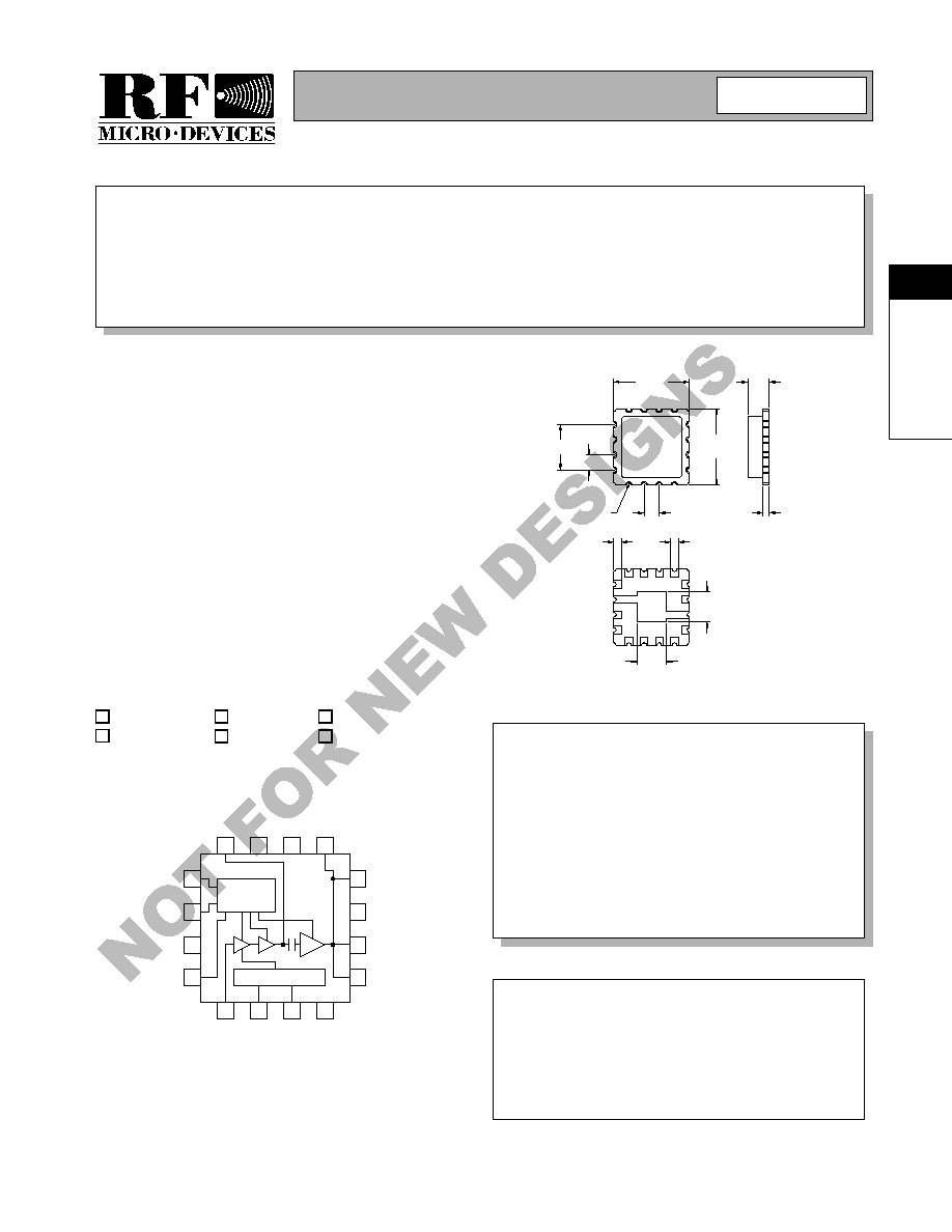
The RF2115L is a high power amplifier IC. The device is
manufactured on an advanced Gallium Arsenide Hetero-
junction Bipolar Transistor (HBT) process, and has been
designed for use as the final RF amplifier in analog cellu-
lar phone transmitters or ISM applications operating at
915MHz. The device is packaged in a 16-lead ceramic
quad leadless chip carrier with a backside ground. The
device is self-contained with the exception of the output
matching network and power supply feed line. A two-bit
digital control provides 4 levels of power control, in 10 dB
steps.
∑ Single 5V to 6.5V Supply
∑ Up to 1.0W CW Output Power
∑ 33dB Small Signal Gain
∑ 48% Efficiency
∑ Digitally Controlled Output Power
∑ Small Package Outline (0.25" x 0.25")
RF2115L
High Power UHF Amplifier
RF2115L PCBA
Fully Assembled Evaluation Board
2
Rev B1 010329
1
.258
.242
.258
.242
R.008
.022
.018
.025
.033
.017
.098
.098
.150
.050
.075
.065
.050
Package Style: QLCC-16

2-40
RF2115L
Rev B1 010329
2
PO
W
E
R
A
M
P
LI
FI
E
R
S
See
Upg
ra
ded
P
rod
uct
RF2
11
7
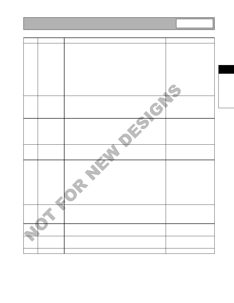
Absolute Maximum Ratings
Parameter
Rating
Unit
Supply Voltage (V
CC
)
-0.5 to +8.5
V
DC
Power Down Voltage (V
PD
)
-0.5 to +5.0
V
Control Voltage (G10, G20)
-0.5 to +5.5
V
DC Supply Current
700
mA
Input RF Power
+12
dBm
Output Load
20:1
Operating Case Temperature
-40 to +100
∞C
Operating Ambient Temperature
-40 to +85
∞C
Storage Temperature
-40 to +150
∞C
Parameter
Specification
Unit
Condition
Min.
Typ.
Max.
Overall
T = 25 ∞C, V
CC
= 5.8V, V
PD
= 5.0V, Z
LOAD
= 9
,
P
IN
=0dBm, Freq= 840MHz
Frequency Range
430 to 930
MHz
Maximum CW Output Power
+30.5
dBm
Note that increasing V
CC
does not result in
higher output power; power may actually
decrease.
+30
dBm
V
CC
= 5.8V, Z
LOAD
= 12
+29.5
dBm
V
CC
= 5.0V, Z
LOAD
= 9
+28.5
dBm
V
CC
= 5.0V, Z
LOAD
= 12
Total CW Efficiency at Maximum
Output
40
48
%
Small-signal Gain
33
dB
Second Harmonic
-23
dBc
Without external second harmonic trap
Third Harmonic
-36
dBc
Fourth Harmonic
-35
dBc
Input VSWR
<2:1
Input Impedance
50
Power Control
G20
G10
Output Power
+30
+30.5
+36
dBm
1
1
+17
+20
+23
dBm
1
0
+7
+11
+13
dBm
0
1
-4
+2.5
+6
dBm
0
0
Power Supply Current
350
415
600
mA
1
1
75
125
175
mA
1
0
35
56
90
mA
0
1
21
38
50
mA
0
0
Idle Current
30
55
80
mA
1
1
Power Down "ON"
5.0
V
Voltage supplied to the input; Part is "ON"
Power Down "OFF"
0
0.2
V
Voltage supplied to the input; Part is "OFF"
Power Down Control
Power Down "ON"
5.0
V
Voltage supplied to the input; Part is "ON"
Power Down "OFF"
0
0.2
V
Voltage supplied to the input; Part is "OFF"
Current Drain
1
10
µ
A
V
PD
< 0.1 V
DC
Caution! ESD sensitive device.
RF Micro Devices believes the furnished information is correct and accurate
at the time of this printing. However, RF Micro Devices reserves the right to
make changes to its products without notice. RF Micro Devices does not
assume responsibility for the use of the described product(s).
2-41
RF2115L
Rev B1 010329
2
PO
W
E
R
A
M
P
LI
FI
E
R
S
See
Upg
ra
ded
P
rod
uct
RF2
11
7
Pin
Function
Description
Interface Schematic
1
VCC2
Positive supply for the second stage (driver) amplifier. This is an
unmatched transistor collector output. This pin should see an inductive
path to AC ground (V
CC
with a UHF bypassing capacitor). This induc-
tance can be achieved with a short, thin microstrip line or with a low
value chip inductor (approximately 2.7nH). At lower frequencies, the
inductance value should be larger (longer microstrip line) and V
CC
should be bypassed with a larger bypass capacitor (see the application
schematic for 430MHz operation). This inductance forms a matching
network with the internal series capacitor between the second and third
stages, setting the amplifier's frequency of maximum gain. An addi-
tional 1
µ
F bypass capacitor in parallel with the UHF bypass capacitor is
also recommended, but placement of this component is not as critical.
In most applications, pins 1, 2, and 3 can share a single 1
µ
F bypass
capacitor.
2
VCC3
Positive supply for the active bias circuits. This pin can be externally
combined with pin 3 (VCC1) and the pair bypassed with a single UHF
capacitor, placed as close as possible to the package. Additional
bypassing of 1
µ
F is also recommended, but proximity to the package is
not as critical. In most applications, pins 1, 2, and 3 can share a single
1
µ
F bypass capacitor.
3
VCC1
Positive supply for the first stage (input) amplifier. This pin can be exter-
nally combined with pin 2 (VCC3) and the pair bypassed with a single
UHF capacitor, placed as close as possible to the package. Additional
bypassing of 1
µ
F is also recommended, but proximity to the package is
not as critical. In most applications, pins 1, 2, and 3 can share a single
1
µ
F bypass capacitor. This pin can also be used for coarse analog gain
control, even though it is not optimized for this function.
4
GND
Ground connection. Keep traces physically short and connect immedi-
ately to ground plane for best performance. In addition, for specified
performance, the package's backside metal should be soldered to
ground plane.
5
PD
Power down control voltage. When this pin is at 0V, the device will be in
power down mode, dissipating minimum DC power. When this pin is at
5V the device will be in full power mode delivering maximum available
gain and output power capability. This pin may also be used to perform
some degree of gain control or power control when set to voltages
between 0V and 5V. It is not optimized for this function so the transfer
function is not linear over a wide range as with other devices specifi-
cally designed for analog gain control; however, it may be usable for
coarse adjustment or in some closed loop AGC systems. This pin
should not, in any circumstance, be higher in voltage than V
CC
, nor
should it ever be higher than 6.5V. This pin should also have an exter-
nal UHF bypassing capacitor.
6
RF IN
Amplifier RF input. This is a 50
RF input port to the amplifier. It does
not contain internal DC blocking and therefore should be externally DC
blocked before connecting to any device which has DC present or
which contains a DC path to ground. A series UHF capacitor is recom-
mended for the DC blocking.
7
G20
RF output power gain control MSB (see specification table for logic).
The control voltage at this pin should never exceed V
CC
. This pin
should also have an external UHF bypassing capacitor.
8
G10
RF output power gain control LSB (see specification table for logic).
The control voltage at this pin should never exceed V
CC
. This pin
should also have an external UHF bypassing capacitor.
9
NC
Not internally connected.

2-42
RF2115L
Rev B1 010329
2
PO
W
E
R
A
M
P
LI
FI
E
R
S
See
Upg
ra
ded
P
rod
uct
RF2
11
7
Pin
Function
Description
Interface Schematic
10
RF OUT
Amplifier RF output. This is an unmatched collector output of the final
amplifier transistor. It is internally connected to pins 10, 11, 13, and 14
to provide low series inductance and flexibility in output matching. Bias
for the final power amplifier output transistor must also be provided
through two of these four pins. Typically, pins 10 and 11 are connected
to a network that creates a second harmonic trap. For 830MHz opera-
tion, this network is simply a single 2.4pF capacitor from both pins to
ground. This capacitor series resonates with internal bond wires at two
times the operating frequency, effectively shorting out the second har-
monic. Shorting out this harmonic serves to increase the amplifier's
maximum output power and efficiency, as well as to lower the level of
the second harmonic output. Typically, pins 13 and 14 are externally
connected very close to the package and used as the RF output with a
matching network that presents the optimum load impedance to the PA
for maximum power and efficiency, as well as providing DC blocking at
the output. An additional network of a bias inductor and parallel resistor
provides DC bias and helps to protect the output from high voltage
swings due to severe load mismatches. Shunt protection diodes are
included to clip peak voltage excursions above approximately 15V to
prevent voltage breakdown in worst case conditions.
11
RF OUT
Same as pin 10.
12
GND
Same as pin 4.
13
RF OUT
Same as pin 10.
14
RF OUT
Same as pin 10.
15
NC
Not internally connected.
16
NC
Not internally connected.
Pkg
Base
GND
This contact is the main ground contact for the entire device. Care
should be taken to ensure that this contact is well soldered in order to
prevent performance from being degraded from that indicated in the
specifications.
