¸
2-61
2
PO
W
E
R
A
M
P
LI
FI
E
R
S
Product Description
Ordering Information
Typical Applications
Features
Functional Block Diagram
RF Micro Devices, Inc.
7625 Thorndike Road
Greensboro, NC 27409, USA
Tel (336) 664 1233
Fax (336) 664 0454
http://www.rfmd.com
Optimum Technology MatchingÆ Applied
Si BJT
GaAs MESFET
GaAs HBT
Si Bi-CMOS
SiGe HBT
Si CMOS
See
Upg
ra
ded
P
rod
uct
RF2
12
5P
1
2
3
4
8
7
6
5
RF IN
RF IN
PC
VCC
RF OUT
RF OUT
RF OUT
RF OUT
BIAS
CIRCUIT
PACKAGE BASE
GND
RF2125
HIGH POWER LINEAR AMPLIFIER
∑ PCS Communication Systems
∑ Digital Communication Systems
∑ DECT Cordless Applications
∑ Commercial and Consumer Systems
∑ Portable Battery Powered Equipment
The RF2125 is a high power, high efficiency linear ampli-
fier IC. The device is manufactured on an advanced Gal-
lium Arsenide Heterojunction Bipolar Transistor (HBT)
process, and has been designed for use as the final RF
amplifier in digital PCS phone transmitters and base sta-
tions requiring linear amplification operating between
1500 MHz and 2200 MHz. It will also function as a high
efficiency amplifier for constant envelope applications
such as DECT. The device is packaged in an 8-lead
ceramic package with a backside ground. The device is
self-contained with the exception of the output matching
network and power supply feed line. It produces a typical
output power level of 1 W.
∑ Single 2.7V to 7.5V Supply
∑ 1W Output Power
∑ 14dB Gain
∑ 45% Efficiency
∑ Power Down Mode
∑ 1500MHz to 2200MHz Operation
RF2125
High Power Linear Amplifier
RF2125 PCBA
Fully Assembled Evaluation Board
2
Rev A7 010112
.315
.305
.180 SQ MAX
.017
.013
.050
.006
.004
4∞MAX
0∞MIN
.017
.013
.057 MAX
.004
.000
1
.166
SQ
Metal lid and base, gold plated
Package Style: SOP-8-C

2-62
RF2125
Rev A7 010112
2
PO
W
E
R
A
M
P
LI
FI
E
R
S
See
Upg
ra
ded
P
rod
uct
RF2
12
5P
Absolute Maximum Ratings
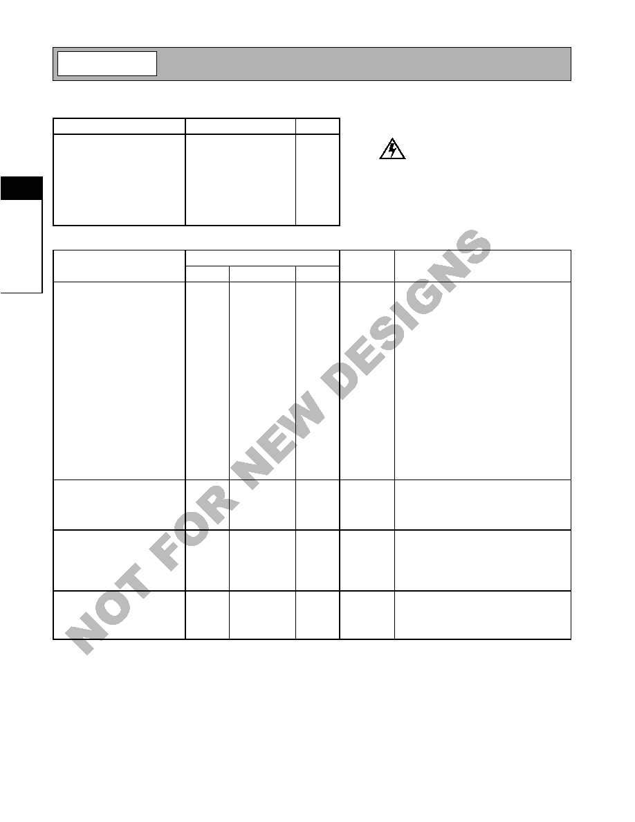
Parameter
Rating
Unit
Supply Voltage (V
CC
)
-0.5 to +7.5
V
DC
Power Control Voltage (V
PC
)
-0.5 to +3.6V
V
DC Supply Current
450
mA
Input RF Power
+20
dBm
Output Load
20:1
Operating Case Temperature
-40 to +100
∞C
Operating Ambient Temperature
-40 to +85
∞C
Storage Temperature
-40 to +150
∞C
Parameter
Specification
Unit
Condition
Min.
Typ.
Max.
Overall
T = 25 ∞C, V
CC
=6.0V, V
PC
= 3.5V,
Z
LOAD
= 12
, P
IN
= 0dBm, Freq= 1885MHz,
Idle current=180mA
Frequency Range
1500 to 2200
MHz
Maximum Output Power
+28.5
dBm
V
CC
= 3.6V, P
IN
= +17dBm
Maximum Output Power
+29.5
dBm
V
CC
= 4.8V, P
IN
= +17dBm
Maximum Output Power
+29.3
+30
dBm
V
CC
= 6.0V, P
IN
= +17dBm
Total Power Added Efficiency
45
%
Maximum output, V
CC
= 3.6V
Total Power Added Efficiency
45
%
Maximum output, V
CC
= 4.8V
Total Power Added Efficiency
42
45
%
Maximum output, V
CC
= 6.0V
Small-signal Gain
12
14
dB
Second Harmonic
-40
dBc
Third Harmonic
-45
dBc
Fourth Harmonic
-35
dBc
Isolation
15
dB
V
PC
= 0.2V
Input VSWR
1.5:1
With external matching network; see appli-
cation schematic
Two-tone Specification
IM
3
-25
-30
dBc
P
OUT
=+23.5dBm for each tone
IM
5
-35
dBc
P
OUT
=+24dBm for each tone
IM
7
-45
dBc
P
OUT
=+24dBm for each tone
Power Control
V
PC
1.5
3.3
3.5
V
To obtain 180mA idle current
PC Current
1
mA
V
PC
= 2.0V
2
mA
V
PC
= 3.5V
Power Control "OFF"
0.2
0.5
V
Threshold voltage at device input
Power Supply
Power Supply voltage
2.7 to 7.5
V
Supply Current
270
360
440
mA
P
OUT
= +30dBm, V
CC
= 6.0V
Power Down Current
0.5
10
µ
A
V
PC
= 0.2V
Caution! ESD sensitive device.
RF Micro Devices believes the furnished information is correct and accurate
at the time of this printing. However, RF Micro Devices reserves the right to
make changes to its products without notice. RF Micro Devices does not
assume responsibility for the use of the described product(s).

2-63
RF2125
Rev A7 010112
2
PO
W
E
R
A
M
P
LI
FI
E
R
S
See
Upg
ra
ded
P
rod
uct
RF2
12
5P
Application Schematic
1880MHz
Pin
Function
Description
Interface Schematic
1
RF IN
RF input. This input is DC coupled, so an external blocking capacitor is
required if this pin is connected to a DC path. An optimum match to
50
is obtained by providing an external series capacitor of 4.3pF and
then a shunt capacitor of 3.3pF; see the application schematic. Those
values are typical for 1880MHz; other values may be required for other
frequencies.
2
RF IN
Same as pin 1.
3
PC
Power control pin. For obtaining maximum performance the voltage on
this pin can be used to set correct bias level. In a typical application this
is implemented by a feedback loop. The feedback can be based on the
actual supply current of the device, i.e., maintaining a fixed current
level, or it can be based on the RF output power level to maintain a
fixed RF power level (Automatic Level Control loop). A voltage of 0.5V
or lower brings the part into power down state.
4
VCC
Power supply pin for the bias circuits. External low frequency bypass
capacitors should be connected if no other low frequency decoupling is
nearby.
5
RF OUT
RF output and bias for the output stage. The power supply for the out-
put transistor needs to be supplied to this pin. This can be done
through a quarter wave length microstrip line that is RF grounded at the
other end, or through an RF inductor that supports the required DC cur-
rents. Optimum load impedance is achieved by providing a shunt
capacitor of 3.0pF and a series capacitor of 3.9pF; see the application
schematic. Those values are typical for 1880MHz; other values may be
required for other frequencies. Since there are several output pins
available, which are internally connected, one pin can be used for con-
necting the bias, another for connecting a (third) harmonic trap filter,
and the other pins for the RF output.
6
RF OUT
Same as pin 5.
7
RF OUT
Same as pin 5.
8
RF OUT
Same as pin 5.
Pkg
Base
GND
Ground connection. The backside of the package should be connected
to the ground plane through a short path, i.e., vias under the device
may be required.
1
2
3
4
8
7
6
5
BIAS
CIRCUIT
PACKAGE BASE
33 nH
3.3 pF
100 nF
3.9 pF
100 pF
100 nF
3.3 pF
RF IN
RF OUT
5.1 pF
V
CC
V
PD

2-64
RF2125
Rev A7 010112
2
PO
W
E
R
A
M
P
LI
FI
E
R
S
See
Upg
ra
ded
P
rod
uct
RF2
12
5P
Evaluation Board Schematic
1880MHz
(Download Bill of Materials from www.rfmd.com.)
Evaluation Board Layout
1.5" x 1.0"
Board Thickness 0.031"; Board Material FR-4
1
2
3
4
8
7
6
5
BIAS
CIRCUIT
PACKAGE BASE
L1
33 nH
C3
3.3 pF
C7
1 nF
C4
3.9 pF
C6
100 pF
C5
1
µ
F
C1
3.3 pF
P1-3
P1-1
C2
5.1 pF
C8
1 nF
C9
100 nF
RF OUT
RF IN
J1
J2
P1-1
P1-3
P1
PC
GND
VCC
1
2
3
2125401 Rev A
PTI Package
50
µ
strip
50
µ
strip

2-65
RF2125
Rev A7 010112
2
PO
W
E
R
A
M
P
LI
FI
E
R
S
See
Upg
ra
ded
P
rod
uct
RF2
12
5P
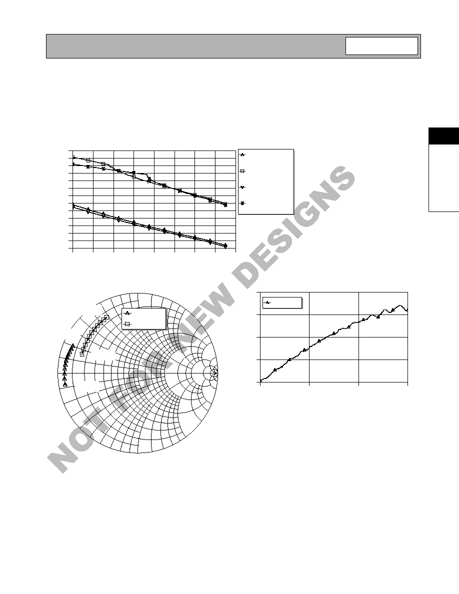
The data below is valid only under small-signal conditions. The device needs to be biased in Class A, with the out-
put power below the 1-dB compression point. For large signal operation this data may be used as a starting point,
but further tuning to optimize performance will be required.
Voltage and idle current have only very limited effect on the input and output impedances, hence only one plot is
shown, valid for V
CC
=5 to 7 V, and I
CC
= 50 to 250mA.
1
1.2
1.4
1.6
1.8
2
2.2
2.4
2.6
Frequency (GHz)
RF2125 Gain
0
2
4
6
8
10
12
14
16
18
20
22
24
26
Gai
n
(
d
B)
DB(|S[2,1]|)
Vcc=6.5V, Icc=200mA
DB(GMax)
Vcc=6.5V, Icc=200mA
DB(|S[2,1]|)
Vcc=5.0V, Icc=50mA
DB(GMax)
Vcc=5.0V, Icc=50mA
1
1.5
2
2.5
FREQUENCY (GHz)
RF2125 S12
-37
-36
-35
-34
-33
S1
2
(
d
B
)
DB(|S[1,2]|)
0
1.0
1.0
-1.0
10.0
10.0
-1
0.0
5.0
5.0
-5
.0
2.0
2.
0
-2
.0
3.0
3.
0
-3
.0
4.0
4.0
-4
.0
0.2
0.2
-0.2
0.4
0.
4
-0
.4
0.6
0
.6
-0
.6
0.8
0
.8
-0
.8
RF2125 Input / Output Impedance, Class A bias
Swp Max
2.5GHz
Swp Min
1GHz
S11
S22
1 GHz
1 GHz
2.5 GHz
2.5 GHz


