
¸
2-129
2
PO
W
E
R
A
M
P
LI
FI
E
R
S
Product Description
Ordering Information
Typical Applications
Features
Functional Block Diagram
RF Micro Devices, Inc.
7628 Thorndike Road
Greensboro, NC 27409, USA
Tel (336) 664 1233
Fax (336) 664 0454
http://www.rfmd.com
Optimum Technology MatchingÆ Applied
Si BJT
GaAs MESFET
GaAs HBT
Si Bi-CMOS
SiGe HBT
Si CMOS
Se
e
Up
gr
ade
d Pr
oduc
t RF21
74
1
2
3
4
5
13
12
11
10
9
AT_EN
RF IN
GND1
RF OUT
RF OUT
RF OUT
6
7
8
16
14
15
V
CC1
APC
1
APC
2
VC
C
NC
G
ND2
VC
C
2
VC
C
2
VC
C
2
2F0
RF2140
3V DCS POWER AMPLIFIER
∑ 3V DCS1800 (PCN) Cellular Handsets
∑ 3V DCS1900 (PCS) Cellular Handsets
∑ 3V Dual-Band/Triple-Band Handsets
∑ Commercial and Consumer Systems
∑ Portable Battery-Powered Equipment
∑ GPRS Compatible
The RF2140 is a high power, high efficiency power ampli-
fier module offering high performance in GSM or GPRS
applications. The device is manufactured on an advanced
GaAs HBT process, and has been designed for use as
the final RF amplifier in DCS1800/1900 hand held-digital
cellular
equipment
and
other
applications
in
the
1700 MHz to 2000MHz band. On-board power control
provides over 65dB of control range with an analog volt-
age input, and provides power down with a logic "low" for
standby operation. The device is self-contained with 50
input and the output can be easily matched to obtain opti-
mum power and efficiency characteristics.The RF2140
can be used together with the RF2138 for dual-band
operation. The device is packaged in an ultra-small
ceramic package, minimizing the required board space.
∑ Single 2.7V to 4.8V Supply Voltage
∑ +33dBm Output Power at 3.5V
∑ 27dB Gain with Analog Gain Control
∑ 51% Efficiency
∑ 1700MHz to 1950MHz Operation
∑ Supports DCS1800 and PCS1900
RF2140
3V DCS Power Amplifier
RF2140 PCBA
Fully Assembled Evaluation Board
2
Rev A12 011031
ALL SOLDER PAD TOLERANCES P0.05mm
1
4.20
3.95
sq.
3.50
3.35
sq.
0.38
1.50
1.20
2.00
0.28
0.13
0.80
1.50
sq.
0.40
sq.
Package Style: MP16K01A

2-130
RF2140
Rev A12 011031
2
PO
W
E
R
A
M
P
LI
FI
E
R
S
See
Upg
ra
ded
P
rod
uct
RF2
17
4
Absolute Maximum Ratings
Parameter
Rating
Unit
Supply Voltage
-0.5 to +6.0
V
DC
Power Control Voltage (V
APC
)
-0.5 to +3.0
V
Enable Voltage (V
AT_EN
)
-0.5 to +3.0
V
DC Supply Current
1500
mA
Input RF Power
+13
dBm
Duty Cycle at Max Power
50
%
Output Load VSWR
10:1
Operating Case Temperature
-40 to +85
∞C
Storage Temperature
-55 to +150
∞C
Parameter
Specification
Unit
Condition
Min.
Typ.
Max.
Overall
Temp= 25 ∞C, V
CC
= 3.5V, V
APC1,2
=2.6V,
V
AT_EN
=2.6V, P
IN
= +6dBm, Freq= 1710MHz
to 1910MHz, 25% Duty Cycle, pulse
width= 1154
µ
s
Operating Frequency Range
1710 to 1785
MHz
See application schematic for tuning details.
1850 to 1910
MHz
A different tuning is required.
Usable Frequency Range
1700 to 2000
MHz
Maximum Output Power
+32
+33
dBm
Temp= 25 ∞C, V
CC
= 3.5V, V
APC1,2
=2.6V
+31.5
+32.8
dBm
Temp= +25 ∞C, V
CC
= 3.2V, V
APC1,2
= 2.6V
+31.5
dBm
Temp= +85 ∞C, V
CC
= 3.2V, V
APC1,2
= 2.6V
+31
dBm
Temp= 25 ∞C, V
CC
= 2.7V, V
APC1,2
=2.6V
+29.5
+30
dBm
Temp= +85 ∞C, V
CC
= 2.7V, V
APC1,2
= 2.6V
Total Efficiency
45
51
%
At P
OUT,MAX
, V
CC
= 3.5V
51
%
At P
OUT,MAX
, V
CC
= 3.0V
15
%
P
OUT
= +20dBm
10
%
P
OUT
= +10dBm
Recommended Input Power
Range
+5
+7
+9
dBm
Output Noise Power
-79
dBm
RBW= 100kHz, 1805MHz to 1880MHz and
1930MHz to 1990MHz,
P
OUT,MIN
< P
OUT
< P
OUT,MAX
,
P
IN,MIN
< P
IN
< P
IN,MAX
, V
CC
= 3.0V to 5.0V
Forward Isolation
-37
-30
dBm
V
APC1,2
= 0.2V, P
IN
= +10dBm
-40
-35
dBm
V
APC1,2
= 0.2V, P
IN
=+6dBm
Second Harmonic
-60
-45
dBc
Third Harmonic
-65
-50
dBc
Fourth Harmonic
-50
-45
dBc
Fifth Harmonic
-50
-45
dBc
Sixth Harmonic
-50
-45
dBc
All Other Non-Harmonic Spuri-
ous
-36
dBm
Input Impedance
50
Input VSWR
2.2:1
P
OUT,MAX
-5dB <P
OUT
< P
OUT,MAX
3:1
P
OUT
< P
OUT,MAX
-5dB
Output Load VSWR
10:1
Spurious<-36dBm, V
APC1,2
= 0.2V to 2.6V,
RBW= 100kHz
Output Load Impedance
4.5-j3.9
Load Impedance presented at RF OUT pin
Caution! ESD sensitive device.
RF Micro Devices believes the furnished information is correct and accurate
at the time of this printing. However, RF Micro Devices reserves the right to
make changes to its products without notice. RF Micro Devices does not
assume responsibility for the use of the described product(s).

2-131
RF2140
Rev A12 011031
2
PO
W
E
R
A
M
P
LI
FI
E
R
S
See
Upg
ra
ded
P
rod
uct
RF2
17
4
Parameter
Specification
Unit
Condition
Min.
Typ.
Max.
Power Control
Power Control "ON"
2.6
V
Maximum P
OUT
, Voltage supplied to the
input
Power Control "OFF"
0.2
0.5
V
Minimum P
OUT
, Voltage supplied to the input
Attenuator Enable "ON"
2.5
2.6
2.85
V
For maximum isolation when V
APC
is low
Attenuator Enable "OFF"
0.2
0.5
V
For power down mode
Power Control Range
62
68
dB
V
APC1,2
= 0.2V to 2.6V, V
AT_EN
= 2.6V,
P
IN
= +10dBm
Gain Control Slope
100
dB/V
P
OUT
=-10dBm to +33dBm
APC Input Capacitance
10
pF
DC to 2MHz
APC Input Current
4.5
5
mA
V
APC1,2
= 2.6V
10
µ
A
V
APC1,2
=0V
AT_EN Input Current
500
µ
A
V
AT_EN
= 2.6V, V
APC1,2
=0V
10
µ
A
V
AT_EN
=0V, V
APC1,2
=0V
Turn On/Off Time
100
ns
Power Supply
Power Supply Voltage
3.5
V
Specifications
2.7
4.8
V
Nominal operating limits, P
OUT
< +33dBm
5.5
V
With maximum output load VSWR 6:1,
P
OUT
< +33dBm
Power Supply Current
1.3
A
DC Current at P
OUT,MAX
55
295
mA
Idle Current, P
IN
< -30dBm
1
10
µ
A
P
IN
< -30dBm, V
APC1,2
= 0.2V
1
10
µ
A
P
IN
< -30dBm, V
APC1,2
= 0.2V, Temp= +85 ∞C

2-132
RF2140
Rev A12 011031
2
PO
W
E
R
A
M
P
LI
FI
E
R
S
See
Upg
ra
ded
P
rod
uct
RF2
17
4
Pin
Function
Description
Interface Schematic
1
GND2
Ground connection for the driver stage. Keep traces physically short
and connect immediately to the ground plane for best performance. It is
important for stability that this pin has it's own vias to the groundplane,
to minimize any common inductance. This pin is internally connected to
the ground slug.
See pin 15.
2
AT_EN
Control input for the PIN diode. The purpose of the PIN diode is to
attenuate the RF input drive level when the V
APC
is low. This serves
both to reduce the leakage through the device cause by self biasing
when driving with high level at the RF input, as well as to maintain a
good input match when the bias of the input stage is turned off. When
this pin is "high" the PIN diode control is turned on. See the Theory of
Operation for more details.
3
RF IN
RF Input. This is a 50
input, but the actual impedance depends on the
interstage matching network connected to pin 5. An external DC block-
ing capacitor is required if this port is connected to a DC path to ground
or a DC voltage.
4
GND1
Ground connection for the pre-amplifier stage. Keep traces physically
short and connect immediately to the ground plane for best perfor-
mance. It is important for stability that this pin has it's own vias to the
groundplane, to minimize any common inductance.
See pin 3.
5
VCC1
Power supply for the pre-amplifier stage and interstage matching. This
pin forms the shunt inductance needed for proper tuning of the inter-
stage match. Please refer to the application schematic for proper con-
figuration, and note that position and value of the components are
important.
See pin 3.
6
APC1
Power Control for the driver stage and pre-amplifier. When this pin is
"low," all circuits are shut off. A "low" is typically 0.5V or less at room
temperature. A shunt bypass capacitor is required. During normal oper-
ation this pin is the power control. Control range varies from about 1.0V
for -10dBm to 2.6V for +33dBm RF output power. The maximum power
that can be achieved depends on the actual output matching; see the
application information for more details. The maximum current into this
pin is 5mA when V
APC1
=2.6V, and 0mA when V
APC
=0V.
7
APC2
Power Control for the output stage. See pin 6 for more details.
See pin 6.
8
VCC
Power supply for the bias circuits.
See pin 6.
9
NC
Not connected. Connect this pin to the ground plane for compatibility
with future packages.
10
RF OUT
RF Output and power supply for the output stage. Bias voltage for the
final stage is provided through this wide output pin. An external match-
ing network is required to provide the optimum load impedance.
11
RF OUT
Same as pin 10.
Same as pin 10.
12
RF OUT
Same as pin 10.
Same as pin 10.
13
2F0
Connection for the second harmonic trap. This pin is internally con-
nected to the RF OUT pins. The bonding wire together with an external
capacitor form a series resonator that should be tuned to the second
harmonic frequency in order to increase efficiency and reduce spurious
outputs.
Same as pin 10.
14
VCC2
Same as pin 15.
GND1
To PIN
diode
2 k
AT_EN
RF IN
GND 1
VCC1
From Bias
Stages
PIN
From Attn
control circuit
GND
VCC
To RF
Stages
GND
APC
GND
PCKG BASE
RF OUT
From Bias
Stages

2-133
RF2140
Rev A12 011031
2
PO
W
E
R
A
M
P
LI
FI
E
R
S
See
Upg
ra
ded
P
rod
uct
RF2
17
4
Pin
Function
Description
Interface Schematic
15
VCC2
Power supply for the driver stage and interstage matching. This pin
forms the shunt inductance needed for proper tuning of the interstage
match. Please refer to the application schematic for proper configura-
tion, and note that position and value of the components are important.
16
VCC2
Same as pin 15.
Same as pin 15.
Pkg
Base
GND
Ground connection for the output stage. This pad should be connected
to the groundplane by vias directly under the device. A short path is
required to obtain optimum performance, as well as to provide a good
thermal path to the PCB for maximum heat dissipation.
GND2
VCC2
From Bias
Stages
2-134
RF2140
Rev A12 011031
2
PO
W
E
R
A
M
P
LI
FI
E
R
S
See
Upg
ra
ded
P
rod
uct
RF2
17
4
Theory of Operation and Application Information
The RF2140 is a three-stage device with 28 dB gain at
full power. Therefore, the drive required to fully satu-
rate the output is +5 dBm. Based upon HBT (Hetero-
junction
Bipolar
Transistor)
technology,
the
part
requires only a single positive 3V supply to operate to
full specification. Power control is provided through a
single pin interface, with a separate Power Down con-
trol pin. The final stage ground is achieved through the
large pad in the middle of the backside of the package.
First and second stage grounds are brought out
through separate ground pins for isolation from the out-
put. These grounds should be connected directly with
vias to the PCB ground plane, and not connected with
the output ground to form a so called "local ground
plane" on the top layer of the PCB. The output is
brought out through the wide output pad, and forms the
RF output signal path.
The amplifier operates in near Class C bias mode. The
final stage is "deep AB", meaning the quiescent current
is very low. As the RF drive is increased, the final stage
self-biases, causing the bias point to shift up and, at
full power, draws about 1500mA. The optimum load for
the output stage is approximately 4.5
. This is the load
at the output collector, and is created by the series
inductance formed by the output bond wires, vias, and
microstrip, and 2 shunt capacitors external to the part.
The optimum load impedance at the RF Output pad is
4.5 -j3.9
.
With this match, a 50
terminal impedance
is achieved. The input is internally matched to 50
with just a blocking capacitor needed. This data sheet
defines the configuration for GSM operation.
The input is DC coupled; thus, a blocking cap must be
inserted in series. Also, the first stage bias may be
adjusted by a resistive divider with high value resistors
on this pin to V
PC
and ground. For nominal operation,
however, no external adjustment is necessary as inter-
nal resistors set the bias point optimally.
When the device is driven at maximum input power self
biasing would occur. This results in less isolation than
one would expect, and the maximum output power
would be about -15 dBm. If the drive power to the PA is
turned on before the GSM ramp-up, higher isolation is
required. In order to meet the GSM system specs
under those conditions, a PIN diode attenuator con-
nected to the input can be turned on. The figure below
shows how the attenuator and its controls are con-
nected.
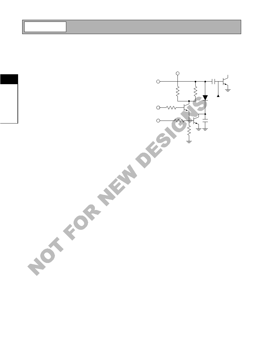
The current through the PIN diode is controlled by two
signals: AT_EN and APC. The AT_EN signal allows
current through the PIN diode and is an on/off function.
The APC signal controls the amount of current through
the PIN diode. Normally, the AT_EN signal will be
derived from the VCO ENABLE signal available in
most GSM handset designs. If maximum isolation is
needed before the ramp-up, the AT_EN signal needs to
be turned on before the RF power is applied to the
device input. The current into this pin is not critical, and
can be reduced to a few hundred micro amps with an
external series resistor. Without the resistor, the pin will
draw about 700
µ
A.
Because of the inverting stage at the APC input, the
current through the PIN diode is inverted from the APC
voltage. Thus, when V
APC
is high for maximum output
power, the attenuator is turned off to obtain maximum
drive level for the first RF stage. When V
APC
is low for
maximum isolation, the attenuator is be turned on to
reduce the drive level and to avoid self-biasing.
The PIN diode is dimensioned such that a low V
APC
the
impedance of the diode is about 50 Ohm. Since the
input impedance of the first RF stage become very
high when the bias is turned off, this topology will main-
tain a good input impedance over the entire V
APC
con-
trol range.
VCC1 and VCC2 provide supply voltage to the first and
second stage, as well as provides some frequency
selectivity to tune to the operating band. Essentially,
5 k
750
500
2 k
RF IN
AT_EN
APC
VCC
From Bias
Stages
PIN

2-135
RF2140
Rev A12 011031
2
PO
W
E
R
A
M
P
LI
FI
E
R
S
See
Upg
ra
ded
P
rod
uct
RF2
17
4
the bias is fed to this pin through a short microstrip. A
bypass capacitor sets the inductance seen by the part,
so placement of the bypass cap can affect the fre-
quency of the gain peak. This supply should be
bypassed individually with 100pF capacitors before
being combined with V
CC
for the output stage to pre-
vent feedback and oscillations.
The RF OUT pin provides the output power. Bias for
the final stage is fed to this output line, and the feed
must be capable of supporting the approximately 1.5A
of current required. Care should be taken to keep the
losses low in the bias feed and output components. A
narrow microstrip line is recommended because DC
losses in a bias choke will degrade efficiency and
power.
While the part is safe under CW operation, maximum
power and reliability will be achieved under pulsed con-
ditions. The data shown in this data sheet is based on
a 12.5% duty cycle and a 600
µ
s pulse, unless speci-
fied otherwise.
The part will operate over a 3.0 V to 5.0V range. Under
nominal conditions, the power at 3.5V will be greater
than +32dBm at +85∞C. As the voltage is increased,
however, the output power will increase. Thus, in a sys-
tem design, the ALC (Automatic Level Control) Loop
will back down the power to the desired level. This
must occur during operation, or the device may be
damaged from too much power dissipation. At 5.0V,
over +36dBm may be produced; however, this level of
power is not recommended, and can cause damage to
the device.
The HBT breakdown voltage is >20 V, so there is no
issue with overvoltage. However, under worst-case
conditions, with the RF drive at full power during trans-
mit, and the output VSWR extremely high, a low load
impedance at the collector of the output transistors can
cause currents much higher than normal. Due to the
bipolar nature of the devices, there is no limitation on
the amount of current the device will sink, and the safe
current densities could be exceeded.
High current conditions are potentially dangerous to
any RF device. High currents lead to high channel tem-
peratures and may force early failures. The RF2140
includes temperature compensation circuits in the bias
network to stabilize the RF transistors, thus limiting the
current through the amplifier and protecting the
devices from damage. The same mechanism works to
compensate the currents due to ambient temperature
variations.
To avoid excessively high currents it is important to
control the V
APC
when operating at supply voltages
higher than 4.0V, such that the maximum output power
is not exceeded.
2-136
RF2140
Rev A12 011031
2
PO
W
E
R
A
M
P
LI
FI
E
R
S
See
Upg
ra
ded
P
rod
uct
RF2
17
4
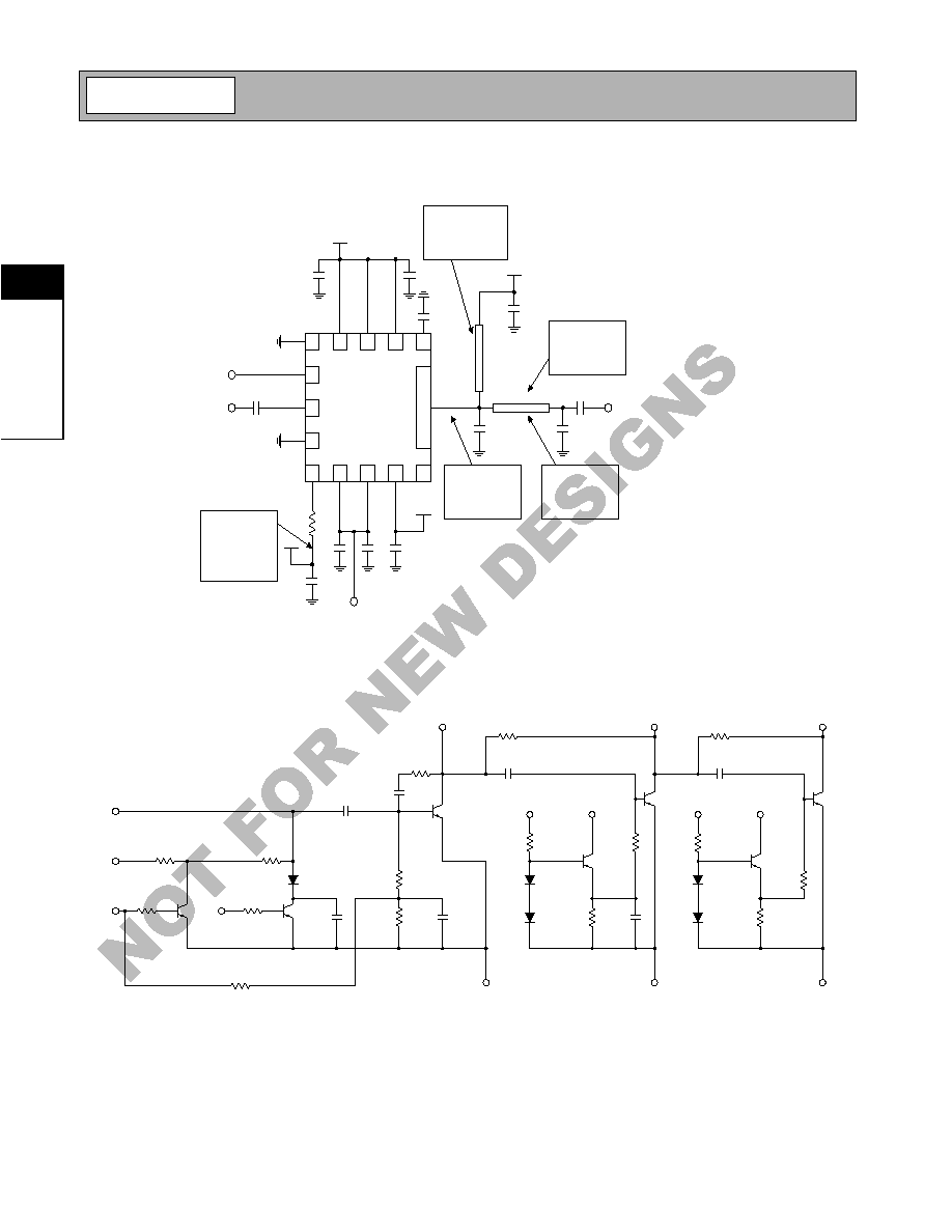
Application Schematic
Internal Schematic
1
2
3
4
5
13
12
11
10
9
AT_EN
RF IN
GND1
RF OUT
6
7
8
16
14
15
VC
C1
AP
C1
AP
C2
VCC
NC
GN
D
2
VC
C2
VC
C2
VC
C2
2F0
15 pF
RF IN
15
pF
V
CC
APC
15
pF
V
CC
5.1 pF
Note 1
50
µ
strip
1.0 pF
Note 1
15 pF
RF OUT
Quarter wave
length
15 pF
V
CC
1.0 pF
1 nF
15pF
Very close to pin 15/16
V
CC
Distance center to
center of
capacitors is
0.220"
Instead of a
stripline an inductor
of ~6 nH can be
used
Instead of a
stripline an
inductor can be
used
Distance between
edge of device
and capacitor is
0.080"
Note: All capacitors are standard
0402 multi layer chip
Note 1: Using a hi-Q capacitor
will increase efficiency slightly
AT_EN
15
pF
15
pF
Distance between
edge of device
and capacitor is
0.240" to improve
the "off" isolation
3.9
RF IN
VCC
APC1
750
5k
500
2k
AT_EN
2.5k
320
1.5k
VCC1
GND1
GND2
APC1
500
2.5k
VCC
VCC2
RF OUT
APC2
200
1.5k
VCC
PKG BASE
2-137
RF2140
Rev A12 011031
2
PO
W
E
R
A
M
P
LI
FI
E
R
S
See
Upg
ra
ded
P
rod
uct
RF2
17
4
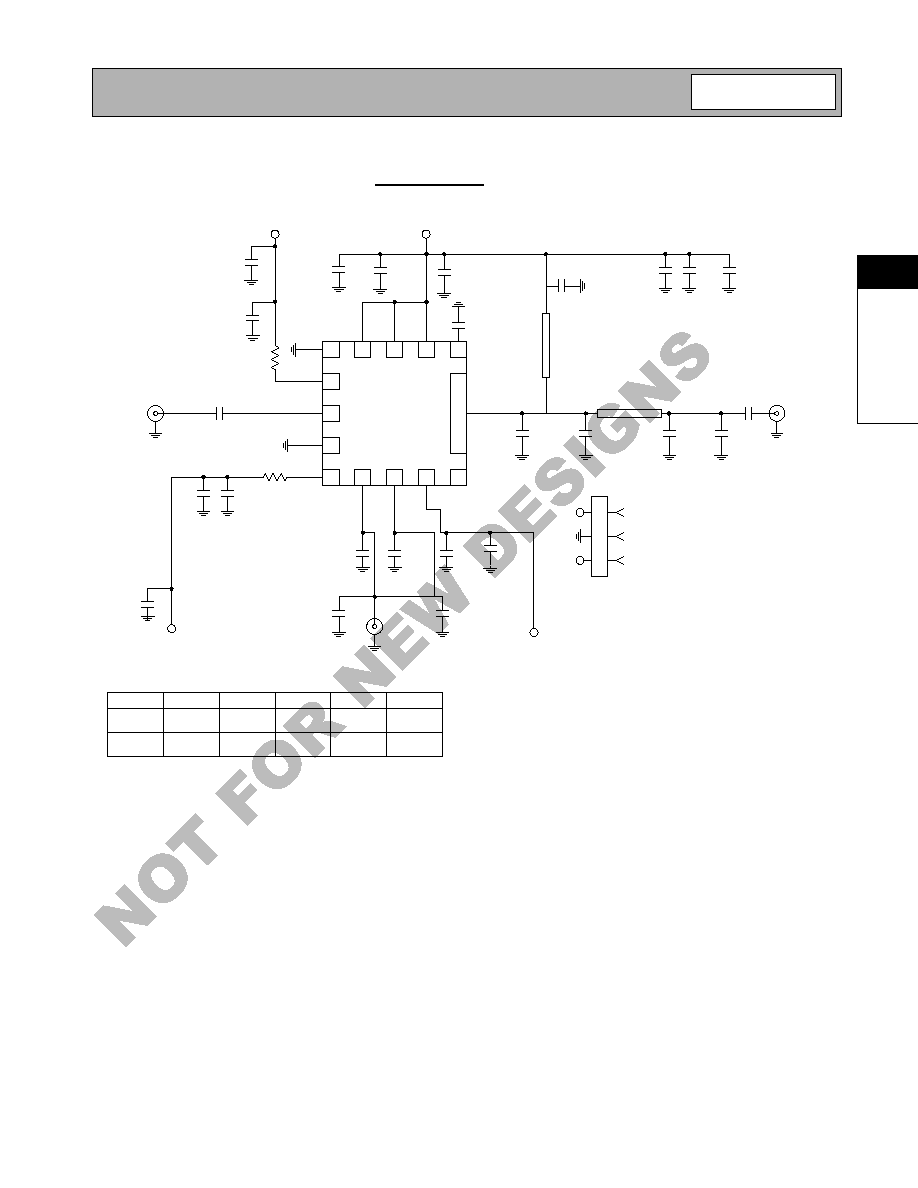
Evaluation Board Schematic
(Download Bill of Materials from www.rfmd.com.)
1
2
3
4
5
13
12
11
10
9
AT_EN
RF IN
GND1
RF OUT
6
7
8
16
14
15
V
CC1
APC
1
APC
2
VC
C
NC
G
ND2
V
CC2
V
CC2
V
CC2
2F0
APC
1
APC
2
VC
C
NC
C1
33 pF
C11
33 pF
C13
33 pF
C14
33 pF
C15
33 pF
C3**
50
µ
strip
.150"
C4**
C2
33 pF
Quarter wave
length
C9
33 pF
C8
1 nF
C10 *
0.9 pF
C6
1 nF
C5 *
12pF
C16
1 nF
C17
1 nF
C7
3.3
µ
F
C12
1 nF
C18
3.3
µ
F
J1
RF IN
J2
RF OUT
P1-1
P1-3
P1-1
P1
ENABL
VCC
1
2
3
GND
P1-3
P1-3
P1-3
Schematic 2140400 Rev A
Board 2140410 Rev A
Capacitors are 0402.
*Murata GRM36COG series
** Johanson 500R07F series
All others are Panasonic ECU series
C20
3.3
µ
F
package
edge to
inside C3
.050"
C19
3.3
µ
F
C21
1nF
C22
1nF
R1
3.9
R3
0
J3
V
APC
C3 (pF)
C4 (pF)
C23 (pF)
5.1
N/I
1.8
N/I
N/I
3.9
0.5
1.2
0.5
0.6
C24 (pF)
C25 (pF)
DCS
Band
PCS
C23**
C24**
C25
2-138
RF2140
Rev A12 011031
2
PO
W
E
R
A
M
P
LI
FI
E
R
S
See
Upg
ra
ded
P
rod
uct
RF2
17
4
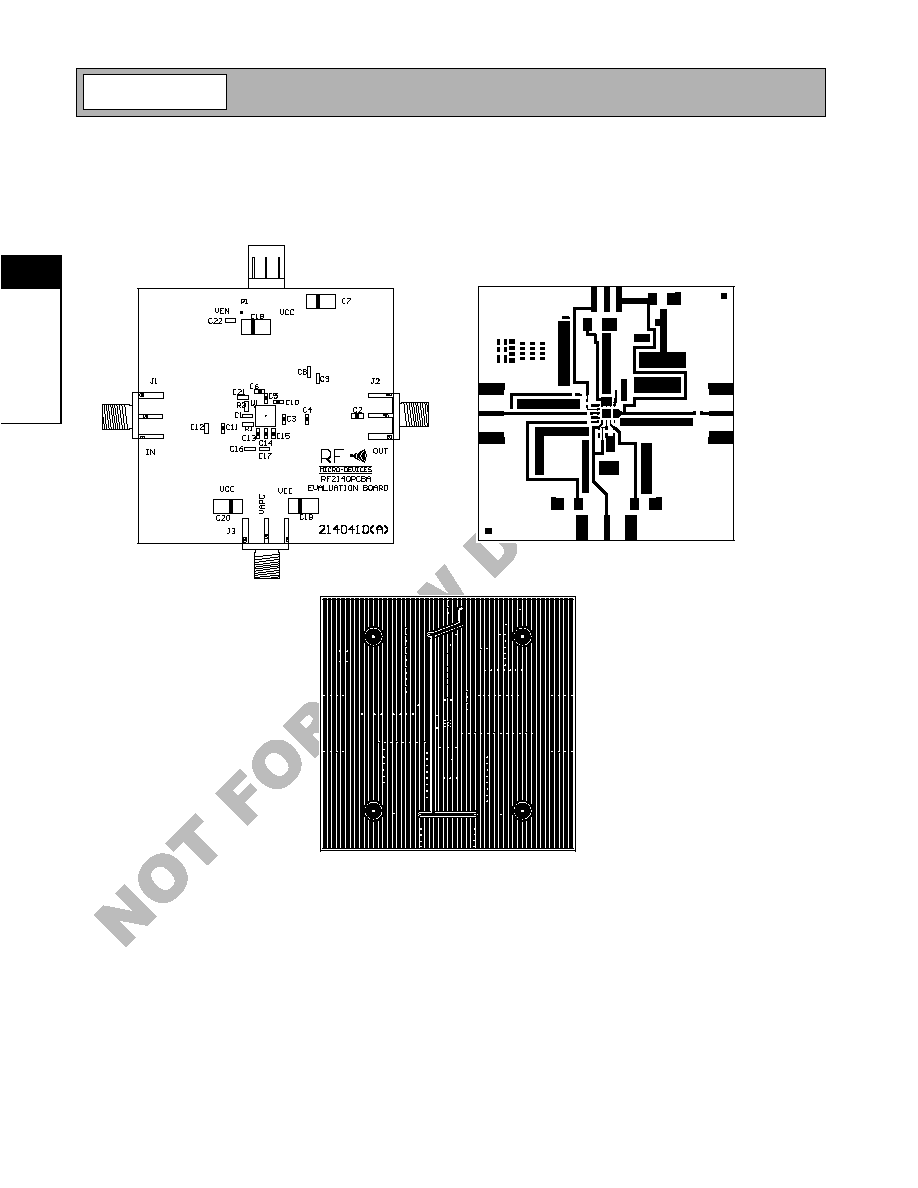
Evaluation Board Layout
Board size 2.0" x 2.0"
Board Thickness 0.014"; Board Material FR-4; Multi-Layer

2-139
RF2140
Rev A12 011031
2
PO
W
E
R
A
M
P
LI
FI
E
R
S
See
Upg
ra
ded
P
rod
uct
RF2
17
4
Typical Test Setup
Power Supply
V- S- S+ V+
10dB/5W
3dB
RF Generator
Spectrum
Analyzer
Buffer
x1 OpAmp
Puls
Generator
A buffer amplifier is recommended because the current into
the Vapc changes with voltage. As an alternative, the
voltage may be monitored with an oscilloscope.
Notes about testing the RF2140
The test setup shown above includes two attenuators. The 3dB pad at the input is to minimize the effects that the
switching of the input impedance of the PA has on the signal generator. When Vapc is switched quickly, the resulting
input impedance change can cause the signal generator to vary its output signal, either in output level or in frequency.
Instead of an attenuator an isolator may also be used. The attenuator at the output is to prevent damage to the spec-
trum analyzer, and should be able to handle the power.
It is important not to exceed the rated supply current and output power. When testing the device at higher than nominal
supply voltage, the V
APC
should be adjusted to avoid the output power exceeding +36 dBm. During load-pull testing at
the output it is important to monitor the forward power through a directional coupler. The forward power should not
exceed +36dBm, and V
APC
needs to be adjusted accordingly. This simulates the behavior for the power control loop in
this respect. To avoid damage, it is recommended to set the power supply to limiting the current during the burst, not to
exceed the maximum current rating.

2-140
RF2140
Rev A12 011031
2
PO
W
E
R
A
M
P
LI
FI
E
R
S
See
Upg
ra
ded
P
rod
uct
RF2
17
4