 | –≠–ª–µ–∫—Ç—Ä–æ–Ω–Ω—ã–π –∫–æ–º–ø–æ–Ω–µ–Ω—Ç: RF2161 | –°–∫–∞—á–∞—Ç—å:  PDF PDF  ZIP ZIP |

¸
2-197
2
PO
W
E
R
A
M
P
LI
FI
E
R
S
Preliminary
Product Description
Ordering Information
Typical Applications
Features
Functional Block Diagram
RF Micro Devices, Inc.
7625 Thorndike Road
Greensboro, NC 27409, USA
Tel (336) 664 1233
Fax (336) 664 0454
http://www.rfmd.com
Optimum Technology MatchingÆ Applied
Si BJT
GaAs MESFET
GaAs HBT
Si Bi-CMOS
SiGe HBT
Si CMOS
1
2
3
4
5
13
12
11
10
9
GND2
VCC1
RFIN
RF OUT
RF OUT
RF OUT
6
7
8
16
14
15
G
ND1
VPD
1
VM
O
D
E
VPD
2
GN
D
V
CC2
V
CC2
V
CC2
VC
C
2F0
RF2161
3V W-CDMA POWER 1900MHZ
3V LINEAR POWER AMPLIFIER
∑ 3V 1850-1910 CDMA-2000 Handsets
∑ 3V 1920-1980 W-CDMA Handsets
∑ Spread Spectrum Systems
∑ Commercial and Consumer Systems
∑ Portable Battery-Powered Equipment
The RF2161 is a high-power, high-efficiency linear ampli-
fier IC targeting 3V handheld systems. The device is
manufactured on an advanced Gallium Arsenide Hetero-
junction Bipolar Transistor (HBT) process, and has been
designed for use as the final RF amplifier in 3V
CDMA-2000 and W-CDMA handsets, spread spectrum
systems, and other applications in the 1920 MHz to
1980 MHz band. The device is self-contained with 50
input and the output can be easily matched to obtain opti-
mum power, efficiency, and linearity characteristics over
all recommended supply voltages.
∑ Single 3V Supply
∑ 27dBm Linear Output Power
∑ 30dB Linear Gain
∑ 35% Linear Efficiency
∑ On-board Power Down Mode
RF2161
3V W-CDMA Power 1900MHZ 3V Linear Power
Amplifier
RF2161 PCBA
Fully Assembled Evaluation Board
2
Rev A3 010514
ALL SOLDER PAD TOLERANCES P0.05mm
1.50 sq.
2.00
0.28
0.13
0.80
0.40
sq.
0.38
1.50
1.20
4.20
3.95
3.50
3.35
4.20
3.95
3.50
3.35
1
Package Style: MP16KO1A
Preliminary
2-198
RF2161
Rev A3 010514
2
PO
W
E
R
A
M
P
LI
FI
E
R
S
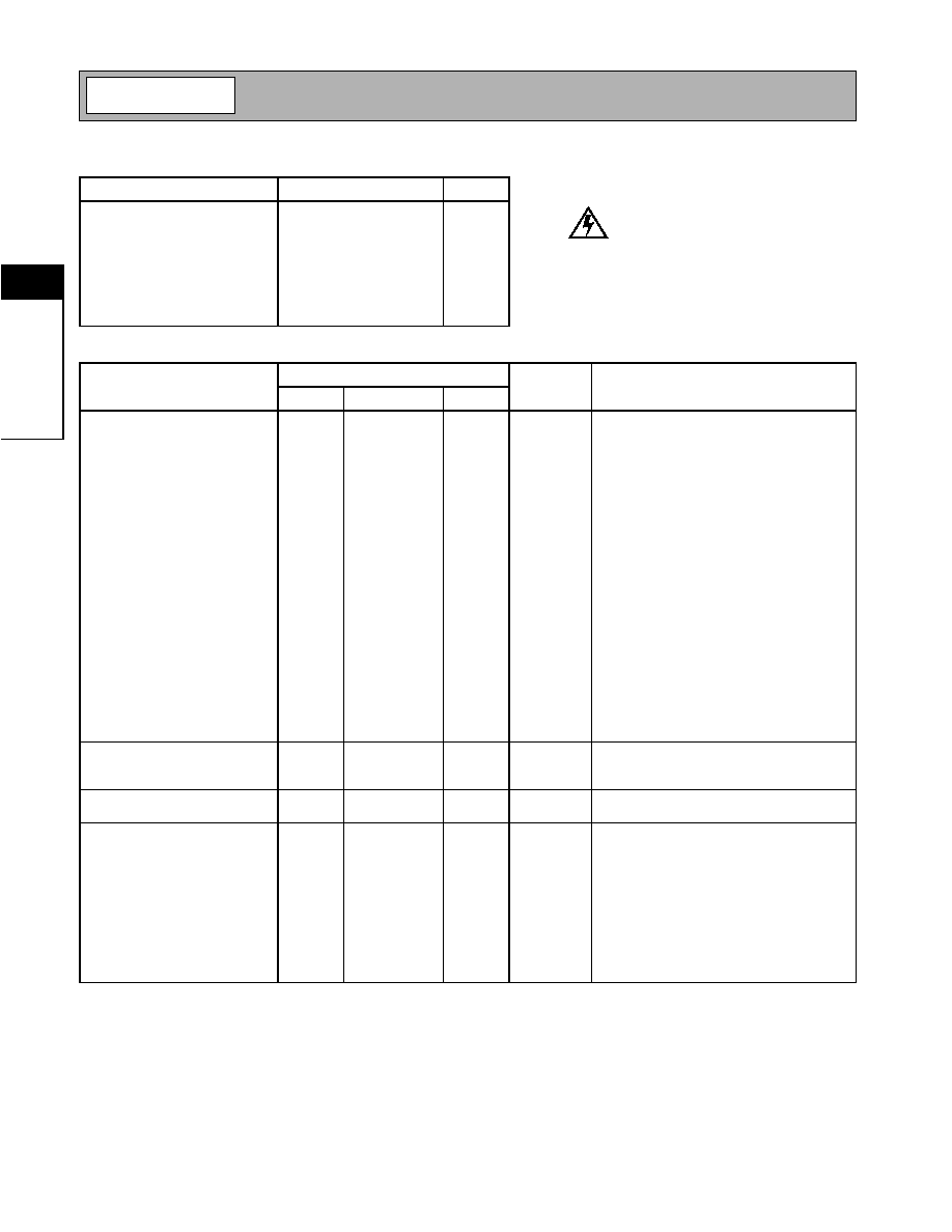
Absolute Maximum Ratings
Parameter
Rating
Unit
Supply Voltage (RF off)
+8.0
V
DC
Supply Voltage (P
OUT
31dBm)
+5.0
V
DC
Mode Voltage (V
MODE
)
+3.0
V
DC
Control Voltage (V
PD
)
+3.0
V
DC
Input RF Power
+6
dBm
Operating Case Temperature
-30 to +100
∞C
Storage Temperature
-30 to +150
∞C
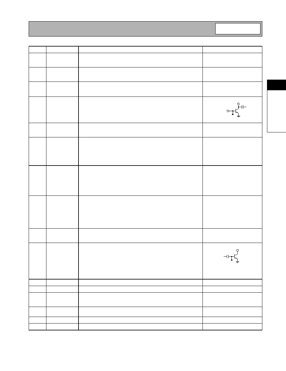
Parameter
Specification
Unit
Condition
Min.
Typ.
Max.
Overall
T = 25 ∞C, V
CC
= 3.4V unless otherwise speci-
fied
Usable Frequency Range
1850
2000
MHz
Typical Frequency Range
1850 to 1910
MHz
1920 to 1980
Linear Gain
28
30
dB
Mode= Low
26
28
dB
Mode= High
Second Harmonic (including
second harmonic trap)
-35
dBc
Third Harmonic
-40
dBc
Fourth Harmonic
-45
dBc
Maximum Linear Output Power
(W-CDMA Modulation)
27
dBm
Total Linear Efficiency
30
35
%
V
MODE
High, P
OUT
=27dBm
Adjacent Channel Power
Rejection@5MHz
-40
-38
dBc
P
OUT
=27dBm, W-CDMA Modulation
3G PP 3.2 03-00 DPCCH+ 1DPDCH
Adjacent Channel Power
Rejection@10MHz
-50
-48
dBc
P
OUT
=27dBm, W-CDMA Modulation
3G PP 3.2 03-00 DPCCH+1DPDCH
Noise Power
-137
dBm/Hz
P
OUT
=+27dBm, Rx Band 2110MHz to
2170MHz
Maximum Linear Output Power
(W-CDMA Modulation)
26
dBm
V
CC
= 3.0V
Total Linear Efficiency
35
%
Input VSWR
< 2:1
Output Load VSWR
5:1
No oscillations
Power Supply
Power Supply Voltage
3.0
3.4
5.0
V
Idle Current
120
mA
MODE = high
V
PD
Current
13
mA
Total pins 6 and 8, V
PD
= 2.8 V
Total Current (Power down)
10
10
µ
A
V
PD
= low
V
PD
"Low" Voltage
0
0.2
V
V
PD
"High" Voltage
2.7
2.8
2.9
V
MODE "High" Voltage
2.5
2.8
MODE "Low" Voltage
0
0.5
Caution! ESD sensitive device.
RF Micro Devices believes the furnished information is correct and accurate
at the time of this printing. However, RF Micro Devices reserves the right to
make changes to its products without notice. RF Micro Devices does not
assume responsibility for the use of the described product(s).
Preliminary
2-199
RF2161
Rev A3 010514
2
PO
W
E
R
A
M
P
LI
FI
E
R
S
Pin
Function
Description
Interface Schematic
1
VCC2
Power supply for second stage and interstage match. Pins 1, 15 and 16
should be connected by a common trace where the pins contact the
printed circuit board.
2
GND2
Ground for second stage. For best performance, keep traces physically
short and connect immediately to ground plane. This ground should be
isolated from the backside ground contact.
3
VCC1
Power supply for first stage and interstage match. V
CC
should be fed
through a 1.2nH inductor terminated with a 8.2pF capacitor on the sup-
ply side. The inductor should be as close to the pin as possible.
See pin 4.
4
RF IN
RF input. An external series capacitor is required as a DC block. The
input match can be improved to <2:1 by using a series capacitor and
shunt inductor.
5
GND1
Ground for first stage. For best performance, keep traces physically
short and connect immediately to ground plane. This ground should be
isolated from the backside ground contact.
See pin 4.
6
VPD1
Power Down control for first and second stages. When this pin is "low",
all first and second stage circuits are shut off. When this pin is 2.8V, all
first and second stage circuits operate normally. V
PD1
requires a regu-
lated 2.8V for the amplifier to operate properly over all specified tem-
perature and voltage ranges. A dropping resistor from a higher
regulated voltage may be used to provide the required 2.8V.
7
VMODE
V
MODE
adjusts the bias to the 2nd and 3rd stages. For full power oper-
ation, MODE is set low. When operating in a lower output power mode
(<+25dBm) this pin is set high to reduce bias current by up to 50%. An
external series resistor is optional to limit the amount of current
required. At low temperature (-30
C), it is recommended to set V
MODE
low to maintain correct operation.
8
VPD2
Power Down control for third stage. When this pin is "low", all and third
stage circuits are shut off. When this pin is 2.8V, all and third stage cir-
cuits operate normally. V
PD
requires a regulated 2.8V for the amplifier
to operate properly over all specified temperature and voltage ranges.
A dropping resistor from a higher regulated voltage may be used to pro-
vide the required 2.8V. A 15pF high frequency bypass capacitor is rec-
ommended.
9
GND
For best performance, keep traces physically short and connect imme-
diately to ground plane. This ground should be isolated from the back-
side ground contact.
10
RF OUT
RF output and power supply for final stage. This is the unmatched col-
lector output of the third stage. A DC block is required following the
matching components. The biasing may be provided via a parallel L-C
set for resonance at the operating frequency of 1920MHz to 1980MHz.
It is important to select an inductor with very low DC resistance with a
1A current rating. Alternatively, shunt microstrip techniques are also
applicable and provide very low DC resistance. Low frequency bypass-
ing is required for stability.
11
RF OUT
Same as pin 10.
See pin 10.
12
RF OUT
Same as pin 10.
See pin 10.
13
2FO
Second harmonic trap. Keep traces physically short and connect imme-
diately to ground plane. This ground should be isolated from backside
ground contact.
14
VCC
Supply for bias reference and control circuits. High frequency bypass-
ing may be necessary.
15
VCC2
Same as Pin 1.
16
VCC2
Same as Pin 1.
GND1
RF IN
VCC1
From Bias
Stages
RF OUT
From Bias
Stages

Preliminary
2-200
RF2161
Rev A3 010514
2
PO
W
E
R
A
M
P
LI
FI
E
R
S
Pin
Function
Description
Interface Schematic
Pkg
Base
GND
Ground connection. The backside of the package should be soldered
to a top side ground pad which is connected to the ground plane with
multiple vias. The pad should have a short thermal path to the ground
plane.

Preliminary
2-201
RF2161
Rev A3 010514
2
PO
W
E
R
A
M
P
LI
FI
E
R
S
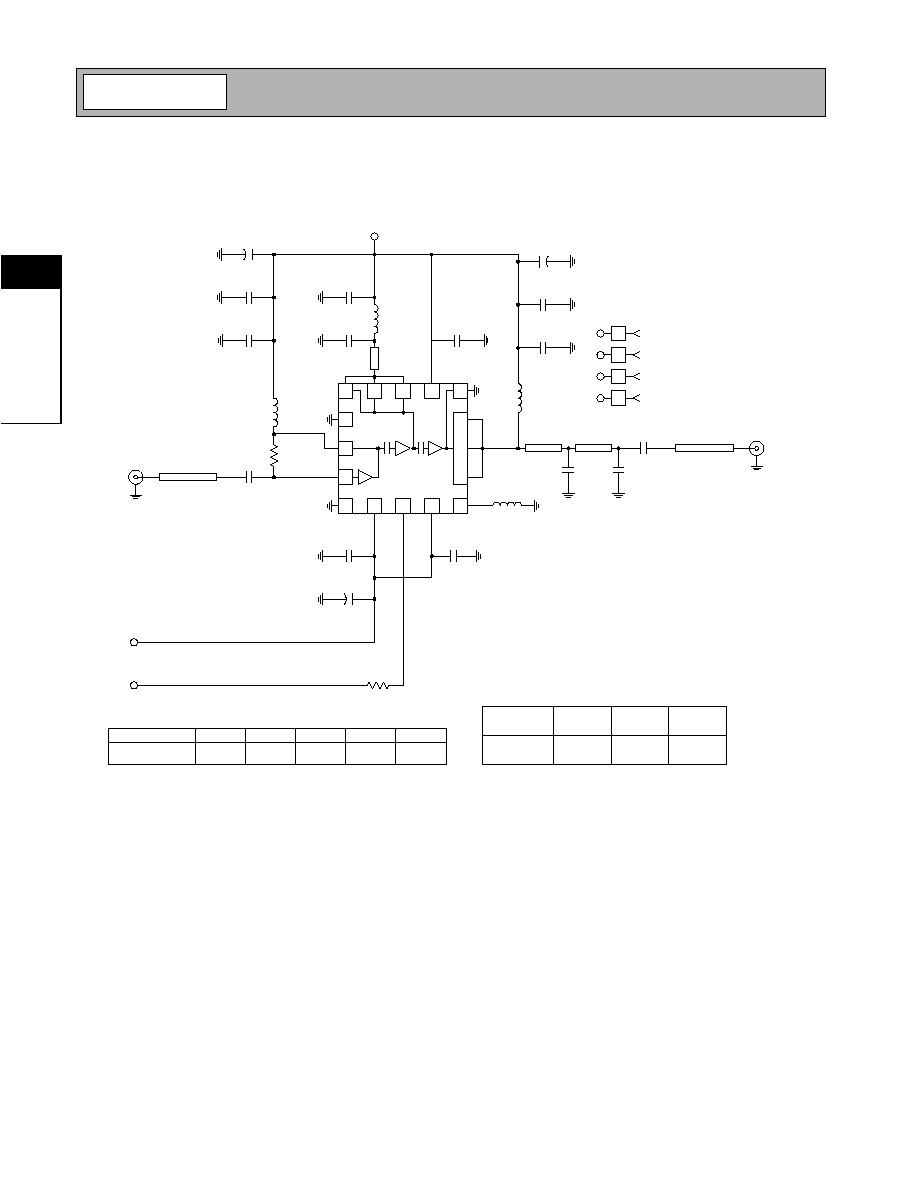
Application Schematic
W-CDMA (1920MHz to 1980MHz)
R2
1.2 nH
8.2 pF
10 nF
C30
10 nF
15 pF
15 pF
RF IN
15 pF
1.8k
15 pF
15 nH
1
2
3
4
5
13
12
11
10
9
6
7
8
16
14
15
VREG
VMODE
V
CC
C1**
C14**
15 pF
RF OUT
L1*
15 pF
10 nF
TL
2
TL
3
* L1 is a High Q inductor (i.e., Coilcraft 0805HQ-series).
**C1 and C14 are High Q capacitors
(i.e., Johanson C-series).
Board
R2 (
)
C14 (pF)
C30 (pF)
C1 (pF)
L1 (nH)
WCDMA
150
2.2
8.2
4.7
16
WCDMA
0.044"
0.140"
0.022"
Transmission
Line Length
TL
1
TL
2
TL
3
TL
1
10 nH
1
µ
F
+
+
1 uF
+
4.7 uF
Preliminary
2-202
RF2161
Rev A3 010514
2
PO
W
E
R
A
M
P
LI
FI
E
R
S
Evaluation Board Schematic
W-CDMA (1920MHz to 1980MHz)
R2
L3
1.2 nH
C11
8.2 pF
C12
10 nF
C30
C8
10 nF
C6
15 pF
C5
15 pF
C27
15 pF
R1
1.8k
C13
15 pF
L4
15 nH
1
2
3
4
5
13
12
11
10
9
6
7
8
16
14
15
P2
P3
C1**
C14**
C3
15 pF
L1*
C4
15 pF
C26
10 nF
TL
2
TL
3
* L1 is a High Q inductor (i.e., Coilcraft 0805HQ-series).
**C1 and C14 are High Q capacitors
(i.e., Johanson C-series).
Board
R2 (
)
C14 (pF)
C30 (pF)
C1 (pF)
L1 (nH)
WCDMA
150
2.2
8.2
4.7
16
WCDMA
0.044"
0.140"
0.022"
Transmission
Line Length
TL
1
TL
2
TL
3
TL
1
50
µ
strip
J2
RF OUT
50
µ
strip
J1
RF IN
P1
2161400-
+
C10
1 uF
+
C7
1
µ
F
L2
10 nH
C2
4.7 uF
+
P3
VMODE
VREG
P2
VCC
P1
P4
GND
Preliminary
2-203
RF2161
Rev A3 010514
2
PO
W
E
R
A
M
P
LI
FI
E
R
S
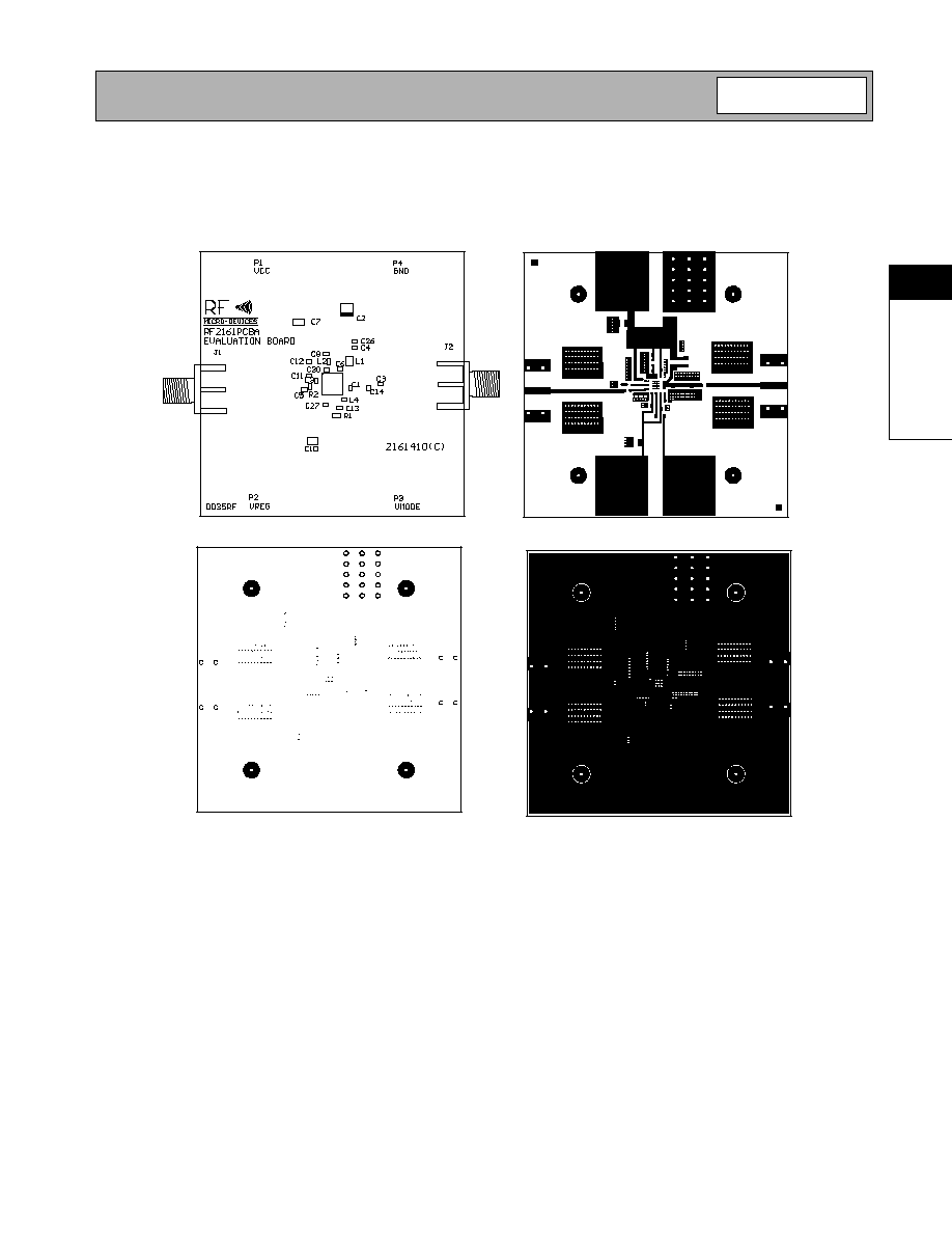
Evaluation Board Layout
Board Size 2.00" x 2.00"
Board Thickness 0.028", Board Material FR-4, Multi-Layer, Ground Plane at 0.014"

Preliminary
2-204
RF2161
Rev A3 010514
2
PO
W
E
R
A
M
P
LI
FI
E
R
S