 | –≠–ª–µ–∫—Ç—Ä–æ–Ω–Ω—ã–π –∫–æ–º–ø–æ–Ω–µ–Ω—Ç: RF2163 | –°–∫–∞—á–∞—Ç—å:  PDF PDF  ZIP ZIP |
2-237
Product Description
Ordering Information
Typical Applications
Features
Functional Block Diagram
RF Micro Devices, Inc.
7628 Thorndike Road
Greensboro, NC 27409, USA
Tel (336) 664 1233
Fax (336) 664 0454
http://www.rfmd.com
Optimum Technology MatchingÆ Applied
Si BJT
GaAs MESFET
GaAs HBT
Si Bi-CMOS
SiGe HBT
Si CMOS
InGaP/HBT
GaN HEMT
SiGe Bi-CMOS
4
PWR SEN
3
BIAS GND2
2
RF IN
1
GND
16
VCC
15
VCC1
14
VCC1
13
NC
5
PW
R REF
6
VREG1
7
VREG2
8
B
I
AS GND 1
9
GND
Bias
12 RF OUT
11 RF OUT
10 RF OUT
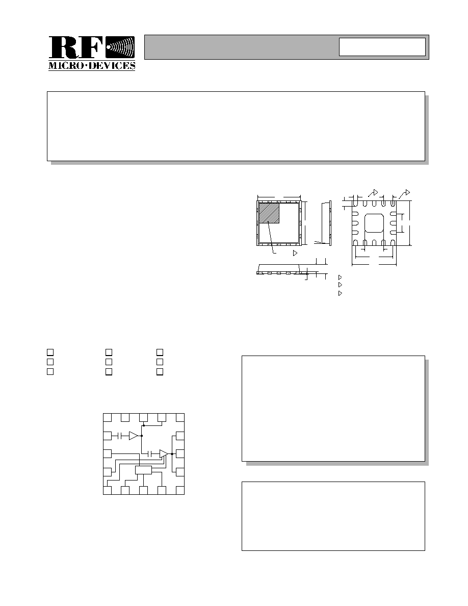
RF2163
3V, 2.5GHz LINEAR POWER AMPLIFIER
∑ 2.5GHz ISM Band Applications
∑ PCS Communication Systems
∑ Wireless LAN Systems
∑ Commercial and Consumer Systems
∑ Portable Battery Powered Equipment
∑ Broadband Spread-Spectrum Systems
The RF2163 is a linear, medium power, high efficiency
amplifier IC designed specifically for low voltage opera-
tion. The device is manufactured on an advanced Gallium
Arsenide Heterojunction Bipolar Transistor (HBT) pro-
cess, and has been designed for use as the final RF
amplifier in 2.5GHz spread-spectrum transmitters. The
device is provided in a 16-pin leadless chip carrier with a
backside ground and is self-contained with the exception
of the output matching network and power supply feed
line.
∑ Single 3.3V Power Supply
∑ +30dBm Saturated Output Power
∑ 19dB Small Signal Gain
∑ High Power Added Efficiency
∑ Patent Pending Power Sense Technology
∑ 1800MHz to 2500MHz Frequency Range
RF2163
3V, 2.5GHz Linear Power Amplifier
RF2163 PCBA
Fully Assembled Evaluation Board
0
Rev A4 030327
3.75
3.75
+
1.50 SQ
4.00
4.00
1
0.45
0.28
3.20
1.60
0.75
0.50
12∞
INDEX AREA
3
1.00
0.90
0.75
0.65
0.05
0.00
NOTES:
5 Package Warpage: 0.05 max.
4 Pins 1 and 9 are fused.
Shaded Pin is Lead 1.
1
Dimension applies to plated terminal and is measured
0.10 mm and 0.25 mm from terminal tip.
2
The terminal #1 identifier and terminal numbering con
shall conform to JESD 95-1 SPP-012. Details of termi
identifier are optional, but must be located within the z
indicated. The identifier may be either a mold or mark
feature.
3
0.80
TYP
2
1
Dimensions in mm.
Package Style: QFN, 16-Pin, 4x4
!
2-238
RF2163
Rev A4 030327
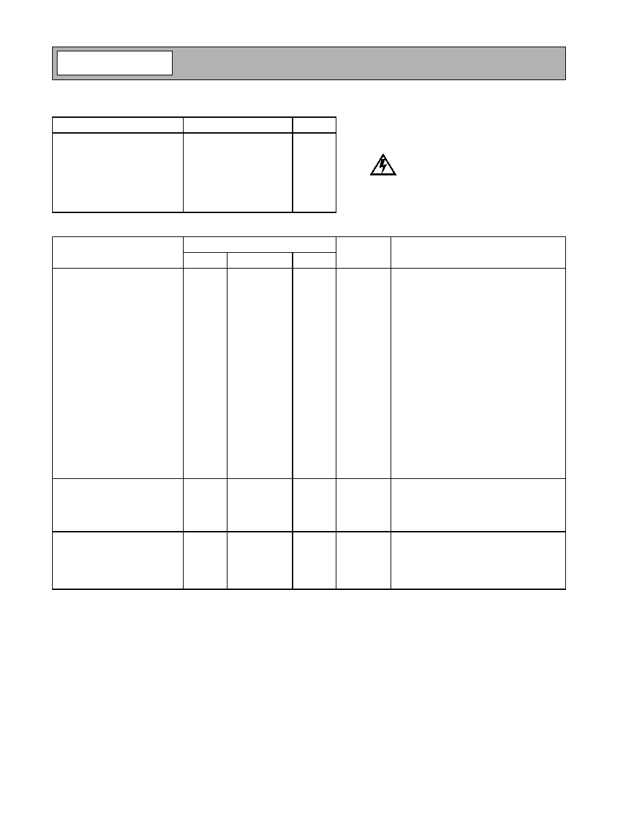
Absolute Maximum Ratings
Parameter
Rating
Unit
Supply Voltage
-0.5 to +6.0
V
DC
Power Control Voltage (V
REG
)
-0.5 to 3.3
V
DC Supply Current
1000
mA
Input RF Power
+15
dBm
Operating Ambient Temperature
-40 to +85
∞C
Storage Temperature
-40 to +150
∞C
Moisture sensitivity
JEDEC Level 3
Parameter
Specification
Unit
Condition
Min.
Typ.
Max.
Overall
T=25 ∞C, V
CC
=3.5V, V
REG1
=V
REG2
=2.3V,
Freq=2450MHz
Frequency Range
1800 to 2500
MHz
Maximum Saturated Output
Power
+29
+30
+32
dBm
P
IN
=+13dBm
Efficiency at Max Output Power
26
%
Maximum Linear Output Power
25
dBm
With 802.11 modulation (11Mbit/s) and
meeting 802.11 spectral mask.
Linear Efficiency
25
%
Small Signal Gain
16
19
dB
P
IN
=10dBm
Reverse Isolation
30
dB
In "ON" state
30
dB
In "OFF" state
Second Harmonic
-35
dBc
Including second harmonic trap, see applica-
tion circuit
Adjacent Channel Power
-35
-32
dBc
P
OUT
=24dBm
Alternate Channel Power
-52
-50
dBc
P
OUT
=24dBm
Isolation
TBD
dBm
In "OFF" state, P
IN
=TBD
Input Impedance
50
With external matching
Input VSWR
2:1
With external matching
Power Down
V
REG
"ON"
2.3
V
Voltage supplied to control input; device is
"ON"
V
REG
"OFF"
0
0.5
V
Voltage supplied to control input; device is
"OFF"
Power Supply
Operating Voltage
3.0 to 5.0
V
Current Consumption
650
mA
Power Down "ON", at max output power
350
mA
Power Down "ON", P
OUT
=25dBm
150
290
mA
Idle current
Caution! ESD sensitive device.
RF Micro Devices believes the furnished information is correct and accurate
at the time of this printing. However, RF Micro Devices reserves the right to
make changes to its products without notice. RF Micro Devices does not
assume responsibility for the use of the described product(s).
Refer to "Handling of PSOP and PSSOP Products"
on page 16-15 for special handling information.

2-239
RF2163
Rev A4 030327
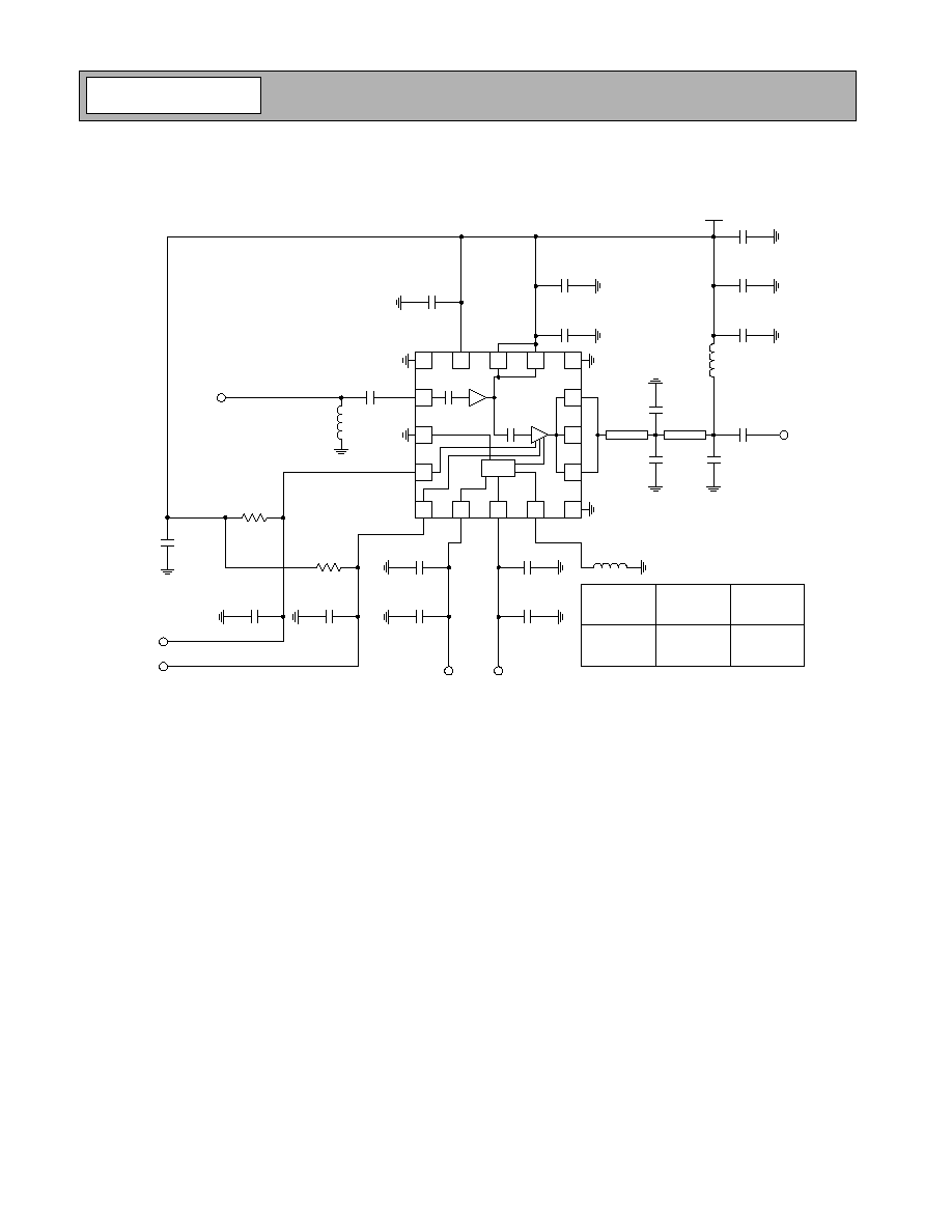
Pin
Function
Description
Interface Schematic
1
GND
Ground connection. For best performance, keep traces physically short
and connect immediately to ground plane.
2
RF IN
RF input. This input is AC coupled, so an external blocking capacitor is
not required if this pin is connected to a DC path.
3
BIAS GND2
Ground for second stage bias circuit. For best performance, keep
traces physically short and connect immediately to ground plane.
See pin 16.
4
PWR SEN
The PWR SEN and PWR REF pins can be used in conjunction with an
external feedback path to provide an RF power control function for the
RF2163. The power control function is based on sampling the RF drive
to the final stage of the RF2163.
5
PWR REF
Same as pin 4.
See pin 4.
6
VREG1
This pin requires a regulated supply to maintain the correct bias cur-
rent.
See pin 16.
7
VREG2
Same as pin 6.
See pin 16.
8
BIAS GND1
Ground for first stage bias circuit. For best performance connect to
ground with a 10nH inductor.
See pin 16.
9
GND
Same as pin 1.
10
RF OUT
RF output and bias for the output stage. The power supply for the out-
put transistor needs to be supplied to this pin. This can be done
through a quarter-wave length microstrip line that is RF grounded at the
other end, or through an RF inductor that supports the required DC cur-
rents.
11
RF OUT
Same as pin 10.
See pin 10.
12
RF OUT
Same as pin 10.
See pin 10.
13
NC
Not connected.
14
VCC1
Interstage match and bias for first stage output. Connect interstage
matching capacitor to t pin with a short trace. Connect low-frequency
bypass capacitors to this pin with a long trace. See evaluation board
layout for details.
See pin 2.
15
VCC1
Same as pin 14.
See pin 2.
16
VCC
Power supply pin for the bias circuits. External low frequency bypass
capacitors should be connected if no other low frequency decoupling is
nearby.
Pkg
Base
GND
Ground connection. The backside of the package should be connected
to the ground plane through a short path, i.e., vias under the device
may be required.
See pin 1 and 2.
RF IN
VCC1
Bond Wire
Inductance
BIAS
RF OUT
PWR SEN
PWR REF
BIAS
RF OUT
BIAS
BIAS
VREG1
VREG2
BIAS
GND1
BIAS
GND2
VCC
2-240
RF2163
Rev A4 030327
Application Schematic
2400MHz to 2483MHz
4
3
2
1
16
15
14
13
5
6
7
8
9
12
11
10
Bias
1.5 pF
1.5 nH
RF IN
390
390
1000 pF
PWR SEN
1000 pF
PWR REF
10 uF
1000 pF
VREG1 VREG2
10 uF
1000 pF
10 nH
3.0 pF
3.0 pF
15 nH
1.5 pF
10 pF
RF OUT
10 pF
1000 pF
10 uF
6.2 pF
1000 pF
1000 pF
1000 pF
V
CC
V
REG1
= 2.4 V
V
REG2
= 2.4 V
V
CC
= 3.5 V
Part is Backside Grounded.
TL1
TL2
Transmission
Line Length
WLAN
TL1
25 mil
175 mil
TL2
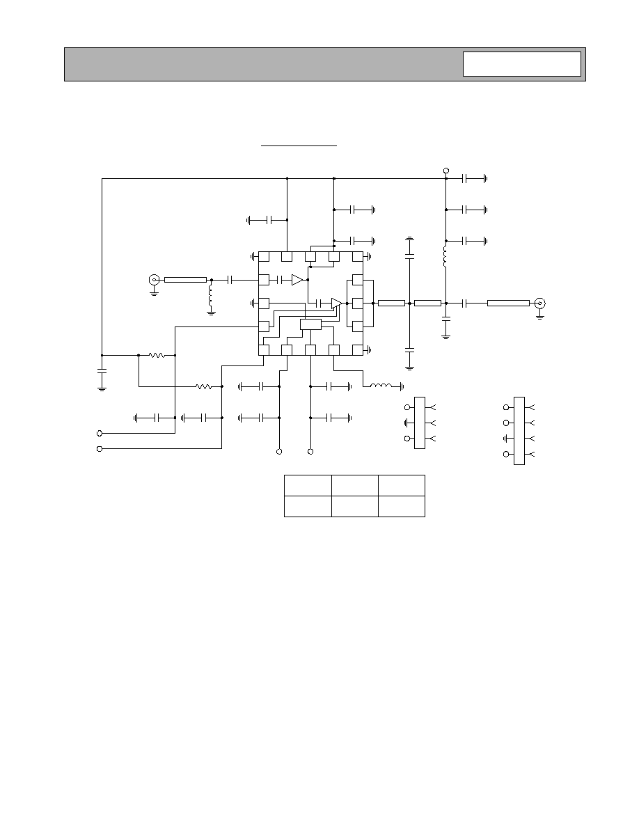
2-241
RF2163
Rev A4 030327
Evaluation Board Schematic
2400MHz to 2483MHz
(Download Bill of Materials from www.rfmd.com.)
4
3
2
1
16
15
14
13
5
6
7
8
9
12
11
10
Bias
C1
1.5 pF
L3
1.5 nH
R2
390
R1
390
C15
1000 pF
P1-3
C16
1000 pF
P1-1
C21
10 uF
C3
1000 pF
P2-2
P2-1
C20
10 uF
C13
1000 pF
L2
10 nH
C6
3.0 pF
C5
3.0 pF
L1
15 nH
C7
1.5 pF
C8
10 pF
C9
10 pF
C10
1000 pF
C22
10 uF
C11
6.2 pF
C4
1000 pF
C2
1000 pF
V
REG1
= 2.3 V
V
REG2
= 2.3 V
V
CC
= 3.5 V
Part is Backside Grounded.
C12
1000 pF
2163400-
P1
1
2
3
GND
P1-1
PS REF
P1-3
PWR SENSE
P2
1
2
3
4
GND
P2-2
VREG1
P2-4
VCC
P2-1
VREG2
TL1
TL2
J1
RF IN
50
µ
strip
P2-4
Transmission
Line Length
TL1
TL2
WLAN
25 mil
175 mil
50
µ
strip
J2
RF OUT

2-242
RF2163
Rev A4 030327
Evaluation Board Layout
Board Size 2.0" x 2.0"
Board Thickness 0.028", Board Material FR-4

2-243
RF2163
Rev A4 030327
Theory of Operation and Application Information
The RF2163 is a two-stage device with a nominal gain of 19dB in the 2.4GHz to 2.5GHz ISM band. The RF2163 is
designed primarily for IEEE802.11B WLAN applications where the available supply voltage and current are not limited. It
will meet 802.11B spectral mask requirements at an output power of +24dBm. It is especially appropriate for WLAN
access points and other base-station type equipment.
The RF2163 requires only a single positive supply of 3.3V nominal (or greater) to operate to full specifications. Power
control is provided through two bias control input pins (V
REG1
and V
REG2
), but in most applications these are tied
together and used as a single control input.
There is some external matching on the input and output of the part, thus allowing the part to be used in other applica-
tions outside the 2.4GHz to 2.5GHz ISM band (such as MMDS). Both the input and the output of the device need a
series DC-blocking capacitor. In some cases, a capacitor used as a matching component can also serve as the blocking
cap. The circuit used on the evaluation board is optimized for 3.5V nominal applications.
For best results, the PA circuit layout from the evaluation board should be copied as closely as possible, particularly the
ground layout and ground vias. Other configurations may also work, but the design process is much easier and quicker if
the layout is copied from the RF2163 evaluation board. Gerber files of our designs can be provided upon request.
The RF2163 is not a difficult part to implement, but care in circuit layout and component selection is always advisable
when designing circuits to operate at 2.5GHz. The most critical passive components in the circuit are the input, inter-
stage and output matching components (C1, C5, C6, C7, and C11). In these cases, high-Q capacitors suitable for RF
applications are used on our evaluation board (a BOM is available on request). High-Q parts are not required in every
design, but it is very strongly recommended that the original design be implemented with the same or similar parts used
on our evaluation board. Then, less costly components can be substituted in their place, making it easy to test the impact
of cheaper components on performance. General RFMD experience has indicated that the slightly higher cost of better
quality passive components is more than offset by the significant improvements in production yields in large-volume
manufacturing.
The interstage matching capacitor, C11, along with the combined inductance of the internal bond wire, the short length
of circuit board trace, and the parasitic inductance of this capacitor, tunes the peak of the small-signal gain response.
The trace length between C11 and pins 14 and 15 should be kept as short as possible.
In practice, V
CC1
, V
CC
, and the supply for the output stage bias will be tied to this supply line. This can be accomplished
using a suitably-long transmission line which is RF shorted on the other end. Ideally the length of this line will be a quar-
ter wavelength, but it only needs to be long enough so that the effects of other supply bypass capacitors on the inter-
stage match are minimized. If board space is a concern, this isolation can also be accomplished with an RF choke
inductor or ferrite bead. Additionally, a higher-value capacitor than shown on the application schematic can be used if
bypass capacitors must be closer. A Smith Chart can be used to provide initial guidance for value selection and parts
placement. Be aware of the self-resonant frequency (SRF) of higher-valued capacitors. The SRF must be above the fre-
quency of operation.
The output matching caps are C5, C6, and C7. These are tuned along with the 50
transmission line segments TL1 and
TL2, as shown on the evaluation board schematic. These segments should be duplicated as closely as possible. Due to
variations in FR-4 characteristics and PCB manufacturer process variations, some benefit will be obtained from small
adjustments to these transmission line lengths when the evaluation board layout is duplicated on another design. Prior to
full rate manufacturing, the board layout of early prototypes should include some additional exposed ground areas
around C5, C6, and C7 to optimize this part of the circuit. In order to reduce component count, the output can also be
tuned with a single capacitor. A Smith Chart can help determine the desired value and transmission line length, which
can be similarly adjusted on the board prior to production. This will result in a slightly lower-bandwidth and more sensi-
tive match, but in most applications the bandwidth is still sufficient.

2-244
RF2163
Rev A4 030327
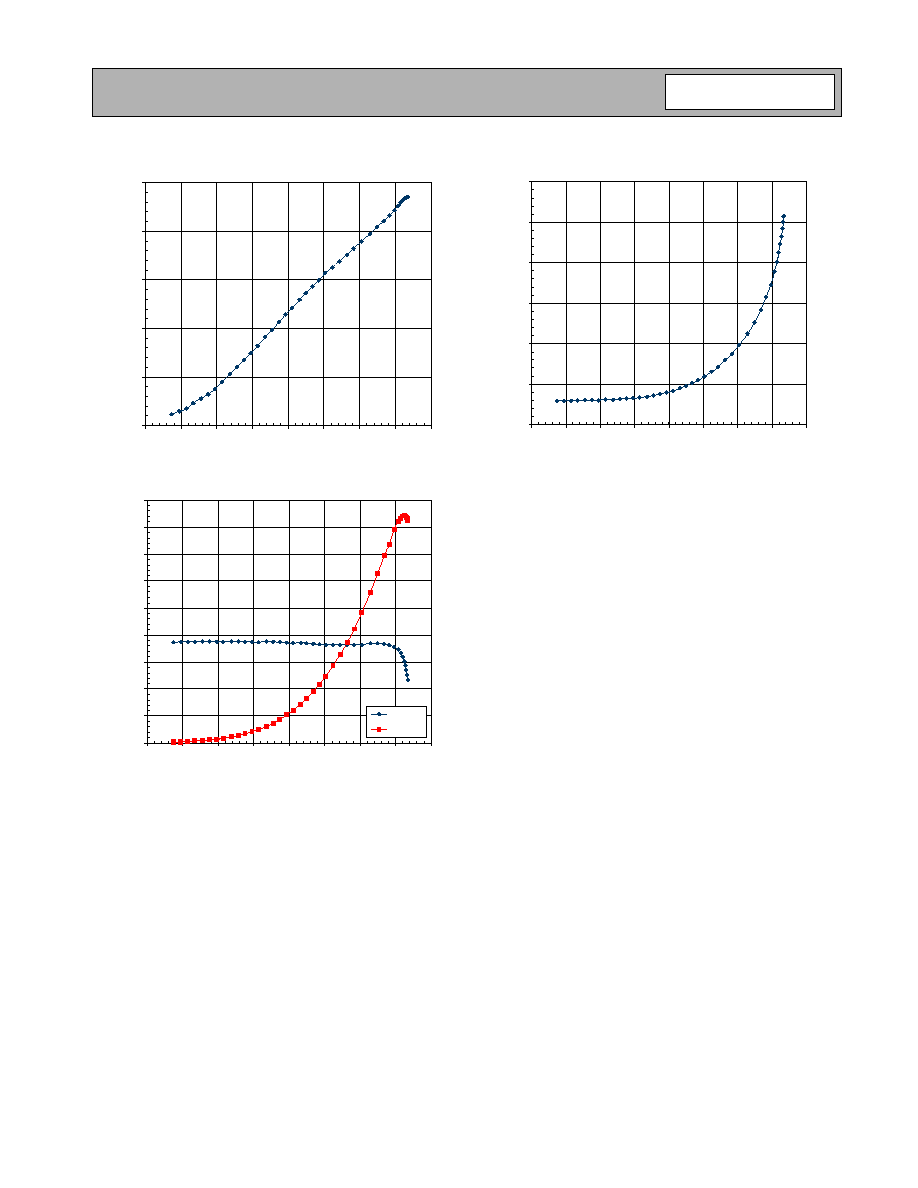
Power sensing is implemented with the PWR SEN and PWR REF lines. The outputs of these pins are transistor collec-
tors and need to be pulled up to the supply through a resistor. PWR REF provides an output current proportional to the
output stage bias current, and PWR SEN provides an output current proportional to the total (RF and bias) current of the
output stage. The pulllup resistors convert these currents to voltages, and the voltage difference between these two pins
is proportional to the RF current. See the graph, "V
REF
-V
SENSE
versus P
OUT
", for the response of this signal. This differ-
ence signal can be fed to a power control circuit elsewhere in the end product, or it can be processed at the PA with addi-
tional circuitry and used to adjust the V
REG
voltage(s) to implement automatic level control. Contact RFMD Sales or
Applications Engineering for additional data and guidance in using this feature.
The RF2163 has primarily been characterized with a voltage on V
REG1
and V
REG2
of 2.4VDC. However, the RF2163 will
operate from a wide range of control voltages. If you prefer to use a control voltage that is significantly different than
2.4VDC, contact RFMD Sales or Applications Engineering for additional data and guidance.
2-245
RF2163
Rev A4 030327
I
CC
versus P
OUT
0.0
200.0
400.0
600.0
800.0
1000.0
1200.0
-5.0
0.0
5.0
10.0
15.0
20.0
25.0
30.0
35.0
P
OUT
(dBm)
I
CC
(mA)
V
REF
- V
SENSE
versus P
OUT
-2.0
-1.5
-1.0
-0.5
0.0
0.5
-5.0
0.0
5.0
10.0
15.0
20.0
25.0
30.0
35.0
P
OUT
(dBm)
Log10 (V
REF
-V
SENSE
)
Gain and Efficiency versus P
OUT
with 802.11 Modulation
0.0
5.0
10.0
15.0
20.0
25.0
30.0
35.0
40.0
45.0
-5.0
0.0
5.0
10.0
15.0
20.0
25.0
30.0
35.0
P
OUT
(dBm)
Gain, Efficiency (dB, %)
Gain (dB)
Eff

2-246
RF2163
Rev A4 030327