¸
2-249
2
PO
W
E
R
A
M
P
LI
FI
E
R
S
Preliminary
Product Description
Ordering Information
Typical Applications
Features
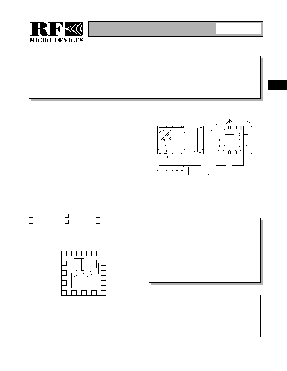
Functional Block Diagram
RF Micro Devices, Inc.
7628 Thorndike Road
Greensboro, NC 27409, USA
Tel (336) 664 1233
Fax (336) 664 0454
http://www.rfmd.com
Optimum Technology MatchingÆ Applied
Si BJT
GaAs MESFET
GaAs HBT
Si Bi-CMOS
SiGe HBT
Si CMOS
13
12
11
10
9
8
16
14
15
1
2
3
4
5
7
6
Bias
Circuits
NC
NC
GND
RF
IN
VP
C
GND
NC
GND
NC
V
CC1
V
CC2
V
CC2
GND
NC
RF OUT
RF OUT
RF2189
3V, 2.5GHZ LINEAR POWER AMPLIFIER
∑ 2.5GHz ISM Band Applications
∑ PCS Communication Systems
∑ Wireless LAN Systems
∑ Commercial and Consumer Systems
∑ Portable Battery-Powered Equipment
∑ Broadband Spread-Spectrum Systems
The RF2189 is a linear, medium-power, high-efficiency
amplifier IC designed specifically for low voltage opera-
tion. The device is manufactured on an advanced Gallium
Arsenide Heterojunction Bipolar Transistor (HBT) pro-
cess, and has been designed for use as the final RF
amplifier in 2.5 GHz spread-spectrum transmitters. The
device is provided in a 16-pin leadless chip carrier with a
backside ground and is self-contained with the exception
of the output matching network and power supply feed
line.
∑ Single 3.3V Power Supply
∑ +25dBm Saturated Output Power
∑ 20dB Small Signal Gain
∑ High Power Added Efficiency
∑ Power Down Mode
∑ 1800MHz to 2500MHz Frequency Range
RF2189
3V, 2.5GHz Linear Power Amplifier
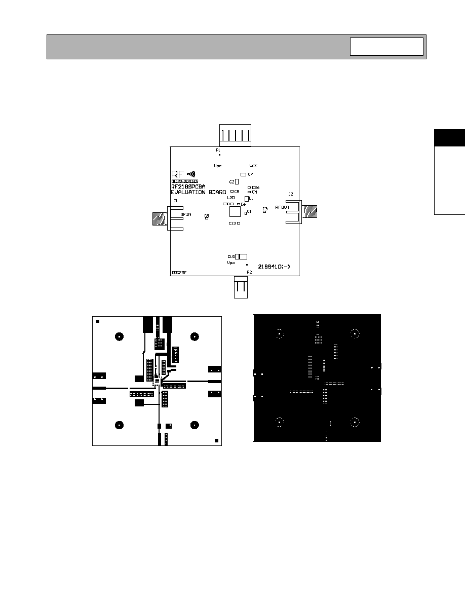
RF2189 PCBA
Fully Assembled Evaluation Board
2
Rev A4 010424
3.75
3.75
+
1.50 SQ
4.00
4.00
1
0.45
0.28
3.20
1.60
0.75
0.50
12∞
INDEX AREA 3
1.00
0.90
0.75
0.65
0.05
0.00
NOTES:
5
Package Warpage: 0.05 max.
4
Pins 1 and 9 are fused.
Shaded Pin is Lead 1.
1
Dimension applies to plated terminal and is measured between
0.10 mm and 0.25 mm from terminal tip.
2
The terminal #1 identifier and terminal numbering convention
shall conform to JESD 95-1 SPP-012. Details of terminal #1
identifier are optional, but must be located within the zone
indicated. The identifier may be either a mold or marked
feature.
3
0.80
TYP
2
1
Dimensions in mm.
Package Style: LCC, 16-Pin, 4x4
Preliminary
2-250
RF2189
Rev A4 010424
2
PO
W
E
R
A
M
P
LI
FI
E
R
S
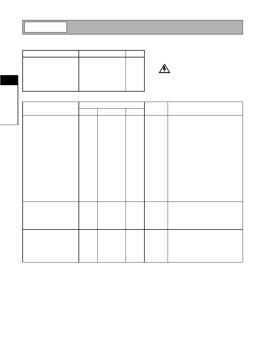
Absolute Maximum Ratings
Parameter
Rating
Unit
Supply Voltage
-0.5 to +6.0
V
DC
Power Control Voltage (V
PC
)
-0.5 to 3.3
V
DC Supply Current
350
mA
Input RF Power
+12
dBm
Operating Ambient Temperature
-40 to +85
∞C
Storage Temperature
-40 to +150
∞C
Moisture sensitivity
JEDEC Level 3
Parameter
Specification
Unit
Condition
Min.
Typ.
Max.
Overall
T = 25 ∞C, V
CC
= 3.3V, V
PC
=3.0V, P
IN
=0dBm,
Freq= 2450MHz
Frequency Range
1800 to 2500
MHz
Maximum Saturated Output
Power
+23
+24
+26
dBm
P
IN
=+6dBm
Efficiency at Max Output Power
42
%
Small Signal Gain
19
20
dB
Reverse Isolation
30
dB
In "ON" state
30
dB
In "OFF" state
Second Harmonic
-50
dBc
Including second harmonic trap, see applica-
tion circuit
IM
3
-30
-23
dBm
P
OUT
= +17dBm in each tone
IM
5
-35
-30
dBm
P
OUT
= +17dBm in each tone
IM
7
-48
-35
dBm
P
OUT
= +17dBm in each tone
Isolation
-20
-30
dBm
In "OFF" state, P
IN
=0dBm
Input Impedance
50
Input VSWR
2:1
Noise Figure
7
dB
Power Down
Power Control "ON"
2.7
3.0
V
Voltage supplied to control input; device is
"ON"
Power Control "OFF"
0
0.5
V
Voltage supplied to control input; device is
"OFF"
PC Input Impedance
5
k
Power Supply
Operating Voltage
3.0 to 5.0
V
Current Consumption
180
260
320
mA
Power Down "ON", at max output power
95
150
175
mA
Power Down "ON", two-tone test +20dBm
average output power
50
100
150
mA
Idle current
Current Consumption
<1
10
µ
A
Power Down "OFF"
Caution! ESD sensitive device.
RF Micro Devices believes the furnished information is correct and accurate
at the time of this printing. However, RF Micro Devices reserves the right to
make changes to its products without notice. RF Micro Devices does not
assume responsibility for the use of the described product(s).
Refer to "Handling of PSOP and PSSOP Products"
on page 16-15 for special handling information.

Preliminary
2-251
RF2189
Rev A4 010424
2
PO
W
E
R
A
M
P
LI
FI
E
R
S
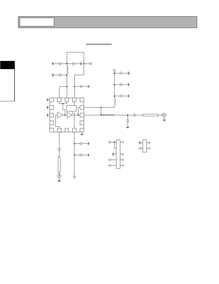
Pin
Function
Description
Interface Schematic
1
GND
Ground connection. Keep traces physically short and connect immedi-
ately to ground plane for best performance.
2
GND
Same as pin 1.
3
GND
Same as pin 1.
4
NC
Not connected.
5
NC
Not connected.
6
RF IN
RF input. This input is DC coupled, so an external blocking capacitor is
required if this pin is connected to a DC path.
See pin 1.
7
NC
Not connected.
8
PC
Power control pin. For maximum power this pin should be 3.3V. A
higher voltage is not recommended. For less output power and reduced
idle current this voltage may be reduced.
9
GND
Ground connection. Keep traces physically short and connect immedi-
ately to ground plane for best performance.
10
NC
Not internally connected.
11
RF OUT
RF output and bias for the output stage. The power supply for the out-
put transistor needs to be supplied to this pin. This can be done
through a quarter-wave length microstrip line that is RF grounded at the
other end, or through an RF inductor that supports the required DC cur-
rents.
12
RF OUT
Same as pin 11.
See pin 11.
13
NC
Not connected.
14
VCC1
Power supply pin for the bias circuits. External low frequency bypass
capacitors should be connected if no other low frequency decoupling is
nearby.
See pin 5.
15
VCC2
Bias supply pin for the first stage. A small tuning capacitor is required to
set the desired frequency response. External low frequency bypass
capacitors should be connected as shown in the application schematic
if no other low frequency decoupling is nearby.
16
VCC2
Connected internally to pin 15.
See pin 15.
Pkg
Base
GND
Ground connection. The backside of the package should be connected
to the ground plane through a short path, i.e., vias under the device
may be required.
See pin 1 and 6.
PC
500
VCC1
To RF
Stages
RF OUT
RF IN
BIAS
VCC2
Preliminary
2-252
RF2189
Rev A4 010424
2
PO
W
E
R
A
M
P
LI
FI
E
R
S
Evaluation Board Schematic
(Download Bill of Materials from www.rfmd.com.)
13
9
10
11
12
1
5
4
3
2
7
8
6
15
14
16
Bias
Circuits
C5
15 pF
J1
RF IN
50
µ
strip
VPC
C15
22 uF
C13
10 nF
P2
1
2
CON2
P2-2
VPC
GND
C4
22 pF
L1
3.3 nH
C7
1
µ
F
C26
100 pF
VCC
C1
2.2 pF
C3
15 pF
50
µ
strip
J2
RF OUT
C6
10 pF
C30
9 pF
C8
10 nF
C2
1 nF
VCCT
L2
1 k
Ferrite
P1
1
2
3
4
5
CON5
VCC
P1-5
VCC
P1-4
GND
P1-1
VPC
Preliminary
2-253
RF2189
Rev A4 010424
2
PO
W
E
R
A
M
P
LI
FI
E
R
S
Evaluation Board Layout
Board Size 2.0" x 2.0"
Board Thickness 0.031"; Board Material FR-4

Preliminary
2-254
RF2189
Rev A4 010424
2
PO
W
E
R
A
M
P
LI
FI
E
R
S