 | –≠–ª–µ–∫—Ç—Ä–æ–Ω–Ω—ã–π –∫–æ–º–ø–æ–Ω–µ–Ω—Ç: RF2367 | –°–∫–∞—á–∞—Ç—å:  PDF PDF  ZIP ZIP |

¸
4-193
4
G
E
N
E
RA
L
P
URPO
SE
A
M
P
L
IF
IE
RS
Preliminary
Product Description
Ordering Information
Typical Applications
Features
Functional Block Diagram
RF Micro Devices, Inc.
7625 Thorndike Road
Greensboro, NC 27409, USA
Tel (336) 664 1233
Fax (336) 664 0454
http://www.rfmd.com
Optimum Technology MatchingÆ Applied
Si BJT
GaAs MESFET
GaAs HBT
Si Bi-CMOS
SiGe HBT
Si CMOS
PD
GND
RF OUT
GND
GND
RF IN
1
2
3
6
4
5
RF2367
PCS CDMA/TDMA/GSM1800
3V PA DRIVER AMPLIFIER
∑ TDMA/CDMA/FM PCS Tx Amplifier
∑ Low Noise Transmit Driver Amplifier
∑ 2.4GHz WLAN Systems
∑ GSM1800 Driver Amplifier
∑ General Purpose Amplification
∑ Commercial and Consumer Systems
The RF2367 is a low noise CDMA/TDMA/GSM PA driver
amplifier with a very high dynamic range designed for
transmit digital PCS applications with frequency ranges
between 1700MHz and 2000MHz. The device functions
as an outstanding PA driver amplifier in the transmit chain
of digital subscriber units where low transmit noise power
is a concern. The IC includes a power down feature that
can be used to completely turn off the device. The
RF2367 is featured in a standard SOT23-6 plastic pack-
age.
∑ Low Noise and High Intercept Point
∑ Adjustable Bias Current
∑ Power Down Control
∑ Single 2.5V to 6.0V Power Supply
∑ 150MHz to 2500MHz Operation
∑ Extremely Small SOT23-6 Package
RF2367
PCS CDMA/TDMA/GSM1800 3V PA Driver Amplifier
RF2367 PCBA
Fully Assembled Evaluation Board
4
Rev A1 010619
.90
.70
.10 MAX.
1.30
1.00
3.10
2.70
.37 MIN.
3.00
2.60
1.90
.25
.10
.50
.35
1.80
1.40
9∞
67XY
All dimensions in mm.
1∞
P
IN
1
Package Style: SOT23-6
Preliminary
4-194
RF2367
Rev A1 010619
4
G
E
N
E
RA
L
P
URPO
SE
A
M
P
L
IF
IE
RS
Absolute Maximum Ratings
Parameter
Rating
Unit
Supply Voltage
-0.5 to +8.0
V
DC
Input RF Level
+10
dBm
Storage Temperature
-40 to +150
∞C
Parameter
Specification
Unit
Condition
Min.
Typ.
Max.
Operating Range
Overall Frequency Range
150 to 2500
MHz
Supply Voltage (V
CC
)
2.5
6.0
V
Power Down Voltage (V
PD
)
2.7
2.9
V
For normal operation
0.9
V
For power down operation
Total Current Consumption
24
37
45
mA
V
CC
= 3.0V, V
PD
= 2.8V
10
µ
A
V
CC
= 3.0V, V
PD
< 0.9V
Operating Ambient Temperature
-40
+85
o
C
Input Impedance
50
Output Impedance
50
1880 MHz Performance
All parameters measured from evaluation
board with T = 25∞C, RF = 1880MHz,
V
CC
= 3.0V, V
PD
= 2.8V
Gain
20
21.5
23
dB
Output IP3
+20
+24
dBm
Noise Figure
2.2
2.5
dB
Reverse Isolation
32
34
dB
Input VSWR
1.9:1
2:1
Output VSWR
1.5:1
2:1
Using External LC network used on Evalua-
tion Board
Output P
1dB
+13
+14
+15
dBm
Caution! ESD sensitive device.
RF Micro Devices believes the furnished information is correct and accurate
at the time of this printing. However, RF Micro Devices reserves the right to
make changes to its products without notice. RF Micro Devices does not
assume responsibility for the use of the described product(s).

Preliminary
4-195
RF2367
Rev A1 010619
4
G
E
N
E
RA
L
P
URPO
SE
A
M
P
L
IF
IE
RS
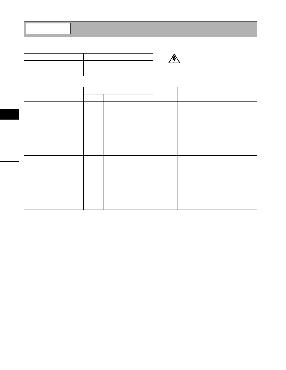
Pin
Function
Description
Interface Schematic
1
GND
Ground connection. Keep traces physically short and connect immedi-
ately to ground plane for best performance.
2
GND
Same as pin 1.
3
RF IN
RF input pin. This pin is DC coupled and internally matched to a <2:1
VSWR at 1880MHz.
4
PD
Power Down for the IC. V
PD
= 2.8V +/- 0.1V turns on the Part.
V
PD
<0.9V turns off the Part. Lower threshold for device operation is
approximately 1.2V. External RF bypassing is required. The trace
length between the pin and the bypass capacitors should be minimized.
The ground side of the bypass capacitors should connect immediately
to ground plane. Nominal current for this pin for V
PD
= 2.8V is 8mA typ-
ical.
See pin 3.
5
GND
Same as pin 1.
6
RF OUT
Amplifier Output pin. This pin is an open-collector output. It must be
biased to either V
CC
or pin 4 through a choke or matching inductor.
This pin is typically externally matched to 50
with a shunt bias/match-
ing inductor and series blocking/matching capacitor. Refer to applica-
tion/evaluation board schematics.
RF IN
PD
TO OUTPUT
STAGE
Preliminary
4-196
RF2367
Rev A1 010619
4
G
E
N
E
RA
L
P
URPO
SE
A
M
P
L
IF
IE
RS
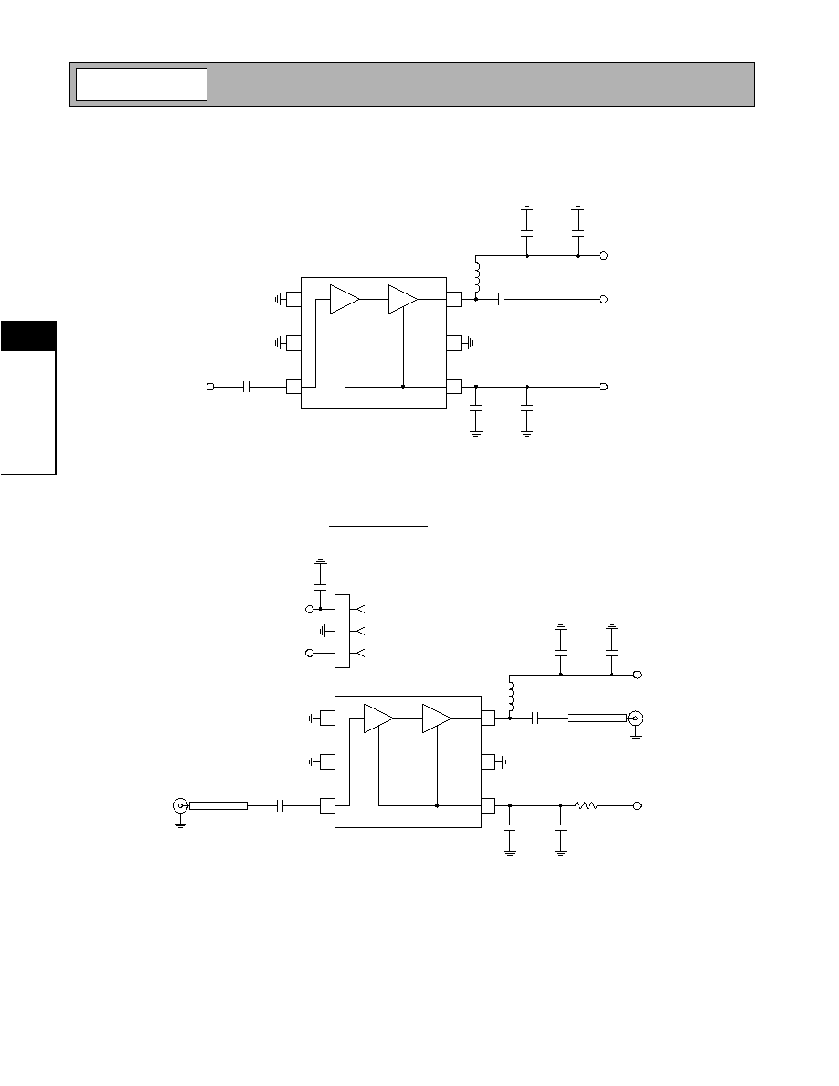
Application Schematic:
~1880 MHz Operation
Evaluation Board Schematic
(Download Bill of Materials from www.rfmd.com.)
1
2
3
6
4
5
6 pF
220 pF
10 nF
PD
1 pF
4.7 nH
VCC
10 nF
220 pF
RF IN
RF OUT
C3
6 pF
50
µ
strip
J1
RF IN
C2
220 pF
C1
10 nF
R1
0
PD
C4
1 pF
50
µ
strip
J2
RF OUT
L1
4.7 nH
VCC
C6
10 nF
C5
220 pF
2367400-
1
2
3
C7
4.7
µ
F
1
2
3
6
4
5
P1-1
VCC
GND
P1-3
PD

Preliminary
4-197
RF2367
Rev A1 010619
4
G
E
N
E
RA
L
P
URPO
SE
A
M
P
L
IF
IE
RS
Evaluation Board Layout
Board Size 0.948" x 1.063"
Board Thickness 0.031", Board Material FR-4

Preliminary
4-198
RF2367
Rev A1 010619
4
G
E
N
E
RA
L
P
URPO
SE
A
M
P
L
IF
IE
RS
Gain versus V
CC
V
PD
= 2.8 V, Frequency = 1880 MHz
19.5
20.0
20.5
21.0
21.5
22.0
22.5
23.0
2.5
3.0
3.5
4.0
4.5
5.0
5.5
6.0
V
CC
(V)
Gain
(dB)
Gain, -30∫
Gain, 25∫
Gain, 85∫
OIP3 versus V
CC
V
PD
= 2.8 V, Frequency = 1880 MHz
25.0
26.0
27.0
28.0
29.0
30.0
31.0
2.5
3.0
3.5
4.0
4.5
5.0
5.5
6.0
V
CC
(V)
OIP3
(dBm)
OIP3, -30∫
OIP3, 25∫
OIP3, 85∫
Noise Figure versus V
CC
V
PD
= 2.8 V, Frequency = 1880 MHz
1.5
2.0
2.5
3.0
3.5
2.5
3.0
3.5
4.0
4.5
5.0
5.5
6.0
V
CC
(V)
Noise
Figure
(
dB)
NF, -30∫
NF, 25∫
NF, 85∫
Output P1dB versus V
CC
V
PD
= 2.8 V, Frequency = 1880 MHz
10.0
11.0
12.0
13.0
14.0
15.0
16.0
17.0
2.5
3.0
3.5
4.0
4.5
5.0
5.5
6.0
V
CC
(V)
Output
P1dB
(dBm)
OP1dB, -30∫
OP1dB, 25∫
OP1dB, 85∫
I
CC
versus V
CC
V
PD
= 2.8 V, Frequency = 1880 MHz
25.0
27.0
29.0
31.0
33.0
35.0
37.0
39.0
41.0
43.0
2.5
3.0
3.5
4.0
4.5
5.0
5.5
6.0
V
CC
(V)
I
CC
(mA)
Icc+Ipd, -30∫
Icc+Ipd, 25∫
Icc+Ipd, 85∫
Gain versus V
PD
V
CC
= 3.0 V, Frequency = 1880MHz
20.5
21.0
21.5
22.0
22.5
23.0
2.70
2.75
2.80
2.85
2.90
V
PD
(V)
Gain
(dB)
Gain, -30∫
Gain, 25∫
Gain, 85∫

Preliminary
4-199
RF2367
Rev A1 010619
4
G
E
N
E
RA
L
P
URPO
SE
A
M
P
L
IF
IE
RS
OIP3 versus V
PD
V
CC
= 3.0 V, Frequency = 1880 MHz
25.50
26.00
26.50
27.00
27.50
28.00
28.50
29.00
29.50
30.00
30.50
2.70
2.75
2.80
2.85
2.90
V
PD
(V)
OIP3
(dBm)
OIP3, -30∫
OIP3, 25∫
OIP3, 85∫
Noise Figure versus V
PD
V
CC
= 3.0 V, Frequency = 1880 MHz
1.00
1.50
2.00
2.50
3.00
3.50
2.70
2.75
2.80
2.85
2.90
V
PD
(V)
Noise
Figure
(
dB)
NF, -30∫
NF, 25∫
NF, 85∫
Output P1dB versus V
PD
V
CC
= 3.0 V, Frequency = 1880 MHz
12.60
12.80
13.00
13.20
13.40
13.60
13.80
14.00
14.20
2.70
2.75
2.80
2.85
2.90
V
PD
(V)
Output
P1dB
(dBm)
OP1dB, -30∫
OP1dB, 25∫
OP1dB, 85∫
I
PD
versus V
PD
V
CC
= 3.0 V, Frequency = 1880 MHz
8.20
8.40
8.60
8.80
9.00
9.20
9.40
9.60
9.80
10.00
10.20
2.70
2.75
2.80
2.85
2.90
V
PD
(V)
I
PD
(mA)
Ipd, -30∫
Ipd, 25∫
Ipd, 85∫
Gain versus Frequency
V
CC
= 3.0 V, V
PD
= 2.8 V
20.0
20.5
21.0
21.5
22.0
22.5
23.0
1850.0
1860.0
1870.0
1880.0
1890.0
1900.0
1910.0
Frequency (MHz)
Gain
(dB)
Gain, -30∫
Gain, 25∫
Gain, 85∫
Input Impedance versus Frequency
V
CC
= 3.0 V, V
PD
= 2.8 V
1.75
1.80
1.85
1.90
1.95
2.00
2.05
2.10
1850.00
1860.00
1870.00
1880.00
1890.00
1900.00
1910.00
Frequency (MHz)
Input
VSWR
S11, -30∫
S11, 25∫
S11, 85∫

Preliminary
4-200
RF2367
Rev A1 010619
4
G
E
N
E
RA
L
P
URPO
SE
A
M
P
L
IF
IE
RS
Output Impedance versus Frequency
V
CC
= 3.0 V, V
PD
= 2.8 V
1.70
1.75
1.80
1.85
1.90
1.95
2.00
2.05
1850.00
1860.00
1870.00
1880.00
1890.00
1900.00
1910.00
Frequency (MHz)
Output
VSWR
S22, -30∫
S22, 25∫
S22, 85∫