
4-1
Product Description
Ordering Information
Typical Applications
Features
Functional Block Diagram
RF Micro Devices, Inc.
7628 Thorndike Road
Greensboro, NC 27409, USA
Tel (336) 664 1233
Fax (336) 664 0454
http://www.rfmd.com
Optimum Technology MatchingÆ Applied
Si BJT
GaAs MESFET
GaAs HBT
Si Bi-CMOS
SiGe HBT
Si CMOS
InGaP/HBT
GaN HEMT
SiGe Bi-CMOS
2
GND1
3
BIAS
4 RF OUT
1
RF IN
GND2
5
RF2373
3V LOW NOISE AMPLIFIER/
3V DRIVER AMPLIFIER
∑ WLAN LNA/Driver
∑ GPS LNA
∑ CDMA PCS LNA
∑ Low Noise Transmit Power Amplifier
∑ General Purpose Amplification
∑ Driver Amplifier for TX Power Amplifier
The RF2373 is a low noise amplifier with a very high
dynamic range designed for WLAN and digital cellular
applications. The device functions as an outstanding front
end low noise amplifier or driver amplifier in the transmit
chain of digital subscriber units where low transmit noise
power is a concern. When used as an LNA, the bias cur-
rent can be set externally. When used as a PA driver, the
IC can operate directly from a single cell Li-ion battery
and includes a power down feature that can be used to
completely turn off the device. The IC is featured in a
standard SOT 5-lead plastic package.
∑ Low Noise and High Intercept Point
∑ Adjustable Bias Current
∑ Power Down Control
∑ Single 1.8V to 6.0V Power Supply
∑ 400MHz to 3GHz Operation
∑ Extremely Small SOT 5-Lead Package
RF2373
3V Low Noise Amplifier/ 3V Driver Amplifier
RF2373PCK-414 Fully Assembled Evaluation Board with 5 Sample
Parts
0
Rev A1 040921
1
1.60
+ 0.01
0.400
2.80
+ 0.20
2.90
+ 0.10
0.45
+ 0.10
3∞ MAX
0∞ MIN
0.127
0.15
0.05
1.44
1.04
Dimensions in mm.
0.950
Package Style: SOT 5-Lead
Preliminary

Preliminary
4-2
RF2373
Rev A1 040921
Absolute Maximum Ratings
Parameter
Rating
Unit
Supply Voltage
-0.5 to +6.0
V
DC
Bias Voltage, V
BIAS
<V
CC
V
DC
Input RF Level
+15 (see note)
dBm
Current Drain, I
CC
32
mA
Operating Ambient Temperature
-40 to +85
∞C
Storage Temperature
-40 to +150
∞C
NOTE: Exceeding any one or a combination of the above maximum rating
limits may cause permanent damage. Input RF transients to +15dBm will
not harm the device. For sustained operation at inputs >+10dBm, a small
dropping resistor of 10
is recommended in series with the V
CC
.
Parameter
Specification
Unit
Condition
Min.
Typ.
Max.
Overall
25∞C, V
CC
=3.3V, at typical frequencies
unless otherwise specified
Supply Voltage (V
CC
)
2.7
3.3
5.0
V
Bias Voltage (V
BIAS
)
2.7
3.3
5.0
V
RF Frequency Range
800 to 2500
MHz
Power Down Current
10
µ
A
V
BIAS
=0V
Isolation
23
dB
Current Drain
(LNA)
8
14
19
mA
(Driver)
12
18
23
mA
IP2
55
dBm
Cellular Low Noise
Amplifier
Frequency
820
880
960
MHz
Gain
19.5
21.5
23.5
dB
I
CC
=10mA
Noise Figure
1.1
1.3
dB
IIP3
-3
-1
dBm
IP1dB
-13
-11
dBm
Input VSWR
2.0
2.5
Output VSWR
4.0
4.5
GPS Low Noise Amplifier
Frequency
1575
MHz
Gain
17.0
19.0
21.0
dB
I
CC
=10mA
Noise Figure
1.1
1.3
dB
IIP3
3
5
dBm
IP1dB
-7
-5
dBm
Input VSWR
1.7
2.2
Output VSWR
1.6
2.1
PCS Low Noise Amplifier
Frequency Range
1850
1920
1990
MHz
Gain
16.0
18.0
20.0
dB
I
CC
=10mA
Noise Figure
1.2
1.4
dB
IIP3
4
6
dBm
IP1dB
-7
-5
dBm
Input VSWR
1.8
2.3
Output VSWR
1.6
2.1
Caution! ESD sensitive device.
RF Micro Devices believes the furnished information is correct and accurate
at the time of this printing. However, RF Micro Devices reserves the right to
make changes to its products without notice. RF Micro Devices does not
assume responsibility for the use of the described product(s).

Preliminary
4-3
RF2373
Rev A1 040921
Parameter
Specification
Unit
Condition
Min.
Typ.
Max.
W-CDMA Low Noise
Amplifier
Frequency Range
1920
2045
2170
MHz
Gain
15.5
17.5
19.5
dB
I
CC
=10mA
Noise Figure
1.2
1.4
dB
IIP3
6
8
dBm
IP1dB
-3
-1
dBm
Input VSWR
1.8
2.3
Output VSWR
1.6
2.1
WLAN Low Noise
Amplifier
Frequency
2400
2450
2500
MHz
Gain
13.0
15.0
17.0
dB
I
CC
=10mA
Noise Figure
1.3
1.5
dB
IIP3
7.5
9.5
dBm
P1dB
-5.5
-3.5
dBm
Input VSWR
1.7
2.2
Output VSWR
1.1
1.6
Cellular Driver
Frequency
820
880
960
MHz
Gain
20.0
22.0
24.0
dB
I
CC
=18mA
Noise Figure
1.2
1.4
dB
OIP3
19
21
dBm
OP1dB
9
11
dBm
Input VSWR
2.0
2.5
Output VSWR
4.0
4.5
PCS Driver
Frequency Range
1850
1920
1990
MHz
Gain
16.5
18.5
20.5
dB
I
CC
=18mA
Noise Figure
1.3
1.5
dB
OIP3
21.5
23.5
dBm
OP1dB
10.5
12.5
dBm
Input VSWR
1.8
2.3
Output VSWR
1.6
2.1
W-CDMA Driver
Frequency Range
1920
2045
2170
MHz
Gain
15.0
17.5
20.0
dB
I
CC
=18mA
Noise Figure
1.3
1.5
dB
OIP3
23.5
25.5
dBm
OP1dB
14.5
16.5
dBm
Input VSWR
1.8
2.3
Output VSWR
1.6
2.1
WLAN Driver
Frequency
2400
2450
2500
MHz
Gain
13.5
15.5
17.5
dB
I
CC
=18mA
Noise Figure
1.4
1.6
dB
OIP3
23
25
dBm
OP1dB
10
12
dBm
Input VSWR
1.7
2.2
Output VSWR
1.1
1.6
Preliminary
4-4
RF2373
Rev A1 040921
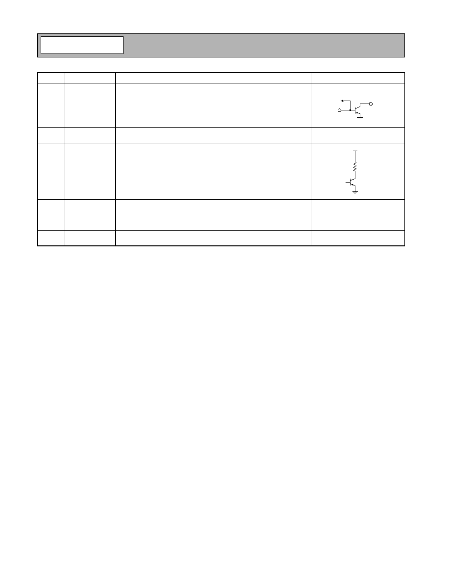
Pin
Function
Description
Interface Schematic
1
RF IN
RF input pin. This pin is DC coupled.
2
GND1
Ground connection. For best performance, keep traces physically short
and connect immediately to ground plane.
3
BIAS
This pin is used to control the bias current. An external resistor can be
used to set the bias current for any V
BIAS
voltage. See table with evalu-
ation board schematic.
4
RF OUT
Amplifier output pin. This pin is an open-collector output. It must be
biased to V
CC
through a choke or matching inductor. This pin is typi-
cally matched to 50
with a shunt bias/matching inductor and series
blocking/matching capacitor. Refer to application schematics.
5
GND2
Ground connection. For best performance, keep traces physically short
and connect immediately to ground plane.
RF IN
RF OUT
To Bias
Circuit
VBIAS
Preliminary
4-5
RF2373
Rev A1 040921
Evaluation Board Schematic
2
3
4
1
5
C2
100 pF
R1*
C3
Do Not
Place
VPD
LNA IN
* Refer to table for the values
L1*
C7*
V
CC
LNA OUT
C4
100 pF
C5
10 nF
P1
1
2
3
HDR_3
P1-1
VPD
GND
P1-3
VCC
C6*
C1
0.5 pF
L1 (nH)
2.7
2.7
C6 (pF)
1.5
0.5
Component
GPS
1575 MHz
PCS
1950 MHz
C7 (pF)
1.2
1.0
3.9
4.3
Cellular
900 MHz
2.0
2.7
DNP
W-CDMA
2140 MHz
1.0
2.2
DNP
WLAN
2450 MHz
1.0
2.7
3.0
V
PD
3.3
12
16
I
CC
R1 = 300
20
9
12
I
CC
R1 = 430
15
7
9
I
CC
R1 = 560
11
5
6
I
CC
R1 = 1 k
7
I
CC
R1 = 1.5 k
4
5
5
3.6
4.0
4.5
25
31
Over Limit
19
24
31
14
18
23
8
10
13
6
7
8
5.0
Over Limit
Over Limit
29
16
10
Note: V
CC
set to 3.3 V. I
CC
only slightly dependent on V
CC
.

Preliminary
4-6
RF2373
Rev A1 040921
This information pertains to the following charts.
Test condition unless otherwise specified: V
CC
=3.3V, use evaluation board for corresponding frequencies.
Collector Current versus V
BIAS
(R1 = 560 ohms)
0.0
5.0
10.0
15.0
20.0
25.0
30.0
35.0
0.0
0.5
1.0
1.5
2.0
2.5
3.0
3.5
4.0
4.5
5.0
V
BIAS
(V)
I
C
(m
A
)
-40∞C
+25∞C
+85∞C

Preliminary
4-7
RF2373
Rev A1 040921
Noise Figure versus Collector Current
LNA 880 MHz
0.0
0.2
0.4
0.6
0.8
1.0
1.2
1.4
1.6
1.8
0.0
5.0
10.0
15.0
20.0
25.0
30.0
I
C
(mA)
N
o
i
s
e
F
i
g
u
re
(d
B
)
-40∞C
+25∞C
+85∞C
Gain versus Collector Current
LNA 880 MHz
21.5
22.0
22.5
23.0
23.5
24.0
24.5
25.0
0.0
5.0
10.0
15.0
20.0
25.0
30.0
I
C
(mA)
G
a
in
(d
B
)
-40∞C
+25∞C
+85∞C
Noise Figure versus Collector Current
1575 MHz
0.0
0.2
0.4
0.6
0.8
1.0
1.2
1.4
1.6
1.8
0.0
5.0
10.0
15.0
20.0
25.0
30.0
I
C
(mA)
N
o
i
s
e
F
i
g
u
re
(d
B
)
-40∞C
+25∞C
+85∞C
Gain versus Collector Current
1575 MHz
16.5
17.0
17.5
18.0
18.5
19.0
19.5
20.0
20.5
0.0
5.0
10.0
15.0
20.0
25.0
30.0
I
C
(mA)
G
a
in
(d
B
)
-40∞C
+25∞C
+85∞C
Noise Figure versus Collector Current
1920 MHz
0.0
0.2
0.4
0.6
0.8
1.0
1.2
1.4
1.6
1.8
0.0
5.0
10.0
15.0
20.0
25.0
30.0
I
C
(mA)
N
o
i
s
e
F
i
g
u
re
(d
B
)
-40∞C
+25∞C
+85∞C
Gain versus Collector Current
1920 MHz
15.5
16.0
16.5
17.0
17.5
18.0
18.5
19.0
0.0
5.0
10.0
15.0
20.0
25.0
30.0
I
C
(mA)
G
a
in
(d
B
)
-40∞C
+25∞C
+85∞C

Preliminary
4-8
RF2373
Rev A1 040921
Noise Figure versus Collector Current
2025 MHz
0.0
0.2
0.4
0.6
0.8
1.0
1.2
1.4
1.6
1.8
0.0
5.0
10.0
15.0
20.0
25.0
30.0
I
C
(mA)
N
o
i
s
e
F
i
g
u
re
(d
B
)
-40∞C
+25∞C
+85∞C
Gain versus Collector Current
2025 MHz
16.0
16.5
17.0
17.5
18.0
18.5
19.0
19.5
0.0
5.0
10.0
15.0
20.0
25.0
30.0
I
C
(mA)
G
a
in
(d
B
)
-40∞C
+25∞C
+85∞C
Noise Figure versus Collector Current
2450 MHz
0.0
0.2
0.4
0.6
0.8
1.0
1.2
1.4
1.6
1.8
2.0
0.0
5.0
10.0
15.0
20.0
25.0
30.0
I
C
(mA)
N
o
i
s
e
F
i
g
u
re
(d
B
)
-40∞C
+25∞C
+85∞C
Gain versus Collector Current
2450 MHz
13.0
13.5
14.0
14.5
15.0
15.5
16.0
16.5
17.0
17.5
0.0
5.0
10.0
15.0
20.0
25.0
30.0
I
C
(mA)
G
a
in
(d
B
)
-40∞C
+25∞C
+85∞C