
¸
4-199
4
GEN
E
RA
L
P
URPO
S
E
A
M
P
L
IF
IE
RS
Preliminary
Product Description
Ordering Information
Typical Applications
Features
Functional Block Diagram
RF Micro Devices, Inc.
7628 Thorndike Road
Greensboro, NC 27409, USA
Tel (336) 664 1233
Fax (336) 664 0454
http://www.rfmd.com
Optimum Technology MatchingÆ Applied
Si BJT
GaAs MESFET
GaAs HBT
Si Bi-CMOS
SiGe HBT
Si CMOS
HB
G
N
D2
VC
C1
HB
HB
G
N
D1
HB IN
HB BIAS
LB
OUT
LB
GN
D
LB
I
N
HB OUT
LB SELECT
10
11
12
1
3
2
6
5
4
9
8
7
LB BIAS
HB SELECT
Logic
Control
RF2416
DUAL-BAND 2.7V LOW NOISE AMPLIFIER
∑ GSM/DCS Dual-Band Handsets
∑ Cellular/PCS Dual-Band Handsets
∑ General Purpose Amplification
∑ Commercial and Consumer Systems
The RF2416 is a dual-band low noise amplifier with
bypass switch designed for use as a front-end for
950MHz GSM and DCS1800/PCS1900 applications. It
may also be used for dual-band cellular/PCS application.
The 900MHz LNA is a single-stage amplifier with bypass
switch; the 1800/1900 LNA is a two-stage amplifier with
bypass switch. Both amplifiers have excellent noise figure
and high linearity in both high gain and bypass/low gain
mode. The device is packaged in a 3mmx3 mm, 12 pin,
leadless chip carrier.
∑ Low Noise and High Intercept Point
∑ Dual-Band Application GSM900 and
DCS1800/PCS1900
∑ Power Down Control
∑ Switchable Gain
RF2416
Dual-Band 2.7V Low Noise Amplifier
RF2416 PCBA
Fully Assembled Evaluation Board
4
Rev A2 010810
Dimensions in mm.
12∞
max
1.00
0.85
3.00
sq.
1.25
0.95
sq.
2
0.30
0.18
0.50
0.23
0.13
4 PLCS
0.80
0.65
NOTES:
Shaded Pin is Lead 1.
1
Dimension applies to plated terminal and is measured between 0.02 mm and
0.25 mm from terminal end.
2
5
Die thickness allowable: 0.305 mm max.
Package Warpage: 0.05 mm max.
4
Pin 1 identifier must exist on top surface of package by identification mark or
feature on the package body. Exact shape and size is optional.
3
0.65
0.30
4 PLCS
0.60
0.24 typ
0.75
0.50
0.05
0.01
Package Style: LCC, 12-Pin, 3x3

Preliminary
4-200
RF2416
Rev A2 010810
4
GEN
E
RA
L
P
URPO
S
E
A
M
P
L
IF
IE
RS
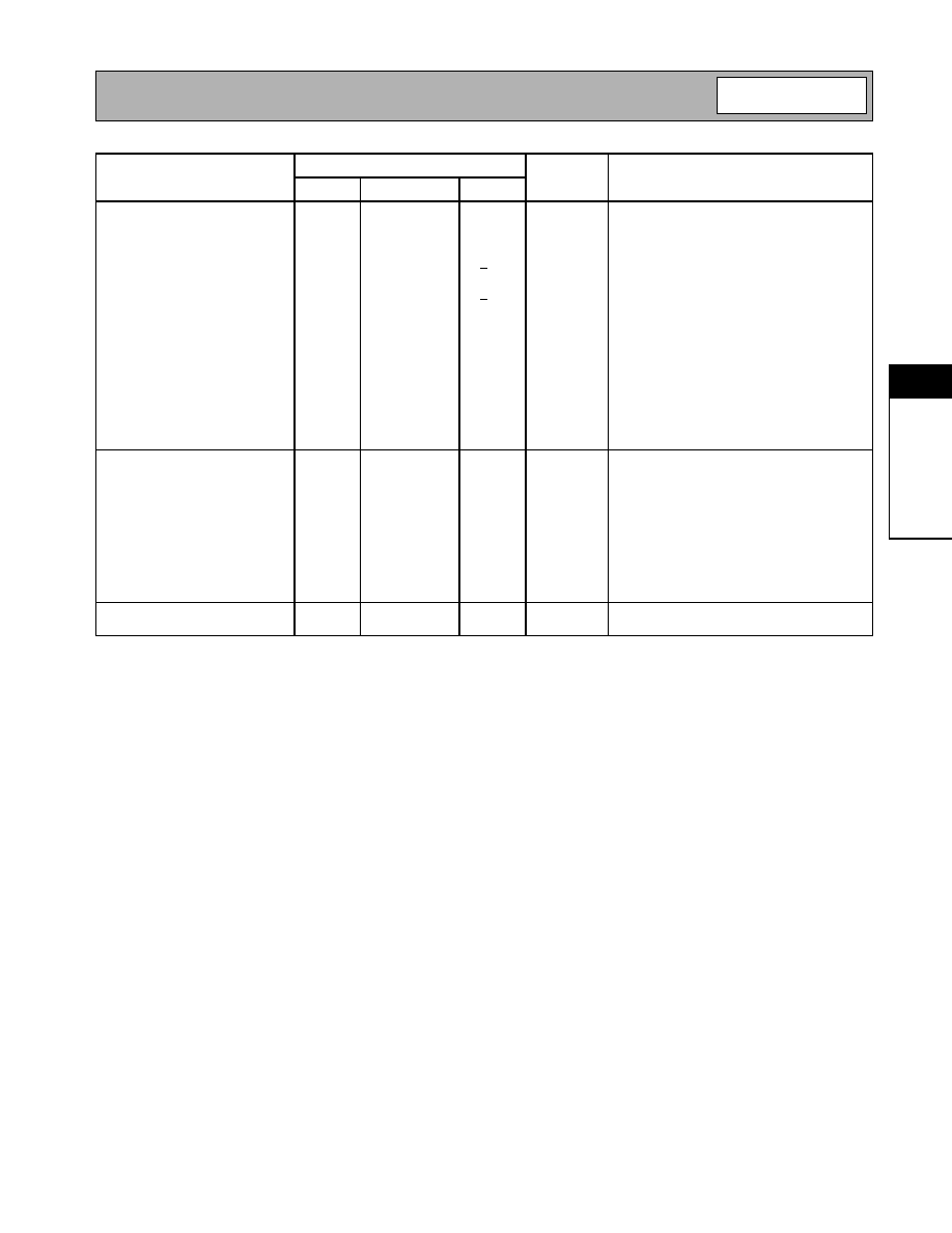
Absolute Maximum Ratings
Parameter
Rating
Unit
Supply Voltage
-0.5 to +6.0
V
DC
Input RF Level
+10
dBm
Storage Temperature
-40 to +150
∞C
Parameter
Specification
Unit
Condition
Min.
Typ.
Max.
Operating Range
Overall Frequency Range
800
1000
MHz
Low Band Operation
1800
2000
MHz
High Band Operation
Supply Voltage (V
CC
)
2.7
2.8
3.0
V
VCC1 HB, VCC2 HB, VCC1 LB
Power Down Voltage (V
BIAS
)
2.7
2.8
3.0
V
HB BIAS, LB BIAS
Logic Control Voltage Level
0
3.0
V
HB SELECT, LB SELECT
Operating Ambient Temperature
-40
+85
o
C
Input Impedance
50
Output Impedance
50
950MHz Performance -
High Gain Mode
T = 25∞C, RF = 950MHz,
VCC1LB= VCC2LB = 2.78V, LBSelect= 0V,
Z
IN
=Z
O
= 50
Gain
14
15.5
17
dB
Gain Variation Over
Temperature Range
+0.5
dB
Gain Variation Over
Frequency Band
+0.5
dB
Noise Figure
1.1
2.0
dB
Reverse Isolation
15
21
dB
Input IP3
+2.0
+5.0
dBm
Input P1dB
-12
-9
dB
Input VSWR
2:1
Output VSWR
2:1
Total Current Draw
4.8
6.0
mA
900MHz LNA ENABLED, 1900MHz LNA
DISABLED. I
CC
+ I
PD
950MHz Performance -
Bypass Mode
T = 25∞C, RF = 950MHz,
VCC1LB = VCC2LB=2.78V, LBSelect= 2.7V,
Z
IN
=Z
O
= 50
Gain
-8
-6
-3
dB
Gain Reduction
21.5
dBc
Input IP3
12.0
15.0
dBm
Input P1dB
-1
+2
dB
Input VSWR
2.5:1
Output VSWR
2:1
Total Current Draw
See Application Notes
Caution! ESD sensitive device.
RF Micro Devices believes the furnished information is correct and accurate
at the time of this printing. However, RF Micro Devices reserves the right to
make changes to its products without notice. RF Micro Devices does not
assume responsibility for the use of the described product(s).
Preliminary
4-201
RF2416
Rev A2 010810
4
GEN
E
RA
L
P
URPO
S
E
A
M
P
L
IF
IE
RS
Parameter
Specification
Unit
Condition
Min.
Typ.
Max.
1850MHz Performance -
High Gain Mode
T = 25∞C, RF =1850MHz, VCC1HB = 2.78V,
HB Select= 0V, Z
IN
=Z
O
= 50
Gain
15
17.5
19
dB
Gain Variation Over
Temperature Range
+0.5
dB
Gain Variation Over
Frequency Band
+0.5
dB
Noise Figure
1.5
2.1
dB
Reverse Isolation
15
20
dB
Input IP3
-2.0
+1.0
dBm
Input P1dB
-13
-10
dB
Input VSWR
2:1
Output VSWR
2:1
Total Current Draw
8.2
10
mA
1900MHz LNA ENABLED, 900MHz LNA
DISABLED. I
CC
+ I
PD
1850MHz Performance -
Bypass Mode
T = 25∞C, RF =1850MHz, VCC1HB = 2.78V,
HB Select= 2.7V, Z
IN
=Z
O
= 50
Gain
-7
-5
-3
dB
Gain Reduction
22
23
24
dBc
Input IP3
12.0
15.0
dBm
Input P1dB
+5
+8
dB
Input VSWR
2:1
Output VSWR
2.5:1
Total Current Draw
See Applications Notes
AGC Settling Time
10
µ
s
Rise and Fall Time
10
µ
s

Preliminary
4-202
RF2416
Rev A2 010810
4
GEN
E
RA
L
P
URPO
S
E
A
M
P
L
IF
IE
RS
Pin
Function
Description
Interface Schematic
1
HB IN
DCS1800/PCS1900 RF input pin.
2
HB BIAS
HB BIAS is set to the supply voltage at high gain mode. For bypass
mode see "Gain Select Possibility".
3
LB BIAS
LB BIAS is set to the supply voltage at high gain mode. For bypass
mode see "Gain Select Possibility".
4
LB IN
GSM900 RF input pin.
5
LB GND
LNA emittance inductance. Total inductance is comprised of
package+bondwire+ L2 on PCB.
6
LB OUT
GSM900 Amplifier Output pin. This pin is an open-collector output. It
must be biased to V
CC
through a choke or matching inductor. This pin
is typically matched to 50
with a shunt bias/matching inductor and
series blocking/matching capacitor. Refer to application schematics.
7
LB SELECT
This pin selects high gain and bypass for GSM900.
Select < 0.8V, high gain.
Select > 1.8V, low gain.
8
HB SELECT
This pin selects high gain and bypass for DCS1800/PCS1900.
Select < 0.8V, high gain.
Select > 1.8V, low gain.
9
HB OUT
DCS1800 Amplifier Output pin. This pin is an open-collector output. It
must be biased to V
CC
through a choke or matching inductor. This pin
is typically matched to 50
with a shunt bias/matching inductor and
series blocking/matching capacitor. Refer to application schematics.
HB IN
VCC1 HB
To Bias
Circuit
HB GND1
HB VREF/P
LB VREF/PD
LB OUT
LB GND
LB IN
To Bias
Circuit
LB SELECT
HB SELECT
HB OUT
HB GND2

Preliminary
4-203
RF2416
Rev A2 010810
4
GEN
E
RA
L
P
URPO
S
E
A
M
P
L
IF
IE
RS
Pin
Function
Description
Interface Schematic
10
HB GND2
LNA2 emittance inductance. Total inductance is comprised of
package+bondwire+L5 on PCB.
11
VCC1 HB
Open collector for first stage LNA of DCS1800/PCS1900. It must be
biased to V
CC
through a choke or matching inductor.
12
HB GND1
LNA1 emittance inductance. Total inductance is comprised of
package+bondwire+L7 on PCB.
VCC1 HB
HB GND1

Preliminary
4-204
RF2416
Rev A2 010810
4
GEN
E
RA
L
P
URPO
S
E
A
M
P
L
IF
IE
RS
Application Notes
Bypass Mode Configurations
The RF2416 may be placed into either high gain or bypass mode via the HB SELECT and LB SELECT pins for high
band and low band operation, respectively. The high gain state is selected by asserting the select pin for the appropriate
band to a voltage level of less than 0.8V. For Bypass operation, there are two possible methods for placing the RF2416
into this low gain state. The table below shows the two possible Bypass states for each mode.
RF2416 Bypass Mode Possibilities
For both Bypass configurations, the select pin for the appropriate band must be placed at a level greater than or equal to
1.8 V. The difference between the Bypass possibilities is determined by the specific application's ability to change the
voltage of the bias pins independently of V
CC
. The advantage of the ability to assert the bias pins to 0V when in Bypass
mode is shown by the decreased current draw when in this Bypass configuration.
Gain Select
(HB Mode)
HB BIAS (V)
VCC1_HB and
VCC2_HB (V)
Current (mA)
2.7
0
2.78
1.4
2.7
2.7
2.78
1.9
Gain Select
(LB Mode)
LB BIAS (V)
VCC1_LB (V)
Current (mA)
2.7
0
2.78
0.8
2.7
2.7
2.78
1.5

Preliminary
4-205
RF2416
Rev A2 010810
4
GEN
E
RA
L
P
URPO
S
E
A
M
P
L
IF
IE
RS
Evaluation Board Schematic
(Download Bill of Materials from www.rfmd.com.)
10
11
12
1
3
2
6
5
4
9
8
7
Logic
Control
C1
33 nF
50
µ
strip
J1
HB IN
R1
0
C2
0.1
µ
F
HB BIAS
C3
0.1
µ
F
LB BIAS
L2
6.8 nH
C4
33 nF
50
µ
strip
J2
LB IN
C7
2.0 pF
50
µ
strip
J3
LB OUT
VCC1 LB
C8
0.1
µ
F
LB SELECT
C9
0.1
µ
F
HB SELECT
L4
3.3 nH
C10
0.7 pF
50
µ
strip
J4
HB OUT
VCC1 HB
L5
1.0 nH
VCC1 HB
L7
1.0 nH
R2
0
L1
47 nH
50
µ
strip
R3
0
L6
3.3 nH
C13
0.1
µ
F
C14
100 pF
2416310, rev. 3
L3
8.2 nH
C5
0.1
µ
F
C6
100 pF
C11
0.1
µ
F
C12
100 pF
P2
1
2
3
CON3
P2-3
LB SELECT
GND
P2-1
HB SELECT
P1
1
2
3
CON3
P1-1
HB BIAS
GND
P1-3
LB BIAS
P3
1
2
3
CON3
GND
P3-3
VCC1 LB
P3-1
VCC1 HB

Preliminary
4-206
RF2416
Rev A2 010810
4
GEN
E
RA
L
P
URPO
S
E
A
M
P
L
IF
IE
RS
Evaluation Board Layout
Board Size 2" x 2"
Board Thickness 0.060", Board Material FR-4, Multi-Layer

Preliminary
4-207
RF2416
Rev A2 010810
4
GEN
E
RA
L
P
URPO
S
E
A
M
P
L
IF
IE
RS
0
1.
0
1.
0
-1
.
0
10.
0
10.0
-1
0.0
5.
0
5.0
-5
.0
2.
0
2.
0
-2
.0
3.
0
3.
0
-3
.0
4.
0
4.0
-4
.0
0.
2
0.2
-0.2
0.
4
0.
4
-0
.4
0.
6
0
.6
-0
.6
0.
8
0
.8
-0
.8
Low Band High Gain Mode (S22)
Swp Max
6GHz
Swp Min
0.01GHz
10 MHz
500 MHz
950 MHz
1.5 GHz
3.5 GHz
4.5 GHz
5 GHz
5.5 GHz
0
1.
0
1.
0
-1
.
0
10.
0
10.0
-1
0.0
5.
0
5.0
-5
.0
2.
0
2.
0
-2
.0
3.
0
3.
0
-3
.0
4.
0
4.0
-4
.0
0.
2
0.2
-0.2
0.
4
0.
4
-0
.4
0.
6
0
.6
-0
.6
0.
8
0
.8
-0
.8
Low Band Bypass Mode (S11)
Swp Max
6GHz
Swp Min
0.01GHz
10 MHz
950 MHz
3 GHz
4 GHz
4.5 GHz
5 GHz
0
1.
0
1.
0
-1
.
0
10.
0
10.0
-1
0.0
5.
0
5.0
-5
.0
2.
0
2.
0
-2
.0
3.
0
3.
0
-3
.0
4.
0
4.0
-4
.0
0.
2
0.2
-0.2
0.
4
0.
4
-0
.4
0.
6
0
.6
-0
.6
0.
8
0
.8
-0
.8
Low Band Bypass Mode (S22)
Swp Max
6GHz
Swp Min
0.01GHz
10 MHz
950 MHz
1.5 GHz
4 GHz
5.5 GHz
0
1.
0
1.
0
-1
.
0
10.
0
10.0
-1
0.0
5.
0
5.0
-5
.0
2.
0
2.
0
-2
.0
3.
0
3.
0
-3
.0
4.
0
4.0
-4
.0
0.
2
0.2
-0.2
0.
4
0.
4
-0
.4
0.
6
0
.6
-0
.6
0.
8
0
.8
-0
.8
Low Band High Gain Mode (S11)
Swp Max
6GHz
Swp Min
0.01GHz
5 GHz
4 GHz
3.5 GHz
3 GHz
2 GHz
950 MHz
500 MHz
10 MHz

Preliminary
4-208
RF2416
Rev A2 010810
4
GEN
E
RA
L
P
URPO
S
E
A
M
P
L
IF
IE
RS
S-Parameter Conditions:
All plots shown were taken at VCC =2.78V and Ambient Temperature=25∞C.
Note:
All S11 and S22 plots shown were taken from an RF2416 while on a 2416310 evaluation board. The data was captured without the exter-
nal input or output tuning components in place, and the reference point at the HB IN and HB OUT pins for high band and LB IN and LB
OUT for low band.
0
1.0
1.0
-1.0
10.0
10.0
-1
0.
0
5.0
5.
0
-5
.0
2.0
2
.
0
-
2
.
0
3.0
3.
0
-3
.0
4.0
4.
0
-4
.0
0.2
0.
2
-0
.2
0.4
0
.
4
-
0
.
4
0.6
0
.
6
-
0
.
6
0.8
0
.
8
-
0
.
8
High Band Bypass Mode (S22)
Swp Max
6GHz
Swp Min
0.01GHz
1850 MHz
4 GHz
1 GHz
10 MHz
4.5 GHz
0
1.
0
1.
0
-1
.
0
10.
0
10.0
-1
0.0
5.
0
5.0
-5
.0
2.
0
2.
0
-2
.0
3.
0
3.
0
-3
.0
4.
0
4.0
-4
.0
0.
2
0.2
-0.2
0.
4
0.
4
-0
.4
0.
6
0
.6
-0
.6
0.
8
0
.8
-0
.8
High Band Bypass Mode (S11)
Swp Max
6GHz
Swp Min
0.01GHz
1850 MHz
4 GHz
1.5 GHz
3 GHz
1 GHz
5 GHz
2 GHz
500 MHz
10 MHz
0
1.
0
1.
0
-1
.
0
10.
0
10.0
-1
0.0
5.
0
5.0
-5
.0
2.
0
2.
0
-2
.0
3.
0
3.
0
-3
.0
4.
0
4.0
-4
.0
0.
2
0.2
-0.2
0.
4
0.
4
-0
.4
0.
6
0
.6
-0
.6
0.
8
0
.8
-0
.8
High Band High Gain Mode (S11)
Swp Max
6GHz
Swp Min
0.01GHz
10 MHz
1850 MHz
500 MHz
2.5 GHz
3 GHz
4 GHz
1 GHz
1.5 GHz
2 GHz
0
1.
0
1.
0
-1
.
0
10.
0
10.0
-1
0.0
5.
0
5.0
-5
.0
2.
0
2.
0
-2
.0
3.
0
3.
0
-3
.0
4.
0
4.0
-4
.0
0.
2
0.2
-0.2
0.
4
0.
4
-0
.4
0.
6
0
.6
-0
.6
0.
8
0
.8
-0
.8
High Band High Gain Mode (S22)
Swp Max
6GHz
Swp Min
0.01GHz
4 GHz
4.5 GHz
10 MHz
1 GHz
1850 MHz
3.5 GHz