
8-35
8
F
R
O
N
T
-
E
NDS
Product Description
Ordering Information
Typical Applications
Features
Functional Block Diagram
RF Micro Devices, Inc.
7628 Thorndike Road
Greensboro, NC 27409, USA
Tel (336) 664 1233
Fax (336) 664 0454
http://www.rfmd.com
Optimum Technology MatchingÆ Applied
Si BJT
GaAs MESFET
GaAs HBT
Si Bi-CMOS
¸
SiGe HBT
Si CMOS
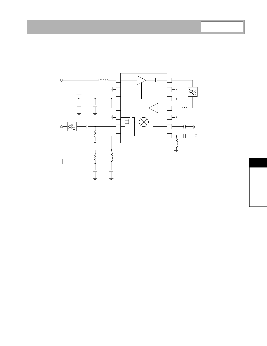
1
2
3
4
5
6
7
14
13
12
11
10
9
8
LNA IN
GND
VDD1
VDD2
IF BYP
IF2 OUT
IF1 OUT
LNA OUT
GND
GND
RF IN
GND
DEC
LO IN
LNA
MIXER
BUFFER
10pF
RF AMP
RF2418
LOW CURRENT LNA/MIXER
∑ UHF Digital and Analog Receivers
∑ Digital Communication Systems
∑ Spread-Spectrum Communication Systems
∑ Commercial and Consumer Systems
∑ 433MHz and 915MHz ISM Band Receivers
∑ General Purpose Frequency Conversion
The RF2418 is a monolithic integrated UHF receiver
front-end. The IC contains all of the required components
to implement the RF functions of the receiver except for
the passive filtering and LO generation. It contains an
LNA (low-noise amplifier), a second RF amplifier, a dual-
gate GaAs FET mixer, and an IF output buffer amplifier
which will drive a 50
load. In addition, the IF buffer
amplifier may be disabled and a high impedance output is
provided for easy matching to IF filters with high imped-
ances. The output of the LNA is made available as an
output to permit the insertion of a bandpass filter between
the LNA and the RF/Mixer section. The LNA section may
be disabled by removing the VDD1 connection to the IC.
∑ Single 3V to 6.5V Power Supply
∑ High Dynamic Range
∑ Low Current Drain
∑ High LO Isolation
∑ LNA Power Down Mode for Large Signals
RF2418
Low Current LNA/Mixer
RF2418 PCBA
Fully Assembled Evaluation Board
8
Rev A6 010717
0.156
0.148
0.059
0.057
0.252
0.236
0.010
0.004
.018
.014
8∞ MAX
0∞ MIN
0.0500
0.0164
0.010
0.007
0.347
0.339
0.050
Package Style: SOIC-14
8-36
RF2418
Rev A6 010717
8
F
R
O
N
T
-
E
NDS
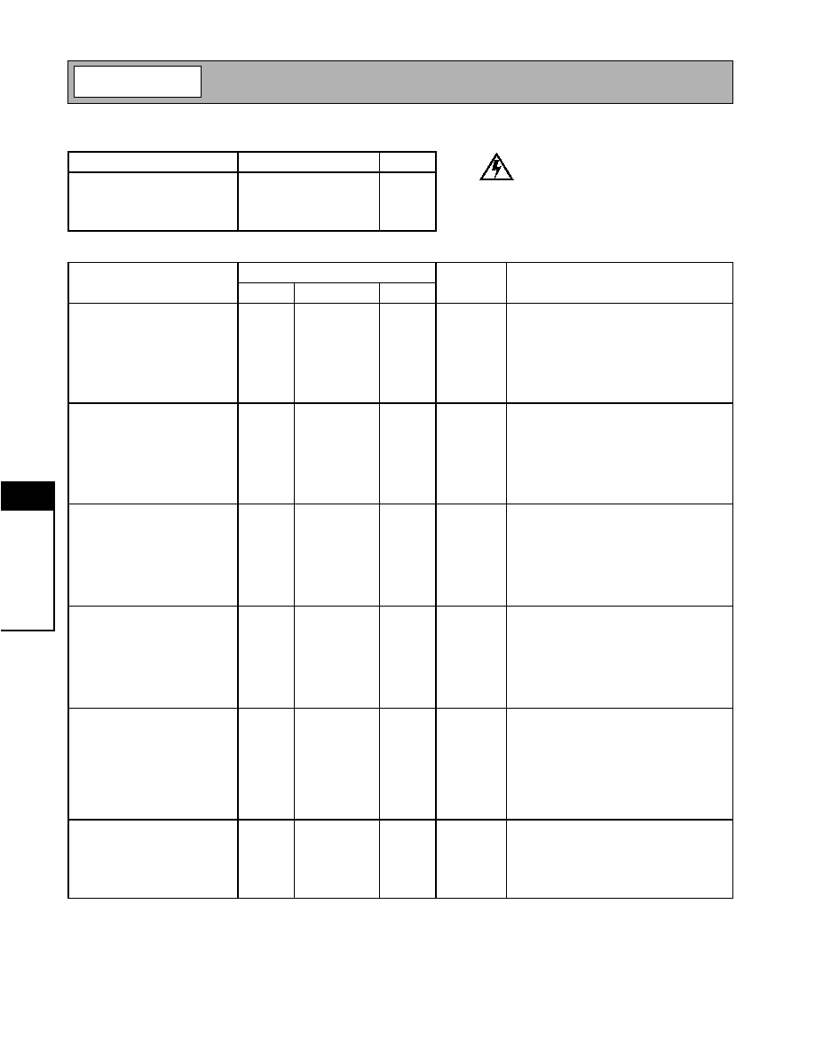
Absolute Maximum Ratings
Parameter
Rating
Unit
Supply Voltage
-0.5 to 7
V
DC
Input LO and RF Levels
+6
dBm
Ambient Operating Temperature
-40 to +85
∞C
Storage Temperature
-40 to +150
∞C
Parameter
Specification
Unit
Condition
Min.
Typ.
Max.
Overall
T = 25∞C, V
CC
=5V, RF =850MHz,
LO= 921MHz
RF Frequency Range
400 to 1100
MHz
Cascade Power Gain
23
dB
High impedance output
Cascade IP
3
-13
dBm
Referenced to the input
Cascade Noise Figure
2.4
dB
Single sideband, includes image filter with
1.0dB insertion loss
First Section (LNA)
Noise Figure
1.8
2.0
dB
Input VSWR
1.5:1
With external series matching inductor
Input IP3
+3.0
+4.0
dBm
Gain
13
14
dB
Reverse Isolation
40
dB
Output VSWR
1.5:1
Second Section (RF Amp,
Mixer, IF1)
High impedance output
Noise Figure
9.5
dB
Single Sideband
Input VSWR
1.5:1
With external series matching inductor
Input IP3
+1
dBm
Conversion Power Gain
7
9
dB
Output Impedance
4000||10pF
Open Collector
Second Section (RF Amp,
Mixer, IF2)
Buffered output, 50
load
Noise Figure
10
dB
Single Sideband
Input VSWR
1.5:1
With external series matching inductor
Input IP3
-0.5
0
dBm
Conversion Gain
5
6
dB
Output Impedance
30
LO Input
LO Frequency
300 to 1200
MHz
LO Level
-6 to +6
dBm
LO to RF Rejection
15
dB
LO to IF Rejection
40
dB
With pin 5 connected to ground.
LO Input VSWR
1.3:1
In order to achieve a low VSWR match at
this input, an 82
resistor to ground is
placed in parallel with this port.
Power Supply
Voltage
3.0
6.5
V
Current Consumption
14
mA
V
CC
= 5.0V, LNA On, Mixer On, Buffer Off
12
20
26
mA
V
CC
= 5.0V, LNA On, Mixer On, Buffer On
6
9
20
mA
V
CC
= 5.0V, LNA Off, Mixer On, Buffer Off
Caution! ESD sensitive device.
RF Micro Devices believes the furnished information is correct and accurate
at the time of this printing. However, RF Micro Devices reserves the right to
make changes to its products without notice. RF Micro Devices does not
assume responsibility for the use of the described product(s).

8-37
RF2418
Rev A6 010717
8
F
R
O
N
T
-
E
NDS
Pin
Function
Description
Interface Schematic
1
LNA IN
A series 10nH matching inductor is necessary to achieve specified gain
and noise figure at 900MHz. This pin is NOT internally DC-blocked. An
external blocking capacitor must be provided if the pin is connected to a
device with DC present. A DC path to ground (i.e. an inductor or resis-
tor to ground) is, however, acceptable at this pin. If a blocking capacitor
is required, a value of 22pF is recommended.
2
GND
Ground connection. Keep traces physically short and connect immedi-
ately to ground plane for best performance.
3
VDD1
Supply Voltage for the LNA only. A 22pF external bypass capacitor is
required and an additional 0.01
µ
F is required if no other low frequency
bypass capacitors are near by. The trace length between the pin and
the bypass capacitors should be minimized. The ground side of the
bypass capacitors should connect immediately to ground plane.
For large input signals, VDD1 may be disconnected, resulting in the
LNA's gain changing from +11dB to -26dB and current drain decreas-
ing by 4mA. If the LNA is never required for use, then this pin can be
left unconnected or grounded, and Pin 11 is used as the first input.
4
VDD2
Power supply for the IF buffer amplifier. If the high impedance mixer
output is being used, then this pin is not connected.
5
IF BYP
If this pin is connected to ground, an internal 10pF capacitor is con-
nected in parallel with the mixer output. This capacitor functions as an
LO trap, which reduces the amount of LO to IF bleed-through and pre-
vents high LO voltages at the mixer output from degrading the mixer's
dynamic range. At higher IF frequencies, this capacitance, along with
parasitic layout capacitance, should be parallel resonated out by the
choice of the bias inductor value at pin 7. If the internal capacitor is not
connected to ground, the buffer amplifier could become unstable. A
~10pF capacitor should be added at the output to maintain the buffer's
stability, but the gain will not be significantly affected.
6
IF2 OUT
50
buffered (open source) output port, one of two output options. Pin
7 must have a bias resistor to V
DD
and pin 6 must have a bias resistor
to ground (see Buffered Output Application Schematic) in order to turn
the buffer amplifier on. Current drain will increase by approximately
8mA at 5V, and by approximately 5mA at 3V. It is recommended that
these bias resistors be less than 1k
.
7
IF1 OUT
High impedance (open drain) output port, one of two output options.
This pin must be connected to V
DD
through a resistor or inductor in
order to bias the mixer, even when using IF2 Output. In addition, a
0.01
µ
F bypass capacitor is required at the other end of the bias resistor
or inductor. The ground side of the bypass capacitor should connect
immediately to ground plane. This output is intended to drive high
impedance IF filters. The recommended matching network is shunt L,
series C (see the application schematic, high impedance output). This
topology will provide matching, bias, and DC-blocking.
8
LO IN
Mixer LO input. A high-pass matching network, such as a single shunt
inductor (as shown in the application schematics), is the recommended
topology because it also rejects IF noise at the mixer input. This filtering
is required to achieve the specified noise figures. This pin is NOT inter-
nally DC-blocked. An external blocking capacitor must be provided if
the pin is connected to a device with DC present. A DC path to ground
(i.e. an inductor or resistor to ground) is, however, acceptable at this
pin. If a blocking capacitor is required, a value of 22pF is recom-
mended.
9
RF BYP
Connection for the external bypass capacitor for the mixer RF input
preamp. 1000pF is recommended. The trace length between the pin
and the capacitor should be minimized. The ground side of the bypass
capacitor should connect immediately to ground plane.
LNA IN
IF2 OUT
IF1 OUT
LO IN

8-38
RF2418
Rev A6 010717
8
F
R
O
N
T
-
E
NDS
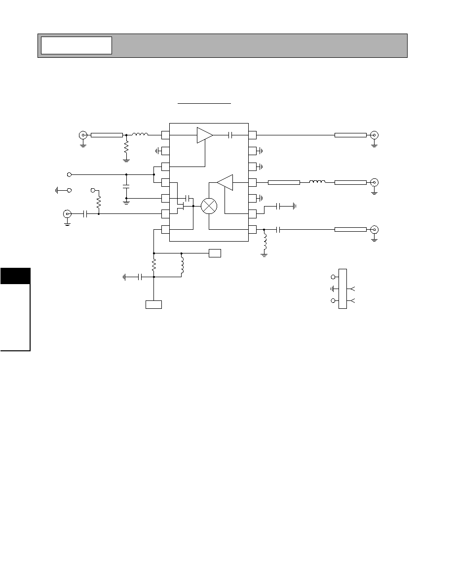
Application Schematic
High Impedance Output Configuration
850MHz
Pin
Function
Description
Interface Schematic
10
GND
Same as pin 2.
11
RF IN
Mixer RF Input port. For a 50
match at 900MHz use a 15nH series
inductor. This pin is NOT internally DC-blocked. An external blocking
capacitor must be provided if the pin is connected to a device with DC
present. A DC path to ground (i.e. an inductor or resistor to ground) is,
however, acceptable at this pin. If a blocking capacitor is required, a
value of 22pF is recommended.To minimize the mixer's noise figure, it
is recommended to have a RF bandpass filter before this input. This will
prevent the noise at the image frequency from being converted to the
IF.
12
GND
Same as pin 2.
13
GND
Same as pin 2.
14
LNA OUT
50
output. Internally DC-blocked.
RF IN
LNA OUT
1
2
3
4
5
6
7
14
13
12
11
10
9
8
LNA
MIXER
BUFFER
10pF
RF AMP
IF Filter, Hi Z
IF OUT
RF IN
Image Filter 50
10 nH
LO IN
V
DD
V
DD
L1 and C1 are picked to match the mixer's output impedance (4 k
II 10 pF) to the IF
filter's impedance, at the IF frequency. C1 also serves as a DC block, in case the IF filter
is not an open circuit at DC.
L1
100 nF
C1
47 pF
100 nF
10 nH
4 pF
1 nF
15 nH
8-39
RF2418
Rev A6 010717
8
F
R
O
N
T
-
E
NDS
Application Schematic
Buffered Output Configuration
850MHz
1
2
3
4
5
6
7
14
13
12
11
10
9
8
LNA
MIXER
BUFFER
10pF
RF AMP
IF Filter, 50
IF OUT
RF IN
Image Filter, 50
15nH
10 nH
LO IN
V
DD
V
DD
L1 should parallel resonate, at the IF frequency, with the internal
10pF capacitor plus any extra parasitic layout capacitance.
R1 and R2 are bias resistors that set the bias current for the buffer
amplifier. The value recommended is 510 W, each. Higher values
will decrease the current consumption but also decrease the output
level at which voltage clipping begins to occur. At lower IF
frequencies, where the internal 10 pF capacitor does not roll off the
conversion gain, L1 may be eliminated.
C1 is a blocking capacitor, in case the IF filter's input is not an open
circuit at DC.
10 nH
47 pF
100 nF
R1
C1
L1
R2
100 nF
100 nF
1 nF
4 pF
8-40
RF2418
Rev A6 010717
8
F
R
O
N
T
-
E
NDS
Evaluation Board Schematic
RF=850MHz, IF=71MHz
(Download Bill of Materials from www.rfmd.com.)
1
2
3
4
5
6
7
14
13
12
11
10
9
8
LNA
MIXER
BUFFER
10pF
RF AMP
L3
10 nH
C3
47 pF
C1
0.1
µ
F
L1
1
µ
H
L2
18 nH
C2
1 nF
R3
610
R1
300
E2
E1
L4
10 nH
R4
5.11 k
C4
0.1
µ
F
C5
3 pF to 5 pF
see note
Notes:
For high impedance output
1) Populate L1 and TP1
2) Remove jumper E1 to E2
50
µ
strip
50
µ
strip
50
µ
strip
2418400C
Jumper
TP1
see note
VDD
50
µ
strip
P1
1
2
3
NC
GND
P1-3
VDD
J1
LNA IN
50
µ
strip
J2
IF OUT
P1-3
J3
LO IN
J4
RF IN
J5
LNA OUT

8-41
RF2418
Rev A6 010717
8
F
R
O
N
T
-
E
NDS
Evaluation Board Layout
Board Size 1.52" x 1.52"
Board Thickness 0.031", Board Material FR-4

8-42
RF2418
Rev A6 010717
8
F
R
O
N
T
-
E
NDS
High Impedance Mixer Gain versus Voltage, RF=850MHz
7.0
7.5
8.0
8.5
9.0
9.5
10.0
3.0
3.5
4.0
4.5
5.0
5.5
6.0
6.5
Voltage (V)
Gain
(dB)
T =-40
T = 26
T = 85
High Impedance Casc. Gain versus Voltage,
RF=850MHz
14.0
16.0
18.0
20.0
22.0
24.0
26.0
3.0
3.5
4.0
4.5
5.0
5.5
6.0
6.5
Voltage (V)
Gain
(dB)
T =-40
T =26
T = 85
High Impedance Mixer Input IP3 versus Voltage,
RF=850MHz
0.5
1.0
1.5
2.0
2.5
3.0
3.5
4.0
3.0
3.5
4.0
4.5
5.0
5.5
6.0
6.5
Voltage (V)
IIP3
(dBm)
T =-40
T = 26
T = 85
High Impedance Casc. Input IP3 versus Voltage,
RF=850MHz
-15.0
-14.5
-14.0
-13.5
-13.0
-12.5
-12.0
-11.5
-11.0
-10.5
-10.0
3.0
3.5
4.0
4.5
5.0
5.5
6.0
6.5
Voltage (V)
IIP3
(dBm)
T =-40
T =26
T = 85
Buffered LNA Gain versus Voltage,
RF=850MHz
7.0
8.0
9.0
10.0
11.0
12.0
13.0
14.0
15.0
16.0
17.0
3.0
3.5
4.0
4.5
5.0
5.5
6.0
6.5
Voltage (V)
Gain
(dB)
T =-40
T = 26
T =85
Buffered Mixer Gain versus Voltage,
RF=850MHz
5.0
6.0
7.0
8.0
9.0
10.0
11.0
12.0
13.0
14.0
15.0
3.0
3.5
4.0
4.5
5.0
5.5
6.0
6.5
Voltage (V)
Gain
(dB)
T =-40
T = 26
T = 85

8-43
RF2418
Rev A6 010717
8
F
R
O
N
T
-
E
NDS
Buffered Casc. Gain versus Voltage,
RF=850MHz
5.0
10.0
15.0
20.0
25.0
30.0
3.0
3.5
4.0
4.5
5.0
5.5
6.0
6.5
Voltage (V)
Gain
(dB)
T =-40
T =26
T = 85
Buffered LNA Input versus Voltage,
RF=850MHz
-10.0
-8.0
-6.0
-4.0
-2.0
0.0
2.0
4.0
6.0
3.0
3.5
4.0
4.5
5.0
5.5
6.0
6.5
Voltage (V)
IIP3
(dBm)
T =-40
T = 26
T =85
Buffered Mixer Input IP3 versus Voltage,
RF=850MHz
-3.0
-2.5
-2.0
-1.5
-1.0
-0.5
0.0
0.5
1.0
1.5
2.0
3.0
3.5
4.0
4.5
5.0
5.5
6.0
6.5
Voltage (V)
IIP3
(dBm)
T =-40
T = 26
T = 85
Buffered Casc. Input IP3 versus Voltage,
RF=850MHz
-16.0
-15.0
-14.0
-13.0
-12.0
-11.0
-10.0
3.0
3.5
4.0
4.5
5.0
5.5
6.0
6.5
Voltage (V)
IIP3
(dBm)
T =-40
T =26
T = 85
Buffered LNA Noise Figure versus Voltage,
RF=850MHz Part to Part Variation
1.4
1.6
1.8
2.0
3.0
3.5
4.0
4.5
5.0
5.5
6.0
6.5
Voltage (V)
Gain
(dB)
Part 1
Part 2
Part 3
Part 4
Part 5
Buffered Mixer Noise Figure versus Voltage,
RF=850MHz Part to Part Variation
9.0
9.5
10.0
10.5
11.0
3.0
3.5
4.0
4.5
5.0
5.5
6.0
6.5
Voltage (V)
Gain
(dB)
Part 1
Part 2
Part 3
Part 4
Part 5
8-44
RF2418
Rev A6 010717
8
F
R
O
N
T
-
E
NDS