 | –≠–Ľ–Ķ–ļ—ā—Ä–ĺ–Ĺ–Ĺ—č–Ļ –ļ–ĺ–ľ–Ņ–ĺ–Ĺ–Ķ–Ĺ—ā: RF2449 | –°–ļ–į—á–į—ā—Ć:  PDF PDF  ZIP ZIP |

8-75
8
F
R
ONT
-
E
NDS
Preliminary
Product Description
Ordering Information
Typical Applications
Features
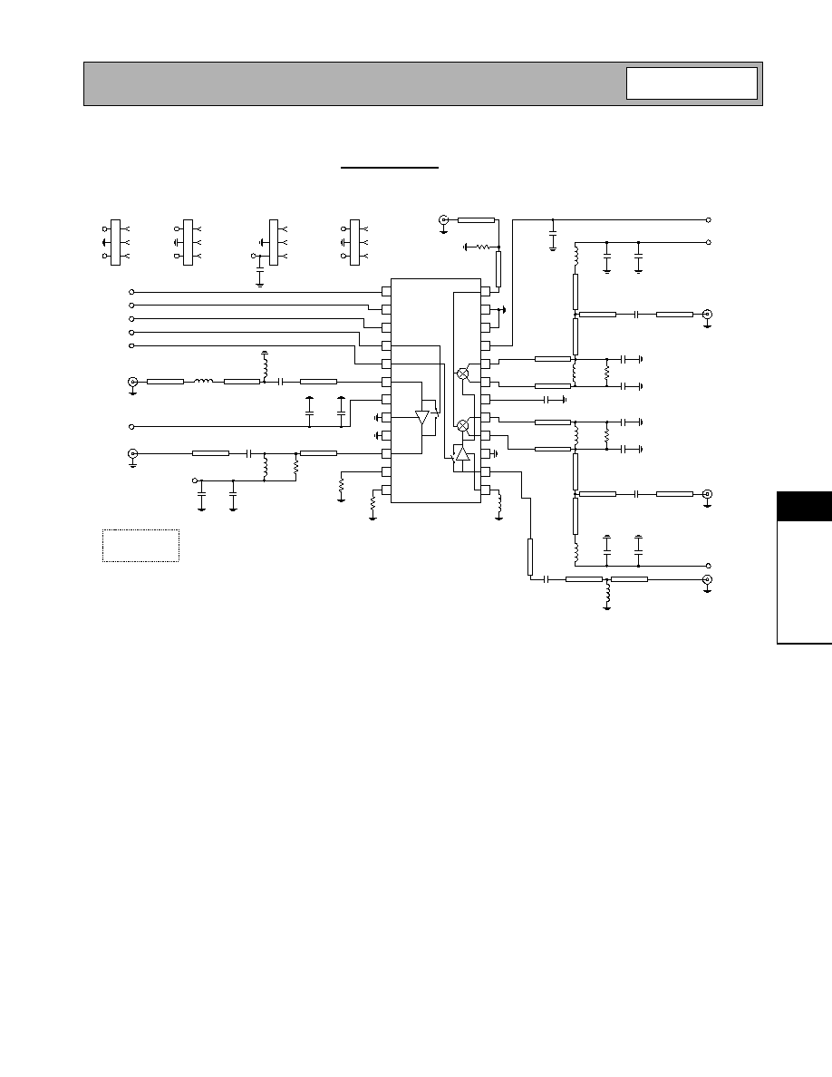
Functional Block Diagram
RF Micro Devices, Inc.
7625 Thorndike Road
Greensboro, NC 27409, USA
Tel (336) 664 1233
Fax (336) 664 0454
http://www.rfmd.com
Optimum Technology Matchingģ Applied
Si BJT
GaAs MESFET
GaAs HBT
Si Bi-CMOS
!
SiGe HBT
Si CMOS
1
2
3
4
5
6
7
8
9
10
11
12
24
23
22
21
20
19
18
17
16
15
14
13
ENABLE
IP SET
IF SEL
LNA GAIN
MIX GAIN
LNA IN
VCC1
GND1B
GND1A
LNA OUT
LO IN
GND2
GND2
VCC2
IF2+
IF2-
BYPASS
IF1-
IF1+
GND3A
MIX IN
GND3B
RF2449
CDMA/FM LOW NOISE AMPLIFIER/MIXER
900MHZ DOWNCONVERTER
∑ CDMA/FM Cellular Systems
∑ Supports Dual-Mode CDMA/AMPS
∑ Supports Dual-Mode CDMA/TACS
∑ General Purpose Downconverter
∑ Commercial and Consumer Systems
∑ Portable Battery-Powered Equipment
The RF2449 is a receiver front-end designed for the
receive section of dual-mode CDMA/FM cellular applica-
tions. It is designed to amplify and downconvert RF sig-
nals, while providing 30 dB of stepped gain control range.
Features include digital control of LNA gain, mixer gain,
LNA IIP3, and power down mode. Another feature of the
chip is adjustable IIP3 of the LNA and mixer using an off-
chip current setting resistor. The LNA IIP3 can be digitally
controlled between two levels to reduce current draw in
CDMA standby and other conditions where high IIP3 is
not required. Noise Figure, IP3, and other specs are
designed to be compatible with the IS-98 specification for
CDMA cellular communications. The IC is manufactured
on an advanced Silicon Bipolar process and packaged in
an SSOP-24.
∑ Complete Receiver Front-End
∑ Stepped LNA/Mixer Gain Control
∑ Adjustable LNA/Mixer Bias Current
∑ Adjustable LNA/Mixer IIP3
∑ Digital LNA IIP3 Control
∑ Meets IS-98 IMD and Single Tone
RF2449
CDMA/FM Low Noise Amplifier/Mixer 900MHz
Downconverter
RF2449 PCBA
Fully Assembled Evaluation Board
8
Rev A4 001016
8įMAX
0įMIN
1
0.050
0.016
0.0098
0.0075
0.2440
0.2284
0.025
0.012
0.008
0.0688
0.0532
0.157
0.150
0.0098
0.0040
0.344
0.337
Package Style: SSOP-24

Preliminary
8-76
RF2449
Rev A4 001016
8
F
R
ONT
-
E
NDS
Absolute Maximum Ratings
Parameter
Rating
Unit
Supply Voltage
-0.5 to +5.0
V
DC
Input LO and RF Levels
+6
dBm
Operating Ambient Temperature
-40 to +85
įC
Storage Temperature
-40 to +150
įC
Parameter
Specification
Unit
Condition
Min.
Typ.
Max.
Overall
T = 25įC, V
CC
= 2.75V, RF = 880MHz,
LO= 990MHz@0dBm, IF = 110MHz,
V
IPSET
< 1.0V
RF Frequency Range
869 to 894
MHz
LO Frequency Range
760 to 1010
MHz
IF Frequency Range
0.1 to 250
MHz
LNA - High Gain Mode
Gain
14
15
dB
Noise Figure
2.3
2.5
dB
IIP3
+6
dBm
IIP3 is adjustable.
LNA Out to Mixer in Isolation
40
dB
Current
3.5
mA
LNA Bypass
Gain
-6.3
dB
Noise Figure
6.3
dB
IIP3
20
dBm
Current
0
mA
Mixer - High Gain Mode
3k
balanced load.
Gain
12
13
dB
Noise Figure
6.5
7.5
dB
IIP3
+2
+3
dBm
IIP3 is adjustable - See Data Plots.
RF to IF Isolation
29
dB
Current
21
mA
Mixer - Low Gain Mode
3k
balanced load.
Gain
3
4
dB
Noise Figure
13
14
dB
IIP3
+12
+13
dBm
IIP3 is adjustable - See Data Plots.
RF to IF Isolation
35.5
dB
Current
16
mA
Local Oscillator Input
Input Level
-10
-3
0
dBm
LO to IF Isolation
40
dB
LO to RF Isolation
40
dB
LO to LNA Input Isolation
35
dB
Any gain state.
Cascade (Mode 1)
(LNA Gain High, Mix Gain High)
With -3dB image rejection filter.
Gain
24
25
27
dB
3k
balanced IF load.
Noise Figure
2.9
dB
Single sideband.
IIP3
-10
-9
dBm
Cascade (Mode 2)
(LNA Gain High, Mix Gain Low)
With -3dB image rejection filter.
Gain
16.0
dB
3k
balanced IF load.
Noise Figure
4.7
dB
Single sideband.
IIP3
0
dBm
Caution! ESD sensitive device.
RF Micro Devices believes the furnished information is correct and accurate
at the time of this printing. However, RF Micro Devices reserves the right to
make changes to its products without notice. RF Micro Devices does not
assume responsibility for the use of the described product(s).

Preliminary
8-77
RF2449
Rev A4 001016
8
F
R
ONT
-
E
NDS
Parameter
Specification
Unit
Condition
Min.
Typ.
Max.
Cascade (Mode 3)
(LNA Gain Low, Mix Gain High)
With -3dB image rejection filter.
Gain
3.5
dB
3k
balanced IF load.
Noise Figure
16
dB
Single sideband.
IIP3
+11.8
dBm
Cascade (Mode 4)
(LNA Gain Low, Mix Gain Low)
With -3dB image rejection filter.
Gain
-5
dB
3k
balanced IF load.
Noise Figure
22.5
dB
Single sideband.
IIP3
+16.0
+18.0
dBm
Power Supply
Voltage
2.65
2.75
3.9
V
Power Down Current
10
Ķ
A
Enable<1.0V

Preliminary
8-78
RF2449
Rev A4 001016
8
F
R
ONT
-
E
NDS
Pin
Function
Description
Interface Schematic
1
ENABLE
This pin is used to enable or disable the RF2449. A logic high (> 2.0V)
enables the circuitry. A logic low (<1.0V) disables the circuitry.
2
IP SET
Controls the setting of the LNA current. A logic low (< 1.0V) selects the
internal resistance (49.5k
), resulting in an LNA current of 3.5mA. A
logic high (>2.0V) selects the external resistance at pin 12.
3
IF SEL
Determines which IF port is active. A logic low (< 1.0V) activates IF1
and deactivates IF2. A logic high (> 2.0V) activates IF2 and deactivates
IF1.
4
LNA GAIN
Controls the bypass feature of the LNA. A logic low (< 1.0V) selects the
bypass mode. A logic high (>2.0V) turns on the LNA.
5
MIX GAIN
Controls the bypass feature of the mixer pre-amp. A logic low (< 1.0V)
selects the bypass mode. A logic high (>2.0V) turns on the pre-amp.
6
LNA IN
LNA input pin.
7
VCC1
VCC pin for all circuits except the LO.
8
GND1B
LNA ground pin.
See pin 6.
9
GND1A
Package ground pin.
10
LNA OUT
LNA output pin.
See pin 6.
11
ISET2
An external resistor connected to this pin sets the current of the pre-
amp and the mixer.
12
ISET1
An external resistor connected to this pin sets the current of the LNA
when IP SET is high (see pin 2).
13
GND3B
Ground pin for pre-amp circuit.
14
MIX IN
Mixer pre-amp input pin.
See pin 13.
15
GND3A
Ground pin for the mixer circuits.
16
IF1+
First differential output pin for the first mixer.
ENABLE
IP SET
IF SEL
LNA GAIN
MIX GAIN
MIX GAIN
LNA OUT
GND1B
MIX IN
GND3B
VCC2
IF1-
IF1+

Preliminary
8-79
RF2449
Rev A4 001016
8
F
R
ONT
-
E
NDS
Pin
Function
Description
Interface Schematic
17
IF1-
Second differential output pin for the first mixer.
See pin 16.
18
BYPASS
Bypass pin for the LO bias reference.
19
IF2+
First differential output pin for the second mixer.
20
IF2-
Second differential output pin for the second mixer.
See pin 20.
21
VCC2
VCC pin for the LO circuits.
22
GND2
Ground pin for the LO circuits.
23
GND2
Ground pin for the LO circuits.
24
LO IN
Local oscillator input pin.
IF2-
IF2+
LO IN

Preliminary
8-80
RF2449
Rev A4 001016
8
F
R
ONT
-
E
NDS
Application Schematic
1
2
3
4
5
6
7
8
9
10
11
12
24
23
22
21
20
19
18
17
16
15
14
13
33 nF
30 nH
6.8 nH
100 pF
6.8 nH
3.0 pF
22 k
33 k
1.5 nH 33 nF
22 nH
ENABLE
IP SET
IF SEL
LNA GAIN
MIX GAIN
*
100 pF
*NOTE:
Microstrip Inductor, Z
O
= 50
, L = 100 mils
Suggested component values for 85.38 MHz IF and
R
OUT
= 1 k
:
L1 = 470 nH
C1 = 10 pF
R = 7.5 k
RF IN
510
1 nF
V
CC
RF SAW Filter
56
LO IN
1 nF
R
L1
C1
L2
V
CC
C1
C2
L
Filter
IF2+
IF2-
100 pF
R
L1
C1
L2
1 nF
VCC
C1
C2
L
Filter
IF+
IF-
Output Interface Network
L1, C1 and R form a current combiner which performs
a differential to single-ended conversion at the IF fre-
quency and sets the output impedance. In most cases,
the resonance frequency is independent of R and can
be set according to the following equation:
Where C
EQ
is the equivalent stray capacitance and
capacitance looking into pins 16 and 17. An average
value to use for C
EQ
is 2.5pF.
R may then be used to set the output impedance
according to the following equation:
where R
OUT
is the desired output impedance and R
P
is
the parasitic equivalent parallel resistance of L1.
C1 should be chosen as high as possible, while main-
taining an R
P
of L1 that allows for the desired R
OUT
.
L2 and C2 serve dual purposes. L2 serves as an out-
put bias choke, and C2 serves as a series DC block.
In addition, L2 and C2 may be chosen to form an
impedance matching network if the input impedance of
the IF filter is not equal to ROUT. Otherwise, L2 is cho-
sen to be large and C2 is chosen to be large if a DC
path to ground is present in the IF filter, or omitted if the
filter is DC blocked.
f
IF
1
2
L1
2
------ C1
C
EQ
+
(
)
-----------------------------------------------
=
R
1
4 R
OUT
---------------------
1
R
P
------
1
≠
≠
=
Preliminary
8-81
RF2449
Rev A4 001016
8
F
R
ONT
-
E
NDS
Evaluation Board Schematic
(Download Bill of Materials from www.rfmd.com.)
1
2
3
4
5
6
7
8
9
10
11
12
24
23
22
21
20
19
18
17
16
15
14
13
50
Ķ
strip
C1
33 nF
L2
30 nH
50
Ķ
strip
L1
6.8 nH
50
Ķ
strip
C3
100 pF
C2
1 nF
VCC1
50
Ķ
strip
R1
510
L3
6.8 nH
VCC2
C6
3.0 pF
50
Ķ
strip
J2
LNA OUT
410 ps Electrical Delay @ 880 MHz
0.13 dB Line Loss
J1
LNA IN
440 ps Electrical Delay @ 880 MHz
0.14 dB Line Loss
R2
22 k
R3
33 k
L7
470 nH
R4
5.6 k
C7
5 pF
C8
5 pF
50
Ķ
strip
50
Ķ
strip
50
Ķ
strip
C9
8 pF
50
Ķ
strip
J4
IF1 OUT
268 ps Electrical Delay @ 110 MHz
0.025 dB Line Loss
L6
220 nH
C10
100 pF
C11
1 nF
VCC1
50
Ķ
strip
L4
1.5 nH
C17
33 nF
50
Ķ
strip
L5
22 nH
50
Ķ
strip
*
C18
100 pF
VCC2
C19
100 pF
50
Ķ
strip
50
Ķ
strip
J6
LO IN
313 ps Electrical Delay @ 880 MHz
0.09 dB Line Loss
J5
IF2 OUT
268 ps Electrical Delay @ 110 MHz
0.025 dB Line Loss
50
Ķ
strip
L9
470 nH
R5
5.6 k
50
Ķ
strip
50
Ķ
strip
C16
5 pF
C15
5 pF
L8
220 nH
50
Ķ
strip
C14
8 pF
50
Ķ
strip
50
Ķ
strip
C12
100 pF
C13
1 nF
VCC1
1
2
3
P2
CON3
P2-3
IF SEL
GND
P2-1
LNA GAIN
P1-1
IP SET
GND
P1-3
ENABLE
1
2
3
P1
CON3
1
2
3
P3
CON3
P3-3
C20
22 pF
MIX GAIN
GND
NC
1
2
3
P4
CON3
P4-3
VCC2
GND
P4-1
VCC1
NOTE: LE
Microstrip Inductor, Z
O
= 50
, L = 100 mils
For IF Freq. = 85 MHz
C14, C15, C5, C6 = 8 pF
L6 and L8 = 470 nH
C7 and C13 = 15 pF
50
Ķ
strip
J3
MIXER IN
290 ps Electrical Delay @ 880 MHz
0.07 dB Line Loss
50
Ķ
strip
2449400A
C5
100 pF
C4
1 nF
ENABLE
IP SET
IF SEL
LNA GAIN
MIX GAIN
R6
56

Preliminary
8-82
RF2449
Rev A4 001016
8
F
R
ONT
-
E
NDS
Evaluation Board Layout
Board Size 2.0" x 2.0"
Board Thickness 0.040", Board Material FR-4, Multi-Layer
Assembly
Top
Inner 1
Inner 2

Preliminary
8-83
RF2449
Rev A4 001016
8
F
R
ONT
-
E
NDS
Back

Preliminary
8-84
RF2449
Rev A4 001016
8
F
R
ONT
-
E
NDS
LNA - IIP3
(Low Gain Mode)
0.0
5.0
10.0
15.0
20.0
25.0
2.7
2.8
2.9
3
3.1
3.2
3.3
V
CC
(V)
IIP3 (dBm)
IIP3, -30ļ
IIP3, 25ļ
IIP3, 85ļ
LNA - IIP3
(High Gain/Low IP Mode)
0.0
1.0
2.0
3.0
4.0
5.0
6.0
7.0
8.0
9.0
2.7
2.8
2.9
3
3.1
3.2
3.3
V
CC
(V)
IIP3 (dBm)
IIP3, -30ļ
IIP3, 25ļ
IIP3, 85ļ
LNA - IIP3
(High Gain/High IP Mode)
0.0
1.0
2.0
3.0
4.0
5.0
6.0
7.0
8.0
2.7
2.8
2.9
3.0
3.1
3.2
3.3
V
CC
(V)
IIP3 (dBm)
IIP3, -30ļ
IIP3, 25ļ
IIP3, 85ļ
LNA - S21
(Low Gain Mode)
-6.8
-6.7
-6.6
-6.5
-6.4
-6.3
-6.2
-6.1
-6.0
2.7
2.8
2.9
3.0
3.1
3.2
3.3
V
CC
(V)
S21 (dB)
S21, -30ļ
S21, 25ļ
S21, 85ļ
LNA - S21
(High Gain/Low IP Mode)
14.1
14.2
14.3
14.4
14.5
14.6
14.7
14.8
14.9
15.0
2.7
2.8
2.9
3.0
3.1
3.2
3.3
V
CC
(V)
S21 (dB)
S21, -30ļ
S21, 25ļ
S21, 85ļ
LNA - S21
(High Gain/High IP Mode)
14.4
14.5
14.6
14.7
14.8
14.9
15.0
15.1
15.2
15.3
15.4
2.7
2.8
2.9
3.0
3.1
3.2
3.3
V
CC
(V)
S21 (dB)
S21, -30ļ
S21, 25ļ
S21, 85ļ

Preliminary
8-85
RF2449
Rev A4 001016
8
F
R
ONT
-
E
NDS
LNA - Noise Figure
(Low Gain Mode)
0.0
1.0
2.0
3.0
4.0
5.0
6.0
7.0
8.0
2.7
2.8
2.9
3.0
3.1
3.2
3.3
V
CC
(V)
NF (dB)
NF, -30ļ
NF, 25ļ
NF, 85ļ
LNA - Noise Figure
(High Gain/Low IP Mode)
0.0
0.5
1.0
1.5
2.0
2.5
3.0
2.7
2.8
2.9
3.0
3.1
3.2
3.3
V
CC
(V)
NF (dB)
NF, -30ļ
NF, 25ļ
NF, 85ļ
LNA - Noise Figure
(High Gain/High IP Mode)
0.0
0.5
1.0
1.5
2.0
2.5
3.0
2.7
2.8
2.9
3.0
3.1
3.2
3.3
V
CC
(V)
NF (dB)
NF, -30ļ
NF, 25ļ
NF, 85ļ

Preliminary
8-86
RF2449
Rev A4 001016
8
F
R
ONT
-
E
NDS
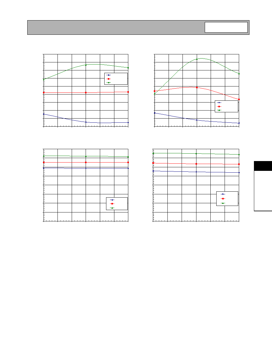
Mixer - RF to IF1 Isolation
(High Gain Mode)
28.0
28.2
28.4
28.6
28.8
29.0
29.2
29.4
29.6
29.8
30.0
2.7
2.8
2.9
3.0
3.1
3.2
3.3
V
CC
(V)
RF to IF1 Isolation (dB)
Isolation, -30ļ
Isolation, 25ļ
Isolation, 85ļ
Mixer - LO to IF1 Isolation
(Low Gain Mode)
41.2
41.4
41.6
41.8
42.0
42.2
42.4
42.6
42.8
43.0
2.7
2.8
2.9
3.0
3.1
3.2
3.3
V
CC
(V)
LO to IF1 Isolation (dB)
Isolation, -30ļ
Isolation, 25ļ
Isolation, 85ļ
Mixer - IIP3
(Low Gain Mode)
0.0
2.0
4.0
6.0
8.0
10.0
12.0
14.0
16.0
2.7
2.8
2.9
3.0
3.1
3.2
3.3
V
CC
(V)
IIP3 (dBm)
IIP3, -30ļ
IIP3, 25ļ
IIP3, 85ļ
Mixer - IIP3
(High Gain Mode)
0.0
1.0
2.0
3.0
4.0
5.0
6.0
2.7
2.8
2.9
3.0
3.1
3.2
3.3
V
CC
(V)
IIP3 (dB)
IIP3, -30ļ
IIP3, 25ļ
IIP3, 85ļ
Mixer - RF to IF1 Isolation
(Low Gain Mode)
34.6
34.8
35.0
35.2
35.4
35.6
35.8
36.0
36.2
36.4
36.6
36.8
2.7
2.8
2.9
3.0
3.1
3.2
3.3
V
CC
(V)
RF to IF1 Isolation (dB)
Isolation, -30ļ
Isolation, 25ļ
Isolation, 85ļ
Mixer - LO to IF1 Isolation
(High Gain Mode)
42.6
42.8
43.0
43.2
43.4
43.6
43.8
44.0
44.2
2.7
2.8
2.9
3.0
3.1
3.2
3.3
V
CC
(V)
LO to IF1 Isolation (dB)
Isolation, -30ļ
Isolation, 25ļ
Isolation, 85ļ
Preliminary
8-87
RF2449
Rev A4 001016
8
F
R
ONT
-
E
NDS
Mixer - Noise Figure
(High Gain Mode)
0.0
1.0
2.0
3.0
4.0
5.0
6.0
7.0
8.0
2.7
2.8
2.9
3.0
3.1
3.2
3.3
V
CC
(V)
NF (dB)
NF, -30ļ
NF, 25ļ
NF, 85ļ
Mixer - LO to RF Isolation
(High Gain Mode)
45.0
45.5
46.0
46.5
47.0
47.5
48.0
48.5
49.0
49.5
2.7
2.8
2.9
3.0
3.1
3.2
3.3
V
CC
(V)
LO to RF Isolation (dB)
Isolation, -30ļ
Isolation, 25ļ
Isolation, 85ļ
Mixer - Noise Figure
(Low Gain Mode)
0.0
2.0
4.0
6.0
8.0
10.0
12.0
14.0
16.0
2.7
2.8
2.9
3.0
3.1
3.2
3.3
V
CC
(V)
NF (dB)
NF, -30ļ
NF, 25ļ
NF, 85ļ
Mixer - LO to RF Isolation
(Low Gain Mode)
42.0
42.5
43.0
43.5
44.0
44.5
45.0
45.5
46.0
46.5
2.7
2.8
2.9
3.0
3.1
3.2
3.3
V
CC
(V)
LO to RF Isolation (dB)
Isolation, -30ļ
Isolation, 25ļ
Isolation, 85ļ

Preliminary
8-88
RF2449
Rev A4 001016
8
F
R
ONT
-
E
NDS