
¸
8-97
8
F
R
O
N
T
-
E
NDS
Product Description
Ordering Information
Typical Applications
Features
Functional Block Diagram
RF Micro Devices, Inc.
7628 Thorndike Road
Greensboro, NC 27409, USA
Tel (336) 664 1233
Fax (336) 664 0454
http://www.rfmd.com
Optimum Technology MatchingÆ Applied
Si BJT
GaAs MESFET
GaAs HBT
Si Bi-CMOS
SiGe HBT
Si CMOS
1
LO IN
2
GND2
3
VCC
4
GND1
8
IF+
7
IF-
6
GND3
5
RF IN
RF2459
3V PCS DOWNCONVERTER
∑ CDMA/TDMA/DCS1900 PCS Systems
∑ PHS 1500/WLAN 2400 Systems
∑ General Purpose Downconverter
∑ Micro-Cell PCS Base Stations
∑ Portable Battery-Powered Equipment
The RF2459 is a monolithic integrated downconverter for
PCS, PHS, and WLAN applications. The IC contains all of
the required components to implement the RF functions
of the downconverter. It contains a double-balanced Gil-
bert cell mixer and a balanced IF output. The mixer's high
third-order intercept point makes it ideal for digital cellular
applications. The IC is designed to operate from a single
3 V power supply.
∑ Extremely High Dynamic Range
∑ Single 3V Power Supply
∑ 1500MHz to 2500MHz Operation
RF2459
3V PCS Downconverter
RF2459 PCBA
Fully Assembled Evaluation Board
8
Rev A3 011105
NOTES:
1. Shaded lead is pin 1.
2. All dimensions are exclusive of
flash, protrusions or burrs.
3. Lead coplanarity: 0.002 with
respect to datum "A".
0.012
6∞ MAX
0∞ MIN
0.021
+ 0.004
0.006
+ 0.002
0.192
+ 0.008
0.0256
0.118
+ 0.004 sq.
0.006
+ 0.003
0.034
-A-
Package Style: MSOP-8

8-98
RF2459
Rev A3 011105
8
F
R
O
N
T
-
E
NDS
Absolute Maximum Ratings
Parameter
Ratings
Unit
Supply Voltage
-0.5 to 7.0
V
DC
Input LO and RF Levels
+6
dBm
Ambient Operating Temperature
-40 to +85
∞C
Storage Temperature
-40 to +150
∞C
Parameter
Specification
Unit
Condition
Min.
Typ.
Max.
Overall
T = 25∞C, V
CC
= 3.0V, RF = 1960MHz,
LO= 1750MHz@-2dBm
Usable RF Frequency Range
1500
2500
MHz
Typical RF Frequency Range
1930 to 1990
MHz
Usable LO Frequency Range
1200
2500
MHz
Typical LO Frequency Range
1430 to 1990
MHz
IF Frequency Range
DC to 500
MHz
Noise Figure
14
dB
Input VSWR
<2:1
Single-ended with external matching net-
work.
Input IP3
+5.0
+7.0
dBm
Gain
8
10
dB
Output Impedance
1000
Single-ended with external matching net-
work.
Input P1dB
-7.5
dBm
LO Input
LO Input Range
-5 to +3
dBm
LO to RF (Mix In) Rejection
30
dB
LO to IF
40
dB
LO Input VSWR
<2:1
Single-ended with external matching net-
work.
Power Supply
Voltage
2.7
3.0
3.6
V
Current Consumption
20
26
mA
Caution! ESD sensitive device.
RF Micro Devices believes the furnished information is correct and accurate
at the time of this printing. However, RF Micro Devices reserves the right to
make changes to its products without notice. RF Micro Devices does not
assume responsibility for the use of the described product(s).

8-99
RF2459
Rev A3 011105
8
F
R
O
N
T
-
E
NDS
Pin
Function
Description
Interface Schematic
1
LO IN
Mixer LO single-ended input. The pin is internally DC blocked. External
matching sets impedance.
2
GND2
Ground for downconverter. Keep traces physically short and connect
directly to ground plane for best performance.
3
VCC
Supply voltage for downconverter. External RF bypassing is required.
The trace length between the bypass caps and the pin should be mini-
mized. Connect ground sides of caps directly to ground.
4
GND1
Same as pin 2.
5
RF IN
Mixer RF single-ended input. The pin is internally DC blocked. External
matching sets input impedance.
6
GND3
Same as pin 2.
7
IF-
IF output pin. The output is balanced. A current combiner external net-
work performs a differential to single-ended conversion and sets the
output impedance. There must be a DC path from V
CC
to this pin. this
is normally achieved with the current combiner network. A DC blocking
cap must be present if the IF filter input has a DC path to ground.
8
IF+
Same as pin 7, except complementary output.
LO IN
RF IN
IF+ IF-

8-100
RF2459
Rev A3 011105
8
F
R
O
N
T
-
E
NDS
Application Schematic
1
2
3
4
8
7
6
5
4.7 nH
1.5 pF
22 pF
100 nF
1.5 pF
2.2 nH
R
L1
C1
C1
C2
L2
V
CC
V
CC
LO IN
RF IN
IF OUT
IF Filter
Output Interface Network
L1, C1 and R form a current combiner which performs
a differential to single-ended conversion at the IF fre-
quency and sets the output impedance. In most cases,
the resonance frequency is independent of R and can
be set according to the following equation:
Where C
EQ
is the equivalent stray capacitance and
capacitance looking into pins 7 and 8. An average
value to use for C
EQ
is 2.5pF.
R can then be used to set the output impedance
according to the following equation:
where R
OUT
is the desired output impedance and R
P
is
the parasitic equivalent parallel resistance of L1.
C1 should be chosen as high as possible, while main-
taining an R
P
of L1 that allows for the desired R
OUT
.
L2 and C2 serve dual purposes. L2 serves as an out-
put bias choke, and C2 serves as a series DC block.
In addition, L2 and C2 may be chosen to form an
impedance matching network if the input impedance of
the IF filter is not equal to ROUT. Otherwise, L2 is cho-
sen to be large (suggested 8.2nH) and C2 is chosen to
be large (suggested 22nF) if a DC path to ground is
present in the IF filter, or omitted if the filter is DC
blocked.
1
2
L1
2
(C1 + C
EQ
)
f
IF
=
R =
1
4 R
OUT
-
1
R
P
(
)
-1

8-101
RF2459
Rev A3 011105
8
F
R
O
N
T
-
E
NDS
Evaluation Board Schematic
RF=1.959MHz, IF=210MHz
(Download Bill of Materials from www.rfmd.com.)
1
2
3
4
8
7
6
5
L1
4.7 nH
C1
1.5 pF
J1
LO IN
C3
22 pF
C2
100 nF
VCC
C4
1.5 pF
L2
2.2 nH
J2
RF IN
R1
16k
L3
100 nH
C5
9 pF
C6
9 pF
C7
4 pF
J3
IF OUT
L4
180 nH
VCC
50
µ
strip
50
µ
strip
50
µ
strip
VCC
GND
N/C
1
2
3
P1
CON3
NOTES:
1) R1, L3, C5, and C6 are chosen to produce an output impedance, R
OUT
, of 1000
@ 210 MHz.
2) L4 and C7 are chosen to match the 1000
output impedance to 50
for testing purposes.

8-102
RF2459
Rev A3 011105
8
F
R
O
N
T
-
E
NDS
Evaluation Board Layout 900MHz
Board Size 2.0" x 2.0"
Board Thickness 0.031", Board Material FR-4
8-103
RF2459
Rev A3 011105
8
F
R
O
N
T
-
E
NDS
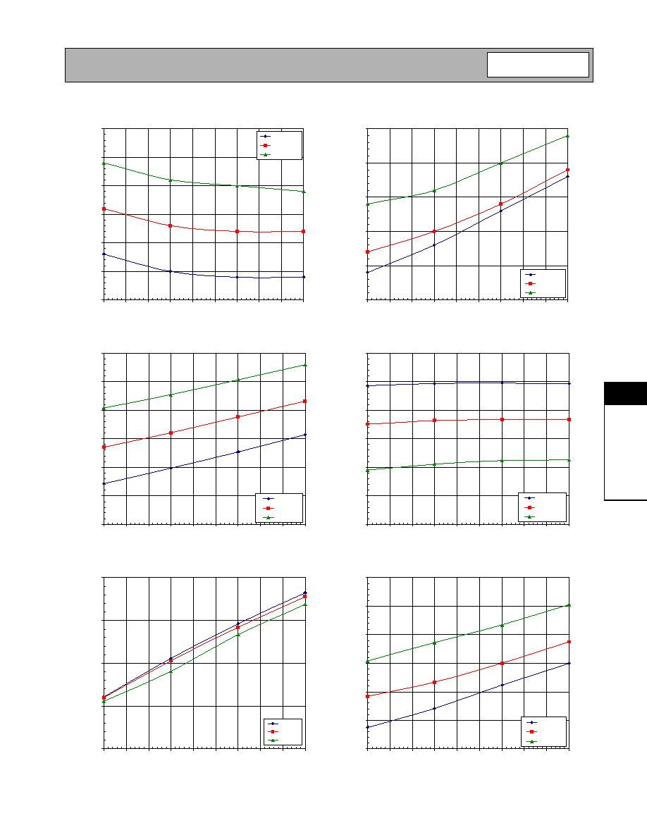
MIX
IN
VSWR versus V
CC
1.65
1.70
1.75
1.80
1.85
1.90
1.95
2.70
2.80
2.90
3.00
3.10
3.20
3.30
3.40
3.50
3.60
V
CC
(V)
MIX
IN
VSWR
MIXin, -30∫
MIXin, 25∫
MIXin, 85∫
LO
IN
VSWR versus V
CC
1.20
1.25
1.30
1.35
1.40
1.45
2.70
2.80
2.90
3.00
3.10
3.20
3.30
3.40
3.50
3.60
V
CC
(V)
LO
IN
Loin, -30∫
Loin, 25∫
Loin, 85∫
NF versus V
CC
11.0
12.0
13.0
14.0
15.0
16.0
17.0
2.7
2.8
2.9
3.0
3.1
3.2
3.3
3.4
3.5
3.6
V
CC
(V)
Noise
Figure
NF, -30∫
NF, 25∫
NF, 85∫
Gain versus V
CC
7.0
8.0
9.0
10.0
11.0
12.0
13.0
2.7
2.8
2.9
3.0
3.1
3.2
3.3
3.4
3.5
3.6
V
CC
(V)
Gain
(dB)
Gain, -30∫
Gain, 25∫
Gain, 85∫
I
CC
versus V
CC
10.0
15.0
20.0
25.0
30.0
2.7
2.8
2.9
3.0
3.1
3.2
3.3
3.4
3.5
3.6
V
CC
(V)
I
CC
(mA)
Icc, -30∫
Icc, 25∫
Icc, 85∫
IIP3 versus V
CC
3.0
5.0
7.0
9.0
11.0
13.0
15.0
2.7
2.8
2.9
3.0
3.1
3.2
3.3
3.4
3.5
3.6
V
CC
(V)
IIP3
(dBm)
IIP3, -30∫
IIP3, 25∫
IIP3, 85∫

8-104
RF2459
Rev A3 011105
8
F
R
O
N
T
-
E
NDS
IP1dB versus V
CC
-10.0
-9.0
-8.0
-7.0
-6.0
-5.0
-4.0
2.7
2.8
2.9
3.0
3.1
3.2
3.3
3.4
3.5
3.6
V
CC
(V)
IP1dB
(dBm)
IP1dB, -30∫
IP1dB, 25∫
IP1dB, 85∫
Gain versus LO P
IN
V
CC
= 3.0 V
7.0
8.0
9.0
10.0
11.0
12.0
13.0
14.0
-6.0
-4.0
-2.0
0.0
2.0
4.0
LO P
IN
(dBm)
Gain
(dB)
Gain, -30∫
Gain, 25∫
Gain, 85∫
IIP3 versus LO P
IN
V
CC
= 3.0 V
0.0
2.0
4.0
6.0
8.0
10.0
12.0
14.0
-6.0
-4.0
-2.0
0.0
2.0
4.0
LO P
IN
(dBm)
IIP3
(dBm)
IIP3, -30∫
IIP3, 25∫
IIP3, 85∫
IP1dB versus LO P
IN
V
CC
= 3.0 V
-12.0
-11.0
-10.0
-9.0
-8.0
-7.0
-6.0
-5.0
-6.0
-4.0
-2.0
0.0
2.0
4.0
LO P
IN
(dBm)
IP1dB
(dBm)
IP1dB, -30∫
IP1dB, 25∫
IP1dB, 85∫