 | –≠–ª–µ–∫—Ç—Ä–æ–Ω–Ω—ã–π –∫–æ–º–ø–æ–Ω–µ–Ω—Ç: RF2461 | –°–∫–∞—á–∞—Ç—å:  PDF PDF  ZIP ZIP |
¸
8-123
8
F
R
O
N
T
-
E
NDS
Preliminary
Product Description
Ordering Information
Typical Applications
Features
Functional Block Diagram
RF Micro Devices, Inc.
7625 Thorndike Road
Greensboro, NC 27409, USA
Tel (336) 664 1233
Fax (336) 664 0454
http://www.rfmd.com
Optimum Technology MatchingÆ Applied
Si BJT
GaAs MESFET
GaAs HBT
Si Bi-CMOS
SiGe HBT
Si CMOS
IF2+
15
IF2-
14
BYPASS
13
IF1+
12
IF1-
11
MIX
I
N
10
G
ND3B
9
I
SET
1
8
I
SET
2
7
LNA
O
UT
6
GND1B
5
VCC1
4
LNA IN
3
MIX GAIN
2
LNA GAIN
1
I
F
SEL
20
I
P
SET
19
EN
ABL
E
18
LO
IN
17
V
CC2
16
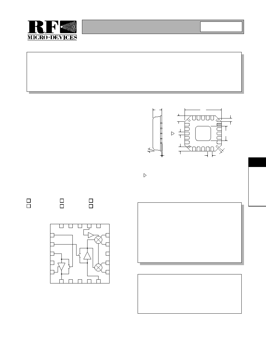
RF2461
CDMA/FM LOW NOISE AMPLIFIER/MIXER
900MHZ DOWNCONVERTER
∑ CDMA/FM Cellular Systems
∑ Supports Dual-Mode AMPS/CDMA
∑ Supports Dual-Mode TACS/JCDMA
∑ General Purpose Downconverter
∑ Commercial and Consumer Systems
∑ Portable Battery-Powered Equipment
The RF2461 is a receiver front-end designed for the
receive section of dual-mode CDMA/FM cellular applica-
tions. It is designed to amplify and downconvert RF sig-
nals, while providing 30dB of stepped gain control range.
Features include digital control of LNA gain, mixer gain,
and power down mode. Another feature of the chip is
adjustable IIP3 of the LNA and mixer using an off-chip
current setting resistor. Noise figure, IP3, and other specs
are designed to be compatible with the IS-98B interim
standard for CDMA cellular communications. The IC is
manufactured on an advanced Silicon Germanium HBT
process and is in a 4 mmx4mm, 20-pin, leadless chip car-
rier.
∑ Complete Receiver Front-End
∑ Stepped LNA/Mixer Gain Control
∑ Adjustable LNA/Mixer Bias Current
∑ Adjustable LNA/Mixer IIP3
∑ Meets IMD Tests with Three Gain States/
Two Logic Control Lines
RF2461
CDMA/FM Low Noise Amplifier/Mixer 900MHz
Downconverter
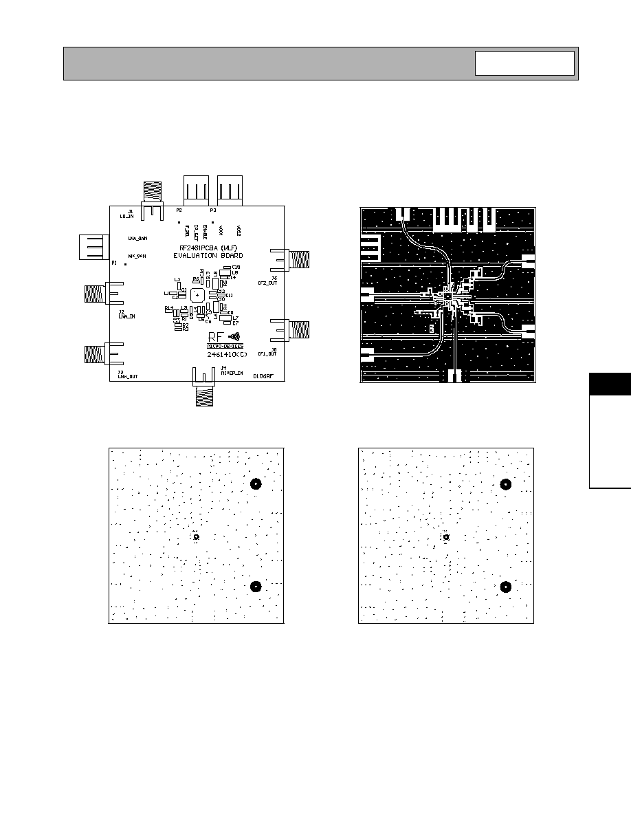
RF2461 PCBA
Fully Assembled Evaluation Board
8
Rev A13 010607
1.00
0.90
4.00
sq.
0.60
0.24 typ
3
0.20
0.75
0.50
0.23
0.13
4 PLCS
0.50
2.10
sq.
0.65
0.30
4 PLCS
0.05
12∞
MAX
Dimensions in mm.
Note orientation of package.
NOTES:
Package Warpage: 0.05 mm max.
4
Die Thickness Allowable: 0.305 mm max.
5
Pin 1 identifier must exist on top surface of package by identification
mark or feature on the package body. Exact shape and size is optional.
2
Shaded lead is Pin 1.
1
Dimension applies to plated terminal: to be measured between 0.02 mm
and 0.25 mm from terminal end.
3
Package Style: LCC, 20-Pin, 4x4
Preliminary
8-124
RF2461
Rev A13 010607
8
F
R
O
N
T
-
E
NDS
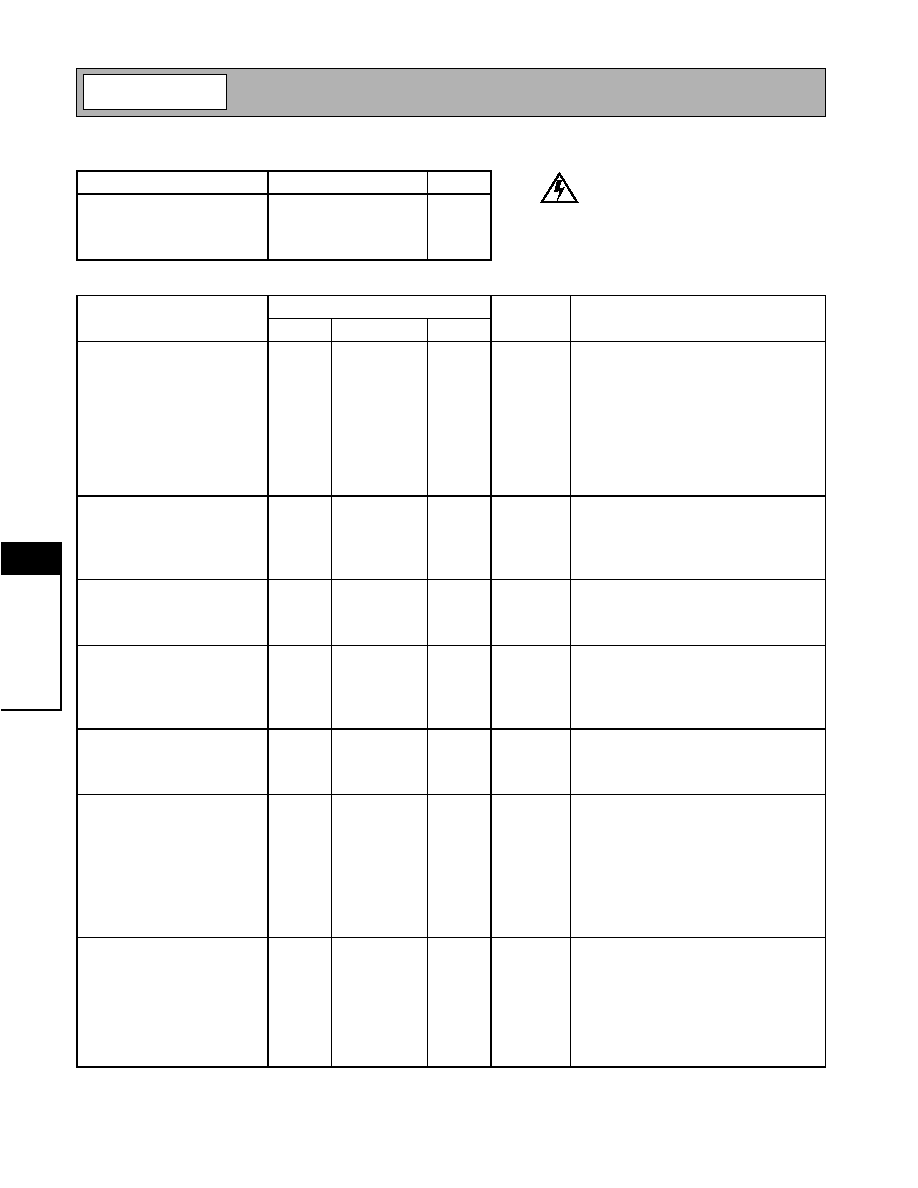
Absolute Maximum Ratings
Parameter
Rating
Unit
Supply Voltage
-0.5 to +5.0
V
DC
Input LO and RF Levels
+6
dBm
Operating Ambient Temperature
-40 to +85
∞C
Storage Temperature
-40 to +150
∞C
Parameter
Specification
Unit
Condition
Min.
Typ.
Max.
Overall
T = 25∞C, V
CC
= 3.0V
CDMA: RF = 880MHz, IF= 85MHz,
LO= 965MHz@-10dBm
JCDMA: RF= 851MHz, IF = 110MHz,
LO= 741MHz@-4dBm
RF Frequency Range
800
869 to 894
1000
MHz
832 to 870
LO Frequency Range
700
954 to 979
1000
MHz
722 to 760
IF Frequency Range
0.1
250
MHz
LNA - CDMA
Gain
13.5
14.5
15
dB
Noise Figure
1.8
2
dB
Input IP3
+7.0
+9.0
dBm
IIP3 is adjustable. V
IPSET
=0V
Current
5
mA
LNA Bypass - CDMA
Gain
-8
-6
dB
Input IP3
+16.0
+18.0
dBm
Current
0
mA
LNA - JCDMA
Gain
14
15
16
dB
Noise Figure
1.8
2
dB
Input IP3
+9.0
+11.0
dBm
IIP3 is adjustable. V
IPSET
=3V
Current
6.5
mA
LNA Bypass - JCDMA
Gain
-9
-7
dB
Input IP3
+20.0
+24.0
dBm
Current
0
mA
Mixer - High Gain Mode -
CDMA
3k
balanced load.
Gain
13
14.5
dB
Noise Figure
5.5
7
dB
Input IP3
+3.0
+4.0
dBm
IIP3 is adjustable. Decreasing R4/R5 will
increase IIP3.
RF to IF Isolation
dB
Current
(including LO Buffer/Bias)
21
mA
Mixer - Low Gain Mode -
CDMA
Gain
4
5.8
dB
Noise Figure
13
14
dB
IIP3
+13.0
+14.0
dBm
RF to IF Isolation
dB
Current
(including LO Buffer/Bias)
18
mA
Caution! ESD sensitive device.
RF Micro Devices believes the furnished information is correct and accurate
at the time of this printing. However, RF Micro Devices reserves the right to
make changes to its products without notice. RF Micro Devices does not
assume responsibility for the use of the described product(s).
Preliminary
8-125
RF2461
Rev A13 010607
8
F
R
O
N
T
-
E
NDS
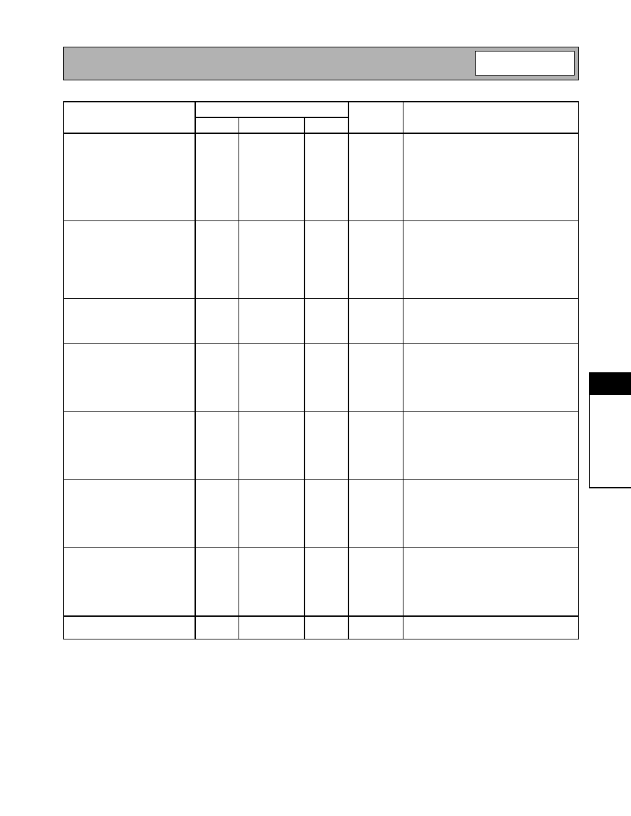
Parameter
Specification
Unit
Condition
Min.
Typ.
Max.
Mixer - High Gain Mode -
JCDMA
3k
balanced load.
Gain
12
13
dB
Noise Figure
5.5
7
dB
Input IP3
+2.0
+3.0
dBm
IIP3 is adjustable. Decreasing R4/R5 will
increase IIP3.
Current
(including LO Buffer/Bias)
24
mA
Mixer - Low Gain Mode -
JCDMA
Gain
2.5
4.0
dB
Noise Figure
13
14
dB
IIP3
+10.0
+12.0
dBm
Current
(including LO Buffer/Bias)
21
mA
Local Oscillator Input
Input Level
-10
dBm
LO to IF Isolation
-70
dB
LO to LNA Isolation
-60
dB
Any gain state.
Cascade -
LNA High/Mixer High
LNA High Gain/Mixer High Gain.
Assumes 3dB Image filter insertion loss.
Gain
23.5
26
28
dB
Noise Figure
2.4
dB
Input IP3
-11
-9
0
dBm
Current
26
mA
Cascade -
LNA High/Mixer Low
LNA High Gain/Mixer Low Gain.
Assumes 3dB Image filter insertion loss.
Gain
16.5
dB
Noise Figure
4.9
dB
Input IP3
0
dBm
Current
23
mA
Cascade -
LNA Low/Mixer High
LNA Low Gain/Mixer High Gain.
Assumes 3dB Image filter insertion loss.
Gain
4
dB
Noise Figure
15.5
dB
Input IP3
11.8
dBm
Current
22
mA
Cascade -
LNA Low/Mixer Low
LNA Low Gain/Mixer Low Gain.
Assumes 3dB Image filter insertion loss.
Gain
-7
-4.5
-3
dB
Noise Figure
22.5
dB
Input IP3
+14
+20
40
dBm
Current
18
mA
Power Supply
Voltage
2.65
3.0
3.15
V
Preliminary
8-126
RF2461
Rev A13 010607
8
F
R
O
N
T
-
E
NDS
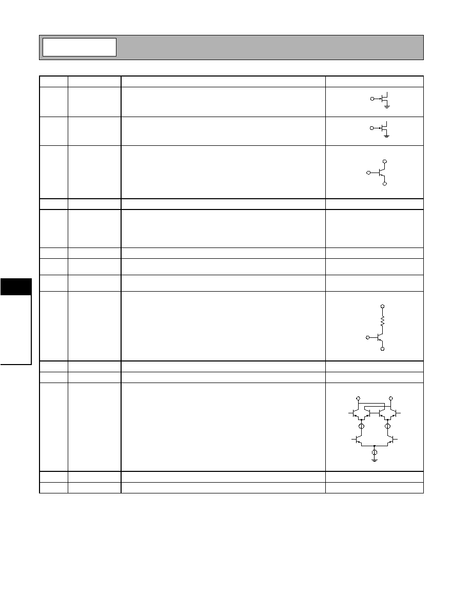
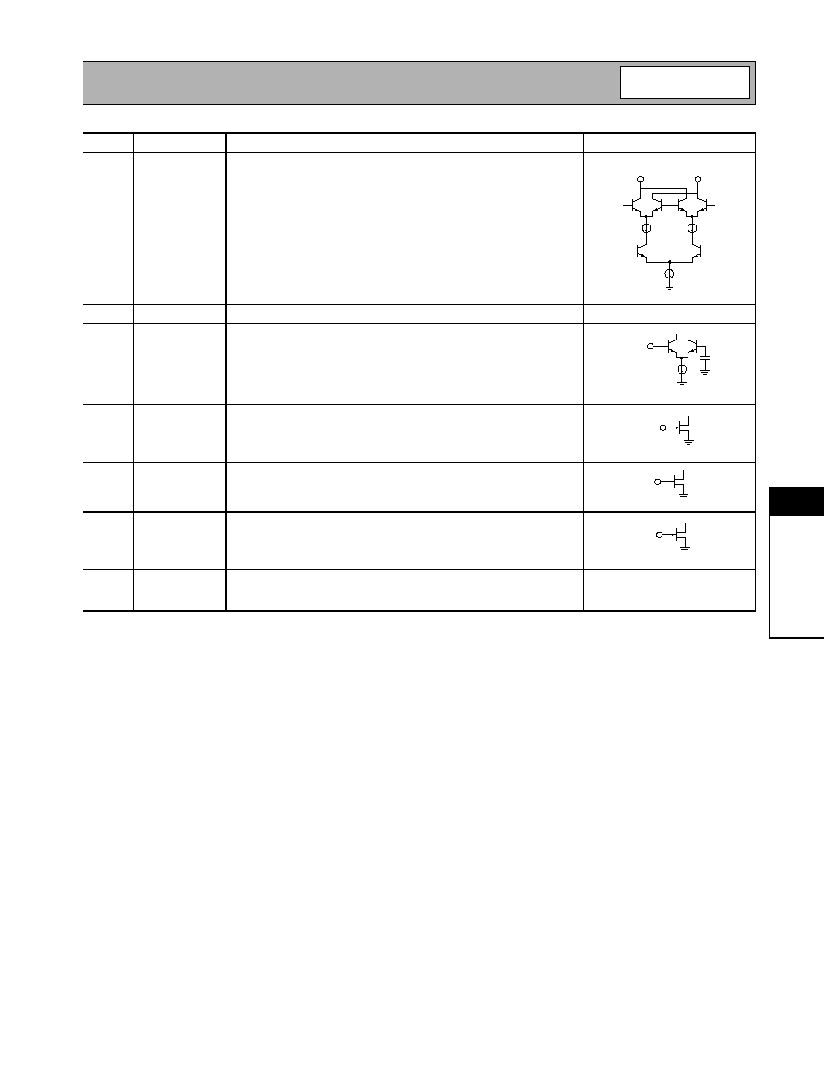
Pin
Function
Description
Interface Schematic
1
LNA GAIN
Controls the bypass feature of the LNA. A logic low (< 1.0V) selects the
bypass mode. A logic high (>2.0V) turns on the LNA.
2
MIX GAIN
Controls the bypass feature of the mixer pre-amp. A logic low (< 1.0V)
selects the bypass mode. A logic high (>2.0V) turns on the pre-amp.
3
LNA IN
LNA input pin.
4
VCC1
VCC pin for all circuits except the LO. Buffer/bias circuitry.
5
GND1B
LNA emitter. This pin provides the DC path to ground for the LNA. A
lumped element or a transmission line inductor can be placed between
this pin and ground to degenerate the LNA. This will decrease the gain,
increase the IP3, and increase the NF of the LNA. As the value of
inductance is increased, these effects will become more pronounced.
6
LNA OUT
LNA output pin.
See pin 3.
7
ISET2
An external resistor R2 connected to this pin sets the current of the pre-
amp and the mixer.
8
ISET1
An external resistor R3 connected to this pin sets the current of the
LNA when IP SET is high (see pin 19).
9
GND3B
Ground pin for pre-amp circuit. A 3.3nH inductor is used between pin 9
and ground to degenerate the mixer pre-amp. Degenerating the pre-
amp will reduce the gain, increase the IP3 and affect the pre-amp input
impedance.
10
MIX IN
Mixer pre-amp input pin.
See pin 9.
11
IF1-
Second differential output pin for the first mixer.
See pin 12.
12
IF1+
First differential output pin for the first mixer. Open collector. A current
combiner external network performs a differential to single-ended con-
version and sets the output impedance. A DC blocking cap must be
present if the IF filter input has a DC path to ground. Mixer (IF2+ and
IF-) needs to "see" a differential impedance between 2k
to 4k
.
13
BYPASS
Bypass pin for the LO bias reference.
14
IF2-
Second differential output pin for the second mixer.
See pin 15.
LNA GAIN
MIX GAIN
LNA IN
LNA OUT
GND1B
MIX IN
GND3B
VCC2
IF1-
IF1+
Preliminary
8-127
RF2461
Rev A13 010607
8
F
R
O
N
T
-
E
NDS
*The bias circuitry current drop when LO signal is not present. Total LO buffer/bias circuitry current is 7 mA when LO sig-
nal is present.
Pin
Function
Description
Interface Schematic
15
IF2+
First differential output pin for the second mixer. Open collector. A cur-
rent combiner external network performs a differential to single-ended
conversion and sets the output impedance. A DC blocking cap must be
present if the IF filter input has a DC path to ground. Mixer (IF2+ and
IF2-) needs to "see" a differential impedance between 2k
to 4k
.
16
VCC2
VCC pin for the LO buffer/bias circuitry.*
17
LO IN
LO limiter input pin.
18
ENABLE
This pin is used to enable or disable the RF2461. A logic high (> 2.0V)
enables the circuitry. A logic low (<1.0V) disables the circuitry.
19
IP SET
Controls the setting of the LNA current. A logic low (< 1.0V) selects the
internal resistance (49.5k
), resulting in an LNA current of 5mA. A
logic high (> 2.0V) selects the external resistance at pin 8.
20
IF SEL
Determines which IF port is active. A logic low (< 1.0V) activates IF1
and deactivates IF2. A logic high (> 2.0V) activates IF2 and deactivates
IF1.
Pkg
Base
GND
Ground connection. The backside of the package should be soldered to
a top side ground pad which is connected to the ground plane with mul-
tiple vias.
IF2-
IF2+
LO IN
ENABLE
IP SET
IF SEL

Preliminary
8-128
RF2461
Rev A13 010607
8
F
R
O
N
T
-
E
NDS
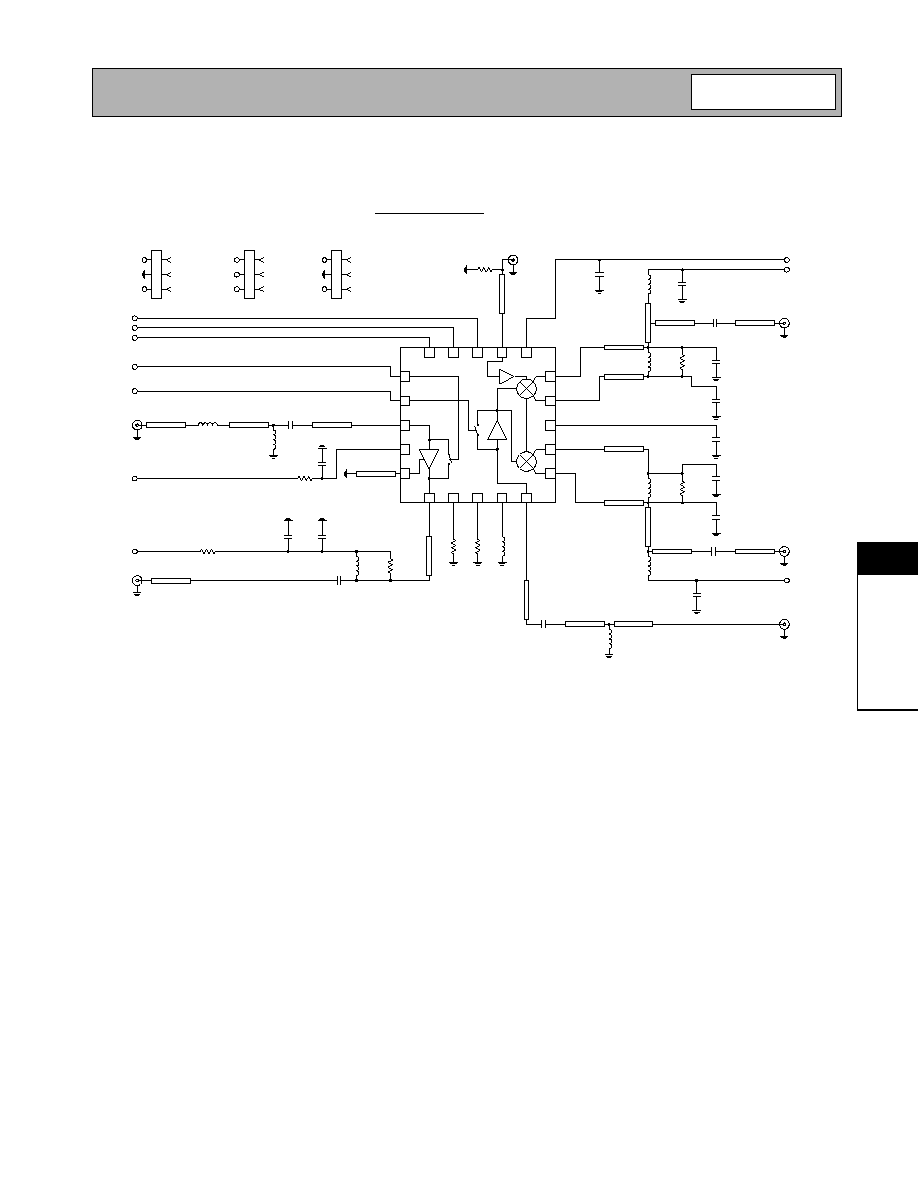
Application Schematic
15
14
13
12
11
10
9
8
7
6
5
4
3
2
1
20
19
18
17
16
VCC1
100 pF
33 nF
16 nH
4.3 nH
IF SEL
100 pF
56
L2
100 pF
C2
L1
R
C1
C1
100 pF
C2
L1
R
C1
C1
L2
VCC1
100 pF
50
µ
strip
620
4 pF
100 pF
0.1
µ
F
VCC1
22 k
47 k
3.3 nH
LNA GAIN
MIX GAIN
VCC2
VCC1
NOTE:
Microstrip Inductor, Z
0
= 50
, L = 102 mils
suggested compared values.
51
*
Filter
33 nF
47 nH
L
Filter
IF+
IF-
L
Filter
IF2+
IF2-
LO IN
LNA IN
7.5 nH
50
µ
strip
L=130 mils
W=12 mils
Z
0
=50
ENABLE
IP SET
*This resistor improves NF and IIP3 for
V
CC
= 3.0 V.
BYPASS
51
Output Interface Network
L1, C1, and R form a current combiner which performs
a differential to single-ended conversion at the IF fre-
quency and sets the output impedance. In most cases,
the resonance frequency is independent of R and can
be set according to the following equation:
Where C
EQ
is the equivalent stray capacitance and
capacitance looking into pins 11 and 12. An average
value to use for C
EQ
is 2.5pF to 3 pF.
R can then be used to set the output impedance
according to the following equation:
where R
OUT
is the desired output impedance and R
P
is
the parasitic equivalent parallel resistance of L1.
C1 should be chosen as high as possible (not greater
than 15pF), while maintaining an R
P
of L1 that allows
for the desired R
OUT
.
L2 and C2 serve dual purposes. L2 serves as an out-
put bias choke, and C2 serves as a series DC block.
In addition, L2 and C2 may be chosen to form an
impedance matching network if the input impedance of
the IF filter is not equal to ROUT. Otherwise, L2 is cho-
sen to be large, and C2 is chosen to be large if a DC
path to ground is present in the IF filter, or omitted if the
filter is DC blocked.
1
2
L1
2
(C1 + C
EQ
)
f
IF
=
R =
1
4 R
OUT
-
1
R
P
(
)
-1
Preliminary
8-129
RF2461
Rev A13 010607
8
F
R
O
N
T
-
E
NDS
Evaluation Board Schematic - CDMA
LO@965MHz, RF@880MHz, IF@85MHz
(Download Bill of Materials from www.rfmd.com.)
15
14
13
12
11
10
9
8
7
6
5
4
3
2
1
20
19
18
17
16
VCC1
50
µ
strip
C1
33 nF
L2
16 nH
50
µ
strip
L1
4.3 nH
50
µ
strip
IF SEL
ENABLE
IP SET
C16
100 pF
50
µ
strip
R6
56
50
µ
strip
50
µ
strip
L8
390 nH
C15
100 pF
50
µ
strip
C14
11 pF
50
µ
strip
L9
470 nH
50
µ
strip
R5
10 k
C13
10 pF
C12
11 pF
C11
100 pF
50
µ
strip
C8
11 pF
50
µ
strip
L6
470 nH
R4
10 k
C9
10 pF
50
µ
strip
50
µ
strip
50
µ
strip
C10
11 pF
L7
390 nH
VCC1
C7
100 pF
50
µ
strip
R1
620
L4
7.5 nH
C5
4 pF
50
µ
strip
C4
100 pF
C3
0.1
µ
F
VCC1
R2
18 k
R3
47 k
L4
3.3 nH
50
µ
strip
C6
33 nF
50
µ
strip
L5
47 nH
50
µ
strip
P1
1
2
3
CON3
P1-3
LNA GAIN
GND
P1-1
MIX GAIN
P2
1
2
3
CON3
P2-3
ENABLE
P2-2
IP SET
P2-1
IF SEL
P3
1
2
3
CON3
P3-1
VCC1
GND
P3-3
VCC2
VCC2
VCC1
Note: R14 improves NF and IIP3 for V
CC
= 3.0 V
R14
51
50
µ
strip
L=130 mils
W=12 mils
Z
0
=50
J1
LO IN
447 pS Electrical Delay
0.13 dB Line Loss
J2
LNA IN
329 pS Electrical Delay
0.10 dB Line Loss
LNA GAIN
MIX GAIN
J3
LNA OUT
498 pS Electrical Delay
0.15 dB Line Loss
J5
IF1 OUT
348 pS Electrical Delay @ 110 MHz
0.03 dB Line Loss
J4
MIXER IN
320 pS Electrical Delay @ 880 MHz
0.10 dB Line Loss
J6
IF2 OUT
348 pS Electrical Delay @ 110 MHz
0.03 dB Line Loss
BYPASS
R14
51
C2
100 pF
Preliminary
8-130
RF2461
Rev A13 010607
8
F
R
O
N
T
-
E
NDS
Evaluation Board Schematic - JCDMA
LO@741MHz, RF@851MHz, IF@110MHz
15
14
13
12
11
10
9
8
7
6
5
4
3
2
1
20
19
18
17
16
VCC1
50
µ
strip
C1
33 nF
L2
16 nH
50
µ
strip
L1
4.3 nH
50
µ
strip
IF SEL
ENABLE
IP SET
C16
100 pF
50
µ
strip
R6
56
50
µ
strip
50
µ
strip
L8
270 nH
C15
100 pF
50
µ
strip
C14
7 pF
50
µ
strip
L9
330 nH
50
µ
strip
R5
4.3 k
C13
9 pF
C12
10 pF
C11
100 pF
50
µ
strip
C8
7 pF
50
µ
strip
L6
330 nH
R4
4.3 k
C9
9 pF
50
µ
strip
50
µ
strip
50
µ
strip
C10
11 pF
L7
270 nH
VCC1
C7
100 pF
50
µ
strip
R1
620
L4
7.5 nH
C5
4 pF
50
µ
strip
C4
100 pF
C3
0.1
µ
F
VCC1
R2
18 k
R3
33 k
L4
7.5 nH
50
µ
strip
C6
33 nF
50
µ
strip
L5
30 nH
50
µ
strip
P1
1
2
3
CON3
P1-3
LNA GAIN
GND
P1-1
MIX GAIN
P2
1
2
3
CON3
P2-3
ENABLE
P2-2
IP SET
P2-1
IF SEL
P3
1
2
3
CON3
P3-1
VCC1
GND
P3-3
VCC2
VCC2
VCC1
Note: R14 improves NF and IIP3 for V
CC
= 3.0 V
R14
51
50
µ
strip
L=130 mils
W=12 mils
Z
0
=50
J1
LO IN
447 pS Electrical Delay
0.13 dB Line Loss
J2
LNA IN
329 pS Electrical Delay
0.10 dB Line Loss
LNA GAIN
MIX GAIN
J3
LNA OUT
498 pS Electrical Delay
0.15 dB Line Loss
J5
IF1 OUT
348 pS Electrical Delay @ 110 MHz
0.03 dB Line Loss
J4
MIXER IN
320 pS Electrical Delay @ 880 MHz
0.10 dB Line Loss
J6
IF2 OUT
348 pS Electrical Delay @ 110 MHz
0.03 dB Line Loss
BYPASS
R14
51
C2
100 pF
Preliminary
8-131
RF2461
Rev A13 010607
8
F
R
O
N
T
-
E
NDS
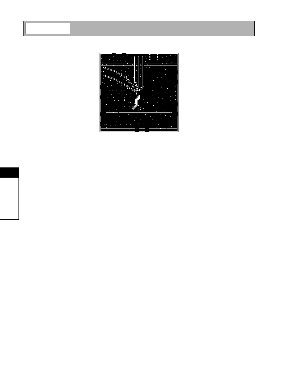
Evaluation Board Layout
Board Size 2.0" x 2.0"
Board Thickness 0.031", Board Material FR-4, Multi-Layer
Assembly
Top
Power Plane 1
Power Plane 2
Preliminary
8-132
RF2461
Rev A13 010607
8
F
R
O
N
T
-
E
NDS
Back
Preliminary
8-133
RF2461
Rev A13 010607
8
F
R
O
N
T
-
E
NDS
Condition T =25
o
C, VCC =2.75 V, RF= 880 and 881MHz, LO = 965MHz @-10 dBm
LNA Current =LNA Gain2-LNA-Gain1
IP_SET
IF_SEL
LNA GAIN
MIX GAIN
ENABLE
MIXER_GAIN
0
0
0
1
1
LNA_GAIN1
1
0
0
0
1
LNA_GAIN2
1
0
1
0
1
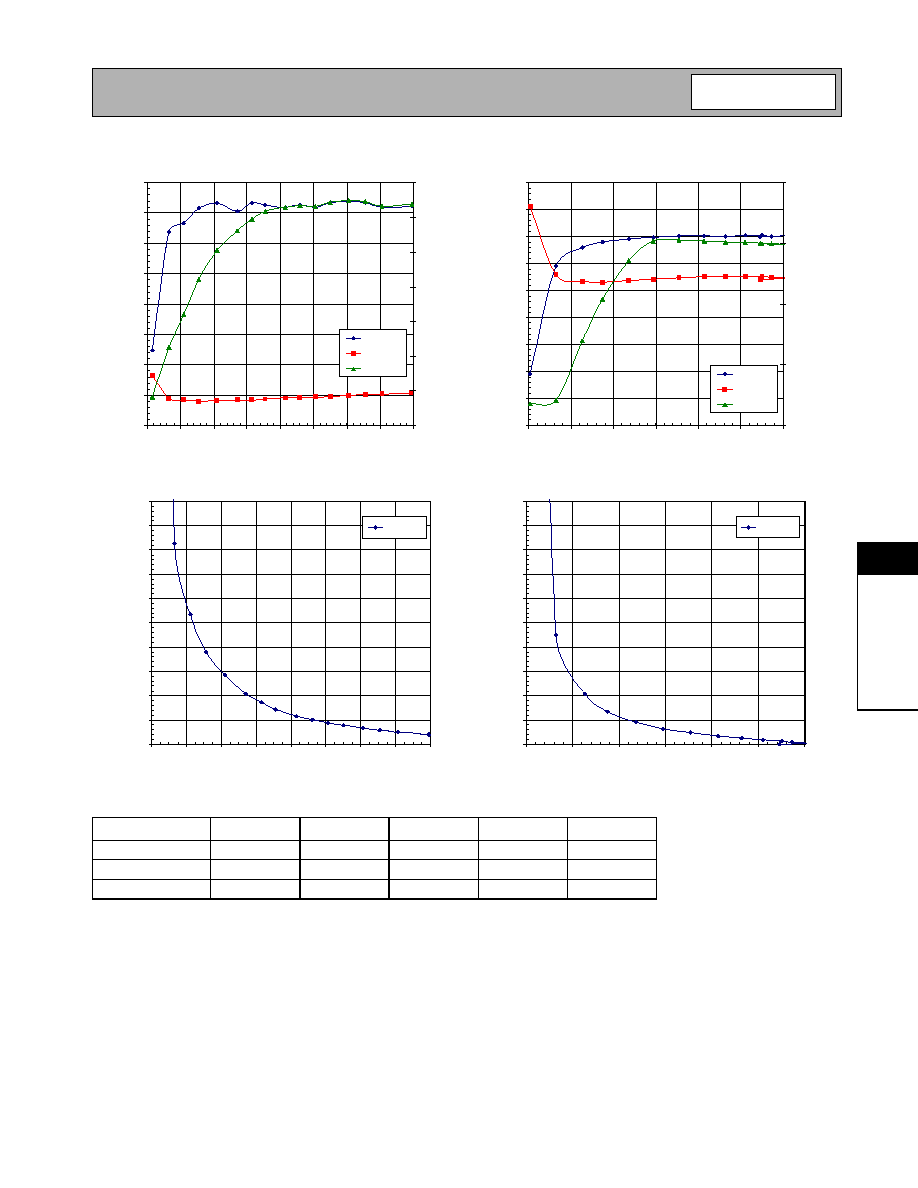
LNA Gain, Noise Figure and IIP3 versus I
CC
-
LNA Only (LNA High Gain)
0.0
2.0
4.0
6.0
8.0
10.0
12.0
14.0
16.0
0.0
2.0
4.0
6.0
8.0
10.0
12.0
14.0
16.0
I
CC
(mA)
Gain
and
Noise
Figure
(
dB)
-20.0
-15.0
-10.0
-5.0
0.0
5.0
10.0
15.0
IIP3
(dBm)
Gain (dB)
NF (dB)
IIP3 (dBm)
Mixer Gain, Noise Figure and IIP3 versus I
CC
-
Mixer (Mixer High Gain, LO=-7dBm)
-20.00
-15.00
-10.00
-5.00
0.00
5.00
10.00
15.00
20.00
25.00
10.00
15.00
20.00
25.00
30.00
35.00
40.00
I
CC
(mA)
Gain
and
Noise
Figure
(
dB)
-10.00
-5.00
0.00
5.00
10.00
IIP3
(dBm)
Gain (dB)
NF (dB)
IIP3 (dBm)
Resistor (R3) versus I
CC
(mA) -
LNA Only (LNA High Gain)
0.0
20.0
40.0
60.0
80.0
100.0
120.0
140.0
160.0
180.0
200.0
0.0
2.0
4.0
6.0
8.0
10.0
12.0
14.0
16.0
I
CC
(mA)
Resistor
R3
(k
)
R3 (kohm)
Resistor (R2) versus I
CC
- Mixer (Mixer High Gain,
LO=2170@-7dBm)
0.0
20.0
40.0
60.0
80.0
100.0
120.0
140.0
160.0
180.0
200.0
10.0
15.0
20.0
25.0
30.0
35.0
40.0
I
CC
(mA)
Resistor
R2
(
k
)
R2 (kohm)
Preliminary
8-134
RF2461
Rev A13 010607
8
F
R
O
N
T
-
E
NDS
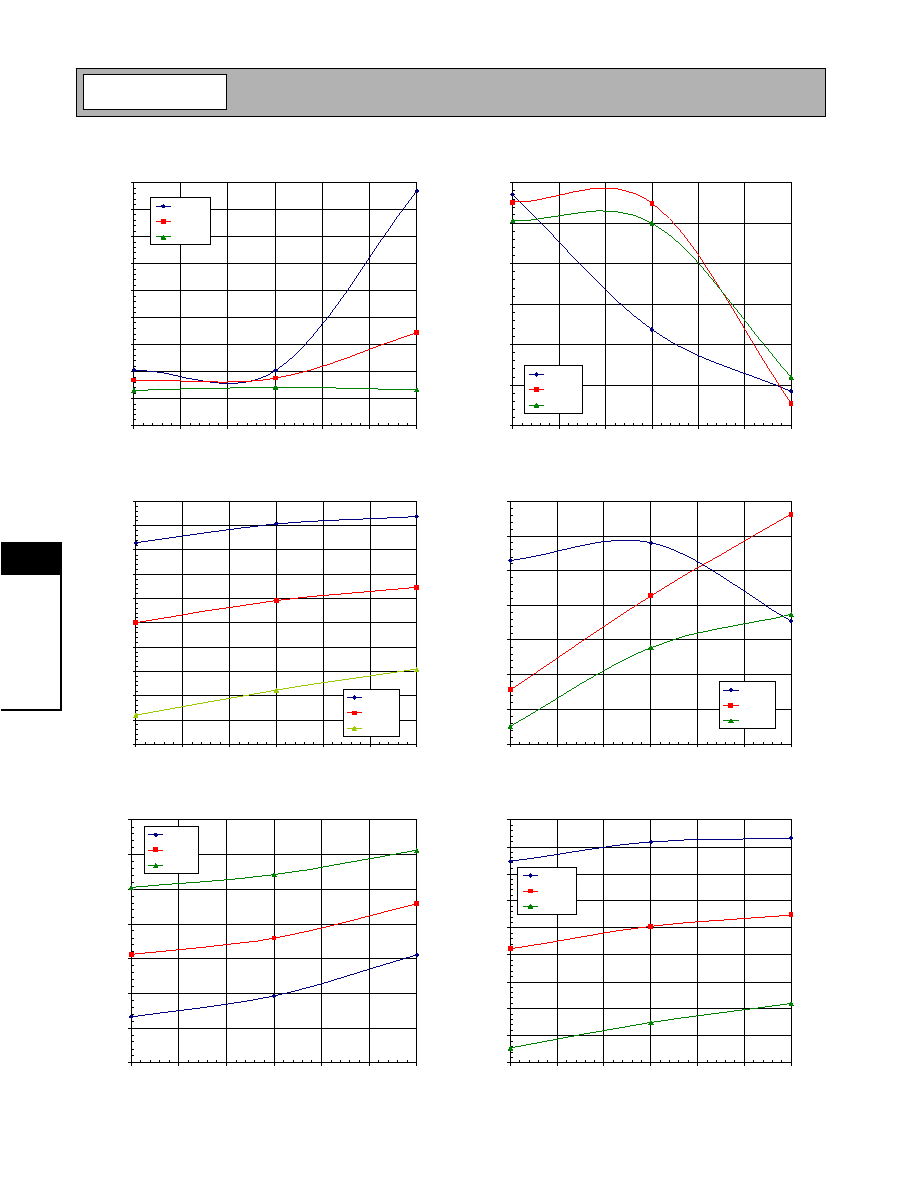
LNA (Low Gain Mode)
-8.00
-7.00
-6.00
-5.00
-4.00
-3.00
-2.00
-1.00
0.00
1.00
2.7
2.8
2.9
3.0
3.1
3.2
3.3
V
CC
(V)
S21
(
dB)
S21, -30∫
S21, 25∫
S21, 85∫
LNA (Low Gain Mode)
-10.00
-5.00
0.00
5.00
10.00
15.00
20.00
2.7
2.8
2.9
3.0
3.1
3.2
3.3
V
CC
(V)
IIP3
(dBm)
IIP3, -30∫
IIP3, 25∫
IIP3, 85∫
LNA (High Gain/Low IP Mode)
14.10
14.20
14.30
14.40
14.50
14.60
14.70
14.80
14.90
15.00
15.10
2.7
2.8
2.9
3.0
3.1
3.2
3.3
V
CC
(V)
S21
(
dB)
S21, -30∫
S21, 25∫
S21, 85∫
LNA (High Gain/Low IP Mode)
7.00
8.00
9.00
10.00
11.00
12.00
13.00
14.00
2.7
2.8
2.9
3.0
3.1
3.2
3.3
V
CC
(V)
IIP3
(dBm)
IIP3, -30∫
IIP3, 25∫
IIP3, 85∫
LNA (High Gain/Low IP Mode)
1.00
1.20
1.40
1.60
1.80
2.00
2.20
2.40
2.7
2.8
2.9
3.0
3.1
3.2
3.3
V
CC
(V)
NF
(dB)
NF, -30∫
NF, 25∫
NF, 85∫
LNA (High Gain/High IP Mode)
14.20
14.30
14.40
14.50
14.60
14.70
14.80
14.90
15.00
15.10
2.7
2.8
2.9
3.0
3.1
3.2
3.3
V
CC
(V)
S21
(
dB)
S21, -30∫
S21, 25∫
S21, 85∫
Preliminary
8-135
RF2461
Rev A13 010607
8
F
R
O
N
T
-
E
NDS
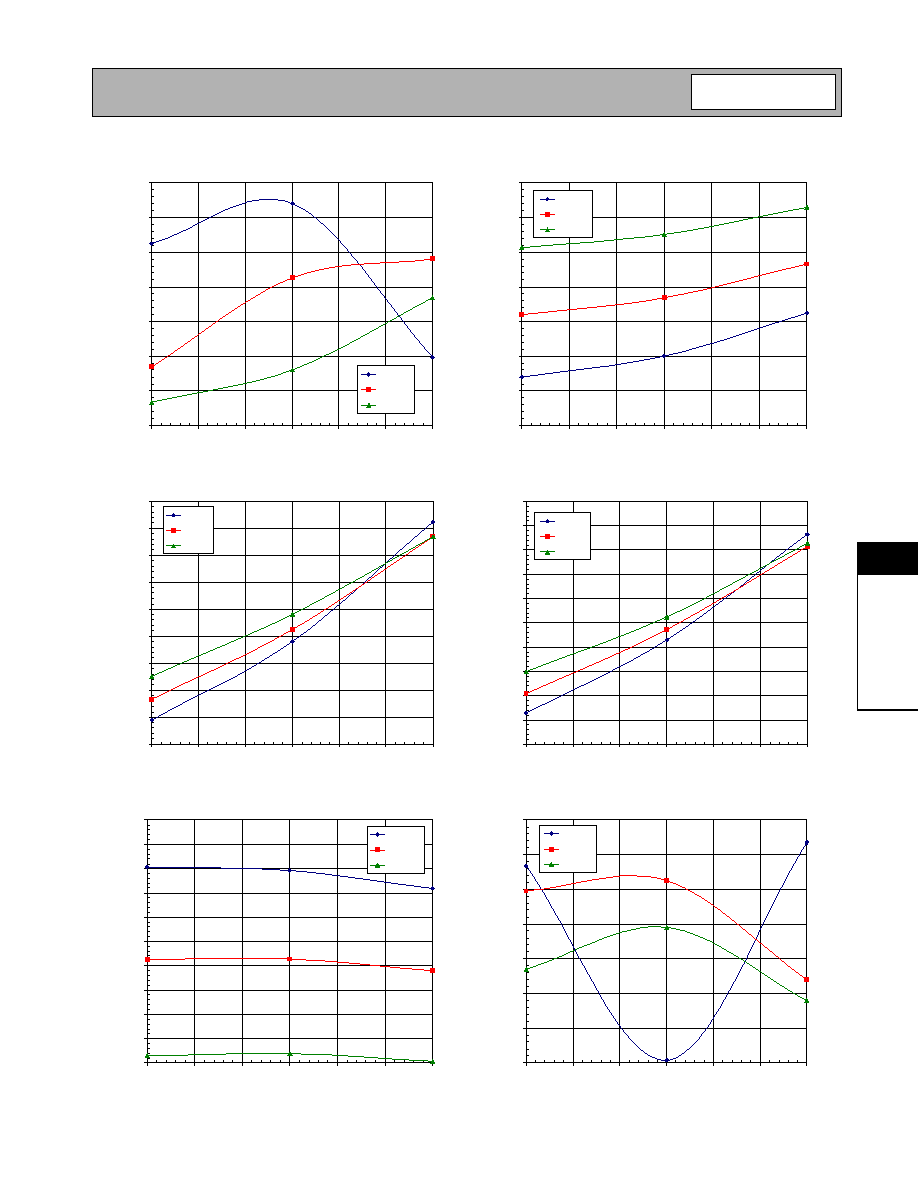
LNA (High Gain/High IP mode)
8.00
9.00
10.00
11.00
12.00
13.00
14.00
15.00
2.7
2.8
2.9
3.0
3.1
3.2
3.3
V
CC
(V)
IIP3
(dBm)
IIP3, -30∫
IIP3, 25∫
IIP3, 85∫
LNA (High Gain/High IP Mode)
1.00
1.20
1.40
1.60
1.80
2.00
2.20
2.40
2.7
2.8
2.9
3.0
3.1
3.2
3.3
V
CC
(V)
NF
(dB)
NF, -30∫
NF, 25∫
NF, 85∫
VCC versus I
CC
, LNA High Mode, Low IP
21.00
21.50
22.00
22.50
23.00
23.50
24.00
24.50
25.00
25.50
2.7
2.8
2.9
3.0
3.1
3.2
3.3
V
CC
(V)
I
CC
(mA)
Icc, -30∫
Icc, 25∫
Icc, 85∫
V
CC
versus I
CC
, LNA High Mode, High IP
21.00
21.50
22.00
22.50
23.00
23.50
24.00
24.50
25.00
25.50
26.00
2.7
2.8
2.9
3.0
3.1
3.2
3.3
V
CC
(V)
I
CC
(mA)
Icc, -30∫
Icc, 25∫
Icc, 85∫
Mixer (IF1), Low Gain Mode, LO@-10dBm
5.00
5.20
5.40
5.60
5.80
6.00
6.20
6.40
6.60
6.80
7.00
2.7
2.8
2.9
3.0
3.1
3.2
3.3
V
CC
(V)
Gain
(dB)
Gain, -30∫
Gain, 25∫
Gain, 85∫
Mixer IF1, Low Gain Mode, LO@-10dBm
12.00
12.50
13.00
13.50
14.00
14.50
15.00
15.50
2.7
2.8
2.9
3.0
3.1
3.2
3.3
V
CC
(V)
IIP3
(dBm)
IIP3, -30∫
IIP3, 25∫
IIP3, 85∫

Preliminary
8-136
RF2461
Rev A13 010607
8
F
R
O
N
T
-
E
NDS
Mixer IF1, Low Gain Mode, LO@-10dBm
10.00
10.50
11.00
11.50
12.00
12.50
13.00
13.50
14.00
2.7
2.8
2.8
2.9
2.9
3.0
3.0
V
CC
(V)
NF
(dB)
NF, -30∫
NF, 25∫
NF, 85∫
Mixer IF1, High Gain Mode, LO@-10dBm
13.50
14.00
14.50
15.00
15.50
16.00
2.7
2.8
2.9
3.0
3.1
3.2
3.3
V
CC
(V)
Gain
(dB)
Gain, -30∫
Gain, 25∫
Gain, 85∫
Mixer IF1, High Gain Mode, LO@-10dBm
2.00
2.50
3.00
3.50
4.00
4.50
5.00
2.7
2.8
2.9
3.0
3.1
3.2
3.3
V
CC
(V)
IIP3
(dBm)
IIP3, -30∫
IIP3, 25∫
IIP3, 85∫
Mixer IF1, High Gain Mode, LO@-10dBm
4.00
4.50
5.00
5.50
6.00
6.50
7.00
7.50
8.00
8.50
2.75
2.80
2.85
2.90
2.95
3.00
V
CC
(V)
NF
(dB)
NF, -30∫
NF, 25∫
NF, 85∫
Mixer IF1, High Gain Mode, V
CC
@2.75V
13.00
13.50
14.00
14.50
15.00
15.50
16.00
-10.0
-8.0
-6.0
-4.0
-2.0
0.0
LO (dBm)
Gain
(dB)
Gain, -30∫
Gain, 25∫
Gain, 85∫
Mixer IF1, High Gain Mode, V
CC
@2.75V
2.00
2.50
3.00
3.50
4.00
4.50
-10.0
-8.0
-6.0
-4.0
-2.0
0.0
LO (dBm)
IIP3
(dBm)
IIP3, -30∫
IIP3, 25∫
IIP3, 85∫