 | –≠–ª–µ–∫—Ç—Ä–æ–Ω–Ω—ã–π –∫–æ–º–ø–æ–Ω–µ–Ω—Ç: RF2492 | –°–∫–∞—á–∞—Ç—å:  PDF PDF  ZIP ZIP |

¸
8-33
8
F
R
O
N
T
-
E
NDS
Preliminary
Product Description
Ordering Information
Typical Applications
Features
Functional Block Diagram
RF Micro Devices, Inc.
7625 Thorndike Road
Greensboro, NC 27409, USA
Tel (336) 664 1233
Fax (336) 664 0454
http://www.rfmd.com
Optimum Technology MatchingÆ Applied
Si BJT
GaAs MESFET
GaAs HBT
Si Bi-CMOS
SiGe HBT
Si CMOS
LNA IP SEL
LNA ISET
X2 ENABLE
BAND SEL
IF SEL
32
31
17
10
9
LOGIC
CONTROL
PCS LNA IN
CELL LNA IN
LNA GAIN SEL
MIX GAIN SEL
11
14
12
30
25
23
4
5
7
8
19
20
21
22
1
18
15
PCS LO OUT -
CELL LO OUT+
CELL LO OUT-
PCS LO OUT+
IF1+
IF2+
IF1-
IF2-
LO
IN
CELL
M
I
X
I
N
CELL
LNA
O
UT
X2
PCS
M
IX
IN
PCS
L
NA
OUT
RF2492
DUAL-BAND LOW NOISE AMPLIFIER/MIXER
∑ TDMA-GSM Cellular/PCS Handsets
∑ TDMA Cellular/PCS Handsets
∑ GAIT Handsets
∑ CDMA Cellular/PCS Handsets
∑ GSM DCS/PCS Handsets
The RF2492 is a fully featured dual-band LNA/Mixer and
is usable in a variety of mobile handset applications. The
unique dual IF outputs provide interface to two indepen-
dent IF SAW filters supporting applications such as
TDMA-EDGE where 30kHz and 200 kHz bandwidth SAW
filters are used. With independent power management
control pins for the LNAs and mixers, either IF output can
be accessed from either high- or low-band LNAs, provid-
ing maximum flexibility with minimum power usage. Multi-
ple gain control options are provided to achieve a very
large dynamic range for the receiver. A frequency doubler
is included in the LO circuit to generate both high- and
low-band LO signals with a single VCO. The RF2492 is
packaged in a 32 pin, 5mmx5mm, leadless plastic pack-
age.
∑ Complete Dual-Band Receiver Front End
∑ Low Noise Figure
∑ Stepped LNA/Mixer Gain Control
∑ Adjustable LNA Bias Current/IIP3
∑ Integrated LO Frequency Doubler
∑ Differential LO Buffer Outputs
RF2492
Dual-Band Low Noise Amplifier/Mixer
RF2492 PCBA
Fully Assembled Evaluation Board
8
Rev A4 010828
1.00
0.85
5.00
sq.
NOTES:
Shaded Pin is Lead 1.
1
Package Warpage: 0.05 mm max.
4
Die Thickness Allowable: 0.305 mm max.
5
Pin 1 identifier must exist on top surface of package by identification
mark or feature on the package body. Exact shape and size is optional.
2
Dimension applies to plated terminal: to be measured between 0.02 mm
and 0.25 mm from terminal end.
3
0.30
0.18
3
0.60
0.24 typ
0.55
0.30
0.50
0.23
0.13
4 PLCS
0.45
0.20
4 PLCS
0.05
0.01
0.80
0.65
3.25
2.95 sq.
12∞
MAX
Package Style: LCC, 32-Pin, 5x5

Preliminary
8-34
RF2492
Rev A4 010828
8
F
R
O
N
T
-
E
NDS
Absolute Maximum Ratings
Parameter
Rating
Unit
Supply Voltage
-0.5 to +5.0
V
DC
Input LO and RF Levels
+6
dBm
Operating Ambient Temperature
-40 to +85
∞C
Storage Temperature
-40 to +150
∞C
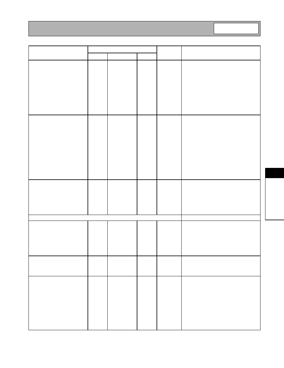
Parameter
Specification
Unit
Condition
Min.
Typ.
Max.
Overall
T = 25∞C, V
CC
=2.75V
RF Frequency Range
881
MHz
Specifications
1960
MHz
Specifications
800
950
MHz
Usable range
1700
2100
MHz
Usable range
IF Frequency Range
110
MHz
Specifications
50
250
MHz
Usable range
Cell LO Buffer Output
-13.0
-12.7
dBm
T1 insertion loss not considered.
PCS LO Buffer Output
-14.0
-12.7
dBm
T2 insertion loss not considered.
Cellular Band
Freq= 869MHz to 894MHz
LNA (On)
RF= 880MHz and 881MHz
Gain
13.5
14.5
15.5
dB
LNA set for max IIP3
13.5
14
15
dB
LNA set for Nominal IIP3
Noise Figure
2.0
2.2
dB
LNA set for max IIP3
1.8
2.0
dB
LNA set for Nominal IIP3
Input IP3
+7.0
+7.5
dBm
LNA set for max IIP3
+1.5
+3.0
+7.0
dBm
LNA set for Nominal IIP3
LNA (Off)
Gain
-8.5
-7.5
-6.5
dB
Noise Figure
5.5
5.8
6.0
dB
Input IP3
+20.0
+21.0
dBm
Mixer
IF Select= 1, (IF1) RF = 880MHz,
LO= 990MHz@-5dBm
Gain
12
13
14
dB
Mixer RF amp ON;
Z
LOAD
=1k
single-ended
3.5
4.4
5.0
dB
Mixer RF amp OFF
Noise Figure
6.5
7.0
7.5
dB
Mixer RF amp ON
13.5
14.0
14.5
dB
Mixer RF amp OFF
Input IP3
+2.0
+4.5
dBm
Mixer RF amp ON
+11.5
+13.8
dBm
Mixer RF amp OFF
LO Input Level
-5
dBm
Specifications
-10
+3
dBm
Usable range
Mixer
IF Select= 0, (IF2) RF = 880MHz,
LO= 990MHz@-5dBm
Gain
12
13
14
dB
Mixer RF amp ON;
Z
LOAD
=1k
single-ended
3.0
4.4
dB
Mixer RF amp OFF
Noise Figure
6.8
7.2
7.4
dB
Mixer RF amp ON
13.7
14.0
14.2
dB
Mixer RF amp OFF
Input IP3
+2.0
+4.5
dBm
Mixer RF amp ON
+11.5
+14.0
dBm
Mixer RF amp OFF
LO Input Level
-5
dBm
Specifications
-10
+3
dBm
Usable range
Caution! ESD sensitive device.
RF Micro Devices believes the furnished information is correct and accurate
at the time of this printing. However, RF Micro Devices reserves the right to
make changes to its products without notice. RF Micro Devices does not
assume responsibility for the use of the described product(s).
Preliminary
8-35
RF2492
Rev A4 010828
8
F
R
O
N
T
-
E
NDS
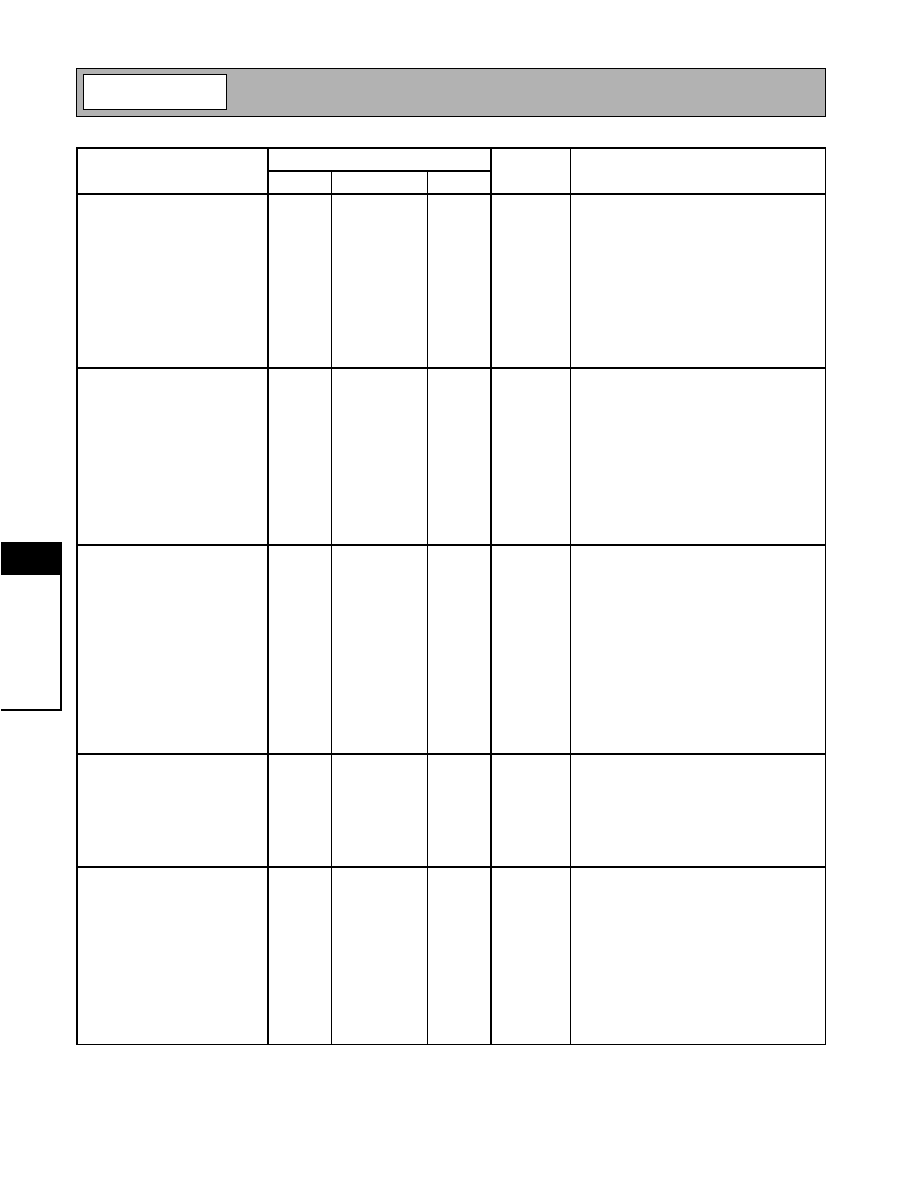
Parameter
Specification
Unit
Condition
Min.
Typ.
Max.
Mixer Isolation
LO to RF
40
42
dB
Mixer RF amp ON
LO to RF
33.5
35
dB
Mixer RF amp OFF
RF to LO
56.5
63
dB
Mixer RF amp ON
RF to LO
54.5
60.5
dB
Mixer RF amp OFF
LO to IF1
24
36.5
dB
Mixer RF amp ON
LO to IF2
28
42
dB
Mixer RF amp ON
IF1 to RF
50
51
dB
Mixer RF amp ON
RF to IF1
43.5
44.5
dB
Mixer RF amp ON
IF2 to RF
49.5
50.5
dB
Mixer RF amp ON
RF to IF2
43
45
dB
Mixer RF amp ON
Cascade (LNA On)
IF Select= 1, 3dB RF Filter Insertion Loss
Gain
24.5
dB
LNA set for max IIP3; Mixer RF amp ON
24
dB
LNA set for Nominal IIP3; Mixer RF amp ON
15.9
dB
LNA set for max IIP3; Mixer RF amp OFF
15.4
dB
LNA set for Nominal IIP3; Mixer RF ampOFF
Noise Figure
2.8
dB
LNA set for max IIP3; Mixer RF amp ON
2.7
dB
LNA set for Nominal IIP3; Mixer RF amp ON
5.3
dB
LNA set for max IIP3; Mixer RF amp OFF
5.4
dB
LNA set for Nominal IIP3; Mixer RF ampOFF
Input IP3
-6.5
dBm
LNA set for max IIP3; Mixer RF amp ON
-6.4
dBm
LNA set for Nominal IIP3; Mixer RF amp ON
+1.1
dBm
LNA set for max IIP3; Mixer RF amp OFF
0
dBm
LNA set for Nominal IIP3; Mixer RF ampOFF
Cascade (LNA Off)
IF Select= 1, 3dB RF Filter Insertion Loss
Gain
2.5
dB
Mixer RF amp ON
-6.0
dB
Mixer RF amp OFF
Noise Figure
17.4
dB
Mixer RF amp ON
24.5
dB
Mixer RF amp OFF
Input IP3
+14.5
dBm
Mixer RF amp ON
+19.0
dBm
Mixer RF amp OFF
PCS Band
Freq= 1930MHz to 1990MHz
LNA (On)
RF = 1960MHz and 1961MHz
Gain
13.0
14.8
dB
LNA set for max IIP3
13.0
14.0
dB
LNA set for Nominal IIP3
Noise Figure
1.5
1.9
dB
LNA set for max IIP3
1.7
1.8
1.9
dB
LNA set for Nominal IIP3
Input IP3
+7.0
+9.0
dBm
LNA set for max IIP3
+0.5
+3.5
dBm
LNA set for Nominal IIP3
LNA (Off)
Gain
-7.0
-5.5
dB
Noise Figure
6.0
6.2
6.5
dB
Input IP3
+20.0
+25.0
dBm
Mixer
RF = 1960MHz, LO= 1035MHz@ -5dBm,
IF Select= 1 (IF1)
Gain
11.5
12.5
dB
Mixer RF amp ON;
Z
LOAD
=1k
single-ended
2.0
3.5
dB
Mixer RF amp OFF
Noise Figure
8.0
8.5
9.0
dB
Mixer RF amp ON
15.0
15.5
16.0
dB
Mixer RF amp OFF
Input IP3
+4.0
+6.0
dBm
Mixer RF amp ON
+14.0
+16.0
dBm
Mixer RF amp OFF
LO Input Level
-5
dBm
Specifications
-10
+3
dBm
Usable range
Preliminary
8-36
RF2492
Rev A4 010828
8
F
R
O
N
T
-
E
NDS
Parameter
Specification
Unit
Condition
Min.
Typ.
Max.
Mixer
RF= 1960MHz, LO =1035MHz@-5dBm,
IF Select=0 (IF2)
Gain
11.0
12.6
dB
Mixer RF amp ON;
Z
LOAD
=1k
single-ended
2.0
3.5
dB
Mixer RF amp OFF
Noise Figure
8.0
8.4
9.0
dB
Mixer RF amp ON
15.0
15.5
16.5
dB
Mixer RF amp OFF
Input IP3
+3.5
+6.0
dBm
Mixer RF amp ON
+14.0
+16.0
dBm
Mixer RF amp OFF
LO Input Level
-5
dBm
Specifications
-10
+3
dBm
Usable range
Mixer Isolation
LO to RF
55
57.5
dB
Mixer RF amp ON
LO to RF
54
63
dB
Mixer RF amp OFF
RF to LO
49.8
52.5
dB
Mixer RF amp ON
RF to LO
52
55.5
dB
Mixer RF amp OFF
LO to IF1
54.5
55.5
dB
Mixer RF amp ON
LO to IF2
58.5
59
dB
Mixer RF amp ON
IF1 to RF
49.5
51
dB
Mixer RF amp ON
RF to IF1
33
34.5
dB
Mixer RF amp ON
IF2 to RF
49
50.5
dB
Mixer RF amp ON
RF to IF2
41
42.5
dB
Mixer RF amp ON
Cascade (LNA On)
3dB RF Filter Insertion Loss
Gain
24.3
dB
LNA set for max IIP3; Mixer RF amp ON
23.5
dB
LNA set for Nominal IIP3; Mixer RF amp ON
15.3
dB
LNA set for max IIP3; Mixer RF amp OFF
14.5
dB
LNA set for Nominal IIP3; Mixer RF ampOFF
Noise Figure
2.6
dB
LNA set for max IIP3; Mixer RF amp ON
3.1
dB
LNA set for Nominal IIP3; Mixer RF amp ON
5.7
dB
LNA set for max IIP3; Mixer RF amp OFF
6.3
dB
LNA set for Nominal IIP3; Mixer RF ampOFF
Input IP3
-6
dBm
LNA set for max IIP3; Mixer RF amp ON
-5.6
dBm
LNA set for Nominal IIP3; Mixer RF amp ON
+3.0
dBm
LNA set for max IIP3; Mixer RF amp OFF
+1.5
dBm
LNA set for Nominal IIP3; Mixer RF ampOFF
Cascade (LNA Off)
3dB RF Filter Insertion Loss
Gain
4
dB
Mixer RF amp ON
-5
dB
Mixer RF amp OFF
Noise Figure
17
dB
Mixer RF amp ON
24
dB
Mixer RF amp OFF
Input IP3
+14.0
dBm
Mixer RF amp ON
+21.7
dBm
Mixer RF amp OFF
Power Supply
IF Select=1
Supply Voltage
2.75
V
Specifications
2.7
3.6
V
Operating range
Supply Current
38
40
mA
Cellular; LNA On, Max IIP3,Mixer RFampON
36
38
mA
Cellular;LNAOn,NomIIP3,Mixer RFamp ON
32
34
mA
Cellular; LNA Off, Mixer RF amp ON
26
28
mA
Cellular; LNA Off, Mixer RF amp OFF
LNA Current
40.0
42.5
mA
PCS; LNA On, Max IIP3, Mixer RF amp ON
38.5
40.5
mA
PCS; LNA On, Nom IIP3, Mixer RF amp ON
34.5
36.0
mA
PCS; LNA Off, Mixer RF amp ON
28.0
29.5
mA
PCS; LNA Off, Mixer RF amp OFF

Preliminary
8-37
RF2492
Rev A4 010828
8
F
R
O
N
T
-
E
NDS
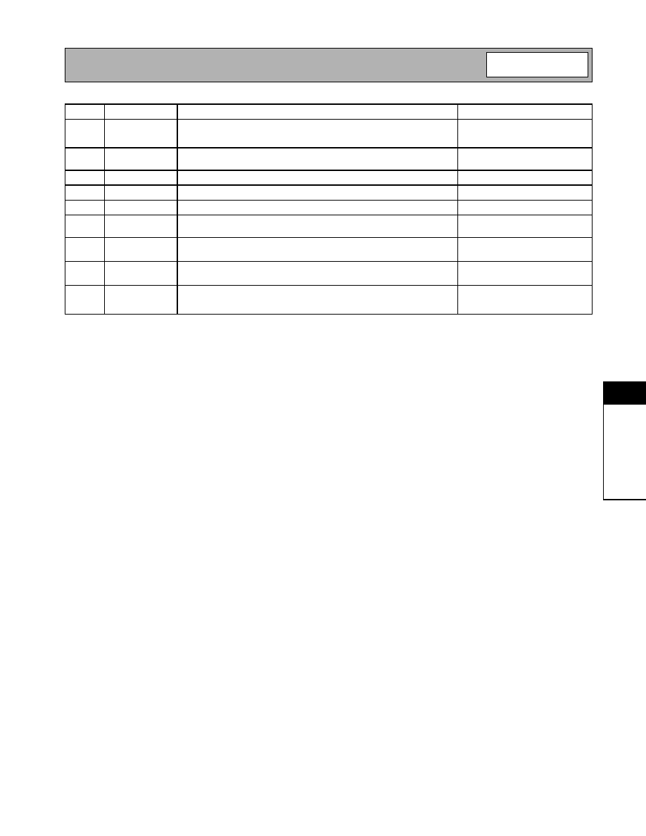
State Table (Typical Values for V
CC
=2.75V and 3dB RF Filter Insertion Loss)
Control Logic Table
Parameter
Cellular
PCS
LNA On
LNA Off
LNA On
LNA Off
LNA at Max IIP3 LNA at Nom IIP3
LNA at Max IIP3 LNA at Nom IIP3
Mixer
Amp On
Mixer
Amp Off
Mixer
Amp On
Mixer
Amp Off
Mixer
Amp On
Mixer
Amp Off
Mixer
Amp On
Mixer
Amp Off
Mixer
Amp On
Mixer
Amp Off
Mixer
Amp On
Mixer
Amp Off
Cascade
Gain (dB)
24.5
15.9
24
15.4
2
-6.8
24.3
15.3
23.5
14.5
4
-5
Noise Figure (dB)
2.8
5.3
2.7
5.4
18.2
25.2
2.6
5.7
3.1
6.3
17
24
Input IP3 (dBm)
-6.5
+1.1
-6.4
0
+14.9
+19.5
-6
+3
-5.6
+1.5
+14
+21.7
Total Current
38
36
32
26
40
38.5
34.5
28
LNA
Gain (dB)
14.5
14.5
14
14
-7.5
-7.5
14.8
14.8
14
14
-5.5
-5.5
Noise Figure (dB)
2.0
2.0
1.8
1.8
5.8
5.8
1.5
1.5
1.8
1.8
6.2
6.2
Input IP3 (dBm)
+7.5
+7.5
+3
+3
+21
+21
+9
+9
+3.5
+3.5
25
25
Isolation (dB)
LNA Current (mA)
Mixer
Gain (dB)
13
4.4
13
4.4
13
4.4
12.5
3.5
12.5
3.5
12.5
3.5
Noise Figure (dB)
7
14
7
14
7
14
8.5
15.5
8.5
15.5
8.5
15.5
Input IP3 (dBm)
+5.1
+13.8
+5.1
+13.8
+5.1
+13.8
+6
+16
+6
+16
+6
+16
LO Input Level (dBm)
-5
-5
-5
-5
-5
-5
-5
-5
-5
-5
-5
-5
LO to RF Isolation(dB)
Mixer Current (mA)
BAND SEL
IF SEL
LNA GAIN
MIX GAIN
LNA IP SEL
ENABLE
PCS IF2 High Gain/High
Linearity
1
0
1
1
1
1
PCS IF2 High Gain/Nomi-
nal Linearity
1
0
1
1
0
1
PCS IF2 Mid1 Gain
1
0
1
0
0
1
PCS IF2 Mid2 Gain
1
0
0
1
0
1
PCS IF2 Low Gain
1
0
0
0
0
1
Cell IF2 High Gain/
High Linearity
0
0
1
1
1
1
Cell IF2 High Gain/Nomi-
nal Linearity
0
0
1
1
0
1
Cell IF2 Mid1 Gain
0
0
1
0
0
1
Cell IF2 Mid2 Gain
0
0
0
1
0
1
Cell IF2 Low Gain
0
0
0
0
0
1
Cell IF1 High Gain/
High Linearity
0
1
1
1
1
1
Cell IF1 High Gain/
Nominal Linearity
0
1
1
1
0
1
Cell IF1 Mid1 Gain
0
1
1
0
0
1
Cell IF1 Mid2 Gain
0
1
0
1
0
1
Cell IF1 Low Gain
0
1
0
0
0
1
Shutdown
X
X
X
X
X
0
Not Defined
1
1
X
X
X
1

Preliminary
8-38
RF2492
Rev A4 010828
8
F
R
O
N
T
-
E
NDS
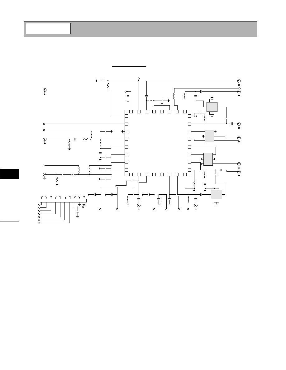
Pin
Function
Description
Interface Schematic
1
LO IN
LO input for both bands. Impedance is approximately (120-j25)
.
1k
shunt resistor (static bleed).
AC coupled to transistor base
(internal DC block).
2
VCC2
Power supply connection for internal LO amplifiers. External low-induc-
tance bypass capacitor between 1nF and 47nF recommended.
3
GND
Ground connection.
4
IF1+
High-band IF output. Open collector. "Current combiner" IF interface to
1000
SAW filter recommended
2pF internal shunt capacitance.
5
IF1-
High-band IF output. Open collector. "Current combiner" IF interface to
1000
SAW filter recommended
2pF internal shunt capacitance.
6
BYPASS
Pin requires external bypass capacitor between 1nF and 47nF.
7
IF2-
Low-band IF output. Open collector. "Current combiner" IF interface to
1000
SAW filter recommended
2pF internal shunt capacitance.
8
IF2+
Low-band IF output. Open collector. "Current combiner" IF interface to
1000
SAW filter recommended
2pF internal shunt capacitance.
9
IF SEL
Logic input. High selects IF1 mixer; low selects IF2 mixer.
Diode to V
CC
and Ground.
CMOS logic interface.
10
LNA IP SEL
Logic input. High selects external LNA current reference (pin 17); low
selects internal LNA current reference.
Diode to V
CC
and Ground.
CMOS logic interface.
11
CELL LNA
IN
Low-band LNA input (base). Simple external matching required for best
performance.
12
LNA GAIN
SEL
Logic input. High selects maximum LNA gain; low selects minimum
LNA gain.
Diode to V
CC
and Ground.
CMOS logic interface.
13
VCC1
Power supply for internal references, logic, and mixer preamplifiers.
Internal RF bypass capacitor. External bypass capacitor between 1nF
and 47nF required.
14
MIX GAIN
SEL
Logic input. High selects maximum mixer gain (mixer RF amp on); low
selects minimum mixer gain (mixer RF amp off).
Diode to V
CC
and Ground.
CMOS logic interface.
15
CELL LNA
OUT
Low-band LNA output (collector). Simple external L-C matching
required.
16
GND
Ground connection. See evaluation board layout.
17
LNA ISET
External current reference for LNA. Resistor to ground sets LNA cur-
rent when Pin 10 is high. 20k
results in approximately 10mA LNA cur-
rent. Higher resistance results in lower current.
18
CELL MIX
IN
Low band mixer RF preamplifier input (base). External L-C network
required for best performance.
19
PCS LO
OUT+
High-band buffered LO output.
Internal DC blocking capacitor.
1k
shunt resistor (static bleed).
20
PCS LO
OUT-
High-band buffered LO output.
Internal DC blocking capacitor.
1k
shunt resistor (static bleed).
21
CELL LO
OUT+
Low-band buffered LO output.
Internal DC blocking capacitor.
1k
shunt resistor (static bleed).
22
CELL LO
OUT-
Low-band buffered LO output.
Internal DC blocking capacitor.
1k
shunt resistor (static bleed).
23
PCS MIX IN
High-band mixer RF preamplifier input (base). External L-C network
required for best performance.
24
GND
Ground connection. Keep traces physically short and connect immedi-
ately to ground plane (low-inductance ground required for best perfor-
mance).
Preliminary
8-39
RF2492
Rev A4 010828
8
F
R
O
N
T
-
E
NDS
Pin
Function
Description
Interface Schematic
25
PCS LNA
OUT
High-band LNA output (collector). Small external inductance required
for best impedance match to 50
.
26
VCC2
High-band LNA power supply connection. Small series inductance
required.
27
GND2
High-band LNA emitter. Low-inductance ground required.
28
GND2
Same as pin 27.
29
GND2
Same as pin 27.
30
PCS LNA IN
High-band LNA input (base). Simple external matching required for
best performance.
31
BAND SEL
Logic input. High selects high-band operation; low selects low-band
operation.
Diode to V
CC
and Ground.
CMOS logic interface.
32
X2 ENABLE
Logic input. High enables LO doubler; low disables LO doubler.
Diode to V
CC
and Ground.
CMOS logic interface.
Die
Flag
GND
Low inductance ground connection critical to proper operation.

Preliminary
8-40
RF2492
Rev A4 010828
8
F
R
O
N
T
-
E
NDS
Pin Out
1
3
6
4
5
2
9
14
10
13
11
12
32
27
31
28
30
29
24
22
19
21
20
23
26
25
7
8
15
16
18
17
LO IN
VCC2
GND
IF1+
IF1-
BYPASS
IF2-
IF2+
IF
SE
L
LNA
I
P
S
E
L
CE
LL
LN
A
I
N
LN
A
G
A
I
N
S
E
L
VC
C1
MIX
G
A
I
N
S
EL
CE
L
L
L
N
A
O
UT
GN
D
LNA ISET
CELL MIX IN
PCS LO OUT+
PCS OUT-
CELL LO OUT+
CELL LO OUT-
PCS MIX IN
GND
PC
S
L
NA
O
U
T
VC
C2
GN
D
2
GN
D
2
GN
D
2
PC
S
L
NA
I
N
BA
ND
S
E
L
X2
EN
AB
L
E

Preliminary
8-41
RF2492
Rev A4 010828
8
F
R
O
N
T
-
E
NDS
Application Schematic
1
3
6
4
5
2
9
14
10
13
11
12
32
27
31
28
30
29
24
22
19
21
20
23
26
25
7
8
15
16
18
17
33 nF
X2 ENABLE
BAND SEL
120
47 nH
C2
33 nF
36 nH
2.2 nH
33 nF
47 nH
C1
20 pF
33 nF
180 nH
18 pF
270 nH
8 pF
20 pF
180 nH
18 pF
270 nH
8 pF
33 nF
LNA GAIN
C2
33 nF
IN
OUT
GN
D
G
N
D
GN
D
G
N
D
7.5 nH
IP SET
IF SEL
2
1
4
3
6
5
C1
F1
47 nH
C1
IN
OUT
GN
D
G
N
D
GN
D
G
N
D
33 nF
F2
4
1
5
2
6
3
27 k
4 pF
5.6 nH
MIX GAIN
VCO L OUT N
VCO L OUT P
VCO H OUT N
VCO H OUT P
V
CC
LNA H IN
LO IN
V
CC
V
CC
IF1 OUT
V
CC
IF2 OUT
LNA L IN
V
CC
V
CC
4 pF
LNA L OUT
33 pF
NOTES:
1. C1's are not needed if filter DC impedance is open circuit (as is normally the case).
2. C2's are not needed if duplexer DC impedance is open circuit (as is normally the case).
3. IF interface shown is 50
@ 110 MHz.
Preliminary
8-42
RF2492
Rev A4 010828
8
F
R
O
N
T
-
E
NDS
Evaluation Board Schematic
IF=110MHz
(Download Bill of Materials from www.rfmd.com.)
1
3
6
4
5
2
9
14
10
13
11
12
32
27
31
28
30
29
24
22
19
21
20
23
26
25
7
8
15
16
18
17
J1
LO IN
C27
33 nF
X2 ENABLE
BAND SEL
C28
33 nF
R1
120
VCC
L13
47 nH
C26
33 nF
C25
33 nF
J11
LNA H IN
L12
36 nH
VCC
L11
2.2 nH
C23
33 nF
J10
LNA H OUT
C22
33 nF
L8
47 nH
C24
DNI
C3
20 pF
C4
33 nF
L1
180 nH
C1
18 pF
L2
270 nH
R2
0
C2
8 pF
VCC
R3
DNI
J2
IF1 OUT
C5
20 pF
L3
180 nH
C7
18 pF
L4
270 nH
VCC
R4
0
C6
8 pF
R5
DNI
J3
IF2 OUT
C13
33 nF
VCC
LNA GAIN
C11
33 nF
J4
LNA L IN
C10
33 nF
IN
OUT
GN
D
G
N
D
GN
D
G
N
D
L5
7.5 nH
C9
33 nF
IP SET
C8
33 nF
IF SEL
2
1
4
3
6
5
C21
DNI
C20
33 nF
J9
MIX H IN
F1
1
5
2
3
6
4
J8
LO L OUT
IN
GND
GND
OUT
IN
GND
IN
IN
GND
GND
GND
IN
T1
6
5
4
2
1
3
T2
J7
LO H OUT
L7
47 nH
C18
DNI
J6
MIX L IN
IN
OUT
GN
D
G
N
D
GN
D
G
N
D
C17
33 nF
F2
4
1
5
2
6
3
R6
27 k
C12
33 nF
C16
DNI
L6
5.6 nH
C15
4 pF
J5
LNA L OUT
VCC
C14
33 nF
MIX GAIN
P1
1
2
3
4
5
6
7
8
9
10 CON10
P1-8
GN
D
P1-1
GN
D
P1-7
P1-6
P1-5
P1-4
P1-3
P1-2
VC
C
X2
E
N
AB
LE
BA
ND
SE
L
IP
S
E
T
IF
S
E
L
LN
A
G
AI
N
MI
X
G
AI
N
NC
C29
1 uF
+
636.6 pS Delay
0.20 dB Line Loss
460.0 pS Delay
0.02 dB Line Loss
522.7 pS Delay
0.03 dB Line Loss
629.8 pS Delay
0.17 dB Line Loss
592.7 pS Delay
0.15 dB Line Loss
644.7 pS Delay
0.17 dB Line Loss
C19
33 nF
442.2 pS Delay
0.28 dB Line Loss
421.3 pS Delay
0.11 dB Line Loss
605.0 pS Delay
0.40 dB Line Loss
637.6 pS Delay
0.45 dB Line Loss
633.0 pS Delay
0.45 dB Line Loss
NOTE: T1 and T2 approximate insertion loss is ~2 dB.

Preliminary
8-43
RF2492
Rev A4 010828
8
F
R
O
N
T
-
E
NDS
Evaluation Board Layout
Board Size 3.0" x 3.0"
Board Thickness 0.0616", Board Material FR-4, Multi-Layer
Assembly

Preliminary
8-44
RF2492
Rev A4 010828
8
F
R
O
N
T
-
E
NDS
Top
Typical Inner Layer

Preliminary
8-45
RF2492
Rev A4 010828
8
F
R
O
N
T
-
E
NDS
Back

Preliminary
8-46
RF2492
Rev A4 010828
8
F
R
O
N
T
-
E
NDS
LNA Low Band Gain, Noise Figure and IIP3 versus I
CC
LNA Only (LNA High Gain)
-10.0
-5.0
0.0
5.0
10.0
15.0
20.0
2.0
4.0
6.0
8.0
10.0
12.0
I
CC
(mA)
Gain
(dB)
and
IIP3
(dBm)
0.0
0.5
1.0
1.5
2.0
2.5
3.0
Noise
Figure
(
dB)
Gain (dB)
IIP3 (dBm)
NF (dB)
Resistor (R6) versus ICC (mA)
LNA Low Band Only (LNA High Gain)
0.0
10.0
20.0
30.0
40.0
50.0
60.0
70.0
80.0
90.0
100.0
2.00
4.00
6.00
8.00
10.00
12.00
I
CC
(mA)
R6
(k
)
LNA High Band Gain, Noise Figure and IIP3 versus I
CC
LNA Only (LNA High Gain)
-10.00
-5.00
0.00
5.00
10.00
15.00
20.00
2.00
4.00
6.00
8.00
10.00
12.00
I
CC
(mA)
Gain
(dB)
and
IIP3
(dBm)
1.30
1.35
1.40
1.45
1.50
1.55
1.60
1.65
Noise
Figure
(
dB)
Gain (dB)
IIP3 (dBm)
NF (dB)
Resistor (R6) versus I
CC
(mA)
LNA High Band Only (LNA High Gain)
0.0
10.0
20.0
30.0
40.0
50.0
60.0
70.0
80.0
90.0
100.0
2.0
4.0
6.0
8.0
10.0
12.0
I
CC
(mA)
R6
(k
)
Preliminary
8-47
RF2492
Rev A4 010828
8
F
R
O
N
T
-
E
NDS
LNA Cellular Band
(Low Gain Mode)
-8.3
-8.2
-8.1
-8.0
-7.9
-7.8
-7.7
-7.6
-7.5
-7.4
2.7
2.8
2.9
3.0
3.1
3.2
3.3
V
CC
(V)
Gain
(dB)
Gain, -30∫
Gain, 25∫
Gain, 85∫
LNA Cellular Band
(Low Gain Mode)
15.0
16.0
17.0
18.0
19.0
20.0
21.0
22.0
2.7
2.8
2.9
3.0
3.1
3.2
3.3
V
CC
(V)
IIP3
(dBm)
IIP3, -30∫
IIP3, 25∫
IIP3, 85∫
LNA Cellular Band
(High Gain/Nominal IP Mode)
13.4
13.5
13.6
13.7
13.8
13.9
14.0
14.1
14.2
14.3
14.4
2.7
2.8
2.9
3.0
3.1
3.2
3.3
V
CC
(V)
Gain
(dB)
Gain, -30∫
Gain, 25∫
Gain, 85∫
LNA Cellular Band
(High Gain/Nominal IP Mode)
2.0
2.5
3.0
3.5
4.0
4.5
5.0
5.5
6.0
2.7
2.8
2.9
3.0
3.1
3.2
3.3
V
CC
(V)
IIP3
(dBm)
IIP3, -30∫
IIP3, 25∫
IIP3, 85∫
LNA Cellular Band
(High Gain/Nominal IP Mode)
1.0
1.2
1.4
1.6
1.8
2.0
2.2
2.4
2.7
2.8
2.9
3.0
3.1
3.2
3.3
V
CC
(V)
Noise
Figure
(
dB)
NF, -30∫
NF, 25∫
NF, 85∫
LNA Cellular Band
(High Gain/Max IP Mode)
14.0
14.1
14.2
14.3
14.4
14.5
14.6
14.7
14.8
14.9
2.7
2.8
2.9
3.0
3.1
3.2
3.3
V
CC
(V)
Gain
(dB)
Gain, -30∫
Gain, 25∫
Gain, 85∫
Preliminary
8-48
RF2492
Rev A4 010828
8
F
R
O
N
T
-
E
NDS
LNA Cellular Band
(High Gain/Max IP Mode)
6.0
6.5
7.0
7.5
8.0
8.5
2.7
2.8
2.9
3.0
3.1
3.2
3.3
V
CC
(V)
IIP3
(dBm)
IIP3, -30∫
IIP3, 25∫
IIP3, 85∫
LNA Cellular Band
(High Gain/Max IP Mode)
1.0
1.2
1.4
1.6
1.8
2.0
2.2
2.4
2.6
2.7
2.8
2.9
3.0
3.1
3.2
3.3
V
CC
(V)
Noise
Figure
(
dB)
NF, -30∫
NF, 25∫
NF, 85∫
LNA Cellular Band
(High Gain/Nominal IP Mode)
4.00
4.05
4.10
4.15
4.20
4.25
4.30
4.35
4.40
4.45
4.50
2.70
2.80
2.90
3.00
3.10
3.20
3.30
V
CC
(V)
I
CC
(mA)
Icc, -30∫
Icc, 25∫
Icc, 85∫
LNA Cellular Band
(High Gain /Max IP Mode)
5.95
6.00
6.05
6.10
6.15
6.20
6.25
6.30
6.35
6.40
2.70
2.80
2.90
3.00
3.10
3.20
3.30
V
CC
(V)
I
CC
(mA)
Icc, -30∫
Icc, 25∫
Icc, 85∫
Preliminary
8-49
RF2492
Rev A4 010828
8
F
R
O
N
T
-
E
NDS
Cellular Band, Mixer IF1, Low Gain Mode,
LO @ -5 dBm
4.00
4.20
4.40
4.60
4.80
5.00
5.20
5.40
5.60
5.80
2.75
2.85
2.95
3.05
3.15
3.25
3.35
V
CC
(V)
Gain
(dB)
Gain, -30∫
Gain, 25∫
Gain, 85∫
Cellular Band, Mixer IF1, Low Gain Mode,
LO @ -5 dBm
13.00
13.50
14.00
14.50
15.00
15.50
16.00
16.50
2.75
2.85
2.95
3.05
3.15
3.25
3.35
V
CC
(V)
IIP3
(dBm)
IIP3, -30∫
IIP3, 25∫
IIP3, 85∫
Cellular Band, Mixer IF1, Low Gain Mode,
LO @ -5 dBm
10.00
10.50
11.00
11.50
12.00
12.50
13.00
13.50
14.00
2.75
2.80
2.85
2.90
2.95
3.00
V
CC
(V)
Noise
Figure
(
dB)
NF, -30∫
NF, 25∫
NF, 85∫
Cellular Band, Mixer IF1, High Gain Mode,
LO @ -5 dBm
12.50
13.00
13.50
14.00
14.50
15.00
2.75
2.85
2.95
3.05
3.15
3.25
3.35
V
CC
(V)
Gain
(dB)
Gain, -30∫
Gain, 25∫
Gain, 85∫
Cellular Band, Mixer IF1, High Gain Mode,
LO @ -5 dBm
5.00
5.50
6.00
6.50
7.00
7.50
8.00
8.50
9.00
2.75
2.85
2.95
3.05
3.15
3.25
3.35
V
CC
(V)
IIP3
(dBm)
IIP3, -30∫
IIP3, 25∫
IIP3, 85∫
Cellular Band, Mixer IF1, High Gain Mode,
LO @ -5 dBm
6.00
6.50
7.00
7.50
8.00
2.75
2.85
2.95
3.05
3.15
3.25
3.35
V
CC
(V)
Noise
Figure
(
dB)
NF, -30∫
NF, 25∫
NF, 85∫

Preliminary
8-50
RF2492
Rev A4 010828
8
F
R
O
N
T
-
E
NDS
Cellular Band, Mixer IF1, High Gain Mode,
V
CC
@ 2.75 V
12.0
12.5
13.0
13.5
14.0
14.5
15.0
-10.0
-8.0
-6.0
-4.0
-2.0
0.0
LO (dBm)
Gain
(dBm)
Gain, -30∫
Gain, 25∫
Gain, 85∫
Cellular Band, Mixer IF1, High Gain Mode,
LO @ -5 dBm
55.00
56.00
57.00
58.00
59.00
60.00
61.00
62.00
63.00
2.75
2.85
2.95
3.05
3.15
3.25
3.35
V
CC
(V)
LO
to
IF
Isolation
(
dB)
Isolation, -30∫
Isolation, 25∫
Isolation, 85∫
Cellular Band, Mixer IF1, High Gain Mode,
V
CC
= 2.75 V
5.0
5.1
5.2
5.3
5.4
5.5
5.6
5.7
-10.0
-8.0
-6.0
-4.0
-2.0
0.0
LO (dBm)
IIP3
(dBm)
IIP3, -30∫
IIP3, 25∫
IIP3, 85∫
Cellular Band, Mixer IF1, High Gain Mode,
LO @ -5 dBm
31.0
31.5
32.0
32.5
33.0
33.5
34.0
34.5
35.0
2.7
2.8
2.9
3.0
3.1
3.2
3.3
V
CC
(V)
I
CC
(mA)
Icc, -30∫
Icc, 25∫
Icc, 85∫
Cellular LO Buffer Output, LO
IN
@ -5 dBm
(T1 Insertion Loss Not Taken Into Consideration)
-13.50
-13.00
-12.50
-12.00
-11.50
-11.00
-10.50
-10.00
2.75
2.85
2.95
3.05
3.15
3.25
3.35
V
CC
(V)
Cellular
L
O
B
uffer
O
utput
(dBm)
Isolation, -30∫
Isolation, 25∫
Isolation, 85∫
Preliminary
8-51
RF2492
Rev A4 010828
8
F
R
O
N
T
-
E
NDS
LNA PCS Band
(Low Gain Mode)
-7.0
-6.0
-5.0
-4.0
2.7
2.8
2.9
3.0
3.1
3.2
3.3
V
CC
(V)
Gain
(dB)
Gain, -30∫
Gain, 25∫
Gain, 85∫
LNA PCS Band
(Low Gain Mode)
24.0
25.0
26.0
27.0
2.7
2.8
2.9
3.0
3.1
3.2
3.3
3.4
V
CC
(V)
IIP3
(dBm)
IIP3, -30∫
IIP3, 25∫
IIP3, 85∫
LNA PCS Band
(High Gain/Nominal IP Mode)
13.5
14.0
14.5
15.0
15.5
16.0
2.7
2.8
2.9
3.0
3.1
3.2
3.3
V
CC
(V)
Gain
(dB)
Gain, -30∫
Gain, 25∫
Gain, 85∫
LNA PCS Band
(High Gain/Nominal IP Mode)
1.8
2.0
2.2
2.4
2.6
2.8
3.0
3.2
3.4
3.6
2.7
2.8
2.9
3.0
3.1
3.2
3.3
V
CC
(V)
IIP3
(dBm)
IIP3, -30∫
IIP3, 25∫
IIP3, 85∫

Preliminary
8-52
RF2492
Rev A4 010828
8
F
R
O
N
T
-
E
NDS
LNA PCS Band
(High Gain/Max IP Mode)
8.5
9.0
9.5
10.0
10.5
2.7
2.8
2.9
3.0
3.1
3.2
3.3
V
CC
(V)
IIP3
(dBm)
IIP3, -30∫
IIP3, 25∫
IIP3, 85∫
LNA PCS Band
(High Gain/Max IP Mode)
0.7
0.8
0.9
1.0
1.1
1.2
1.3
1.4
1.5
1.6
1.7
1.8
1.9
2.7
2.8
2.9
3.0
3.1
3.2
3.3
V
CC
(V)
Noise
Figure
(
dB)
NF, -30∫
NF, 25∫
NF, 85∫
LNA PCS Band
(High Gain/Nominal IP)
4.00
4.05
4.10
4.15
4.20
4.25
4.30
4.35
4.40
4.45
2.70
2.80
2.90
3.00
3.10
3.20
3.30
V
CC
(V)
I
CC
(mA)
Icc, -30∫
Icc, 25∫
Icc, 85∫
LNA PCS Band
(High Gain Mode/Max IP Mode)
5.95
6.00
6.05
6.10
6.15
6.20
6.25
6.30
6.35
2.70
2.80
2.90
3.00
3.10
3.20
3.30
V
CC
(V)
I
CC
(mA)
Icc, -30∫
Icc, 25∫
Icc, 85∫
LNA PCS Band
(High Gain/Nominal IP Mode)
0.6
0.8
1.0
1.2
1.4
1.6
1.8
2.0
2.7
2.8
2.9
3.0
3.1
3.2
3.3
V
CC
(V)
Noise
Figure
(
dB)
NF, -30∫
NF, 25∫
NF, 85∫
LNA PCS Band
(High Gain/Max IP Mode)
14.0
14.5
15.0
15.5
16.0
16.5
2.7
2.8
2.9
3.0
3.1
3.2
3.3
V
CC
(V)
Gain
(dB)
Gain, -30∫
Gain, 25∫
Gain, 85∫

Preliminary
8-53
RF2492
Rev A4 010828
8
F
R
O
N
T
-
E
NDS
PCS Band, Mixer IF1, Low Gain Mode,
LO @ -5 dBm
15.00
15.50
16.00
16.50
17.00
17.50
18.00
18.50
2.75
2.85
2.95
3.05
3.15
3.25
3.35
V
CC
(V)
Noise
Figure
(
dB)
NF, -30∫
NF, 25∫
NF, 85∫
PCS Band, Mixer IF1, High Gain Mode,
LO @ -5 dBm
12.00
12.50
13.00
13.50
14.00
14.50
15.00
2.75
2.85
2.95
3.05
3.15
3.25
3.35
V
CC
(V)
Gain
(dB)
Gain, -30∫
Gain, 25∫
Gain, 85∫

Preliminary
8-54
RF2492
Rev A4 010828
8
F
R
O
N
T
-
E
NDS
PCS Band, Mixer IF1, High Gain Mode,
LO @ -5 dBm
56.94
56.96
56.98
57.00
57.02
57.04
57.06
57.08
57.10
57.12
57.14
57.16
2.75
2.85
2.95
3.05
3.15
3.25
3.35
V
CC
(V)
LO
to
IF
Isolation
(
dB)
Isolation, -30∫
Isolation, 25∫
Isolation, 85∫
PCS Band, Mixer IF1, High Gain Mode,
V
CC
@ 2.75 V
12.0
12.5
13.0
13.5
14.0
14.5
15.0
-10.0
-8.0
-6.0
-4.0
-2.0
0.0
LO (dBm)
Gain
(dBm)
Gain, -30∫
Gain, 25∫
Gain, 85∫
PCS Band, Mixer IF1, High Gain Mode,
V
CC
= 2.75 V
6.9
7.0
7.1
7.2
7.3
7.4
7.5
7.6
7.7
7.8
7.9
-10.0
-8.0
-6.0
-4.0
-2.0
0.0
LO (dBm)
IIP3
(dBm)
IIP3, -30∫
IIP3, 25∫
IIP3, 85∫
PCS Band, Mixer IF1, High Gain Mode,
LO @ -5 dBm
32.5
33.0
33.5
34.0
34.5
35.0
35.5
36.0
36.5
37.0
2.7
2.8
2.9
3.0
3.1
3.2
3.3
V
CC
(V)
I
CC
(mA)
Icc, -30∫
Icc, 25∫
Icc, 85∫
PCS LO Buffer Output, LO
IN
@ -5 dBm
(T2 Insertion Loss Not Taken Into Consideration)
-14.00
-13.50
-13.00
-12.50
-12.00
-11.50
-11.00
-10.50
-10.00
2.75
2.85
2.95
3.05
3.15
3.25
3.35
V
CC
(V)
Cellular
L
O
B
uffer
O
utput
(dBm)
Isolation, -30∫
Isolation, 25∫
Isolation, 85∫
PCS Band, Mixer IF1, Low Gain Mode
LO @ -5 dBm
2.50
3.00
3.50
4.00
4.50
5.00
2.75
2.85
2.95
3.05
3.15
3.25
3.35
V
CC
(V)
Gain
(dB)
Gain, -30∫
Gain, 25∫
Gain, 85∫
PCS Band, Mixer IF1, Low Gain Mode,
LO @ -5 dBm
17.00
18.00
19.00
20.00
21.00
22.00
2.75
2.85
2.95
3.05
3.15
3.25
3.35
V
CC
(V)
IIP3
(dBm)
IIP3, -30∫
IIP3, 25∫
IIP3, 85∫
PCS Band, Mixer IF1, High Gain Mode,
LO @ -5 dBm
6.00
7.00
8.00
9.00
10.00
11.00
2.75
2.85
2.95
3.05
3.15
3.25
3.35
V
CC
(V)
IIP3
(dBm)
IIP3, -30∫
IIP3, 25∫
IIP3, 85∫
PCS Band, Mixer IF1, High Gain Mode,
LO @ -5 dBm
7.00
8.00
9.00
10.00
2.75
2.80
2.85
2.90
2.95
3.00
V
CC
(V)
Noise
Figure
(
dB)
NF, -30∫
NF, 25∫
NF, 85∫