 | –≠–ª–µ–∫—Ç—Ä–æ–Ω–Ω—ã–π –∫–æ–º–ø–æ–Ω–µ–Ω—Ç: RF2498 | –°–∫–∞—á–∞—Ç—å:  PDF PDF  ZIP ZIP |

8-301
Product Description
Ordering Information
Typical Applications
Features
Functional Block Diagram
RF Micro Devices, Inc.
7628 Thorndike Road
Greensboro, NC 27409, USA
Tel (336) 664 1233
Fax (336) 664 0454
http://www.rfmd.com
Optimum Technology MatchingÆ Applied
Si BJT
GaAs MESFET
GaAs HBT
Si Bi-CMOS
SiGe HBT
Si CMOS
InGaP/HBT
GaN HEMT
SiGe Bi-CMOS
32
1
9
17
2
3
4
5
6
7
8
10
11
12
13
14
15
16
24
23
22
21
20
19
18
31
30
29
28
27
26
25
/2
GPS+
GPS-
CDMA+
CDMA-
FM+
FM-
VCC2
LO IN
LO
O
U
T
/2 SELE
C
T
TX
BU
FF
EN
AB
LE
PC
S R
F
A
V
C
C
PC
S M
I
X IN
C
E
LL MI
X I
N
MI
X G
A
I
N
EN
ABLE
CELL LNA OUT
LNA GAIN
CELL LNA IN
CELL LNA EMITTER
PCS LNA OUT
IP SET
PCS LNA IN
GPS LNA IN
GP
S L
N
A
O
U
T
IF
SE
L
BAN
D
SE
L
GP
S M
I
X
IN
V
CC1
IS
ET1
IS
ET2
IS
ET3
RF2498
TRI-BAND/QUAD-MODE CDMA/GPS
LOW NOISE AMPLIFIER/MIXER
∑ CDMA/Cellular/PCS/GPS Handsets
∑ JCDMA/GPS Handsets
∑ CDMA Modem/Data Cards
∑ Commercial and Consumer Systems
∑ Portable Battery-Powered Equipment
The RF2498 is a high performance CDMA tri-band/quad-
mode integrated LNA/mixer with GPS capability. The
device is designed to meet all IS-98 sensitivity, intermod-
ulation and single-tone requirements. The RF2498 inte-
grates the tri-band LNA/downconverters with 27.5dB of
gain control for the cellular band and 29dB for the PCS
band. The RF2498 is designed for three state gain control
solutions for IS-98 IMD testing. The device offers a dedi-
cated GPS LNA/mixer with 37dB of gain. Additionally, a
divide-by-2 prescaler to allow the use of either a single- or
dual-band VCO is integrated. There is also a TX LO
buffer. The design is flexible, in that the bias currents may
be set using off-chip current reference resistors for the
mixer and LNA blocks. The device is packaged in a plas-
tic, 5mmx5mm, leadless chip carrier.
∑ GPS Receive Front-End Gain=37dB
∑ Meets IMD Tests with Three Gain
States/Two Logic Control Lines
∑ Adjustable Mixer and LNA Bias Current
∑ Selectable Divide-by-2 Prescaler
∑ Integrated TX LO Buffer Amplifier
RF2498
Tri-Band/Quad-Mode CDMA/GPS Low Noise Ampli-
fier/Mixer
RF2498 PCBA
Fully Assembled Evaluation Board
0
Rev A3 030711
-C-
SEATING
PLANE
0.05
0.00
0.70
0.65
0.90
0.85
0.05 C
12∞
MAX
NOTES:
1. Shaded lead is Pin 1.
Dimension applies to plated terminal:
to be measured between 0.20 mm and 0.25 mm
from terminal end.
2
PIN 1 ID
0.20 R
0.60
0.24
TYP
0.50
0.30
0.50
0.10
C A B
M
0.30
0.18
2
3.25
2.95
SQ.
2 PLCS
0.10 C B
2 PLCS
0.10 C B
-A-
2 PLCS
0.10 C A
2.50 TYP
5.00 SQ.
-B-
2.37 TYP
4.75 SQ.
2 PLCS
0.10 C A
Dimensions in mm.
Package Style: QFN, 32-Pin, 5x5

8-302
RF2498
Rev A3 030711
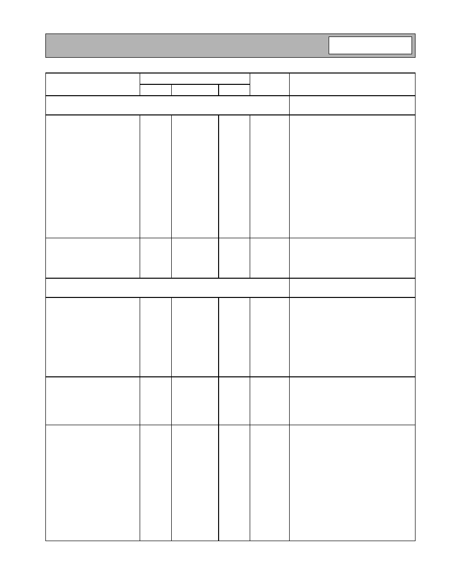
Absolute Maximum Ratings
Parameter
Rating
Unit
Supply Voltage
-0.5 to +5.0
V
DC
Input LO and RF Levels
+6
dBm
Operating Ambient Temperature
-40 to +85
∞C
Storage Temperature
-40 to +150
∞C
Parameter
Specification
Unit
Condition
Min.
Typ.
Max.
Overall
T = 25∞C, V
CC
=2.75V
RF Frequency Range
800 to 900
MHz
1500 to 2200
MHz
1575.42
MHz
GPS band
IF Frequency Range
0.1
400
MHz
Power Supply
Supply Voltage
2.65
2.75
3.15
V
Logic High
1.8
V
Logic Low
0.4
V
Power Down Current
10
µ
A
ENABLE=0
Cellular Band
JCDMA Band
Freq=869MHz to 894MHz
Freq=832MHz to 870MHz
LNA (On)
LNA 50
match
Gain
13.5
15.0
16.5
dB
IPSET=1
13.0
14.5
16.0
dB
IPSET=0
Noise Figure
1.1
1.3
dB
IPSET=1
1.0
1.2
dB
IPSET=0
Input IP3
+9.0
+11.0
dBm
IPSET=1
+5.0
+9.0
dBm
IPSET=0
Current
6.5
mA
IPSET=1
4.5
mA
IPSET=0
Isolation
23
dB
LNA (Off)
Gain
-4.0
-2.5
-1.8
dB
Noise Figure
2.5
4.0
dB
Input IP3
+20.0
+25.0
dBm
Current
0
mA
Isolation
2.5
dB
Mixer - CDMA/JCDMA
LO IN=-4dBm
See note 1 and 2.
Gain
11.5
13.0
14.5
dB
Mixer Preamp ON
1.5
3.0
4.5
dB
Mixer Preamp OFF
Noise Figure
7.5
8.5
dB
Mixer Preamp ON
14.0
16.0
dB
Mixer Preamp OFF
Input IP3
+1.0
+3.5
dBm
Mixer Preamp ON
+11.0
+13.0
dBm
Mixer Preamp OFF
Current
18.5
mA
Mixer Preamp ON/Mixer/LO Input Amps
13.5
mA
Mixer Preamp OFF/Mixer/LO Input Amps
LO to RF Isolation
36
dB
Mixer Preamp ON
dB
Mixer Preamp OFF
LO Frequency Range
600
2300
MHz
High and Low Side LO Injection.
See note 3 and 4.
IF Frequency Range
0.1
183.6
400
MHz
Typical IF frequencies: 85.38MHz,
109.80MHz, 111.85MHz, 183.6MHz
Caution! ESD sensitive device.
RF Micro Devices believes the furnished information is correct and accurate
at the time of this printing. However, RF Micro Devices reserves the right to
make changes to its products without notice. RF Micro Devices does not
assume responsibility for the use of the described product(s).

8-303
RF2498
Rev A3 030711
Parameter
Specification
Unit
Condition
Min.
Typ.
Max.
Cellular Band
JCDMA Band, cont'd
Mixer - FM
LO IN=-4dBm
See note 1 and 2.
Gain
11.5
13.0
14.5
dB
Mixer Preamp ON
1.5
3.0
4.5
dB
Mixer Preamp OFF
Noise Figure
7.5
8.5
dB
Mixer Preamp ON
14.0
16.0
dB
Mixer Preamp OFF
Input IP3
+1.5
+3.5
dBm
Mixer Preamp ON
+11.0
+14.0
dBm
Mixer Preamp OFF
Current
18.5
mA
Mixer Preamp ON/Mixer/LO Input Amps
13.5
mA
Mixer Preamp OFF/Mixer/LO Input Amps
LO to RF Isolation
36
dB
Mixer Preamp ON
dB
Mixer Preamp OFF
LO Frequency Range
600
2300
MHz
High and Low Side LO Injection
See note 3 and 4.
IF Frequency Range
0.1
183.6
400
MHz
Typical IF frequencies: 85.38MHz,
109.80MHz, 111.85MHz, 183.6MHz
Other
LO-IF Isolation
30
dB
RF-IF Isolation
40
dB
LNA Out to Mixer In Isolation
40
dB
LO-LNA In Isolation, Any State
35
dB
US PCS Band
Freq=1930MHz to 1990MHz
Korean PCS Band
Freq=1840MHz to 1870MHz
LNA (On)
LNA 50
match
Gain
13.5
15.5
17.5
dB
IPSET=1
13.0
15.0
16.5
dB
IPSET=0
Noise Figure
1.5
1.8
dB
IPSET=1
1.4
1.7
dB
IPSET=0
Input IP3
+8.0
+12.0
dBm
IPSET=1
-2.0
+4.0
dBm
IPSET=0
Current
6.5
mA
IPSET=1
4.5
mA
IPSET=0
Isolation
20
dB
LNA (Off)
Gain
-6
-4
dB
Noise Figure
4
6
dB
Input IP3
+20.0
+26.0
dBm
Current
0
mA
Isolation
4
dB
Mixer
LO IN=-4dBm
See note 1.
Gain
12.0
14.0
15.5
dB
Mixer Preamp ON
2.5
4.5
6.5
dB
Mixer Preamp OFF
Noise Figure
7.0
8.5
dB
Mixer Preamp ON
15
17
dB
Mixer Preamp OFF
Input IP3
+1.5
+5.0
dBm
Mixer Preamp ON
+11.0
+13.0
dBm
Mixer Preamp OFF
Current
19.0
mA
Mixer Preamp ON/Mixer/LO Input Amps
14.0
mA
Mixer Preamp OFF/Mixer/LO Input Amps
LO to RF Isolation
36
dB
Mixer Preamp ON
30
dB
Mixer Preamp OFF
LO Frequency Range
1600
2400
MHz
High and Low Side LO Injection
IF Frequency Range
0.1
183.6
400
MHz
Typical IF frequencies: 183.6MHz,
210.38MHz, 220.38MHz

8-304
RF2498
Rev A3 030711
Parameter
Specification
Unit
Condition
Min.
Typ.
Max.
Other
LO-IF Isolation
36
dB
RF-IF Isolation
40
dB
LNA Out to Mixer In Isolation
30
40
dB
LO-LNA In Isolation, Any State
35
dB
GPS Band
Freq=1575.42MHz
LNA (On)
LNA 50
match
Gain
17.0
19.0
dB
IPSET=1
16
18
dB
IPSET=0
Noise Figure
1.3
1.7
dB
IPSET=1
1.25
1.7
dB
IPSET=0
Input IP3
+1.0
+5.0
dBm
IPSET=1
-5.0
-1.0
dBm
IPSET=0
Current
6.5
mA
IPSET=1
4.5
mA
IPSET=0
Isolation
20
dB
Mixer
LO IN=-4dBm
See note 1.
Gain
16
18
dB
Noise Figure
5.5
dB
High Side LO Injection.
7.0
dB
Low Side LO Injection.
Input IP3
-7.5
-5.5
dBm
Current
15.5
mA
Preamp/Mixer/LO Input Amps
LO to RF Isolation
dB
LO Frequency Range
1350
1800
MHz
High and Low Side LO Injection
LO Input Power Range
-10
-4
0
dBm
IF Frequency Range
0.1
183.6
400
MHz
Typical IF frequencies: 183.6MHz,
210.38MHz, 220.38MHz
Other
LO-IF Isolation
36
dB
RF-IF Isolation
40
dB
LNA Out to Mixer In Isolation
30
40
dB
LO-LNA In Isolation, Any State
35
dB
Control Lines
Input Capacitance
1
pF
BAND SEL, IF SEL, IP SET, LNA GAIN,
ENABLE, MIX GAIN, TX BUFF ENABLE,
/2 SELECT
Local Oscillator Input
Cellular - CDMA/FM/JCDMA
Input Power
-10
-4
0
dBm
Input Frequency
600
1078
MHz
See note 3. High and Low side injection.
1200
2156
MHz
See note 4. High and Low side injection.
PCS
Input Power
-10
-4
0
dBm
Input Frequency
1600
2300
MHz
High and Low Side LO Injection.
GPS
Input Power
-10
-4
0
dBm
Input Frequency
1350
1800
MHz
High and Low Side LO Injection.

8-305
RF2498
Rev A3 030711
Parameter
Specification
Unit
Condition
Min.
Typ.
Max.
TX (Local Oscillator)
Buffer
Cellular - CDMA/FM/JCDMA
Output Power
-11
-8
dBm
Single-ended 50
load
Output Frequency
600
1078
MHz
See note 3. High and Low Side LO Injection.
Output Power
-11
-6.5
Single-ended 50
load
Output Frequency
1200
2156
MHz
See note 4. High and Low Side LO Injection.
Current Consumption
2
mA
PCS
Output Power
-11
-8
dBm
Single-ended 50
load
Output Frequency
1600
2300
MHz
High and Low Side LO Injection
Current Consumption
2
mA
NOTE 1. Mixer performance can be changed with external IF load/tuning.
NOTE 2. Specifications apply for conditions of LO Divider enabled or disabled.
NOTE 3. LO Divider disabled. LO Divider disabled logic conditions:
A) BAND SELECT=1; /2 SELECT=Immaterial.B) BAND SELECT=0; /2 SELECT=1
NOTE 4. LO Divider enabled. LO Divider enabled logic conditions:
A) BAND SELECT=0; /2 SELECT=0

8-306
RF2498
Rev A3 030711
Evaluation Board Current Measurement
NOTES:
All IDC current numbers include bias circuitry current of 1.5mA to 2.0mA (dependent on mode).
TX Buffer On: Add 2mA to total current.
/2 Select On: Add 2mA to total current.
"X" denotes setting does not impact current.
*For Paging mode set IPSET=0. Total current reduced 2mA.
BAND
SEL
IF
SEL
ENABLE
LNA
GAIN
MIX
GAIN
IP
SET
TX BUFF
ENABLE
/2
SELECT
IDC
(mA)
CDMA Cellular-
High IIP3 LNA Mode*
LNA On, Mixer Preamp On,
TX Buffer Off, /2 Off
0
1
1
1
1
1
0
1
27.0
LNA On, Mixer Preamp Off,
TX Buffer Off, /2 Off
0
1
1
1
0
1
0
1
22.0
LNA Bypassed, Mixer Preamp On,
TX Buffer Off, /2 Off
0
1
1
0
1
X
0
1
20.5
LNA Bypassed, Mixer Preamp Off,
TX Buffer Off, /2 Off
0
1
1
0
0
X
0
1
15.5
FM/JCDMA-
Low Current LNA Mode
LNA On, Mixer Preamp On,
TX Buffer Off, /2 Off
0
0
1
1
1
0
0
1
25.0
LNA On, Mixer Preamp Off,
TX Buffer Off, /2 Off
0
0
1
1
0
0
0
1
20.0
LNA Bypassed, Mixer Preamp On,
TX Buffer Off, /2 Off
0
0
1
0
1
X
0
1
20.5
LNA Bypassed, Mixer Preamp Off,
TX Buffer Off, /2 Off
0
0
1
0
0
X
0
1
15.5
CDMA PCS -
High IIP3 LNA Mode*
LNA On, Mixer Preamp On
TX Buffer Off, /2 Off*
1
1
1
1
1
1
0
1
27.5
LNA On, Mixer Preamp Off
TX Buffer Off, /2 Off*
1
1
1
1
0
1
0
1
25.5
LNA Bypassed, Mixer Preamp On
TX Buffer Off, /2 Off
1
1
1
0
1
X
0
1
21.0
LNA Bypassed, Mixer Preamp Off
TX Buffer Off, /2 Off
1
1
1
0
0
X
0
1
16.0
GPS
LNA On, Mixer On
1
0
1
X
X
0
0
X
24.0

8-307
RF2498
Rev A3 030711
Cascaded Performance (Typical Values for V
CC
=2.75V)
NOTE: All total current numbers include bias circuitry current of 1.5mA to 2.0mA (dependent on mode).
CELL CDMA
LNA ON
LNA OFF
LNA ON
LNA OFF
Parameter
LNA at Max IIP3, IPSET=1
Mixer Preamp On
Mixer Preamp Off
Cascaded:
Gain (dB)
25.0
7.5
15.0
-2.5
Noise Figure (dB)
2.1
13.0
4.5
19.5
Input IP3 (dBm)
-8.5
+8.9
+0.6
+17.6
LO to IF Isolation (dB)
30
30
30
30
IF1 to RF Isolation (dB)
40
40
40
40
IF2 to RF Isolation (dB)
40
40
40
40
LO to LNA IN Isolation (dB)
45
45
45
45
Total Current (mA)
*27.0
20.5
*22.0
15.5
NOTE: Assumes 3dB image filter insertion loss. The TX Buffer Enable is off. Div/2 function is off.
Numbers represent high linearity LNA bias setting IPSET=1.
*For Paging mode set IPSET=0. Total current reduced 2mA.
FM/JCDMA
Parameter
LNA ON
LNA OFF
LNA ON
LNA OFF
Mixer Preamp On
Mixer Preamp Off
Cascaded:
Gain (dB)
24.5
7.5
14.5
-2.5
Noise Figure (dB)
2.1
13.0
4.8
19.5
Input IP3 (dBm)
-8.1
+8.9
+1.6
+18.4
LO to IF Isolation (dB)
30
30
30
30
IF1 to RF Isolation (dB)
40
40
40
40
IF2 to RF Isolation (dB)
40
40
40
40
LO to LNA IN Isolation (dB)
45
45
45
45
Total Current (mA)
25.0
20.5
20.0
15.5
NOTE: Assumes 3dB image filter insertion loss. The TX Buffer Enable is off. Div/2 function is off.
Numbers represent low current LNA bias setting IPSET=0.
PCS CDMA
LNA ON
LNA OFF
LNA ON
LNA OFF
Parameter
LNA at Max IIP3, IPSET=1
Mixer Preamp ON
Mixer Preamp OFF
Cascaded:
Gain (dB)
26.5
7
17.0
-2.5
Noise Figure (dB)
2.2
14
5.0
22
Input IP3 (dBm)
-7.5
+11.8
+0.2
+19.0
LO to IF Isolation (dB)
40
40
40
40
IF1 to RF Isolation (dB)
40
40
40
40
IF2 to RF Isolation (dB)
40
40
40
40
LO to LNA IN Isolation (dB)
40
40
40
40
Total Current (mA)
*27.5
21.0
*22.5
16.0
NOTE: Assumes 3dB image filter insertion loss. The TX Buffer Enable is off. Div/2 function is off.
Numbers represent high linearity LNA bias setting IPSET=1.
*For Paging mode set IPSET=0. Total current reduced 2mA.

8-308
RF2498
Rev A3 030711
Cascaded Performance (Typical Values for V
CC
=2.75V)
NOTE: All total current numbers include bias circuitry current of 1.5mA to 2.0mA (dependent on mode).
Cellular CDMA Gain Control
Parameter
GPS
Cascaded:
High IIP3 LNA Mode, IPSET=1
IPSET=0
Gain (dB)
35.5
34.5
Noise Figure (dB)
1.6
1.6
Input IP3 (dBm)
-23.0
-22.0
Total Current (mA)
24
22
NOTE: Assumes 1.5dB image filter insertion loss. The TX
Buffer Enable is off. /2 Select is off.
Mode
LNA GAIN MIX GAIN
Comments
High Gain
1
1
IMD Test 1 and 2
Mid Gain
1
0
IMD Test 3 and 4
Low Gain
0
1
IMD Test 5 and 6 option 1
Ultra Low Gain
0
0
IMD test 5 and 6 option 2
Note: Contact RFMD for Application note on gain control PCBA layout and software recommendations.

8-309
RF2498
Rev A3 030711
Pin
Function
Type Description
Interface Schematic
1
GPS+
AO
GPS IF output. Open collector.
2
GPS-
AO
GPS IF output. Open collector.
See pin 1.
3
CDMA+
AO
CDMA IF output. Open collector.
4
CDMA-
AO
CDMA IF output. Open collector.
See pin 3.
5
FM+
AO
FM IF output. Open collector. "Current combiner" IF interface
to SAW filter recommended. (See "IF Output Matching Net-
work" section.)
6
FM-
AO
FM IF output. Open collector. "Current combiner" IF interface
to SAW filter recommended. (See "IF Output Matching Net-
work" section.)
See pin 5.
7
VCC2
P
VCC connection for internal LO amplifiers. Internal RF bypass
capacitor. External bypass capacitor between 1nF and 47nF
required.
8
LO IN
AI
LO single-end input. Matched to 50
.
9
LO OUT
AO
LO output. Internal DC block.
10
/2 SELECT
DI
Logic input. Low enables /2 circuitry in cellular mode.
The divider is disabled when BAND SEL (pin 27) is high,
regardless of the state of pin 10. The divider can only be
enabled when BAND SEL is low and pin10 is low. Pin 10 can
be tied to a low state allowing BANDSEL (pin 27) to control the
LO divider function, if using a single LO input source.
See pin 11.
11
TX BUFF
ENABLE
DI
Logic input. High enables TX LO output buffer amplifiers.
12
PCS RFA
VCC
P
VCC connection for PCS mixer preamplifier.
13
PCS MIX IN
AI
PCS mixer RF single-end input.
14
CELL MIX
IN
AI
Cellular mixer RF single-end input. Matched to 50
.
GPS+
GPS-
CDMA+
CDMA-
FM+
FM-
LO IN
70
TX BUF
PCS MIX IN
CELL MIX IN

8-310
RF2498
Rev A3 030711
Pin
Function
Type Description
Interface Schematic
15
MIX GAIN
DI
Logic input. Logic high turns on PCS or cellular mixer preamp
and provides maximum gain. Logic low will bypass the PCS
and cellular mixer preamp.
16
ENABLE
DI
Logic input. Low level powers down the IC.
17
LNA GAIN
DI
Logic input. High activates cellular or PCS LNAs. Low selects
LNA bypass mode for both bands.
18
CELL LNA
OUT
AO
Cellular LNA output. Simple external L-C components
required for matching and VCC supply.
See pin 20.
19
CELL LNA
EMITTER
AO
Cellular LNA emitter. A small inductor connects this pin to
ground. Cellular LNA gain can be adjusted by the inductance.
See pin 20.
20
CELL LNA
IN
AI
Cellular LNA input.
21
PCS LNA
OUT
AO
PCS LNA output. Simple external L-C components required
for matching and VCC supply.
22
IP SET
DI
Logic input. High selects high IIP3 LNA "boost" modes for
GPS, cellular and PCS CDMA paths. Low selects "normal"
LNA IIP3 mode for GPS, cellular and PCS CDMA paths. Bias
setting resistor at pin 31 allows for the adjustment of LNA IIP3
in boost mode.
23
PCS LNA IN
AI
PCS LNA input. For best performance, simple external match-
ing required.
See pin 21.
24
GPS LNA IN
AI
GPS LNA input. For best performance, simple external match-
ing required.
25
GPS LNA
OUT
AO
GPS LNA output. Simple external L-C components required
for matching and VCC supply.
See pin 24.
26
IF SEL
DI
Logic input. High selects CDMA IF outputs; low selects FM or
GPS IF outputs.
27
BAND SEL
DI
Logic input. High level selects PCS or GPS band; low level
selects cellular band. The LO divider circuitry is disabled when
BAND SEL is high, regardless of the state of pin 10 (/2
SELECT). When BAND SEL is low, pin 10 can be selected
high or low. If using a single LO input, pin 10 can be tied to a
low state allowing BAND SEL to control the LO divider func-
tion.
MIX GAIN
ENABLE
LNA GAIN
CELL LNA IN
V
CC
CELL LNA OUT
CELL LNA EMITTER
PCS LNA IN
V
CC
PCS LNA OUT
IP SET
GPS LNA IN
V
CC
GPS LNA OUT
IF SEL
BAND SEL

8-311
RF2498
Rev A3 030711
ISET Pins
ISET1 sets the internal reference voltage for the bias control circuits to all functional blocks. An external resistor of 5.1k
to ground is required. We do not recommend adjusting this resistor value. This resistor is pulled out to allow for a higher
precision off chip value and not as a significant tuning adjustment.
ISET2 sets the DC current through the LNAs in all bands when IPSET is high. Higher resistance to ground results in
lower current through the LNA. Increasing the LNA current will improve the IIP3 of the LNA and slightly increase gain in
all modes. NF typically will get worse as you increase current. Increasing the LNA current in one mode, i.e. Cellular, will
also increase the LNA current for the high IPSET state for PCS and the GPS LNAs as well.
ISET3 sets the DC current through the mixer and mixer preamplifier for all bands. Higher resistance to ground results in
lower current. Lower current will improve mixer NF but will degrade IIP3. Mixer and the mixer preamp gain is not signifi-
cantly changed with current.
Pin
Function
Type Description
Interface Schematic
28
GPS MIX IN
AI
GPS mixer RF single-end input.
29
VCC1
P
DC supply for internal reference, logic control, cellular mixer
preamp, and GPS mixer preamp (PCS mixer preamp has its'
own DC supply, PCS_RFA_VCC). External bypass capacitor
between 1nF and 47nF required.
30
ISET1
AO
Resistor for internal voltage reference setting. Recommended
value 5.1k
.
31
ISET2
AO
Resistor to ground sets the LNA current in boost mode (all
three LNAs). Higher resistance results in lower current.
32
ISET3
AO
Resistor to ground sets preamp and mixer currents in all
bands. Higher resistance results in lower currents.
Pkg
Base
GND
P
Ground connection. The backside of the package should be
soldered to a top side ground pad which is connected to the
ground plane with multiple vias.
Legend:
DI=Digital Input from Baseband Chip
AI=Analog Input
AO=Analog Output
P=V
CC
or GND
GPS MIX IN

8-312
RF2498
Rev A3 030711
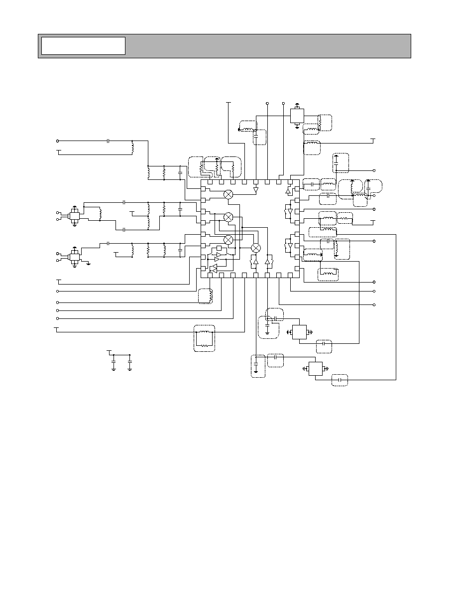
Application Schematic
NOTE: IF output matching component values are dependent on board layout, IF SAW filter and the IF frequency
selected. Please contact RFMD application engineering for assistance with IF output matching.
TBD
7.5 k
TBD
TBD
TBD
TBD
TBD
TBD
TBD
TBD
MIX GAIN
ENABLE
2.4 pF
33 nF
LNA GAIN
33 nF
18 nH
6.8 nH
33 nF
20 k
5.1 k
TBD
32
1
9
17
2
3
4
5
6
7
8
10
11
12
13
14
15
16
24
23
22
21
20
19
18
31
30
29
28
27
26
25
/2
TBD
TBD
4
5
10
9
CDMA
IF SAW
TBD
TBD
TBD
TBD
TBD
4
5
10
9
FM
IF SAW
2.2 nH
DIV EN
TX BUF EN
3.3 nH
1.0 pF
33 nF
IP SET
1.2 nH
10 nH
Cell
RF Saw
6
3
4
1
5
2
OU
T
IN
GND
GND
GND
GND
33 nF
1 pF
PCS
RF Saw
OU
T
IN
GND
GND
GND
GND
6
3
4
1
5
2
33 nF
33 nH
4.7 nH
2.7 nH
10
IF SEL
BAND SEL
V
CC
V
CC
V
CC
V
CC
V
CC
V
CC
V
CC
GPS IF
V
CC
LO IN
LO OUT
V
CC
CELL LNA IN
PCS LNA IN
GPS LNA IN
FM+
FM-
200
CDMA+
CDMA-
NOTES:
1. This resistor sets mixer preamp and mixer currents in all bands.
Lowering the resistance results in higher currents.
2. This resistor sets LNA currents of all bands in boost mode.
Increasing the resistor value results in lower currents.
3. Sets internal bias voltage. Recommend 5.1 k
.
4. DC blocking capacitor.
5. PCS LNA Input Matching. Optimize for NF.
6. Determines trade off between IIP3 and Gain.
Higher value inductor means lower gain and higher IIP3.
7. Cell/PCS LNA Input Matching for optimum IIP3.
Low impedance path to ground at low frequency for optimum IIP3.
8. For cell and PCS mixer input matching.
Note: If any functional blocks are not being used, the unused pins can be left with no connection.
Layout Note:
To minimize losses and radiation, the RF signal traces should be as short as possible. The IF+ and
IF- outputs traces should be symmetrical. All bypass capacitors and matching capacitors must
have a ground via very close to the capacitor. Each capacitor should have its own ground via. All
traces should be 50
transmission lines. Position inductors to reduce coupling (see note 15).
9. PCS Interstage matching. As the value of the inductance is increased,
the PCS mixer preamp gain will decrease and the IIP3 will increase
and vice versa.
10. For optimum NF and input matching. As the value of the capacitance
is increased, the NF will become worse.
11. To optimize performance over temperature and bias.
12. For output matching and a DC supply bias choke.
13. GPS mixer input matching for optimum IIP3.
Low impedance path to ground at low frequency for optimum IIP3.
14. Input or Output matching.
15. Coupling of coils on the input, output, and emitter (where applicable)
of any LNA should be minimized to reduce the risk of oscillation. We
recommend separating the inductors and/or positioning them 90
o
relative to each other.
33 nH
1.2 pF
2.7 nH
33 nF
33 nH
1.2 nH
0.75 pF
15
TBD
V
CC
TBD
GPS
RF Saw
4
1
6
3
5
2
OUT
IN
GN
D
GN
D
GN
D
GN
D
See Notes
12 and 15
See Notes
6 and 15
See
Notes
7 and 15
See Note 4
See Notes
14 and 15
See Notes
12 and 15
See Note 11
See Note 14
See
Note 11
See
Note 2
See Note 3
See Note 1
See Note 9
See Note 8
See Note 4
See Note 4
See Note 14
See Note 8
See Note 4
See
Note 14
See
Note 10
See Note 4
See Notes
14 and 15
See Note 4
See Notes
14 and 15
See
Note 10
See Notes
7 and 15
See Notes
12 and 15
See Note 13
See
Note 4

8-313
RF2498
Rev A3 030711
Evaluation Board Schematic
(Download Bill of Materials from www.rfmd.com.)
C27
6.8 pF
R5
7.5 k
C34
DNI
R1
5.6 k
L10
120 nH
L4
180 nH
VCC
C21
100 pF
C4
6.8 pF
50
µ
strip
J1
GPS IF
C28
6.8 pF
C35
DNI
R2
10 k
L11
120 nH
L6
180 nH
L7
DNI
VCC
C22
100 pF
C17
DNI
C6
5.1 pF
C31
DNI
C11
DNI
L2
DNI
C12
DNI
C2
33 nF
50
µ
strip
J2
CDMA IF
C38
6.8 pF
C36
DNI
R3
24 k
L12
120 nH
L9
DNI
L8
150 nH
C14
DNI
L3
DNI
C15
DNI
C13
DNI
C3
33 nF
50
µ
strip
J3
FM IF
C29
6.8 pF
C5
6.2 pF
VCC
C23
100 pF
C18
DNI
C44
33 nF
VCC
R7
DNI
50
µ
strip
J4
LO IN
L17
2.2 nH
50
µ
strip
J5
LO OUT
DIV EN
TX BUF EN
L18
3.3 nH
C33
33 nF
VCC
C8
33 nF
MIX
GAIN
ENABLE
C16
1 pF
C61
33 nF
C59
DNI
50
µ
strip
J6
PCS MIX IN
50
µ
strip
J7
CELL MIX IN
LNA GAIN
L21
10 nH
C25
100 pF
VCC
C69
2.4 pF
50
µ
strip
J8
CELL LNA OUT
L24
1.2 nH
L16
33 nH
C64
33 nF
50
µ
strip
J9
CELL LNA IN
L22
4.7 nH
L27
2.7 nH
R9
10
C63
33 nF
50
µ
strip
J10
PCS LNA OUT
C26
100 pF
VCC
IP SET
C66
DNI
50
µ
strip
J11
PCS LNA IN
C70
0.75 pF
C62
33 nF
L23
DNI
C19
1.0 pF
50
µ
strip
J12
GPS LNA IN
IF SEL
L20
18 nH
R8
10
C24
100 pF
VCC
L19
6.8 nH
C50
33 nF
50
µ
strip
J13
GPS LNA OUT
C48
DNI
BAND SEL
C41
DNI
C40
33 nF
50
µ
strip
J14
GPS MIX IN
R4
20 k
R6
5.1 k
C43
33 nF
VCC
L13
33 nH
C42
33 nF
2498310, Rev. 1
P3
1
2
3
CON3
GND
GND
P3-1
VCC
C20
1
µ
F
*IF FREQ = 184 MHz
C39
6.8 pF
C37
6.8 pF
32
1
9
17
2
3
4
5
6
7
8
10
11
12
13
14
15
16
24
23
22
21
20
19
18
31
30
29
28
27
26
25
/2
C10
DNI
L26
DNI
L14
DNI
C30
DNI
4
5
10
9
FL3
IF SAW
FL2
CDMA
IF SAW
4
5
10
9
C1
DNI
R10
0
C9
33 nF
C58
DNI
C56
DNI
FL4
Cell RF Saw
6
3
4
1
5
2
OU
T
IN
GND
GND
GND
GND
PCS
RF SAW
FL5
OUT
IN
GN
D
G
N
D
GN
D
G
N
D
6
3
4
1
5
2
FL6
4
1
6
3
5
2
OUT
IN
GN
D
GN
D
GN
D
GN
D
GPS
RF Saw
L25
33 nH
R11
1.2 nH
C7
33 nF
P1
1
2
3
4
CON4
P1-1
C45
33 nF
DIV EN
P1-2
C51
33 nF
IF SEL
P1-3
C52
33 nF
IP SET
P1-4
C49
33 nF
BAND SEL
P2
1
2
3
4
CON4
P2-4
C55
33 nF
LNA GAIN
P2-3
C53
33 nF
MIX GAIN
P2-2
C46
33 nF
TX BUF EN
P2-1
C54
33 nF
ENABLE
R12
200
L15
1.2 pF
L5
33 nF
C32
2.7 nH

8-314
RF2498
Rev A3 030711
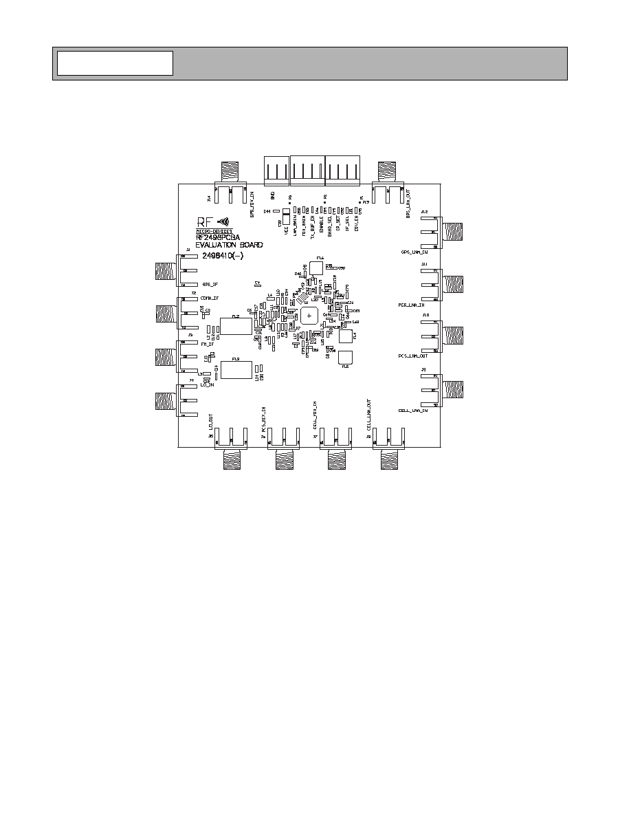
Evaluation Board Layout
Board Size 3.0" x 3.0"
Board Thickness 0.064", Board Material FR-4, Multi-Layer

8-315
RF2498
Rev A3 030711

8-316
RF2498
Rev A3 030711

8-317
RF2498
Rev A3 030711
Cellular Band LO Output Power versus LO Input Power
(Freq=2128MHz, Divider=0(ON), V
CC
2.75V, Temp 25
o
C)
-8.0
-7.5
-7.0
-6.5
-6.0
-10.0
-8.0
-6.0
-4.0
-2.0
0.0
LO Input Power (dBm)
LB-LO Output Power (dBm)
Cellular Band LO Output Power versus LO-Input Power
(Freq=1064MHz, Divider 1(off), V
CC
=2.75V, Temp 25
o
C)
-10.0
-9.5
-9.0
-8.5
-8.0
-7.5
-7.0
-6.5
-6.0
-10.0
-8.0
-6.0
-4.0
-2.0
0.0
LO-Input Power (dBm)
LB-LO Output Power (dBm)
PCS Band LO Output Power versus LO-Input Power
(Freq=2144MHz, V
CC
2.75V, Temp 25
o
C)
-10.0
-9.0
-8.0
-7.0
-6.0
-10.0
-8.0
-6.0
-4.0
-2.0
0.0
LO-Input Power (dBm)
HB-LO Output Power (dBm)
PCS Band LO Output Power versus V
CC
(Freq=2144MHz, Input Power -4dBm, Temp 25
o
C)
-10.00
-9.50
-9.00
-8.50
-8.00
-7.50
-7.00
-6.50
-6.00
2.70
2.75
2.80
2.85
2.90
2.95
3.00
3.05
3.10
3.15
V
CC
(V)
HB-LO Output Power (dBm)
Cellular Band LO Output Power versus V
CC
(Freq=2128MHz, Divider=0 (on), Input Power-4dBm, Temp 25
o
C)
-8.00
-7.50
-7.00
-6.50
-6.00
2.70
2.75
2.80
2.85
2.90
2.95
3.00
3.05
3.10
3.15
V
CC
(V)
LB-LO Output Power (dBm)
Cellular Band LO Output Power versus V
CC
(Freq=1064MHz, Divider=1(off), Input Power-4dBm, Temp 25
o
C)
-10.00
-9.00
-8.00
-7.00
-6.00
2.70
2.75
2.80
2.85
2.90
2.95
3.00
3.05
3.10
3.15
V
CC
(V)
LB-LO Output Power (dBm)

8-318
RF2498
Rev A3 030711
PCB Design Requirements
PCB Surface Finish
The PCB surface finish used for RFMD's qualification process is electroless nickel, immersion gold. Typical thickness is
3
µ
inch to 8
µ
inch gold over 180
µ
inch nickel.
PCB Land Pattern Recommendation
PCB land patterns are based on IPC-SM-782 standards when possible. The pad pattern shown has been developed and
tested for optimized assembly at RFMD; however, it may require some modifications to address company specific
assembly processes. The PCB land pattern has been developed to accommodate lead and package tolerances.
PCB Metal Land Pattern
A
A
A
A
A
A
A
A
B B B B B B B B
C
A
A
A
A
A
A
A
A
B B B B B B B B
3.50 Typ.
0.50 Typ.
0.50 Typ.
0.55 Typ.
0.55 Typ.
1.75 Typ.
1.75 Typ.
3.50 Typ.
A = 0.64 x 0.28 (mm) Typ.
B = 0.28 x 0.64 (mm) Typ.
C = 3.50 (mm) Sq.
Pin 1
Pin 32
Pin 24
Pin 16
Dimensions in mm.
Figure 1. PCB Metal Land Pattern (Top View)

8-319
RF2498
Rev A3 030711
PCB Solder Mask Pattern
Liquid Photo-Imageable (LPI) solder mask is recommended. The solder mask footprint will match what is shown for the
PCB metal land pattern with a 2mil to 3mil expansion to accommodate solder mask registration clearance around all
pads. The center-grounding pad shall also have a solder mask clearance. Expansion of the pads to create solder mask
clearance can be provided in the master data or requested from the PCB fabrication supplier.
A
A
A
A
A
A
A
A
B B B B B B B B
A
A
A
A
A
A
A
A
B
B
B
B
B
B
B
B
C
3.50 Typ.
0.50 Typ.
0.50 Typ.
0.55 Typ.
1.75 Typ.
1.75 Typ.
0.55 Typ.
3.50 Typ.
A = 0.74 x 0.38 (mm) Typ.
B = 0.38 x 0.74 (mm) Typ.
C = 3.60 (mm) Sq.
Pin 1
Pin 32
Pin 24
Pin 16
Dimensions in mm.
Figure 2. PCB Solder Mask Pattern (Top View)

8-320
RF2498
Rev A3 030711


