Se
e Up
gr
aded Pr
od
uc
t RF2514/
RF
25
16
NO
T
FOR
N
EW
DE
SI
GNS
11-11
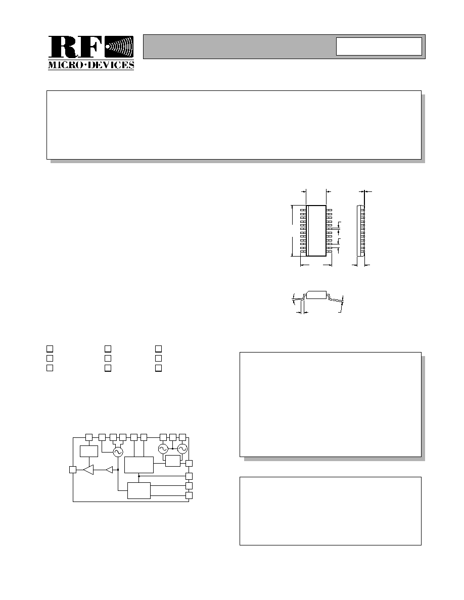
Product Description
Ordering Information
Typical Applications
Features
Functional Block Diagram
RF Micro Devices, Inc.
7628 Thorndike Road
Greensboro, NC 27409, USA
Tel (336) 664 1233
Fax (336) 664 0454
http://www.rfmd.com
Optimum Technology MatchingÆ Applied
Si BJT
GaAs MESFET
GaAs HBT
Si Bi-CMOS
SiGe HBT
Si CMOS
InGaP/HBT
GaN HEMT
SiGe Bi-CMOS
20
18
23
Prescaler
128/129 or
64/65
Phase
Detector &
Charge Pump
24
14
12
15
RESNTR+
L
OOP F
L
T
OSC SEL
RESNTR-
8
TX OUT
1
3
Gain
Control
16
7
13
2
Ref.
Select
OSC B1
OSC E
OSC B2
VREF P
PRESCL OUT
MOD CTRL
DIV CTRL
MO
D
I
N
LVL AD
J
RF2512
UHF TRANSMITTER
∑ Single- or Dual-Channel LO Source
∑ FM/FSK Transmitter
∑ Wireless Data Transmitters
∑ 433/868/915MHz ISM Band Systems
∑ Wireless Security Systems
The RF2512 is a monolithic integrated circuit intended for
use as a low-cost frequency synthesizer and transmitter.
The device is provided in a 24 pin SSOP package and is
designed to provide a phased locked frequency source
for use in local oscillator or transmitter applications. The
chip can be used in FM or FSK applications in the U.S.
915MHz ISM band and European 433MHz or 868MHz
ISM band. The integrated VCO, dual-modulus/dual-divide
(128/129 or 64/65) prescaler, and reference oscillator
require only the addition of an external crystal to provide
a complete phase-locked oscillator. A second reference
oscillator is available to support two channel applications.
∑ Fully Integrated PLL Circuit
∑ 15mW Output Power at 433MHz
∑ 2.7V to 5.0V Supply Voltage
∑ Low Current and Power Down Capability
∑ 300MHz to 1000MHz Frequency Range
∑ Narrowband and Wideband FM
RF2512
UHF Transmitter
RF2512 PCBA-L Fully Assembled Evaluation Board, 433MHz
RF2512 PCBA-M Fully Assembled Evaluation Board, 868MHz
RF2512 PCBA-H Fully Assembled Evaluation Board, 915MHz
0
Rev B13 021008
8∞MAX
0∞MIN
1
0.050
0.016
0.0098
0.0075
0.2440
0.2284
0.025
0.012
0.008
0.0688
0.0532
0.157
0.150
0.0098
0.0040
0.344
0.337
Package Style: SSOP-24
NOT FOR NEW DESIGNS
See Upgraded Product
!
11-12
RF2512
Rev B13 021008
NO
T
FOR
N
EW
DE
SI
GNS
Se
e Up
gr
aded Pr
od
uc
t RF2514/
RF
25
16
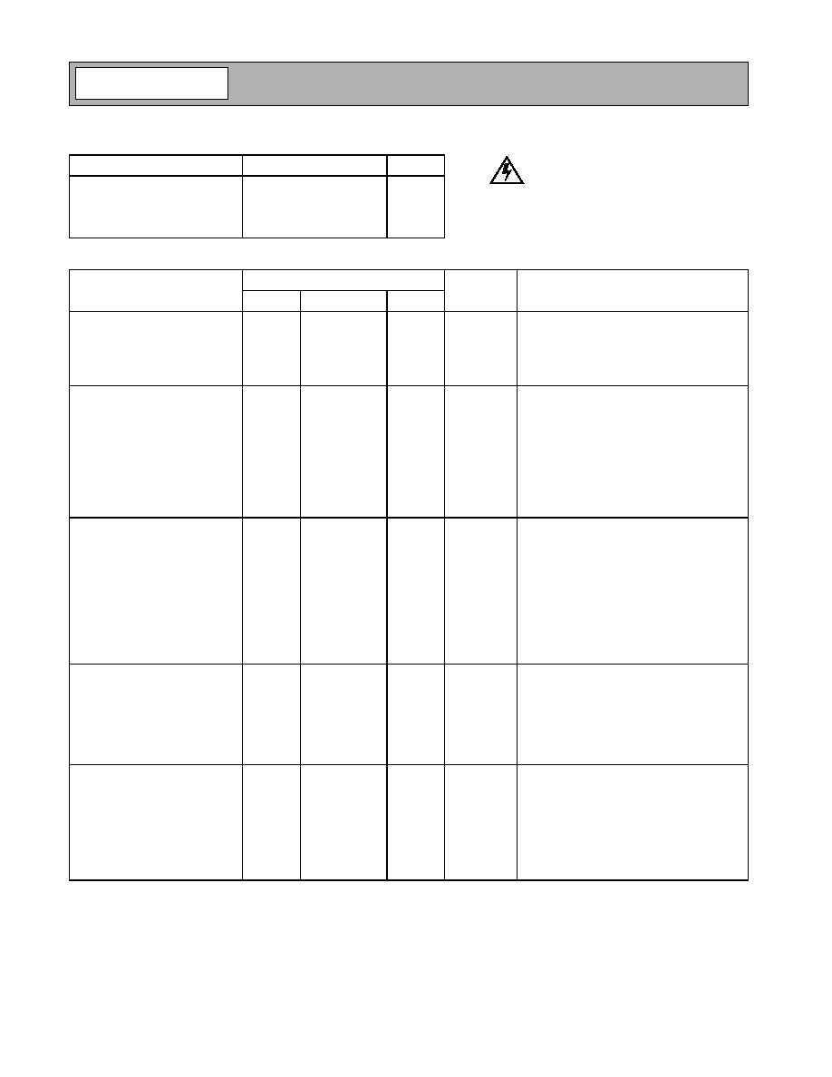
Absolute Maximum Ratings
Parameter
Rating
Unit
Supply Voltage
-0.5 to +5.5
V
DC
Power Down Voltage (V
PD
)
-0.5 to V
CC
V
Operating Ambient Temperature
-40 to +85
∞C
Storage Temperature
-40 to +150
∞C
Parameter
Specification
Unit
Condition
Min.
Typ.
Max.
Overall
T=25 ∞C, V
CC
=3.6V, Freq=915MHz
Frequency Range
300 to 1000
MHz
Modulation
FM/FSK
Modulation Frequency
2
MHz
Maximum FM Deviation
200
kHz
Dependent upon Supply Voltage
PLL and Prescaler
Prescaler Divide Ratio
64/65 or 128/129
PLL Lock TIme
4/PLL BW
ms
The PLL lock time, from power up, is set
externally by the bandwidth of the loop filter.
PLL Phase Noise
-80
dBc/Hz
10kHz Offset, 10kHz loop bandwidth
-100
dBc/Hz
100kHz Offset, 10kHz loop bandwidth
Reference Frequency
17
MHz
Max Crystal R
S
100
Charge Pump Current
-40
+40
µ
A
Transmit Section
Maximum Power Level
+7
+12
dBm
Freq=433MHz
+2
+6
dBm
Freq=915MHz
Power Control Range
15
dB
Power Control Sensitivity
10
dB/V
Antenna Port Impedance
50
TX ENABL="1"
Antenna Port VSWR
1.5:1
TX Mode
Modulation Input Impedance
4
k
Harmonics
-23
dBc
Spurious
dBc
Compliant to Part 15.249 and I-ETS 300 220
Power Down Control
Logic Controls "ON"
2.0
V
Voltage supplied to the input; device is "ON"
Logic Controls "OFF"
1.0
V
Voltage supplied to the input; device is "OFF"
Control Input Impedance
25
k
Turn On Time
5+4/PLL
BW
ms
From Change in OSC SEL,7.075MHz XTAL
Turn Off Time
4
ms
From Change in OSC SEL,7.075MHz XTAL
Power Supply
Voltage
3.6
V
Specifications
2.7 to 5.0
V
Operating limits
Current Consumption
28
31
mA
TX Mode, LVL ADJ=3.6V
10
11
mA
TX Mode, LVL ADJ=0V
8
9
mA
PLL Only
1
µ
A
LVL ADJ=0V, PLL ENABL=0V,
TX ENABL=0V, OSC SEL=0V
Caution! ESD sensitive device.
RF Micro Devices believes the furnished information is correct and accurate
at the time of this printing. However, RF Micro Devices reserves the right to
make changes to its products without notice. RF Micro Devices does not
assume responsibility for the use of the described product(s).
11-13
RF2512
Rev B13 021008
NO
T
FOR
N
EW
DE
SI
GNS
Se
e Up
gr
aded Pr
od
uc
t RF2514/
RF
25
16
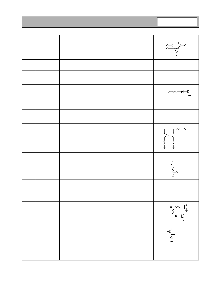
Pin
Function
Description
Interface Schematic
1
OSC B2
This pin is connected directly to the reference oscillator transistor base.
The intended reference oscillator configuration is a modified Colpitts.
An appropriate capacitor as chosen by the customer should be con-
nected between pin 1 and pin 2.
2
OSC E
This pin is connected directly to the emitter of the reference oscillator
transistor. An appropriate capacitor as chosen by the customer should
be connected from this pin to ground.
See pin 1.
3
OSC B1
This pin is connected directly to the reference oscillator transistor base.
The intended reference oscillator configuration is a modified Colpitts.
An appropriate capacitor as chosen by the customer should be con-
nected between pin 3 and pin 2.
See pin 1.
4
PLL ENABL
This pin is used to power up or down the VCO and PLL. A logic high
(PLL ENABL>2.0V) powers up the VCO and PLL electronics. A logic
low (PLL ENABL<1.0V) powers down the PLL and VCO.
5
GND1
Ground connection for the PA buffer amp. Keep traces physically short
and connect immediately to ground plane for best performance.
6
VCC3
This pin is used to supply DC bias to the transmitter PA. A RF bypass
capacitor should be connected directly to this pin and returned to
ground. A 100pF capacitor is recommended for 915MHz applications.
A 220pF capacitor is recommended for 433MHz applications.
7
LVL ADJ
This pin is used to vary the transmitter output power. An output level
adjustment range greater than 12dB is provided through analog volt-
age control of this pin. DC current of the transmitter power amp ia also
reduced with output power. This pin MUST be low when the transmitter
is disabled.
8
TX OUT
RF output pin for the transmitter electronics. TX OUT output impedance
is a low impedance when the transmitter is enabled. TX OUT is a high
impedance when the transmitter is disabled.
9
GND2
Ground connection for the Tx PA functions. Keep traces physically
short and connect immediately to ground plane for best performance.
10
VCC1
This pin is used to supply DC bias to the PA buffer amp. A RF bypass
capacitor should be connected directly to this pin and returned to
ground. A 100pF capacitor is recommended for 915MHz applications.
A 220pF capacitor is recommended for 433MHz applications.
11
TX ENABL
Enables the transmitter circuits. TX ENABL>2.0V powers up all trans-
mitter functions. TX ENABL<1.0V turns off all transmitter functions
except the PLL functions.
12
PRESCL
OUT
Dual-modulus/Dual-divide prescaler output. The output can be inter-
faced to an external PLL IC for additional flexibility in frequency pro-
gramming.
13
VREF P
Bias voltage reference pin for bypassing the prescaler and phase
detector. The bypass capacitor should be of appropriate size to provide
filtering of the reference crystal frequency and be connected directly to
this pin.
OSC E
OSC B1
OSC B2
50 k
PLL ENABL
400
4 k
LVL ADJ
40 k
TX OUT
20
V
CC
40 k
20 k
TX ENABL
PRESCL
OUT

11-14
RF2512
Rev B13 021008
NO
T
FOR
N
EW
DE
SI
GNS
Se
e Up
gr
aded Pr
od
uc
t RF2514/
RF
25
16
Pin
Function
Description
Interface Schematic
14
MOD CTRL
This pin is used to select the prescaler modulus. A logic "high" selects
64 or 128 for the prescaler divisor. A logic "low" selects 65 or 129 for
the prescaler divisor.
15
DIV CTRL
This pin is used to select the desired prescaler divisor. A logic "high"
selects the 64/65 divisor. A logic low selects the 128/129 divisor.
16
MOD IN
FM analog or digital modulation can be imparted to the VCO through
this pin. The VCO varies in accordance to the voltage level presented
to this pin. To set the deviation to a desired level, a voltage divider refer-
enced to Vcc is the recommended. Because the modulation varactors
are part of the resonator tank, the deviation is slightly dependent upon
the components used in the external tank.
See pin 18.
17
VCC2
This pin is used to is supply DC bias to the VCO, prescaler, and PLL.
18
RESNTR-
The RESNTR pins are used to supply DC voltage to the VCO, as well
as to tune the center frequency of the VCO. Equal value inductors
should be connected to this pin and pin 20.
19
NC
Not internally connected.
20
RESNTR+
See pin 18.
See pin 18.
21
GND3
GND is the ground shared on chip by the VCO, prescaler, and PLL
electronics. Keep traces physically short and connect immediately to
ground plane for best performance.
22
NC
Not internally connected.
23
LOOP FLT
Output of the charge pump. An RC network from this pin to ground is
used to establish the PLL bandwidth.
24
OSC SEL
A logic high (OSC SEL>2.0V) applied to this pin powers on reference
oscillator 2 and powers down reference oscillator 1. A logic low (OSC
SEL<1.0V) applied to this pin powers on reference oscillator 1 and
powers down reference oscillator 2.
ESD
This diode structure is used to provide electrostatic discharge protec-
tion to 3kV using the Human body model. The following pins are pro-
tected: 1-3, 9, 10, 12-15, 17, 21, 23.
MOD CTL
DIV CTL
RESNTR-
RESNTR+
4 k
MOD IN
LOOP FLT
V
CC
V
CC

11-15
RF2512
Rev B13 021008
NO
T
FOR
N
EW
DE
SI
GNS
Se
e Up
gr
aded Pr
od
uc
t RF2514/
RF
25
16
RF2512 Theory of Operation
Introduction
The RF2512 is a low cost FM/FSK UHF transmitter
designed for applications operating within the fre-
quency range of 300MHz to 1000MHz. In particular, it
is intended for 315/433/868MHz band systems, remote
keyless entry systems, and FCC Part 15.231 periodic
transmitters. It can also be used as a single- or dual-
channel local oscillator signal source. The integrated
VCO, phase detector, prescaler, and reference oscilla-
tor require only the addition of an external crystal to
provide a complete phase-locked loop.
The RF2512 is provided in a 24-pin SSOP-24 package
and is designed to operate from a supply voltage rang-
ing from 2.7V to 5.0V, accommodating designs using
three NiCd battery cells, two AAA flashlight cells, or a
lithium button battery. The device is capable of provid-
ing up to 15mW output power into a 50
load
(+11.8dBm) and is intended to comply with FCC
requirements for unlicensed remote control transmit-
ters.
RF2512 Functional Blocks
A PLL consists of a reference oscillator, a phase detec-
tor, a loop filter, a voltage controlled oscillator (VCO),
and a programmable divider in the feedback path. The
RF2512 includes all of these internally except for the
loop filter and the reference oscillator's crystal and two
feedback capacitors.
The
reference oscillators are Colpitts type oscillators.
Pin 1 (OSC B2), pin 2 (OSC E), and pin 3 (OSC B1)
provide connections to the internal transistors that are
used as the reference oscillators. The Colpitts configu-
ration is a low parts count topology with reliable perfor-
mance and reasonable phase noise. Alternatively, an
external signal could be injected into the base of either
transistor. The drive level should, in either case, be
around 500mV
PP
. This level prevents overdriving the
device and keeps the phase noise and reference spurs
to a minimum.
The user sets which oscillator is operational by setting
pin 24 (OSC SEL) either high or low. This allows the
implementation of two channel systems.
The
prescaler divides the Voltage Controlled Oscilla-
tor (VCO) frequency down by either 64/65 or 128/129,
using a series of flip-flops, depending upon the logic
level present at pin 15 (DIV CTRL). A high logic level
will select the 64/65 divisor. A low logic level will select
the 128/129 divisor. This divided signal is then fed into
the phase detector where it is compared with the refer-
ence frequency.
In addition to the DIV CTRL setting, one also sets the
prescaler modulus by setting pin 14 (MOD CTRL)
either high or low. A high logic level will select the
64/128 divisor. A low logic level will select the 65/129
divisor.
Pin 12 (PRESCL OUT) provides access to the pres-
caler output. This is used for interfacing to an external
PLL IC.
The RF2512 contains an onboard phase detector and
charge pump. The
phase detector compares the
phase of the reference oscillator to the phase of the
VCO. The phase detector is implemented using flip-
flops in a topology referred to as either "digital
phase/frequency detector" or "digital tri-state compara-
tor". The circuit consists of two D flip-flops whose out-
puts are combined with a NAND gate which is then tied
to the reset on each flip-flop. The outputs of the flip-
flops are also connected to the charge pump. Each flip-
flop output signal is a series of pulses whose fre-
quency is related to the flip-flop input frequency.
When both inputs of the flip-flops are identical, the sig-
nals are both frequency and phase locked. If they are
different, they will provide signals to the charge pump
which will either charge or discharge the loop filter or
enter into a high impedance state. This is where the
name "tri-state comparator" comes from.
The main benefit of this type of detector it's ability to
correct for errors in both phase and frequency. When
locked, the detector uses phase error for correction.
When unlocked, it will use the frequency error for cor-
rection. This type of detector will lock under all condi-
tions.
The prescaler and the phase detector bias voltage is
brought out through pin 13 (VREF P). This allows
bypassing of the of these two circuits to filter the refer-
ence crystal frequency.
The
charge pump consists of two transistors, one for
charging the loop filter and the other for discharging
the loop filter. It's inputs are the outputs of the phase
detector flip-flops. Since there are two flip-flops, there
are four possible states. If both amplifier inputs are low,
then the amplifier pair goes into a high impedance
state, maintaining the charge on the loop filter. The
11-16
RF2512
Rev B13 021008
NO
T
FOR
N
EW
DE
SI
GNS
Se
e Up
gr
aded Pr
od
uc
t RF2514/
RF
25
16
state where both inputs are high will not occur. The
other states are either charging or discharging the loop
filter. The loop filter integrates the pulses coming from
the charge pump to create a control voltage for the
voltage controlled oscillator.
The
voltage controlled oscillator (VCO) is a tuned
differential amplifier with the bases and collectors
cross coupled to provide positive feedback and a 360∞
phase shift. The tuned circuit is located in the collec-
tors. It is comprised an external varactor, a capacitor
and external inductors. The designer selects the induc-
tors for the desired frequency of operation. These
inductors also provide DC bias for the VCO. The output
of the VCO is buffered and applied to the prescaler cir-
cuit, where it is divided down and compared to the ref-
erence oscillator frequency.
The PLL and VCO circuitry can be enabled by setting
applying a "high" logic level to pin 4 (PLL ENABL).
Conversely, the PLL and VCO circuitry will be turned
off if the level is tied "low".
The
transmit amplifier is a two stage amplifier con-
sisting of a driver and an open collector final stage. It is
capable of providing 12dBm of output power into a
50
load while operating from a 3.6V power supply.
The output power is adjustable by the setting of pin 7
(LVL ADJ). This analog input allows the designer a
12dB range of output power. As the LVL ADJ voltage is
reduced, the output power and current consumption
are reduced. LVL ADJ must be low when the transmit-
ter is disabled.
Additionally, the transmitter circuitry can be disabled
entirely by applying a "low" logic level to pin 11 (TX
ENABL). During transmission, this pin should be tied
"high". This pin controls all circuitry except for the PLL
circuitry.
During transmission the transmitter is enabled and the
impedance of the output pin, pin 8 (TX OUT), is low.
When the transmitter is not enabled, the impedance
becomes high.
The RF2512 contains onboard band gap reference
voltage circuitry which provides a stable
DC bias over
varying temperature and supply voltages.
Designing with the RF2512
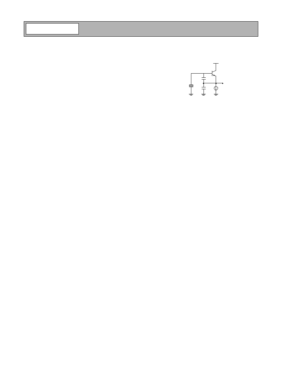
The
reference oscillator is built around the onboard
transistor at pins 1, 2 and 3. The intended topology is
of a Colpitts oscillator. The Colpitts oscillator is quite
common and requires few external components, mak-
ing it ideal for low cost solutions. The topology of this
type of oscillator is as seen in the following figure.
This type of oscillator is a parallel resonant circuit for a
fundamental mode crystal. The transistor amplifier is
an emitter follower and the voltage gain is developed
by the tapped capacitor impedance transformer. The
series combination of C1 and C2 act in parallel with the
input capacitance of the transistor to capacitively load
the crystal.
The nominal capacitor values can be calculated with
the following equations.
and
The load capacitance is usually 32pF. The variable freq
is the oscillator frequency in MHz. The frequency can
be adjusted by either changing C
2
or by placing a vari-
able capacitor in series with the crystal. As an exam-
ple, assume a desired frequency of 14MHz and a load
capacitance of 32pF. C
1
=137.1pF and C
2
=41.7pF.
These capacitor values provide a starting point. The
drive level of the oscillator should be checked by look-
ing at the signal at pin 2 (OSC E). It has been found
that the level at this pin should generally be around
500mV
PP
or less. This will reduce the reference spur
levels and reduce noise from distortion. If this level is
higher than 500mV
PP
then decrease the value of C
1
.
The values of these capacitors are usually tweaked
during design to meet performance goals, such as
minimizing the start-up time.
Additionally, by placing a variable capacitor in series
with the crystal, one is able to adjust the frequency.
This will also alter the drive level, so it should be
checked again.
An important part of the overall design is the
voltage
controlled oscillator. The VCO is configured as a dif-
ferential amplifier. The VCO is tuned via the external
inductors, capacitor, and varactor. The varactor capaci-
V
CC
C2
C1
X1
C
1
60 C
load
freq
MHz
------------------------
=
C
2
1
1
C
load
-------------
1
C
1
------
≠
--------------------------
=

11-17
RF2512
Rev B13 021008
NO
T
FOR
N
EW
DE
SI
GNS
Se
e Up
gr
aded Pr
od
uc
t RF2514/
RF
25
16
tance is set by the loop filter output voltage through a
4k
resistor.
To tune the VCO the designer only needs to calculate
the value of the inductors connected to pins 18 and 20
(RESNTR- and RESNTR+). The inductor value is
determined by the following equation.
In this equation, f is the desired operating frequency
and L is the value of the inductor required. The value C
is the amount of capacitance presented by the varac-
tor, capacitor and parasitics. The factor of one-half is
due to the inductors being in each leg.
The setup of the VCO can be summarized as follows.
First, open the loop. Next, get the VCO to run on the
desired frequency by selecting the proper inductor and
capacitor values. The capacitor value will need to
include the varactor and circuit parasitics. After the
VCO is running at the desired frequency, then set the
VCO sensitivity.
The sensitivity is determined by connecting the control
voltage input point to ground and noting the frequency.
Then connect the same point to the supply and again
note the frequency. The difference between these two
frequencies divided by the supply voltage is the VCO
sensitivity expressed in Hz/V. Increasing the inductor
value while decreasing the capacitor value will
increase the sensitivity. Decreasing the inductor value
while increasing the capacitor value will lower the sen-
sitivity.
When increasing or decreasing component values,
make sure that the center frequency remains constant.
Finally, close the loop.
External to the part, the designer needs to implement a
loop filter to complete the PLL. The loop filter converts
the output of the charge pump into a voltage that is
used to control the VCO. Internally, the VCO is con-
nected to the charge pump output through a 4k
resis-
tor. The loop filter is then connected in parallel to this
point at pin 23 (LOOP FLT). This limits the loop filter
topology to a second order filter usually consisting of a
shunt capacitor and a shunt series RC. A passive filter
is most common, as it is a low cost and low noise
design. An additional pole could be used for reducing
the reference spurs, however there is not a way to add
the series resistor. This should not be a reason for con-
cern however.
The schematic of the loop filter is
The transfer function is
where the time constants are defined as
and
The frequency at which unity gain occurs is given by
This is also the loop bandwidth.
If the phase margin (PM) and the loop bandwidth
(
LBW
) are known, it is possible to calculate the time
constants. These are found using the equations
and
RESNTR-
RESNTR+
LOOP
FLT
4 k
L
L
L
1
2
f
----------------
2
1
C
---- 1
2
---
=
V
CC
R2
C2
C1
VCO
Loop Filter
Charge Pump
F s
( )
R
2
s
2
1
+
s
2
s
1
1
+
(
)
------------------------------------------
=
2
R
2
C
2
=
1
R
2
C
1
C
2
C
1
C
2
+
-------------------
=
LBW
1
1
2
-------------------
=
1
PM
(
)
sec
PM
(
)
tan
≠
LBW
--------------------------------------------------
=
2
1
2
LBW
1
--------------------------
=

11-18
RF2512
Rev B13 021008
NO
T
FOR
N
EW
DE
SI
GNS
Se
e Up
gr
aded Pr
od
uc
t RF2514/
RF
25
16
With these known, it is then possible to determine the
values of the filter components.
As an example, consider a loop bandwidth of 50kHz, a
phase margin of 45∞, a divide ratio of 64, a K
VCO
of
20MHz/V, and a K
PD
of 40
µ
A/2
rad. Time constant
1
is 1.31848
µ
s, time constant
2
is 7.68468
µ
s, C
1
is
8.35pF, C
2
is 40.3pF, and R
2
is 190.6k
.
In order to perform these calculations, one will need to
know the value of two constants, K
VCO
and K
PD
. K
PD
is
calculated by dividing the charge pump current by 2
.
For the RF2512, the charge pump current is 40
µ
A.
K
VCO
is best found empirically as it will change with
frequency and board parasitics. By briefly connecting
pin 23 (LOOP FLT) to VCC and then to ground, the fre-
quency tuning range of the VCO can be seen. Dividing
the difference between these two frequencies by the
difference in the voltage gives K
VCO
in MHz/V.
The control lines provide an
interface for connecting
the device to a microcontroller or other signal generat-
ing mechanism. The designer can treat pin 16 (MOD
IN), pin 15 (DIV CTRL), pin 14 (MOD CTRL) and pin 7
(LVL ADJ) as control pins whose voltage level can be
set.
General
RF bypassing techniques must be observed
to get the best performance. Choose capacitors such
that they are series resonant near the frequency of
operation.
Board layout is always an area in which great care
must be taken. The board material and thickness are
used in calculating the RF line widths. The use of vias
for connection to the ground plane allows one to con-
nect to ground as close as possible to ground pins.
When laying out the traces around the VCO, it is desir-
able to keep the parasitics equal between the two legs.
This will allow equal valued inductors to be used.
Pre-compliance testing should be performed during
the design process. This can be done with a GTEM cell
or at a compliance testing laboratory. It is recom-
mended that pre-compliance testing be performed so
that there are no surprises during final compliance
testing. This will help keep the product development
and release on schedule.
Working with a laboratory offers the benefit of years of
compliance testing experience and familiarity with the
regulatory issues. Also, the laboratory can often pro-
vide feedback that will help the designer make the
product compliant.
On the other hand, having a GTEM cell or an open air
test site locally offers the designer the ability to rapidly
determine whether or not design changes impact the
product's compliance. Set-up of an open air test site
and the associated calibration is not trivial. An alterna-
tive is to use a GTEM test cell.
After the design has been completed and passes com-
pliance testing, application will need to be made with
the respective regulatory bodies for the geographic
region in which the product will be operated to obtain
final certifications.
Conclusions
The RF2512 is an FM/FSK UHF transmitter that fea-
tures a phase-locked output. This device is suitable for
use in a CFR Part 15.231 compliant product as well as
a local oscillator signal source. Further, the RF2512 is
packaged in a low cost SSOP-24 plastic package and
requires few external parts, thus making it suitable for
low cost designs.
C
1
1
2
-----
K
PD
K
VCO
2
LBW
N
-----------------------------
1
LBW
2
(
)
2
+
1
LBW
1
(
)
2
+
----------------------------------------
=
C
2
C
1
2
1
----- 1
≠
=
R
2
2
C
2
------
=
11-19
RF2512
Rev B13 021008
NO
T
FOR
N
EW
DE
SI
GNS
Se
e Up
gr
aded Pr
od
uc
t RF2514/
RF
25
16
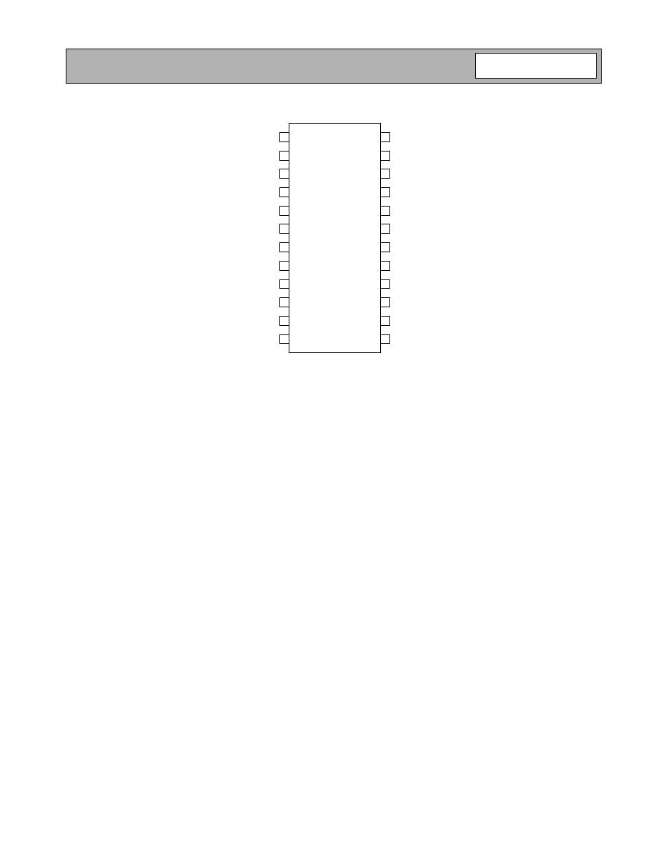
Pin Out
1
2
3
4
5
6
7
8
9
10
11
12
24
23
22
21
20
19
18
17
16
15
14
13
OSC B2
OSC E
OSC B1
PLL ENABL
GND1
VCC3
LVL ADJ
TX OUT
GND2
VCC1
TX ENABL
PRESCL OUT
OSC SEL
LOOP FLT
NC
GND3
RESNTR+
NC
RESNTR-
VCC2
MOD IN
DIV CTRL
MOD CTRL
VREF P

11-20
RF2512
Rev B13 021008
NO
T
FOR
N
EW
DE
SI
GNS
Se
e Up
gr
aded Pr
od
uc
t RF2514/
RF
25
16
Evaluation Board Schematic
H (915MHz) and M (868MHz) Boards
(Download Bill of Materials from www.rfmd.com.)
1
2
3
4
5
6
7
8
9
10
11
12
24
23
22
21
20
19
18
17
16
15
14
13
Phase
Detector/
Charge Pump
Prescaler
Ref
Select
Gain
Control
C3
100 pF
C1
100 pF
C2*
100 pF
X1
X2*
R5*
0
PLL ON
C8
100 pF
C7
4 pF
L1
8.2 nH
C6
4 pF
C18
0.1 uF
50
µ
strip
J1
RF OUT
VCC
LVL ADJ
C4
10 nF
C5
22 pF
VCC
C9
10 nF
C10
22 pF
TX EN
R3*
TBD
PRESC OUT
D1
SMV
1233-011
C15
3 pF
L2
6.8 nH
L3
6.8 nH
L4
56 nH
R2
4.3 k
C12
10 nF
C13
22 pF
C14
4.7
µ
F
C16
47 nF
C17
4.7 nF
R1
OSC SEL
MOD CTL
DIV 64
50
µ
strip
J2
MOD IN
C11
0.1
µ
F
2512401A, 402B
M (868MHz)
H (915MHz)
Board
13.57734
7.15909
X1 (MHz)
13.41015
7.07549
X2 (MHz)
6.8
4.7
L2 (nH)
1.2
2.2
R1 (k
)
6.8
4.7
L3 (nH)
1
2
3
P4
CON3
P4-1
DIV 64
GND
P4-3
MOD CTL
P2-1
PRESC OUT
GND
P2-3
TX EN
1
2
3
P2
CON3
P1
1
2
3
CON3
P1-3
PLL ON
GND
P1-1
LVL ADJ
D2*
D3*
R7*
0
AUDIO
P3-1
AUDIO
GND
P3-3
OSCSLT
GND
P3-5
VCC
1
2
3
4
5
P3
CON5
C20
3-10 pF
R6*
0

11-21
RF2512
Rev B13 021008
NO
T
FOR
N
EW
DE
SI
GNS
Se
e Up
gr
aded Pr
od
uc
t RF2514/
RF
25
16
Evaluation Board Schematic
L (433MHz) Board
1
2
3
4
5
6
7
8
9
10
11
12
24
23
22
21
20
19
18
17
16
15
14
13
Phase
Detector/
Charge Pump
Prescaler
Ref
Select
Gain
Control
C3
100 pF
C1
100 pF
C2*
100 pF
X1
6.78 MHz
X2*
6.612813
MHz
R5*
0
PLL ON
C8
100 pF
C7
8 pF
L2
22 nH
L1
22 nH
C6
15 pF
C18
0.1 uF
50
µ
strip
J1
RF OUT
VCC
LVL ADJ
C4
0.01 uF
C5
22 pF
C19
8 pF
VCC
C9
10 nF
C10
22 pF
TX EN
R3*
TBD
PRESC OUT
D1
SMV
1233-011
C15
5 pF
L3
27 nH
L4
27 nH
L5
220 nH
R2
4.3 k
C12
10 nF
C13
22 pF
C14
4.7
µ
F
C16
47 nF
C17
4.7 nF
R1
2 k
OSC SEL
MOD CTL
DIV 64
50
µ
strip
J2
MOD IN
C11
0.1
µ
F
2512400A
P1
1
2
3
CON3
P1-3
PLL ON
GND
P1-1
LVL ADJ
P2-3
TX EN
GND
P2-1
PRESC OUT
1
2
3
CON3
P2
P4-1
DIV 64
GND
P4-3
MOD CTL
1
2
3
CON3
P4
1
2
3
4
5
P3
CON5
P3-1
AUDIO
P3-3
OSCSLT
GND
P3-5
VCC
GND
R6*
0
C20
3-10 pF
D2*
D3*
R7*
0
AUDIO
*Denotes optional. These parts are not normally populated.
11-22
RF2512
Rev B13 021008
NO
T
FOR
N
EW
DE
SI
GNS
Se
e Up
gr
aded Pr
od
uc
t RF2514/
RF
25
16
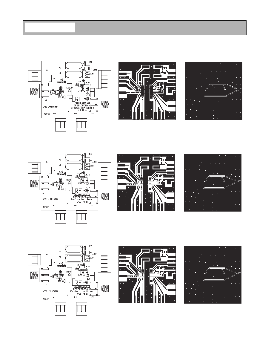
Evaluation Board Layout 433MHz
Board Size 1.5" x 1.5"
Evaluation Board Layout 868MHz
Board Size 1.5" x 1.5"
Evaluation Board Layout 915MHz
Board Size 1.5" x 1.5"
11-23
RF2512
Rev B13 021008
NO
T
FOR
N
EW
DE
SI
GNS
Se
e Up
gr
aded Pr
od
uc
t RF2514/
RF
25
16
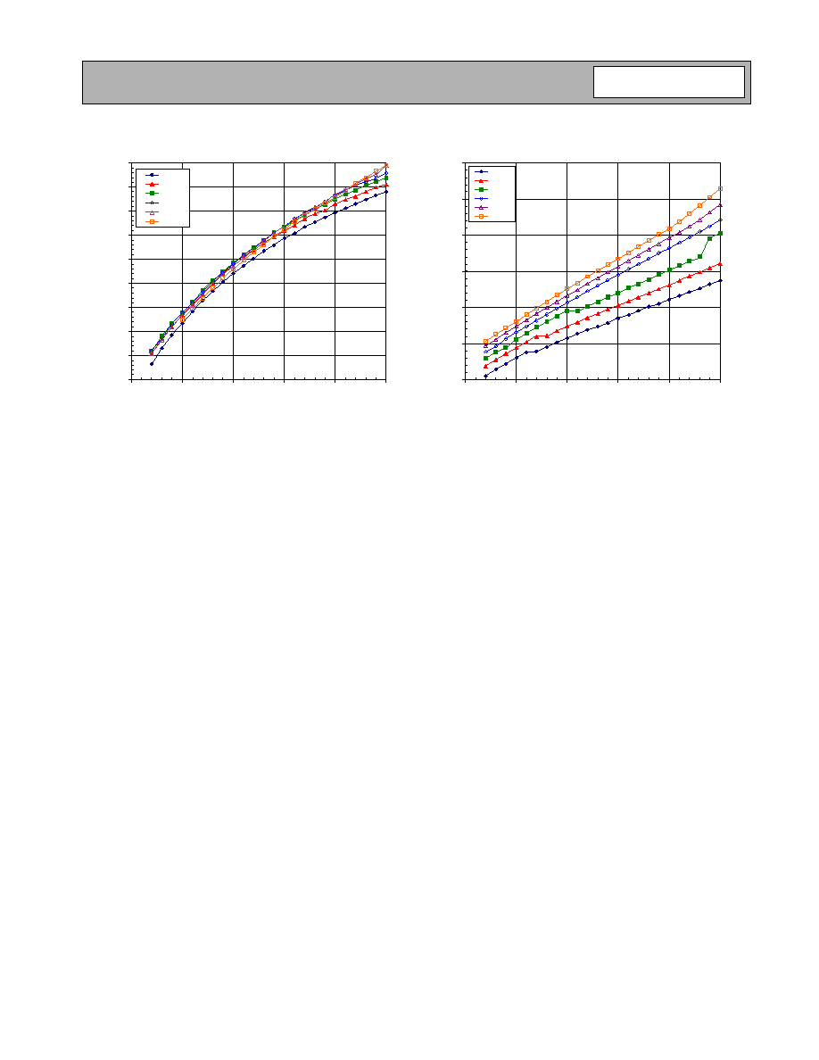
TX Power versus V
CC
Level Adjust = V
CC
, 915 MHZ
2.0
3.0
4.0
5.0
6.0
7.0
8.0
9.0
10.0
11.0
2.5
3.0
3.5
4.0
4.5
5.0
V
CC
(V)
TX Power (dBm)
-40∞C
-15∞C
+10∞C
+35∞C
+60∞C
+85∞C
I
CC
versus V
CC
Level Adjust = V
CC
, 915 MHz
15.0
20.0
25.0
30.0
35.0
40.0
45.0
2.5
3.0
3.5
4.0
4.5
5.0
V
CC
(V)
I
CC
(mA)
-40∞C
-15∞C
+10∞C
+35∞C
+60∞C
+85∞C

11-24
RF2512
Rev B13 021008
NO
T
FOR
N
EW
DE
SI
GNS
Se
e Up
gr
aded Pr
od
uc
t RF2514/
RF
25
16